EP3148303A1 - Elektrische schaltungsanordnung mit kondensator mit gehäusefunktion - Google Patents
Elektrische schaltungsanordnung mit kondensator mit gehäusefunktion Download PDFInfo
- Publication number
- EP3148303A1 EP3148303A1 EP15186521.9A EP15186521A EP3148303A1 EP 3148303 A1 EP3148303 A1 EP 3148303A1 EP 15186521 A EP15186521 A EP 15186521A EP 3148303 A1 EP3148303 A1 EP 3148303A1
- Authority
- EP
- European Patent Office
- Prior art keywords
- capacitor
- arrangement
- circuit
- circuit arrangement
- arrangement according
- Prior art date
- Legal status (The legal status is an assumption and is not a legal conclusion. Google has not performed a legal analysis and makes no representation as to the accuracy of the status listed.)
- Withdrawn
Links
- 239000003990 capacitor Substances 0.000 title claims abstract description 212
- 238000001816 cooling Methods 0.000 claims description 8
- 239000004065 semiconductor Substances 0.000 description 9
- 238000004519 manufacturing process Methods 0.000 description 4
- 230000000712 assembly Effects 0.000 description 2
- 238000000429 assembly Methods 0.000 description 2
- 238000009434 installation Methods 0.000 description 2
- 238000004804 winding Methods 0.000 description 2
- 230000007547 defect Effects 0.000 description 1
- 230000001419 dependent effect Effects 0.000 description 1
- 238000010586 diagram Methods 0.000 description 1
- 238000005516 engineering process Methods 0.000 description 1
- 239000011796 hollow space material Substances 0.000 description 1
- 230000002093 peripheral effect Effects 0.000 description 1
- 230000001172 regenerating effect Effects 0.000 description 1
- 230000035939 shock Effects 0.000 description 1
- 238000005476 soldering Methods 0.000 description 1
Images

Classifications
-
- H—ELECTRICITY
- H01—ELECTRIC ELEMENTS
- H01G—CAPACITORS; CAPACITORS, RECTIFIERS, DETECTORS, SWITCHING DEVICES, LIGHT-SENSITIVE OR TEMPERATURE-SENSITIVE DEVICES OF THE ELECTROLYTIC TYPE
- H01G4/00—Fixed capacitors; Processes of their manufacture
- H01G4/40—Structural combinations of fixed capacitors with other electric elements, the structure mainly consisting of a capacitor, e.g. RC combinations
-
- H—ELECTRICITY
- H01—ELECTRIC ELEMENTS
- H01G—CAPACITORS; CAPACITORS, RECTIFIERS, DETECTORS, SWITCHING DEVICES, LIGHT-SENSITIVE OR TEMPERATURE-SENSITIVE DEVICES OF THE ELECTROLYTIC TYPE
- H01G2/00—Details of capacitors not covered by a single one of groups H01G4/00-H01G11/00
- H01G2/08—Cooling arrangements; Heating arrangements; Ventilating arrangements
-
- H—ELECTRICITY
- H01—ELECTRIC ELEMENTS
- H01G—CAPACITORS; CAPACITORS, RECTIFIERS, DETECTORS, SWITCHING DEVICES, LIGHT-SENSITIVE OR TEMPERATURE-SENSITIVE DEVICES OF THE ELECTROLYTIC TYPE
- H01G2/00—Details of capacitors not covered by a single one of groups H01G4/00-H01G11/00
- H01G2/10—Housing; Encapsulation
-
- H—ELECTRICITY
- H01—ELECTRIC ELEMENTS
- H01G—CAPACITORS; CAPACITORS, RECTIFIERS, DETECTORS, SWITCHING DEVICES, LIGHT-SENSITIVE OR TEMPERATURE-SENSITIVE DEVICES OF THE ELECTROLYTIC TYPE
- H01G4/00—Fixed capacitors; Processes of their manufacture
- H01G4/28—Tubular capacitors
-
- H—ELECTRICITY
- H01—ELECTRIC ELEMENTS
- H01G—CAPACITORS; CAPACITORS, RECTIFIERS, DETECTORS, SWITCHING DEVICES, LIGHT-SENSITIVE OR TEMPERATURE-SENSITIVE DEVICES OF THE ELECTROLYTIC TYPE
- H01G4/00—Fixed capacitors; Processes of their manufacture
- H01G4/32—Wound capacitors
-
- H—ELECTRICITY
- H01—ELECTRIC ELEMENTS
- H01G—CAPACITORS; CAPACITORS, RECTIFIERS, DETECTORS, SWITCHING DEVICES, LIGHT-SENSITIVE OR TEMPERATURE-SENSITIVE DEVICES OF THE ELECTROLYTIC TYPE
- H01G9/00—Electrolytic capacitors, rectifiers, detectors, switching devices, light-sensitive or temperature-sensitive devices; Processes of their manufacture
- H01G9/15—Solid electrolytic capacitors
- H01G9/151—Solid electrolytic capacitors with wound foil electrodes
-
- H—ELECTRICITY
- H01—ELECTRIC ELEMENTS
- H01G—CAPACITORS; CAPACITORS, RECTIFIERS, DETECTORS, SWITCHING DEVICES, LIGHT-SENSITIVE OR TEMPERATURE-SENSITIVE DEVICES OF THE ELECTROLYTIC TYPE
- H01G9/00—Electrolytic capacitors, rectifiers, detectors, switching devices, light-sensitive or temperature-sensitive devices; Processes of their manufacture
- H01G9/28—Structural combinations of electrolytic capacitors, rectifiers, detectors, switching devices with other electric components not covered by this subclass
-
- H—ELECTRICITY
- H02—GENERATION; CONVERSION OR DISTRIBUTION OF ELECTRIC POWER
- H02M—APPARATUS FOR CONVERSION BETWEEN AC AND AC, BETWEEN AC AND DC, OR BETWEEN DC AND DC, AND FOR USE WITH MAINS OR SIMILAR POWER SUPPLY SYSTEMS; CONVERSION OF DC OR AC INPUT POWER INTO SURGE OUTPUT POWER; CONTROL OR REGULATION THEREOF
- H02M7/00—Conversion of AC power input into DC power output; Conversion of DC power input into AC power output
- H02M7/003—Constructional details, e.g. physical layout, assembly, wiring or busbar connections
-
- H—ELECTRICITY
- H05—ELECTRIC TECHNIQUES NOT OTHERWISE PROVIDED FOR
- H05K—PRINTED CIRCUITS; CASINGS OR CONSTRUCTIONAL DETAILS OF ELECTRIC APPARATUS; MANUFACTURE OF ASSEMBLAGES OF ELECTRICAL COMPONENTS
- H05K1/00—Printed circuits
- H05K1/18—Printed circuits structurally associated with non-printed electric components
- H05K1/181—Printed circuits structurally associated with non-printed electric components associated with surface mounted components
-
- H—ELECTRICITY
- H05—ELECTRIC TECHNIQUES NOT OTHERWISE PROVIDED FOR
- H05K—PRINTED CIRCUITS; CASINGS OR CONSTRUCTIONAL DETAILS OF ELECTRIC APPARATUS; MANUFACTURE OF ASSEMBLAGES OF ELECTRICAL COMPONENTS
- H05K7/00—Constructional details common to different types of electric apparatus
- H05K7/14—Mounting supporting structure in casing or on frame or rack
- H05K7/1422—Printed circuit boards receptacles, e.g. stacked structures, electronic circuit modules or box like frames
- H05K7/1427—Housings
- H05K7/1432—Housings specially adapted for power drive units or power converters
- H05K7/14329—Housings specially adapted for power drive units or power converters specially adapted for the configuration of power bus bars
-
- H—ELECTRICITY
- H02—GENERATION; CONVERSION OR DISTRIBUTION OF ELECTRIC POWER
- H02M—APPARATUS FOR CONVERSION BETWEEN AC AND AC, BETWEEN AC AND DC, OR BETWEEN DC AND DC, AND FOR USE WITH MAINS OR SIMILAR POWER SUPPLY SYSTEMS; CONVERSION OF DC OR AC INPUT POWER INTO SURGE OUTPUT POWER; CONTROL OR REGULATION THEREOF
- H02M5/00—Conversion of AC power input into AC power output, e.g. for change of voltage, for change of frequency, for change of number of phases
- H02M5/40—Conversion of AC power input into AC power output, e.g. for change of voltage, for change of frequency, for change of number of phases with intermediate conversion into DC
- H02M5/42—Conversion of AC power input into AC power output, e.g. for change of voltage, for change of frequency, for change of number of phases with intermediate conversion into DC by static converters
- H02M5/44—Conversion of AC power input into AC power output, e.g. for change of voltage, for change of frequency, for change of number of phases with intermediate conversion into DC by static converters using discharge tubes or semiconductor devices to convert the intermediate DC into AC
- H02M5/453—Conversion of AC power input into AC power output, e.g. for change of voltage, for change of frequency, for change of number of phases with intermediate conversion into DC by static converters using discharge tubes or semiconductor devices to convert the intermediate DC into AC using devices of a triode or transistor type requiring continuous application of a control signal
- H02M5/458—Conversion of AC power input into AC power output, e.g. for change of voltage, for change of frequency, for change of number of phases with intermediate conversion into DC by static converters using discharge tubes or semiconductor devices to convert the intermediate DC into AC using devices of a triode or transistor type requiring continuous application of a control signal using semiconductor devices only
-
- H—ELECTRICITY
- H05—ELECTRIC TECHNIQUES NOT OTHERWISE PROVIDED FOR
- H05K—PRINTED CIRCUITS; CASINGS OR CONSTRUCTIONAL DETAILS OF ELECTRIC APPARATUS; MANUFACTURE OF ASSEMBLAGES OF ELECTRICAL COMPONENTS
- H05K2201/00—Indexing scheme relating to printed circuits covered by H05K1/00
- H05K2201/10—Details of components or other objects attached to or integrated in a printed circuit board
- H05K2201/10007—Types of components
- H05K2201/10015—Non-printed capacitor
-
- H—ELECTRICITY
- H05—ELECTRIC TECHNIQUES NOT OTHERWISE PROVIDED FOR
- H05K—PRINTED CIRCUITS; CASINGS OR CONSTRUCTIONAL DETAILS OF ELECTRIC APPARATUS; MANUFACTURE OF ASSEMBLAGES OF ELECTRICAL COMPONENTS
- H05K2201/00—Indexing scheme relating to printed circuits covered by H05K1/00
- H05K2201/10—Details of components or other objects attached to or integrated in a printed circuit board
- H05K2201/10007—Types of components
- H05K2201/10189—Non-printed connector
-
- H—ELECTRICITY
- H05—ELECTRIC TECHNIQUES NOT OTHERWISE PROVIDED FOR
- H05K—PRINTED CIRCUITS; CASINGS OR CONSTRUCTIONAL DETAILS OF ELECTRIC APPARATUS; MANUFACTURE OF ASSEMBLAGES OF ELECTRICAL COMPONENTS
- H05K2201/00—Indexing scheme relating to printed circuits covered by H05K1/00
- H05K2201/10—Details of components or other objects attached to or integrated in a printed circuit board
- H05K2201/10613—Details of electrical connections of non-printed components, e.g. special leads
- H05K2201/10742—Details of leads
- H05K2201/1075—Shape details
Definitions
- the present invention is based on an electrical circuit arrangement, wherein the circuit arrangement has at least one first capacitor and at least one further, with the first capacitor electrically cooperating circuit part.
- the capacitors of the prior art are often difficult to integrate into the rest of the circuit arrangement or can be arranged within a housing. Furthermore, the capacitors of the prior art often have to be secured by complex measures against mechanical vibration and shock loads. Another disadvantage is that in particular larger capacitors often can not be arranged very close to switching elements (for example the semiconductor switches of a rectifier or an inverter). However, a close arrangement would be technically advantageous.
- the capacitors are usually installed as discrete components. They often have a cylindrical or cuboid shape and are often soldered to printed circuit boards or bolted to busbars. By appropriate connections with the assembly and sometimes with a surrounding housing or the like (for example, a control cabinet) they must be mechanically secured. The assemblies themselves must have a sufficient have mechanical rigidity and stability so that they can carry and secure the capacitors.
- the first capacitor arrangement forms in cross-section a convex, generally curved curve, for example a circle (more precisely: a circular ring due to the finite thickness of the first capacitor arrangement), an ellipse or an oval.
- a convex, generally curved curve for example a circle (more precisely: a circular ring due to the finite thickness of the first capacitor arrangement), an ellipse or an oval.
- the first capacitor arrangement it is possible for the first capacitor arrangement to form a polygon in cross section.
- the number of corners for example, between three and twelve lie, especially between five and ten.
- the corners are rounded. However, this is not mandatory.
- the present invention is particularly easy to implement in that the first capacitor is designed as a wound capacitor.
- Examples of such capacitors are electrolytic capacitors or general film capacitors.
- the further circuit part of the first capacitor arrangement is also kept mechanically stable. This results in a particularly simple structure.
- the first capacitor arrangement For contacting the first capacitor, it is possible for the first capacitor arrangement to have contact elements on its inner side facing the cavity and / or on its outer side remote from the cavity (3), via which the first capacitor can be electrically contacted by the further circuit part.
- the further circuit part can, for example, have spring contacts for electrically contacting the contact elements.
- the contact elements may be formed, for example, as contact fields.
- the first capacitor arrangement has a predetermined breaking point. This can be useful to minimize damage in the event of an error.
- the circuit arrangement has a second capacitor arrangement, which in turn has at least one further capacitor which interacts electrically with the circuit part.
- the circuit part In this case also surrounds the second capacitor arrangement the cavity annular.
- the further circuit part is also electrically connected to the further capacitor.
- the second capacitor arrangement is in this case mounted on the first capacitor arrangement and secured thereto.
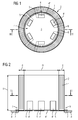
- an electrical circuit arrangement has a first capacitor 1.
- the first capacitor 1 is part of a first capacitor arrangement 2, which surrounds a cavity 3 in an annular manner.
- the first capacitor 1 is preferably designed as a wound capacitor. Winding capacitors are generally known in particular in the form of film capacitors and electrolytic capacitors.
- the first capacitor arrangement 2 may for example have an inner diameter D which is between 8 cm and 50 cm.
- the first capacitor arrangement 2 further has a height H which, for example, likewise lies between 8 cm and 50 cm.
- a wall thickness d is usually at least 5 mm and can be up to 3 cm. In individual cases, however, it is possible to deviate from these values.
- the further circuit part 4 is preferably - but not necessarily - constructed radially symmetrical or has seen in the circumferential direction at least a certain periodicity.
- connection of the contact tabs 5 with the first capacitor 1 may be sufficient to cause the mechanical support of the further circuit part 4.
- the first capacitor arrangement 2 furthermore has fastening elements 7.
- the fastening elements 7 By means of the fastening elements 7, the first capacitor arrangement 2 and with it preferably at the same time also the electrical circuit arrangement as a whole mechanically fastened to a holding element 8.
- the attachment can, for example, over in FIG. 2 schematically indicated screw 9 done.
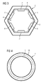
- the first capacitor arrangement 2 is designed as a hollow cylinder.
- the first capacitor arrangement 2 forms in cross-section a convex, curved curve.
- Alternatives to a circle are, for example, an ellipse or a Oval.
- These embodiments offer manufacturing advantages.
- the first capacitor arrangement as shown in FIG. 3 form a polygon in cross section.
- this refinement offers the advantage that the components 4 'can rest flat against the wall 4.
- the curvature of the first capacitor assembly 2 on its inside as shown in FIG FIG. 1 cause circumstances that the components 4 'contact the wall 6 only at their edges.
- the areal contact can also be advantageous, for example, for cooling the components 4 '.
- Other contacts, such as soldering and bonding can be easier to implement.
- the corners of the polygon are preferably rounded off. This offers over sharp corners in particular manufacturing advantages. Also, for reasons of design, this embodiment may be advantageous. Furthermore, in the case of the embodiment as a polygon, the number of corners is preferably between three and twelve, in particular between five and ten. For example, as shown in FIG. 3 lie at six.
- the 1 to 3 show the simplest embodiment in which the first capacitor arrangement 2 except for the first capacitor 1 contains no further capacitor.
- the first capacitor arrangement 2 has a further capacitor 10 which surrounds the first capacitor 1 radially outward.
- the further capacitor 10 is referred to below as the second capacitor 10.
- the second capacitor 10 is - at least preferably - formed as a wound capacitor.
- the first capacitor arrangement 2 - this is neither in FIG. 4 still shown in the other FIG - include even more capacitors. The capacitors follow in this case, radially (ie viewed from the cavity from inside to outside or vice versa) sequentially to each other.
- the further circuit part 4 For contacting the further circuit part 4 with the first capacitor 1 (and optionally the other capacitors 10 of the first capacitor arrangement 2), various embodiments are possible. In conjunction with the 1 and 2 has already been explained an embodiment in which for this purpose the contact tabs 5 are present.
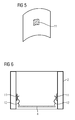
- the first capacitor arrangement 2 as shown in FIGS FIGS. 5 and 6 have contact elements 11 on their inner side facing the cavity 3.
- the contact elements 11 may be formed, for example, as contact fields. Shown in FIG. 5 a single contact element 11 and in FIG. 6 two contact elements 11. In this case - ie in the case of the presence of contact elements 11 - the first capacitor 1 of the further circuit part 4 via the contact elements 11 is electrically contacted.
- the further circuit part 4 (the in FIG. 5 not shown with and in FIG.
- spring contacts 12 which are pressed against the contact elements 11 and thereby contact the contact elements 11 electrically.
- the contact elements 11 can be recessed in the wall 6 or be surrounded by a peripheral edge. In these two cases - depending on the spring force of the spring contacts 12 - by the spring contacts 12 and a sufficiently stable mechanical connection of the other circuit part 4 can be achieved.
- the first capacitor arrangement 2 has contact points 14 at its abutment surfaces 13.
- the first capacitor 1 can be electrically contacted by the further circuit part 4 via the contact points 14.
- the contact points 14, for example, in the already in connection with the 1 and 2 pass over mentioned contact tabs 5.
- the first capacitor arrangement 2 on its abutment surfaces 13 pins and / or sockets for receiving connector pins. Other embodiments are possible.
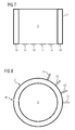
- FIG. 8 shows two further embodiments of the first capacitor arrangement 2. These two embodiments are independent of each other feasible. Furthermore, these two embodiments can be realized in each of the previously explained embodiments.
- the first capacitor arrangement 2 has cooling surfaces 15 on its outside.
- the cooling surfaces 15 protrude radially outward, ie away from the first capacitor arrangement 2.
- the direction in which the cooling surfaces 15 extend may in this case have a slight tangential component (ie around the first capacitor arrangement 2) and / or a slight axial component.
- the first capacitor arrangement 2 has a concave-convex contour in cross-section. This is in contrast to a design without cooling surfaces. In this case, the first capacitor arrangement 2 would have a purely convex contour seen in cross-section.
- the first capacitor arrangement 2 according to FIG. 8 a predetermined breaking point 16.
- the circuit arrangement may be formed as needed.
- the circuit arrangement as shown in FIG. 9 be designed as a DC link converter.
- the DC link converter is supplied in this case via a rectifier 17, an AC voltage.
- the supplied AC voltage can be as shown in FIG. 9 be multi-phase. Alternatively, it may be a single-phase AC voltage.
- the rectifier 17 may alternatively be an uncontrolled rectifier (diode rectifier) or a controlled and thus regenerative rectifier.
- From the DC link converter is also output via an inverter 18, an AC voltage.
- the output AC voltage can - analogous to the supplied AC voltage - accordingly the representation in FIG. 9 be multi-phase.
- it may be a single-phase AC voltage.
- an intermediate circuit capacitor 19 is arranged between the rectifier 17 and the inverter 18 is further, as is common practice.
- the further circuit part 4 may in particular comprise the rectifier 17.
- the further circuit part 4 may include the inverter 18.
- the further circuit part 4 may include both the rectifier 17 and the inverter 18.
- the components 4 'of the further circuit part 4 can correspond to the semiconductor switches of the rectifier 17 and / or of the inverter 18.
- the first capacitor 1 may in particular be the DC link capacitor or be part of the DC link capacitor.
- an embodiment of the first capacitor arrangement 2 offers a polygon with three, four, five, six, eight, ten or twelve corners.
- An embodiment with three corners, not shown in the figures, is suitable, for example, if both the supplied and the emitted alternating voltage are three-phase and full bridge rectification and full bridge alternating direction occur.
- two further circuit parts 4 may be present, one of which each comprises the rectifier 17 and the inverter 18 and on each side of the polygon two semiconductor switches are arranged.
- the two circuit parts 4 are arranged in this case in different levels of the cavity 3.
- four semiconductor switches may be arranged in a single plane on each side of the polygon.
- An embodiment with four corners is useful, for example, if both the supplied and the delivered AC voltage are single phase and a full bridge rectification and a full bridge alternating direction.
- two further circuit parts 4 may be present, of which one each comprises the rectifier 17 and the inverter 18.
- the two circuit parts 4 are in this case, as in FIG. 10 indicated schematically, arranged in different levels of the cavity 3.
- two semiconductor switches may be arranged in a single plane on each side of the polygon.
- An embodiment with five corners is suitable, for example, when the supplied AC voltage is single-phase, the AC voltage output is three-phase and a full bridge rectification and a full bridge alternating direction take place.
- two further circuit parts 4 may be present, each comprising two semiconductor switches of the rectifier 17 and three semiconductor switches of the inverter 18.
- the two circuit parts 4 are also in this case, analogous to FIG. 10 , arranged in different levels of the cavity 3.
- An analogous embodiment is possible if conversely the supplied AC voltage is three-phase, the AC voltage output is single-phase and a full-bridge rectification and a full-bridge alternating direction take place.
- two semiconductor switches may be arranged in a single plane on each side of the polygon.
- An embodiment with six corners is suitable, for example, if both the supplied and the discharged alternating voltage are three-phase and full bridge rectification and a full bridge alternating direction take place.
- two further circuit parts 4 may be present, of which one each comprises the rectifier 17 and the inverter 18.
- the two circuit parts 4 are in this case, analogous to FIG. 10 , arranged in different levels of the cavity 3.
- two semiconductor switches may be arranged in a single plane on each side of the polygon.
- a single circuit part 4 may be present, which includes both the rectifier 17 and the inverter 18.
- the circuit part 4 is in this case, analogous to the representation in FIG FIG. 2 , arranged in a single plane of the cavity 3.
- An embodiment with ten corners is suitable, for example, when the supplied AC voltage is single-phase, the AC voltage output is three-phase and a full-bridge rectification and a full-bridge alternating direction take place.
- a single circuit part 4 may be present, which includes both the rectifier 17 and the inverter 18.
- the circuit part 4 is in this case, analogous to the representation in FIG FIG. 2 , arranged in a single plane of the cavity 3.
- An analogous embodiment is possible if conversely the supplied AC voltage is three-phase, the AC voltage output is single-phase and a full-bridge rectification and a full-bridge alternating direction take place.
- a single circuit part 4 may be present, which includes both the rectifier 17 and the inverter 18.
- the circuit part 4 is in this case, analogous to the representation in FIG FIG. 2 , arranged in a single plane of the cavity 3.
- a single capacitor arrangement - namely the first capacitor arrangement 2 - several capacitors 1, 10 may have.
- a second capacitor arrangement 19 has.
- the second capacitor arrangement 19 in turn has at least one capacitor 20, hereinafter referred to as a further capacitor 20.
- the further capacitor 20 also interacts electrically with the circuit part 4.
- the further circuit part 4 is electrically connected to the other capacitor 20 for this purpose.
- the connection to the further capacitor 20 can be realized either directly or indirectly via the first capacitor arrangement 2.
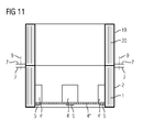
- the second capacitor arrangement 19 surrounds the cavity 3 in an annular manner.
- the second capacitor arrangement 19 is as shown in FIG FIG. 11 placed on the first capacitor assembly 2 and fixed with this.
- the present invention thus relates to the following facts:
- An electrical circuit arrangement has at least one first capacitor 1 and at least one further, with the first capacitor 1 electrically cooperating circuit part 4.
- the first capacitor 1 is part of a first capacitor arrangement 2, which surrounds a cavity 3 in an annular manner.
- the further circuit part 4 is at least partially disposed within the cavity 3 and electrically connected to the first capacitor 1.
- the first capacitor arrangement 2 has fastening elements 7, by means of which the circuit arrangement can be fastened mechanically to a holding element 8.
- the present invention has many advantages.
- the first capacitor 1 can be arranged very close to the components 4 '.
- a line length can therefore be minimized.
- this results in low intrinsic inductances of connecting lines.
- This statement also applies analogously to the second capacitors 10 and the capacitors 20 of the second capacitor arrangement 19.
- High capacitances in the immediate vicinity of switching elements (components 4 ') can be realized.
- the first capacitor arrangement 2 is easy to manufacture in winding technology. By integrating the housing function in the first capacitor arrangement 2 (and optionally further capacitor arrangements 19) additional components and thus costs and installation space can be saved. Due to the large surface area of the first capacitor arrangement 2, it can be cooled well.
- the first capacitor arrangement 2 has a high intrinsic stability and is therefore able to mechanically hold and support the further circuit part 4.
- the provision of a predetermined breaking point 16 makes it possible to specifically protect the environment of the circuit arrangement or the circuit arrangement itself against a danger from a defect of the first capacitor 1 (or of another capacitor 10 of the capacitor arrangement 2).
- the inventive design also improves the EMC properties of the circuit arrangement at the same time. If necessary, a plurality of capacitor assemblies 1, 19 - possibly also with different design, size and capacity - can be electrically and mechanically coupled. The size and the capacity can thus be scaled as required. It is even possible to connect the capacitor arrangements 1, 19 exclusively mechanically with one another, so that independently connectable capacitors 1, 10, 20 are available.
Landscapes
- Engineering & Computer Science (AREA)
- Power Engineering (AREA)
- Microelectronics & Electronic Packaging (AREA)
- Manufacturing & Machinery (AREA)
- Inverter Devices (AREA)
Priority Applications (6)
| Application Number | Priority Date | Filing Date | Title |
|---|---|---|---|
| EP15186521.9A EP3148303A1 (de) | 2015-09-23 | 2015-09-23 | Elektrische schaltungsanordnung mit kondensator mit gehäusefunktion |
| US15/762,451 US10306794B2 (en) | 2015-09-23 | 2016-08-08 | Electrical circuit arrangement having a capacitor with a housing function |
| PCT/EP2016/069386 WO2017050489A1 (de) | 2015-09-23 | 2016-08-16 | Elektrische schaltungsanordnung mit kondensator mit gehäusefunktion |
| EP16751596.4A EP3329753B1 (de) | 2015-09-23 | 2016-08-16 | Elektrische schaltungsanordnung mit kondensator mit gehäusefunktion |
| JP2018515223A JP6516927B2 (ja) | 2015-09-23 | 2016-08-16 | ハウジング機能を持つコンデンサを有する電気回路装置 |
| CN201680049381.XA CN108141985B (zh) | 2015-09-23 | 2016-08-16 | 具有带有壳体功能的电容器的电路装置 |
Applications Claiming Priority (1)
| Application Number | Priority Date | Filing Date | Title |
|---|---|---|---|
| EP15186521.9A EP3148303A1 (de) | 2015-09-23 | 2015-09-23 | Elektrische schaltungsanordnung mit kondensator mit gehäusefunktion |
Publications (1)
| Publication Number | Publication Date |
|---|---|
| EP3148303A1 true EP3148303A1 (de) | 2017-03-29 |
Family
ID=54238242
Family Applications (2)
| Application Number | Title | Priority Date | Filing Date |
|---|---|---|---|
| EP15186521.9A Withdrawn EP3148303A1 (de) | 2015-09-23 | 2015-09-23 | Elektrische schaltungsanordnung mit kondensator mit gehäusefunktion |
| EP16751596.4A Active EP3329753B1 (de) | 2015-09-23 | 2016-08-16 | Elektrische schaltungsanordnung mit kondensator mit gehäusefunktion |
Family Applications After (1)
| Application Number | Title | Priority Date | Filing Date |
|---|---|---|---|
| EP16751596.4A Active EP3329753B1 (de) | 2015-09-23 | 2016-08-16 | Elektrische schaltungsanordnung mit kondensator mit gehäusefunktion |
Country Status (5)
| Country | Link |
|---|---|
| US (1) | US10306794B2 (OSRAM) |
| EP (2) | EP3148303A1 (OSRAM) |
| JP (1) | JP6516927B2 (OSRAM) |
| CN (1) | CN108141985B (OSRAM) |
| WO (1) | WO2017050489A1 (OSRAM) |
Cited By (1)
| Publication number | Priority date | Publication date | Assignee | Title |
|---|---|---|---|---|
| WO2020025884A1 (fr) * | 2018-07-31 | 2020-02-06 | Safran | Machine electrique polyphasee a electronique de puissance integree et a circuit de refroidissement integre |
Citations (4)
| Publication number | Priority date | Publication date | Assignee | Title |
|---|---|---|---|---|
| DE4443498C1 (de) * | 1994-12-07 | 1996-02-15 | Export Contor Ausenhandelsgese | Dynamisch angesteuerter Motor |
| US20090231812A1 (en) * | 2008-03-17 | 2009-09-17 | Wiles Randy H | Direct cooled power electronics substrate |
| US20100321859A1 (en) * | 2007-11-01 | 2010-12-23 | Sbelectronics Inc. | Annular Capacitor with power conversion components arranged and attached in manners uniquely allowed by the ring shaped form factor |
| EP2672618A1 (en) * | 2012-06-04 | 2013-12-11 | ABB Oy | Modular motor inverter arrangement with cooling sections forming inner duct ring capacitor on the outside |
Family Cites Families (11)
| Publication number | Priority date | Publication date | Assignee | Title |
|---|---|---|---|---|
| WO1987004892A1 (fr) * | 1986-02-06 | 1987-08-13 | Fujitsu Limited | Structure de mise a la terre d'une carte de circuits imprimes a noyau metallique |
| JPH0719991B2 (ja) * | 1990-02-28 | 1995-03-06 | 三菱電機株式会社 | 制御装置ケース |
| US5920984A (en) * | 1993-12-10 | 1999-07-13 | Ericsson Ge Mobile Communications Inc. | Method for the suppression of electromagnetic interference in an electronic system |
| JPH0831691A (ja) | 1994-07-12 | 1996-02-02 | Marcon Electron Co Ltd | 円筒形shコンデンサ |
| DE19846156C1 (de) | 1998-10-07 | 2000-07-27 | Bosch Gmbh Robert | Anordnung eines mehrphasigen Umrichters |
| SE515900C2 (sv) * | 2000-01-14 | 2001-10-22 | Abb Ab | Kraftkondensator och användning och förfarande vid sådan |
| SE515883C2 (sv) * | 2000-01-14 | 2001-10-22 | Abb Ab | Kraftkondensator, kondensatorbatteri samt användning av en eller flera kraftkondensatorer |
| DE102004048908A1 (de) * | 2004-10-06 | 2006-04-20 | Daimlerchrysler Ag | Antriebsstrang für ein Fahrzeug mit elektrischer Maschine |
| WO2010049764A1 (en) | 2008-10-30 | 2010-05-06 | Sawyer, Ed | Annular capacitor with power conversion components |
| AT14177U1 (de) | 2013-06-27 | 2015-05-15 | Secop Austria Gmbh | Elektrischer Kondensator für Kältemittelverdichter |
| DE112015004606T5 (de) * | 2014-10-08 | 2017-07-06 | Remy Technologies, Llc | Sockelfläche für MOSFET Modul |
-
2015
- 2015-09-23 EP EP15186521.9A patent/EP3148303A1/de not_active Withdrawn
-
2016
- 2016-08-08 US US15/762,451 patent/US10306794B2/en active Active
- 2016-08-16 CN CN201680049381.XA patent/CN108141985B/zh active Active
- 2016-08-16 JP JP2018515223A patent/JP6516927B2/ja active Active
- 2016-08-16 WO PCT/EP2016/069386 patent/WO2017050489A1/de not_active Ceased
- 2016-08-16 EP EP16751596.4A patent/EP3329753B1/de active Active
Patent Citations (4)
| Publication number | Priority date | Publication date | Assignee | Title |
|---|---|---|---|---|
| DE4443498C1 (de) * | 1994-12-07 | 1996-02-15 | Export Contor Ausenhandelsgese | Dynamisch angesteuerter Motor |
| US20100321859A1 (en) * | 2007-11-01 | 2010-12-23 | Sbelectronics Inc. | Annular Capacitor with power conversion components arranged and attached in manners uniquely allowed by the ring shaped form factor |
| US20090231812A1 (en) * | 2008-03-17 | 2009-09-17 | Wiles Randy H | Direct cooled power electronics substrate |
| EP2672618A1 (en) * | 2012-06-04 | 2013-12-11 | ABB Oy | Modular motor inverter arrangement with cooling sections forming inner duct ring capacitor on the outside |
Cited By (3)
| Publication number | Priority date | Publication date | Assignee | Title |
|---|---|---|---|---|
| WO2020025884A1 (fr) * | 2018-07-31 | 2020-02-06 | Safran | Machine electrique polyphasee a electronique de puissance integree et a circuit de refroidissement integre |
| FR3084791A1 (fr) * | 2018-07-31 | 2020-02-07 | Safran | Machine electrique polyphasee a electronique de puissance integree |
| US11764652B2 (en) | 2018-07-31 | 2023-09-19 | Safran | Polyphased electrical machine with integrated power electronics and an integrated coolant circuit |
Also Published As
| Publication number | Publication date |
|---|---|
| US10306794B2 (en) | 2019-05-28 |
| CN108141985B (zh) | 2019-05-10 |
| US20180270979A1 (en) | 2018-09-20 |
| JP2018528754A (ja) | 2018-09-27 |
| WO2017050489A1 (de) | 2017-03-30 |
| CN108141985A (zh) | 2018-06-08 |
| EP3329753A1 (de) | 2018-06-06 |
| JP6516927B2 (ja) | 2019-05-22 |
| EP3329753B1 (de) | 2019-12-18 |
Similar Documents
| Publication | Publication Date | Title |
|---|---|---|
| EP3707737B1 (de) | Leistungselektronikeinrichtung | |
| DE102020104001A1 (de) | Sammelschienenvorrichtung, motor, und verfahren zum herstellen einer sammelschienenvorrichtung | |
| DE112008002974T5 (de) | Massenanschlussfahne und Erdungsvorrichtung hiermit | |
| DE102015225088A1 (de) | Motor und Verfahren zum Herstellen desselben | |
| EP3096336B1 (de) | Induktives bauelement für leiterplattenmontage und wechselrichter mit einem leiterplattenmontierten induktiven bauelement | |
| DE102009015542A1 (de) | Bidirektionale Kabelschuhverbindung und Verfahren | |
| DE112016003644T5 (de) | Stator und Motor | |
| DE102015105347A1 (de) | Anordnung mit einem leitstungselektronischen Bauteil und mit einer Gleichspannungsverschienung | |
| EP4154286B1 (de) | Kondensatoranordnung, fahrzeugantriebs-leistungselektronikvorrichtung mit einer kondensatoranordnung | |
| DE102019124246A1 (de) | Elektrischer Verteilerkasten | |
| DE102007027459A1 (de) | Klemmenbrett | |
| WO2016102057A1 (de) | Elektronikbaueinheit für einen elektromotor eines einzelradantriebs eines kraftfahrzeugs, einzelradantrieb sowie kraftfahrzeug | |
| EP3329753B1 (de) | Elektrische schaltungsanordnung mit kondensator mit gehäusefunktion | |
| DE102017129707A1 (de) | Verfahren zur Herstellung eines leistungselektronischen Systems | |
| DE102012018086A1 (de) | Stromschienenanordnung | |
| DE202014003844U1 (de) | Verschaltungsanordnung und Stator mit einer Verschaltungsanordnung | |
| DE102013005327A1 (de) | Überspannungsschutzanordnung mit scheibenförmigem Varistor | |
| DE102017111675A1 (de) | Bürstenloser Gleichstrommotor, Ständerteil und Wicklungsverfahren davon | |
| DE102016225291A1 (de) | Entkopplungselement zur Verbindung einer Leistungselektronik mit einer elektrischen Maschine | |
| EP3240380B1 (de) | Umrichteranordnung | |
| DE112017002164B4 (de) | Leitungsweg mit Rauschfilter | |
| EP1256965B1 (de) | Kondensator | |
| EP4010940B1 (de) | Dichtung für ein batteriegehäuse einer hochvoltbatterie, verfahren, batteriegehäuse, hochvoltbatterie sowie kraftfahrzeug | |
| DE102021128835B4 (de) | Schaltungsanordnung mit flächig aufgebrachtem Kondensator | |
| EP3479387B1 (de) | Spannungswandlereinheit mit einem aktivteilgehäuse |
Legal Events
| Date | Code | Title | Description |
|---|---|---|---|
| PUAI | Public reference made under article 153(3) epc to a published international application that has entered the european phase |
Free format text: ORIGINAL CODE: 0009012 |
|
| AK | Designated contracting states |
Kind code of ref document: A1 Designated state(s): AL AT BE BG CH CY CZ DE DK EE ES FI FR GB GR HR HU IE IS IT LI LT LU LV MC MK MT NL NO PL PT RO RS SE SI SK SM TR |
|
| AX | Request for extension of the european patent |
Extension state: BA ME |
|
| RAP1 | Party data changed (applicant data changed or rights of an application transferred) |
Owner name: SIEMENS AKTIENGESELLSCHAFT |
|
| STAA | Information on the status of an ep patent application or granted ep patent |
Free format text: STATUS: THE APPLICATION IS DEEMED TO BE WITHDRAWN |
|
| 18D | Application deemed to be withdrawn |
Effective date: 20170930 |