EP3145068A1 - Compensation network, switch power supply circuit and circuit compensation method - Google Patents
Compensation network, switch power supply circuit and circuit compensation method Download PDFInfo
- Publication number
- EP3145068A1 EP3145068A1 EP14892037.4A EP14892037A EP3145068A1 EP 3145068 A1 EP3145068 A1 EP 3145068A1 EP 14892037 A EP14892037 A EP 14892037A EP 3145068 A1 EP3145068 A1 EP 3145068A1
- Authority
- EP
- European Patent Office
- Prior art keywords
- network
- resistor
- pole
- capacitor
- amplifier
- Prior art date
- Legal status (The legal status is an assumption and is not a legal conclusion. Google has not performed a legal analysis and makes no representation as to the accuracy of the status listed.)
- Withdrawn
Links
Images
Classifications
-
- H—ELECTRICITY
- H02—GENERATION; CONVERSION OR DISTRIBUTION OF ELECTRIC POWER
- H02M—APPARATUS FOR CONVERSION BETWEEN AC AND AC, BETWEEN AC AND DC, OR BETWEEN DC AND DC, AND FOR USE WITH MAINS OR SIMILAR POWER SUPPLY SYSTEMS; CONVERSION OF DC OR AC INPUT POWER INTO SURGE OUTPUT POWER; CONTROL OR REGULATION THEREOF
- H02M3/00—Conversion of dc power input into dc power output
- H02M3/02—Conversion of dc power input into dc power output without intermediate conversion into ac
- H02M3/04—Conversion of dc power input into dc power output without intermediate conversion into ac by static converters
- H02M3/10—Conversion of dc power input into dc power output without intermediate conversion into ac by static converters using discharge tubes with control electrode or semiconductor devices with control electrode
- H02M3/145—Conversion of dc power input into dc power output without intermediate conversion into ac by static converters using discharge tubes with control electrode or semiconductor devices with control electrode using devices of a triode or transistor type requiring continuous application of a control signal
- H02M3/155—Conversion of dc power input into dc power output without intermediate conversion into ac by static converters using discharge tubes with control electrode or semiconductor devices with control electrode using devices of a triode or transistor type requiring continuous application of a control signal using semiconductor devices only
- H02M3/156—Conversion of dc power input into dc power output without intermediate conversion into ac by static converters using discharge tubes with control electrode or semiconductor devices with control electrode using devices of a triode or transistor type requiring continuous application of a control signal using semiconductor devices only with automatic control of output voltage or current, e.g. switching regulators
-
- H—ELECTRICITY
- H02—GENERATION; CONVERSION OR DISTRIBUTION OF ELECTRIC POWER
- H02M—APPARATUS FOR CONVERSION BETWEEN AC AND AC, BETWEEN AC AND DC, OR BETWEEN DC AND DC, AND FOR USE WITH MAINS OR SIMILAR POWER SUPPLY SYSTEMS; CONVERSION OF DC OR AC INPUT POWER INTO SURGE OUTPUT POWER; CONTROL OR REGULATION THEREOF
- H02M1/00—Details of apparatus for conversion
- H02M1/44—Circuits or arrangements for compensating for electromagnetic interference in converters or inverters
-
- G—PHYSICS
- G05—CONTROLLING; REGULATING
- G05F—SYSTEMS FOR REGULATING ELECTRIC OR MAGNETIC VARIABLES
- G05F1/00—Automatic systems in which deviations of an electric quantity from one or more predetermined values are detected at the output of the system and fed back to a device within the system to restore the detected quantity to its predetermined value or values, i.e. retroactive systems
- G05F1/10—Regulating voltage or current
- G05F1/46—Regulating voltage or current wherein the variable actually regulated by the final control device is dc
- G05F1/56—Regulating voltage or current wherein the variable actually regulated by the final control device is dc using semiconductor devices in series with the load as final control devices
- G05F1/575—Regulating voltage or current wherein the variable actually regulated by the final control device is dc using semiconductor devices in series with the load as final control devices characterised by the feedback circuit
-
- H—ELECTRICITY
- H02—GENERATION; CONVERSION OR DISTRIBUTION OF ELECTRIC POWER
- H02M—APPARATUS FOR CONVERSION BETWEEN AC AND AC, BETWEEN AC AND DC, OR BETWEEN DC AND DC, AND FOR USE WITH MAINS OR SIMILAR POWER SUPPLY SYSTEMS; CONVERSION OF DC OR AC INPUT POWER INTO SURGE OUTPUT POWER; CONTROL OR REGULATION THEREOF
- H02M3/00—Conversion of dc power input into dc power output
- H02M3/02—Conversion of dc power input into dc power output without intermediate conversion into ac
- H02M3/04—Conversion of dc power input into dc power output without intermediate conversion into ac by static converters
-
- H—ELECTRICITY
- H03—ELECTRONIC CIRCUITRY
- H03F—AMPLIFIERS
- H03F1/00—Details of amplifiers with only discharge tubes, only semiconductor devices or only unspecified devices as amplifying elements
- H03F1/08—Modifications of amplifiers to reduce detrimental influences of internal impedances of amplifying elements
- H03F1/083—Modifications of amplifiers to reduce detrimental influences of internal impedances of amplifying elements in transistor amplifiers
-
- H—ELECTRICITY
- H03—ELECTRONIC CIRCUITRY
- H03F—AMPLIFIERS
- H03F3/00—Amplifiers with only discharge tubes or only semiconductor devices as amplifying elements
- H03F3/45—Differential amplifiers
- H03F3/45071—Differential amplifiers with semiconductor devices only
- H03F3/45076—Differential amplifiers with semiconductor devices only characterised by the way of implementation of the active amplifying circuit in the differential amplifier
- H03F3/45475—Differential amplifiers with semiconductor devices only characterised by the way of implementation of the active amplifying circuit in the differential amplifier using IC blocks as the active amplifying circuit
-
- H—ELECTRICITY
- H02—GENERATION; CONVERSION OR DISTRIBUTION OF ELECTRIC POWER
- H02M—APPARATUS FOR CONVERSION BETWEEN AC AND AC, BETWEEN AC AND DC, OR BETWEEN DC AND DC, AND FOR USE WITH MAINS OR SIMILAR POWER SUPPLY SYSTEMS; CONVERSION OF DC OR AC INPUT POWER INTO SURGE OUTPUT POWER; CONTROL OR REGULATION THEREOF
- H02M1/00—Details of apparatus for conversion
- H02M1/0003—Details of control, feedback or regulation circuits
-
- H—ELECTRICITY
- H03—ELECTRONIC CIRCUITRY
- H03F—AMPLIFIERS
- H03F2203/00—Indexing scheme relating to amplifiers with only discharge tubes or only semiconductor devices as amplifying elements covered by H03F3/00
- H03F2203/45—Indexing scheme relating to differential amplifiers
- H03F2203/45526—Indexing scheme relating to differential amplifiers the FBC comprising a resistor-capacitor combination and being coupled between the LC and the IC
Definitions
- the present invention relates to the field of microelectronic technologies, and particularly to a compensation network, a switching power supply circuit and a circuit compensation method.
- Power supply technology belongs to a category of power electronic technology, and is an edge cross subject integrating many disciplines, such as power conversion, modem electronics and automatic control, and has been widely applied in various fields nowadays, such as industry, energy sources, traffic, IT, aeronautics, national defense, education, and culture.
- development of the power supply technology is concentrated on diligent studies conducted for improving an efficiency and a performance, reducing in size and weight, being safe and reliable, eliminating power public nuisance, and reducing electromagnetic interference and traces of electric noise, a switching power supply is a crucial part in the whole power supply technology, where, a compensation network of a Pulse Width Modulation (PWM) power supply regulator is an important research subject of the switching power supply.
- PWM Pulse Width Modulation
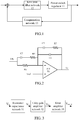
- a switching power supply circuit is composed of three basic modules, as shown in FIG. 1 , which include: a power switching regulator 11, a low pass filter network 12 and a compensation network 13.
- the power switching regulator 11 is configured to generate a square wave signal, to control an ON/OFF state of a power tube;
- the low pass filter network 12, i.e., an LC network is configured to filter an output voltage and current, to generate an LC double pole;
- the compensation network 13 is composed of a voltage sampling circuit, an error amplifier and a compensation circuit element.
- An error amplifier is often used in design of a switching power supply circuit, if a low-frequency gain desired by the switching power supply circuit is very high, there is a need to compensate the error amplifier in the compensation network, so as to guarantee that the switching power supply circuit has a great bandwidth and a good phase margin.
- a high low-frequency gain is required by the switching power supply circuit in a voltage mode, but a power-stage transfer function has a low low-frequency gain, and there is a pair of LC conjugated poles, therefore there is a need to add an error amplifier to obtain a high low-frequency gain and meanwhile compensate the error amplifier to eliminate influence of the conjugated poles, so as to make the switching power supply circuit have a high phase margin at the same time of obtaining a great bandwidth.
- a conventional compensation network adopts a solution that two ends of an error amplifier AMP0 are bridged with resistance capacitance networks, and the compensation network composed of resistors R6, R7, R8 and capacitors C5, C6, C7 just can compensate three poles and two zeros in the original switching power supply circuit.
- the switching power supply circuit obtained in such way can obtain a high bandwidth and phase margin at a low frequency, have a small gain at a switching frequency, and thus have a good suppression effect on switching noises.
- a switching frequency required by the switching power supply circuit is high, stability of the switching power supply circuit cannot be guaranteed any more due to a pole effect of the error amplifier itself.
- a pole would also be introduced when an input end of the error amplifier needs to be connected with a voltage dividing resistor, which has a great effect on compensation.
- embodiments of the present invention provide a compensation network, a switching power supply circuit and a circuit compensation method.
- Embodiments of the present invention provide a compensation network, including: a resistance capacitance network, a unity gain amplifier network and an error amplifier network; where, an output end of the resistance capacitance network is cascaded to an input end of the unity gain amplifier network, and an output end of the unity gain amplifier network is cascaded to an input end of the error amplifier network; the resistance capacitance network is configured to provide a voltage dividing resistor, and generate a zero and a pole which are mutually canceled; the unity gain amplifier network is configured to generate a zero for canceling a pole in a low pass filter network, and a pole for suppressing a high-frequency noise and improving a phase margin of a switching power supply circuit; and the error amplifier network is configured to generate a pole for increasing low-frequency gain and a zero for canceling another pole in the low pass filter network.
- the resistance capacitance network includes: a first resistor, a second resistor, a first capacitor and a second capacitor; where, the first resistor is connected in series between a first input end and a first output end, the second capacitor is connected between two ends of the first resistor, the first capacitor is connected between the first input end and the ground, and the second resistor is connected between the first output end and the ground.
- the unity gain amplifier network includes: a first amplifier, a third resistor, a fourth resistor and a third capacitor; where, the third resistor is connected between an inverting input end and an output end of the first amplifier; the fourth resistor and the third capacitor is connected between the inverting input end of the first amplifier and the ground; a positive input end of the first amplifier is connected to the first output end of the resistance capacitance network.
- the error amplifier network includes: a second amplifier, a fifth resistor and a fourth capacitor; where, the fifth resistor and the fourth capacitor is connected between an output end of the second amplifier and the ground; a positive input end of the second amplifier is connected to an output end of the unity gain amplifier network.
- the second capacitor is a variable capacitor
- the first resistor and the second resistor are variable resistors.
- the third capacitor is a variable capacitor
- the third resistor and the fourth resistor are variable resistors.
- the fourth capacitor is a variable capacitor
- the fifth resistor is a variable resistor
- a capacitance value of the fourth capacitor is far greater than an equivalent capacitance value of the second amplifier.
- Embodiments of the present invention provide a switching power supply circuit, including the compensation network described above.
- Embodiments of the present invention provide a circuit compensation method, including: a resistance capacitance network provides a voltage dividing resistor and generates a zero and a pole which are mutually canceled; a unity gain amplifier network generates a zero for canceling a pole in a low pass filter network, and a pole for suppressing a high-frequency noise and improving a phase margin of a switching power supply circuit; and an error amplifier network generates a pole for increasing low-frequency gain and a zero for canceling another pole in the low pass filter network.
- the compensation network includes: a resistance capacitance network, a unity gain amplifier network and an error amplifier network; where, an output end of the resistance capacitance network is cascaded to an input end of the unity gain amplifier network, and an output end of the unity gain amplifier network is cascaded to an input end of the error amplifier network; the resistance capacitance network is configured to provide a voltage dividing resistor, and generate a zero and a pole which are mutually canceled; the unity gain amplifier network is configured to isolate a dividing resistor and the error amplifier network, transfer a voltage change in an input end to an output end of the error amplifier network, generate a zero for canceling a pole in a low pass filter network, and a pole for suppressing a high-frequency noise and improving a phase margin of a switching power supply circuit; and the error amplifier network is configured to output the amplified voltage change, and generate a pole for increasing low-frequency gain and a zero for canceling another pole in the low pass filter network.
- the switching power supply circuit can have a good phase margin at the same time of obtaining a very high bandwidth.
- Embodiments of the present invention provide a compensation network, including: a resistance capacitance network, a unity gain amplifier network and an error amplifier network; where an output end of the resistance capacitance network is cascaded to an input end of the unity gain amplifier network, and an output end of the unity gain amplifier network is cascaded to an input end of the error amplifier network; the resistance capacitance network is configured to provide a voltage dividing resistor, and generate a zero and a pole which are mutually canceled; the unity gain amplifier network is configured to generate a zero for canceling a pole in a low pass filter network, and a pole for suppressing a high-frequency noise and improving a phase margin of a switching power supply circuit; the error amplifier network is configured to generate a pole for increasing low-frequency gain and a zero for canceling another pole in the low pass filter network.
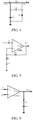
- FIG. 3 is a schematic structural diagram illustrating the compensation network, as shown in FIG. 3 , the compensation network is composed of three-stage compensation networks, which respectively are: a resistance capacitance network 31, a unity gain amplifier network 32 and an error amplifier network 33; an output end of the resistance capacitance network 31 is cascaded to an input end of the unity gain amplifier network 32, and an output end of the unity gain amplifier network 32 is cascaded to an input end of the error amplifier network 33; therefore, a voltage V 1 is output after an output voltage V in of the switching power supply is input into the resistance capacitance network 31, a voltage V 2 is output after the voltage V 1 is input into the unity gain amplifier network 32, and an output voltage V eaout is generated after the voltage V 2 enters the error amplifier network 33; where, the resistance capacitance network 31 is configured to provide a voltage dividing resistor, and generate a zero and a pole which are mutually canceled; the unity gain amplifier network 32 is configured to isolate the dividing resist
- FIG. 4 is a basic schematic structural diagram illustrating a resistance capacitance network in a compensation network according to an embodiment of the present invention, as shown in FIG. 4 , the resistance capacitance network is composed of a first resistor R1, a second resistor R2, a first capacitor C 1 and a second capacitor C2; the first resistor R1 and the second resistor R2 are voltage dividing resistors; the first resistor R1 is connected in series between a first input end A and a first output end B, the second capacitor C2 is connected between two ends of the first resistor R1; the C1 is connected between the first input end A and the ground, so as to stable input; the second resistor R2 is connected between the first output end B and the ground; it should be noted that, the first resistor R1 and the second resistor R2 may be variable resistors, the first capacitor C 1 and the second capacitor C2 may be variable capacitors; assuming that the output voltage V in of the switching power supply circuit is input after sampling or directly from the first input end A of the resistance capac
- a zero and a pole are introduced when the resistance capacitance network provides the voltage dividing resistor for the compensation network, as such, the zero and the pole are mutually canceled, which will not affect the compensation network, unlike in the prior art that one pole is introduced when an input end of the error amplifier is connected to a voltage dividing resistor, which affects compensation effect to the compensation network.
- FIG. 5 is a basic schematic structural diagram illustrating a unity gain amplifier network in a compensation network according to an embodiment of the present invention, as shown in FIG. 5 , the unity gain amplifier network is composed of a first amplifier AMP1, a third resistor R3, a fourth resistor R4 and a third capacitor C3; an inverting input end V N1 and an output end V OUT1 of the first amplifier AMP1 are connected with each other via the third resistor R3; the fourth resistor R4 and the third capacitor C3 are connected in series between the ground and a connecting point of the inverting input end V N1 and the third resistor R3; it should be noted that, the third resistor R3 and the fourth resistor R4 may be variable resistors, and the third capacitor C3 may be a variable capacitor; in a case of a low frequency, the third capacitor C3 is equivalent to an open circuit, resistance between the inverting input end V N1 and the ground is infinite, the third resistor R3 may be considered as a guide wire, then the amplifier AMP
- V 1 R 3 + R 4 C 3 s + 1 R 4 C 3 s + 1
- the unity gain amplifier network in this stage generates a zero and a pole, the zero just can be used for canceling one of the pair of conjugated poles introduced from the low pass filter network in the switching power supply circuit; the pole can suppress the effect of the pole of the error amplifier network itself on compensation effect at a high frequency.
- FIG. 6 is a basic schematic structural diagram illustrating an error amplifier network in a compensation network according to an embodiment of the present invention, as shown in FIG. 6 , the error amplifier network is composed of a second amplifier AMP2, a fifth resistor R5 and a fourth capacitor C4; the fifth resistor R5 and the fourth capacitor C4 is connected in series between an output end of the second amplifier AMP2 and the ground; the positive input end V P2 of the second amplifier AMP2 is connected to a reference voltage V ref ; it should be noted that, the fifth resistor R5 may be a variable resistor, and the fourth capacitor C4 may be a variable capacitor;
- V eaou t is output from an output end V OUT2 of the error amplifier network.
- a transconductance of the second amplifier AMP2 is gm
- an equivalent output resistance of the second amplifier AMP2 is R out
- an equivalent output capacitance of the second amplifier AMP2 is C out
- ⁇ z 3 1 R 5 C 4
- One zero and two poles are generated in the error amplifier network of this stage, the zero and the other one of the pair of LC conjugated poles introduced from the low pass filter network in the existing switching power supply circuit can cancel each other; ⁇ p 0 in the two poles generated here is a dominant pole in the compensation network provided in embodiments of the present invention, the dominant pole can be used for making the switching power supply circuit achieve a high low-frequency gain under low frequency, so as to guarantee that the switching power supply circuit has a great bandwidth and a good phase margin.
- a zero ⁇ z 2 and a pole ⁇ p 2 provided by a second-stage unity gain amplifier network are the zero and the pole required by the compensation network, where, the ⁇ z 2 is used for canceling one pole formed by the low pass filter network, while the ⁇ p 2 is provided near the switching frequency for suppressing a high-frequency noise on one hand, and improving a phase margin of the switching power supply circuit on the other hand; it can be seen from the transfer function of the second-stage unity gain amplifier network that, once a capacitance value of the second capacitor C2 is determined, relative positions of the zero
- the dominant pole ⁇ p 0 is closest to an origin, which is favorable to improve the low-frequency gain; the zero ⁇ p 3 is used for canceling another pole formed in a low pass filter network, and the pole ⁇ p 3 , like the ⁇ p 2 , is provided near the switching frequency, and is also used for suppressing noises of a switching frequency and improving a phase margin.
- the gain of the compensation network When viewed from distribution positions of all the zeros and poles, before the dominant pole and near the origin, the gain of the compensation network is a gain product of three stages of circuits, and a phase is 180°; starting from a position of the dominant pole, the gain drops gradually, a change in the position of the dominant pole would cause the phase to drop by 90° or so; positions of the two zeros ⁇ z 2 , ⁇ z 3 are very close, and before poles ⁇ p 2 , ⁇ p 3 , the gain of the compensation network starts to rise by 1-time frequency interval after the two zeros, and the phase would also rise with a potential of 180°; positions of poles ⁇ p 2 , ⁇ p 3 are very close, and the gain starts to drop after the two poles, so as to guarantee the gain at the switching frequency is small enough; as such, there would be a very high phase between the zero and the pole; and if the phase is not enough, values of the first capacitor C1, the first resistor R1 and
- the amplifiers AMP1, AMP2 in embodiments of the present invention can be selected from various types of operational amplifiers according to actual requirements, such as a push-pull output transconductance operational amplifier.
- Embodiments of the present invention further provide a circuit compensation method, including: a resistance capacitance network provides a voltage dividing resistor and generates a zero and a pole which are mutually canceled; a unity gain amplifier network generates a zero for canceling a pole in a low pass filter network, and a pole for suppressing a high-frequency noise and improving a phase margin of a switching power supply circuit; and an error amplifier network generates a pole for increasing low-frequency gain and a zero for canceling another pole in the low pass filter network.
- Embodiments of the present invention further provide a switching power supply circuit, and a compensation network of the switching power supply circuit adopts the compensation network provided in embodiments of the present invention.
Abstract
Description
- The present invention relates to the field of microelectronic technologies, and particularly to a compensation network, a switching power supply circuit and a circuit compensation method.
- Power supply technology belongs to a category of power electronic technology, and is an edge cross subject integrating many disciplines, such as power conversion, modem electronics and automatic control, and has been widely applied in various fields nowadays, such as industry, energy sources, traffic, IT, aeronautics, national defense, education, and culture. In fact, development of the power supply technology is concentrated on diligent studies conducted for improving an efficiency and a performance, reducing in size and weight, being safe and reliable, eliminating power public nuisance, and reducing electromagnetic interference and traces of electric noise, a switching power supply is a crucial part in the whole power supply technology, where, a compensation network of a Pulse Width Modulation (PWM) power supply regulator is an important research subject of the switching power supply.
- Generally, a switching power supply circuit is composed of three basic modules, as shown in
FIG. 1 , which include: apower switching regulator 11, a lowpass filter network 12 and acompensation network 13. Thepower switching regulator 11 is configured to generate a square wave signal, to control an ON/OFF state of a power tube; the lowpass filter network 12, i.e., an LC network, is configured to filter an output voltage and current, to generate an LC double pole; thecompensation network 13 is composed of a voltage sampling circuit, an error amplifier and a compensation circuit element. - An error amplifier is often used in design of a switching power supply circuit, if a low-frequency gain desired by the switching power supply circuit is very high, there is a need to compensate the error amplifier in the compensation network, so as to guarantee that the switching power supply circuit has a great bandwidth and a good phase margin. A high low-frequency gain is required by the switching power supply circuit in a voltage mode, but a power-stage transfer function has a low low-frequency gain, and there is a pair of LC conjugated poles, therefore there is a need to add an error amplifier to obtain a high low-frequency gain and meanwhile compensate the error amplifier to eliminate influence of the conjugated poles, so as to make the switching power supply circuit have a high phase margin at the same time of obtaining a great bandwidth.
- As shown in
FIG. 2 , a conventional compensation network adopts a solution that two ends of an error amplifier AMP0 are bridged with resistance capacitance networks, and the compensation network composed of resistors R6, R7, R8 and capacitors C5, C6, C7 just can compensate three poles and two zeros in the original switching power supply circuit. The switching power supply circuit obtained in such way can obtain a high bandwidth and phase margin at a low frequency, have a small gain at a switching frequency, and thus have a good suppression effect on switching noises. However, when a switching frequency required by the switching power supply circuit is high, stability of the switching power supply circuit cannot be guaranteed any more due to a pole effect of the error amplifier itself. Additionally, a pole would also be introduced when an input end of the error amplifier needs to be connected with a voltage dividing resistor, which has a great effect on compensation. - In order to solve the problem in the prior art, embodiments of the present invention provide a compensation network, a switching power supply circuit and a circuit compensation method.
- Embodiments of the present invention provide a compensation network, including: a resistance capacitance network, a unity gain amplifier network and an error amplifier network; where,
an output end of the resistance capacitance network is cascaded to an input end of the unity gain amplifier network, and an output end of the unity gain amplifier network is cascaded to an input end of the error amplifier network;
the resistance capacitance network is configured to provide a voltage dividing resistor, and generate a zero and a pole which are mutually canceled;
the unity gain amplifier network is configured to generate a zero for canceling a pole in a low pass filter network, and a pole for suppressing a high-frequency noise and improving a phase margin of a switching power supply circuit; and
the error amplifier network is configured to generate a pole for increasing low-frequency gain and a zero for canceling another pole in the low pass filter network. - In the above solutions, the resistance capacitance network includes: a first resistor, a second resistor, a first capacitor and a second capacitor; where, the first resistor is connected in series between a first input end and a first output end, the second capacitor is connected between two ends of the first resistor, the first capacitor is connected between the first input end and the ground, and the second resistor is connected between the first output end and the ground.
- In the above solutions, the unity gain amplifier network includes: a first amplifier, a third resistor, a fourth resistor and a third capacitor; where, the third resistor is connected between an inverting input end and an output end of the first amplifier; the fourth resistor and the third capacitor is connected between the inverting input end of the first amplifier and the ground; a positive input end of the first amplifier is connected to the first output end of the resistance capacitance network.
- In the above solutions, the error amplifier network includes: a second amplifier, a fifth resistor and a fourth capacitor; where, the fifth resistor and the fourth capacitor is connected between an output end of the second amplifier and the ground; a positive input end of the second amplifier is connected to an output end of the unity gain amplifier network.
- In the above solutions, the second capacitor is a variable capacitor, and the first resistor and the second resistor are variable resistors.
- In the above solutions, the third capacitor is a variable capacitor, and the third resistor and the fourth resistor are variable resistors.
- In the above solutions, the fourth capacitor is a variable capacitor, and the fifth resistor is a variable resistor.
- In the above solutions, a capacitance value of the fourth capacitor is far greater than an equivalent capacitance value of the second amplifier.
- Embodiments of the present invention provide a switching power supply circuit, including the compensation network described above.
- Embodiments of the present invention provide a circuit compensation method, including: a resistance capacitance network provides a voltage dividing resistor and generates a zero and a pole which are mutually canceled; a unity gain amplifier network generates a zero for canceling a pole in a low pass filter network, and a pole for suppressing a high-frequency noise and improving a phase margin of a switching power supply circuit; and an error amplifier network generates a pole for increasing low-frequency gain and a zero for canceling another pole in the low pass filter network.
- The compensation network provided by embodiments of the present invention includes: a resistance capacitance network, a unity gain amplifier network and an error amplifier network; where, an output end of the resistance capacitance network is cascaded to an input end of the unity gain amplifier network, and an output end of the unity gain amplifier network is cascaded to an input end of the error amplifier network; the resistance capacitance network is configured to provide a voltage dividing resistor, and generate a zero and a pole which are mutually canceled; the unity gain amplifier network is configured to isolate a dividing resistor and the error amplifier network, transfer a voltage change in an input end to an output end of the error amplifier network, generate a zero for canceling a pole in a low pass filter network, and a pole for suppressing a high-frequency noise and improving a phase margin of a switching power supply circuit; and the error amplifier network is configured to output the amplified voltage change, and generate a pole for increasing low-frequency gain and a zero for canceling another pole in the low pass filter network. As such, when the switching frequency required by a system is very high, the effect of the pole of the error amplifier itself on compensation effect can be suppressed; moreover, when an input end of the error amplifier needs to be connected to a voltage dividing resistor, the effect of the pole on compensation effect due to the voltage dividing resistor can be suppressed; so that the low-frequency gain of the switching power supply circuit is improved, a stability problem of the switching power supply circuit in a high-frequency voltage mode is solved, the switching power supply circuit can have a good phase margin at the same time of obtaining a very high bandwidth.
- In various drawings, which are not necessarily to scale, like reference symbols can describe like components. Like reference symbols with different letter suffixes can indicate different examples of like components. The drawings generally illustrate each embodiment discussed here by way of explanation, not limitation.
-
FIG. 1 is a basic structural block diagram illustrating a switching power supply circuit in the prior art; -
FIG. 2 is a basic structural diagram illustrating a compensation network in the prior art; -
FIG. 3 is a schematic structural diagram illustrating a compensation network according to at least one embodiment of the present invention; -
FIG. 4 is a basic schematic structural diagram illustrating a resistance capacitance network in a compensation network according to at least one embodiment of the present invention; -
FIG. 5 is a basic schematic structural diagram illustrating a unity gain amplifier network in a compensation network according to at least one embodiment of the present invention; and -
FIG. 6 is a basic schematic structural diagram illustrating an error amplifier network in a compensation network according to at least one embodiment of the present invention. - Embodiments of the present invention provide a compensation network, including: a resistance capacitance network, a unity gain amplifier network and an error amplifier network; where an output end of the resistance capacitance network is cascaded to an input end of the unity gain amplifier network, and an output end of the unity gain amplifier network is cascaded to an input end of the error amplifier network; the resistance capacitance network is configured to provide a voltage dividing resistor, and generate a zero and a pole which are mutually canceled; the unity gain amplifier network is configured to generate a zero for canceling a pole in a low pass filter network, and a pole for suppressing a high-frequency noise and improving a phase margin of a switching power supply circuit; the error amplifier network is configured to generate a pole for increasing low-frequency gain and a zero for canceling another pole in the low pass filter network.
- The present invention will be further described in detail with reference to the accompanying drawings in combination with the detailed embodiments.
- Embodiments of the present invention provide a compensation network,
FIG. 3 is a schematic structural diagram illustrating the compensation network, as shown inFIG. 3 , the compensation network is composed of three-stage compensation networks, which respectively are: aresistance capacitance network 31, a unitygain amplifier network 32 and anerror amplifier network 33; an output end of theresistance capacitance network 31 is cascaded to an input end of the unitygain amplifier network 32, and an output end of the unitygain amplifier network 32 is cascaded to an input end of theerror amplifier network 33; therefore, a voltage V1 is output after an output voltage Vin of the switching power supply is input into theresistance capacitance network 31, a voltage V2 is output after the voltage V1 is input into the unitygain amplifier network 32, and an output voltage Veaout is generated after the voltage V2 enters theerror amplifier network 33; where, theresistance capacitance network 31 is configured to provide a voltage dividing resistor, and generate a zero and a pole which are mutually canceled; the unitygain amplifier network 32 is configured to isolate the dividing resistor and theerror amplifier network 33, transfer a voltage change in an input end to an output end of theerror amplifier network 33, generate a zero for canceling a pole in a low pass filter network, and a pole for suppressing a high-frequency noise and improving a phase margin of a switching power supply circuit; theerror amplifier network 33 is configured to output the amplified voltage change, and generate a pole for increasing low-frequency gain and a zero for canceling another pole in the low pass filter network; and in practical applications, theerror amplifier network 33 may output the amplified change to a PWM modulator, and meanwhile reduce the gain at a higher frequency, so as to achieve the purpose of suppressing noises. -
FIG. 4 is a basic schematic structural diagram illustrating a resistance capacitance network in a compensation network according to an embodiment of the present invention, as shown inFIG. 4 , the resistance capacitance network is composed of a first resistor R1, a second resistor R2, a first capacitor C 1 and a second capacitor C2; the first resistor R1 and the second resistor R2 are voltage dividing resistors; the first resistor R1 is connected in series between a first input end A and a first output end B, the second capacitor C2 is connected between two ends of the first resistor R1; the C1 is connected between the first input end A and the ground, so as to stable input; the second resistor R2 is connected between the first output end B and the ground; it should be noted that, the first resistor R1 and the second resistor R2 may be variable resistors, the first capacitor C 1 and the second capacitor C2 may be variable capacitors; assuming that the output voltage Vin of the switching power supply circuit is input after sampling or directly from the first input end A of the resistance capacitance network, then the voltage V1 is output from the first output end B via the resistance capacitance network, then a transfer function from Vin to V1 is:
- From the above equation, a zero ω z1 and a pole ω p1 may be respectively obtained as:

- It can be seen that, a zero and a pole are introduced when the resistance capacitance network provides the voltage dividing resistor for the compensation network, as such, the zero and the pole are mutually canceled, which will not affect the compensation network, unlike in the prior art that one pole is introduced when an input end of the error amplifier is connected to a voltage dividing resistor, which affects compensation effect to the compensation network.
-
FIG. 5 is a basic schematic structural diagram illustrating a unity gain amplifier network in a compensation network according to an embodiment of the present invention, as shown inFIG. 5 , the unity gain amplifier network is composed of a first amplifier AMP1, a third resistor R3, a fourth resistor R4 and a third capacitor C3; an inverting input end VN1 and an output end VOUT1 of the first amplifier AMP1 are connected with each other via the third resistor R3; the fourth resistor R4 and the third capacitor C3 are connected in series between the ground and a connecting point of the inverting input end VN1 and the third resistor R3; it should be noted that, the third resistor R3 and the fourth resistor R4 may be variable resistors, and the third capacitor C3 may be a variable capacitor; in a case of a low frequency, the third capacitor C3 is equivalent to an open circuit, resistance between the inverting input end VN1 and the ground is infinite, the third resistor R3 may be considered as a guide wire, then the amplifier AMP1 acts as a unity gain amplifier to transfer a change of the V1 to the V2; as the frequency increases, an equivalent impedance of the third capacitor C3 reduces constantly, when the impedance is reduced to be equivalent to the third resistor R3, at this time, the unity gain amplifier network is merely equivalent to an amplifier; as the frequency further increases, the equivalent impedance of the third capacitor C3 further reduces, and finally is far less than the third capacitor C3, then a role of the first amplifier AMP1 is to amplify a voltage change input from a positive input end VP1 of the first amplifier AMP1 by 1+R3/R4 times; as shown inFIG. 5 , the output voltage V1 of the resistance capacitance network enters the positive input end VP1 of the amplifier, and the V2 is output, then a transfer function from V1 to V2 is:
- As such, the transfer function has a zero ω z2 and a pole ω p2 :


- The unity gain amplifier network in this stage generates a zero and a pole, the zero just can be used for canceling one of the pair of conjugated poles introduced from the low pass filter network in the switching power supply circuit; the pole can suppress the effect of the pole of the error amplifier network itself on compensation effect at a high frequency.
-
FIG. 6 is a basic schematic structural diagram illustrating an error amplifier network in a compensation network according to an embodiment of the present invention, as shown inFIG. 6 , the error amplifier network is composed of a second amplifier AMP2, a fifth resistor R5 and a fourth capacitor C4; the fifth resistor R5 and the fourth capacitor C4 is connected in series between an output end of the second amplifier AMP2 and the ground; the positive input end VP2 of the second amplifier AMP2 is connected to a reference voltage Vref; it should be noted that, the fifth resistor R5 may be a variable resistor, and the fourth capacitor C4 may be a variable capacitor; - After the voltage V2 output from the unity gain amplifier network passes through the error amplifier network circuit, the voltage Veaout is output from an output end VOUT2 of the error amplifier network. Assuming that a transconductance of the second amplifier AMP2 is gm, an equivalent output resistance of the second amplifier AMP2 is Rout, an equivalent output capacitance of the second amplifier AMP2 is Cout, then a transfer function from the V2 to the Veaout is:

and there is a zero ω z3 in the above transfer function:
- If the compensation network satisfies C4>>Cout, then there are two poles of ω p0
and ω p3 in the transfer function:

- One zero and two poles are generated in the error amplifier network of this stage, the zero and the other one of the pair of LC conjugated poles introduced from the low pass filter network in the existing switching power supply circuit can cancel each other; ω p0 in the two poles generated here is a dominant pole in the compensation network provided in embodiments of the present invention, the dominant pole can be used for making the switching power supply circuit achieve a high low-frequency gain under low frequency, so as to guarantee that the switching power supply circuit has a great bandwidth and a good phase margin.
- In this example, since the pole ω p1 and the zero ω z1 in the first-stage resistance capacitance network cancel each other, thus having no distinct influence on overall compensation effect; however, at the same time of providing a voltage dividing function, not only a gain of the overall compensation network in a mid-frequency band is improved, but also a certain phase can be provided, so that it is very easy to improve the phase margin of the overall switching power supply circuit; a zero ω z2 and a pole ω p2 provided by a second-stage unity gain amplifier network are the zero and the pole required by the compensation network, where, the ω z2 is used for canceling one pole formed by the low pass filter network, while the ω p2 is provided near the switching frequency for suppressing a high-frequency noise on one hand, and improving a phase margin of the switching power supply circuit on the other hand; it can be seen from the transfer function of the second-stage unity gain amplifier network that, once a capacitance value of the second capacitor C2 is determined, relative positions of the zero ω z2 and the pole ω p2 can be adjusted according to a compensation request only by adjusting relative resistance values of the third resistor R3 and the fourth resistor R4; a third-stage error amplifier network provides the dominant pole ω p0 of the compensation network. When the pole and the zero are compensated, an output resistance and output capacitance of the error amplifier itself has been considered, and the pole of the error amplifier itself has also been taken into consideration in the design, as such, positions of the zero and the pole can be adjusted by adjusting the resistance value of the fifth resistor R5 and the capacitance value of the third capacitor C3, and the pole of the error amplifier itself would not influence stability of the circuit. The dominant pole ω p0 is closest to an origin, which is favorable to improve the low-frequency gain; the zero ω p3 is used for canceling another pole formed in a low pass filter network, and the pole ω p3, like the ω p2, is provided near the switching frequency, and is also used for suppressing noises of a switching frequency and improving a phase margin. When viewed from distribution positions of all the zeros and poles, before the dominant pole and near the origin, the gain of the compensation network is a gain product of three stages of circuits, and a phase is 180°; starting from a position of the dominant pole, the gain drops gradually, a change in the position of the dominant pole would cause the phase to drop by 90° or so; positions of the two zeros ω z2, ω z3 are very close, and before poles ω p2, ω p3, the gain of the compensation network starts to rise by 1-time frequency interval after the two zeros, and the phase would also rise with a potential of 180°; positions of poles ω p2, ω p3 are very close, and the gain starts to drop after the two poles, so as to guarantee the gain at the switching frequency is small enough; as such, there would be a very high phase between the zero and the pole; and if the phase is not enough, values of the first capacitor C1, the first resistor R1 and the second resistor R2 in the resistance capacitance network can be adjusted, so as to adjust specific positions of the pair of the zero ω z1 and the pole ω p1, and improve a phases between poles ω p2, ω p3 and zeros ω z2, ω z3 of the switching power supply circuit; it is very convenient and flexible to adjust, and very easy to obtain a condition satisfying stability and a high bandwidth in the whole switching power supply circuit; additionally, if an input capacitance has an equivalent series resistance (ESR), one of the poles ω p2 or ω p3 also can be utilized to cancel a zero generated due to the ESR.
- The amplifiers AMP1, AMP2 in embodiments of the present invention can be selected from various types of operational amplifiers according to actual requirements, such as a push-pull output transconductance operational amplifier.
- Embodiments of the present invention further provide a circuit compensation method, including: a resistance capacitance network provides a voltage dividing resistor and generates a zero and a pole which are mutually canceled; a unity gain amplifier network generates a zero for canceling a pole in a low pass filter network, and a pole for suppressing a high-frequency noise and improving a phase margin of a switching power supply circuit; and an error amplifier network generates a pole for increasing low-frequency gain and a zero for canceling another pole in the low pass filter network.
- Embodiments of the present invention further provide a switching power supply circuit, and a compensation network of the switching power supply circuit adopts the compensation network provided in embodiments of the present invention.
- The above descriptions are merely preferred embodiments of the present invention, but are not intended to limit the protection scope of the present invention.
Claims (10)
- A compensation network, comprising: a resistance capacitance network, a unity gain amplifier network and an error amplifier network; wherein,
an output end of the resistance capacitance network is cascaded to an input end of the unity gain amplifier network, and an output end of the unity gain amplifier network is cascaded to an input end of the error amplifier network;
the resistance capacitance network is configured to provide a voltage dividing resistor, and generate a zero and a pole which are mutually canceled;
the unity gain amplifier network is configured to generate a zero for canceling a pole in a low pass filter network, and a pole for suppressing a high-frequency noise and improving a phase margin of a switching power supply circuit; and
the error amplifier network is configured to generate a pole for increasing low-frequency gain and a zero for canceling another pole in the low pass filter network. - The compensation network according to claim 1, wherein, the resistance capacitance network comprises: a first resistor, a second resistor, a first capacitor and a second capacitor; wherein, the first resistor is connected in series between a first input end and a first output end, the second capacitor is connected between two ends of the first resistor, the first capacitor is connected between the first input end and the ground, and the second resistor is connected between the first output end and the ground.
- The compensation network according to claim 1, wherein, the unity gain amplifier network comprises: a first amplifier, a third resistor, a fourth resistor and a third capacitor; wherein, the third resistor is connected between an inverting input end and an output end of the first amplifier; the fourth resistor and the third capacitor is connected between the inverting input end of the first amplifier and the ground; a positive input end of the first amplifier is connected to the first output end of the resistance capacitance network.
- The compensation network according to claim 1, wherein, the error amplifier network comprises: a second amplifier, a fifth resistor and a fourth capacitor; wherein, the fifth resistor and the fourth capacitor is connected between an output end of the second amplifier and the ground; a positive input end of the second amplifier is connected to an output end of the unity gain amplifier network.
- The compensation network according to claim 2, wherein, the second capacitor is a variable capacitor, and the first resistor and the second resistor are variable resistors.
- The compensation network according to claim 3, wherein, the third capacitor is a variable capacitor, and the third resistor and the fourth resistor are variable resistors.
- The compensation network according to claim 4, wherein, the fourth capacitor is a variable capacitor, and the fifth resistor is a variable resistor.
- The compensation network according to claim 4 or 7, wherein, a capacitance value of the fourth capacitor is far greater than an equivalent capacitance value of the second amplifier.
- A switching power supply circuit, comprising the compensation network according to any of claims 1 to 8.
- A circuit compensation method, comprising: a resistance capacitance network provides a voltage dividing resistor and generates a zero and a pole which are mutually canceled; a unity gain amplifier network generates a zero for canceling a pole in a low pass filter network, and a pole for suppressing a high-frequency noise and improving a phase margin of a switching power supply circuit; and an error amplifier network generates a pole for increasing low-frequency gain and a zero for canceling another pole in the low pass filter network.
Applications Claiming Priority (2)
| Application Number | Priority Date | Filing Date | Title |
|---|---|---|---|
| CN201410210175.5A CN105099171B (en) | 2014-05-16 | 2014-05-16 | A kind of compensation network, switching power circuit and circuit compensation method |
| PCT/CN2014/087132 WO2015172495A1 (en) | 2014-05-16 | 2014-09-22 | Compensation network, switch power supply circuit and circuit compensation method |
Publications (2)
| Publication Number | Publication Date |
|---|---|
| EP3145068A1 true EP3145068A1 (en) | 2017-03-22 |
| EP3145068A4 EP3145068A4 (en) | 2018-02-14 |
Family
ID=54479247
Family Applications (1)
| Application Number | Title | Priority Date | Filing Date |
|---|---|---|---|
| EP14892037.4A Withdrawn EP3145068A4 (en) | 2014-05-16 | 2014-09-22 | Compensation network, switch power supply circuit and circuit compensation method |
Country Status (4)
| Country | Link |
|---|---|
| US (1) | US9876424B2 (en) |
| EP (1) | EP3145068A4 (en) |
| CN (1) | CN105099171B (en) |
| WO (1) | WO2015172495A1 (en) |
Families Citing this family (14)
| Publication number | Priority date | Publication date | Assignee | Title |
|---|---|---|---|---|
| US10050559B2 (en) * | 2016-01-20 | 2018-08-14 | Linear Technology Llc | Control architecture with improved transient response |
| CN105958953B (en) * | 2016-04-15 | 2019-05-31 | 二十一世纪(北京)微电子技术有限公司 | A kind of data sink |
| CN107482912A (en) * | 2016-10-31 | 2017-12-15 | 黑龙江省电力科学研究院 | The method that the Buck circuit stabilities of peak-current mode are improved based on the k factors |
| US10778089B2 (en) * | 2017-04-07 | 2020-09-15 | Texas Instruments Incorporated | Cascaded active electro-magnetic interference filter |
| CN108268695B (en) * | 2017-12-13 | 2021-06-29 | 杨娇丽 | Design method of amplifying circuit and amplifying circuit |
| CN110233600B (en) * | 2018-03-05 | 2024-02-20 | 联发科技股份有限公司 | Amplifier circuit and compensation circuit |
| CN111751605B (en) * | 2019-03-29 | 2024-01-16 | 全球能源互联网研究院有限公司 | High-potential voltage measuring device and method |
| US11601045B2 (en) | 2019-04-01 | 2023-03-07 | Texas Instruments Incorporated | Active electromagnetic interference filter with damping network |
| TWI687032B (en) * | 2019-08-15 | 2020-03-01 | 茂達電子股份有限公司 | Automatic bandwidth control system for any switching frequency of power converter |
| CN110868229B (en) * | 2019-10-28 | 2021-04-13 | 西安空间无线电技术研究所 | Radio frequency front-end circuit broadband compensation method based on conjugate bipolar point |
| CN111273720B (en) * | 2020-03-04 | 2022-02-22 | 中国电子科技集团公司第二十四研究所 | Compensation zero generation circuit for linear voltage regulator |
| CN112286275B (en) * | 2020-09-16 | 2022-09-20 | 中国电力科学研究院有限公司 | Compensation method and device of active capacitive voltage divider |
| CN115425841B (en) * | 2022-11-03 | 2023-03-31 | 禹创半导体(深圳)有限公司 | Compensation circuit and control method and device thereof, electronic equipment and medium |
| CN116599478B (en) * | 2023-07-17 | 2023-09-12 | 江苏润石科技有限公司 | Bandwidth-stable configurable gain differential amplifier and control method thereof |
Family Cites Families (18)
| Publication number | Priority date | Publication date | Assignee | Title |
|---|---|---|---|---|
| US4908566A (en) * | 1989-02-22 | 1990-03-13 | Harris Corporation | Voltage regulator having staggered pole-zero compensation network |
| US7061313B2 (en) * | 2000-05-05 | 2006-06-13 | Telefonaktiebolaget Lm Ericsson (Publ) | Dual feedback linear amplifier |
| US6518737B1 (en) * | 2001-09-28 | 2003-02-11 | Catalyst Semiconductor, Inc. | Low dropout voltage regulator with non-miller frequency compensation |
| JP3953443B2 (en) * | 2003-07-08 | 2007-08-08 | ローム株式会社 | Buck-boost DC-DC converter and portable device using the same |
| US6940189B2 (en) * | 2003-07-31 | 2005-09-06 | Andrew Roman Gizara | System and method for integrating a digital core with a switch mode power supply |
| JP4171784B2 (en) * | 2004-09-09 | 2008-10-29 | トレックス・セミコンダクター株式会社 | Phase compensation circuit and power supply circuit having the same |
| US7224153B2 (en) * | 2005-04-26 | 2007-05-29 | Texas Instruments Incorporated | Apparatus and method to compensate for effects of load capacitance on power regulator |
| JP4811850B2 (en) * | 2005-08-11 | 2011-11-09 | ルネサスエレクトロニクス株式会社 | Switching regulator |
| CN1988378A (en) | 2005-12-20 | 2007-06-27 | Bcd半导体制造有限公司 | Method and its circuit for realizing multiplication capacitor |
| US7170264B1 (en) | 2006-07-10 | 2007-01-30 | Micrel, Inc. | Frequency compensation scheme for a switching regulator using external zero |
| CN100492244C (en) | 2007-03-21 | 2009-05-27 | 北京中星微电子有限公司 | Voltage regulator with low voltage difference |
| US8575908B2 (en) * | 2008-09-24 | 2013-11-05 | Intersil Americas LLC | Voltage regulator including constant loop gain control |
| CN101459381B (en) | 2008-12-10 | 2010-08-11 | 浙江大学 | Control apparatus and method for Boost type switch converter |
| CN101478234A (en) * | 2009-01-13 | 2009-07-08 | 浙江大学 | Switching capacitor type DC-DC converter |
| US8188723B2 (en) * | 2009-01-22 | 2012-05-29 | Infineon Technologies Ag | Switching converter and method to control a switching converter |
| CN101694962B (en) * | 2009-10-16 | 2012-01-11 | 电子科技大学 | Loop compensation circuit for switching stabilized-voltage power supply controller |
| CN102541134A (en) * | 2011-05-11 | 2012-07-04 | 电子科技大学 | LDO (Low DropOut Regulator) based on dynamic zero pole tracking technology |
| TW201448435A (en) * | 2013-06-07 | 2014-12-16 | Hon Hai Prec Ind Co Ltd | Power supply circuit |
-
2014
- 2014-05-16 CN CN201410210175.5A patent/CN105099171B/en active Active
- 2014-09-22 US US15/311,371 patent/US9876424B2/en active Active
- 2014-09-22 WO PCT/CN2014/087132 patent/WO2015172495A1/en active Application Filing
- 2014-09-22 EP EP14892037.4A patent/EP3145068A4/en not_active Withdrawn
Also Published As
| Publication number | Publication date |
|---|---|
| CN105099171A (en) | 2015-11-25 |
| CN105099171B (en) | 2018-10-26 |
| US9876424B2 (en) | 2018-01-23 |
| WO2015172495A1 (en) | 2015-11-19 |
| EP3145068A4 (en) | 2018-02-14 |
| US20170077802A1 (en) | 2017-03-16 |
Similar Documents
| Publication | Publication Date | Title |
|---|---|---|
| EP3145068A1 (en) | Compensation network, switch power supply circuit and circuit compensation method | |
| CN103414442B (en) | High accuracy fully-differential amplifier based on wave chopping technology | |
| CN101917169A (en) | High-bandwidth low-power consumption frequency-compensation three-stage operational amplifier | |
| CN103178852A (en) | High-speed sampling front-end circuit | |
| CN108768380B (en) | Conditioning circuit of sensor | |
| EP3231086B1 (en) | Self-oscillating amplifier with high order loop filter | |
| US8686793B2 (en) | Amplifier device with reiterable error correction scheme with balanced negative feedback | |
| CN112987837A (en) | Feedforward compensation method and circuit for compensating output pole of LDO (low dropout regulator) | |
| US20170346456A1 (en) | Active rc filters | |
| CN104166034B (en) | A kind of high-precision difference sample circuit | |
| CN101328948B (en) | Driver of magnetic current damper | |
| CN203406831U (en) | Amplification circuit with zero correction circuit | |
| CN202995525U (en) | Low dropout regulator and circuit comprising multiple amplification stages and nested miller compensator | |
| JP2012114914A5 (en) | ||
| CN101847973A (en) | Automatic gain control circuit for receiving end of power-line carrier communication system | |
| CN103401431A (en) | High-stability flyback direct current-direct current (DC-DC) converter | |
| CN203596803U (en) | Frequency compensation device | |
| EP2773041B1 (en) | A two stage source-follower based filter | |
| CN102447410A (en) | AC-DC (Alternating Current-Direct Current) power converter and loop compensating circuit thereof | |
| CN102609028A (en) | Phase compensation controller | |
| CN104184425A (en) | Single-ended input class-D audio power amplifier | |
| CN211786824U (en) | Linear voltage stabilizing circuit | |
| CN102355220B (en) | Trap filter and low pass filter | |
| US9143100B2 (en) | Method and circuitry for multi-stage amplification | |
| CN202257350U (en) | DC voltage deviation canceling circuit |
Legal Events
| Date | Code | Title | Description |
|---|---|---|---|
| STAA | Information on the status of an ep patent application or granted ep patent |
Free format text: STATUS: THE INTERNATIONAL PUBLICATION HAS BEEN MADE |
|
| PUAI | Public reference made under article 153(3) epc to a published international application that has entered the european phase |
Free format text: ORIGINAL CODE: 0009012 |
|
| STAA | Information on the status of an ep patent application or granted ep patent |
Free format text: STATUS: REQUEST FOR EXAMINATION WAS MADE |
|
| 17P | Request for examination filed |
Effective date: 20161122 |
|
| AK | Designated contracting states |
Kind code of ref document: A1 Designated state(s): AL AT BE BG CH CY CZ DE DK EE ES FI FR GB GR HR HU IE IS IT LI LT LU LV MC MK MT NL NO PL PT RO RS SE SI SK SM TR |
|
| AX | Request for extension of the european patent |
Extension state: BA ME |
|
| DAX | Request for extension of the european patent (deleted) | ||
| A4 | Supplementary search report drawn up and despatched |
Effective date: 20180115 |
|
| RIC1 | Information provided on ipc code assigned before grant |
Ipc: H03F 1/08 20060101ALI20180109BHEP Ipc: H02M 1/00 20060101ALI20180109BHEP Ipc: G05F 1/575 20060101ALI20180109BHEP Ipc: H02M 1/44 20070101AFI20180109BHEP |
|
| STAA | Information on the status of an ep patent application or granted ep patent |
Free format text: STATUS: THE APPLICATION HAS BEEN WITHDRAWN |
|
| 18W | Application withdrawn |
Effective date: 20181005 |