EP3142859B1 - Herstellung von vorrichtungen, insbesondere von optischen vorrichtungen, auf wafer-ebene - Google Patents
Herstellung von vorrichtungen, insbesondere von optischen vorrichtungen, auf wafer-ebene Download PDFInfo
- Publication number
- EP3142859B1 EP3142859B1 EP15793119.7A EP15793119A EP3142859B1 EP 3142859 B1 EP3142859 B1 EP 3142859B1 EP 15793119 A EP15793119 A EP 15793119A EP 3142859 B1 EP3142859 B1 EP 3142859B1
- Authority
- EP
- European Patent Office
- Prior art keywords
- substrate
- hardenable material
- elements
- replicated
- hardenable
- Prior art date
- Legal status (The legal status is an assumption and is not a legal conclusion. Google has not performed a legal analysis and makes no representation as to the accuracy of the status listed.)
- Active
Links
- 230000003287 optical effect Effects 0.000 title claims description 71
- 238000004519 manufacturing process Methods 0.000 title claims description 25
- 239000000463 material Substances 0.000 claims description 260
- 239000000758 substrate Substances 0.000 claims description 211
- 230000004888 barrier function Effects 0.000 claims description 151
- 238000000034 method Methods 0.000 claims description 111
- 230000010076 replication Effects 0.000 claims description 66
- 230000008569 process Effects 0.000 claims description 47
- 230000009969 flowable effect Effects 0.000 claims description 25
- 125000006850 spacer group Chemical group 0.000 claims description 7
- 238000005530 etching Methods 0.000 claims description 6
- 230000005670 electromagnetic radiation Effects 0.000 claims description 4
- 238000003801 milling Methods 0.000 claims description 4
- 238000000608 laser ablation Methods 0.000 claims description 3
- 238000007493 shaping process Methods 0.000 claims description 3
- 238000010438 heat treatment Methods 0.000 claims description 2
- 230000001678 irradiating effect Effects 0.000 claims description 2
- 238000003754 machining Methods 0.000 claims description 2
- 235000012431 wafers Nutrition 0.000 description 39
- 229920002120 photoresistant polymer Polymers 0.000 description 11
- 238000004049 embossing Methods 0.000 description 8
- 238000004377 microelectronic Methods 0.000 description 7
- 230000005693 optoelectronics Effects 0.000 description 6
- 229920000642 polymer Polymers 0.000 description 6
- 229910000679 solder Inorganic materials 0.000 description 6
- 238000012935 Averaging Methods 0.000 description 5
- 238000005538 encapsulation Methods 0.000 description 5
- 239000000853 adhesive Substances 0.000 description 4
- 230000001070 adhesive effect Effects 0.000 description 4
- 239000012530 fluid Substances 0.000 description 4
- 238000000926 separation method Methods 0.000 description 4
- 230000008901 benefit Effects 0.000 description 3
- 239000003822 epoxy resin Substances 0.000 description 3
- 239000003292 glue Substances 0.000 description 3
- 230000002401 inhibitory effect Effects 0.000 description 3
- 238000000465 moulding Methods 0.000 description 3
- 229920000647 polyepoxide Polymers 0.000 description 3
- 238000009736 wetting Methods 0.000 description 3
- 239000004593 Epoxy Substances 0.000 description 2
- 238000006243 chemical reaction Methods 0.000 description 2
- 239000011248 coating agent Substances 0.000 description 2
- 238000000576 coating method Methods 0.000 description 2
- 238000013461 design Methods 0.000 description 2
- 230000000694 effects Effects 0.000 description 2
- 239000011521 glass Substances 0.000 description 2
- 239000007788 liquid Substances 0.000 description 2
- 238000004806 packaging method and process Methods 0.000 description 2
- 230000003362 replicative effect Effects 0.000 description 2
- 239000004065 semiconductor Substances 0.000 description 2
- 239000007787 solid Substances 0.000 description 2
- 238000001228 spectrum Methods 0.000 description 2
- 239000012711 adhesive precursor Substances 0.000 description 1
- 238000013459 approach Methods 0.000 description 1
- 230000015572 biosynthetic process Effects 0.000 description 1
- 239000007767 bonding agent Substances 0.000 description 1
- 238000005266 casting Methods 0.000 description 1
- 238000004891 communication Methods 0.000 description 1
- 239000002131 composite material Substances 0.000 description 1
- 239000004020 conductor Substances 0.000 description 1
- 238000001816 cooling Methods 0.000 description 1
- 239000002537 cosmetic Substances 0.000 description 1
- 230000001419 dependent effect Effects 0.000 description 1
- 238000000151 deposition Methods 0.000 description 1
- 230000005662 electromechanics Effects 0.000 description 1
- LNEPOXFFQSENCJ-UHFFFAOYSA-N haloperidol Chemical compound C1CC(O)(C=2C=CC(Cl)=CC=2)CCN1CCCC(=O)C1=CC=C(F)C=C1 LNEPOXFFQSENCJ-UHFFFAOYSA-N 0.000 description 1
- 238000005286 illumination Methods 0.000 description 1
- 238000007373 indentation Methods 0.000 description 1
- 230000005499 meniscus Effects 0.000 description 1
- 229910052751 metal Inorganic materials 0.000 description 1
- 239000002184 metal Substances 0.000 description 1
- 150000002739 metals Chemical class 0.000 description 1
- 239000004033 plastic Substances 0.000 description 1
- 239000002861 polymer material Substances 0.000 description 1
- 239000004984 smart glass Substances 0.000 description 1
- 238000009987 spinning Methods 0.000 description 1
- 230000007704 transition Effects 0.000 description 1
- 239000012780 transparent material Substances 0.000 description 1
Images
Classifications
-
- B—PERFORMING OPERATIONS; TRANSPORTING
- B29—WORKING OF PLASTICS; WORKING OF SUBSTANCES IN A PLASTIC STATE IN GENERAL
- B29D—PRODUCING PARTICULAR ARTICLES FROM PLASTICS OR FROM SUBSTANCES IN A PLASTIC STATE
- B29D11/00—Producing optical elements, e.g. lenses or prisms
- B29D11/00009—Production of simple or compound lenses
- B29D11/00278—Lenticular sheets
- B29D11/00307—Producing lens wafers
-
- B—PERFORMING OPERATIONS; TRANSPORTING
- B29—WORKING OF PLASTICS; WORKING OF SUBSTANCES IN A PLASTIC STATE IN GENERAL
- B29D—PRODUCING PARTICULAR ARTICLES FROM PLASTICS OR FROM SUBSTANCES IN A PLASTIC STATE
- B29D11/00—Producing optical elements, e.g. lenses or prisms
- B29D11/0074—Production of other optical elements not provided for in B29D11/00009- B29D11/0073
-
- B—PERFORMING OPERATIONS; TRANSPORTING
- B05—SPRAYING OR ATOMISING IN GENERAL; APPLYING FLUENT MATERIALS TO SURFACES, IN GENERAL
- B05D—PROCESSES FOR APPLYING FLUENT MATERIALS TO SURFACES, IN GENERAL
- B05D3/00—Pretreatment of surfaces to which liquids or other fluent materials are to be applied; After-treatment of applied coatings, e.g. intermediate treating of an applied coating preparatory to subsequent applications of liquids or other fluent materials
- B05D3/12—Pretreatment of surfaces to which liquids or other fluent materials are to be applied; After-treatment of applied coatings, e.g. intermediate treating of an applied coating preparatory to subsequent applications of liquids or other fluent materials by mechanical means
-
- B—PERFORMING OPERATIONS; TRANSPORTING
- B29—WORKING OF PLASTICS; WORKING OF SUBSTANCES IN A PLASTIC STATE IN GENERAL
- B29C—SHAPING OR JOINING OF PLASTICS; SHAPING OF MATERIAL IN A PLASTIC STATE, NOT OTHERWISE PROVIDED FOR; AFTER-TREATMENT OF THE SHAPED PRODUCTS, e.g. REPAIRING
- B29C59/00—Surface shaping of articles, e.g. embossing; Apparatus therefor
- B29C59/02—Surface shaping of articles, e.g. embossing; Apparatus therefor by mechanical means, e.g. pressing
-
- B—PERFORMING OPERATIONS; TRANSPORTING
- B29—WORKING OF PLASTICS; WORKING OF SUBSTANCES IN A PLASTIC STATE IN GENERAL
- B29C—SHAPING OR JOINING OF PLASTICS; SHAPING OF MATERIAL IN A PLASTIC STATE, NOT OTHERWISE PROVIDED FOR; AFTER-TREATMENT OF THE SHAPED PRODUCTS, e.g. REPAIRING
- B29C59/00—Surface shaping of articles, e.g. embossing; Apparatus therefor
- B29C59/16—Surface shaping of articles, e.g. embossing; Apparatus therefor by wave energy or particle radiation, e.g. infrared heating
-
- B—PERFORMING OPERATIONS; TRANSPORTING
- B29—WORKING OF PLASTICS; WORKING OF SUBSTANCES IN A PLASTIC STATE IN GENERAL
- B29C—SHAPING OR JOINING OF PLASTICS; SHAPING OF MATERIAL IN A PLASTIC STATE, NOT OTHERWISE PROVIDED FOR; AFTER-TREATMENT OF THE SHAPED PRODUCTS, e.g. REPAIRING
- B29C65/00—Joining or sealing of preformed parts, e.g. welding of plastics materials; Apparatus therefor
- B29C65/48—Joining or sealing of preformed parts, e.g. welding of plastics materials; Apparatus therefor using adhesives, i.e. using supplementary joining material; solvent bonding
-
- B—PERFORMING OPERATIONS; TRANSPORTING
- B32—LAYERED PRODUCTS
- B32B—LAYERED PRODUCTS, i.e. PRODUCTS BUILT-UP OF STRATA OF FLAT OR NON-FLAT, e.g. CELLULAR OR HONEYCOMB, FORM
- B32B37/00—Methods or apparatus for laminating, e.g. by curing or by ultrasonic bonding
- B32B37/12—Methods or apparatus for laminating, e.g. by curing or by ultrasonic bonding characterised by using adhesives
- B32B37/1284—Application of adhesive
- B32B37/1292—Application of adhesive selectively, e.g. in stripes, in patterns
-
- B—PERFORMING OPERATIONS; TRANSPORTING
- B32—LAYERED PRODUCTS
- B32B—LAYERED PRODUCTS, i.e. PRODUCTS BUILT-UP OF STRATA OF FLAT OR NON-FLAT, e.g. CELLULAR OR HONEYCOMB, FORM
- B32B41/00—Arrangements for controlling or monitoring lamination processes; Safety arrangements
-
- G—PHYSICS
- G02—OPTICS
- G02B—OPTICAL ELEMENTS, SYSTEMS OR APPARATUS
- G02B13/00—Optical objectives specially designed for the purposes specified below
- G02B13/001—Miniaturised objectives for electronic devices, e.g. portable telephones, webcams, PDAs, small digital cameras
- G02B13/0085—Miniaturised objectives for electronic devices, e.g. portable telephones, webcams, PDAs, small digital cameras employing wafer level optics
-
- G—PHYSICS
- G03—PHOTOGRAPHY; CINEMATOGRAPHY; ANALOGOUS TECHNIQUES USING WAVES OTHER THAN OPTICAL WAVES; ELECTROGRAPHY; HOLOGRAPHY
- G03F—PHOTOMECHANICAL PRODUCTION OF TEXTURED OR PATTERNED SURFACES, e.g. FOR PRINTING, FOR PROCESSING OF SEMICONDUCTOR DEVICES; MATERIALS THEREFOR; ORIGINALS THEREFOR; APPARATUS SPECIALLY ADAPTED THEREFOR
- G03F7/00—Photomechanical, e.g. photolithographic, production of textured or patterned surfaces, e.g. printing surfaces; Materials therefor, e.g. comprising photoresists; Apparatus specially adapted therefor
- G03F7/20—Exposure; Apparatus therefor
- G03F7/2002—Exposure; Apparatus therefor with visible light or UV light, through an original having an opaque pattern on a transparent support, e.g. film printing, projection printing; by reflection of visible or UV light from an original such as a printed image
- G03F7/2004—Exposure; Apparatus therefor with visible light or UV light, through an original having an opaque pattern on a transparent support, e.g. film printing, projection printing; by reflection of visible or UV light from an original such as a printed image characterised by the use of a particular light source, e.g. fluorescent lamps or deep UV light
- G03F7/2006—Exposure; Apparatus therefor with visible light or UV light, through an original having an opaque pattern on a transparent support, e.g. film printing, projection printing; by reflection of visible or UV light from an original such as a printed image characterised by the use of a particular light source, e.g. fluorescent lamps or deep UV light using coherent light; using polarised light
-
- H—ELECTRICITY
- H01—ELECTRIC ELEMENTS
- H01L—SEMICONDUCTOR DEVICES NOT COVERED BY CLASS H10
- H01L21/00—Processes or apparatus adapted for the manufacture or treatment of semiconductor or solid state devices or of parts thereof
- H01L21/02—Manufacture or treatment of semiconductor devices or of parts thereof
- H01L21/04—Manufacture or treatment of semiconductor devices or of parts thereof the devices having potential barriers, e.g. a PN junction, depletion layer or carrier concentration layer
- H01L21/50—Assembly of semiconductor devices using processes or apparatus not provided for in a single one of the subgroups H01L21/06 - H01L21/326, e.g. sealing of a cap to a base of a container
- H01L21/54—Providing fillings in containers, e.g. gas fillings
-
- H—ELECTRICITY
- H01—ELECTRIC ELEMENTS
- H01L—SEMICONDUCTOR DEVICES NOT COVERED BY CLASS H10
- H01L23/00—Details of semiconductor or other solid state devices
- H01L23/16—Fillings or auxiliary members in containers or encapsulations, e.g. centering rings
- H01L23/18—Fillings characterised by the material, its physical or chemical properties, or its arrangement within the complete device
- H01L23/24—Fillings characterised by the material, its physical or chemical properties, or its arrangement within the complete device solid or gel at the normal operating temperature of the device
-
- B—PERFORMING OPERATIONS; TRANSPORTING
- B29—WORKING OF PLASTICS; WORKING OF SUBSTANCES IN A PLASTIC STATE IN GENERAL
- B29L—INDEXING SCHEME ASSOCIATED WITH SUBCLASS B29C, RELATING TO PARTICULAR ARTICLES
- B29L2031/00—Other particular articles
- B29L2031/34—Electrical apparatus, e.g. sparking plugs or parts thereof
- B29L2031/3475—Displays, monitors, TV-sets, computer screens
-
- B—PERFORMING OPERATIONS; TRANSPORTING
- B29—WORKING OF PLASTICS; WORKING OF SUBSTANCES IN A PLASTIC STATE IN GENERAL
- B29L—INDEXING SCHEME ASSOCIATED WITH SUBCLASS B29C, RELATING TO PARTICULAR ARTICLES
- B29L2031/00—Other particular articles
- B29L2031/752—Measuring equipment
-
- B—PERFORMING OPERATIONS; TRANSPORTING
- B32—LAYERED PRODUCTS
- B32B—LAYERED PRODUCTS, i.e. PRODUCTS BUILT-UP OF STRATA OF FLAT OR NON-FLAT, e.g. CELLULAR OR HONEYCOMB, FORM
- B32B38/00—Ancillary operations in connection with laminating processes
- B32B2038/0052—Other operations not otherwise provided for
- B32B2038/0076—Curing, vulcanising, cross-linking
-
- B—PERFORMING OPERATIONS; TRANSPORTING
- B32—LAYERED PRODUCTS
- B32B—LAYERED PRODUCTS, i.e. PRODUCTS BUILT-UP OF STRATA OF FLAT OR NON-FLAT, e.g. CELLULAR OR HONEYCOMB, FORM
- B32B2457/00—Electrical equipment
- B32B2457/14—Semiconductor wafers
-
- B—PERFORMING OPERATIONS; TRANSPORTING
- B32—LAYERED PRODUCTS
- B32B—LAYERED PRODUCTS, i.e. PRODUCTS BUILT-UP OF STRATA OF FLAT OR NON-FLAT, e.g. CELLULAR OR HONEYCOMB, FORM
- B32B2457/00—Electrical equipment
- B32B2457/20—Displays, e.g. liquid crystal displays, plasma displays
-
- H—ELECTRICITY
- H01—ELECTRIC ELEMENTS
- H01L—SEMICONDUCTOR DEVICES NOT COVERED BY CLASS H10
- H01L2924/00—Indexing scheme for arrangements or methods for connecting or disconnecting semiconductor or solid-state bodies as covered by H01L24/00
- H01L2924/0001—Technical content checked by a classifier
- H01L2924/0002—Not covered by any one of groups H01L24/00, H01L24/00 and H01L2224/00
Definitions
- the invention relates to the field of wafer-level manufacturing methods in general, and in particular to the manufacture of devices in which one or more components are attached to a substrate. In a specific view, it relates to the field of micro-optics. In another specific view, it relates to replication methods, in particular to embossing-type processes. The invention relates to methods according to the opening clauses of the claims and to the so-produced devices.
- Active optical component A light sensing or a light emitting component.
- a photodiode e.g., a photodiode, a photodiode array, an image sensor, an LED, an OLED, a laser chip.
- An active optical component can be present as a bare die or in a package, i.e. as a packaged component.
- Passive optical component An optical component redirecting light by refraction and/or diffraction and/or (internal and/or external) reflection such as a lens, a prism, another diffractive or refractive structure, a mirror, or an optical system, wherein an optical system is a collection of such optical components possibly also comprising mechanical elements such as aperture stops, image screens, holders.
- Opto-electronic module A component in which at least one active and at least one passive optical component is comprised.
- Replication A technique by means of which a given structure or a negative thereof is reproduced. E.g., etching, embossing (imprinting), casting, molding.
- Wafer A substantially disk- or plate-like shaped item, its extension in one direction (z-direction or vertical direction or stacking direction) is small with respect to its extension in the other two directions (x- and y-directions or lateral directions).
- a wafer may have openings or holes, and a wafer may even be free of material in a predominant portion of its lateral area.
- a wafer may have any lateral shape, wherein round shapes and rectangular shapes are very common.
- a wafer is understood to be prevailingly made of a semiconductor material, in the present patent application, this is explicitely not a limitation. Accordingly, a wafer may prevailingly be made of, e.g., a semiconductor material, a polymer material, a composite material comprising metals and polymers or polymers and glass materials.
- a wafer may prevailingly be made of, e.g., a semiconductor material, a polymer material, a composite material comprising metals and polymers or polymers and glass materials.
- hardenable materials such as thermally or UV-curable polymers are interesting wafer materials in conjunction with the presented invention.
- Light Most generally electromagnetic radiation; more particularly electromagnetic radiation of the infrared, visible or ultraviolet portion of the electromagnetic spectrum.
- one or more cavities are formed in a bonding surface of an element to be bonded. These cavities serve as receptacles for a bonding material and are where the bonds are localized.
- the cavities are of sufficient size and shape so that their volume is greater than the volume of bonding material forming the bond. This ensures that when the elements are brought into contact with one another to mate, the bonding material, which can flow prior to solidifying into a bond, will flow into the cavities and will not impede the separation of the parts. This allows the parts to be mated with nominally zero separation. Once solidified, the bonding material forms a localized bond inside each cavity.
- US2004241323 describes methods of applying adhesive to a surface of a substrate which comprise: digitally applying a fixable fluid material to a portion of the substrate surface; fixing the first fluid material to form a fixed coating in contact with the substrate surface, wherein the fixed coating has at least one boundary that encloses a region of the substrate surface within the at least one boundary; applying a second fluid material comprising an adhesive or adhesive precursor to at least a portion of the enclosed region of the substrate surface.
- Products such as laminated products may be prepared according to such methods.
- the invention emerged from the desire to be able to produce optical elements on a substrate under strong space restrictions. Miniaturization and the need to provide more and more functionality per substrate area are important issues in micro-optics as well as in other areas such as microelectronics, micromechanics and microfluidics. In addition, when elements or components, e.g., optical elements, shall be produced in mass production, a high process stability must be reached in order to achieve a suitable yield and thus an efficient manufacturing process.
- an element or component e.g., an optical element such as a lens element
- an element or component shall be located close to another item such as to another optical element or to a portion of a spacer for keeping two wafers or substrates in a well-defined mutual distance.
- an element or component may be manufactured using an embossing-type process, in which a replication tool is used for manufacturing the element or component on a substrate.
- a replication tool is used for manufacturing the element or component on a substrate.
- an embossing-type process it is possible in such an embossing-type process to produce an element or component which comprises the element or component and, in addition, a surrounding portion which is present around the element or component.
- a dispensing process in which the replication material is applied between the replication tool and the substrate has a limited precision.
- the surrounding portion can make possible to control the flow of the replication material during the embossing process. The provision of excess replication material can contribute to prevent the formation of voids in the element or component.
- a flow control of a replication material during an embossing-type manufacture of the optical elements can be achieved by using one or more optical elements already present on the substrate for controlling that flow.
- the one or more optical elements already present on the substrate may be optical elements manufactured using an embossing-type replication process, too, and may have a surrounding portion each. And a respective one of these surrounding portions can function as a flow control element or, more particularly as a barrier member, for controlling the flow of a respective one of the other optical elements manufactured in a subsequent step.
- a barrier member not necessarily needs to be an optical structure present on the substrate before the replication of the other optical elements, but can, more generally, be any structure or structural member being present on the substrate previously.
- a barrier member can be or at least comprise some protrusion or ridge present on the substrate.
- the inventors realized that it would also be possible to use a depression or trench in the substrate as a barrier member for flow control.
- An important goal of the envisaged flow control by means of the barrier member is to prevent an extension of the flowable material into a region on the substrate where it should not be present.
- the flowable material should not (or only in admissible parts) cover another item already present on the substrate. This may be the case, e.g., when, prior to the embossing process in question, an optical element is already present on the substrate which comprises an optical element such as a lens element and a surrounding portion (e.g., like mentioned above), and said optical element must remain free of flowable material (replication material) used when creating the other optical element.
- a light path is defined in a device comprising the substrate and the optical element, and that light path shall remain free from the flowable material (replication material) used when creating the other optical element.
- some areas shall remain free of replication material for mechanical reasons, e.g., in order to allow mechanical contact or approach or attachment of other items to the substrate surface without mechanical interference.
- some part of the substrate must remain free of replication material for optical reasone, or for cosmetic appearance, or for aesthetic reasons.
- a barrier member for flow control can be useful not only when manufacturing on the substrate an element or component by replication (more particularly by embossing), but whenever an element (which may also be a component) shall be applied to the substrate using a flowable material.
- an element can be an optical element, an active optical component, a passive optical component, and it can also be another wafer or parts thereof.
- the element to be applied to the substrate can be, e.g., a microelectronic component or a microfluidic component such as a fluid guide or pipe or a micro-valve.
- the flowable material used for applying the element to the substrate can be not only a replication material such as a curable epoxy, but can be, e.g., also a bonding material such as a glue (wherein the bonding material or glue may also be a curable epoxy).
- the barrier member may be provided, e.g., by a feature of a preshaped substrate or by a member previously applied to the substrate, wherein that member may have the sole function of the barrier member or may have an additional function.
- the barrier member may be applied to the surface in a replication process, e.g., in an embossing-type process, or in a dispensing process.
- the barrier member may be, e.g., an optical, electro-optical, electronic, mechanic, electromechanic, microfluidic or still another component.
- the element is simultaneously created and applied to the substrate, e.g., like in the case of producing the element by replication, in particular embossing, such as described above.
- the element is constituted by the flowable material itself (usually after it is hardened).
- the element may be pre-fabricated and merely be applied to the substrate, e.g., using a bonding agent, e.g., the element being a (pre-fabricated) bulk optical component or an active optical component such as an LED or a photo diode.
- the element is distinct from the flowable material (also after it is hardened).
- the flowable material may be a conductive material such as conductive glue, e.g., like used in microelectronics.
- the flowable material mentioned above usually is meant to be a hardenable material That material can be solidified, in which case it is transformed from the flowable state into a hardened or solidified state, wherein some plastic deformability may possibly remain in that state.
- the envisaged hardenable material may be hardenable by one or both of heating it and irradiating it with electromagnetic radiation, in particular with light, more particularly with UV light.
- electromagnetic radiation in particular with light, more particularly with UV light.
- materials are known in the art, e.g., in form of epoxy resins or other polymer-based materials, in particular in form of curable polymer-based materials.
- the element After hardening, the element usually will adhere to the substrate due to the hardenable material. And this is usually the case irrespective of the element being composed essentially of the hardenable material (in its hardened state) or the element being distinct from the hardenable material (in its hardened state).
- the material of the barrier member (more particularly the material at its surface) is (rather well) wettable by the hardenable material (in its flowable state).
- solder masks which are designed to avoid being wetted by the corresponding solder material (in its flowable state).
- materials for the barrier member and the hardenable material, respectively
- a contact angle between the hardenable material and the material of the barrier member is smaller than 90° or rather smaller than 45°, in particular smaller than 30°, more particularly smaller than 22°.
- the cited contact angles apply for the interface between the hardenable material (in its flowable state) and the surface of the substrate.
- particular cross-sectional shapes of the barrier member may be particularly efficient in controlling the flow of the hardenable material (prior to hardening it) or more specifically for inhibiting a flow of the hardenable material onto a portion of the surface of the substrate which is located (immediately) beyond the barrier member.
- Such cross-sectional shapes will be described further below.
- dam and fill a specific method for encapsulating microelectronic components is known as "dam and fill".
- the microelectronic component to be encapsulated is mounted on a substrate (usually in a target position) and only then, a flowable material is applied within a closed-loop dam formed on the substrate around the mounted component:
- the flowable material encapsulation material
- the component is thus encapsulated.
- the component is then fully covered (from all sides) by the hardenable material (encapsulation material).
- the inventors mainly envisage to not fully cover the respective component by the hardenable material. It is rather envisaged to have at least 60% or rather at least 80% of the area of the component to be applied to the substrate free from the hardenable material, wherein it is referred to an area of a top surface of the respective component visible in a top view onto the substrate, i.e. in a view perpendicularly towards the surface of the substrate onto the respective component. In many cases, even at least 90% or substantially all of said area is free from the hardenable material. These numbers apply in particular in cases of pre-fabricated components to be applied to the substrate.
- barrier members which do not completely laterally surround the element to be applied to the substrate and in particular not describe a closed-loop shape.
- closed-loop shapes completely laterally surrounding the element to be applied to the substrate may be provided, too, e.g., in case the barrier member is what is described in more detail elsewhere as surrounding portion of an optical structure created by replication (in particular by embossing).
- a barrier member which completely laterally surrounds the element to be applied to the substrate. This way, items present on the substrate in any (lateral) direction can be protected by the barrier member from being (fully or partially) covered by the hardenable material.
- the lateral surrounding may be accomplished in a continuous but also in a discontinuous way; the barrier member may, e.g., be composed of several indentations or protrusions which are (mutually) close to each other.
- the invention concernings using a barrier member present at a first surface of a substrate as a barrier against a flow of a hardenable material (more particularly a replication material) in a flowable state across the barrier member during an embossing-type replication process for producing an element, in particular an optical element, on the first surface, in particular wherein the barrier member is present at the first surface already before the hardenable material is brought into contact with the first surface.
- a hardenable material more particularly a replication material
- the flow shall be stopped at the barrier member.
- One object of the invention is to create an alternative way of applying elements to a substrate using a hardenable material, in particular on wafer level.
- the respective method for applying first elements to a first side of a substrate shall be provided.
- a method for manufacturing a device comprising a substrate section on which a specific first element is present shall be provided.
- corresponding substrates and devices shall be provided.
- Another object of the invention is to create an alternative way of protecting an item present on a substrate from becoming (at least partially) covered by a hardenable material when applying an element to the substrate using the hardenable material.
- Another object of the invention is to create a way of achieving a particularly dense population of a wafer with elements applied to the substrate.
- Another object of the invention is to create a way of achieving particularly closely spaced elements on a substrate.
- Another object of the invention is to create a way of providing elements or structures present on a substrate which have a particularly small footprint.
- Another object of the invention is to create a way of providing elements or structures present on a substrate which have a footprint which is specifically tailored, in particular tailored in view of further items or structures present on the substrate.
- Another object of the invention is to create a way of achieving one or more of the above objects in wafer-level mass production, and more particularly simultaneously achieving a high efficiency of the manufacturing process.
- Another object of the invention is to provide new ways of subsequently providing different or alike elements or structures on a substrate.
- the invention may comprise a wafer-level method for applying N ⁇ 2 first elements to a first side of a substrate, wherein the substrate has at the first side a first surface.
- the method comprises
- a region of the first surface covered by the hardenable material can be controlled, and in particular, regions of the first surface not to be covered by the hardenable material can be kept from being covered by the hardenable material in a defined way.
- the method may also be considered a wafer-level method for manufacturing a device, wherein in the device, N ⁇ 2 first elements are applied to a first side of a substrate. And the substrate has at the first side a first surface. And the method comprises the above-described steps.
- N is a meant to be a positive integer, typically amounting to at least 10 or to at least 30 or even at least 80.
- the substrate usually is a wafer.
- the substrate usually is solid and/or dimensionally stable.
- the substrate can be primarily made of, e.g., a polymer-based material such as a replication material, in particular in case of preshaped substrates. It can be, at least in parts, transparent, in particular in case the first elements are optical elements.
- the substrate may comprise at least one non-transparent portion and at least one, typically at least N transparent portions, which are laterally defined portions, wherein furthermore the one or more transparent portions are usually laterally completely surrounded by the at least one non-transparent portion.
- the substrate may be made substantially or at least in part of glass.
- Step b) usually takes place during an instant only (for each first element).
- each of the N first amounts is usually brought in contact with the first surface in a different section of the first surface.
- Step b) may take place at different times and thus sequentially for the N first amounts of hardenable material. But it may also take place substantially simultaneously.
- the method usually comprises for each of the N first elements (and typically starting with the respective step b)) the step of applying the first amount of a hardenable material in a flowable state to the first side, usually in different sections.
- step c) (and usually also during step b)), the respective first amount of hardenable material is present in the flowable state.
- step c the hardenable material gets into contact and partially covers the respective barrier member.
- Step c) usually takes place in overlapping time intervals for different ones of the first amounts of hardenable material. However, it could also be provided that step c) is carried out consecutively for different ones of the N first elements.
- step d a durable (permanent) interconnection between the respective first element and the first surface is created. That interconnection is meant to last until after the first element present on the substrate or on a section of the substrate is incorporated in or becomes part of a device, in particular the device comprising a housing, the first element then being present inside the housing.
- a vertical extension of the respective first element from the first surface exceeds a vertical extension of the associated barrier member from the first surface (or from an average level described by the first surface).
- step d) Even though it is possible to carry out step d) at different times for different ones of the N first elements, it may be preferred to carry out step d) simultaneously for all N first elements, in particular because of time savings .
- step c) comprises, for each of the N first elements, the respective associated at least one barrier member inhibiting a flow of hardenable material (of the respective associated first amount of hardenable material) onto a portion of the first surface located (immediately) beyond said at least one barrier member .
- portion of the first surface located (immediately) beyond said at least one barrier member may more specifically refer to or comprise a section of the first surface located on a line passing through a specific first point and a specific second point.
- the first point is a central point of a continuous footprint of the respective first element (in particular a center of mass of said continuous footprint)
- the second point is a central point of a (continuous) footprint of the respective associated barrier member (in particular a center of mass of said footprint of said barrier member).
- the specific second point is located between the specific first point and said section.
- each of the N barrier members is present laterally between a footprint of the associated first element on the first surface and a portion of the surface which shall remain free of the hardenable material.
- another element e.g., another element (a second element, e.g., an optical element, a passive optical component, an active optical component) may be present there on the first surface; or a transparent portion of the substrate may be present there, the transparent portion of the substrate constituting a section of an optical path defined in and by a device comprising the first element and the substrate.
- first element used throughout the present patent application shall not imply that a second element must necessarily exist. But it shall help to distinguish the elements currently referred to from other "elements" mentioned in the present patent application and thus to make the description clearer.
- step c) comprises the at least one barrier member inhibiting a such a flow of the hardenable material which would result in the hardenable material completely laterally surrounding the barrier member.
- the associated at least one barrier member completely laterally surrounds the associated first amount of hardenable material. This may be particularly suitable, in particular in case of space restrictions in many or all directions around the respective first element.
- the at least one barrier member is present outside a footprint of the associated first element on the first surface.
- the at least one barrier member and its associated first element are free from (lateral) overlap.
- the method refers to applying the N ⁇ 2 first elements to the first side of a substrate in a respective target position each, and for each of the N first elements applies that
- the target position is meant to be a three-dimensionally defined position (laterally and vertically defined).
- each of the N first elements is (remains) interconnected with the substrate in its respective target position.
- a contact angle for the hardenable material on the barrier member amounts to at most 90°, and in particular to at most 45°, and more particularly to at most 30°.
- a relatively good wetting of the barrier member material takes place, in contrast to, e.g., solder mask processes known from microelectronics printed circuit boards assembly manufacture.
- the material of the solder mask is chosen with the purpose of avoiding a wetting of the solder mask material - in contrast to the present embodiment in which the hardenable material may or even shall partially cover the barrier member.
- energy is applied to the hardenable material in order to harden it or in order to transform it from its flowable to a solidified state.
- a hardenable material is chosen which undergoes a chemical reaction in the hardening process, e.g., a curing step.
- energy must be applied to the hardenable material in order to achieve that it undergoes said chemical reaction.
- step c) is carried out in such a way that at the end of step d), at least 60%, in particular at least 80% of a top surface area of the respective first element is free from material of the respective first amount of hardenable material.
- the top surface area is the area of the top surface of the respective first element, with the top surface being constituted by those surfaces of the first element which are visible when viewing ("onto") the first element from a direction perpendicular to the first surface of the substrate.
- Each of the at least N barrier members may be or may be provided by
- replication is a method particularly suitable for mass production on wafer level.
- Each of the at least N barrier members may be or may be provided by
- replication is a method particularly suitable for mass production on wafer level.
- Each of the at least N barrier members may be or may be provided by
- ridges, projections, elevations may be provided as barrier members.
- Each of the at least N barrier members may be or may be provided by
- trenches, grooves, corrugations or lowerings may be provided as barrier members.
- Each of the at least N barrier members may be or may be provided by
- Each of the at least N barrier members may be or may be provided by
- ridges and other protruding structures may be dispensed on the first surface, so as to provide barrier members.
- Each of the at least N barrier members may be or may be provided by
- Each of the at least N barrier members may be or may be provided by
- Each of the at least N barrier members may be or may be provided by
- Lithographic methods with an etching step or lift-off step may be used for producing protrusions and/or depressions at the first surface, or even structures comprising both, a protrusion and a depression.
- depressions in the substrate may be produced by selective etching of substrate material; and protrusions on the substrate (more particularly on the first surface) may, e.g., be produced by letting remain photo resist material present at the first surface in pre-defined regions, while removing it from the substrate elsewhere.
- Each of the at least N barrier members may be or may be provided by
- Each of the at least N barrier members may be or may be provided by
- the dicing saw instead of using the dicing saw for dividing the substrate into separate items, it can also be used for creating trenches or grooves or protrusions in the substrate.
- Each of the at least N barrier members may be or may be provided by
- a suitable substrate may be pre-fabricated. Doing so by using a replication technique can be particularly suitable for mass production.
- Each of the N first elements may be or may comprise one or more of
- the method may comprise for each of the N first elements
- Each of the first elements may in this case form an integrally formed part comprising a functional element such as an optical element and, in addition, a surrounding portion laterally surrounding the functional element. Both, the functional element and the surrounding portion of a first element, may this way be produced in one and the same process and from at least substantially the same material.
- replicated items mentioned in the present patent application may be manufactured comprising the steps of using a replication tool for shaping at least a portion of the first amount of hardenable material and of removing the replication tool from the hardenable material during or after hardening.
- Each of the N first elements may be or may comprise
- the hardenable material may thus be said bonding material.
- Each of the N first elements may be or may comprise
- Each of the N first elements may be or may comprise
- Each of the N first elements may be or may comprise
- Each of the N first elements may be or may comprise
- Each of the N first elements may be or may comprise
- Each of the N first elements may be or may comprise
- Each of the N first elements may be or may comprise
- Each of the N first elements may be or may comprise
- Each of the N first elements may be or may comprise
- spacers are used in order to establish a well-defined vertical distance between wafers (in particular wafers on which optical elements are present). Contact standoffs of such spacers may be positioned particularly close to further items in case a barrier member is used for controlling the flow of the hardenable material (which then more specifically is a bonding material).
- each of the N barrier members comprises a protrusion protruding beyond an average level described by the first surface, wherein the respective protrusion comprises a first partial surface facing towards the respective first element in its position at the end of step d) or is horizontally aligned within ⁇ 30° or rather within ⁇ 10°, and a second partial surface facing away from the respective first element in its position at the end of step d).
- the first partial surface is, at the end of step d), at least partially (or, rather, to more than 50% by area) covered by hardenable material of the respective associated first amount of hardenable material
- the second partial surface is, at the end of step d), free from hardenable material of the respective associated first amount of hardenable material.
- the second partial surface may be vertically aligned, at least within ⁇ 30°or within ⁇ 10°.
- the first and second partial surfaces are usually adjoining each other.
- first and second partial surface are adjoining at an edge and the first partial surface is, at the end of step d), covered by hardenable material of the respective associated first amount of hardenable material up to the edge.
- the first partial surface can in this case be fully covered by said hardenable material.
- the first and second partial surfaces may in particular be at an angle with respect to each other. And the angle usually is at least 230°, rather at least 275° or even at least 290°.
- a planar mean surface is taken as reference for determining the angle, wherein, in case an edge is formed between the partial surfaces, a mean surface (averaging surface) close to the edge is taken as reference for determining the angle.
- a third partial surface adjoining the first partial surface may be provided at the barrier member.
- a first edge is formed where the intermediate partial surface and the first partial surface adjoin
- a second edge is formed where the intermediate partial surface and the second partial surface adjoin. This second edge corresponds to the edge mentioned further above
- the first partial surface and the third partial surface are usually, at the end of step d), at least partially (usually in full) covered by hardenable material of the respective associated first amount of hardenable material, in particular up to the second edge.
- first partial surface and the third partial surface may, e.g., be at an angle with respect to each other which is at least 230°, rather at least 260°.
- a planar mean surface is taken as reference for determining the angle.
- each of the N barrier members forms a protrusion protruding beyond an average level described by the first surface by at least 2 ⁇ m and/or by at most 150 ⁇ m, in particular by between 4 ⁇ m and 100 ⁇ m.
- each of the N barrier members comprises a depression at the first side of the substrate extending below an average level described by the first surface, the respective depression comprising a first partial surface facing away from the respective first element in its position at the end of step d) and a second partial surface.
- the first partial surface is, at the end of step d), free from or at most partially covered by hardenable material of the respective associated first amount of hardenable material
- the second partial surface is, at the end of step d), free from hardenable material of the respective associated first amount of hardenable material.
- the first partial surface has a boundary (usuall a boundary to the first surface of the substrate) at which an edge may be present, wherein at the end of step d), material of the first amount of hardenable material extends up to the edge, while the first partial surface is free from hardenable material of the respective associated first amount of hardenable material.
- the second partial surface may be facing towards the respective first element in its position at the end of step d) or may be horizontally aligned within ⁇ 30°.
- the first surface and first partial surface are at an angle with respect to each other. And the angle usually is at least 230°, rather at least 275° or even at least 290°.
- a planar mean surface is taken as reference for determining the angle, wherein, in case an edge is formed between the first surface and the first partial surface, a mean surface (averaging surface) close to the edge is taken as reference for determining the angle.
- each of the N barrier members forms a depression in the first side of the substrate extending below an average level described by the first surface by at least 2 ⁇ m and/or by at most 150 ⁇ m, in particular by between 4 ⁇ m and 100 ⁇ m.
- step d) it may be preferred to provide, as described above, an edge at a respective barrier members, it may on the other hand be preferred to provide that the laterally defined section of the first surface described by a footprint taken (on the first surface) by the respective first element at the end of step d) is smooth and/or free from edges and/or continuously differentiable. This may facilitate a good flow of the hardenable material before step d) starts, which again may result in a good adhesion of the respective first element to the first surface.
- This may furthermore not only apply to the described laterally defined section of the first surface, but may apply also for that portion of the first surface which is located between said footprint and the respective barrier member (or, more specifically, the footprint of the respective barrier member; or, even more specifically, the laterally defined portion of the first surface described by a footprint taken on the first surface by the respective barrier member).
- the described (smooth or continuously differentiable) surface may furthermore be (essentially) flat or planar.
- the invention may also comprise a method for manufacturing a device comprising a substrate section on which a specific first element is present, wherein the method comprises applying, according to one of the methods described herein, N ⁇ 2 first elements to a first side of the substrate, wherein the N ⁇ 2 first elements comprise the specific first element, and the substrate comprises the substrate section.
- This method may furthermore comprise the step of separating the substrate into parts, one of the parts comprising the substrate section and the specific first element present on the substrate section.
- the separating results in N or more than N separate parts - in particular each of the N parts comprising
- the device may comprise one or more further elements or components as well as one or more wafer sections of further one or more wafers.
- the device may be, e.g., at least one of
- the device may also be, e.g., at least one of
- the invention may furthermore comprise devices with features described herein for methods according to the invention.
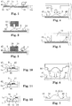
- Fig. 1 shows, in a cross-sectional view, a substrate 1 having at a first side a first surface 1a and at a second side a second surface 1b.
- Substrate 1 is a wafer, and only a small portion of the wafer is visible in Fig. 1 .
- a barrier member 40 is present which may describe a closed-loop shape such as a circle or a rectangle.
- a barrier member 40 describing a circular closed loop is illustrated in a top view.
- Substrate 1 defines lateral directions which are directions parallel to the first and second sides of substrate 1 and, accordingly, also vertical directions which are perpendicular to the lateral directions.
- An average level of first surface 1a is referred to as 1m.
- Barrier member 40 has a first partial surface 41 and a second partial surface 42 which are at an angle ⁇ amounting, in the example of Fig. 1 to about 320°. Partial surfaces 41, 42 may, as illustrated in Fig. 1 adjoin at an edge 45.
- second partial surface 42 may, in general for protruding barrier members 40, be vertically aligned, at least within ⁇ 35° or rather within ⁇ 15°.
- barrier member 40 may, in general for protruding barrier members 40, protrude beyond an average level described by the first surface by at least 2 ⁇ m or by at least 8 ⁇ m, and/or by at most 150 ⁇ m or by at most 80 ⁇ m.
- Fig. 2 illustrates substrate 1 of Fig. 1 in the same cross-sectional view, but during the process of applying an element 10 to substrate 1.
- a hardenable material 5 in a flowable state (typically a liquid hardenable material 5) has been brought into contact with surface 1a, such that on surface 1a, an amount of the material 5 is present.
- Hardenable material 5 may be, e.g., a heat-curable and/or a UV-curable adhesive, e.g., a heat-curable and/or a UV-curable epoxy resin.
- barrier member 40 present on substrate 1, element 10 is brought into contact with material 5, as illustrated by the open arrow in Fig. 2 .
- Fig. 3 the substrate of Figs. 1 and 2 is illustrated with element 10 attached to substrate 1 in its target position.
- Material 5 is hardened, such that element 10 is permanently fixed to substrate 1.
- barrier member 40 effects that a flow of material 5 (prior to the hardening) is controlled.
- material 5 shall not flow across barrier member 40.
- features or elements or any kind of items present beyond barrier member 40 are not exposed to and/or (partially) covered by some of the material 5. Accordingly, using barrier members can make possible to achieve a particularly high density of elements on a substrate.
- partial surface 41 of barrier member 40 is at least partially covered by material 5.
- region of surface 1a where element 10 is present at surface 1a is smooth, free of edges, and in addition, it is also planar, essentially flat.
- Element 10 may be virtually any kind of item to be attached to substrate 1, in particular a pre-fabricated item, e.g., an active optical component or a passive optical component, or an electronics component.
- Figs. 4 and 5 illustrate, similarly to Figs. 2 and 3 , respectively, the case that element 10 is a part of an extended substrate such as of a waferscale substrate, wherein on the waferscale substrate, elements may possibly be provided (pre-assembled elements). Element 10 may be a wafer or a portion of a wafer. Again, element 10 is in its target position (cf. Fig. 5 ) not before material 5 is applied to surface 1a.
- an element 10 to substrate 1 may also be accomplished in such a way that the element 10 is simultaneously (in one and the same process) created and applied (or attached) to surface 1a, e.g., as shown in Fig. 6 .
- Fig. 6 shows again the substrate of Fig. 1 during the process of applying an element 10, but element 10 comprises a replicated optical element to be created on surface 1a in an embossing-type process.
- a replication tool 50 is provided which determines at least in part the shape of element 10.
- Hardenable material 5 is more specifically a replication material, e.g., a curable epoxy resin. Material 5 is applied between replication tool 50 and substrate 1, e.g., as illustrated in Fig. 6 , applied to replication tool 50. Then, replication tool 50 is brought close to or even in contact with surface 1a, as illustrated by the open arrow.
- optical element 10 is a transparent optical element such as a lens
- material 5 is an optically transparent material
- substrate 1 may also be transparent, at least in part. Transparency may of course possibly refer to only a portion of the electromagnetic spectrum such as to infrared light only.
- hardenable material 5 is a replication material constituting element 10 in the example of Fig. 6 , it is merely an adhesive or bonding material in the examples of Figs. 2, 3 and 4, 5 .
- Fig. 7 shows substrate 1 of Fig. 6 with replication tool 50 removed and material 5 completely hardened.
- the element 10 is now created and present on (and solidly interconnected to) substrate 1 in its target position.
- elements may be produced which comprise, as illustrated in Fig. 7 , a main portion 11 constituting a functional element such as a lens element and, in addition, a surrounding portion 12 which completely (or at least in part) laterally surrounds the main portion 11.
- Main portion 11 and surrounding portion 12 are produced in one and the same process and of the same material. They constitute an integrally formed part (namely element 10).
- the surrounding portion 12 does not have a specific function, e.g., no optical function, but merely is a result of the way of manufacturing the main portion 11.
- such a surrounding portion may be used as a barrier member, as will be described referring to Fig. 8 .
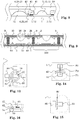
- Fig. 8 is a cross-sectional illustration of an application of an element 10 onto a substrate 1 by replicating the element 10 on substrate 1, wherein a barrier member 40 is provided by another element 20 previously replicated on the substrate 1.
- an element 20 has been produced on substrate 1 using an embossing-type process using a replication tool (not shown) and a flowable and/or liquid hardenable (replication) material 6.
- That element 20 comprises a main portion 21 and a surrounding portion 22.
- Surrounding portion 22 provides two partial surfaces 41, 42 which are at a large angle with each other and form an edge 45.
- the particular shape of surrounding portion 22 basically originates from a suitable design of the replication tool, which may, e.g., correspond to the design of the replication tool 50 of Fig. 6 .
- Partial surface 42 is a replication of a surface of the replication tool, whereas partial surface 42 has a meniscus shape which is determined by the amount of material 6 used in the replication process and by material properties, more particularly by the contact angle between material 6 and the material of the replication tool and also by the contact angle between material 6 and the material at surface 1a.
- Element 20 more particularly surrounding portion 22 and still more particularly partial surfaces 41, 42 (and edge 45) may, for a subsequent process, function as a barrier member 40.
- That subsequent process may be, e.g., again a replication process and more particularly an embossing process, as illustrated in Fig. 8.
- Fig. 8 illustrates the situation at the beginning of a hardening process for a (replication) material 5 applied to surface 1a which is formed by a replication tool 50.
- Material 5 (cf. the dotted lines in Fig. 8 ) is forced to flow as indicated by the black arrows. Its flow is controlled and stopped by barrier member 40 provided by surrounding portion 22 of the structure present on substrate 1 already in advance (cf. above).
- Material 5 constitutes a main portion 11 and a surrounding portion 12.
- two elements 10, 20 are present on substrate 1 which comprise, e.g., a lens element each and which are very close to each other. Their respective surrounding portions 12, 22 are (laterally) overlaping.
- Fig. 9 is an illustration of wafer-level manufactured devices which are opto-electronic modules 100, in a cross-sectional view before dicing.
- various elements have been applied to different substrates using barrier members for flow control.
- a hardenable material 5 (bonding material) has been used for connecting elements 10 such as image sensors to a substrate 1, and for connecting elements 30 such as replicated lens elements to a substrate 2, and for interconnecting substrates 1 and 2 via a spacer wafer representing an element 60.
- Substrate 2 comprises a non-transparent portion 2b through which light cannot pass and transparent portions 2t through which light can pass.
- a device such as a smart phone or a photographic device or another light sensing device or illumination device or still other optical device. Separation lines (dicing tracks) are referenced 9 in Fig. 9 .
- Fig. 10 is a cross-sectional illustration of a flow of material onto a barrier member 40 integrated in a substrate 1.
- Barrier member 40 has a shape similar to the one illustrated in Fig. 8 for the barrier member constituted by a surrounding portion of a replicated structure, having a concavely curved first partial surface 41.
- Fig. 10 symbolizes the surface of the hardenable material 5.
- the dark arrow indicates the direction of flow of material 5.
- partial surface 41 is covered by material 5.
- edge 45 is a particularly strong barrier to the flow of material 5.
- material 5 is controlled by barrier member 40, and material can be hardened, in particular in the state illustrated in Fig. 10 .
- Fig. 11 is an illustration of a flow of a hardenable material 5 onto a barrier member 40 dispensed onto a substrate 1.
- the illustration is similar to the one of Fig. 10 , however in this case, the substrate 1 is not pre-shaped (but is simply planar), and barrier member 40 has been added after manufacture of the (planar) substrate 1.
- a dispenser can be used for depositing material 5 on substrate 1, e.g., a dispenser like used for underfilling processes in electronics packaging.
- Fig. 16 is another cross-sectional illustration of a flow of material onto a barrier member 40, wherein the barrier member 40 is a structure protruding from substrate 1, more particularly the barrier member is provided by structured photoresist material. Otherwise, the illustration is similar to the one of Fig. 10 .
- Barrier member 40 has a first partial surface 41, a second partial surface 42, and a third partial surface 43. Partial surface 41 is interconnecting partial surfaces 42 and 43.
- a photoresist material is applied (on the first side of substrate 1), e.g., by spinning. This way, a photoresist film may be created. The film may cover one continuous region. Then, the photoresist material is structured, in particularly photolithographically structured, by locally illuminating it, e.g., with UV light, and subsequently removing the illuminated or the not illuminated part of the photoresist material. At least part of the remaining photoresist material then provides barrier members 40. Photoresist barrier members 40 may show an undercut, as illustrated in Fig. 16 . This way, a more efficient flow stopping at the edge between first partial surface 41 and second partial surface 42 is achieved. However, it is also possible that other flanks (not undercut flanks), e.g., straight flanks, are provided.
- the first partial surface 41 is usually horizontally aligned. Even though the flow of hardenable material 5 may stop already at the edge between third partial surface 43 and first partial surface 41, flow stopping is more effectively accomplished at the edge between intermediate partial surface 41 and second partial surface 42. Thus, usually, finally, third partial surface 43 and first partial surface 41 are both covered by hardenable material 5, while second partial surface 42 is free from hardenable material 5.
- Fig. 12 is yet another illustration similar to the ones of Figs. 10, 11 and 16 , but it is an illustration of a flow of material 5 towards a barrier member 40 which is a depression in a substrate 1.
- This substrate 1 may be either a pre-fabricated one in the sense that its shape (including the barrier members) is determined by its manufacture (e.g., by replication), in particular without additional steps for producing barrier members 40, or may be a substrate 1 obtained by manufacturing an initial substrate such as a planar substrate (cf. also Fig. 11 ), and then, material of the substrate is selectively removed in order to form barrier members 40.
- the subsequent removal of material may be accomplished, e.g., by using laser ablation, using selective etching (e.g., in lithographic methods), or by using a dicing saw.
- the flow control can be advantageous for the flow control to provide an edge 14 at that end of barrier 40 which is closest to the target position of the element to be applied to the substrate 1, i.e. at that end of barrier 40 which is closest the origin of flow of material 5.
- Said edge 14 may, in general for depressions, be present where the first partial surface adjoins the first surface of substrate 1.
- Having a particularly large angle between partial surface 41 and surface 1a (where it adjoins partial surface 41) can improve the flow control or flow-stop properties of barrier member 40.
- the angle is 270°.
- the first partial surface 41 may be vertically aligned, at least within ⁇ 35° or rather within ⁇ 15°.
- a barrier member may, in general for recessed barrier members (depressions), extend below an average level described by the first surface by at least 2 ⁇ m or by at least 8 ⁇ m, and/or by at most 150 ⁇ m or by at most 80 ⁇ m;
- Fig. 13 illustrates a top view of an element 10 and an associated barrier 40 member on a substrate 1.
- barrier member 40 may describe a loop completely laterally circumscribing element 10. This way, it can be prevented that any of the items 80 present on substrate 1 would be wetted or covered by material 5. And/or it can be prevented that place intended to be taken by items 80 would be covered or wetted by material 5. This might be useful, e.g., in case items 80 cannot be properly connected to substrate 1 if some of material is present in the intended location on substrate 1.
- the outer lateral boundary of material 5 is illustrated by the dotted line in Fig. 13 .
- Fig. 14 is a similar illustration as Fig. 13 .
- the barrier member 40 does not describe a closed-loop shape.
- An item 80 is located at substrate 1 in such a way that barrier member 40 is arranged laterally between it and the element 10 when applied to substrate 1.
- a thick solid straight line section illustrates points at the surface of substrate 1 which are prevented from being covered by material 5 by barrier member 40.
- An extension of the line passes through two points PI, P2, wherein PI is a central point of element 10 in the surface, more particularly a center of mass of the footprint of element 10 at the surface.
- point P2 designates a central point of barrier member 40 at the surface, more particularly a center of mass of the footprint of barrier member 40 at the surface.
- Fig. 15 is a similar illustration as Figs. 13 and 14 . In Fig. 15 , it is illustrated that a barrier member can also be discontinuous. Alternatively, Fig. 15 can also be interpreted to show several barrier members associated with element 10, and these barrier members protect item 80 from material 5.
- an element 10 is in its target position not before the material 5 gets into contact with the surface 1a of the substrate 1. Accordingly, the element is mounted on the surface 1a not before the material 5 gets into contact with the surface 1a. A process of mounting the element 10 on the substrate 1 is usually finished only after the hardenable material 5 is hardened (solidified).
- the substrate 1 In a lateral area where a barrier member is present at the substrate 1, the substrate 1 usually is thicker or thinner than its avergage thickness of substrate.
- a boundary of a footprint of an element 10 in the target position on surface 1a is (laterally) at a distance from the associated barrier member 40. And in particular, after the hardening of the material 5, the surface 1a is (typically completely) covered by the hardenable material 5 along said distance.
- a high density of (functional) elements on a substrate in wafer level manufacture can be achieved by means of the described methods. And specific ones of the elements can be positioned very close to each other, in particular without undesired overlap of material.
- contact angles described in the present patent application are, more precisely, “advancing contact angles” rather than “receding contact angles”, as is also clear from the described process.
Landscapes
- Engineering & Computer Science (AREA)
- Physics & Mathematics (AREA)
- General Physics & Mathematics (AREA)
- Microelectronics & Electronic Packaging (AREA)
- Power Engineering (AREA)
- Condensed Matter Physics & Semiconductors (AREA)
- Computer Hardware Design (AREA)
- Mechanical Engineering (AREA)
- Manufacturing & Machinery (AREA)
- Health & Medical Sciences (AREA)
- Dispersion Chemistry (AREA)
- Chemical & Material Sciences (AREA)
- Ophthalmology & Optometry (AREA)
- Optics & Photonics (AREA)
- Toxicology (AREA)
- Shaping Of Tube Ends By Bending Or Straightening (AREA)
- Casting Or Compression Moulding Of Plastics Or The Like (AREA)
- Micromachines (AREA)
- Led Device Packages (AREA)
- Mounting And Adjusting Of Optical Elements (AREA)
- Light Receiving Elements (AREA)
Claims (12)
- Wafer-Level-Verfahren zum Aufbringen von N ≥ 2 ersten Elementen (10) auf eine erste Seite eines Substrats (1), wobei das Substrat (1) an der ersten Seite eine erste Oberfläche (1a) bereitstellt, wobei das Verfahren umfassta) Bereitstellen des Substrats (1), wobei mindestens N Barriereelemente (40) auf der ersten Seite vorhanden sind und wobei jeder des N Barriereelemente (40) einem der N ersten Elemente (10) zugeordnet ist;
das Verfahren für jedes der N ersten Elemente (10) umfassendb) Inkontaktbringen einer jeweiligen ersten Menge eines aushärtbaren Materials (5) in einen fließfähigen Zustand mit der ersten Oberfläche (1a), wobei die jeweilige erste Menge an aushärtbarem Material (5) dem jeweiligen ersten Element (10) zugeordnet ist;c) Steuern eines Flusses der jeweiligen zugeordneten ersten Menge an aushärtbarem Material (5) auf der ersten Oberfläche (1a) mittels des jeweiligen zugeordneten Barriereelements (40);d) Härten der jeweiligen zugeordneten ersten Menge an aushärtbarem Material (5);wobei für jedes der N ersten Elemente (10) in Schritt d) eine Verbindung zwischen der ersten Oberfläche (1a) und dem jeweiligen ersten Element (10) hergestellt wird. - Verfahren nach Anspruch 1, wobei das Verfahren ein Wafer-Level-Verfahren zum Aufbringen der ersten N ≥ 2 ersten Elemente (10) auf die erste Seite eines Substrats (1) jeweils in einer jeweiligen Zielposition ist, und wobei für jedes der N ersten Elemente (10) gilt- während Schritt b) befindet sich das jeweilige erste Element (10) in einer Position, die sich von der jeweiligen Zielposition unterscheidet; und- in Schritt d) wird die Verbindung zwischen der ersten Oberfläche (la) und dem jeweiligen ersten Element (10) in der jeweiligen Zielposition hergestellt.
- Verfahren nach Anspruch 1 oder Anspruch 2, wobei ein Kontaktwinkel (θ) für das aushärtbare Material (5) auf dem Barriereelement (40) höchstens 90° und insbesondere höchstens 45° und noch genauer bis höchstens 30° beträgt.
- Verfahren nach einem der Ansprüche 1 bis 3, wobei das aushärtbare Material (5) durch Energieeintrag aushärtbar ist, wobei es insbesondere durch Erhitzen und/oder Bestrahlen mit elektromagnetischer Strahlung aushärtbar ist.
- Verfahren nach einem der Ansprüche 1 bis 4, wobei für jedes der N ersten Elemente (10) Schritt c) derart durchgeführt wird, dass am Ende von Schritt d) mindestens 60 %, insbesondere mindestens 80 % eines oberen Oberflächenbereichs des jeweiligen ersten Elements (10) frei von Material der jeweiligen ersten Menge an aushärtbarem Material (5) ist.
- Verfahren nach einem der Ansprüche 1 bis 5, wobei jedes der mindestens N Barriereelemente (40) eines von Folgendem ist oder durch eines oder mehrere von Folgendem bereitgestellt wird- eine replizierte Struktur, die an der ersten Oberfläche (1a) repliziert wird, bevor Schritt b) durchgeführt wird, wobei insbesondere die replizierte Struktur unter Verwendung eines prägungsartigen Prozesses repliziert wird, und wobei genauer gesagt die replizierte Struktur ein optisches Element (11) umfasst und zusätzlich einen umgebenden Abschnitt (12), der das optische Element (11) mindestens teilweise umgibt;- einen umgebenden Abschnitt (12) einer replizierten Struktur, die in der ersten Oberfläche (la) repliziert wird, bevor Schritt b) ausgeführt wird, wobei die replizierte Struktur zusätzlich zu dem umgebenden Abschnitt (12) ein Element, insbesondere ein optisches Element (11), umfasst, wobei der umgebende Abschnitt (12) das Element mindestens teilweise lateral umgibt, wobei insbesondere die replizierte Struktur unter Verwendung eines prägungsartigen Prozesses repliziert wird;- einen Vorsprung, der über ein durchschnittliches Niveau (1m) hinausragt, das von der ersten Oberfläche (1a) bezeichnet wird;- eine Vertiefung in der ersten Seite des Substrats (1), die sich unterhalb eines Durchschnittsniveaus (1m) erstreckt, das von der ersten Oberfläche (la) bezeichnet wird;- eine Struktur, die auf der ersten Oberfläche (la) unter Verwendung eines Replikationsverfahrens, insbesondere eines prägungsartigen Prozesses, gebildet wird;- eine Struktur, die auf der ersten Oberfläche (la) unter Verwendung eines Verteilverfahrens, insbesondere unter Verwendung einer Verteileinrichtung, gebildet wird;- einen Gegenstand, der an die erste Oberfläche (la) gebunden ist, insbesondere einen vorgefertigten Gegenstand, der an die erste Oberfläche (1a) gebunden ist, insbesondere unter Verwendung eines Bindematerials an die erste Oberfläche (1a) gebunden ist;- eine Struktur, die an der ersten Oberfläche (la) durch Entfernen von Material von dem Substrat (1) gebildet wird, insbesondere unter Verwendung eines Laserstrahls zum Entfernen von Material von dem Substrat (1), insbesondere einer Laserablation;- eine Struktur, die an der ersten Oberfläche (la) unter Verwendung eines photolithographischen Verfahrens mit einem Ätzschritt oder Abhebungsschritt gebildet wird, insbesondere unter Verwendung eines Laser-Lithographie-Verfahrens;- eine Struktur, die an der ersten Oberfläche (la) durch Bearbeiten, insbesondere Fräsen, z. B. mit einer Fräsmaschine, gebildet wird;- eine Struktur, die an der ersten Oberfläche (la) unter Verwendung einer Säge, insbesondere einer Trennsäge, gebildet wird;- ein Strukturmerkmal an dem ersten Substrat (1), das einstückig mit dem mindestens einen überwiegenden Teil des restlichen Substrats (1) gebildet wird, wobei insbesondere das Substrat (1) unter Verwendung eines Replikationsverfahrens, insbesondere eines prägungsartigen oder gussartigen Replikationsverfahrens, hergestellt wird.
- Verfahren nach einem der Ansprüche 1 bis 6, wobei jedes der N ersten Elemente (10) eines oder mehrere von Folgendem ist oder umfasst- eine replizierte Struktur, die an der ersten Oberfläche (1a) repliziert wird, umfassend die Schritte b), c) und d), wobei insbesondere die replizierte Struktur unter Verwendung eines prägungsartigen Prozesses repliziert wird, und wobei genauer gesagt die replizierte Struktur ein optisches Element (11) und zusätzlich einen umgebenden Abschnitt (12), der das optische Element (11) mindestens teilweise umgibt, umfasst;- einen Gegenstand, der an die erste Oberfläche (la) zu binden ist, insbesondere ein vorgefertigter Gegenstand, der an die erste Oberfläche (1a) zu binden ist, der insbesondere mit der ersten Oberfläche (la) unter Verwendung eines Bindematerials, z. B. einer vorgefertigten optischen Massenkomponente, gebunden ist;- eine mikrooptische Komponente, insbesondere eine transparente mikrooptische Komponente;- eine passive optische Komponente, insbesondere ein Linsenelement;- eine aktive optische Komponente;- eine elektronische Komponente;- ein lichtemittierendes Element, insbesondere eine LED, eine OLED, eine Laserdiode;- ein Lichterfassungselement, insbesondere eine Fotodiode oder ein Lichtdetektorarray;- eine mikromechanische Komponente;- eine mikrofluidische Komponente;- einen Abschnitt eines Wafers, insbesondere mindestens ein Kontaktabstandshalter eines Abstandswafers.
- Verfahren nach einem der Ansprüche 1 bis 7, wobei das Verfahren für jedes der N ersten Elemente (10) umfasstr) Herstellen des ersten Elements (10) an der ersten Oberfläche (1a) mittels eines prägungsartigen Replikationsverfahrens;wobei Schritt r) umfasstr1) Verwenden eines Replikationswerkzeugs (50) zum Formen mindestens eines Teils der ersten Menge an aushärtbarem Material (5);r2) Entfernen des Replikationswerkzeugs (50) von der ersten Menge an aushärtbarem Material (5) während oder nach Schritt h).
- Verfahren nach einem der Ansprüche 1 bis 8, wobei jedes der N Barriereelemente (40) einen Vorsprung umfasst, der über ein Durchschnittsniveau (1m) hinausragt, das durch die erste Oberfläche (la) bezeichnet wird, wobei der jeweilige Vorsprung eine erste Teiloberfläche (41) umfasst, die dem jeweiligen ersten Element (10) in ihrer Position am Ende von Schritt d) zugewandt ist und/oder horizontal innerhalb von ±35° ausgerichtet ist, und eine zweite Teilfläche (42), die vom jeweiligen ersten Element (10) in ihrer Position am Ende von Schritt d) weg weist, wobei die erste Teilfläche (41) am Ende von Schritt d) mindestens teilweise von aushärtbarem Material (5) der jeweils zugeordneten ersten Menge an aushärtbarem Material (5) bedeckt ist, und wobei die zweite Teilfläche (4) am Ende von Schritt d) frei von aushärtbarem Material (5) der jeweiligen zugeordneten ersten Menge an aushärtbarem Material (5) ist, wobei insbesondere die erste und die zweite Teilfläche (42) an einer Kante aneinandergrenzen und die erste Teilfläche (41) am Ende von Schritt d) von aushärtbarem Material (5) der jeweiligen zugeordneten ersten Menge an aushärtbarem Material (5) bis zum Rand bedeckt (42) ist.
- Verfahren nach einem der Ansprüche 1 bis 8, wobei jedes der N Barriereelemente (40) eine Vertiefung an der ersten Seite des Substrats (1) umfasst, die sich unterhalb eines Durchschnittsniveaus erstreckt, das durch die erste Oberfläche (la) bezeichnet wird, wobei die jeweilige Vertiefung eine erste Teilfläche (41) umfasst, die dem jeweiligen ersten Element (10) in ihrer Position am Ende von Schritt d) weg weist, und eine zweite Teilfläche (42), wobei die erste Teilfläche (41) am Ende von Schritt d) frei von aushärtbarem Material (5) der jeweiligen zugeordneten ersten Menge an aushärtbarem Material (5) ist oder höchstens teilweise von diesem bedeckt ist, und wobei die zweite Teilfläche (42) am Ende von Schritt d) frei von aushärtbarem Material (5) der jeweiligen zugeordneten ersten Menge an aushärtbarem Material (5) ist, wobei insbesondere die erste Teilfläche (41) eine Begrenzung aufweist, an der eine Kante (45) vorhanden ist, wobei am Ende von Schritt d) sich das Material der ersten Menge an aushärtbarem Material (5) bis zu der Kante (45) erstreckt, aber die erste Teilfläche (41) frei von aushärtbarem Material (5) der jeweiligen zugeordneten ersten Menge an aushärtbarem Material (5) ist, wobei insbesondere vorgesehen sein kann, dass die zweite Teilfläche (42) innerhalb von ±35° horizontal ausgerichtet ist und/oder dem jeweiligen ersten Element (10) in ihrer Position am Ende von Schritt d) zugewandt ist.
- Verfahren nach einem der Ansprüche 1 bis 10, wobei jedes der N Barriereelemente (40) mindestens eines von Folgendem bildet- einen Vorsprung, der über ein Durchschnittsniveau, das durch die erste Oberfläche (la) bezeichnet wird, um mindestens 2 µm und/oder um höchstens 150 µm, insbesondere um zwischen 4 µm und 100 µm, vorsteht; und- eine Vertiefung in der ersten Seite des Substrats (1), die sich unterhalb eines Durchschnittsniveaus, das durch die erste Oberfläche (1a) bezeichnet wird, um mindestens 2 µm und/oder um höchstens 150 µm, insbesondere um zwischen 4 µm und 100 µm, erstreckt.
- Verfahren zum Herstellen einer Vorrichtung, umfassend einen Abschnitt eines Substrats (1), auf dem ein bestimmtes erstes Element (10) vorhanden ist, wobei das Verfahren das Aufbringen von N ≥ 2 ersten Elementen (10) nach einem der Ansprüche 1 bis 11 auf eine erste Seite des Substrats (1) umfasst, wobei die N ≥ 2 ersten Elemente (10) das spezifische erste Element (10) umfassen und das Substrat (1) den Substratabschnitt umfasst.
Applications Claiming Priority (2)
| Application Number | Priority Date | Filing Date | Title |
|---|---|---|---|
| US201461994358P | 2014-05-16 | 2014-05-16 | |
| PCT/SG2015/050113 WO2015174930A1 (en) | 2014-05-16 | 2015-05-14 | Wafer-level maufacture of devices, in particular of optical devices |
Publications (3)
| Publication Number | Publication Date |
|---|---|
| EP3142859A1 EP3142859A1 (de) | 2017-03-22 |
| EP3142859A4 EP3142859A4 (de) | 2018-01-24 |
| EP3142859B1 true EP3142859B1 (de) | 2019-07-10 |
Family
ID=54480324
Family Applications (1)
| Application Number | Title | Priority Date | Filing Date |
|---|---|---|---|
| EP15793119.7A Active EP3142859B1 (de) | 2014-05-16 | 2015-05-14 | Herstellung von vorrichtungen, insbesondere von optischen vorrichtungen, auf wafer-ebene |
Country Status (8)
| Country | Link |
|---|---|
| US (1) | US10682824B2 (de) |
| EP (1) | EP3142859B1 (de) |
| JP (2) | JP2017526977A (de) |
| KR (1) | KR102352424B1 (de) |
| CN (1) | CN106573460B (de) |
| SG (2) | SG11201609001TA (de) |
| TW (1) | TWI710455B (de) |
| WO (1) | WO2015174930A1 (de) |
Families Citing this family (7)
| Publication number | Priority date | Publication date | Assignee | Title |
|---|---|---|---|---|
| NL2016689B1 (en) * | 2016-04-28 | 2017-11-20 | Anteryon Wafer Optics B V | Replication tool |
| CN109116680A (zh) * | 2018-09-27 | 2019-01-01 | 京东方科技集团股份有限公司 | 压印模板及其制作方法 |
| US10867955B2 (en) * | 2018-09-27 | 2020-12-15 | Taiwan Semiconductor Manufacturing Company, Ltd. | Package structure having adhesive layer surrounded dam structure |
| CN113557122A (zh) * | 2019-03-12 | 2021-10-26 | ams传感器新加坡私人有限公司 | 庭院控制特征 |
| WO2020242378A1 (en) * | 2019-05-30 | 2020-12-03 | Ams Sensors Singapore Pte. Ltd. | Method of replicating optical elements and replicated optical elements |
| GB2594998A (en) * | 2020-05-15 | 2021-11-17 | Ams Sensors Asia Pte Ltd | Wafer level chip scale packaging |
| CN115097553B (zh) * | 2022-06-24 | 2023-10-31 | 京东方科技集团股份有限公司 | 微透镜阵列基板及其制备方法、显示装置 |
Family Cites Families (18)
| Publication number | Priority date | Publication date | Assignee | Title |
|---|---|---|---|---|
| JP4963148B2 (ja) * | 2001-09-18 | 2012-06-27 | ルネサスエレクトロニクス株式会社 | 半導体装置の製造方法 |
| TW544894B (en) | 2002-04-10 | 2003-08-01 | Siliconware Precision Industries Co Ltd | Chip carrier with dam bar |
| EP1443344A1 (de) * | 2003-01-29 | 2004-08-04 | Heptagon Oy | Herstellung von mikrostrukturierten Teilen |
| US20040241323A1 (en) | 2003-05-29 | 2004-12-02 | 3M Innovative Properties Company | Method for applying adhesive to a substrate |
| JP4362380B2 (ja) * | 2004-01-13 | 2009-11-11 | フジノン株式会社 | 光学素子の成形方法及び組み合わせ光学素子 |
| US20070216048A1 (en) | 2006-03-20 | 2007-09-20 | Heptagon Oy | Manufacturing optical elements |
| US20070216046A1 (en) | 2006-03-20 | 2007-09-20 | Heptagon Oy | Manufacturing miniature structured elements with tool incorporating spacer elements |
| US20080113160A1 (en) | 2006-11-14 | 2008-05-15 | Glimmerglass Networks, Inc. | Method And Apparatus For Localized Bonding |
| JP4507126B2 (ja) * | 2007-10-29 | 2010-07-21 | ソニー株式会社 | 偏光板の製造方法 |
| US20090159200A1 (en) | 2007-12-19 | 2009-06-25 | Heptagon Oy | Spacer element and method for manufacturing a spacer element |
| JP2009204752A (ja) | 2008-02-26 | 2009-09-10 | Sanyo Electric Co Ltd | 複合レンズ |
| JP2010052086A (ja) | 2008-08-28 | 2010-03-11 | Oki Semiconductor Co Ltd | 半導体装置及びその製造方法 |
| JP5047243B2 (ja) * | 2008-09-26 | 2012-10-10 | シャープ株式会社 | 光学素子ウエハモジュール、光学素子モジュール、光学素子モジュールの製造方法、電子素子ウエハモジュール、電子素子モジュールの製造方法、電子素子モジュールおよび電子情報機器 |
| WO2010143466A1 (ja) | 2009-06-12 | 2010-12-16 | コニカミノルタオプト株式会社 | ウエハレンズの製造方法、中間型、光学部品、成形型及び成形型の製造方法 |
| US20130273238A1 (en) * | 2012-04-16 | 2013-10-17 | Peter S. Andrews | Inverted Curing of Liquid Optoelectronic Lenses |
| WO2013179765A1 (ja) | 2012-05-30 | 2013-12-05 | オリンパス株式会社 | 撮像装置の製造方法および半導体装置の製造方法 |
| CN107490815B (zh) | 2012-09-11 | 2020-03-17 | 新加坡恒立私人有限公司 | 截断型镜片、截断型镜片对及相应装置的制造 |
| CN104854483A (zh) | 2012-12-15 | 2015-08-19 | 柯尼卡美能达株式会社 | 透镜阵列构造体的制造方法以及透镜阵列构造体 |
-
2015
- 2015-05-14 CN CN201580025271.5A patent/CN106573460B/zh active Active
- 2015-05-14 SG SG11201609001TA patent/SG11201609001TA/en unknown
- 2015-05-14 US US15/310,838 patent/US10682824B2/en active Active
- 2015-05-14 EP EP15793119.7A patent/EP3142859B1/de active Active
- 2015-05-14 KR KR1020167035043A patent/KR102352424B1/ko active IP Right Grant
- 2015-05-14 JP JP2017512630A patent/JP2017526977A/ja active Pending
- 2015-05-14 WO PCT/SG2015/050113 patent/WO2015174930A1/en active Application Filing
- 2015-05-14 TW TW104115387A patent/TWI710455B/zh active
- 2015-05-14 SG SG10201810219TA patent/SG10201810219TA/en unknown
-
2020
- 2020-02-26 JP JP2020030681A patent/JP6987907B2/ja active Active
Non-Patent Citations (1)
| Title |
|---|
| None * |
Also Published As
| Publication number | Publication date |
|---|---|
| KR20170029422A (ko) | 2017-03-15 |
| TW201605608A (zh) | 2016-02-16 |
| EP3142859A1 (de) | 2017-03-22 |
| US10682824B2 (en) | 2020-06-16 |
| CN106573460B (zh) | 2019-11-29 |
| TWI710455B (zh) | 2020-11-21 |
| SG11201609001TA (en) | 2016-11-29 |
| CN106573460A (zh) | 2017-04-19 |
| JP2017526977A (ja) | 2017-09-14 |
| EP3142859A4 (de) | 2018-01-24 |
| WO2015174930A1 (en) | 2015-11-19 |
| SG10201810219TA (en) | 2018-12-28 |
| KR102352424B1 (ko) | 2022-01-17 |
| JP2020106856A (ja) | 2020-07-09 |
| JP6987907B2 (ja) | 2022-01-05 |
| US20170087784A1 (en) | 2017-03-30 |
Similar Documents
| Publication | Publication Date | Title |
|---|---|---|
| EP3142859B1 (de) | Herstellung von vorrichtungen, insbesondere von optischen vorrichtungen, auf wafer-ebene | |
| US7457490B2 (en) | Micro-optics on optoelectronics | |
| EP2225596B1 (de) | Distanzstück und herstellungsverfahren für ein distanzstück | |
| EP3378096B1 (de) | Dünne optoelektronische module mit öffnungen und deren herstellung | |
| EP2735029B1 (de) | Verfahren zur herstellung passiver optischer komponenten und vorrichtungen damit | |
| US8294229B2 (en) | Wafer-scale array of optical packages and method for fabricating the same | |
| US10126530B2 (en) | Fabrication of optical elements and modules incorporating the same | |
| KR101445022B1 (ko) | 멀티-레이어 폴리머 렌즈, 렌즈 형성 방법 및 렌즈 어셈블리 | |
| CN107490815B (zh) | 截断型镜片、截断型镜片对及相应装置的制造 | |
| NL2015330B1 (en) | A method of fabricating an array of optical lens elements | |
| EP3341974B1 (de) | Optische anordnungen mit einem direkt an einem substrat haftenden abstandhalter |
Legal Events
| Date | Code | Title | Description |
|---|---|---|---|
| STAA | Information on the status of an ep patent application or granted ep patent |
Free format text: STATUS: THE INTERNATIONAL PUBLICATION HAS BEEN MADE |
|
| PUAI | Public reference made under article 153(3) epc to a published international application that has entered the european phase |
Free format text: ORIGINAL CODE: 0009012 |
|
| STAA | Information on the status of an ep patent application or granted ep patent |
Free format text: STATUS: REQUEST FOR EXAMINATION WAS MADE |
|
| 17P | Request for examination filed |
Effective date: 20161031 |
|
| AK | Designated contracting states |
Kind code of ref document: A1 Designated state(s): AL AT BE BG CH CY CZ DE DK EE ES FI FR GB GR HR HU IE IS IT LI LT LU LV MC MK MT NL NO PL PT RO RS SE SI SK SM TR |
|
| AX | Request for extension of the european patent |
Extension state: BA ME |
|
| DAV | Request for validation of the european patent (deleted) | ||
| DAX | Request for extension of the european patent (deleted) | ||
| A4 | Supplementary search report drawn up and despatched |
Effective date: 20171221 |
|
| RIC1 | Information provided on ipc code assigned before grant |
Ipc: B32B 37/12 20060101ALI20171215BHEP Ipc: H01L 23/28 20060101ALI20171215BHEP Ipc: B32B 41/00 20060101AFI20171215BHEP |
|
| RIC1 | Information provided on ipc code assigned before grant |
Ipc: B32B 41/00 20060101AFI20181102BHEP Ipc: B32B 37/12 20060101ALI20181102BHEP Ipc: H01L 23/28 20060101ALI20181102BHEP |
|
| GRAP | Despatch of communication of intention to grant a patent |
Free format text: ORIGINAL CODE: EPIDOSNIGR1 |
|
| STAA | Information on the status of an ep patent application or granted ep patent |
Free format text: STATUS: GRANT OF PATENT IS INTENDED |
|
| INTG | Intention to grant announced |
Effective date: 20181214 |
|
| GRAS | Grant fee paid |
Free format text: ORIGINAL CODE: EPIDOSNIGR3 |
|
| GRAA | (expected) grant |
Free format text: ORIGINAL CODE: 0009210 |
|
| STAA | Information on the status of an ep patent application or granted ep patent |
Free format text: STATUS: THE PATENT HAS BEEN GRANTED |
|
| AK | Designated contracting states |
Kind code of ref document: B1 Designated state(s): AL AT BE BG CH CY CZ DE DK EE ES FI FR GB GR HR HU IE IS IT LI LT LU LV MC MK MT NL NO PL PT RO RS SE SI SK SM TR |
|
| REG | Reference to a national code |
Ref country code: GB Ref legal event code: FG4D |
|
| REG | Reference to a national code |
Ref country code: CH Ref legal event code: EP Ref country code: AT Ref legal event code: REF Ref document number: 1153086 Country of ref document: AT Kind code of ref document: T Effective date: 20190715 |
|
| REG | Reference to a national code |
Ref country code: DE Ref legal event code: R096 Ref document number: 602015033617 Country of ref document: DE |
|
| REG | Reference to a national code |
Ref country code: IE Ref legal event code: FG4D |
|
| REG | Reference to a national code |
Ref country code: NL Ref legal event code: MP Effective date: 20190710 |
|
| REG | Reference to a national code |
Ref country code: LT Ref legal event code: MG4D |
|
| REG | Reference to a national code |
Ref country code: AT Ref legal event code: MK05 Ref document number: 1153086 Country of ref document: AT Kind code of ref document: T Effective date: 20190710 |
|
| PG25 | Lapsed in a contracting state [announced via postgrant information from national office to epo] |
Ref country code: HR Free format text: LAPSE BECAUSE OF FAILURE TO SUBMIT A TRANSLATION OF THE DESCRIPTION OR TO PAY THE FEE WITHIN THE PRESCRIBED TIME-LIMIT Effective date: 20190710 Ref country code: PT Free format text: LAPSE BECAUSE OF FAILURE TO SUBMIT A TRANSLATION OF THE DESCRIPTION OR TO PAY THE FEE WITHIN THE PRESCRIBED TIME-LIMIT Effective date: 20191111 Ref country code: SE Free format text: LAPSE BECAUSE OF FAILURE TO SUBMIT A TRANSLATION OF THE DESCRIPTION OR TO PAY THE FEE WITHIN THE PRESCRIBED TIME-LIMIT Effective date: 20190710 Ref country code: AT Free format text: LAPSE BECAUSE OF FAILURE TO SUBMIT A TRANSLATION OF THE DESCRIPTION OR TO PAY THE FEE WITHIN THE PRESCRIBED TIME-LIMIT Effective date: 20190710 Ref country code: NO Free format text: LAPSE BECAUSE OF FAILURE TO SUBMIT A TRANSLATION OF THE DESCRIPTION OR TO PAY THE FEE WITHIN THE PRESCRIBED TIME-LIMIT Effective date: 20191010 Ref country code: FI Free format text: LAPSE BECAUSE OF FAILURE TO SUBMIT A TRANSLATION OF THE DESCRIPTION OR TO PAY THE FEE WITHIN THE PRESCRIBED TIME-LIMIT Effective date: 20190710 Ref country code: BG Free format text: LAPSE BECAUSE OF FAILURE TO SUBMIT A TRANSLATION OF THE DESCRIPTION OR TO PAY THE FEE WITHIN THE PRESCRIBED TIME-LIMIT Effective date: 20191010 Ref country code: NL Free format text: LAPSE BECAUSE OF FAILURE TO SUBMIT A TRANSLATION OF THE DESCRIPTION OR TO PAY THE FEE WITHIN THE PRESCRIBED TIME-LIMIT Effective date: 20190710 Ref country code: LT Free format text: LAPSE BECAUSE OF FAILURE TO SUBMIT A TRANSLATION OF THE DESCRIPTION OR TO PAY THE FEE WITHIN THE PRESCRIBED TIME-LIMIT Effective date: 20190710 |
|
| PG25 | Lapsed in a contracting state [announced via postgrant information from national office to epo] |
Ref country code: RS Free format text: LAPSE BECAUSE OF FAILURE TO SUBMIT A TRANSLATION OF THE DESCRIPTION OR TO PAY THE FEE WITHIN THE PRESCRIBED TIME-LIMIT Effective date: 20190710 Ref country code: IS Free format text: LAPSE BECAUSE OF FAILURE TO SUBMIT A TRANSLATION OF THE DESCRIPTION OR TO PAY THE FEE WITHIN THE PRESCRIBED TIME-LIMIT Effective date: 20191110 Ref country code: GR Free format text: LAPSE BECAUSE OF FAILURE TO SUBMIT A TRANSLATION OF THE DESCRIPTION OR TO PAY THE FEE WITHIN THE PRESCRIBED TIME-LIMIT Effective date: 20191011 Ref country code: LV Free format text: LAPSE BECAUSE OF FAILURE TO SUBMIT A TRANSLATION OF THE DESCRIPTION OR TO PAY THE FEE WITHIN THE PRESCRIBED TIME-LIMIT Effective date: 20190710 Ref country code: AL Free format text: LAPSE BECAUSE OF FAILURE TO SUBMIT A TRANSLATION OF THE DESCRIPTION OR TO PAY THE FEE WITHIN THE PRESCRIBED TIME-LIMIT Effective date: 20190710 Ref country code: ES Free format text: LAPSE BECAUSE OF FAILURE TO SUBMIT A TRANSLATION OF THE DESCRIPTION OR TO PAY THE FEE WITHIN THE PRESCRIBED TIME-LIMIT Effective date: 20190710 |
|
| PG25 | Lapsed in a contracting state [announced via postgrant information from national office to epo] |
Ref country code: TR Free format text: LAPSE BECAUSE OF FAILURE TO SUBMIT A TRANSLATION OF THE DESCRIPTION OR TO PAY THE FEE WITHIN THE PRESCRIBED TIME-LIMIT Effective date: 20190710 |
|
| PG25 | Lapsed in a contracting state [announced via postgrant information from national office to epo] |
Ref country code: RO Free format text: LAPSE BECAUSE OF FAILURE TO SUBMIT A TRANSLATION OF THE DESCRIPTION OR TO PAY THE FEE WITHIN THE PRESCRIBED TIME-LIMIT Effective date: 20190710 Ref country code: IT Free format text: LAPSE BECAUSE OF FAILURE TO SUBMIT A TRANSLATION OF THE DESCRIPTION OR TO PAY THE FEE WITHIN THE PRESCRIBED TIME-LIMIT Effective date: 20190710 Ref country code: EE Free format text: LAPSE BECAUSE OF FAILURE TO SUBMIT A TRANSLATION OF THE DESCRIPTION OR TO PAY THE FEE WITHIN THE PRESCRIBED TIME-LIMIT Effective date: 20190710 Ref country code: DK Free format text: LAPSE BECAUSE OF FAILURE TO SUBMIT A TRANSLATION OF THE DESCRIPTION OR TO PAY THE FEE WITHIN THE PRESCRIBED TIME-LIMIT Effective date: 20190710 Ref country code: PL Free format text: LAPSE BECAUSE OF FAILURE TO SUBMIT A TRANSLATION OF THE DESCRIPTION OR TO PAY THE FEE WITHIN THE PRESCRIBED TIME-LIMIT Effective date: 20190710 |
|
| PG25 | Lapsed in a contracting state [announced via postgrant information from national office to epo] |
Ref country code: SM Free format text: LAPSE BECAUSE OF FAILURE TO SUBMIT A TRANSLATION OF THE DESCRIPTION OR TO PAY THE FEE WITHIN THE PRESCRIBED TIME-LIMIT Effective date: 20190710 Ref country code: IS Free format text: LAPSE BECAUSE OF FAILURE TO SUBMIT A TRANSLATION OF THE DESCRIPTION OR TO PAY THE FEE WITHIN THE PRESCRIBED TIME-LIMIT Effective date: 20200224 Ref country code: CZ Free format text: LAPSE BECAUSE OF FAILURE TO SUBMIT A TRANSLATION OF THE DESCRIPTION OR TO PAY THE FEE WITHIN THE PRESCRIBED TIME-LIMIT Effective date: 20190710 Ref country code: SK Free format text: LAPSE BECAUSE OF FAILURE TO SUBMIT A TRANSLATION OF THE DESCRIPTION OR TO PAY THE FEE WITHIN THE PRESCRIBED TIME-LIMIT Effective date: 20190710 |
|
| REG | Reference to a national code |
Ref country code: DE Ref legal event code: R097 Ref document number: 602015033617 Country of ref document: DE |
|
| PLBE | No opposition filed within time limit |
Free format text: ORIGINAL CODE: 0009261 |
|
| STAA | Information on the status of an ep patent application or granted ep patent |
Free format text: STATUS: NO OPPOSITION FILED WITHIN TIME LIMIT |
|
| PG2D | Information on lapse in contracting state deleted |
Ref country code: IS |
|
| 26N | No opposition filed |
Effective date: 20200603 |
|
| PG25 | Lapsed in a contracting state [announced via postgrant information from national office to epo] |
Ref country code: SI Free format text: LAPSE BECAUSE OF FAILURE TO SUBMIT A TRANSLATION OF THE DESCRIPTION OR TO PAY THE FEE WITHIN THE PRESCRIBED TIME-LIMIT Effective date: 20190710 |
|
| PG25 | Lapsed in a contracting state [announced via postgrant information from national office to epo] |
Ref country code: LI Free format text: LAPSE BECAUSE OF NON-PAYMENT OF DUE FEES Effective date: 20200531 Ref country code: CH Free format text: LAPSE BECAUSE OF NON-PAYMENT OF DUE FEES Effective date: 20200531 Ref country code: MC Free format text: LAPSE BECAUSE OF FAILURE TO SUBMIT A TRANSLATION OF THE DESCRIPTION OR TO PAY THE FEE WITHIN THE PRESCRIBED TIME-LIMIT Effective date: 20190710 |
|
| REG | Reference to a national code |
Ref country code: BE Ref legal event code: MM Effective date: 20200531 |
|
| PG25 | Lapsed in a contracting state [announced via postgrant information from national office to epo] |
Ref country code: LU Free format text: LAPSE BECAUSE OF NON-PAYMENT OF DUE FEES Effective date: 20200514 |
|
| PG25 | Lapsed in a contracting state [announced via postgrant information from national office to epo] |
Ref country code: IE Free format text: LAPSE BECAUSE OF NON-PAYMENT OF DUE FEES Effective date: 20200514 |
|
| PG25 | Lapsed in a contracting state [announced via postgrant information from national office to epo] |
Ref country code: BE Free format text: LAPSE BECAUSE OF NON-PAYMENT OF DUE FEES Effective date: 20200531 |
|
| PG25 | Lapsed in a contracting state [announced via postgrant information from national office to epo] |
Ref country code: MT Free format text: LAPSE BECAUSE OF FAILURE TO SUBMIT A TRANSLATION OF THE DESCRIPTION OR TO PAY THE FEE WITHIN THE PRESCRIBED TIME-LIMIT Effective date: 20190710 Ref country code: CY Free format text: LAPSE BECAUSE OF FAILURE TO SUBMIT A TRANSLATION OF THE DESCRIPTION OR TO PAY THE FEE WITHIN THE PRESCRIBED TIME-LIMIT Effective date: 20190710 |
|
| PG25 | Lapsed in a contracting state [announced via postgrant information from national office to epo] |
Ref country code: MK Free format text: LAPSE BECAUSE OF FAILURE TO SUBMIT A TRANSLATION OF THE DESCRIPTION OR TO PAY THE FEE WITHIN THE PRESCRIBED TIME-LIMIT Effective date: 20190710 |
|
| PGFP | Annual fee paid to national office [announced via postgrant information from national office to epo] |
Ref country code: DE Payment date: 20230519 Year of fee payment: 9 |
|
| P01 | Opt-out of the competence of the unified patent court (upc) registered |
Effective date: 20230825 |
|
| REG | Reference to a national code |
Ref country code: DE Ref legal event code: R082 Ref document number: 602015033617 Country of ref document: DE Representative=s name: VIERING, JENTSCHURA & PARTNER MBB PATENT- UND , DE |
|
| PGFP | Annual fee paid to national office [announced via postgrant information from national office to epo] |
Ref country code: GB Payment date: 20240521 Year of fee payment: 10 |
|
| PGFP | Annual fee paid to national office [announced via postgrant information from national office to epo] |
Ref country code: FR Payment date: 20240528 Year of fee payment: 10 |