EP3142145A1 - Method of forming integrated circuit contacts - Google Patents
Method of forming integrated circuit contacts Download PDFInfo
- Publication number
- EP3142145A1 EP3142145A1 EP16191250.6A EP16191250A EP3142145A1 EP 3142145 A1 EP3142145 A1 EP 3142145A1 EP 16191250 A EP16191250 A EP 16191250A EP 3142145 A1 EP3142145 A1 EP 3142145A1
- Authority
- EP
- European Patent Office
- Prior art keywords
- dielectric layer
- layer
- forming
- regions
- conductive
- Prior art date
- Legal status (The legal status is an assumption and is not a legal conclusion. Google has not performed a legal analysis and makes no representation as to the accuracy of the status listed.)
- Granted
Links
Images




Classifications
-
- H—ELECTRICITY
- H10—SEMICONDUCTOR DEVICES; ELECTRIC SOLID-STATE DEVICES NOT OTHERWISE PROVIDED FOR
- H10W—GENERIC PACKAGES, INTERCONNECTIONS, CONNECTORS OR OTHER CONSTRUCTIONAL DETAILS OF DEVICES COVERED BY CLASS H10
- H10W20/00—Interconnections in chips, wafers or substrates
- H10W20/01—Manufacture or treatment
- H10W20/071—Manufacture or treatment of dielectric parts thereof
- H10W20/074—Manufacture or treatment of dielectric parts thereof of dielectric parts comprising thin functional dielectric layers, e.g. dielectric etch-stop, barrier, capping or liner layers
- H10W20/075—Manufacture or treatment of dielectric parts thereof of dielectric parts comprising thin functional dielectric layers, e.g. dielectric etch-stop, barrier, capping or liner layers of multilayered thin functional dielectric layers
-
- H—ELECTRICITY
- H10—SEMICONDUCTOR DEVICES; ELECTRIC SOLID-STATE DEVICES NOT OTHERWISE PROVIDED FOR
- H10W—GENERIC PACKAGES, INTERCONNECTIONS, CONNECTORS OR OTHER CONSTRUCTIONAL DETAILS OF DEVICES COVERED BY CLASS H10
- H10W20/00—Interconnections in chips, wafers or substrates
- H10W20/01—Manufacture or treatment
- H10W20/071—Manufacture or treatment of dielectric parts thereof
- H10W20/074—Manufacture or treatment of dielectric parts thereof of dielectric parts comprising thin functional dielectric layers, e.g. dielectric etch-stop, barrier, capping or liner layers
- H10W20/077—Manufacture or treatment of dielectric parts thereof of dielectric parts comprising thin functional dielectric layers, e.g. dielectric etch-stop, barrier, capping or liner layers on sidewalls or on top surfaces of conductors
-
- H—ELECTRICITY
- H10—SEMICONDUCTOR DEVICES; ELECTRIC SOLID-STATE DEVICES NOT OTHERWISE PROVIDED FOR
- H10W—GENERIC PACKAGES, INTERCONNECTIONS, CONNECTORS OR OTHER CONSTRUCTIONAL DETAILS OF DEVICES COVERED BY CLASS H10
- H10W20/00—Interconnections in chips, wafers or substrates
- H10W20/01—Manufacture or treatment
- H10W20/071—Manufacture or treatment of dielectric parts thereof
- H10W20/081—Manufacture or treatment of dielectric parts thereof by forming openings in the dielectric parts
- H10W20/089—Manufacture or treatment of dielectric parts thereof by forming openings in the dielectric parts using processes for implementing desired shapes or dispositions of the openings, e.g. double patterning
-
- H—ELECTRICITY
- H10—SEMICONDUCTOR DEVICES; ELECTRIC SOLID-STATE DEVICES NOT OTHERWISE PROVIDED FOR
- H10W—GENERIC PACKAGES, INTERCONNECTIONS, CONNECTORS OR OTHER CONSTRUCTIONAL DETAILS OF DEVICES COVERED BY CLASS H10
- H10W20/00—Interconnections in chips, wafers or substrates
- H10W20/40—Interconnections external to wafers or substrates, e.g. back-end-of-line [BEOL] metallisations or vias connecting to gate electrodes
- H10W20/45—Interconnections external to wafers or substrates, e.g. back-end-of-line [BEOL] metallisations or vias connecting to gate electrodes characterised by their insulating parts
- H10W20/47—Interconnections external to wafers or substrates, e.g. back-end-of-line [BEOL] metallisations or vias connecting to gate electrodes characterised by their insulating parts comprising two or more dielectric layers having different properties, e.g. different dielectric constants
-
- H—ELECTRICITY
- H10—SEMICONDUCTOR DEVICES; ELECTRIC SOLID-STATE DEVICES NOT OTHERWISE PROVIDED FOR
- H10W—GENERIC PACKAGES, INTERCONNECTIONS, CONNECTORS OR OTHER CONSTRUCTIONAL DETAILS OF DEVICES COVERED BY CLASS H10
- H10W20/00—Interconnections in chips, wafers or substrates
- H10W20/40—Interconnections external to wafers or substrates, e.g. back-end-of-line [BEOL] metallisations or vias connecting to gate electrodes
- H10W20/495—Capacitive arrangements or effects of, or between wiring layers
- H10W20/496—Capacitor integral with wiring layers
-
- H—ELECTRICITY
- H10—SEMICONDUCTOR DEVICES; ELECTRIC SOLID-STATE DEVICES NOT OTHERWISE PROVIDED FOR
- H10W—GENERIC PACKAGES, INTERCONNECTIONS, CONNECTORS OR OTHER CONSTRUCTIONAL DETAILS OF DEVICES COVERED BY CLASS H10
- H10W20/00—Interconnections in chips, wafers or substrates
- H10W20/40—Interconnections external to wafers or substrates, e.g. back-end-of-line [BEOL] metallisations or vias connecting to gate electrodes
- H10W20/41—Interconnections external to wafers or substrates, e.g. back-end-of-line [BEOL] metallisations or vias connecting to gate electrodes characterised by their conductive parts
- H10W20/42—Vias, e.g. via plugs
Definitions
- This invention relates generally to the field of integrated circuit manufacturing and more particularly to a method for forming contacts to electronic devices.
- Integrated circuits comprise electronic devices such as transistors, resistors, and capacitors formed on a semiconductor substrate.
- the individual electronic devices are interconnected using a number of layers of metal interconnects formed in alternating dielectric layers above the surface of the semiconductor substrate containing the devices.
- Each electronic device that comprises the integrated circuit has to be connected to the metal lines through the dielectric layers that overlie the semiconductor substrate surface.
- a pre-metal dielectric (PMD) layer is formed over the semiconductor substrate following the formation of the electronic devices in the semiconductor substrate. Electrical contact is made to the underlying electronic devices by forming openings in the PMD layer and filling the openings with a conductive plug formed using a conductive material such as titanium nitride, tungsten, or aluminum.
- the conductive plug (or plug) formed in the openings will allow an electrical connection to be made from the electronic devices to the various metal layers formed above the PMD layer.
- An example of such an electrical connection made to a typical metal oxide semiconductor (MOS) transistor is shown in Figure 1 .
- Shown in Figure 1 is a typical MOS transistor fabricated using standard integrated circuit processing methodology. Isolation regions 20 are formed in a semiconductor 10. A transistor gate stack comprising a gate dielectric layer 30 and a gate electrode 40 is formed on the surface of the semiconductor 10.
- the gate electrode usually comprises a conductive material such as doped polycrystalline silicon and various metals and silicides. Typical thicknesses for the transistor gate stack are between 800A and 5000A.
- a number of self-aligned implants are performed. These self-aligned implants include drain/source extension implant and pocket implants. The self-aligned implants that are aligned to the transistor gate stack will result in the formation of the doped regions 50 in the semiconductor 10.
- Sidewall structures 60 are formed adjacent to the gate electrode 40 using standard processing technology.
- the sidewall structures 60 typically comprise dielectric material such as silicon oxide, silicon nitride, or any other suitable dielectric material.
- the transistor source and drain regions 70 are formed by implanting suitable dopants into the semiconductor 10.
- metal silicide layers 80 and 90 are formed on the source and drain regions 70 and the gate electrode 40 respectively.
- the metal silicide layers 80 and 90 will reduce the contact resistance between the MOS transistor and the metal layers.
- a PMD layer 100 is formed over the MOS transistor as shown in Figure and openings are 110 and 120 are formed in the PMD layer. Conductive plugs will be formed in the openings and the openings are formed using standard integrated circuit processing techniques.
- the openings 110 and 120 are formed by first forming patterned photoresist on the PMD layer.
- the patterned photoresist will then act as a mask during the subsequent contact etching process used to form the openings.
- the silicide layer 90 formed on the gate electrode 40 is about 800A to 5000A above the silicide layer 80 formed on the source drain regions. This topographic variation makes performing the contact etch down to the various silicide layers difficult.
- the different height of the various silicide layers 80 and 90 imply that the etch times required to form the various openings are different.
- a major problem with forming the openings is that completing the contact etch to the deeper silicide layers 80 may cause the shallower contact etch (i.e.
- Topology variations across the wafer also require that the contact etch process contain about a 50% over-etch to ensure that all the openings across the semiconductor wafer are properly formed. This large over-etch results in large contact resistance variations across the semiconductor wafer that make it more difficult to form precision integrated circuits.
- MOS transistor other devices such as bipolar junction transistors (BJT) and metal-insulator-metal (MIM) capacitors are also susceptible to the above described contact etch problems. There is therefore a need for a method of forming integrated circuits that reduces and/or eliminates the contact etch formation problems. The instant invention addresses this need.
- the instant invention is a method for forming electrical contacts to electronic devices formed as part of an integrated circuit.
- a conductive layer is formed on electronic device such as a MOS transistor, capacitor, or bipolar junction transistor.
- An optional first dielectric layer is formed over the conductive layer and a carbon containing dielectric layer formed over the optional dielectric layer if present.
- a PMD dielectric layer is formed over the carbon containing dielectric layer and openings are formed in the PMD layer. The openings are formed over the conductive layer, the optional dielectric layer, and the carbon containing dielectric layer. The exposed regions of the carbon containing dielectric layer and the optional dielectric layer (if present) are removed to expose the underlying conductive layer.
- a conductive material is then used to fill the opening and electrically contact the conductive layer formed on the electronic device.
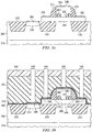
- FIGS 2 (a) to Figure 2 (d) are cross-sectional diagrams of a first embodiment of the instant invention. Illustrated in Figure 2 (a) is a MOS transistor formed using known integrated circuit manufacturing methods. As described above isolation regions 20 are formed in a semiconductor 10. A transistor gate stack comprising a gate dielectric layer 30 and a gate electrode 40 is formed on the surface of the semiconductor 10. The gate electrode usually comprises a conductive material such as doped polycrystalline silicon and various metals and silicides. Typical thicknesses for the transistor gate stack are between 800A and 5000A. Following the formation of the transistor gate stack a number of self-aligned implants are performed. These self-aligned implants include drain/source extension implant and pocket implants.
- the self-aligned implants that are aligned to the transistor gate stack will result in the formation of the doped regions 50 in the semiconductor 10.
- Sidewall structures 60 are formed adjacent to the gate electrode 40 using standard processing technology.
- the sidewall structures 60 typically comprise dielectric material such as silicon oxide, silicon nitride, or any other suitable dielectric material.
- the transistor source and drain regions 70 are formed by implanting suitable dopants into the semiconductor 10.
- metal silicide layers 80 and 90 are formed on the source and drain regions 70 and the gate electrode 40 respectively.
- a first dielectric layer comprising silicon oxide 130 is formed over the MOS transistor structure of Figure 2(a) as shown in Figure 2(b) .
- the first dielectric layer 130 is optional and is included to prevent the interaction of the gases used to form or etch subsequent layers with the underlying silicide layers 80 and 90.
- a second dielectric layer 140 is formed on the first dielectric layer 130 as shown in Figure 2(b) . In an embodiment that does not comprise the optional first dielectric layer 130, the second dielectric layer will be formed adjacent to the silicide layers 80 and 90.
- the second dielectric layer 140 comprises silicon carbide (SiC) in various crystalline and non-crystalline forms such as amorphous hydrogenated silicon carbide.
- the SiC layer can be formed using a plasma enhanced chemical vapor deposition (PECVD) method although any deposition process may be employed in accordance with the invention.
- PECVD plasma enhanced chemical vapor deposition
- the preferred SiC deposition process would use trimethylsilane as the silicon and carbon source, and a carrier gas of helium, wherein argon, for example, may also be used in place of helium.
- Examples of other possible source gasses include tetraethylsilane, and silane/methane. It has been found that when depositing with helium, the deposition rates are much reduced, and hence, the thickness of thin layers is more controllable. Even more importantly, the films tend to be more dense, and have lower hydrogen content, which significantly increases the film hardness and its resistance to chemical attack.
- the second dielectric layer 140 can comprise silicon oxycarbide, silicon carbonitride, silicon oxycarbonitride and boron carbide.
- a PMD layer 100 is formed over the second dielectric layer 140 and the MOS transistor structure is as shown in Figure 2(b) .
- a patterned photoresist layer 150 is formed on the PMD layer 100 that serves as an etch mask during the etching of the PMD layer 100 to form the openings 170.
- the etch process used to etch the PMD layer 100 is highly selective with an etch rate selectivity of at least 8 to 1 for The PMD dielectric 100 and the second dielectric layer 140 respectively. This high selectivity allows the openings above the source and drain regions 70 to be formed without completely removing the exposed region of the second dielectric layer 140 that lies above the gate electrode 40.
- the regions of the second dielectric layer 140 exposed in the openings 170 are removed using an etch process.
- the patterned photoresist layer 150 need not be removed before etching the exposed regions of the second dielectric layer 140. In other embodiments however it might be advantageous to remove the patterned photoresist layer 150 using standard semiconductor processing techniques before etching the second dielectric layer 140.
- the SiC layer can be etched using a reactive ion etching (RIE) process that comprises chlorine or fluorine.
- RIE reactive ion etching
- 1 to 10 percent of oxygen can be added to the RIE etch that comprises chlorine or fluorine.
- the RIE etch process will remove the exposed regions of the second dielectric layer 140 without significantly attacking the underlying layer.
- a second etch process is required to remove the exposed regions of the first dielectric layer 130 in the openings 170.
- the exposed regions of the first dielectric layer 130 can be removed using RIE or wet chemical etch processes. Following the removal of the exposed regions of the first and second dielectric regions 130 and 140 the structure is as shown in Figure 2(c) . If the patterned photoresist 150 is still present it is removed and conducting material can now be used to form electrical contacts to the MOS transistor gate electrode 40 and the source and drain regions 70.
- FIG. 2(d) This is illustrated in Figure 2(d) where conductive material such as a metal is used to form electrical contacts 180 to the MOS transistor source and drain regions 70 as well as an electrical contact 190 to the MOS transistor gate electrode 40.
- the first embodiment of the instant invention should not be confined to MOS transistor structure shown in Figures 2 (a) to 2(e).
- the first embodiment of the instant invention is applicable to any MOS transistor structure where the upper surface of the gate electrode is positioned above the upper surface of the source and drain regions.
- FIGS. 3 (a) to Figure 3 (c) are cross-sectional diagrams of a second embodiment of the instant invention. Illustrated in Figure 3(a) is a bipolar junction transistor (BJT) formed using known integrated circuit manufacturing methods.
- a highly doped buried layer 210 is formed in a semiconductor of a first conductivity type 200.
- Isolation regions 220 are formed in the semiconductor 200.
- a first silicon layer of a second conductivity type 240 is formed on the surface of the semiconductor 200 and will act as the base of the BJT.
- a highly doped region 230 is formed in the semiconductor 200 to provide electrical contact to the collector region of the BJT.
- Silicon oxide layers and silicon nitride layers are deposited and etched to form the silicon oxide 250 and silicon nitride 260 structures.
- a second silicon layer 265 of a first conductivity type is formed over the first silicon layer 240 and the silicon nitride structures 260 and will function as the emitter region of the BJT.
- the first conductivity type can be n-type and the second conductivity p-type or vice versa.
- Sidewall structures 270 are formed adjacent to the second silicon layer 265 and the silicon oxide 250 and silicon nitride 260 structures as shown in Figure 3(a) .
- Conductive layers 280, 290, and 295 are then formed on the regions of the first silicon layer 240, the second silicon layer 265 and the highly doped implanted region 230 to provide low contact resistance contacts to the base, emitter, and collector regions of the BJT respectively.
- These conductive layers 280, 290, and 295 can comprise a metal silicide or any other suitable conductive material.
- a first dielectric layer comprising silicon oxide 300 is formed over the BJT structure of Figure 3 (a) as shown in Figure 3(b) .
- the first dielectric layer 300 is optional and is included to prevent the interaction of the gases used to form or etch subsequent layers with the underlying layers.
- a second dielectric layer 310 is formed on the first dielectric layer 300 as shown in Figure 3(b) . In the embodiments that do not comprise the optional first dielectric layer 300, the second dielectric layer will be formed adjacent to the conductive layers 280, 290, and 295.
- the second dielectric layer 310 comprises silicon carbide (SiC) in various crystalline and non-crystalline forms such as amorphous hydrogenated silicon carbide.
- the SiC layer can be formed using a plasma enhanced chemical vapor deposition (PECVD) method although any deposition process may be employed in accordance with the invention.
- PECVD plasma enhanced chemical vapor deposition
- the preferred SiC deposition process would use trimethylsilane as the silicon and carbon source, and a carrier gas of helium, wherein argon, for example, may also be used in place of helium.
- Examples of other possible source gasses include tetraethylsilane, and silane/methane. It has been found that when depositing with helium, the deposition rates are much reduced, and hence, the thickness of thin layers is better controllable. Even more importantly, the films tend to be denser, and have lower hydrogen content, which significantly increases the film hardness and its resistance to chemical attack.
- the second dielectric layer 310 can comprise silicon oxycarbide, silicon carbonitride, silicon oxycarbonitride and boron carbide.
- a PMD layer 320 is formed over the second dielectric layer 310 and the BJT structure as shown in Figure 3(b) .
- a patterned photoresist layer 330 is formed on the PMD layer 320 that serves as an etch mask during the etching of the PMD layer 320 to form the openings 340.
- the etch process used to etch the PMD layer 320 is highly selective with an etch rate selectivity of at least 8 to 1 for the PMD dielectric 320 and the second dielectric layer 310 respectively.
- the regions of the second dielectric layer 310 exposed in the openings 340 are removed using an etch process.
- the patterned photoresist layer 330 need not be removed before etching the exposed regions of the second dielectric layer 310. In other embodiments however it might be advantageous to remove the patterned photoresist layer 330 using standard semiconductor processing techniques before etching the second dielectric layer 310.
- the SiC layer can be etched using a reactive ion etching (RIE) process that comprises chlorine or fluorine.
- RIE reactive ion etching
- 1 to 10 percent of oxygen can be added to the RIE etch that comprises chorine or fluorine. This etch process will remove the exposed regions of the second dielectric layer 310 without significantly attacking the underlying layers.
- a second etch process is required to remove the exposed regions of the first dielectric layer 300 in the openings 340.
- the exposed regions of the first dielectric layer 300 can be removed using RIE or wet chemical etch processes.
- the remaining patterned photoresist layer 330 is removed if present and conducting material is used to form electrical contacts to the BJT emitter, base and collector regions. This is illustrated in Figure 3(c) where conductive material such as a metal is used to form electrical contacts 360 to the base of the BJT as well as electrical contacts 350 and 370 to the emitter and collector regions of the BJT respectively.
- the second embodiment of the instant invention should not be confined to BJT structure shown in Figures 3(a) to 3(c) .
- the second embodiment of the instant invention is applicable to any BJT structure where the upper surface of the emitter region is above the upper surface of the base regions or above the upper surface of the collector region.
- FIGS. 4 (a) to Figure 4 (c) are cross-sectional diagrams of a third embodiment of the instant invention. Illustrated in Figure 4(a) is metal-oxide-metal capacitor formed using known integrated circuit manufacturing methods.
- An isolation region 410 is formed in a semiconductor.
- a polycrystalline silicon layer 420 is formed on the isolation structure 410 and sidewall structures 430 are formed adjacent to the polysilicon layer 410.
- a conductive layer 450 is formed on the polycrystalline layer 420 that will serve as the first plate of the capacitor.
- a dielectric layer 460 is formed over the conductive layer 450 as shown in Figure 4(a) . The dielectric layer 460 will function as the capacitor dielectric.
- a second conductive layer 470 is formed on the dielectric layer as shown in Figure 4(a) and will function as the second plate of the capacitor. It should be noted that the second conductive layer 470 does extend over the entire length of the polysilicon layer 420.
- a first dielectric layer comprising silicon oxide 480 is formed over the metal-oxide-metal capacitor structure of Figure 4 (a) as shown in Figure 4(b) .
- the first dielectric layer 480 is optional and is included to prevent the interaction of the gases used to form or etch subsequent layers with the underlying layers.
- a second dielectric layer 490 is formed on the first dielectric layer 480 as shown in Figure 4(b) . In the embodiments that do not comprise the optional first dielectric layer 480, the second dielectric layer 490 will be formed adjacent to the conductive layer 470.
- the second dielectric layer 490 comprises silicon carbide (SiC) in various crystalline and non-crystalline forms such as amorphous hydrogenated silicon carbide.
- the SiC layer can be formed using a plasma enhanced chemical vapor deposition (PECVD) method although any deposition process may be employed in accordance with the invention.
- PECVD plasma enhanced chemical vapor deposition
- the preferred SiC deposition process would use trimethylsilane as the silicon and carbon source, and a carrier gas of helium, wherein argon, for example, may also be used in place of helium.
- Examples of other possible source gasses include tetraethylsilane, and silane/methane. It has been found that when depositing with helium, the deposition rates are much reduced, and hence, the thickness of thin layers is better controllable. Even more importantly, the films tend to be denser, and have lower hydrogen content, which significantly increases the film hardness and its resistance to chemical attack.
- the second dielectric layer 490 can comprise silicon oxycarbide, silicon carbonitride, silicon oxycarbonitride and boron carbide.
- a PMD layer 500 is formed over the second dielectric layer 490 and the metal-oxide-metal capacitor structure as shown in Figure 4(b) .
- a patterned photoresist layer 510 is formed on the PMD layer 500 that serves as an etch mask during the etching of the PMD layer 500 to form the openings 520.
- the etch process used to etch the PMD layer 500 is highly selective with an etch rate selectivity of at least 8 to 1 for The PMD dielectric 500 and the second dielectric layer 490 respectively.
- the regions of the second dielectric layer 490 exposed in the openings 520 are removed using an etch process.
- the patterned photoresist layer 510 need not be removed before etching the exposed regions of the second dielectric layer 490. In other embodiments however it might be advantageous to remove the patterned photoresist layer 510 using standard semiconductor processing techniques before etching the second dielectric layer 490.
- the SiC layer can be etched using a reactive ion etching (RIE) process that comprises chlorine or fluorine.
- RIE reactive ion etching
- 1 to 10 percent of oxygen can be added to the RIE etch comprising chlorine or fluorine. This etch process will remove the exposed regions of the second dielectric layer 490 without significantly attacking the underlying layers.
- a second etch process is required to remove the exposed regions of the first dielectric layer 480 in the openings 520.
- the exposed regions of the first dielectric layer 480 can be removed using RIE or wet chemical etch processes.
- the patterned photoresist layer 510 is removed if still present, and conducting material is used to form electrical contacts to the metal regions of the metal-oxide-metal capacitor. This is illustrated in Figure 4(c) where conductive material such as a metal is used to form electrical contacts 530 and 540.
- the third embodiment of the instant invention should not be confined to metal-oxide-metal capacitor structure shown in Figures 4 (a) to 4(c).
- the third embodiment of the instant invention is applicable to any capacitor structure where electrical contacts are formed to the metal plates of the capacitor.
Landscapes
- Internal Circuitry In Semiconductor Integrated Circuit Devices (AREA)
- Electrodes Of Semiconductors (AREA)
- Bipolar Transistors (AREA)
- Semiconductor Integrated Circuits (AREA)
- Insulated Gate Type Field-Effect Transistor (AREA)
Abstract
Description
- This invention relates generally to the field of integrated circuit manufacturing and more particularly to a method for forming contacts to electronic devices.
- Integrated circuits comprise electronic devices such as transistors, resistors, and capacitors formed on a semiconductor substrate. The individual electronic devices are interconnected using a number of layers of metal interconnects formed in alternating dielectric layers above the surface of the semiconductor substrate containing the devices. Each electronic device that comprises the integrated circuit has to be connected to the metal lines through the dielectric layers that overlie the semiconductor substrate surface. Typically a pre-metal dielectric (PMD) layer is formed over the semiconductor substrate following the formation of the electronic devices in the semiconductor substrate. Electrical contact is made to the underlying electronic devices by forming openings in the PMD layer and filling the openings with a conductive plug formed using a conductive material such as titanium nitride, tungsten, or aluminum. The conductive plug (or plug) formed in the openings will allow an electrical connection to be made from the electronic devices to the various metal layers formed above the PMD layer. An example of such an electrical connection made to a typical metal oxide semiconductor (MOS) transistor is shown in
Figure 1 . - Shown in
Figure 1 is a typical MOS transistor fabricated using standard integrated circuit processing methodology.Isolation regions 20 are formed in asemiconductor 10. A transistor gate stack comprising a gatedielectric layer 30 and agate electrode 40 is formed on the surface of thesemiconductor 10. The gate electrode usually comprises a conductive material such as doped polycrystalline silicon and various metals and silicides. Typical thicknesses for the transistor gate stack are between 800A and 5000A. Following the formation of the transistor gate stack a number of self-aligned implants are performed. These self-aligned implants include drain/source extension implant and pocket implants. The self-aligned implants that are aligned to the transistor gate stack will result in the formation of thedoped regions 50 in thesemiconductor 10.Sidewall structures 60 are formed adjacent to thegate electrode 40 using standard processing technology. Thesidewall structures 60 typically comprise dielectric material such as silicon oxide, silicon nitride, or any other suitable dielectric material. Following the formation of thesidewall structures 60, the transistor source anddrain regions 70 are formed by implanting suitable dopants into thesemiconductor 10. Following the formation of the source anddrain regions 70,metal silicide layers drain regions 70 and thegate electrode 40 respectively. Themetal silicide layers PMD layer 100 is formed over the MOS transistor as shown in Figure and openings are 110 and 120 are formed in the PMD layer. Conductive plugs will be formed in the openings and the openings are formed using standard integrated circuit processing techniques. - Typically the
openings silicide layer 90 formed on thegate electrode 40 is about 800A to 5000A above thesilicide layer 80 formed on the source drain regions. This topographic variation makes performing the
contact etch down to the various silicide layers difficult. The different height of thevarious silicide layers deeper silicide layers 80 may cause the shallower contact etch (i.e. the etch to silicide layer 90) to continue throughsilicide layer 90 removing a significant portion of thesilicide layer 90. This problem is often addressed by reducing the etch times for forming thedeeper openings 110. However reducing the etch time for the deeper openings may lead to under-etched openings resulting in an increased contact resistance. - Topology variations across the wafer also require that the contact etch process contain about a 50% over-etch to ensure that all the openings across the semiconductor wafer are properly formed. This large over-etch results in large contact resistance variations across the semiconductor wafer that make it more difficult to form precision integrated circuits. In addition to the above described MOS transistor other devices such as bipolar junction transistors (BJT) and metal-insulator-metal (MIM) capacitors are also susceptible to the above described contact etch problems. There is therefore a need for a method of forming integrated circuits that reduces and/or eliminates the contact etch formation problems. The instant invention addresses this need.
- The instant invention is a method for forming electrical contacts to electronic devices formed as part of an integrated circuit. A conductive layer is formed on electronic device such as a MOS transistor, capacitor, or bipolar junction transistor. An optional first dielectric layer is formed over the conductive layer and a carbon containing dielectric layer formed over the optional dielectric layer if present. A PMD dielectric layer is formed over the carbon containing dielectric layer and openings are formed in the PMD layer. The openings are formed over the conductive layer, the optional dielectric layer, and the carbon containing dielectric layer. The exposed regions of the carbon containing dielectric layer and the optional dielectric layer (if present) are removed to expose the underlying conductive layer. A conductive material is then used to fill the opening and electrically contact the conductive layer formed on the electronic device.
- For a more complete understanding of the present invention and the advantages thereof, reference is now made to the following description taken in conjunction with the accompanying drawings, wherein like reference numerals represent like features, in which:
-
FIGURE 1 is a cross-sectional diagram showing a MOS transistor according to the prior art. -
FIGURE 2(a) - FIGURE 2(d) are cross-sectional diagrams showing an embodiment of the instant invention. -
FIGURE 3(a) - FIGURE 3(c) are cross-sectional diagrams showing an embodiment of the instant invention. -
FIGURE 4(a) - FIGURE 4 (c) are cross-sectional diagrams showing an embodiment of the instant invention. - Shown in
Figures 2 (a) toFigure 2 (d) are cross-sectional diagrams of a first embodiment of the instant invention. Illustrated inFigure 2 (a) is a MOS transistor formed using known integrated circuit manufacturing methods. As described aboveisolation regions 20 are formed in asemiconductor 10. A transistor gate stack comprising a gatedielectric layer 30 and agate electrode 40 is formed on the surface of thesemiconductor 10. The gate electrode usually comprises a conductive material such as doped polycrystalline silicon and various metals and silicides. Typical thicknesses for the transistor gate stack are between 800A and 5000A. Following the formation of the transistor gate stack a number of self-aligned implants are performed. These self-aligned implants include drain/source extension implant and pocket implants. The self-aligned implants that are aligned to the transistor gate stack will result in the formation of thedoped regions 50 in thesemiconductor 10.Sidewall structures 60 are formed adjacent to thegate electrode 40 using standard processing technology. Thesidewall structures 60 typically comprise dielectric material such as silicon oxide, silicon nitride, or any other suitable dielectric material. Following the formation of thesidewall structures 60, the transistor source and drainregions 70 are formed by implanting suitable dopants into thesemiconductor 10. Following the formation of the source and drainregions 70, metal silicide layers 80 and 90 and formed on the source and drainregions 70 and thegate electrode 40 respectively. - A first dielectric layer comprising
silicon oxide 130 is formed over the MOS transistor structure ofFigure 2(a) as shown inFigure 2(b) . Thefirst dielectric layer 130 is optional and is included to prevent the interaction of the gases used to form or etch subsequent layers with the underlying silicide layers 80 and 90. Asecond dielectric layer 140 is formed on thefirst dielectric layer 130 as shown inFigure 2(b) . In an embodiment that does not comprise the optional firstdielectric layer 130, the second dielectric layer will be formed adjacent to the silicide layers 80 and 90. In an embodiment of the instant invention thesecond dielectric layer 140 comprises silicon carbide (SiC) in various crystalline and non-crystalline forms such as amorphous hydrogenated silicon carbide. The SiC layer can be formed using a plasma enhanced chemical vapor deposition (PECVD) method although any deposition process may be employed in accordance with the invention. The preferred SiC deposition process would use trimethylsilane as the silicon and carbon source, and a carrier gas of helium, wherein argon, for example, may also be used in place of helium. Examples of other possible source gasses include tetraethylsilane, and silane/methane. It has been found that when depositing with helium, the deposition rates are much reduced, and hence, the thickness of thin layers is more controllable. Even more importantly, the films tend to be more dense, and have lower hydrogen content, which significantly increases the film hardness and its resistance to chemical attack. This then reduces the etchability of this material, and improves etch selectivity of silicon oxide to SiC. In other embodiments thesecond dielectric layer 140 can comprise silicon oxycarbide, silicon carbonitride, silicon oxycarbonitride and boron carbide. - Following the formation of the second dielectric layer 140 a
PMD layer 100 is formed over thesecond dielectric layer 140 and the MOS transistor structure is as shown inFigure 2(b) . A patternedphotoresist layer 150 is formed on thePMD layer 100 that serves as an etch mask during the etching of thePMD layer 100 to form theopenings 170. The etch process used to etch thePMD layer 100 is highly selective with an etch rate selectivity of at least 8 to 1 for The PMD dielectric 100 and thesecond dielectric layer 140 respectively. This high selectivity allows the openings above the source and drainregions 70 to be formed without completely removing the exposed region of thesecond dielectric layer 140 that lies above thegate electrode 40. Following the formation of theopenings 170 the regions of thesecond dielectric layer 140 exposed in theopenings 170 are removed using an etch process. The patternedphotoresist layer 150 need not be removed before etching the exposed regions of thesecond dielectric layer 140. In other embodiments however it might be advantageous to remove the patternedphotoresist layer 150 using standard semiconductor processing techniques before etching thesecond dielectric layer 140. In an embodiment where thesecond dielectric layer 140 comprises SiC, the SiC layer can be etched using a reactive ion etching (RIE) process that comprises chlorine or fluorine. In a further embodiment of the SiC RIE etch process, 1 to 10 percent of oxygen can be added to the RIE etch that comprises chlorine or fluorine. The RIE etch process will remove the exposed regions of thesecond dielectric layer 140 without significantly attacking the underlying layer. In the embodiment of the instant invention that comprises the optional first dielectric layer 130 a second etch process is required to remove the exposed regions of thefirst dielectric layer 130 in theopenings 170. The exposed regions of thefirst dielectric layer 130 can be removed using RIE or wet chemical etch processes. Following the removal of the exposed regions of the first and seconddielectric regions Figure 2(c) . If the patternedphotoresist 150 is still present it is removed and conducting material can now be used to form electrical contacts to the MOStransistor gate electrode 40 and the source and drainregions 70. This is illustrated inFigure 2(d) where conductive material such as a metal is used to formelectrical contacts 180 to the MOS transistor source and drainregions 70 as well as anelectrical contact 190 to the MOStransistor gate electrode 40. The first embodiment of the instant invention should not be confined to MOS transistor structure shown inFigures 2 (a) to 2(e). The first embodiment of the instant invention is applicable to any MOS transistor structure where the upper surface of the gate electrode is positioned above the upper surface of the source and drain regions. - Shown in
Figures 3 (a) toFigure 3 (c) are cross-sectional diagrams of a second embodiment of the instant invention. Illustrated inFigure 3(a) is a bipolar junction transistor (BJT) formed using known integrated circuit manufacturing methods. A highly doped buriedlayer 210 is formed in a semiconductor of afirst conductivity type 200.Isolation regions 220 are formed in thesemiconductor 200. A first silicon layer of asecond conductivity type 240 is formed on the surface of thesemiconductor 200 and will act as the base of the BJT. A highly dopedregion 230 is formed in thesemiconductor 200 to provide electrical contact to the collector region of the BJT. Silicon oxide layers and silicon nitride layers are deposited and etched to form thesilicon oxide 250 andsilicon nitride 260 structures. Asecond silicon layer 265 of a first conductivity type is formed over thefirst silicon layer 240 and thesilicon nitride structures 260 and will function as the emitter region of the BJT. In the BJT structure shown inFigure 3 (a) the first conductivity type can be n-type and the second conductivity p-type or vice versa.Sidewall structures 270 are formed adjacent to thesecond silicon layer 265 and thesilicon oxide 250 andsilicon nitride 260 structures as shown inFigure 3(a) .Conductive layers first silicon layer 240, thesecond silicon layer 265 and the highly doped implantedregion 230 to provide low contact resistance contacts to the base, emitter, and collector regions of the BJT respectively. Theseconductive layers - A first dielectric layer comprising
silicon oxide 300 is formed over the BJT structure ofFigure 3 (a) as shown inFigure 3(b) . Thefirst dielectric layer 300 is optional and is included to prevent the interaction of the gases used to form or etch subsequent layers with the underlying layers. Asecond dielectric layer 310 is formed on thefirst dielectric layer 300 as shown inFigure 3(b) . In the embodiments that do not comprise the optional firstdielectric layer 300, the second dielectric layer will be formed adjacent to theconductive layers second dielectric layer 310 comprises silicon carbide (SiC) in various crystalline and non-crystalline forms such as amorphous hydrogenated silicon carbide. The SiC layer can be formed using a plasma enhanced chemical vapor deposition (PECVD) method although any deposition process may be employed in accordance with the invention. The preferred SiC deposition process would use trimethylsilane as the silicon and carbon source, and a carrier gas of helium, wherein argon, for example, may also be used in place of helium. Examples of other possible source gasses include tetraethylsilane, and silane/methane. It has been found that when depositing with helium, the deposition rates are much reduced, and hence, the thickness of thin layers is better controllable. Even more importantly, the films tend to be denser, and have lower hydrogen content, which significantly increases the film hardness and its resistance to chemical attack. This then reduces the etchability of this material, and improves etch selectivity of silicon oxide to SiC. In other embodiments thesecond dielectric layer 310 can comprise silicon oxycarbide, silicon carbonitride, silicon oxycarbonitride and boron carbide. - Following the formation of the second dielectric layer 310 a
PMD layer 320 is formed over thesecond dielectric layer 310 and the BJT structure as shown inFigure 3(b) . A patternedphotoresist layer 330 is formed on thePMD layer 320 that serves as an etch mask during the etching of thePMD layer 320 to form theopenings 340. The etch process used to etch thePMD layer 320 is highly selective with an etch rate selectivity of at least 8 to 1 for thePMD dielectric 320 and thesecond dielectric layer 310 respectively. Following the formation of theopenings 340 the regions of thesecond dielectric layer 310 exposed in theopenings 340 are removed using an etch process. The patternedphotoresist layer 330 need not be removed before etching the exposed regions of thesecond dielectric layer 310. In other embodiments however it might be advantageous to remove the patternedphotoresist layer 330 using standard semiconductor processing techniques before etching thesecond dielectric layer 310. In an embodiment where thesecond dielectric layer 310 comprises SiC, the SiC layer can be etched using a reactive ion etching (RIE) process that comprises chlorine or fluorine. In a further embodiment of the SiC RIE etch process, 1 to 10 percent of oxygen can be added to the RIE etch that comprises chorine or fluorine. This etch process will remove the exposed regions of thesecond dielectric layer 310 without significantly attacking the underlying layers. In the embodiment of the instant invention that comprises the optional firstdielectric layer 300, a second etch process is required to remove the exposed regions of thefirst dielectric layer 300 in theopenings 340. The exposed regions of thefirst dielectric layer 300 can be removed using RIE or wet chemical etch processes. Following the removal of the exposed regions of the first and seconddielectric regions photoresist layer 330 is removed if present and conducting material is used to form electrical contacts to the BJT emitter, base and collector regions. This is illustrated inFigure 3(c) where conductive material such as a metal is used to formelectrical contacts 360 to the base of the BJT as well aselectrical contacts Figures 3(a) to 3(c) . The second embodiment of the instant invention is applicable to any BJT structure where the upper surface of the emitter region is above the upper surface of the base regions or above the upper surface of the collector region. - Shown in
Figures 4 (a) to Figure 4 (c) are cross-sectional diagrams of a third embodiment of the instant invention. Illustrated inFigure 4(a) is metal-oxide-metal capacitor formed using known integrated circuit manufacturing methods. Anisolation region 410 is formed in a semiconductor. Apolycrystalline silicon layer 420 is formed on theisolation structure 410 andsidewall structures 430 are formed adjacent to thepolysilicon layer 410. Aconductive layer 450 is formed on thepolycrystalline layer 420 that will serve as the first plate of the capacitor. Adielectric layer 460 is formed over theconductive layer 450 as shown inFigure 4(a) . Thedielectric layer 460 will function as the capacitor dielectric. A secondconductive layer 470 is formed on the dielectric layer as shown inFigure 4(a) and will function as the second plate of the capacitor. It should be noted that the secondconductive layer 470 does extend over the entire length of thepolysilicon layer 420. - A first dielectric layer comprising
silicon oxide 480 is formed over the metal-oxide-metal capacitor structure ofFigure 4 (a) as shown inFigure 4(b) . Thefirst dielectric layer 480 is optional and is included to prevent the interaction of the gases used to form or etch subsequent layers with the underlying layers. Asecond dielectric layer 490 is formed on thefirst dielectric layer 480 as shown inFigure 4(b) . In the embodiments that do not comprise the optional firstdielectric layer 480, thesecond dielectric layer 490 will be formed adjacent to theconductive layer 470. In an embodiment of the instant invention thesecond dielectric layer 490 comprises silicon carbide (SiC) in various crystalline and non-crystalline forms such as amorphous hydrogenated silicon carbide. The SiC layer can be formed using a plasma enhanced chemical vapor deposition (PECVD) method although any deposition process may be employed in accordance with the invention. The preferred SiC deposition process would use trimethylsilane as the silicon and carbon source, and a carrier gas of helium, wherein argon, for example, may also be used in place of helium. Examples of other possible source gasses include tetraethylsilane, and silane/methane. It has been found that when depositing with helium, the deposition rates are much reduced, and hence, the thickness of thin layers is better controllable. Even more importantly, the films tend to be denser, and have lower hydrogen content, which significantly increases the film hardness and its resistance to chemical attack. This then reduces the etchability of this material, and improves etch selectivity of silicon oxide to SiC. In other embodiments thesecond dielectric layer 490 can comprise silicon oxycarbide, silicon carbonitride, silicon oxycarbonitride and boron carbide. - Following the formation of the
second dielectric layer 490, aPMD layer 500 is formed over thesecond dielectric layer 490 and the metal-oxide-metal capacitor structure as shown inFigure 4(b) . A patternedphotoresist layer 510 is formed on thePMD layer 500 that serves as an etch mask during the etching of thePMD layer 500 to form theopenings 520. The etch process used to etch thePMD layer 500 is highly selective with an etch rate selectivity of at least 8 to 1 for The PMD dielectric 500 and thesecond dielectric layer 490 respectively. Following the formation of theopenings 520, the regions of thesecond dielectric layer 490 exposed in theopenings 520 are removed using an etch process. The patternedphotoresist layer 510 need not be removed before etching the exposed regions of thesecond dielectric layer 490. In other embodiments however it might be advantageous to remove the patternedphotoresist layer 510 using standard semiconductor processing techniques before etching thesecond dielectric layer 490. In an embodiment where thesecond dielectric layer 490 comprises SiC, the SiC layer can be etched using a reactive ion etching (RIE) process that comprises chlorine or fluorine. In a further embodiment of the SiC RIE etch process, 1 to 10 percent of oxygen can be added to the RIE etch comprising chlorine or fluorine. This etch process will remove the exposed regions of thesecond dielectric layer 490 without significantly attacking the underlying layers. In the embodiment of the instant invention that comprises the optional firstdielectric layer 480, a second etch process is required to remove the exposed regions of thefirst dielectric layer 480 in theopenings 520. The exposed regions of thefirst dielectric layer 480 can be removed using RIE or wet chemical etch processes. Following the removal of the exposed regions of the first and seconddielectric regions photoresist layer 510 is removed if still present, and conducting material is used to form electrical contacts to the metal regions of the metal-oxide-metal capacitor. This is illustrated inFigure 4(c) where conductive material such as a metal is used to formelectrical contacts Figures 4 (a) to 4(c). The third embodiment of the instant invention is applicable to any capacitor structure where electrical contacts are formed to the metal plates of the capacitor. - While this invention has been described with reference to illustrative embodiments, this description is not intended to be construed in a limiting sense. Various modifications and combinations of the illustrative embodiments, as well as other embodiments of the invention will be apparent to persons skilled in the art upon reference to the description. It is therefore intended that the appended claims encompass any such modifications or embodiments.
Claims (10)
- A method for forming an integrated circuit capacitor, comprising:forming a first conductive layer (450) over a semiconductor;forming a first dielectric layer (460) over said first conductive layer;forming a second patterned conductive layer (470) over said first dielectric layer and said first conductive layer;forming a second dielectric layer (480) over said second patterned conductive layer;forming a third dielectric layer (490) comprising carbon over said second patterned conductive layer;forming a PMD dielectric layer (500) over said third dielectric layer and said second patterned conductive layer;forming at least one first and second openings (520) in said PMD dielectric layer over said second patterned conductive layer thereby exposing regions of said third dielectric layer, each opening formed to a different depth;removing said exposed region of said third dielectric layer thereby exposing regions of said second dielectric layer;removing said exposed region of said second dielectric layer; andforming a third conductive region (530) in said opening of said PMD layer wherein said first conductive region contacts said second patterned conductive layer.
- The method of claim 1 wherein said third dielectric layer is formed from a material selected from the group consisting of silicon carbide, silicon oxycarbide, silicon carbonitride, silicon oxycarbonitride and boron carbide.
- The method of claim 1 or claim 2 wherein said removing said exposed region of said third dielectric layer comprises using a RIE etch comprising chlorine.
- A method of forming an integrated circuit, comprising:forming a conductive layer (80,90) over first (80) and second (90) regions of a semiconductor (10);forming a dielectric layer (140) comprising carbon over said conductive layer;forming a PMD dielectric layer (100) over said dielectric layer and said conductive layer;forming first and second openings (170) in said PMD dielectric layer over said conductive layer thereby exposing regions of said dielectric layer, each opening formed to a different depth;removing said exposed regions of said dielectric layer; andforming first (110) and second (120) conductive regions in said opening of said PMD layer wherein said first and second conductive regions contact said conductive layer.
- The method of claim 4 wherein said dielectric layer is formed from a material selected from the group consisting of silicon carbide, silicon oxycarbide, silicon carbonitride, silicon oxycarbonitride and boron carbide.
- The method of claim 4 or claim 5 wherein said removing said exposed regions of said dielectric layer comprises using a RIE etch comprising chlorine.
- The method of claim 4, claim 5, or claim 6 further comprising forming a second dielectric layer (130) between said conductive layer and said dielectric layer.
- A method of forming integrated circuit contacts, comprising:forming a conductive layer (310) over first (280) and second (290, 295) regions of a semiconductor;forming a first dielectric layer (300) over said conductive layer;forming a second dielectric layer (310) comprising carbon over said first conductive layer;forming a PMD dielectric layer (320) over said second dielectric layer and said conductive layer;forming at least one first and second openings (340) in said PMD dielectric layer over said conductive layer thereby exposing regions of said second dielectric layer, each opening formed to a different depth;removing said exposed regions of said second dielectric layer thereby exposing regions of said first dielectric layer;removing said exposed regions of said first dielectric layer; andforming first (350) and second (360, 370) conductive regions in said opening of said PMD layer wherein said first and second conductive regions contact said conductive layer.
- The method of claim 8 wherein said second dielectric layer is formed from a material selected from the group consisting of silicon carbide, silicon oxycarbide, silicon carbonitride, silicon oxycarbonitride and boron carbide.
- The method of claim 8 or claim 9 wherein said removing said exposed regions of said second dielectric layer comprises using a RIE etch comprising chlorine.
Applications Claiming Priority (2)
| Application Number | Priority Date | Filing Date | Title |
|---|---|---|---|
| US10/350,691 US6833300B2 (en) | 2003-01-24 | 2003-01-24 | Method of forming integrated circuit contacts |
| EP04100236A EP1498939A3 (en) | 2003-01-24 | 2004-01-23 | Method of forming integrated circuit contacts |
Related Parent Applications (1)
| Application Number | Title | Priority Date | Filing Date |
|---|---|---|---|
| EP04100236A Division EP1498939A3 (en) | 2003-01-24 | 2004-01-23 | Method of forming integrated circuit contacts |
Publications (2)
| Publication Number | Publication Date |
|---|---|
| EP3142145A1 true EP3142145A1 (en) | 2017-03-15 |
| EP3142145B1 EP3142145B1 (en) | 2022-10-12 |
Family
ID=32735624
Family Applications (2)
| Application Number | Title | Priority Date | Filing Date |
|---|---|---|---|
| EP16191250.6A Expired - Lifetime EP3142145B1 (en) | 2003-01-24 | 2004-01-23 | Method of forming integrated circuit contacts |
| EP04100236A Ceased EP1498939A3 (en) | 2003-01-24 | 2004-01-23 | Method of forming integrated circuit contacts |
Family Applications After (1)
| Application Number | Title | Priority Date | Filing Date |
|---|---|---|---|
| EP04100236A Ceased EP1498939A3 (en) | 2003-01-24 | 2004-01-23 | Method of forming integrated circuit contacts |
Country Status (3)
| Country | Link |
|---|---|
| US (2) | US6833300B2 (en) |
| EP (2) | EP3142145B1 (en) |
| JP (1) | JP2004228584A (en) |
Families Citing this family (7)
| Publication number | Priority date | Publication date | Assignee | Title |
|---|---|---|---|---|
| US7775917B2 (en) * | 2005-08-08 | 2010-08-17 | Lifetime Products, Inc. | Basketball system |
| US20070210421A1 (en) * | 2006-03-13 | 2007-09-13 | Texas Instruments Inc. | Semiconductor device fabricated using a carbon-containing film as a contact etch stop layer |
| US8021975B2 (en) * | 2007-07-24 | 2011-09-20 | Tokyo Electron Limited | Plasma processing method for forming a film and an electronic component manufactured by the method |
| US7700424B2 (en) * | 2008-02-27 | 2010-04-20 | Applied Materials, Inc. | Method of forming an embedded silicon carbon epitaxial layer |
| KR101009395B1 (en) * | 2008-08-06 | 2011-01-19 | 주식회사 동부하이텍 | Transistor of image sensor and manufacturing method thereof |
| US8106383B2 (en) * | 2009-11-13 | 2012-01-31 | International Business Machines Corporation | Self-aligned graphene transistor |
| US9093380B2 (en) | 2013-06-05 | 2015-07-28 | Texas Instruments Incorporated | Dielectric liner added after contact etch before silicide formation |
Citations (6)
| Publication number | Priority date | Publication date | Assignee | Title |
|---|---|---|---|---|
| JPH10321838A (en) * | 1997-05-16 | 1998-12-04 | Matsushita Electric Ind Co Ltd | Method for manufacturing semiconductor device |
| JP2000150791A (en) * | 1998-11-11 | 2000-05-30 | Nec Corp | Method of manufacturing semiconductor device and semiconductor device |
| WO2000067304A1 (en) * | 1999-05-03 | 2000-11-09 | Interuniversitair Microelektronica Centrum (Imec) | Method for removal of sic |
| US6261892B1 (en) * | 1999-12-31 | 2001-07-17 | Texas Instruments Incorporated | Intra-chip AC isolation of RF passive components |
| US20020076918A1 (en) * | 2000-07-19 | 2002-06-20 | Chartered Semiconductor Manufacturing Ltd. | Use of boron carbide as an etch-stop and barrier layer for copper dual damascene metallization |
| US20020094656A1 (en) * | 2001-01-17 | 2002-07-18 | International Business Machines Corporation | Metal-insulator-metal capacitor in copper |
Family Cites Families (10)
| Publication number | Priority date | Publication date | Assignee | Title |
|---|---|---|---|---|
| JPH08236619A (en) * | 1995-02-27 | 1996-09-13 | Mitsubishi Electric Corp | Semiconductor device and method of manufacturing semiconductor device |
| US6136700A (en) * | 1996-12-20 | 2000-10-24 | Texas Instruments Incorporated | Method for enhancing the performance of a contact |
| KR20000016942A (en) * | 1998-08-07 | 2000-03-25 | 클라크 3세 존 엠. | Method for rorming a gate contact directly over the channel region of a mos transistor |
| GB2357186A (en) * | 1999-08-27 | 2001-06-13 | Lucent Technologies Inc | Self-aligned contact process involving forming an opening in carbide or nitride layer over a gate |
| US6236091B1 (en) * | 1999-09-30 | 2001-05-22 | Advanced Micro Devices, Inc. | Method of forming a local interconnect with improved etch selectivity of silicon dioxide/silicide |
| EP1183724A1 (en) * | 2000-03-13 | 2002-03-06 | Koninklijke Philips Electronics N.V. | A method of manufacturing a semiconductor device |
| US6362094B1 (en) * | 2000-08-16 | 2002-03-26 | Agere Systems Guardian Corp. | Hydrogenated silicon carbide as a liner for self-aligning contact vias |
| JP2002289594A (en) * | 2001-03-28 | 2002-10-04 | Nec Corp | Semiconductor device and method of manufacturing the same |
| US6444566B1 (en) * | 2001-04-30 | 2002-09-03 | Taiwan Semiconductor Manufacturing Company | Method of making borderless contact having a sion buffer layer |
| KR100442863B1 (en) * | 2001-08-01 | 2004-08-02 | 삼성전자주식회사 | Method for fabricating semiconductor device having metal-insulator-metal capacitor and damascene wiring structure |
-
2003
- 2003-01-24 US US10/350,691 patent/US6833300B2/en not_active Expired - Lifetime
-
2004
- 2004-01-23 EP EP16191250.6A patent/EP3142145B1/en not_active Expired - Lifetime
- 2004-01-23 JP JP2004015316A patent/JP2004228584A/en active Pending
- 2004-01-23 EP EP04100236A patent/EP1498939A3/en not_active Ceased
- 2004-10-08 US US10/962,048 patent/US7087479B2/en not_active Expired - Lifetime
Patent Citations (6)
| Publication number | Priority date | Publication date | Assignee | Title |
|---|---|---|---|---|
| JPH10321838A (en) * | 1997-05-16 | 1998-12-04 | Matsushita Electric Ind Co Ltd | Method for manufacturing semiconductor device |
| JP2000150791A (en) * | 1998-11-11 | 2000-05-30 | Nec Corp | Method of manufacturing semiconductor device and semiconductor device |
| WO2000067304A1 (en) * | 1999-05-03 | 2000-11-09 | Interuniversitair Microelektronica Centrum (Imec) | Method for removal of sic |
| US6261892B1 (en) * | 1999-12-31 | 2001-07-17 | Texas Instruments Incorporated | Intra-chip AC isolation of RF passive components |
| US20020076918A1 (en) * | 2000-07-19 | 2002-06-20 | Chartered Semiconductor Manufacturing Ltd. | Use of boron carbide as an etch-stop and barrier layer for copper dual damascene metallization |
| US20020094656A1 (en) * | 2001-01-17 | 2002-07-18 | International Business Machines Corporation | Metal-insulator-metal capacitor in copper |
Also Published As
| Publication number | Publication date |
|---|---|
| EP1498939A3 (en) | 2006-01-04 |
| EP3142145B1 (en) | 2022-10-12 |
| US6833300B2 (en) | 2004-12-21 |
| US20040147110A1 (en) | 2004-07-29 |
| US7087479B2 (en) | 2006-08-08 |
| JP2004228584A (en) | 2004-08-12 |
| US20050064692A1 (en) | 2005-03-24 |
| EP1498939A2 (en) | 2005-01-19 |
Similar Documents
| Publication | Publication Date | Title |
|---|---|---|
| US6198144B1 (en) | Passivation of sidewalls of a word line stack | |
| US6476488B1 (en) | Method for fabricating borderless and self-aligned polysilicon and metal contact landing plugs for multilevel interconnections | |
| KR0179677B1 (en) | Semiconductor device wiring or electrode | |
| US5767004A (en) | Method for forming a low impurity diffusion polysilicon layer | |
| US6614082B1 (en) | Fabrication of semiconductor devices with transition metal boride films as diffusion barriers | |
| US5899741A (en) | Method of manufacturing low resistance and low junction leakage contact | |
| US20260096424A1 (en) | Integration scheme to build resistor, capacitor, efuse using silicon-rich dielectric layer as a base dielectric | |
| JP2002543610A (en) | Removal method of SiC | |
| US6762110B1 (en) | Method of manufacturing semiconductor device having capacitor | |
| US6833300B2 (en) | Method of forming integrated circuit contacts | |
| JP2002124649A (en) | Semiconductor integrated circuit device and method of manufacturing the same | |
| US6797596B2 (en) | Sacrificial deposition layer as screening material for implants into a wafer during the manufacture of a semiconductor device | |
| US8541822B2 (en) | Semiconductor device and method for producing the same | |
| JP4257343B2 (en) | Manufacturing method of semiconductor device | |
| US20250221015A1 (en) | Integrated deep trench high-k capacitor and method | |
| KR100291415B1 (en) | Method for manufacturing contact of semiconductor device | |
| JP3361971B2 (en) | Metal nitride conversion method and semiconductor device manufacturing method | |
| KR101255764B1 (en) | Method of manufacturing a capacitor in a semiconductor device | |
| JP5646116B1 (en) | Semiconductor device manufacturing method and semiconductor device | |
| JP6405026B2 (en) | Semiconductor device manufacturing method and semiconductor device | |
| KR100192184B1 (en) | Contact Plug Manufacturing Method | |
| JP6501819B2 (en) | Semiconductor device manufacturing method and semiconductor device | |
| KR100447976B1 (en) | A method for manufacturing capacitor of semiconductor device | |
| KR100853459B1 (en) | Method of reducing contact resistance of semiconductor device | |
| KR20020052455A (en) | Manufacturing method for semiconductor device |
Legal Events
| Date | Code | Title | Description |
|---|---|---|---|
| PUAI | Public reference made under article 153(3) epc to a published international application that has entered the european phase |
Free format text: ORIGINAL CODE: 0009012 |
|
| STAA | Information on the status of an ep patent application or granted ep patent |
Free format text: STATUS: THE APPLICATION HAS BEEN PUBLISHED |
|
| AC | Divisional application: reference to earlier application |
Ref document number: 1498939 Country of ref document: EP Kind code of ref document: P |
|
| AK | Designated contracting states |
Kind code of ref document: A1 Designated state(s): DE FR GB |
|
| STAA | Information on the status of an ep patent application or granted ep patent |
Free format text: STATUS: REQUEST FOR EXAMINATION WAS MADE |
|
| 17P | Request for examination filed |
Effective date: 20170915 |
|
| RBV | Designated contracting states (corrected) |
Designated state(s): DE FR GB |
|
| STAA | Information on the status of an ep patent application or granted ep patent |
Free format text: STATUS: EXAMINATION IS IN PROGRESS |
|
| 17Q | First examination report despatched |
Effective date: 20210122 |
|
| REG | Reference to a national code |
Ref country code: DE Ref legal event code: R079 Ref document number: 602004055111 Country of ref document: DE Free format text: PREVIOUS MAIN CLASS: H01L0023522000 Ipc: H01L0021768000 |
|
| RIC1 | Information provided on ipc code assigned before grant |
Ipc: H01L 23/532 20060101ALI20220317BHEP Ipc: H01L 23/522 20060101ALI20220317BHEP Ipc: H01L 21/768 20060101AFI20220317BHEP |
|
| GRAP | Despatch of communication of intention to grant a patent |
Free format text: ORIGINAL CODE: EPIDOSNIGR1 |
|
| STAA | Information on the status of an ep patent application or granted ep patent |
Free format text: STATUS: GRANT OF PATENT IS INTENDED |
|
| INTG | Intention to grant announced |
Effective date: 20220426 |
|
| GRAS | Grant fee paid |
Free format text: ORIGINAL CODE: EPIDOSNIGR3 |
|
| GRAA | (expected) grant |
Free format text: ORIGINAL CODE: 0009210 |
|
| STAA | Information on the status of an ep patent application or granted ep patent |
Free format text: STATUS: THE PATENT HAS BEEN GRANTED |
|
| AC | Divisional application: reference to earlier application |
Ref document number: 1498939 Country of ref document: EP Kind code of ref document: P |
|
| AK | Designated contracting states |
Kind code of ref document: B1 Designated state(s): DE FR GB |
|
| REG | Reference to a national code |
Ref country code: GB Ref legal event code: FG4D |
|
| REG | Reference to a national code |
Ref country code: DE Ref legal event code: R096 Ref document number: 602004055111 Country of ref document: DE |
|
| PGFP | Annual fee paid to national office [announced via postgrant information from national office to epo] |
Ref country code: GB Payment date: 20221221 Year of fee payment: 20 Ref country code: FR Payment date: 20221220 Year of fee payment: 20 |
|
| PGFP | Annual fee paid to national office [announced via postgrant information from national office to epo] |
Ref country code: DE Payment date: 20221220 Year of fee payment: 20 |
|
| P01 | Opt-out of the competence of the unified patent court (upc) registered |
Effective date: 20230523 |
|
| REG | Reference to a national code |
Ref country code: DE Ref legal event code: R097 Ref document number: 602004055111 Country of ref document: DE |
|
| PLBE | No opposition filed within time limit |
Free format text: ORIGINAL CODE: 0009261 |
|
| STAA | Information on the status of an ep patent application or granted ep patent |
Free format text: STATUS: NO OPPOSITION FILED WITHIN TIME LIMIT |
|
| 26N | No opposition filed |
Effective date: 20230713 |
|
| REG | Reference to a national code |
Ref country code: DE Ref legal event code: R071 Ref document number: 602004055111 Country of ref document: DE |
|
| REG | Reference to a national code |
Ref country code: GB Ref legal event code: PE20 Expiry date: 20240122 |
|
| PG25 | Lapsed in a contracting state [announced via postgrant information from national office to epo] |
Ref country code: GB Free format text: LAPSE BECAUSE OF EXPIRATION OF PROTECTION Effective date: 20240122 |