EP3142103A1 - Display device - Google Patents
Display device Download PDFInfo
- Publication number
- EP3142103A1 EP3142103A1 EP16187911.9A EP16187911A EP3142103A1 EP 3142103 A1 EP3142103 A1 EP 3142103A1 EP 16187911 A EP16187911 A EP 16187911A EP 3142103 A1 EP3142103 A1 EP 3142103A1
- Authority
- EP
- European Patent Office
- Prior art keywords
- bridges
- connection
- display device
- wires
- connection wire
- Prior art date
- Legal status (The legal status is an assumption and is not a legal conclusion. Google has not performed a legal analysis and makes no representation as to the accuracy of the status listed.)
- Granted
Links
Images






Classifications
-
- H—ELECTRICITY
- H10—SEMICONDUCTOR DEVICES; ELECTRIC SOLID-STATE DEVICES NOT OTHERWISE PROVIDED FOR
- H10K—ORGANIC ELECTRIC SOLID-STATE DEVICES
- H10K59/00—Integrated devices, or assemblies of multiple devices, comprising at least one organic light-emitting element covered by group H10K50/00
- H10K59/10—OLED displays
-
- H—ELECTRICITY
- H10—SEMICONDUCTOR DEVICES; ELECTRIC SOLID-STATE DEVICES NOT OTHERWISE PROVIDED FOR
- H10K—ORGANIC ELECTRIC SOLID-STATE DEVICES
- H10K59/00—Integrated devices, or assemblies of multiple devices, comprising at least one organic light-emitting element covered by group H10K50/00
- H10K59/10—OLED displays
- H10K59/12—Active-matrix OLED [AMOLED] displays
- H10K59/131—Interconnections, e.g. wiring lines or terminals
-
- G—PHYSICS
- G02—OPTICS
- G02F—OPTICAL DEVICES OR ARRANGEMENTS FOR THE CONTROL OF LIGHT BY MODIFICATION OF THE OPTICAL PROPERTIES OF THE MEDIA OF THE ELEMENTS INVOLVED THEREIN; NON-LINEAR OPTICS; FREQUENCY-CHANGING OF LIGHT; OPTICAL LOGIC ELEMENTS; OPTICAL ANALOGUE/DIGITAL CONVERTERS
- G02F1/00—Devices or arrangements for the control of the intensity, colour, phase, polarisation or direction of light arriving from an independent light source, e.g. switching, gating or modulating; Non-linear optics
- G02F1/01—Devices or arrangements for the control of the intensity, colour, phase, polarisation or direction of light arriving from an independent light source, e.g. switching, gating or modulating; Non-linear optics for the control of the intensity, phase, polarisation or colour
- G02F1/13—Devices or arrangements for the control of the intensity, colour, phase, polarisation or direction of light arriving from an independent light source, e.g. switching, gating or modulating; Non-linear optics for the control of the intensity, phase, polarisation or colour based on liquid crystals, e.g. single liquid crystal display cells
- G02F1/133—Constructional arrangements; Operation of liquid crystal cells; Circuit arrangements
- G02F1/1333—Constructional arrangements; Manufacturing methods
- G02F1/1345—Conductors connecting electrodes to cell terminals
-
- G—PHYSICS
- G02—OPTICS
- G02F—OPTICAL DEVICES OR ARRANGEMENTS FOR THE CONTROL OF LIGHT BY MODIFICATION OF THE OPTICAL PROPERTIES OF THE MEDIA OF THE ELEMENTS INVOLVED THEREIN; NON-LINEAR OPTICS; FREQUENCY-CHANGING OF LIGHT; OPTICAL LOGIC ELEMENTS; OPTICAL ANALOGUE/DIGITAL CONVERTERS
- G02F1/00—Devices or arrangements for the control of the intensity, colour, phase, polarisation or direction of light arriving from an independent light source, e.g. switching, gating or modulating; Non-linear optics
- G02F1/01—Devices or arrangements for the control of the intensity, colour, phase, polarisation or direction of light arriving from an independent light source, e.g. switching, gating or modulating; Non-linear optics for the control of the intensity, phase, polarisation or colour
- G02F1/13—Devices or arrangements for the control of the intensity, colour, phase, polarisation or direction of light arriving from an independent light source, e.g. switching, gating or modulating; Non-linear optics for the control of the intensity, phase, polarisation or colour based on liquid crystals, e.g. single liquid crystal display cells
- G02F1/133—Constructional arrangements; Operation of liquid crystal cells; Circuit arrangements
- G02F1/1333—Constructional arrangements; Manufacturing methods
- G02F1/1345—Conductors connecting electrodes to cell terminals
- G02F1/13458—Terminal pads
-
- G—PHYSICS
- G02—OPTICS
- G02F—OPTICAL DEVICES OR ARRANGEMENTS FOR THE CONTROL OF LIGHT BY MODIFICATION OF THE OPTICAL PROPERTIES OF THE MEDIA OF THE ELEMENTS INVOLVED THEREIN; NON-LINEAR OPTICS; FREQUENCY-CHANGING OF LIGHT; OPTICAL LOGIC ELEMENTS; OPTICAL ANALOGUE/DIGITAL CONVERTERS
- G02F1/00—Devices or arrangements for the control of the intensity, colour, phase, polarisation or direction of light arriving from an independent light source, e.g. switching, gating or modulating; Non-linear optics
- G02F1/01—Devices or arrangements for the control of the intensity, colour, phase, polarisation or direction of light arriving from an independent light source, e.g. switching, gating or modulating; Non-linear optics for the control of the intensity, phase, polarisation or colour
- G02F1/13—Devices or arrangements for the control of the intensity, colour, phase, polarisation or direction of light arriving from an independent light source, e.g. switching, gating or modulating; Non-linear optics for the control of the intensity, phase, polarisation or colour based on liquid crystals, e.g. single liquid crystal display cells
- G02F1/133—Constructional arrangements; Operation of liquid crystal cells; Circuit arrangements
- G02F1/136—Liquid crystal cells structurally associated with a semi-conducting layer or substrate, e.g. cells forming part of an integrated circuit
- G02F1/1362—Active matrix addressed cells
- G02F1/136286—Wiring, e.g. gate line, drain line
-
- G—PHYSICS
- G09—EDUCATION; CRYPTOGRAPHY; DISPLAY; ADVERTISING; SEALS
- G09G—ARRANGEMENTS OR CIRCUITS FOR CONTROL OF INDICATING DEVICES USING STATIC MEANS TO PRESENT VARIABLE INFORMATION
- G09G3/00—Control arrangements or circuits, of interest only in connection with visual indicators other than cathode-ray tubes
- G09G3/20—Control arrangements or circuits, of interest only in connection with visual indicators other than cathode-ray tubes for presentation of an assembly of a number of characters, e.g. a page, by composing the assembly by combination of individual elements arranged in a matrix no fixed position being assigned to or needed to be assigned to the individual characters or partial characters
- G09G3/22—Control arrangements or circuits, of interest only in connection with visual indicators other than cathode-ray tubes for presentation of an assembly of a number of characters, e.g. a page, by composing the assembly by combination of individual elements arranged in a matrix no fixed position being assigned to or needed to be assigned to the individual characters or partial characters using controlled light sources
- G09G3/30—Control arrangements or circuits, of interest only in connection with visual indicators other than cathode-ray tubes for presentation of an assembly of a number of characters, e.g. a page, by composing the assembly by combination of individual elements arranged in a matrix no fixed position being assigned to or needed to be assigned to the individual characters or partial characters using controlled light sources using electroluminescent panels
- G09G3/32—Control arrangements or circuits, of interest only in connection with visual indicators other than cathode-ray tubes for presentation of an assembly of a number of characters, e.g. a page, by composing the assembly by combination of individual elements arranged in a matrix no fixed position being assigned to or needed to be assigned to the individual characters or partial characters using controlled light sources using electroluminescent panels semiconductive, e.g. using light-emitting diodes [LED]
- G09G3/3208—Control arrangements or circuits, of interest only in connection with visual indicators other than cathode-ray tubes for presentation of an assembly of a number of characters, e.g. a page, by composing the assembly by combination of individual elements arranged in a matrix no fixed position being assigned to or needed to be assigned to the individual characters or partial characters using controlled light sources using electroluminescent panels semiconductive, e.g. using light-emitting diodes [LED] organic, e.g. using organic light-emitting diodes [OLED]
-
- G—PHYSICS
- G09—EDUCATION; CRYPTOGRAPHY; DISPLAY; ADVERTISING; SEALS
- G09G—ARRANGEMENTS OR CIRCUITS FOR CONTROL OF INDICATING DEVICES USING STATIC MEANS TO PRESENT VARIABLE INFORMATION
- G09G3/00—Control arrangements or circuits, of interest only in connection with visual indicators other than cathode-ray tubes
- G09G3/20—Control arrangements or circuits, of interest only in connection with visual indicators other than cathode-ray tubes for presentation of an assembly of a number of characters, e.g. a page, by composing the assembly by combination of individual elements arranged in a matrix no fixed position being assigned to or needed to be assigned to the individual characters or partial characters
- G09G3/22—Control arrangements or circuits, of interest only in connection with visual indicators other than cathode-ray tubes for presentation of an assembly of a number of characters, e.g. a page, by composing the assembly by combination of individual elements arranged in a matrix no fixed position being assigned to or needed to be assigned to the individual characters or partial characters using controlled light sources
- G09G3/30—Control arrangements or circuits, of interest only in connection with visual indicators other than cathode-ray tubes for presentation of an assembly of a number of characters, e.g. a page, by composing the assembly by combination of individual elements arranged in a matrix no fixed position being assigned to or needed to be assigned to the individual characters or partial characters using controlled light sources using electroluminescent panels
- G09G3/32—Control arrangements or circuits, of interest only in connection with visual indicators other than cathode-ray tubes for presentation of an assembly of a number of characters, e.g. a page, by composing the assembly by combination of individual elements arranged in a matrix no fixed position being assigned to or needed to be assigned to the individual characters or partial characters using controlled light sources using electroluminescent panels semiconductive, e.g. using light-emitting diodes [LED]
- G09G3/3208—Control arrangements or circuits, of interest only in connection with visual indicators other than cathode-ray tubes for presentation of an assembly of a number of characters, e.g. a page, by composing the assembly by combination of individual elements arranged in a matrix no fixed position being assigned to or needed to be assigned to the individual characters or partial characters using controlled light sources using electroluminescent panels semiconductive, e.g. using light-emitting diodes [LED] organic, e.g. using organic light-emitting diodes [OLED]
- G09G3/3225—Control arrangements or circuits, of interest only in connection with visual indicators other than cathode-ray tubes for presentation of an assembly of a number of characters, e.g. a page, by composing the assembly by combination of individual elements arranged in a matrix no fixed position being assigned to or needed to be assigned to the individual characters or partial characters using controlled light sources using electroluminescent panels semiconductive, e.g. using light-emitting diodes [LED] organic, e.g. using organic light-emitting diodes [OLED] using an active matrix
-
- G—PHYSICS
- G09—EDUCATION; CRYPTOGRAPHY; DISPLAY; ADVERTISING; SEALS
- G09G—ARRANGEMENTS OR CIRCUITS FOR CONTROL OF INDICATING DEVICES USING STATIC MEANS TO PRESENT VARIABLE INFORMATION
- G09G3/00—Control arrangements or circuits, of interest only in connection with visual indicators other than cathode-ray tubes
- G09G3/20—Control arrangements or circuits, of interest only in connection with visual indicators other than cathode-ray tubes for presentation of an assembly of a number of characters, e.g. a page, by composing the assembly by combination of individual elements arranged in a matrix no fixed position being assigned to or needed to be assigned to the individual characters or partial characters
- G09G3/34—Control arrangements or circuits, of interest only in connection with visual indicators other than cathode-ray tubes for presentation of an assembly of a number of characters, e.g. a page, by composing the assembly by combination of individual elements arranged in a matrix no fixed position being assigned to or needed to be assigned to the individual characters or partial characters by control of light from an independent source
- G09G3/36—Control arrangements or circuits, of interest only in connection with visual indicators other than cathode-ray tubes for presentation of an assembly of a number of characters, e.g. a page, by composing the assembly by combination of individual elements arranged in a matrix no fixed position being assigned to or needed to be assigned to the individual characters or partial characters by control of light from an independent source using liquid crystals
-
- G—PHYSICS
- G09—EDUCATION; CRYPTOGRAPHY; DISPLAY; ADVERTISING; SEALS
- G09G—ARRANGEMENTS OR CIRCUITS FOR CONTROL OF INDICATING DEVICES USING STATIC MEANS TO PRESENT VARIABLE INFORMATION
- G09G3/00—Control arrangements or circuits, of interest only in connection with visual indicators other than cathode-ray tubes
- G09G3/20—Control arrangements or circuits, of interest only in connection with visual indicators other than cathode-ray tubes for presentation of an assembly of a number of characters, e.g. a page, by composing the assembly by combination of individual elements arranged in a matrix no fixed position being assigned to or needed to be assigned to the individual characters or partial characters
- G09G3/34—Control arrangements or circuits, of interest only in connection with visual indicators other than cathode-ray tubes for presentation of an assembly of a number of characters, e.g. a page, by composing the assembly by combination of individual elements arranged in a matrix no fixed position being assigned to or needed to be assigned to the individual characters or partial characters by control of light from an independent source
- G09G3/36—Control arrangements or circuits, of interest only in connection with visual indicators other than cathode-ray tubes for presentation of an assembly of a number of characters, e.g. a page, by composing the assembly by combination of individual elements arranged in a matrix no fixed position being assigned to or needed to be assigned to the individual characters or partial characters by control of light from an independent source using liquid crystals
- G09G3/3611—Control of matrices with row and column drivers
- G09G3/3648—Control of matrices with row and column drivers using an active matrix
-
- H—ELECTRICITY
- H05—ELECTRIC TECHNIQUES NOT OTHERWISE PROVIDED FOR
- H05K—PRINTED CIRCUITS; CASINGS OR CONSTRUCTIONAL DETAILS OF ELECTRIC APPARATUS; MANUFACTURE OF ASSEMBLAGES OF ELECTRICAL COMPONENTS
- H05K1/00—Printed circuits
- H05K1/02—Details
- H05K1/11—Printed elements for providing electric connections to or between printed circuits
- H05K1/111—Pads for surface mounting, e.g. lay-out
-
- H—ELECTRICITY
- H05—ELECTRIC TECHNIQUES NOT OTHERWISE PROVIDED FOR
- H05K—PRINTED CIRCUITS; CASINGS OR CONSTRUCTIONAL DETAILS OF ELECTRIC APPARATUS; MANUFACTURE OF ASSEMBLAGES OF ELECTRICAL COMPONENTS
- H05K1/00—Printed circuits
- H05K1/02—Details
- H05K1/11—Printed elements for providing electric connections to or between printed circuits
- H05K1/118—Printed elements for providing electric connections to or between printed circuits specially for flexible printed circuits, e.g. using folded portions
-
- H—ELECTRICITY
- H10—SEMICONDUCTOR DEVICES; ELECTRIC SOLID-STATE DEVICES NOT OTHERWISE PROVIDED FOR
- H10D—INORGANIC ELECTRIC SEMICONDUCTOR DEVICES
- H10D86/00—Integrated devices formed in or on insulating or conducting substrates, e.g. formed in silicon-on-insulator [SOI] substrates or on stainless steel or glass substrates
- H10D86/40—Integrated devices formed in or on insulating or conducting substrates, e.g. formed in silicon-on-insulator [SOI] substrates or on stainless steel or glass substrates characterised by multiple TFTs
- H10D86/411—Integrated devices formed in or on insulating or conducting substrates, e.g. formed in silicon-on-insulator [SOI] substrates or on stainless steel or glass substrates characterised by multiple TFTs characterised by materials, geometry or structure of the substrates
-
- H—ELECTRICITY
- H10—SEMICONDUCTOR DEVICES; ELECTRIC SOLID-STATE DEVICES NOT OTHERWISE PROVIDED FOR
- H10D—INORGANIC ELECTRIC SEMICONDUCTOR DEVICES
- H10D86/00—Integrated devices formed in or on insulating or conducting substrates, e.g. formed in silicon-on-insulator [SOI] substrates or on stainless steel or glass substrates
- H10D86/40—Integrated devices formed in or on insulating or conducting substrates, e.g. formed in silicon-on-insulator [SOI] substrates or on stainless steel or glass substrates characterised by multiple TFTs
- H10D86/441—Interconnections, e.g. scanning lines
-
- H—ELECTRICITY
- H10—SEMICONDUCTOR DEVICES; ELECTRIC SOLID-STATE DEVICES NOT OTHERWISE PROVIDED FOR
- H10D—INORGANIC ELECTRIC SEMICONDUCTOR DEVICES
- H10D86/00—Integrated devices formed in or on insulating or conducting substrates, e.g. formed in silicon-on-insulator [SOI] substrates or on stainless steel or glass substrates
- H10D86/40—Integrated devices formed in or on insulating or conducting substrates, e.g. formed in silicon-on-insulator [SOI] substrates or on stainless steel or glass substrates characterised by multiple TFTs
- H10D86/441—Interconnections, e.g. scanning lines
- H10D86/443—Interconnections, e.g. scanning lines adapted for preventing breakage, peeling or short circuiting
-
- H—ELECTRICITY
- H10—SEMICONDUCTOR DEVICES; ELECTRIC SOLID-STATE DEVICES NOT OTHERWISE PROVIDED FOR
- H10D—INORGANIC ELECTRIC SEMICONDUCTOR DEVICES
- H10D86/00—Integrated devices formed in or on insulating or conducting substrates, e.g. formed in silicon-on-insulator [SOI] substrates or on stainless steel or glass substrates
- H10D86/40—Integrated devices formed in or on insulating or conducting substrates, e.g. formed in silicon-on-insulator [SOI] substrates or on stainless steel or glass substrates characterised by multiple TFTs
- H10D86/451—Integrated devices formed in or on insulating or conducting substrates, e.g. formed in silicon-on-insulator [SOI] substrates or on stainless steel or glass substrates characterised by multiple TFTs characterised by the compositions or shapes of the interlayer dielectrics
-
- H—ELECTRICITY
- H10—SEMICONDUCTOR DEVICES; ELECTRIC SOLID-STATE DEVICES NOT OTHERWISE PROVIDED FOR
- H10D—INORGANIC ELECTRIC SEMICONDUCTOR DEVICES
- H10D86/00—Integrated devices formed in or on insulating or conducting substrates, e.g. formed in silicon-on-insulator [SOI] substrates or on stainless steel or glass substrates
- H10D86/40—Integrated devices formed in or on insulating or conducting substrates, e.g. formed in silicon-on-insulator [SOI] substrates or on stainless steel or glass substrates characterised by multiple TFTs
- H10D86/60—Integrated devices formed in or on insulating or conducting substrates, e.g. formed in silicon-on-insulator [SOI] substrates or on stainless steel or glass substrates characterised by multiple TFTs wherein the TFTs are in active matrices
-
- H—ELECTRICITY
- H10—SEMICONDUCTOR DEVICES; ELECTRIC SOLID-STATE DEVICES NOT OTHERWISE PROVIDED FOR
- H10K—ORGANIC ELECTRIC SOLID-STATE DEVICES
- H10K59/00—Integrated devices, or assemblies of multiple devices, comprising at least one organic light-emitting element covered by group H10K50/00
- H10K59/10—OLED displays
- H10K59/12—Active-matrix OLED [AMOLED] displays
- H10K59/124—Insulating layers formed between TFT elements and OLED elements
-
- G—PHYSICS
- G02—OPTICS
- G02F—OPTICAL DEVICES OR ARRANGEMENTS FOR THE CONTROL OF LIGHT BY MODIFICATION OF THE OPTICAL PROPERTIES OF THE MEDIA OF THE ELEMENTS INVOLVED THEREIN; NON-LINEAR OPTICS; FREQUENCY-CHANGING OF LIGHT; OPTICAL LOGIC ELEMENTS; OPTICAL ANALOGUE/DIGITAL CONVERTERS
- G02F1/00—Devices or arrangements for the control of the intensity, colour, phase, polarisation or direction of light arriving from an independent light source, e.g. switching, gating or modulating; Non-linear optics
- G02F1/01—Devices or arrangements for the control of the intensity, colour, phase, polarisation or direction of light arriving from an independent light source, e.g. switching, gating or modulating; Non-linear optics for the control of the intensity, phase, polarisation or colour
- G02F1/13—Devices or arrangements for the control of the intensity, colour, phase, polarisation or direction of light arriving from an independent light source, e.g. switching, gating or modulating; Non-linear optics for the control of the intensity, phase, polarisation or colour based on liquid crystals, e.g. single liquid crystal display cells
- G02F1/133—Constructional arrangements; Operation of liquid crystal cells; Circuit arrangements
- G02F1/136—Liquid crystal cells structurally associated with a semi-conducting layer or substrate, e.g. cells forming part of an integrated circuit
- G02F1/1362—Active matrix addressed cells
- G02F1/136286—Wiring, e.g. gate line, drain line
- G02F1/13629—Multilayer wirings
-
- G—PHYSICS
- G09—EDUCATION; CRYPTOGRAPHY; DISPLAY; ADVERTISING; SEALS
- G09G—ARRANGEMENTS OR CIRCUITS FOR CONTROL OF INDICATING DEVICES USING STATIC MEANS TO PRESENT VARIABLE INFORMATION
- G09G2300/00—Aspects of the constitution of display devices
- G09G2300/04—Structural and physical details of display devices
- G09G2300/0404—Matrix technologies
- G09G2300/0408—Integration of the drivers onto the display substrate
-
- G—PHYSICS
- G09—EDUCATION; CRYPTOGRAPHY; DISPLAY; ADVERTISING; SEALS
- G09G—ARRANGEMENTS OR CIRCUITS FOR CONTROL OF INDICATING DEVICES USING STATIC MEANS TO PRESENT VARIABLE INFORMATION
- G09G2300/00—Aspects of the constitution of display devices
- G09G2300/04—Structural and physical details of display devices
- G09G2300/0421—Structural details of the set of electrodes
- G09G2300/0426—Layout of electrodes and connections
-
- G—PHYSICS
- G09—EDUCATION; CRYPTOGRAPHY; DISPLAY; ADVERTISING; SEALS
- G09G—ARRANGEMENTS OR CIRCUITS FOR CONTROL OF INDICATING DEVICES USING STATIC MEANS TO PRESENT VARIABLE INFORMATION
- G09G2320/00—Control of display operating conditions
- G09G2320/02—Improving the quality of display appearance
- G09G2320/0209—Crosstalk reduction, i.e. to reduce direct or indirect influences of signals directed to a certain pixel of the displayed image on other pixels of said image, inclusive of influences affecting pixels in different frames or fields or sub-images which constitute a same image, e.g. left and right images of a stereoscopic display
-
- G—PHYSICS
- G09—EDUCATION; CRYPTOGRAPHY; DISPLAY; ADVERTISING; SEALS
- G09G—ARRANGEMENTS OR CIRCUITS FOR CONTROL OF INDICATING DEVICES USING STATIC MEANS TO PRESENT VARIABLE INFORMATION
- G09G2320/00—Control of display operating conditions
- G09G2320/02—Improving the quality of display appearance
- G09G2320/0223—Compensation for problems related to R-C delay and attenuation in electrodes of matrix panels, e.g. in gate electrodes or on-substrate video signal electrodes
Definitions
- the present invention relates to a display device.
- LCD liquid crystal display
- PDP plasma display panel
- OLED organic light emitting diode
- FED field effect display
- electrophoretic display device a liquid crystal display (LCD), a plasma display panel (PDP), an organic light emitting diode (OLED) device, a field effect display (FED), and an electrophoretic display device.
- LCD liquid crystal display
- PDP plasma display panel
- OLED organic light emitting diode
- FED field effect display
- electrophoretic display device electrophoretic display device
- the OLED device of the above known display devices includes two electrodes and an organic emission layer positioned between the two electrodes; an electron injected from one electrode and a hole injected from the other electrode are coupled with each other in the organic emission layer to generate an exciton; and the exciton emits energy to emit light.
- the OLED device Since the OLED device has a self-luminance characteristic and does not require a separate light source, unlike an LCD, its thickness and weight may be reduced. Further, since the OLED device has superior characteristics, such as low power consumption, high luminance, and a high response speed, the OLED device has gained attention as a next-generation display device.
- connection wires formed on the fan out unit may have different lengths so as to have different resistances, thereby delaying signals transmitted through the connection wires.
- the present invention has been made to provide a display device for minimizing differences in the length of connection wires of a fan out unit.
- a display device including: a substrate including a display area for displaying an image and a peripheral area neighboring the display area; a plurality of signal lines formed in the display area; a pad formed in the peripheral area; and a plurality of connection wires for connecting the signal lines and the pad, wherein a first connection wire and a second connection wire neighboring the first connection wire from among the plurality of connection wires are disposed on different layers, and the first connection wire and the second connection wire are disposed in the peripheral area in a shape so that they extend to the display area from the pad and bend at least twice to have at least one being bent toward backward direction.
- the first and second connection wires may be disposed separately from each other with a predetermined gap.
- the first connection wire and the second connection wire each may include: a first connector connected to the pad and a second connector connected to the signal line; and an extension connected between the first and second connectors, the extension including a plurality of first bridges disposed parallel to the first connector and a plurality of second bridges forming a predetermined angle with the first bridges, and the first bridges and the second bridges being alternately connected.
- the adjacent first and second bridges may be vertical to each other.
- the first bridges may be disposed parallel to each other.
- the neighboring first bridges from among the first bridges may be formed to have the same length.
- the second bridges may be disposed parallel to each other.
- the second bridges may be formed to have different lengths.
- the second bridges may be formed to have the same length.
- the first bridges may be longer than the second bridges.
- the second connector may be bent.
- Extension of the first connection wire and extension of the second connection wire neighboring the first connection wire may be rotated by 180 degrees and may be symmetrical with each other.
- Neighboring edges of the first and second connection wires may overlap each other.
- the pad may include a plurality of connecting pad terminals connected to the connection wires and a plurality of dummy pad terminals not connected to the connection wires.
- the first and second connection wires may be connected to the connecting pad terminal.
- the display device may further include a flexible film that is connected to the pad and that includes a first side on which a first driving chip is provided.
- the display device may further include a second driving chip formed in the peripheral area and connected to the pad.
- An insulating layer may be provided between the first and second connection wires.
- Signal lines connected to the first and second connection wires from among the signal lines may be formed on different layers.
- connection wires may be formed to be double layers, triple layers, or quadruple layers.
- the signal lines may be gate lines.
- the signal lines may be data lines.
- a display device including: a substrate having a display panel and a pad; a plurality of signal lines formed in the display panel; a plurality of connecting pad terminals formed in the pad; and a plurality of connection wires formed on the substrate for connecting the signal lines and the connecting pad terminals, wherein a first connection wire and a second connection wire neighboring the first connection wire from among the plurality of connection wires are disposed and separated from each other with a predetermined gap on different layers, and the first connection wire and the second connection wire having a same length, which are shaped to extend to the display panel from the pad and are bent at least twice to have at least one being bent toward backward direction.
- the transmission of signals is prevented from being delayed by allowing the connection wires of the fan out unit to have the same length.
- connection wires are disposed on different layers to minimize the gap among the connection wires and thereby increase the integrity of the connection wires.
- connection wires are disposed on different layers to prevent the connection wires from being short-circuited by a foreign particle.
- FIGS. 1-13 are intended for illustrative purpose, the elements in the drawings are not necessarily drawn to scale. For example, some of the elements may be enlarged or exaggerated for clarity purpose.
- a display device including connection wires according to a first embodiment of the inventive concept will now be described with reference to FIG. 1 to FIG. 6 .
- FIG. 1 shows a partial top plan view of a display device including connection wires according to a first embodiment of the inventive concept
- FIG. 2 shows a display area of FIG. 1
- FIG. 3 shows a cross-sectional view with respect to line III-III of FIG. 2 .
- the display device includes a substrate (SUB), a display panel 100, a pad (P), a flexible film 400, and a plurality of connection wires 300.
- connection wires 300 for connecting the display panel 100 and the pad (P) From among a plurality of connection wires 300 for connecting the display panel 100 and the pad (P), first and second connection wires 311 and 312 that are adjacent to each other are formed on different layers, are separated from each other with a predetermined gap, and are disposed parallel to each other.
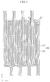
- FIG. 4 shows an enlarged view of connection wires in region A of FIG. 1 .
- the first and second connection wires 311 and 312 include a section extended to the display panel 100 from the pad (P) in a second direction, in which these connection wires are extended to the display panel 100 in a forward direction, bent to extend toward the pad (P) in a backward direction, and then bent to extend to the display panel 100.
- An X axis represents the first direction and a Y axis indicates the second direction.
- the first and second connection wires 311 and 312 are bent at least twice, and these wires are bent toward backward direction at least once.
- the substrate (SUB) is divided into a display area (DA) for displaying an image and a peripheral area (PA) neighboring the display area (DA).
- a display panel 100 for emitting light may be provided in the display area (DA).
- a plurality of connection wires 300, a pad (P), and a flexible film 400 for driving the display panel 100 may be provided in the peripheral area (PA).
- the display panel 100 formed in the display area (DA) of the substrate (SUB), includes first gate wires (GW1), second gate wires (GW2), data wires (DW), a display unit 140, and a pixel 150.
- the gate driver 210 In response to a control signal supplied by an external control circuit (e.g., a timing controller), the gate driver 210 sequentially supplies scan signals to first scan lines (SC2-SC2n) or second scan lines (SC1-SC2n-1) included in the first gate wires GW1 or the second gate wires GW2.
- the pixel 150 is selected by the scan signal and sequentially receives a data signal.
- the gate driver 210 shown in FIG. 2 is formed in a first driving chip 200 on a flexible film 400, and it is shown in FIG. 2 for convenience of description.
- the first gate wires GW1 as shown in FIG. 3 are provided on the substrate (SUB) with a first insulating layer GI1 therebetween, and are extended in a first direction.
- the first gate wires GW1 include a second scan line (SC2n-1) and emission control line (E1-En).
- the second scan line (SC2n-1) is connected to a gate driver 210 and receives a scan signal from the gate driver 210.
- An emission control line (En) is connected to an emission control driver 220 and receives an emission control signal from the emission control driver 220.
- the emission control driver 220 shown in FIG. 2 is formed in the first driving chip 200 on the flexible film 400 and is shown in FIG. 2 for ease of description.
- the second gate wires GW2 are provided on the first gate wires GW1 with a second insulating layer GI2 therebetween, and are extended in the first direction.
- the second gate wires GW2 include a first scan line (SC2n) and an initialization power line (Vinit).
- the first gate wires GW1 do not overlap the second gate wires GW2.
- the first scan line (SC2n) is connected to the gate driver 210 and receives a scan signal from the gate driver 210.
- the initialization power line (Vinit) is connected to the gate driver 210 and receives initialization power from the gate driver 210.
- the initialization power line (Vinit) receives the initialization power from the gate driver 210, and it may be connected to another additional component and may receive initialization power from the additional component.
- the emission control driver 220 sequentially supplies an emission control signal to the emission control line (En) corresponding to a control signal supplied by an external component such as a timing controller.
- the pixel 150 undergoes emission control by the emission control signal. That is, the emission control signal controls an emission time of the pixel 150.
- the emission control driver 220 may be omitted depending on a configuration of the pixel 150.
- the data driver 230 supplies a data signal to a data line (DAm) from among the data wires (DW) corresponding to a control signal supplied by an external component such as a timing controller.
- the data signal provided to the data line (DAm) is supplied to the pixel 150 selected by a scan signal each time when the scan signal is supplied to the first scan line (SC2n) or the second scan line (SC2n-1).
- the pixel 150 charges a voltage corresponding to the data signal and emits light with a corresponding luminance.
- the data driver 230 shown in FIG. 2 is formed in the first driving chip 200 on the flexible film 400, and is shown in FIG. 2 for convenience of description.
- the data wires (DW) are provided on the second gate wires GW2 with a third insulating layer (ILD) therebetween, and are extended in the second direction crossing the first direction.
- the data wires (DW) include data lines (DA1-DAm) and a driving power line (ELVDDL).
- the data line (DAm) is connected to the data driver 230 and receives a data signal from the data driver 230.
- the driving power line (ELVDDL) is connected to a first power source (ELVDD) and receives driving power from the first power source (ELVDD).
- the driving power line (ELVDDL) and the data line (DAm) may be formed on the same layer on the third insulating layer (ILD).
- the driving power line (ELVDDL) and the data line (DAm) may also be formed on different layers.
- the driving power line (ELVDDL) may be formed on the same layer as the first gate wire GW1
- the data line (DAm) may be formed on the same layer as the second gate wire GW2.
- the driving power line (ELVDDL) may be formed on the same layer as the second gate wire GW2
- the data line (DAm) may be formed on the same layer as the first gate wire GW1
- the display unit 140 includes a plurality of pixels 150 provided in crossing regions of the first gate wires GW1, the second gate wires GW2, and the data wires (DW).
- the pixel 150 includes an organic light emitting element for emitting light with luminance corresponding to a driving current that corresponds to the data signal, and a pixel circuit for controlling the driving current flowing to the organic light emitting element.
- the pixel circuit is connected to the first gate wires GW1, the second gate wires GW2, and the data wires (DW), and the organic light emitting element is connected to the pixel circuit.
- the pixel 150 is not limited to contain the organic light emitting element, for example, it may contain a liquid crystal display element or an electrophoretic display element.
- the organic light emitting element of the display unit 140 is connected to an external first power source (ELVDD) with a pixel circuit therebetween, and a second power source (ELVSS).
- the first power source (ELVDD) and the second power source (ELVSS) supply driving power and common power respectively to the pixel 150 of the display unit 140, and the pixel 150 responds to the data signal according to the driving power and the common power provided to the pixel 150 by emitting light with luminance corresponding to the driving current passing through the organic light emitting element from the first power source (ELVDD).
- the gate wires that traverse the pixel 150 in the first direction and do not overlap each other that is, the first gate wires GW1 including a second scan line (SC2n-1) and an emission control line (En) and the second gate wires GW2 including a first scan line (SC2n) and an initialization power line (Vinit) are not provided on the same layer, but the gate wires that are the first gate wires GW1 and the second gate wires GW2 are provided on different layers with a second insulating layer GI2 therebetween so that the distance (W) between the neighboring gate wires provided on the different layers may be formed to be narrow and more pixels 150 may be formed in the same area.
- a high-resolution display device may be formed.
- connection wires 300 connect a plurality of signal lines, including a data line (DAm) and a scan line (SCn) of the display panel 100 to the pad (P).
- the connection wires 300 correspond to the fan out unit in the display device for connecting the gate line or the data line to the gate IC or the data IC.
- part of a plurality of connection wires 300 includes a section extended to the display panel 100 from the pad (P) in the second direction, in which these connection wires are extended to the display panel 100 in a forward direction, bent and extended toward the pad (P) in a backward direction, and then bent and extended to the display panel 100, so as to increase resistance of the connection wires.
- the plurality of connection wires 300 are bent at least twice, and these wires are bent toward backward direction at least once.
- the connection wires may include a section formed by rotating the letter S by 90 degrees.
- connection wires 300 connected to the display panel 100 are divided and connected to the connecting pad terminals P1 and P3 of two regions. That is, some of the connection wires are connected to the connecting pad terminal P1 and the rest of the connection wires are connected to the connecting pad terminal P3.
- a dummy pad terminal P2 may be provided between the connecting pad terminals P1 and P3. That is, no connection wire is connected to the dummy pad terminal P2.
- a region through which a portable terminal, for example a camera module for a smartphone or a tablet PC passes, may be provided in a region through which the connection wire 300 passes. That is, the camera module may pass through a hole (H) of FIG. 1 .
- the connection wire is not connected to the dummy pad terminal P2. Accordingly, the hole is provided between the connection wires 311 and 313, which neighbor each other, and lengths of the connection wires 311 and 313 become different.
- resistance values are different from each other, thus signals may not simultaneously reach the display panel 100.
- part of a plurality of connection wires 300 includes a section extended to the display panel 100 from the pad (P) in the second direction, in which the connection wires 300 are extended to the display panel 100 in a forward direction, bent and extended toward the pad (P) in a backward direction, and then bent and extended to the display panel 100.
- the connection wires 300 are bent at least twice, and these wires are bent toward backward direction at least once.
- the neighboring first and second connection wires 311 and 312 from among a plurality of connection wires 300 respectively include first connectors 311 a and 312a, second connectors 311b and 312b, and extensions 311c and 312c.
- the first connection wire 311 includes a first connector 311a, a second connector 311 b, and an extension 311 c.
- the first connector 311 a is connected to a pad (P).
- the first connector 311 a is extended and formed in the second direction. That is, the first connector 311a is formed to extend to the display panel 100 from the pad (P). As shown in FIG. 1 and FIG. 5 , the first connector 311a may be formed in a linear manner in the second direction.
- the second connector 311b is connected to the display panel 100 and is connected to the first connector 311a through the extension 311c.
- the second connector 311 b is formed to be bent and then connected to a signal line of the display panel 100.
- the extension 311c is connected between the first and second connectors 311 a and 311 b to increase resistance of the first connection wire 311.
- the extension 311 c increases the length of the connection wire to increase resistance of the wire.
- the extension 311 c corresponds to the section formed by rotating the letter S by 90 degrees.
- the extension 311c includes a plurality of first bridges (311c-1, 311c-3, 311c-5) and a plurality of second bridges (311c-2, 311c-4).
- the first bridges (311c-1, 311c-3, and 311c-5) are disposed parallel to the first connector 311a
- the second bridges (311c-2 and 311c-4) are disposed to be vertical to the first bridges (311c-1, 311c-3, and 311c-5).
- the plurality of second bridges may form a predetermined angle with the first bridges, in which the predetermined angle is 90 degrees or not 90 degrees. For example, one first bridge may form an angle smaller than 90 degrees with one second bridge, then this second bridge may form an angle larger than 90 degrees with the next first bridge.
- the first bridges (311c-1, 311c-3, and 311c-5) and the second bridges (311c-2, 311c-4) are alternately connected to each other.
- the extension 311c may be disposed in a like manner as the letter S is rotated by 90 degrees. That is, the first bridge (311c-1), the second bridge (311c-2), the first bridge (311c-3), the second bridge (311c-4), and the first bridge (311c-5) are sequentially disposed so that they may be disposed according to the above-noted shape.
- the first bridge (311c-1) is connected to the first connector 311a, and is disposed along the same direction as the first connector 311a.
- the first connection wire 311 is extended to the display panel 100 from the pad (P) and a section going backward is formed in the extension 311c.
- the backward section represents a section extended to the display panel 100 from the pad (P) in the second direction on the first connection wire 311, in which the connection wire 311 is extended to the display panel 100 in a forward direction, bent and extended toward the pad (P) in a backward direction in the backward section, and then bent and extended to the display panel 100.
- the connection wire 311 is bent at least twice, and the wire is bent toward backward direction at least once.
- the first bridges (311c-1, 311c-3, and 311c-5) are disposed parallel to each other. That is, the first bridges (311c-1, 311c-3, and 311c-5) are disposed parallel to the first connector 311a.
- the neighboring first bridges (311c-3 and 311 c- 5) may be formed to have the same length.
- the second bridges (311c-2 and 311c-4) are disposed parallel to each other. That is, the second bridges (311c-2 and 311c-4) are disposed parallel to be vertical to the first connector 311a.
- the second bridges (311c-2 and 311c-4) may be formed to have different lengths.
- the second connection wire 312 includes a first connector 312a, a second connector 312b, and an extension 312c.
- the first connector 312a is connected to the pad (P) in a like manner as the first connector 311a of the first connection wire 311.
- the first connector 312a is extended in the second direction. That is, the first connector 312a is extended to the display panel 100 from the pad (P).
- the first connector 312a may be formed in a linear manner in the second direction.
- the second connector 312b is connected to the display panel 100 and is connected to the first connector 312a through the extension 312c.
- the second connector 312b may be bent and be connected to the signal line of the display panel 100.
- the extension 312c is connected between the first and second connectors 312a and 312b and may increase resistance of the second connection wire 312.
- the extension 312c increases the length of the connection wire to increase resistance of the wire.
- the extension 312c is formed with a section configured by rotating the letter S by 90 degrees.
- the extension 312c includes a plurality of first bridges (312c-1, 312c-3, and 312c-5) and a plurality of second bridges (312c-2 and 312c-4).
- the first bridges (312c-1, 312c-3, and 312c-5) are disposed parallel to the first connector 312a
- the second bridges (312c-2 and 312c-4) are disposed to be vertical to the first bridges (312c-1, 312c- 3, and 312c- 5).
- the length (e.g., L1) of the first bridges (312c-1, 312c-3, and 312c-5) is formed to be greater than the length (e.g., M1) of the second bridges (312c-2 and 312c-4).
- the plurality of second bridges may form a predetermined angle with the first bridges, in which the predetermined angle is 90 degrees or not 90 degrees.
- the predetermined angle is 90 degrees or not 90 degrees.
- one first bridge may form an angle smaller than 90 degrees with one second bridge, then this second bridge may form an angle larger than 90 degrees with the next first bridge.
- the first bridges (312c-1, 312c-3, and 312c-5) and the second bridges (312c-2 and 312c-4) are alternately connected.
- the extension 312c may be disposed in a shape formed by rotating the letter S by 90 degrees. That is, the first bridge (312c-1), the second bridge (312c- 2), the first bridge (312c- 3), the second bridge (312c- 4), and the first bridge (312c- 5) are sequentially arranged so they may be disposed according to the above-noted shape.
- the first bridge (312c-1) is connected to the first connector 312a and is disposed along the same direction as the first connector 312a.
- the second connection wire 312 has a section extending to the display panel 100 from the pad (P) and going backward in the extension 312c.
- the backward section represents a section extended to the display panel 100 from the pad (P) in the second direction on the second connection wire 312, in which the connection wire 312 is extended to the display panel 100 in a forward direction, bent and extended toward the pad (P) in a backward direction in the backward section, and the bent and extended to the display panel 100.
- the connection wire 312 is bent at least twice, and the wire is bent toward backward direction at least once.
- the extension 311c of the first connection wire 311 and the extension 312c of the second connection wire 312 may be formed to be rotated by 180 degrees and to be symmetrical with each other.
- the extension 311 c of the first connection wire 311 is rotated by 180 degrees with respect to a virtual line (11) passing through the centers of the extension 311 c and 312c in the first direction, it may become the same shape as the extension 312c of the second connection wire 312.
- the neighboring first and second connection wires 311 and 312 from among a plurality of connection wires 300 are separated and disposed with a predetermined gap D1 to form the above-noted shape. That is, as shown in FIG. 4 and FIG. 6 , the two first and second connection wires 311 and 312 are extended and formed with a constant gap D1 therebetween.
- the first bridges (311c-1, 311c-3, and 311c-5) of the neighboring first connection wire 311 are disposed separately from the second bridges (312c-1, 312c- 3, and 312c- 5) of the second connection wire 312 with a constant gap D1.
- the second bridges (311c-2 and 311c-4) of the neighboring first connection wire 311 are disposed separately from the second bridges (312c-2 and 312c-4) of the second connection wire 312 with the constant gap D1.
- the first and second connection wires 311 and 312 include the section going backward in the second direction.
- the first and second connection wires 311 and 312 include the section going backward in the second direction so resistance of the connection wire may be increased without deteriorating integrity of the connection wire.
- first and second connection wires 311 and 312 are formed on different layers.
- the first connection wire 311 and the second connection wire 312 are sequentially stacked on the substrate (SUB).
- An insulating layer IL2 may be provided between the first and second connection wires 311 and 312.
- the first connection wire 311 may be formed on the same layer as the first gate wire GW1 of the display panel 100.
- the second connection wire 312 may be formed on the same layer as the second gate wire GW2 of the display panel 100.
- the gap D1 between the first and second connection wires 311 and 312 may be minimized by forming the first and second connection wires 311 and 312 on different layers. That is, when the gap D1 between the first and second connection wires 311 and 312 is reduced, the possibility of short-circuiting the first and second connection wires 311 and 312 is reduced.
- FIG. 13 shows a comparison of connection wires configured with a single layer and double layers.
- FIG. 13 (A) when the first and second connection wires 311 and 312 are formed with the constant gap D1, an insulating layer is provided between the first and second connection wires 311 and 312, thus the possibility of short circuiting the first and second connection wires 311 and 312 by a foreign particle (E) is low.
- FIG. 13 (B) when the first and second connection wires 311 and 312 are formed on the same layer with the same gap D1 shown in FIG. 13 (A) , the possibility of short circuiting the first and second connection wires 311 and 312 by a foreign particle (E) is increased.
- the first and second connection wires 311 and 312 are formed on different layers to prevent the first and second connection wires 311 and 312 from being short-circuited by a foreign particle.
- the gap D1 between the first and second connection wires 311 and 312 may be minimized so that the integrity of the connection wire may be increased.
- the width S1 of the first connection wire 311 may correspond to the width S2 of the second connection wire 312.
- first and second connection wires 311 and 312 are formed as double layers, and they may be configured to be triple or quadruple layers.
- the pad (P) is configured with a plurality of connecting pad terminals P1 and P3 and a plurality of dummy pad terminals P2.
- a plurality of connecting pad terminals P1 and P3 may be connected to a plurality of connection wires 300. That is, some of the connection wires are connected to the connecting pad terminal P1 and the rest of the connection wires are connected to the connecting pad terminal P3.
- a dummy pad terminal P2 may be provided between the connecting pad terminals P1 and P3.
- the connection wire is not connected to the dummy pad terminal P2.
- the flexible film 400 is connected to the pad (P) in the peripheral area (PA).
- a first driving chip 200 for driving the display panel 100 may be mounted on the flexible film 400.
- the flexible film 400 may be a chip on film (COF).
- the flexible film 400 may be generated by forming a plurality of metal wires on a flexible base film.
- the first driving chip 200 may be installed on the base film and may generate a driving signal.
- the first driving chip 200 may be a scan driving circuit for receiving a control signal and generating a scan signal or a data driving circuit for generating a data signal. That is, the gate driver 210 or the data driver 230 may be formed in the first driving chip 200.
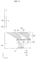
- the COF type flexible film 400 is disposed on the pad (P), moreover, as shown in FIG. 9 , a chip on glass type second driving chip 500 may be disposed in the peripheral area (PA) of the substrate (SUB). A first side of the second driving chip 500 is connected to the pad (P). A second side of the second driving chip 500 may be connected to another pad (N) by an additional wire formed in the peripheral area (PA).
- the second driving chip 500 may be a scan driving circuit for receiving a control signal and generating a scan signal or a data driving circuit for generating a data signal. That is, the gate driver 210 or the data driver 230 may be formed in the second driving chip 500.
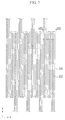
- connection wire In a variation of the connection wire according to the first embodiment of the inventive concept, the first and second connection wires 331 and 332 are disposed such that their neighboring edges may overlap each other.
- first and second connection wires 311 and 312 are separately disposed with the constant gap D1 in FIG. 4 to FIG. 6 , and they may be disposed such that the gap D1 may be close to 0 in the variation shown in FIG. 7 and FIG. 8 .
- connection wires 300 may be further improved. That is, the connection wires 300 may be more densely disposed by removing the gap among the connection wires 300.
- a display device including connection wires according to a second embodiment of the inventive concept will now be described with reference to FIG. 10 to FIG. 12 .
- the same detailed descriptions as the first embodiment of the inventive concept will be omitted in the second embodiment of the inventive concept.
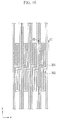
- FIG. 10 shows an enlarged view of a connection wire according to the second embodiment of the inventive concept
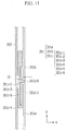
- FIG. 11 shows first and second connection wires of FIG. 10
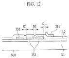
- FIG. 12 shows a cross-sectional view with respect to line XII-XII of FIG. 10 .
- the neighboring first and second connection wires 351 and 352 from among a plurality of connection wires 300 include a section extended to the display panel 100 from the pad (P) in the second direction, in which the connection wires 351 and 352 are extended to the display panel 100 in a forward direction, bent and extended toward the pad (P) in a backward direction, and then bent and extended to the display panel 100 so as to increase the resistance of the connection wires.
- the connection wires 351 and 352 are bent at least twice, and these wires are bent toward backward direction at least once.
- the connection wires may include a section formed by rotating the letter S by 90 degrees.
- the extension 351c of the first connection wire 351 and the extension 352c of the second connection wire 352 may be formed to be rotated by 180 degrees and to be symmetrical with each other.
- the extension 351 c of the first connection wire 351 is rotated by 180 degrees with respect to a virtual line (l2) passing between the extension 351 c of the first connection wire 351 and the extension 352c of the second connection wire 352 in the first direction, it may become the same shape as the extension 352c of the second connection wire 352.
- the first connection wire 351 includes a first connector 351 a, a second connector 351b, and an extension 351 c.
- the first connector 351 a is connected to the pad (P).
- the first connector 351 a is extended and formed in the second direction. That is, the first connector 351 a is formed to extend to the display panel 100 from the pad (P).
- the first connector 351 a may be formed in a linear manner in the second direction.
- the second connector 351 b is connected to the display panel 100 and is connected to the first connector 351 a through the extension 351 c.
- the second connector 351 b is formed to be bent and then connected to a signal line of the display panel 100.
- the extension 351 c is connected between the first and second connectors 351 a and 351 b to increase resistance of the first connection wire 351.
- the extension 351 c increases the length of the connection wire to increase resistance of the wire.
- the extension 351 c may include a section formed by rotating the letter S by 90 degrees so as to increase the length of the connection wire.
- the extension 351 c includes a plurality of first bridges (351 c- 1, 351c-3, and 351 c- 5) and a plurality of second bridges (351c-2, 351c-4, and 351 c- 6).
- the first bridges (351c-1, 351c-3, and 351c-5) are disposed parallel to the first connector 351a
- the second bridges (351c-2, 351c-4, and 351c-6) are disposed to be vertical to the first bridges (351c-1, 351c-3, and 351c-5).
- the second bridges (351c-2 and 351c-4) may be formed to have the same length.
- the plurality of second bridges may form a predetermined angle with the first bridges, in which the predetermined angle is 90 degrees or not 90 degrees.
- the predetermined angle is 90 degrees or not 90 degrees.
- one first bridge may form an angle smaller than 90 degrees with one second bridge, then this second bridge may form an angle larger than 90 degrees with the next first bridge.
- the first bridges (351c-1, 351c-3, and 351c-5) and the second bridges (351c-2, 351c-4, and 351c-6) are alternately connected to each other.
- the extension 351 c may be disposed in a like manner as the letter S is rotated by 90 degrees.
- first bridge (351c-1), the second bridge (351c-2), the first bridge (351c-3), the second bridge (351c-4), the first bridge (351c-5), and the second bridge (351c-6) are sequentially disposed so they may be disposed according to the above-noted shape.
- the first bridge of the neighboring second connection wire 352 is not provided among the first bridges (351c-1, 351c-3, and 351c-5) of the first connection wire 351. That is, the extensions of the first and second connection wires 311 and 312 overlap each other in the first embodiment of the inventive concept, and the extensions of the first and second connection wires 351 and 352 are disposed separately from each other in the second embodiment of the inventive concept.
- the first and second connection wires 351 and 352 are formed on different layers.
- the first connection wire 351 and the second connection wire 352 are sequentially stacked on the substrate (SUB).
- An insulating layer IL2 may be provided between the first and second connection wires 351 and 352.
- the first and second connection wires 311 and 312 are formed on different layers to prevent the first and second connection wires 311 and 312 from being short-circuited by a foreign particle, and the gap between the neighboring first and second connection wires 311 and 312 may be minimized to increase the integrity of the connection wires.
Landscapes
- Physics & Mathematics (AREA)
- Engineering & Computer Science (AREA)
- Nonlinear Science (AREA)
- General Physics & Mathematics (AREA)
- Chemical & Material Sciences (AREA)
- Crystallography & Structural Chemistry (AREA)
- Microelectronics & Electronic Packaging (AREA)
- Optics & Photonics (AREA)
- Mathematical Physics (AREA)
- Theoretical Computer Science (AREA)
- Computer Hardware Design (AREA)
- Devices For Indicating Variable Information By Combining Individual Elements (AREA)
- Electroluminescent Light Sources (AREA)
- Vehicle Body Suspensions (AREA)
- Diaphragms For Electromechanical Transducers (AREA)
- Measuring Pulse, Heart Rate, Blood Pressure Or Blood Flow (AREA)
Abstract

Description
- The present invention relates to a display device.
- Currently known display devices include a liquid crystal display (LCD), a plasma display panel (PDP), an organic light emitting diode (OLED) device, a field effect display (FED), and an electrophoretic display device.
- In particular, the OLED device of the above known display devices includes two electrodes and an organic emission layer positioned between the two electrodes; an electron injected from one electrode and a hole injected from the other electrode are coupled with each other in the organic emission layer to generate an exciton; and the exciton emits energy to emit light.
- Since the OLED device has a self-luminance characteristic and does not require a separate light source, unlike an LCD, its thickness and weight may be reduced. Further, since the OLED device has superior characteristics, such as low power consumption, high luminance, and a high response speed, the OLED device has gained attention as a next-generation display device.
- To drive an organic light emitting element of the organic light emitting device, a fan out unit for connecting a gate line (or a data line) and a gate IC (or a data IC) is formed in a peripheral area of a substrate. However, connection wires formed on the fan out unit may have different lengths so as to have different resistances, thereby delaying signals transmitted through the connection wires.
- The present invention has been made to provide a display device for minimizing differences in the length of connection wires of a fan out unit.
- According to an embodiment of the present invention, there is provided a display device including: a substrate including a display area for displaying an image and a peripheral area neighboring the display area; a plurality of signal lines formed in the display area; a pad formed in the peripheral area; and a plurality of connection wires for connecting the signal lines and the pad, wherein a first connection wire and a second connection wire neighboring the first connection wire from among the plurality of connection wires are disposed on different layers, and the first connection wire and the second connection wire are disposed in the peripheral area in a shape so that they extend to the display area from the pad and bend at least twice to have at least one being bent toward backward direction.
- The first and second connection wires may be disposed separately from each other with a predetermined gap.
- The first connection wire and the second connection wire each may include: a first connector connected to the pad and a second connector connected to the signal line; and an extension connected between the first and second connectors, the extension including a plurality of first bridges disposed parallel to the first connector and a plurality of second bridges forming a predetermined angle with the first bridges, and the first bridges and the second bridges being alternately connected.
- The adjacent first and second bridges may be vertical to each other.
- The first bridges may be disposed parallel to each other.
- The neighboring first bridges from among the first bridges may be formed to have the same length.
- The second bridges may be disposed parallel to each other.
- The second bridges may be formed to have different lengths.
- The second bridges may be formed to have the same length.
- The first bridges may be longer than the second bridges.
- The second connector may be bent.
- Extension of the first connection wire and extension of the second connection wire neighboring the first connection wire may be rotated by 180 degrees and may be symmetrical with each other.
- Neighboring edges of the first and second connection wires may overlap each other.
- The pad may include a plurality of connecting pad terminals connected to the connection wires and a plurality of dummy pad terminals not connected to the connection wires.
- The first and second connection wires may be connected to the connecting pad terminal.
- The display device may further include a flexible film that is connected to the pad and that includes a first side on which a first driving chip is provided.
- The display device may further include a second driving chip formed in the peripheral area and connected to the pad.
- An insulating layer may be provided between the first and second connection wires.
- Signal lines connected to the first and second connection wires from among the signal lines may be formed on different layers.
- The connection wires may be formed to be double layers, triple layers, or quadruple layers.
- The signal lines may be gate lines.
- The signal lines may be data lines.
- In an embodiment of the present invention, there is provided a display device including: a substrate having a display panel and a pad; a plurality of signal lines formed in the display panel; a plurality of connecting pad terminals formed in the pad; and a plurality of connection wires formed on the substrate for connecting the signal lines and the connecting pad terminals, wherein a first connection wire and a second connection wire neighboring the first connection wire from among the plurality of connection wires are disposed and separated from each other with a predetermined gap on different layers, and the first connection wire and the second connection wire having a same length, which are shaped to extend to the display panel from the pad and are bent at least twice to have at least one being bent toward backward direction.
- At least some of the above and other features of the invention are set out in the claims.
- In the display device according to an embodiment of the present invention, the transmission of signals is prevented from being delayed by allowing the connection wires of the fan out unit to have the same length.
- Further, adjacent connection wires are disposed on different layers to minimize the gap among the connection wires and thereby increase the integrity of the connection wires.
- In addition, adjacent connection wires are disposed on different layers to prevent the connection wires from being short-circuited by a foreign particle.
- The invention may best be understood from the following detailed description of embodiments thereof, taken in conjunction with the appended drawings, and in which:
-
FIG. 1 shows a partial top plan view of a display device including connection wires according to a first embodiment of the inventive concept; -
FIG. 2 shows a display area ofFIG. 1 according to an embodiment of the inventive concept; -
FIG. 3 shows a cross-sectional view with respect to line III-III ofFIG. 2 according to an embodiment of the inventive concept; -
FIG. 4 shows an enlarged view of connection wires in region A ofFIG. 1 according to a first embodiment of the inventive concept; -
FIG. 5 shows first and second connection wires ofFIG. 4 according to an embodiment of the inventive concept; -
FIG. 6 shows a cross-sectional view with respect to line VI-VI ofFIG. 4 according to an embodiment of the inventive concept; -
FIG. 7 shows an exemplary variation of connection wires according to a first embodiment of the inventive concept; -
FIG. 8 shows a cross-sectional view with respect to line VIII-VIII ofFIG. 7 according to an embodiment of the inventive concept; -
FIG. 9 shows an exemplary variation of a driving chip ofFIG. 1 according to an embodiment of the inventive concept; -
FIG. 10 shows an enlarged view of connection wires according to a second embodiment of the inventive concept; -
FIG. 11 shows first and second connection wires ofFIG. 10 according to an embodiment of the inventive concept; -
FIG. 12 shows a cross-sectional view with respect to line XII-XII ofFIG. 10 according to an embodiment of the inventive concept; and -
FIG. 13 shows a comparison of connection wires configured with a single layer and double layers according to an embodiment of the inventive concept. - Since the drawings in
FIGS. 1-13 are intended for illustrative purpose, the elements in the drawings are not necessarily drawn to scale. For example, some of the elements may be enlarged or exaggerated for clarity purpose. - In the following detailed description, only certain embodiments of the inventive concept have been shown and described, simply by way of illustration. As those skilled in the art would realize, the described embodiments may be modified in various different ways, all without departing from the scope of the invention. The drawings and description are to be regarded as illustrative in nature and not restrictive. Like reference numerals designate like elements throughout the specification.
- The size and thickness of each component illustrated in the drawings are arbitrarily illustrated in the drawings for better understanding and ease of description, but the present invention is not limited to the illustrations.
- It will be understood that when an element, for example, a layer, film, region, or substrate is referred to as being "on" another element, it can be directly on the other element or intervening elements may also be present. In addition, throughout the specification, unless explicitly described to the contrary, the word "comprise" and variations, for example, "comprises" or "comprising" will be understood to imply the inclusion of stated elements but not the exclusion of any other elements. It is understood that the term "on" and similar terms are used generally and are not necessarily related to a gravitational reference.
- A display device including connection wires according to a first embodiment of the inventive concept will now be described with reference to
FIG. 1 to FIG. 6 . -
FIG. 1 shows a partial top plan view of a display device including connection wires according to a first embodiment of the inventive concept,FIG. 2 shows a display area ofFIG. 1 , andFIG. 3 shows a cross-sectional view with respect to line III-III ofFIG. 2 . - Referring to
FIG. 1 to FIG. 3 , the display device includes a substrate (SUB), adisplay panel 100, a pad (P), aflexible film 400, and a plurality ofconnection wires 300. - From among a plurality of
connection wires 300 for connecting thedisplay panel 100 and the pad (P), first andsecond connection wires FIG. 4 shows an enlarged view of connection wires in region A ofFIG. 1 . As shown inFIG. 4 , the first andsecond connection wires display panel 100 from the pad (P) in a second direction, in which these connection wires are extended to thedisplay panel 100 in a forward direction, bent to extend toward the pad (P) in a backward direction, and then bent to extend to thedisplay panel 100. An X axis represents the first direction and a Y axis indicates the second direction. The first andsecond connection wires - Referring to
FIG. 1 , the substrate (SUB) is divided into a display area (DA) for displaying an image and a peripheral area (PA) neighboring the display area (DA). Adisplay panel 100 for emitting light may be provided in the display area (DA). A plurality ofconnection wires 300, a pad (P), and aflexible film 400 for driving thedisplay panel 100 may be provided in the peripheral area (PA). The above-described components provided on the substrate (SUB) will be described further. - Referring to
FIG. 2 andFIG. 3 , thedisplay panel 100 formed in the display area (DA) of the substrate (SUB), includes first gate wires (GW1), second gate wires (GW2), data wires (DW), adisplay unit 140, and apixel 150. - In response to a control signal supplied by an external control circuit (e.g., a timing controller), the
gate driver 210 sequentially supplies scan signals to first scan lines (SC2-SC2n) or second scan lines (SC1-SC2n-1) included in the first gate wires GW1 or the second gate wires GW2. Thepixel 150 is selected by the scan signal and sequentially receives a data signal. Thegate driver 210 shown inFIG. 2 is formed in afirst driving chip 200 on aflexible film 400, and it is shown inFIG. 2 for convenience of description. - The first gate wires GW1 as shown in
FIG. 3 are provided on the substrate (SUB) with a first insulating layer GI1 therebetween, and are extended in a first direction. The first gate wires GW1 include a second scan line (SC2n-1) and emission control line (E1-En). The second scan line (SC2n-1) is connected to agate driver 210 and receives a scan signal from thegate driver 210. An emission control line (En) is connected to anemission control driver 220 and receives an emission control signal from theemission control driver 220. In a like manner as thegate driver 210, theemission control driver 220 shown inFIG. 2 is formed in thefirst driving chip 200 on theflexible film 400 and is shown inFIG. 2 for ease of description. - The second gate wires GW2 are provided on the first gate wires GW1 with a second insulating layer GI2 therebetween, and are extended in the first direction. The second gate wires GW2 include a first scan line (SC2n) and an initialization power line (Vinit). The first gate wires GW1 do not overlap the second gate wires GW2.
- The first scan line (SC2n) is connected to the
gate driver 210 and receives a scan signal from thegate driver 210. The initialization power line (Vinit) is connected to thegate driver 210 and receives initialization power from thegate driver 210. - In an embodiment of the inventive concept, the initialization power line (Vinit) receives the initialization power from the
gate driver 210, and it may be connected to another additional component and may receive initialization power from the additional component. - The
emission control driver 220 sequentially supplies an emission control signal to the emission control line (En) corresponding to a control signal supplied by an external component such as a timing controller. Thepixel 150 undergoes emission control by the emission control signal. That is, the emission control signal controls an emission time of thepixel 150. Theemission control driver 220 may be omitted depending on a configuration of thepixel 150. - The
data driver 230 supplies a data signal to a data line (DAm) from among the data wires (DW) corresponding to a control signal supplied by an external component such as a timing controller. The data signal provided to the data line (DAm) is supplied to thepixel 150 selected by a scan signal each time when the scan signal is supplied to the first scan line (SC2n) or the second scan line (SC2n-1). Thepixel 150 charges a voltage corresponding to the data signal and emits light with a corresponding luminance. In a like manner as thegate driver 210, thedata driver 230 shown inFIG. 2 is formed in thefirst driving chip 200 on theflexible film 400, and is shown inFIG. 2 for convenience of description. - The data wires (DW) are provided on the second gate wires GW2 with a third insulating layer (ILD) therebetween, and are extended in the second direction crossing the first direction. The data wires (DW) include data lines (DA1-DAm) and a driving power line (ELVDDL). The data line (DAm) is connected to the
data driver 230 and receives a data signal from thedata driver 230. The driving power line (ELVDDL) is connected to a first power source (ELVDD) and receives driving power from the first power source (ELVDD). - The driving power line (ELVDDL) and the data line (DAm) may be formed on the same layer on the third insulating layer (ILD). The driving power line (ELVDDL) and the data line (DAm) may also be formed on different layers. For example, the driving power line (ELVDDL) may be formed on the same layer as the first gate wire GW1, and the data line (DAm) may be formed on the same layer as the second gate wire GW2. On the contrary, the driving power line (ELVDDL) may be formed on the same layer as the second gate wire GW2, the data line (DAm) may be formed on the same layer as the first gate wire GW1, and the
display unit 140 includes a plurality ofpixels 150 provided in crossing regions of the first gate wires GW1, the second gate wires GW2, and the data wires (DW). Thepixel 150 includes an organic light emitting element for emitting light with luminance corresponding to a driving current that corresponds to the data signal, and a pixel circuit for controlling the driving current flowing to the organic light emitting element. The pixel circuit is connected to the first gate wires GW1, the second gate wires GW2, and the data wires (DW), and the organic light emitting element is connected to the pixel circuit. Thepixel 150 is not limited to contain the organic light emitting element, for example, it may contain a liquid crystal display element or an electrophoretic display element. - The organic light emitting element of the
display unit 140 is connected to an external first power source (ELVDD) with a pixel circuit therebetween, and a second power source (ELVSS). The first power source (ELVDD) and the second power source (ELVSS) supply driving power and common power respectively to thepixel 150 of thedisplay unit 140, and thepixel 150 responds to the data signal according to the driving power and the common power provided to thepixel 150 by emitting light with luminance corresponding to the driving current passing through the organic light emitting element from the first power source (ELVDD). - According to an embodiment of the inventive concept, the gate wires that traverse the
pixel 150 in the first direction and do not overlap each other, that is, the first gate wires GW1 including a second scan line (SC2n-1) and an emission control line (En) and the second gate wires GW2 including a first scan line (SC2n) and an initialization power line (Vinit) are not provided on the same layer, but the gate wires that are the first gate wires GW1 and the second gate wires GW2 are provided on different layers with a second insulating layer GI2 therebetween so that the distance (W) between the neighboring gate wires provided on the different layers may be formed to be narrow andmore pixels 150 may be formed in the same area. Thus, a high-resolution display device may be formed. - Referring to
FIG. 1 andFIG. 2 , a plurality ofconnection wires 300 connect a plurality of signal lines, including a data line (DAm) and a scan line (SCn) of thedisplay panel 100 to the pad (P). Here, theconnection wires 300 correspond to the fan out unit in the display device for connecting the gate line or the data line to the gate IC or the data IC. - According to the first embodiment of the inventive concept, part of a plurality of
connection wires 300 includes a section extended to thedisplay panel 100 from the pad (P) in the second direction, in which these connection wires are extended to thedisplay panel 100 in a forward direction, bent and extended toward the pad (P) in a backward direction, and then bent and extended to thedisplay panel 100, so as to increase resistance of the connection wires. The plurality ofconnection wires 300 are bent at least twice, and these wires are bent toward backward direction at least once. For example, the connection wires may include a section formed by rotating the letter S by 90 degrees. - As shown in
FIG. 1 , a plurality ofconnection wires 300 connected to thedisplay panel 100 are divided and connected to the connecting pad terminals P1 and P3 of two regions. That is, some of the connection wires are connected to the connecting pad terminal P1 and the rest of the connection wires are connected to the connecting pad terminal P3. A dummy pad terminal P2 may be provided between the connecting pad terminals P1 and P3. That is, no connection wire is connected to the dummy pad terminal P2. - A region through which a portable terminal, for example a camera module for a smartphone or a tablet PC passes, may be provided in a region through which the
connection wire 300 passes. That is, the camera module may pass through a hole (H) ofFIG. 1 . As such, the connection wire is not connected to the dummy pad terminal P2. Accordingly, the hole is provided between theconnection wires connection wires connection wires display panel 100. - In the first embodiment of the inventive concept, to solve the above problem, for the purpose of increasing resistance of the short connection wire, part of a plurality of
connection wires 300 includes a section extended to thedisplay panel 100 from the pad (P) in the second direction, in which theconnection wires 300 are extended to thedisplay panel 100 in a forward direction, bent and extended toward the pad (P) in a backward direction, and then bent and extended to thedisplay panel 100. Theconnection wires 300 are bent at least twice, and these wires are bent toward backward direction at least once. - In detail, the neighboring first and
second connection wires connection wires 300 respectively includefirst connectors second connectors extensions FIG. 5 , thefirst connection wire 311 includes afirst connector 311a, asecond connector 311 b, and anextension 311 c. - The
first connector 311 a is connected to a pad (P). Thefirst connector 311 a is extended and formed in the second direction. That is, thefirst connector 311a is formed to extend to thedisplay panel 100 from the pad (P). As shown inFIG. 1 andFIG. 5 , thefirst connector 311a may be formed in a linear manner in the second direction. - The
second connector 311b is connected to thedisplay panel 100 and is connected to thefirst connector 311a through theextension 311c. Thesecond connector 311 b is formed to be bent and then connected to a signal line of thedisplay panel 100. - The
extension 311c is connected between the first andsecond connectors first connection wire 311. Theextension 311 c increases the length of the connection wire to increase resistance of the wire. Here, theextension 311 c corresponds to the section formed by rotating the letter S by 90 degrees. - In detail, the
extension 311c includes a plurality of first bridges (311c-1, 311c-3, 311c-5) and a plurality of second bridges (311c-2, 311c-4). The first bridges (311c-1, 311c-3, and 311c-5) are disposed parallel to thefirst connector 311a, and the second bridges (311c-2 and 311c-4) are disposed to be vertical to the first bridges (311c-1, 311c-3, and 311c-5). The plurality of second bridges may form a predetermined angle with the first bridges, in which the predetermined angle is 90 degrees or not 90 degrees. For example, one first bridge may form an angle smaller than 90 degrees with one second bridge, then this second bridge may form an angle larger than 90 degrees with the next first bridge. - The first bridges (311c-1, 311c-3, and 311c-5) and the second bridges (311c-2, 311c-4) are alternately connected to each other. When the first bridges (311c-1, 311c-3, and 311c-5) and the second bridges (311c-2 and 311c-4) are alternately connected, as shown in
FIG. 5 , theextension 311c may be disposed in a like manner as the letter S is rotated by 90 degrees. That is, the first bridge (311c-1), the second bridge (311c-2), the first bridge (311c-3), the second bridge (311c-4), and the first bridge (311c-5) are sequentially disposed so that they may be disposed according to the above-noted shape. - The first bridge (311c-1) is connected to the
first connector 311a, and is disposed along the same direction as thefirst connector 311a. As such, thefirst connection wire 311 is extended to thedisplay panel 100 from the pad (P) and a section going backward is formed in theextension 311c. Here, the backward section represents a section extended to thedisplay panel 100 from the pad (P) in the second direction on thefirst connection wire 311, in which theconnection wire 311 is extended to thedisplay panel 100 in a forward direction, bent and extended toward the pad (P) in a backward direction in the backward section, and then bent and extended to thedisplay panel 100. Theconnection wire 311 is bent at least twice, and the wire is bent toward backward direction at least once. - The first bridges (311c-1, 311c-3, and 311c-5) are disposed parallel to each other. That is, the first bridges (311c-1, 311c-3, and 311c-5) are disposed parallel to the
first connector 311a. The neighboring first bridges (311c-3 and 311 c- 5) may be formed to have the same length. - The second bridges (311c-2 and 311c-4) are disposed parallel to each other. That is, the second bridges (311c-2 and 311c-4) are disposed parallel to be vertical to the
first connector 311a. The second bridges (311c-2 and 311c-4) may be formed to have different lengths. - The
second connection wire 312 includes afirst connector 312a, asecond connector 312b, and anextension 312c. - The
first connector 312a is connected to the pad (P) in a like manner as thefirst connector 311a of thefirst connection wire 311. In this case, thefirst connector 312a is extended in the second direction. That is, thefirst connector 312a is extended to thedisplay panel 100 from the pad (P). Thefirst connector 312a may be formed in a linear manner in the second direction. - The
second connector 312b is connected to thedisplay panel 100 and is connected to thefirst connector 312a through theextension 312c. Thesecond connector 312b may be bent and be connected to the signal line of thedisplay panel 100. - The
extension 312c is connected between the first andsecond connectors second connection wire 312. Theextension 312c increases the length of the connection wire to increase resistance of the wire. - To increase the length of the connection wire, the
extension 312c is formed with a section configured by rotating the letter S by 90 degrees. - In detail, the
extension 312c includes a plurality of first bridges (312c-1, 312c-3, and 312c-5) and a plurality of second bridges (312c-2 and 312c-4). The first bridges (312c-1, 312c-3, and 312c-5) are disposed parallel to thefirst connector 312a, and the second bridges (312c-2 and 312c-4) are disposed to be vertical to the first bridges (312c-1, 312c- 3, and 312c- 5). The length (e.g., L1) of the first bridges (312c-1, 312c-3, and 312c-5) is formed to be greater than the length (e.g., M1) of the second bridges (312c-2 and 312c-4). The plurality of second bridges may form a predetermined angle with the first bridges, in which the predetermined angle is 90 degrees or not 90 degrees. For example, one first bridge may form an angle smaller than 90 degrees with one second bridge, then this second bridge may form an angle larger than 90 degrees with the next first bridge. - The first bridges (312c-1, 312c-3, and 312c-5) and the second bridges (312c-2 and 312c-4) are alternately connected. When the first bridges (312c-1, 312c-3, and 312c-5) and the second bridges (312c-2 and 312c-4) are alternately connected, as shown in
FIG. 5 , theextension 312c may be disposed in a shape formed by rotating the letter S by 90 degrees. That is, the first bridge (312c-1), the second bridge (312c- 2), the first bridge (312c- 3), the second bridge (312c- 4), and the first bridge (312c- 5) are sequentially arranged so they may be disposed according to the above-noted shape. - The first bridge (312c-1) is connected to the
first connector 312a and is disposed along the same direction as thefirst connector 312a. As such, thesecond connection wire 312 has a section extending to thedisplay panel 100 from the pad (P) and going backward in theextension 312c. Here, the backward section represents a section extended to thedisplay panel 100 from the pad (P) in the second direction on thesecond connection wire 312, in which theconnection wire 312 is extended to thedisplay panel 100 in a forward direction, bent and extended toward the pad (P) in a backward direction in the backward section, and the bent and extended to thedisplay panel 100. Theconnection wire 312 is bent at least twice, and the wire is bent toward backward direction at least once. - The
extension 311c of thefirst connection wire 311 and theextension 312c of thesecond connection wire 312 may be formed to be rotated by 180 degrees and to be symmetrical with each other. When theextension 311 c of thefirst connection wire 311 is rotated by 180 degrees with respect to a virtual line (11) passing through the centers of theextension extension 312c of thesecond connection wire 312. - The neighboring first and
second connection wires connection wires 300 are separated and disposed with a predetermined gap D1 to form the above-noted shape. That is, as shown inFIG. 4 andFIG. 6 , the two first andsecond connection wires - For example, the first bridges (311c-1, 311c-3, and 311c-5) of the neighboring
first connection wire 311 are disposed separately from the second bridges (312c-1, 312c- 3, and 312c- 5) of thesecond connection wire 312 with a constant gap D1. The second bridges (311c-2 and 311c-4) of the neighboringfirst connection wire 311 are disposed separately from the second bridges (312c-2 and 312c-4) of thesecond connection wire 312 with the constant gap D1. - According to the first embodiment of the inventive concept, it is easy to increase the length of the wire within a predetermined width since the first and
second connection wires FIG. 4 andFIG. 5 , the first andsecond connection wires - Referring to
FIG. 6 , the first andsecond connection wires first connection wire 311 and thesecond connection wire 312 are sequentially stacked on the substrate (SUB). An insulating layer IL2 may be provided between the first andsecond connection wires - The
first connection wire 311 may be formed on the same layer as the first gate wire GW1 of thedisplay panel 100. Thesecond connection wire 312 may be formed on the same layer as the second gate wire GW2 of thedisplay panel 100. - When the first and
second connection wires second connection wires second connection wires second connection wires second connection wires second connection wires second connection wires second connection wires -
FIG. 13 shows a comparison of connection wires configured with a single layer and double layers. - Referring to
FIG. 13 (A) , when the first andsecond connection wires second connection wires second connection wires FIG. 13 (B) , when the first andsecond connection wires FIG. 13 (A) , the possibility of short circuiting the first andsecond connection wires - As described, the first and
second connection wires second connection wires - The gap D1 between the first and
second connection wires first connection wire 311 may correspond to the width S2 of thesecond connection wire 312. - As described in the first embodiment of the inventive concept, the first and
second connection wires - Referring to
FIG. 1 , the pad (P) is configured with a plurality of connecting pad terminals P1 and P3 and a plurality of dummy pad terminals P2. - As described above, a plurality of connecting pad terminals P1 and P3 may be connected to a plurality of
connection wires 300. That is, some of the connection wires are connected to the connecting pad terminal P1 and the rest of the connection wires are connected to the connecting pad terminal P3. - A dummy pad terminal P2 may be provided between the connecting pad terminals P1 and P3. The connection wire is not connected to the dummy pad terminal P2.
- Regarding the display device according to the first embodiment of the inventive concept, the
flexible film 400 is connected to the pad (P) in the peripheral area (PA). Afirst driving chip 200 for driving thedisplay panel 100 may be mounted on theflexible film 400. Theflexible film 400 may be a chip on film (COF). - The
flexible film 400 may be generated by forming a plurality of metal wires on a flexible base film. - The
first driving chip 200 may be installed on the base film and may generate a driving signal. For example, thefirst driving chip 200 may be a scan driving circuit for receiving a control signal and generating a scan signal or a data driving circuit for generating a data signal. That is, thegate driver 210 or thedata driver 230 may be formed in thefirst driving chip 200. - In the first embodiment of the inventive concept, the COF type
flexible film 400 is disposed on the pad (P), moreover, as shown inFIG. 9 , a chip on glass typesecond driving chip 500 may be disposed in the peripheral area (PA) of the substrate (SUB). A first side of thesecond driving chip 500 is connected to the pad (P). A second side of thesecond driving chip 500 may be connected to another pad (N) by an additional wire formed in the peripheral area (PA). - In a like manner as the
first driving chip 200, thesecond driving chip 500 may be a scan driving circuit for receiving a control signal and generating a scan signal or a data driving circuit for generating a data signal. That is, thegate driver 210 or thedata driver 230 may be formed in thesecond driving chip 500. - In a variation of the connection wire according to the first embodiment of the inventive concept, the first and
second connection wires - Referring to
FIG. 7 andFIG. 8 , no gap is provided between the first andsecond connection wires second connection wires FIG. 4 to FIG. 6 , and they may be disposed such that the gap D1 may be close to 0 in the variation shown inFIG. 7 andFIG. 8 . - According to the present variation, the integrity of a plurality of
connection wires 300 disposed in the peripheral area (PA) of the substrate (SUB) may be further improved. That is, theconnection wires 300 may be more densely disposed by removing the gap among theconnection wires 300. - A display device including connection wires according to a second embodiment of the inventive concept will now be described with reference to
FIG. 10 to FIG. 12 . The same detailed descriptions as the first embodiment of the inventive concept will be omitted in the second embodiment of the inventive concept. -
FIG. 10 shows an enlarged view of a connection wire according to the second embodiment of the inventive concept,FIG. 11 shows first and second connection wires ofFIG. 10 , andFIG. 12 shows a cross-sectional view with respect to line XII-XII ofFIG. 10 . - Referring to
FIG. 10 andFIG. 11 , in a like manner as the first embodiment of the inventive concept, the neighboring first andsecond connection wires connection wires 300 include a section extended to thedisplay panel 100 from the pad (P) in the second direction, in which theconnection wires display panel 100 in a forward direction, bent and extended toward the pad (P) in a backward direction, and then bent and extended to thedisplay panel 100 so as to increase the resistance of the connection wires. Theconnection wires - The
extension 351c of thefirst connection wire 351 and the extension 352c of thesecond connection wire 352 may be formed to be rotated by 180 degrees and to be symmetrical with each other. When theextension 351 c of thefirst connection wire 351 is rotated by 180 degrees with respect to a virtual line (l2) passing between theextension 351 c of thefirst connection wire 351 and the extension 352c of thesecond connection wire 352 in the first direction, it may become the same shape as the extension 352c of thesecond connection wire 352. - Referring to
FIG. 11 , thefirst connection wire 351 includes afirst connector 351 a, asecond connector 351b, and anextension 351 c. - The
first connector 351 a is connected to the pad (P). Thefirst connector 351 a is extended and formed in the second direction. That is, thefirst connector 351 a is formed to extend to thedisplay panel 100 from the pad (P). Thefirst connector 351 a may be formed in a linear manner in the second direction. - The
second connector 351 b is connected to thedisplay panel 100 and is connected to thefirst connector 351 a through theextension 351 c. Thesecond connector 351 b is formed to be bent and then connected to a signal line of thedisplay panel 100. - The
extension 351 c is connected between the first andsecond connectors first connection wire 351. Theextension 351 c increases the length of the connection wire to increase resistance of the wire. - The
extension 351 c may include a section formed by rotating the letter S by 90 degrees so as to increase the length of the connection wire. - The
extension 351 c includes a plurality of first bridges (351 c- 1, 351c-3, and 351 c- 5) and a plurality of second bridges (351c-2, 351c-4, and 351 c- 6). The first bridges (351c-1, 351c-3, and 351c-5) are disposed parallel to thefirst connector 351a, and the second bridges (351c-2, 351c-4, and 351c-6) are disposed to be vertical to the first bridges (351c-1, 351c-3, and 351c-5). The second bridges (351c-2 and 351c-4) may be formed to have the same length. The plurality of second bridges may form a predetermined angle with the first bridges, in which the predetermined angle is 90 degrees or not 90 degrees. For example, one first bridge may form an angle smaller than 90 degrees with one second bridge, then this second bridge may form an angle larger than 90 degrees with the next first bridge. - The first bridges (351c-1, 351c-3, and 351c-5) and the second bridges (351c-2, 351c-4, and 351c-6) are alternately connected to each other. When the first bridges (351c-1, 351c-3, and 351c-5) and the second bridges (351c-2, 351c-4, and 351c-6) are alternately connected, as shown in
FIG. 11 , theextension 351 c may be disposed in a like manner as the letter S is rotated by 90 degrees. That is, the first bridge (351c-1), the second bridge (351c-2), the first bridge (351c-3), the second bridge (351c-4), the first bridge (351c-5), and the second bridge (351c-6) are sequentially disposed so they may be disposed according to the above-noted shape. - Differing from the first embodiment of the inventive concept, the first bridge of the neighboring
second connection wire 352 is not provided among the first bridges (351c-1, 351c-3, and 351c-5) of thefirst connection wire 351. That is, the extensions of the first andsecond connection wires second connection wires - Referring to
FIG. 12 , in a like manner as the first embodiment of the inventive concept, the first andsecond connection wires first connection wire 351 and thesecond connection wire 352 are sequentially stacked on the substrate (SUB). An insulating layer IL2 may be provided between the first andsecond connection wires - In the display device including connection wires according to an embodiment of the inventive concept, the first and
second connection wires second connection wires second connection wires - While this invention has been described in connection with what are presently considered to be practical embodiments thereof, it is to be understood that the invention is not limited to the disclosed embodiments, but, on the contrary, is intended to cover various modifications and equivalent arrangements included within the scope of the appended claims.
Claims (15)
- A display device comprising:a substrate including a display area for displaying an image and a peripheral area neighboring the display area;a plurality of signal lines formed in the display area;a pad formed in the peripheral area; anda plurality of connection wires for connecting the signal lines and the pad,wherein a first connection wire and a second connection wire neighboring the first connection wire from among the plurality of connection wires are disposed on different layers, andthe first connection wire and the second connection wire, which are shaped to extend to the display area from the pad and are bent at least twice so as to have at least one part thereof being bent toward a backward direction, are disposed in the peripheral area.
- A display device according to claim 1, wherein
the first and second connection wires are disposed and separated from each other with a predetermined gap. - A display device according to claim 1 or 2, wherein
the first connection wire and the second connection wire each includes:a first connector connected to the pad and a second connector connected to the signal line; andan extension connected between the first and second connectors, the extension comprising a plurality of first bridges disposed parallel to the first connector and a plurality of second bridges forming a predetermined angle with the first bridges, the first bridges and the second bridges being alternately connected. - A display device according to claim 3, wherein
a first bridge and a second bridge that are adjacent to each other are disposed perpendicular to each other. - A display device according to claim 3 or 4, wherein
the first bridges are disposed parallel to each other. - A display device according to claim 5, wherein
neighboring first bridges from among the first bridges are formed to have the same length as each other. - A display device according to claim 3, 4, 5 or 6, wherein
the second bridges are disposed parallel to each other. - A display device according to claim 7, wherein
the second bridges are formed to have different lengths from each other. - A display device according to claim 7, wherein
the second bridges are formed to have the same length. - A display device according to one of claims 3 to 9, wherein
the first bridges are longer than the second bridges. - A display device according to one of claims 3 to 10, wherein
the second connector is bent. - A display device according to any preceding claim, wherein
an extension of the first connection wire and an extension of the second connection wire neighboring the first connection wire are rotated by 180 degrees and are symmetrical with each other. - A display device according to any preceding claim, wherein
neighboring edges of the first and second connection wires overlap each other. - A display device according to any preceding claim, wherein
the pad includes:a plurality of connecting pad terminals connected to the connection wires; anda plurality of dummy pad terminals not connected to the connection wires. - A display device according to claim 14, wherein
the first and second connection wires are connected to the connecting pad terminals.
Applications Claiming Priority (1)
| Application Number | Priority Date | Filing Date | Title |
|---|---|---|---|
| KR1020150129682A KR102424443B1 (en) | 2015-09-14 | 2015-09-14 | Display device |
Publications (2)
| Publication Number | Publication Date |
|---|---|
| EP3142103A1 true EP3142103A1 (en) | 2017-03-15 |
| EP3142103B1 EP3142103B1 (en) | 2021-07-07 |
Family
ID=56920537
Family Applications (1)
| Application Number | Title | Priority Date | Filing Date |
|---|---|---|---|
| EP16187911.9A Active EP3142103B1 (en) | 2015-09-14 | 2016-09-08 | Display device |
Country Status (4)
| Country | Link |
|---|---|
| US (3) | US9947692B2 (en) |
| EP (1) | EP3142103B1 (en) |
| KR (2) | KR102424443B1 (en) |
| CN (3) | CN114464661B (en) |
Cited By (2)
| Publication number | Priority date | Publication date | Assignee | Title |
|---|---|---|---|---|
| CN112435581A (en) * | 2020-11-30 | 2021-03-02 | 京东方科技集团股份有限公司 | Flexible display structure, flexible display screen and electronic equipment |
| CN113301710A (en) * | 2020-02-24 | 2021-08-24 | 京东方科技集团股份有限公司 | Display device and method for manufacturing the same |
Families Citing this family (18)
| Publication number | Priority date | Publication date | Assignee | Title |
|---|---|---|---|---|
| KR102424443B1 (en) | 2015-09-14 | 2022-07-22 | 삼성디스플레이 주식회사 | Display device |
| KR102769951B1 (en) * | 2016-08-22 | 2025-02-18 | 삼성디스플레이 주식회사 | Display device |
| KR102567483B1 (en) * | 2016-09-09 | 2023-08-16 | 삼성디스플레이 주식회사 | Display device |
| KR102420079B1 (en) * | 2017-06-16 | 2022-07-13 | 삼성디스플레이 주식회사 | Display apparatus |
| KR102477977B1 (en) * | 2018-04-16 | 2022-12-19 | 삼성디스플레이 주식회사 | Display device |
| US10615244B2 (en) * | 2018-04-20 | 2020-04-07 | Wuhan China Star Optoelectronics Semiconductor Display Technology Co., Ltd. | OLED display panel having reset signal lines to reset pixel units and display device with the same |
| KR102497285B1 (en) | 2018-07-03 | 2023-02-08 | 삼성디스플레이 주식회사 | Display apparatus comprising display unit including an indented shape |
| US12100682B2 (en) * | 2018-07-15 | 2024-09-24 | Taiwan Semiconductor Manufacturing Company, Ltd. | Package structure with conductive patterns in a redistribution layer |
| CN109166460B (en) * | 2018-09-30 | 2020-09-25 | 武汉天马微电子有限公司 | Display panels and display devices |
| KR102702297B1 (en) * | 2018-10-17 | 2024-09-03 | 삼성디스플레이 주식회사 | Display device |
| CN110137224B (en) * | 2019-04-29 | 2021-07-27 | 苏州清越光电科技股份有限公司 | Display screen and display device |
| KR102888566B1 (en) * | 2020-02-21 | 2025-11-21 | 삼성디스플레이 주식회사 | Display device |
| KR102827182B1 (en) * | 2020-05-29 | 2025-07-02 | 삼성디스플레이 주식회사 | Display apparatus |
| KR20250160508A (en) * | 2021-07-30 | 2025-11-13 | 보에 테크놀로지 그룹 컴퍼니 리미티드 | Light-emitting substrate and manufacturing method therefor, backlight source and display apparatus |
| KR20230099737A (en) * | 2021-12-27 | 2023-07-05 | 삼성디스플레이 주식회사 | Display device and method for manufacturing of the same |
| CN115394788B (en) * | 2022-08-18 | 2024-10-25 | 厦门天马显示科技有限公司 | Display panel and display device |
| KR20240055943A (en) * | 2022-10-20 | 2024-04-30 | 삼성디스플레이 주식회사 | Data driver, display device including data driver, and electronic device including data driver |
| KR20240131837A (en) * | 2023-02-24 | 2024-09-02 | 삼성전자주식회사 | Display panel, display apparatus including display panel and method for manufacturing display panel |
Citations (4)
| Publication number | Priority date | Publication date | Assignee | Title |
|---|---|---|---|---|
| US20080203391A1 (en) * | 2007-02-28 | 2008-08-28 | Samsung Electronics Co., Ltd. | Array substrate, display apparatus having the same |
| US20100155729A1 (en) * | 2008-12-24 | 2010-06-24 | Sung-Hoon Yang | Fan-out unit and thin-film transistor array substrate having the same |
| US20140022148A1 (en) * | 2012-07-19 | 2014-01-23 | Samsung Display Co., Ltd. | Display device |
| US20150173232A1 (en) * | 2013-08-01 | 2015-06-18 | Shenzhen China Star Optoelectronics Technology Co., Ltd. | Display panel and fan out-line structure thereof |
Family Cites Families (16)
| Publication number | Priority date | Publication date | Assignee | Title |
|---|---|---|---|---|
| KR100961268B1 (en) | 2003-12-30 | 2010-06-03 | 엘지디스플레이 주식회사 | Array Board for Liquid Crystal Display |
| KR20080022360A (en) * | 2006-09-06 | 2008-03-11 | 삼성전자주식회사 | Display device |
| KR20080053781A (en) * | 2006-12-11 | 2008-06-16 | 삼성전자주식회사 | Fanout wiring structure and flat panel and flat panel display device |
| US8008665B2 (en) * | 2007-01-02 | 2011-08-30 | Samsung Electronics Co., Ltd. | Fan-out, display substrate having the same and method for manufacturing the display substrate |
| KR20080076161A (en) * | 2007-02-15 | 2008-08-20 | 삼성전자주식회사 | Display device |
| KR101482196B1 (en) * | 2008-07-29 | 2015-01-15 | 삼성디스플레이 주식회사 | Thin film transistor substrate and manufacturing method thereof |
| KR101627245B1 (en) | 2009-05-11 | 2016-06-07 | 삼성디스플레이 주식회사 | Display Device Having Fanout Wiring |
| JP5395640B2 (en) * | 2009-11-27 | 2014-01-22 | パナソニック株式会社 | Substrate and portable terminal device |
| US8599118B2 (en) * | 2011-02-16 | 2013-12-03 | Global Oled Technology Llc | Chiplet display with electrode connectors |
| KR101984199B1 (en) | 2012-10-08 | 2019-05-31 | 삼성디스플레이 주식회사 | Display substrate and display apparatus comprising thereof |
| KR102025835B1 (en) * | 2012-11-26 | 2019-11-27 | 삼성디스플레이 주식회사 | Display apparatus and organic luminescense display apparatus |
| KR102026927B1 (en) * | 2012-12-24 | 2019-10-01 | 엘지디스플레이 주식회사 | Display Device Including Driving Unit |
| KR102097150B1 (en) * | 2013-02-01 | 2020-04-03 | 엘지디스플레이 주식회사 | Flexible display substrate, flexible organic light emitting display device and method for manufacturing the same |
| KR102086644B1 (en) * | 2013-12-31 | 2020-03-09 | 엘지디스플레이 주식회사 | Flexible display device and manufacturing method thereof |
| KR102481377B1 (en) * | 2015-08-13 | 2022-12-27 | 삼성디스플레이 주식회사 | Array substrate |
| KR102424443B1 (en) | 2015-09-14 | 2022-07-22 | 삼성디스플레이 주식회사 | Display device |
-
2015
- 2015-09-14 KR KR1020150129682A patent/KR102424443B1/en active Active
-
2016
- 2016-05-23 US US15/161,774 patent/US9947692B2/en active Active
- 2016-09-08 EP EP16187911.9A patent/EP3142103B1/en active Active
- 2016-09-14 CN CN202210134568.7A patent/CN114464661B/en active Active
- 2016-09-14 CN CN201610825939.0A patent/CN106531765B/en active Active
- 2016-09-14 CN CN202210150851.9A patent/CN114497169B/en active Active
-
2018
- 2018-03-29 US US15/939,870 patent/US10411042B2/en active Active
-
2019
- 2019-07-31 US US16/527,382 patent/US10714508B2/en active Active
-
2022
- 2022-07-19 KR KR1020220089200A patent/KR102482758B1/en active Active
Patent Citations (4)
| Publication number | Priority date | Publication date | Assignee | Title |
|---|---|---|---|---|
| US20080203391A1 (en) * | 2007-02-28 | 2008-08-28 | Samsung Electronics Co., Ltd. | Array substrate, display apparatus having the same |
| US20100155729A1 (en) * | 2008-12-24 | 2010-06-24 | Sung-Hoon Yang | Fan-out unit and thin-film transistor array substrate having the same |
| US20140022148A1 (en) * | 2012-07-19 | 2014-01-23 | Samsung Display Co., Ltd. | Display device |
| US20150173232A1 (en) * | 2013-08-01 | 2015-06-18 | Shenzhen China Star Optoelectronics Technology Co., Ltd. | Display panel and fan out-line structure thereof |
Cited By (5)
| Publication number | Priority date | Publication date | Assignee | Title |
|---|---|---|---|---|
| CN113301710A (en) * | 2020-02-24 | 2021-08-24 | 京东方科技集团股份有限公司 | Display device and method for manufacturing the same |
| US11991828B2 (en) | 2020-02-24 | 2024-05-21 | Chengdu Boe Optoelectronics Technology Co., Ltd. | Display apparatus and method for manufacturing the same |
| US12309930B2 (en) | 2020-02-24 | 2025-05-20 | Chengdu Boe Optoelectronics Technology Co., Ltd. | Display apparatus |
| CN112435581A (en) * | 2020-11-30 | 2021-03-02 | 京东方科技集团股份有限公司 | Flexible display structure, flexible display screen and electronic equipment |
| CN112435581B (en) * | 2020-11-30 | 2023-01-13 | 京东方科技集团股份有限公司 | Flexible display structure, flexible display screen and electronic equipment |
Also Published As
| Publication number | Publication date |
|---|---|
| KR102424443B1 (en) | 2022-07-22 |
| US20190355755A1 (en) | 2019-11-21 |
| US10714508B2 (en) | 2020-07-14 |
| CN114497169B (en) | 2025-06-17 |
| US9947692B2 (en) | 2018-04-17 |
| CN106531765A (en) | 2017-03-22 |
| US20170077143A1 (en) | 2017-03-16 |
| KR20220105630A (en) | 2022-07-27 |
| CN114464661B (en) | 2025-07-15 |
| US10411042B2 (en) | 2019-09-10 |
| CN114464661A (en) | 2022-05-10 |
| KR102482758B1 (en) | 2022-12-29 |
| US20180226430A1 (en) | 2018-08-09 |
| CN114497169A (en) | 2022-05-13 |
| CN106531765B (en) | 2022-03-04 |
| KR20170032523A (en) | 2017-03-23 |
| EP3142103B1 (en) | 2021-07-07 |
Similar Documents
| Publication | Publication Date | Title |
|---|---|---|
| US10714508B2 (en) | Display device | |
| KR102658459B1 (en) | Display device | |
| US10674605B2 (en) | High resolution display device | |
| KR102569967B1 (en) | Printed circuit board and display device including the same | |
| KR102502796B1 (en) | Display device | |
| CN106448562A (en) | Display panel and display equipment | |
| CN105742312A (en) | Organic light emitting display device | |
| US9930784B2 (en) | Display device having dummy terminals | |
| KR102518426B1 (en) | Display device | |
| KR102579307B1 (en) | Organic light emitting display device | |
| KR102567483B1 (en) | Display device | |
| CN113196371A (en) | Array substrate, preparation method thereof, pixel driving method and display panel | |
| CN104916660A (en) | Flexible display panel and display device | |
| CN112908156B (en) | Pixel array substrate | |
| KR102542963B1 (en) | Display device | |
| WO2021042533A1 (en) | Connection circuit for light emitting devices of display panel | |
| KR100635502B1 (en) | Organic light emitting display device | |
| KR100624128B1 (en) | Organic light emitting display device | |
| CN114385044A (en) | Touch control display panel | |
| JP2006023764A (en) | Electro-optic device |
Legal Events
| Date | Code | Title | Description |
|---|---|---|---|
| PUAI | Public reference made under article 153(3) epc to a published international application that has entered the european phase |
Free format text: ORIGINAL CODE: 0009012 |
|
| STAA | Information on the status of an ep patent application or granted ep patent |
Free format text: STATUS: THE APPLICATION HAS BEEN PUBLISHED |
|
| AK | Designated contracting states |
Kind code of ref document: A1 Designated state(s): AL AT BE BG CH CY CZ DE DK EE ES FI FR GB GR HR HU IE IS IT LI LT LU LV MC MK MT NL NO PL PT RO RS SE SI SK SM TR |
|
| AX | Request for extension of the european patent |
Extension state: BA ME |
|
| STAA | Information on the status of an ep patent application or granted ep patent |
Free format text: STATUS: REQUEST FOR EXAMINATION WAS MADE |
|
| 17P | Request for examination filed |
Effective date: 20170915 |
|
| RBV | Designated contracting states (corrected) |
Designated state(s): AL AT BE BG CH CY CZ DE DK EE ES FI FR GB GR HR HU IE IS IT LI LT LU LV MC MK MT NL NO PL PT RO RS SE SI SK SM TR |
|
| STAA | Information on the status of an ep patent application or granted ep patent |
Free format text: STATUS: EXAMINATION IS IN PROGRESS |
|
| 17Q | First examination report despatched |
Effective date: 20190822 |
|
| GRAP | Despatch of communication of intention to grant a patent |
Free format text: ORIGINAL CODE: EPIDOSNIGR1 |
|
| STAA | Information on the status of an ep patent application or granted ep patent |
Free format text: STATUS: GRANT OF PATENT IS INTENDED |
|
| INTG | Intention to grant announced |
Effective date: 20210122 |
|
| GRAS | Grant fee paid |
Free format text: ORIGINAL CODE: EPIDOSNIGR3 |
|
| GRAA | (expected) grant |
Free format text: ORIGINAL CODE: 0009210 |
|
| STAA | Information on the status of an ep patent application or granted ep patent |
Free format text: STATUS: THE PATENT HAS BEEN GRANTED |
|
| AK | Designated contracting states |
Kind code of ref document: B1 Designated state(s): AL AT BE BG CH CY CZ DE DK EE ES FI FR GB GR HR HU IE IS IT LI LT LU LV MC MK MT NL NO PL PT RO RS SE SI SK SM TR |
|
| REG | Reference to a national code |
Ref country code: GB Ref legal event code: FG4D |
|
| REG | Reference to a national code |
Ref country code: AT Ref legal event code: REF Ref document number: 1409350 Country of ref document: AT Kind code of ref document: T Effective date: 20210715 |
|
| REG | Reference to a national code |
Ref country code: DE Ref legal event code: R096 Ref document number: 602016060233 Country of ref document: DE |
|
| REG | Reference to a national code |
Ref country code: IE Ref legal event code: FG4D |
|
| REG | Reference to a national code |
Ref country code: LT Ref legal event code: MG9D |
|
| REG | Reference to a national code |
Ref country code: NL Ref legal event code: MP Effective date: 20210707 |
|
| REG | Reference to a national code |
Ref country code: AT Ref legal event code: MK05 Ref document number: 1409350 Country of ref document: AT Kind code of ref document: T Effective date: 20210707 |
|
| PG25 | Lapsed in a contracting state [announced via postgrant information from national office to epo] |
Ref country code: RS Free format text: LAPSE BECAUSE OF FAILURE TO SUBMIT A TRANSLATION OF THE DESCRIPTION OR TO PAY THE FEE WITHIN THE PRESCRIBED TIME-LIMIT Effective date: 20210707 Ref country code: SE Free format text: LAPSE BECAUSE OF FAILURE TO SUBMIT A TRANSLATION OF THE DESCRIPTION OR TO PAY THE FEE WITHIN THE PRESCRIBED TIME-LIMIT Effective date: 20210707 Ref country code: HR Free format text: LAPSE BECAUSE OF FAILURE TO SUBMIT A TRANSLATION OF THE DESCRIPTION OR TO PAY THE FEE WITHIN THE PRESCRIBED TIME-LIMIT Effective date: 20210707 Ref country code: LT Free format text: LAPSE BECAUSE OF FAILURE TO SUBMIT A TRANSLATION OF THE DESCRIPTION OR TO PAY THE FEE WITHIN THE PRESCRIBED TIME-LIMIT Effective date: 20210707 Ref country code: BG Free format text: LAPSE BECAUSE OF FAILURE TO SUBMIT A TRANSLATION OF THE DESCRIPTION OR TO PAY THE FEE WITHIN THE PRESCRIBED TIME-LIMIT Effective date: 20211007 Ref country code: AT Free format text: LAPSE BECAUSE OF FAILURE TO SUBMIT A TRANSLATION OF THE DESCRIPTION OR TO PAY THE FEE WITHIN THE PRESCRIBED TIME-LIMIT Effective date: 20210707 Ref country code: PT Free format text: LAPSE BECAUSE OF FAILURE TO SUBMIT A TRANSLATION OF THE DESCRIPTION OR TO PAY THE FEE WITHIN THE PRESCRIBED TIME-LIMIT Effective date: 20211108 Ref country code: NO Free format text: LAPSE BECAUSE OF FAILURE TO SUBMIT A TRANSLATION OF THE DESCRIPTION OR TO PAY THE FEE WITHIN THE PRESCRIBED TIME-LIMIT Effective date: 20211007 Ref country code: NL Free format text: LAPSE BECAUSE OF FAILURE TO SUBMIT A TRANSLATION OF THE DESCRIPTION OR TO PAY THE FEE WITHIN THE PRESCRIBED TIME-LIMIT Effective date: 20210707 Ref country code: FI Free format text: LAPSE BECAUSE OF FAILURE TO SUBMIT A TRANSLATION OF THE DESCRIPTION OR TO PAY THE FEE WITHIN THE PRESCRIBED TIME-LIMIT Effective date: 20210707 Ref country code: ES Free format text: LAPSE BECAUSE OF FAILURE TO SUBMIT A TRANSLATION OF THE DESCRIPTION OR TO PAY THE FEE WITHIN THE PRESCRIBED TIME-LIMIT Effective date: 20210707 |
|
| PG25 | Lapsed in a contracting state [announced via postgrant information from national office to epo] |
Ref country code: PL Free format text: LAPSE BECAUSE OF FAILURE TO SUBMIT A TRANSLATION OF THE DESCRIPTION OR TO PAY THE FEE WITHIN THE PRESCRIBED TIME-LIMIT Effective date: 20210707 Ref country code: LV Free format text: LAPSE BECAUSE OF FAILURE TO SUBMIT A TRANSLATION OF THE DESCRIPTION OR TO PAY THE FEE WITHIN THE PRESCRIBED TIME-LIMIT Effective date: 20210707 Ref country code: GR Free format text: LAPSE BECAUSE OF FAILURE TO SUBMIT A TRANSLATION OF THE DESCRIPTION OR TO PAY THE FEE WITHIN THE PRESCRIBED TIME-LIMIT Effective date: 20211008 |
|
| REG | Reference to a national code |
Ref country code: DE Ref legal event code: R097 Ref document number: 602016060233 Country of ref document: DE |
|
| PG25 | Lapsed in a contracting state [announced via postgrant information from national office to epo] |
Ref country code: DK Free format text: LAPSE BECAUSE OF FAILURE TO SUBMIT A TRANSLATION OF THE DESCRIPTION OR TO PAY THE FEE WITHIN THE PRESCRIBED TIME-LIMIT Effective date: 20210707 |
|
| PLBE | No opposition filed within time limit |
Free format text: ORIGINAL CODE: 0009261 |
|
| REG | Reference to a national code |
Ref country code: CH Ref legal event code: PL |
|
| STAA | Information on the status of an ep patent application or granted ep patent |
Free format text: STATUS: NO OPPOSITION FILED WITHIN TIME LIMIT |
|
| REG | Reference to a national code |
Ref country code: BE Ref legal event code: MM Effective date: 20210930 |
|
| PG25 | Lapsed in a contracting state [announced via postgrant information from national office to epo] |
Ref country code: SM Free format text: LAPSE BECAUSE OF FAILURE TO SUBMIT A TRANSLATION OF THE DESCRIPTION OR TO PAY THE FEE WITHIN THE PRESCRIBED TIME-LIMIT Effective date: 20210707 Ref country code: SK Free format text: LAPSE BECAUSE OF FAILURE TO SUBMIT A TRANSLATION OF THE DESCRIPTION OR TO PAY THE FEE WITHIN THE PRESCRIBED TIME-LIMIT Effective date: 20210707 Ref country code: RO Free format text: LAPSE BECAUSE OF FAILURE TO SUBMIT A TRANSLATION OF THE DESCRIPTION OR TO PAY THE FEE WITHIN THE PRESCRIBED TIME-LIMIT Effective date: 20210707 Ref country code: MC Free format text: LAPSE BECAUSE OF FAILURE TO SUBMIT A TRANSLATION OF THE DESCRIPTION OR TO PAY THE FEE WITHIN THE PRESCRIBED TIME-LIMIT Effective date: 20210707 Ref country code: EE Free format text: LAPSE BECAUSE OF FAILURE TO SUBMIT A TRANSLATION OF THE DESCRIPTION OR TO PAY THE FEE WITHIN THE PRESCRIBED TIME-LIMIT Effective date: 20210707 Ref country code: CZ Free format text: LAPSE BECAUSE OF FAILURE TO SUBMIT A TRANSLATION OF THE DESCRIPTION OR TO PAY THE FEE WITHIN THE PRESCRIBED TIME-LIMIT Effective date: 20210707 Ref country code: AL Free format text: LAPSE BECAUSE OF FAILURE TO SUBMIT A TRANSLATION OF THE DESCRIPTION OR TO PAY THE FEE WITHIN THE PRESCRIBED TIME-LIMIT Effective date: 20210707 |
|
| 26N | No opposition filed |
Effective date: 20220408 |
|
| PG25 | Lapsed in a contracting state [announced via postgrant information from national office to epo] |
Ref country code: LU Free format text: LAPSE BECAUSE OF NON-PAYMENT OF DUE FEES Effective date: 20210908 Ref country code: IT Free format text: LAPSE BECAUSE OF FAILURE TO SUBMIT A TRANSLATION OF THE DESCRIPTION OR TO PAY THE FEE WITHIN THE PRESCRIBED TIME-LIMIT Effective date: 20210707 Ref country code: IE Free format text: LAPSE BECAUSE OF NON-PAYMENT OF DUE FEES Effective date: 20210908 Ref country code: BE Free format text: LAPSE BECAUSE OF NON-PAYMENT OF DUE FEES Effective date: 20210930 |
|
| PG25 | Lapsed in a contracting state [announced via postgrant information from national office to epo] |
Ref country code: LI Free format text: LAPSE BECAUSE OF NON-PAYMENT OF DUE FEES Effective date: 20210930 Ref country code: CH Free format text: LAPSE BECAUSE OF NON-PAYMENT OF DUE FEES Effective date: 20210930 |
|
| PG25 | Lapsed in a contracting state [announced via postgrant information from national office to epo] |
Ref country code: HU Free format text: LAPSE BECAUSE OF FAILURE TO SUBMIT A TRANSLATION OF THE DESCRIPTION OR TO PAY THE FEE WITHIN THE PRESCRIBED TIME-LIMIT; INVALID AB INITIO Effective date: 20160908 |
|
| P01 | Opt-out of the competence of the unified patent court (upc) registered |
Effective date: 20230515 |
|
| PG25 | Lapsed in a contracting state [announced via postgrant information from national office to epo] |
Ref country code: CY Free format text: LAPSE BECAUSE OF FAILURE TO SUBMIT A TRANSLATION OF THE DESCRIPTION OR TO PAY THE FEE WITHIN THE PRESCRIBED TIME-LIMIT Effective date: 20210707 |
|
| PG25 | Lapsed in a contracting state [announced via postgrant information from national office to epo] |
Ref country code: MK Free format text: LAPSE BECAUSE OF FAILURE TO SUBMIT A TRANSLATION OF THE DESCRIPTION OR TO PAY THE FEE WITHIN THE PRESCRIBED TIME-LIMIT Effective date: 20210707 |
|
| PG25 | Lapsed in a contracting state [announced via postgrant information from national office to epo] |
Ref country code: MT Free format text: LAPSE BECAUSE OF FAILURE TO SUBMIT A TRANSLATION OF THE DESCRIPTION OR TO PAY THE FEE WITHIN THE PRESCRIBED TIME-LIMIT Effective date: 20210707 |
|
| PGFP | Annual fee paid to national office [announced via postgrant information from national office to epo] |
Ref country code: DE Payment date: 20250820 Year of fee payment: 10 |
|
| PGFP | Annual fee paid to national office [announced via postgrant information from national office to epo] |
Ref country code: GB Payment date: 20250820 Year of fee payment: 10 |
|
| PGFP | Annual fee paid to national office [announced via postgrant information from national office to epo] |
Ref country code: FR Payment date: 20250821 Year of fee payment: 10 |
|
| PG25 | Lapsed in a contracting state [announced via postgrant information from national office to epo] |
Ref country code: TR Free format text: LAPSE BECAUSE OF FAILURE TO SUBMIT A TRANSLATION OF THE DESCRIPTION OR TO PAY THE FEE WITHIN THE PRESCRIBED TIME-LIMIT Effective date: 20210707 |