EP3136433A1 - Power module substrate unit and power module - Google Patents
Power module substrate unit and power module Download PDFInfo
- Publication number
- EP3136433A1 EP3136433A1 EP15782958.1A EP15782958A EP3136433A1 EP 3136433 A1 EP3136433 A1 EP 3136433A1 EP 15782958 A EP15782958 A EP 15782958A EP 3136433 A1 EP3136433 A1 EP 3136433A1
- Authority
- EP
- European Patent Office
- Prior art keywords
- layer
- heat sink
- power
- circuit
- module substrate
- Prior art date
- Legal status (The legal status is an assumption and is not a legal conclusion. Google has not performed a legal analysis and makes no representation as to the accuracy of the status listed.)
- Granted
Links
Images


Classifications
-
- H—ELECTRICITY
- H10—SEMICONDUCTOR DEVICES; ELECTRIC SOLID-STATE DEVICES NOT OTHERWISE PROVIDED FOR
- H10W—GENERIC PACKAGES, INTERCONNECTIONS, CONNECTORS OR OTHER CONSTRUCTIONAL DETAILS OF DEVICES COVERED BY CLASS H10
- H10W40/00—Arrangements for thermal protection or thermal control
- H10W40/20—Arrangements for cooling
- H10W40/25—Arrangements for cooling characterised by their materials
- H10W40/258—Metallic materials
-
- C—CHEMISTRY; METALLURGY
- C04—CEMENTS; CONCRETE; ARTIFICIAL STONE; CERAMICS; REFRACTORIES
- C04B—LIME, MAGNESIA; SLAG; CEMENTS; COMPOSITIONS THEREOF, e.g. MORTARS, CONCRETE OR LIKE BUILDING MATERIALS; ARTIFICIAL STONE; CERAMICS; REFRACTORIES; TREATMENT OF NATURAL STONE
- C04B35/00—Shaped ceramic products characterised by their composition; Ceramics compositions; Processing powders of inorganic compounds preparatory to the manufacturing of ceramic products
- C04B35/622—Forming processes; Processing powders of inorganic compounds preparatory to the manufacturing of ceramic products
- C04B35/64—Burning or sintering processes
- C04B35/645—Pressure sintering
-
- C—CHEMISTRY; METALLURGY
- C04—CEMENTS; CONCRETE; ARTIFICIAL STONE; CERAMICS; REFRACTORIES
- C04B—LIME, MAGNESIA; SLAG; CEMENTS; COMPOSITIONS THEREOF, e.g. MORTARS, CONCRETE OR LIKE BUILDING MATERIALS; ARTIFICIAL STONE; CERAMICS; REFRACTORIES; TREATMENT OF NATURAL STONE
- C04B37/00—Joining burned ceramic articles with other burned ceramic articles or other articles by heating
- C04B37/02—Joining burned ceramic articles with other burned ceramic articles or other articles by heating with metallic articles
- C04B37/021—Joining burned ceramic articles with other burned ceramic articles or other articles by heating with metallic articles in a direct manner, e.g. direct copper bonding [DCB]
-
- C—CHEMISTRY; METALLURGY
- C04—CEMENTS; CONCRETE; ARTIFICIAL STONE; CERAMICS; REFRACTORIES
- C04B—LIME, MAGNESIA; SLAG; CEMENTS; COMPOSITIONS THEREOF, e.g. MORTARS, CONCRETE OR LIKE BUILDING MATERIALS; ARTIFICIAL STONE; CERAMICS; REFRACTORIES; TREATMENT OF NATURAL STONE
- C04B37/00—Joining burned ceramic articles with other burned ceramic articles or other articles by heating
- C04B37/02—Joining burned ceramic articles with other burned ceramic articles or other articles by heating with metallic articles
- C04B37/023—Joining burned ceramic articles with other burned ceramic articles or other articles by heating with metallic articles characterised by the interlayer used
- C04B37/026—Joining burned ceramic articles with other burned ceramic articles or other articles by heating with metallic articles characterised by the interlayer used consisting of metals or metal salts
-
- H—ELECTRICITY
- H05—ELECTRIC TECHNIQUES NOT OTHERWISE PROVIDED FOR
- H05K—PRINTED CIRCUITS; CASINGS OR CONSTRUCTIONAL DETAILS OF ELECTRIC APPARATUS; MANUFACTURE OF ASSEMBLAGES OF ELECTRICAL COMPONENTS
- H05K1/00—Printed circuits
- H05K1/02—Details
-
- H—ELECTRICITY
- H05—ELECTRIC TECHNIQUES NOT OTHERWISE PROVIDED FOR
- H05K—PRINTED CIRCUITS; CASINGS OR CONSTRUCTIONAL DETAILS OF ELECTRIC APPARATUS; MANUFACTURE OF ASSEMBLAGES OF ELECTRICAL COMPONENTS
- H05K3/00—Apparatus or processes for manufacturing printed circuits
- H05K3/0058—Laminating printed circuit boards onto other substrates, e.g. metallic substrates
- H05K3/0061—Laminating printed circuit boards onto other substrates, e.g. metallic substrates onto a metallic substrate, e.g. a heat sink
-
- H—ELECTRICITY
- H10—SEMICONDUCTOR DEVICES; ELECTRIC SOLID-STATE DEVICES NOT OTHERWISE PROVIDED FOR
- H10W—GENERIC PACKAGES, INTERCONNECTIONS, CONNECTORS OR OTHER CONSTRUCTIONAL DETAILS OF DEVICES COVERED BY CLASS H10
- H10W40/00—Arrangements for thermal protection or thermal control
- H10W40/20—Arrangements for cooling
- H10W40/22—Arrangements for cooling characterised by their shape, e.g. having conical or cylindrical projections
-
- H—ELECTRICITY
- H10—SEMICONDUCTOR DEVICES; ELECTRIC SOLID-STATE DEVICES NOT OTHERWISE PROVIDED FOR
- H10W—GENERIC PACKAGES, INTERCONNECTIONS, CONNECTORS OR OTHER CONSTRUCTIONAL DETAILS OF DEVICES COVERED BY CLASS H10
- H10W40/00—Arrangements for thermal protection or thermal control
- H10W40/20—Arrangements for cooling
- H10W40/22—Arrangements for cooling characterised by their shape, e.g. having conical or cylindrical projections
- H10W40/226—Arrangements for cooling characterised by their shape, e.g. having conical or cylindrical projections characterised by projecting parts, e.g. fins to increase surface area
-
- H—ELECTRICITY
- H10—SEMICONDUCTOR DEVICES; ELECTRIC SOLID-STATE DEVICES NOT OTHERWISE PROVIDED FOR
- H10W—GENERIC PACKAGES, INTERCONNECTIONS, CONNECTORS OR OTHER CONSTRUCTIONAL DETAILS OF DEVICES COVERED BY CLASS H10
- H10W40/00—Arrangements for thermal protection or thermal control
- H10W40/20—Arrangements for cooling
- H10W40/25—Arrangements for cooling characterised by their materials
- H10W40/255—Arrangements for cooling characterised by their materials having a laminate or multilayered structure, e.g. direct bond copper [DBC] ceramic substrates
-
- H—ELECTRICITY
- H10—SEMICONDUCTOR DEVICES; ELECTRIC SOLID-STATE DEVICES NOT OTHERWISE PROVIDED FOR
- H10W—GENERIC PACKAGES, INTERCONNECTIONS, CONNECTORS OR OTHER CONSTRUCTIONAL DETAILS OF DEVICES COVERED BY CLASS H10
- H10W40/00—Arrangements for thermal protection or thermal control
- H10W40/20—Arrangements for cooling
- H10W40/25—Arrangements for cooling characterised by their materials
- H10W40/259—Ceramics or glasses
-
- H—ELECTRICITY
- H10—SEMICONDUCTOR DEVICES; ELECTRIC SOLID-STATE DEVICES NOT OTHERWISE PROVIDED FOR
- H10W—GENERIC PACKAGES, INTERCONNECTIONS, CONNECTORS OR OTHER CONSTRUCTIONAL DETAILS OF DEVICES COVERED BY CLASS H10
- H10W40/00—Arrangements for thermal protection or thermal control
- H10W40/40—Arrangements for thermal protection or thermal control involving heat exchange by flowing fluids
- H10W40/47—Arrangements for thermal protection or thermal control involving heat exchange by flowing fluids by flowing liquids, e.g. forced water cooling
-
- H—ELECTRICITY
- H10—SEMICONDUCTOR DEVICES; ELECTRIC SOLID-STATE DEVICES NOT OTHERWISE PROVIDED FOR
- H10W—GENERIC PACKAGES, INTERCONNECTIONS, CONNECTORS OR OTHER CONSTRUCTIONAL DETAILS OF DEVICES COVERED BY CLASS H10
- H10W40/00—Arrangements for thermal protection or thermal control
- H10W40/70—Fillings or auxiliary members in containers or in encapsulations for thermal protection or control
- H10W40/77—Auxiliary members characterised by their shape
- H10W40/778—Auxiliary members characterised by their shape in encapsulations
-
- H—ELECTRICITY
- H10—SEMICONDUCTOR DEVICES; ELECTRIC SOLID-STATE DEVICES NOT OTHERWISE PROVIDED FOR
- H10W—GENERIC PACKAGES, INTERCONNECTIONS, CONNECTORS OR OTHER CONSTRUCTIONAL DETAILS OF DEVICES COVERED BY CLASS H10
- H10W42/00—Arrangements for protection of devices
- H10W42/121—Arrangements for protection of devices protecting against mechanical damage
-
- H—ELECTRICITY
- H10—SEMICONDUCTOR DEVICES; ELECTRIC SOLID-STATE DEVICES NOT OTHERWISE PROVIDED FOR
- H10W—GENERIC PACKAGES, INTERCONNECTIONS, CONNECTORS OR OTHER CONSTRUCTIONAL DETAILS OF DEVICES COVERED BY CLASS H10
- H10W70/00—Package substrates; Interposers; Redistribution layers [RDL]
- H10W70/60—Insulating or insulated package substrates; Interposers; Redistribution layers
-
- H—ELECTRICITY
- H10—SEMICONDUCTOR DEVICES; ELECTRIC SOLID-STATE DEVICES NOT OTHERWISE PROVIDED FOR
- H10W—GENERIC PACKAGES, INTERCONNECTIONS, CONNECTORS OR OTHER CONSTRUCTIONAL DETAILS OF DEVICES COVERED BY CLASS H10
- H10W72/00—Interconnections or connectors in packages
- H10W72/30—Die-attach connectors
-
- C—CHEMISTRY; METALLURGY
- C04—CEMENTS; CONCRETE; ARTIFICIAL STONE; CERAMICS; REFRACTORIES
- C04B—LIME, MAGNESIA; SLAG; CEMENTS; COMPOSITIONS THEREOF, e.g. MORTARS, CONCRETE OR LIKE BUILDING MATERIALS; ARTIFICIAL STONE; CERAMICS; REFRACTORIES; TREATMENT OF NATURAL STONE
- C04B2237/00—Aspects relating to ceramic laminates or to joining of ceramic articles with other articles by heating
- C04B2237/02—Aspects relating to interlayers, e.g. used to join ceramic articles with other articles by heating
- C04B2237/12—Metallic interlayers
- C04B2237/121—Metallic interlayers based on aluminium
-
- C—CHEMISTRY; METALLURGY
- C04—CEMENTS; CONCRETE; ARTIFICIAL STONE; CERAMICS; REFRACTORIES
- C04B—LIME, MAGNESIA; SLAG; CEMENTS; COMPOSITIONS THEREOF, e.g. MORTARS, CONCRETE OR LIKE BUILDING MATERIALS; ARTIFICIAL STONE; CERAMICS; REFRACTORIES; TREATMENT OF NATURAL STONE
- C04B2237/00—Aspects relating to ceramic laminates or to joining of ceramic articles with other articles by heating
- C04B2237/02—Aspects relating to interlayers, e.g. used to join ceramic articles with other articles by heating
- C04B2237/12—Metallic interlayers
- C04B2237/126—Metallic interlayers wherein the active component for bonding is not the largest fraction of the interlayer
- C04B2237/128—The active component for bonding being silicon
-
- C—CHEMISTRY; METALLURGY
- C04—CEMENTS; CONCRETE; ARTIFICIAL STONE; CERAMICS; REFRACTORIES
- C04B—LIME, MAGNESIA; SLAG; CEMENTS; COMPOSITIONS THEREOF, e.g. MORTARS, CONCRETE OR LIKE BUILDING MATERIALS; ARTIFICIAL STONE; CERAMICS; REFRACTORIES; TREATMENT OF NATURAL STONE
- C04B2237/00—Aspects relating to ceramic laminates or to joining of ceramic articles with other articles by heating
- C04B2237/30—Composition of layers of ceramic laminates or of ceramic or metallic articles to be joined by heating, e.g. Si substrates
- C04B2237/32—Ceramic
- C04B2237/34—Oxidic
- C04B2237/343—Alumina or aluminates
-
- C—CHEMISTRY; METALLURGY
- C04—CEMENTS; CONCRETE; ARTIFICIAL STONE; CERAMICS; REFRACTORIES
- C04B—LIME, MAGNESIA; SLAG; CEMENTS; COMPOSITIONS THEREOF, e.g. MORTARS, CONCRETE OR LIKE BUILDING MATERIALS; ARTIFICIAL STONE; CERAMICS; REFRACTORIES; TREATMENT OF NATURAL STONE
- C04B2237/00—Aspects relating to ceramic laminates or to joining of ceramic articles with other articles by heating
- C04B2237/30—Composition of layers of ceramic laminates or of ceramic or metallic articles to be joined by heating, e.g. Si substrates
- C04B2237/32—Ceramic
- C04B2237/36—Non-oxidic
- C04B2237/366—Aluminium nitride
-
- C—CHEMISTRY; METALLURGY
- C04—CEMENTS; CONCRETE; ARTIFICIAL STONE; CERAMICS; REFRACTORIES
- C04B—LIME, MAGNESIA; SLAG; CEMENTS; COMPOSITIONS THEREOF, e.g. MORTARS, CONCRETE OR LIKE BUILDING MATERIALS; ARTIFICIAL STONE; CERAMICS; REFRACTORIES; TREATMENT OF NATURAL STONE
- C04B2237/00—Aspects relating to ceramic laminates or to joining of ceramic articles with other articles by heating
- C04B2237/30—Composition of layers of ceramic laminates or of ceramic or metallic articles to be joined by heating, e.g. Si substrates
- C04B2237/32—Ceramic
- C04B2237/36—Non-oxidic
- C04B2237/368—Silicon nitride
-
- C—CHEMISTRY; METALLURGY
- C04—CEMENTS; CONCRETE; ARTIFICIAL STONE; CERAMICS; REFRACTORIES
- C04B—LIME, MAGNESIA; SLAG; CEMENTS; COMPOSITIONS THEREOF, e.g. MORTARS, CONCRETE OR LIKE BUILDING MATERIALS; ARTIFICIAL STONE; CERAMICS; REFRACTORIES; TREATMENT OF NATURAL STONE
- C04B2237/00—Aspects relating to ceramic laminates or to joining of ceramic articles with other articles by heating
- C04B2237/30—Composition of layers of ceramic laminates or of ceramic or metallic articles to be joined by heating, e.g. Si substrates
- C04B2237/40—Metallic
- C04B2237/402—Aluminium
-
- C—CHEMISTRY; METALLURGY
- C04—CEMENTS; CONCRETE; ARTIFICIAL STONE; CERAMICS; REFRACTORIES
- C04B—LIME, MAGNESIA; SLAG; CEMENTS; COMPOSITIONS THEREOF, e.g. MORTARS, CONCRETE OR LIKE BUILDING MATERIALS; ARTIFICIAL STONE; CERAMICS; REFRACTORIES; TREATMENT OF NATURAL STONE
- C04B2237/00—Aspects relating to ceramic laminates or to joining of ceramic articles with other articles by heating
- C04B2237/30—Composition of layers of ceramic laminates or of ceramic or metallic articles to be joined by heating, e.g. Si substrates
- C04B2237/40—Metallic
- C04B2237/407—Copper
-
- C—CHEMISTRY; METALLURGY
- C04—CEMENTS; CONCRETE; ARTIFICIAL STONE; CERAMICS; REFRACTORIES
- C04B—LIME, MAGNESIA; SLAG; CEMENTS; COMPOSITIONS THEREOF, e.g. MORTARS, CONCRETE OR LIKE BUILDING MATERIALS; ARTIFICIAL STONE; CERAMICS; REFRACTORIES; TREATMENT OF NATURAL STONE
- C04B2237/00—Aspects relating to ceramic laminates or to joining of ceramic articles with other articles by heating
- C04B2237/50—Processing aspects relating to ceramic laminates or to the joining of ceramic articles with other articles by heating
- C04B2237/66—Forming laminates or joined articles showing high dimensional accuracy, e.g. indicated by the warpage
-
- C—CHEMISTRY; METALLURGY
- C04—CEMENTS; CONCRETE; ARTIFICIAL STONE; CERAMICS; REFRACTORIES
- C04B—LIME, MAGNESIA; SLAG; CEMENTS; COMPOSITIONS THEREOF, e.g. MORTARS, CONCRETE OR LIKE BUILDING MATERIALS; ARTIFICIAL STONE; CERAMICS; REFRACTORIES; TREATMENT OF NATURAL STONE
- C04B2237/00—Aspects relating to ceramic laminates or to joining of ceramic articles with other articles by heating
- C04B2237/50—Processing aspects relating to ceramic laminates or to the joining of ceramic articles with other articles by heating
- C04B2237/70—Forming laminates or joined articles comprising layers of a specific, unusual thickness
- C04B2237/704—Forming laminates or joined articles comprising layers of a specific, unusual thickness of one or more of the ceramic layers or articles
-
- C—CHEMISTRY; METALLURGY
- C04—CEMENTS; CONCRETE; ARTIFICIAL STONE; CERAMICS; REFRACTORIES
- C04B—LIME, MAGNESIA; SLAG; CEMENTS; COMPOSITIONS THEREOF, e.g. MORTARS, CONCRETE OR LIKE BUILDING MATERIALS; ARTIFICIAL STONE; CERAMICS; REFRACTORIES; TREATMENT OF NATURAL STONE
- C04B2237/00—Aspects relating to ceramic laminates or to joining of ceramic articles with other articles by heating
- C04B2237/50—Processing aspects relating to ceramic laminates or to the joining of ceramic articles with other articles by heating
- C04B2237/70—Forming laminates or joined articles comprising layers of a specific, unusual thickness
- C04B2237/706—Forming laminates or joined articles comprising layers of a specific, unusual thickness of one or more of the metallic layers or articles
-
- C—CHEMISTRY; METALLURGY
- C04—CEMENTS; CONCRETE; ARTIFICIAL STONE; CERAMICS; REFRACTORIES
- C04B—LIME, MAGNESIA; SLAG; CEMENTS; COMPOSITIONS THEREOF, e.g. MORTARS, CONCRETE OR LIKE BUILDING MATERIALS; ARTIFICIAL STONE; CERAMICS; REFRACTORIES; TREATMENT OF NATURAL STONE
- C04B2237/00—Aspects relating to ceramic laminates or to joining of ceramic articles with other articles by heating
- C04B2237/50—Processing aspects relating to ceramic laminates or to the joining of ceramic articles with other articles by heating
- C04B2237/70—Forming laminates or joined articles comprising layers of a specific, unusual thickness
- C04B2237/708—Forming laminates or joined articles comprising layers of a specific, unusual thickness of one or more of the interlayers
-
- C—CHEMISTRY; METALLURGY
- C04—CEMENTS; CONCRETE; ARTIFICIAL STONE; CERAMICS; REFRACTORIES
- C04B—LIME, MAGNESIA; SLAG; CEMENTS; COMPOSITIONS THEREOF, e.g. MORTARS, CONCRETE OR LIKE BUILDING MATERIALS; ARTIFICIAL STONE; CERAMICS; REFRACTORIES; TREATMENT OF NATURAL STONE
- C04B2237/00—Aspects relating to ceramic laminates or to joining of ceramic articles with other articles by heating
- C04B2237/50—Processing aspects relating to ceramic laminates or to the joining of ceramic articles with other articles by heating
- C04B2237/86—Joining of two substrates at their largest surfaces, one surface being complete joined and covered, the other surface not, e.g. a small plate joined at it's largest surface on top of a larger plate
-
- H—ELECTRICITY
- H05—ELECTRIC TECHNIQUES NOT OTHERWISE PROVIDED FOR
- H05K—PRINTED CIRCUITS; CASINGS OR CONSTRUCTIONAL DETAILS OF ELECTRIC APPARATUS; MANUFACTURE OF ASSEMBLAGES OF ELECTRICAL COMPONENTS
- H05K1/00—Printed circuits
- H05K1/02—Details
- H05K1/0201—Thermal arrangements, e.g. for cooling, heating or preventing overheating
- H05K1/0203—Cooling of mounted components
-
- H—ELECTRICITY
- H05—ELECTRIC TECHNIQUES NOT OTHERWISE PROVIDED FOR
- H05K—PRINTED CIRCUITS; CASINGS OR CONSTRUCTIONAL DETAILS OF ELECTRIC APPARATUS; MANUFACTURE OF ASSEMBLAGES OF ELECTRICAL COMPONENTS
- H05K1/00—Printed circuits
- H05K1/02—Details
- H05K1/03—Use of materials for the substrate
- H05K1/0306—Inorganic insulating substrates, e.g. ceramic, glass
-
- H—ELECTRICITY
- H10—SEMICONDUCTOR DEVICES; ELECTRIC SOLID-STATE DEVICES NOT OTHERWISE PROVIDED FOR
- H10W—GENERIC PACKAGES, INTERCONNECTIONS, CONNECTORS OR OTHER CONSTRUCTIONAL DETAILS OF DEVICES COVERED BY CLASS H10
- H10W72/00—Interconnections or connectors in packages
- H10W72/071—Connecting or disconnecting
- H10W72/073—Connecting or disconnecting of die-attach connectors
- H10W72/07331—Connecting techniques
- H10W72/07336—Soldering or alloying
-
- H—ELECTRICITY
- H10—SEMICONDUCTOR DEVICES; ELECTRIC SOLID-STATE DEVICES NOT OTHERWISE PROVIDED FOR
- H10W—GENERIC PACKAGES, INTERCONNECTIONS, CONNECTORS OR OTHER CONSTRUCTIONAL DETAILS OF DEVICES COVERED BY CLASS H10
- H10W72/00—Interconnections or connectors in packages
- H10W72/071—Connecting or disconnecting
- H10W72/073—Connecting or disconnecting of die-attach connectors
- H10W72/07351—Connecting or disconnecting of die-attach connectors characterised by changes in properties of the die-attach connectors during connecting
- H10W72/07355—Connecting or disconnecting of die-attach connectors characterised by changes in properties of the die-attach connectors during connecting changes in materials
-
- H—ELECTRICITY
- H10—SEMICONDUCTOR DEVICES; ELECTRIC SOLID-STATE DEVICES NOT OTHERWISE PROVIDED FOR
- H10W—GENERIC PACKAGES, INTERCONNECTIONS, CONNECTORS OR OTHER CONSTRUCTIONAL DETAILS OF DEVICES COVERED BY CLASS H10
- H10W72/00—Interconnections or connectors in packages
- H10W72/30—Die-attach connectors
- H10W72/351—Materials of die-attach connectors
-
- H—ELECTRICITY
- H10—SEMICONDUCTOR DEVICES; ELECTRIC SOLID-STATE DEVICES NOT OTHERWISE PROVIDED FOR
- H10W—GENERIC PACKAGES, INTERCONNECTIONS, CONNECTORS OR OTHER CONSTRUCTIONAL DETAILS OF DEVICES COVERED BY CLASS H10
- H10W72/00—Interconnections or connectors in packages
- H10W72/30—Die-attach connectors
- H10W72/351—Materials of die-attach connectors
- H10W72/352—Materials of die-attach connectors comprising metals or metalloids, e.g. solders
-
- H—ELECTRICITY
- H10—SEMICONDUCTOR DEVICES; ELECTRIC SOLID-STATE DEVICES NOT OTHERWISE PROVIDED FOR
- H10W—GENERIC PACKAGES, INTERCONNECTIONS, CONNECTORS OR OTHER CONSTRUCTIONAL DETAILS OF DEVICES COVERED BY CLASS H10
- H10W72/00—Interconnections or connectors in packages
- H10W72/90—Bond pads, in general
- H10W72/951—Materials of bond pads
- H10W72/952—Materials of bond pads comprising metals or metalloids, e.g. PbSn, Ag or Cu
-
- H—ELECTRICITY
- H10—SEMICONDUCTOR DEVICES; ELECTRIC SOLID-STATE DEVICES NOT OTHERWISE PROVIDED FOR
- H10W—GENERIC PACKAGES, INTERCONNECTIONS, CONNECTORS OR OTHER CONSTRUCTIONAL DETAILS OF DEVICES COVERED BY CLASS H10
- H10W90/00—Package configurations
- H10W90/701—Package configurations characterised by the relative positions of pads or connectors relative to package parts
- H10W90/731—Package configurations characterised by the relative positions of pads or connectors relative to package parts of die-attach connectors
- H10W90/734—Package configurations characterised by the relative positions of pads or connectors relative to package parts of die-attach connectors between a chip and a stacked insulating package substrate, interposer or RDL
Definitions
- the present invention relates to a power-module substrate unit and a power module used for a semiconductor device controlling large current and high voltage.
- a power-module substrate unit with heat sink constructed by bonding an aluminum plate on a ceramic substrate such as aluminum nitride and bonding an aluminum based heat sink on one surface of the ceramic substrate with an intervening aluminum plate is used.
- the power-module substrate unit with heat sink is conventionally produced as below.
- aluminum plates are respectively bonded on both surface of a ceramic substrate by stacking the aluminum plates on both the surfaces of the ceramic substrate with intervening brazing material suitable for bonding the ceramic substrate and the aluminum plates, and heating them up to temperature above a melting point of the brazing material while pressing at a certain pressure.
- a heat sink and one of the aluminum plates are bonded by stacking the heat sink on the aluminum plate with intervening brazing material suitable for bonding the aluminum plate and the heat sink, and heating them up to temperature above a melting point of the brazing material while pressing at a certain pressure.
- the power-module substrate unit with heat sink can be produced.
- one of the aluminum plates is formed as a circuit layer on which semiconductor elements such as power devices and the like are mounted by solder material.
- a warp of the substrate should be small since heat radiation performance or the like is deteriorated by the warp.
- a power module substrate described in Patent Document 1 uses a clad material for a metal plate as a circuit layer, formed by stacking two or more layers including a first layer of aluminum purity of 99.0 mass% or higher and 99.95 mass% or lower and a second layer of aluminum purity of 99.99 mass% or higher. The second layer is bonded to the ceramic substrate. It is described that in this case, a thickness of the circuit layer is 600 ⁇ m and a thickness of a metal layer provided on an opposite surface to the circuit layer of the ceramic substrate is 400 ⁇ m.
- Patent Document 2 a silicon nitride circuit substrate in which a metal clad material is bonded to at least one surface of a silicon nitride substrate is disclosed.
- the metal clad material it is described that a combination of conductive material such as a Cu plate, an A1 plate or the like and low thermal expansion metal such as a kovar plate, a tungsten plate or the like is appropriate.
- a warp may be generated by temperature fluctuation after bonding the heat sink, in a heating process of mounting semiconductor elements or in a usage environment.
- the warp is generated in the mounting process, there is a subject of deterioration of bonding reliability since a position of a solder bonding part may be shifted or distortion and cracks may be generated at the solder bonding part. If the warp is generated in the usage environment, thermal conductive grease between the heat sink and a cooler may flow out by a pump-out phenomenon, so that adhesion of the heat sink and the cooler may be deteriorated, as a result, thermal resistance may be increased.
- the present invention is achieved in consideration of the above circumstances, and has an object to provide a power-module substrate unit with heat sink and a power module in which a warp is small not only after bonding a heat sink but also in a mounting process of semiconductor elements or in an usage environment.
- a power-module substrate unit of the present invention having at least one power-module substrate including one ceramic substrate, a circuit layer formed on one surface of the ceramic substrate, and a metal layer formed on another surface of the ceramic substrate, and a heat sink on which the metal layer of the power-module substrate is bonded, the power-module substrate unit in which the metal layer is made of an aluminum plate having purity of 99.99 mass% or higher; the heat sink is formed from an aluminum plate having purity of 99.90 mass% or lower; and the circuit layer has a stacking structure of a first layer made of an aluminum plate having purity of 99.99 mass% or higher and being bonded to the ceramic substrate; and a second layer made of an aluminum plate having purity lower than 99.90 mass% and being bonded on a surface of the first layer.
- the circuit layer has a stacked structure of the first and second layers, and the second layer made of the aluminum plate having high rigidity is arranged on the ceramic substrate of an opposite side to the heat sink having high rigidity, i.e., high yield stress, accordingly, the heat sink and the second layer of the circuit layer are arranged symmetrically about the ceramic substrate.
- the first layer bonded to the ceramic substrate the aluminum plate having purity of 99.99 mass% or higher, which is comparatively soft, i.e., having low yield stress, is arranged; accordingly, cracks can be prevented by reducing thermal stress which acts on the ceramic substrate by heating.
- the second layer is made of an aluminum plate with high yield stress having purity lower than 99.90 mass%, a thickness of the second layer can be small, so that a structure can be more desirable since the thermal resistance is not increased.
- a ratio (t1 ⁇ A1 ⁇ 1) / (t2 ⁇ A2 ⁇ 2) be 0.85 or larger and 1.40 or smaller: where t1 (mm) is a thickness of the second layer; A1 (mm 2 ) is a bonding area of the second layer; ⁇ 1 (N/mm 2 ) is a yield stress of the second layer; t2 (mm) is a thickness of the heat sink; A2 (mm 2 ) is a bonding area of the heat sink; and ⁇ 2 (N/mm 2 ) is a yield stress of the heat sink.
- the warp can be reliably prevented in a case in which the circuit layer is constructed as a pattern by arranging a plurality of small-circuit layers on the ceramic substrate of the power-module substrate unit, the warp can be reliably prevented by considering the symmetry between rigidity of the second layer and rigidity of the heat sink 20 at the bonding parts, though outlines are different between the bonding part of the circuit layer which is bonded to the ceramic substrate and the bonding part of the heat sink to which the metal layer is bonded.
- the circuit layer may further include a circuit-side bonding core made of an aluminum alloy plate between the first layer and the second layer: and a ratio (t1 ⁇ A1 ⁇ 1+t3 ⁇ A3 ⁇ 3) / (t2 ⁇ A2 ⁇ 2) may be 0.85 or larger and 1.40 or smaller: where t1 (mm) is a thickness of the second layer; A1 (mm 2 ) is a bonding area of the second layer; ⁇ 1 (N/mm 2 ) is a yield stress of the second layer; t2 (mm) is a thickness of the heat sink; A2 (mm 2 ) is a bonding area of the heat sink; ⁇ 2 (N/mm 2 ) is a yield stress of the heat sink; t3 (mm) is a thickness of the circuit-side bonding core; A3 (mm 2 ) is a bonding area of the circuit-side bonding core and the first layer; and ⁇ 3 (N/mm 2 ) a yield stress of the
- the power-module substrate unit of the present invention further may include a heat-radiation-side bonding core made of an aluminum alloy plate between the metal layer and the heat sink, and a ratio (t1 ⁇ A1 ⁇ 1) / (t2 ⁇ A2 ⁇ 2+t4 ⁇ A4 ⁇ 4) is 0.85 or larger and 1.40 or smaller, where t1 (mm) is a thickness of the second layer; A1 (mm 2 ) is a bonding area of the second layer; ⁇ 1 (N/mm 2 ) is a yield stress of the second layer; t2 (mm) is a thickness of the heat sink; A2 (mm 2 ) is a bonding area of the heat sink; ⁇ 2 (N/mm 2 ) is a yield stress of the heat sink; t4 (mm) is a thickness of the heat-radiation-side bonding core; A4 (mm 2 ) is a bonding area of the heat-radiation-side bonding core and the metal layer; and ⁇ 4 (N/mm 2 ) is a yield
- the circuit layer may further include a circuit-side bonding core made of an aluminum alloy plate between the first layer and the second layer, and a heat-radiation-side bonding core made of an aluminum alloy plate between the metal layer and the heat sink, and a ratio (t1 ⁇ A1 ⁇ 1+t3 ⁇ A3 ⁇ 3) / (t2 ⁇ A2 ⁇ 2+t4 ⁇ A4 ⁇ 4) may be 0.85 or larger and 1.40 or smaller, where: t1 (mm) is a thickness of the second layer; A1 (mm 2 ) is a bonding area of the second layer; ⁇ 1 (N/mm 2 ) is a yield stress of the second layer; t2 (mm) is a thickness of the heat sink; A2 (mm 2 ) is a bonding area of the heat sink; ⁇ 2 (N/mm 2 ) is a yield stress of the heat sink; t3 (mm) is a thickness of the circuit-side bonding core; A3 (mm 2 )
- the circuit layer of the power module substrate may be formed of a plurality of small-circuit layers which are separated from each other.
- the power-module substrate unit of the present invention may include a plurality of the power-module substrates.
- a power module of the present invention includes the power-module substrate unit and a semiconductor element mounted on a surface of the circuit layer.
- the present invention by reducing the warp caused by heating, it is possible to resolve the problem in the processes to mount the semiconductor elements by soldering or the like, and reliability of an insulate substrate is improved since the warp by a temperature cycle is reduced. Moreover, deformation of the circuit layer is reduced by using a high-rigid member for the circuit layer, and contact reliability of the semiconductor element is also good.
- a power-module substrate unit 50 of a first embodiment shown in a part (c) of FIG. 1 is provided with a power-module substrate 10 and a heat sink 20.
- a power module 100 is manufactured by mounting a semiconductor element 30 such as a semiconductor chip and the like on a surface of the power-module substrate unit 50.
- the power-module substrate 10 is provided with a ceramic substrate 11, a circuit layer 12 bonded on one surface of the ceramic substrate 11 by soldering, and a metal layer 13 bonded on another surface of the ceramic substrate 11 by soldering.
- the semiconductor element 30 is soldered on a surface of the circuit layer 12, and the heat sink 20 is brazed on a surface of the metal layer 13.
- the ceramic substrate 11 can be made of, for example, nitride-ceramics such as AlN (aluminum nitride), Si 3 N 4 (silicon nitride) or the like, or oxide-ceramics such as Al 2 O 3 (alumina) or the like. Thickness of the ceramic substrate 11 can be set in a range of 0.2 to 1.5 mm.
- the circuit layer 12 has a stacking structure of a first layer 15 bonded on the surface of the ceramic substrate 11, and a second layer 16 bonded on the first layer 15.
- the first layer 15 is made of an aluminum plate having purity of 99.99 mass% or higher (i.e., a pure aluminum plate of 1N99 of the JIS standard: so-called a 4N aluminum).
- the second layer 16 is made of an aluminum plate having purity lower than 99.90 mass% (i.e., a pure aluminum plate having purity of 99.0 mass% or higher, so-called 2N aluminum of the JIS standard (e.g., A1050 or the like), or an aluminum alloy plate such as A3003, A6063, A5052 or the like of the JIS standard. Thickness of the first layer 15 is 0.1 mm or more and 2.5 mm or less, and thickness t1 of the second layer 16 is 0.5 mm or more and 5.0 mm or less.
- the metal layer 13 is made of an aluminum plate having purity of 99.99 mass% or higher (1N99 of the JIS standard (purity of 99.99 mass% or higher: so-called 4N aluminum), and formed to have thickness of 0.1 mm or more and less than 2.5 mm, similar to the first layer 15 of the circuit layer 12.
- an aluminum plate having purity of 99.90 mass% or lower such as 1N90 of the JIS standard (purity of 99.90 mass% or higher, so-called 3N aluminum) or so-called 2N aluminum having purity of 99.0 mass% or higher (e.g., A1050 or the like), or an aluminum alloy plate such as A3003, A6063, A5052 or the like can be used.
- the heat sink 20 such as a shape of plane plate, a shape of multi-pin fin integrally formed by hot forging or the like, a shape of fin integrally formed by extrusion molding to have belt fin which are parallel to each other or the like, an appropriate one can be used.
- the heat sink 20 is assembled as a part of a cooler in which coolant is circulated, to the other parts of the cooler by screws or the like.
- the flat plate in which efficient of reducing the warp is large or the one integrally formed with multi-pin fin as the heat sink 20.
- the heat sink 20 has a flat plate shape.
- the heat sink 20 and the second layer 16 of the circuit layer 12 are set to have a ratio of (t1 ⁇ A1 ⁇ 1) / (t2 ⁇ A2 ⁇ 2) in 0.85 or larger and 1.40 or smaller where t1 is the thickness of the second layer 16, A1 is a bonding area of the second layer 16 to the first layer 15, ⁇ 1 is an yield stress of the second layer 16, t2 is a thickness of the heat sink 20, A2 is a bonding area of the metal layer 13 to the heat sink 20, and ⁇ 2 is an yield stress of the heat sink 20.
- the bonding area A1 of the first layer 15 and the second layer 16 is 900 mm 2
- the bonding area A2 of the metal layer 13 and the heat sink 20 is 1000 mm 2
- the ratio of (t1 ⁇ A1 ⁇ 1) / (t2 ⁇ A2 ⁇ 2) 1.08.
- the values of the yield stress in the present invention are values at room temperature (25°C).
- the power-module substrate unit 50 is manufactured by bonding the first layer 15 of the circuit layer 12 and the metal layer 13 to the ceramic substrate 11 (a first bonding process), and then bonding the second layer 16 on the first layer 15 and the heat sink 20 on the metal layer 13 (a second bonding process). Below, the processes will be explained in order.
- first-layer aluminum plate 15a to be the first layer 15 of the circuit layer 12 on one surface of the ceramic substrate 11
- metal-layer aluminum plate 13a to be the metal layer 13 on another surface of the ceramic substrate 11
- brazing material 40 of Al-Si based alloy or the like is used. It is preferable that the brazing material 40 be a form of a foil.
- the ceramic substrate 11, the first-layer aluminum plate 15a and the metal-layer aluminum plate 13a are stacked with the brazing materials 40 therebetween so as to be a stacked body S.
- the stacked bodies S are pressed in a stacking direction by a pressing device 110 as shown in FIG. 2 .
- the pressing device 110 is provided with a base plate 111, guide posts 112 vertically fixed to four corners of an upper surface of the base plate 111, a fixed plate 113 fixed to upper ends of the guiding posts 112, a pressing plate 114 held by the guiding posts 112 between the base plate 111 and the fixed plate 113 so as to move vertically, and a pressing means 115 such as a spring between the fixed plate 113 and the pressing plate 114 so as to press the pressing plate 114 downward.
- the fixed plate 113 and the pressing plate 114 are arranged parallel to the base plate 111.
- the stacked bodies S are disposed between the base plate 111 and the pressing plate 114.
- Carbon sheets 116 are disposed at both sides of the stacked bodies S in order to average pressing force.
- Brazing is performed by heating up to brazing temperature under vacuum atmosphere by the pressing device 110 in a heating furnace (not illustrated) in a pressed state by the pressing device 110.
- the pressing force is set to 0.68 MPa (7 kgf/cm 2 ) and heating temperature is set to 640°C, for example.
- brazing materials 40 are used as foils of brazing material of Al-Si based alloy or the like.
- pressing force is set to 0.68 MPa (7 kgf/cm 2 ) and heating temperature is set to 615°C, for example.
- the semiconductor element 30 is bonded by soldering at an upper surface of the circuit layer 12 (the second layer 16) as shown in the part (c) of FIG. 1 , so that the power module 100 is manufactured.
- the power-module substrate unit 50 has the circuit layer 12 as a stacking structure of the first layer 15 and the second layer 16, so that the second layer 16 formed from the second-layer aluminum plate 16a having high rigidity is arranged at an opposite side to the ceramic substrate 11 with respect to the heat sink 20 having high rigidity, i.e., having high yield stress, so that the heat sink 20 and the second layer 16 of the circuit layer 12 are symmetrically arranged about the ceramic plate 11. Accordingly, internal stresses act on both surfaces of the ceramic substrate 11 by heating are balanced, and a warp is hardly generated.
- the first-layer aluminum plate 15a which is comparatively soft and has purity of 99.99 mass% or higher, i.e., has low yield stress, is arranged as the first layer 15 bonded to the ceramic substrate 11, thermal stress on the ceramic substrate 11 when it is heated can be reduced, so that breakage can be prevented.
- the second layer 16 is made of an aluminum plate having purity lower than 99.90 mass% with high yield stress, thickness of the second layer 16 can be decreased, so that it is a more preferable structure since the thermal resistance is not increased.
- the ratio (t1 ⁇ A1 ⁇ 1) / (t2 ⁇ A2 ⁇ 2) is set to 0.85 or larger and 1.40 or smaller, where t1 is the thickness of the second layer 16 of the circuit layer 12, A1 is the bonding area of the first layer 15 and the second layer 16, ⁇ 1 is the yield stress of the second layer 16, t2 is the thickness of the heat sink 20, A2 is the bonding area of the metal layer 13 and the heat sink 20, and ⁇ 2 is the yield stress of the heat sink 20.
- the ratio (t1 ⁇ A1 ⁇ 1) / (t2 ⁇ A2 ⁇ 2) is 1.00, 0.85 or larger and smaller than 1.00, or larger than 1.00 and 1.40 or smaller, a good symmetry structure about the ceramic substrate 11 can be obtained.
- deformation of the circuit layer 12 can be prevented since the second layer 16 on which the semiconductor element 30 is soldered is made of an aluminum plate with high rigidity, i.e., high yield stress.
- Sn-Sb based, Sn-Ag based, Sn-Cu based, Sn-In based or Sn-Ag-Cu based soldering material is used, and it is performed by heating to 275°C to 335 °C, for example.
- the brazing material of Al-Si based alloy is used for brazing in vacuum atmosphere.
- Al-Si-Mg based, Al-Mg based, Al-Ge based, Al-Cu based, or Al-Mn based brazing material can be used.
- brazing material of Al-Si-Mg based alloy or Al-Mg based alloy including Mg it can be performed in non-oxidation atmosphere.
- FIG. 3 shows a manufacturing method of a power-module substrate unit 51 of a second embodiment.
- same reference symbols are denoted on same elements as in the first embodiment shown in FIG. 1 . (It is the same in embodiments mentioned below.)
- the metal layer 13 and the heat sink 20 are bonded by a double-side clad brazing material 43b in which brazing material layers 42 are formed on both surface of a heat-radiation-side bonding core 41 b.
- the circuit-side bonding core 41a and the heat-radiation-side bonding core 41b are made of A3003 aluminum alloy by the JIS standard having thickness of 0.05 mm to 0.6 mm, and the brazing material layers 42 at both sides are made of Al-Si-Mg based alloy.
- the manufacturing method of the power-module substrate unit 51 of the second embodiment will be explained.
- a first bonding process by brazing is performed using the brazing material 40, by bonding the first layer 15 of the circuit layer 18 to one surface of the ceramic substrate 11, and bonding the metal layer 13 to another surface of the ceramic substrate 11 (refer to the part (a) of FIG. 1 ).
- the part (a) of FIG. 1 After that, as shown in a part (a) of FIG.
- a thin aluminum alloy layer (the circuit-side bonding core 41 a) is arranged between the first layer 15 and the second layer 16 of the circuit layer 18, and a thin aluminum alloy layer (the heat-radiation-side bonding core 41b) is arranged between the metal layer 13 and the heat sink 20.
- a ratio (t1 ⁇ A1 ⁇ 1+t3 ⁇ A3 ⁇ 3) / (t2 ⁇ A2 ⁇ 2+t4 ⁇ A4 ⁇ 4) is 0.85 or larger and 1.40 or smaller, where t1 is a thickness of the second layer 16 in the circuit layer 18, A1 is a bonding area of the second layer 16 to the circuit-side bonding core 41a, ⁇ 1 is a yield stress of the second layer 16, t2 is a thickness of the heat sink 20, A2 is a bonding area of the heat sink 20 to the heat-radiation-side bonding core 41b, ⁇ 2 is a yield stress of the heat sink 20, t3 is a thickness of the circuit-side bonding core 41 a, A3 a bonding area of the circuit-side bonding core 41 a and the first layer 15, ⁇ 3 is a yield stress of the circuit-side bonding core 41a, t4 is a thickness of the heat-radiation-side bonding core 41b, A4 is a bonding
- the ratio (t1 ⁇ A1 ⁇ 1+t3 ⁇ A3 ⁇ 3) / (t2 ⁇ A2 ⁇ 2+t4 ⁇ A4 ⁇ 4) is 1.00, 0.85 or larger and smaller than 1.00, or larger than 1.00 and 1.40 or smaller, a good symmetry structure about the ceramic substrate 11 can be obtained as in the first embodiment.
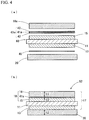
- FIG. 4 shows a manufacturing method of a power-module substrate unit 52 of a third embodiment.
- the circuit layer 18 is formed as the second embodiment, so that the first layer 15 and the second layer 16 are bonded by the double-side clad brazing material 43a in which the brazing material layers 42 are formed on both surfaces of the circuit-side bonding core 41 a.
- the metal layer 13 and the heat sink 20 are bonded by brazing material 45 of Al-Si based alloy as the first embodiment.
- a first bonding process is performed by brazing of bonding the first layer 15 of the circuit layer 18 to one surface of the ceramic substrate 11 and bonding the metal layer 13 to another surface of the ceramic substrate 11 (refer to the part (a) of FIG. 1 ) using the brazing material 40. After that, as shown in a part (a) of FIG.
- a thin aluminum alloy layer (the circuit-side bonding core 41 a of the double-side clad brazing material 43a) is arranged between the first layer 15 and the second layer 16 of the circuit layer 18.
- a ratio (t1 ⁇ A1 ⁇ 1+t3 ⁇ A3 ⁇ 3)/ (t2 ⁇ A2 ⁇ 2) is 0.85 or larger and 1.40 or smaller where t1 is a thickness of the second layer 16 of the circuit layer 18, A1 is a bonding area of the second layer 16 to the circuit-side bonding core 41 a, ⁇ 1 is a yield stress of the second layer 16, t2 is a thickness of the heat sink 20, A2 is a bonding area of the metal layer 13 and the heat sink 20, ⁇ 2 is a yield stress of the heat sink 20, t3 is a thickness of the circuit-side bonding core 41 a, A3 is a bonding area of the circuit-side bonding core 41a and the first layer 15, and ⁇ 3 a yield stress of the circuit-side bonding core 41a.
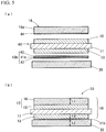
- FIG. 5 shows a manufacturing method of a power-module substrate unit 53 of a fourth embodiment.
- the second layer 16 of the circuit layer 12 is made by bonding a clad plate 19 in which a brazing material layer 44 made of Al-Si-Mg based alloy is stacked on one surface of the second-layer aluminum plate 16a.
- a brazing material layer 44 made of Al-Si-Mg based alloy is stacked on one surface of the second-layer aluminum plate 16a.
- the heat sink 20 is stacked on the metal layer 13 with the double-side clad brazing material 43b (which is constructed by forming the brazing material layers 42 on both the surfaces of the heat-radiation-side bonding core 41b and used in the second embodiment) therebetween, these members are pressed in the stacking direction and heated in non-oxidation atmosphere such as nitrogen atmosphere so as to be brazed.
- the double-side clad brazing material 43b which is constructed by forming the brazing material layers 42 on both the surfaces of the heat-radiation-side bonding core 41b and used in the second embodiment
- a ratio (t1 ⁇ A1 ⁇ 1) / (t2 ⁇ A2 ⁇ 2+t4 ⁇ A4 ⁇ 4) is 0.85 or larger and 1.40 or smaller where t1 is a thickness of an aluminum plate of the second layer 16 of the circuit layer 12, A1 is a bonding area of the second layer 16 and the first layer 15, ⁇ 1 is a yield stress of the second layer 16, t2 is a thickness of the heat sink 20, A2 is a bonding area of the heat sink 20 and the heat-radiation-side bonding core 41b, ⁇ 2 is a yield stress of the heat sink 20, t4 is a thickness of the heat-radiation-side bonding core 41b, A4 is a bonding area of the heat-radiation-side bonding core 41b and the metal layer 13, and ⁇ 4 is a yield stress of the heat-radiation-side bonding core 41b.
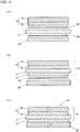
- FIG. 6 shows a manufacturing method of a power-module substrate unit 54 of a fifth embodiment.
- the circuit layer 12 is made as a clad material in which the first layer 15 and the second layer 16 are bonded in advance.
- the circuit layer 12 of the clad material is stacked on one surface of the ceramic substrate 11 with the brazing material 40 made of Al-Si based alloy therebetween, and the metal layer 13 is stacked on another surface of the ceramic substrate 11 with the brazing material 40 made of Al-Si based alloy therebetween, and then these members are heated in a state of being pressed under vacuum atmosphere so as to be brazed (a first bonding process). Consequently, the power-module substrate 10 in which the circuit layer 12 and the metal layer 13 are bonded on both the surfaces of the ceramic substrate 11 is manufactured (a part (b) of FIG. 6 ).
- the heat sink 20 is stacked on the metal layer 13 of the obtained power-module substrate 10 with the brazing material 45 made of Al-Si-Mg based alloy therebetween, and these members are brazed by heating under non-oxidation atmosphere such as nitrogen atmosphere in a pressed state (a second bonding process).
- a ratio (t1 ⁇ A1 ⁇ 1) / (t2 ⁇ A2 ⁇ 2) is 0.85 or larger and 1.40 or smaller when t1 is a thickness of the second layer 16 of the circuit layer 12, A1 is a bonding area of the second layer 16 and the first layer 15, ⁇ 1 is a yield stress of the second layer 16, t2 is a thickness of the heat sink 20, A2 is a bonding area of the metal layer 13 and the heat sink 20, and ⁇ 2 is a yield stress of the heat sink 20.
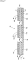
- FIG. 7 shows a power-module substrate unit 55 of a sixth embodiment.
- shapes in which one power-module substrate is bonded on one heat sink are described.
- the present invention can be also applied to a case in which a plurality of power-module substrates 10S are bonded on one heat sink 20 as the power-module substrate unit 55 shown in FIG. 7 .
- the highly-integrated substrate can be obtained by bonding the plurality of power-module substrates 10S on the heat sink 20 at spaces.
- the power-module substrates 10S each are formed by stacking a small-circuit layer 12S which is formed by stacking the first layer 15 and the second layer 16, a small-ceramic substrate 11S, and a small-metal layer 13S.
- a ratio (t1 ⁇ A1 ⁇ 1) / (t2 ⁇ A2 ⁇ 2) is 0.85 or larger and 1.40 or smaller where t1 is a thickness of the second layer 16, A1 is a bonding area of the second layer 16 and the first layer 15 (in this case, A1 is a total of the bonding areas of the second layers 16 and the first layers 15 in the small-circuit layers 12S constructing the circuit layer 12), ⁇ 1 is a yield stress of the second layer 16, t2 is a thickness of the heat sink 20, A2 is a bonding area of the heat sink 20 and the metal layer 13 constructed from the plurality of small metal layers 13S (in this case, A2 is a total of the bonding areas of the small-metal layers 13S to the heat sink 20), and ⁇ 2 is a yield stress of the heat sink 20.
- the warp can be reliably prevented from generating.
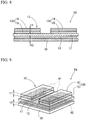
- FIG. 8 and FIG. 9 show a power-module substrate unit 56 of a seventh embodiment.
- the metal layer 13 and the ceramic substrate 11 are respectively formed from one plate, and the circuit layer 12 is formed from the plurality of small-circuit layers 12S which are arranged on the ceramic substrate 11 with space along a surface direction.
- the present invention can be applied also to a case in which the circuit layer 12 is formed from the separated plurality of small-circuit layers 12S.
- the highly-integrated substrate can be obtained similarly to the power-module substrate unit 55 of the sixth embodiment.
- the small-circuit layers 12S in the power-module substrate 56 are formed respectively by stacking the first layer 15 and the second layer 16.
- a ratio (t1 ⁇ A1 ⁇ 1)/ (t2 ⁇ A2 ⁇ 2) is 0.85 or larger and 1.40 or smaller where t1 is a thickness of the second layer 16, A1 is a bonding area of the second layer 16 and the first layer 15 (in this case, A1 is a total of the bonding areas of the second layers 16 and the first layers 15 in the small-circuit layers 12S constructing the circuit layer 12), ⁇ 1 is a yield stress of the second layer 16, t2 is a thickness of the heat sink 20, A2 is a bonding area of the heat sink 20 and the metal layer 13, and ⁇ 2 is a yield stress of the heat sink 20.
- the circuit layer 12 is formed from the plurality of small-circuit layers 12S which are separated from each other as in the power-module substrate unit 56, shapes of the circuit layer 12 and the metal layer 13 which are bonded on the ceramic substrate 11 are different though, in bonding parts, by considering symmetry of the rigidity of the second layer 16 (an yield stress considering a volume multiplying the thickness t1 and the bonding area A1) and the rigidity of the heat sink 20 (an yield stress considering a volume multiplying the thickness t2 and the bonding area A2), the warp can be reliably prevented from generating.
- examples 1 to 18 of the present invention ceramic substrates made of AlN having thickness of 0.635 mm and first layers and metal layers made of 4N-Al having thickness of 0.6 mm were prepared, and second layers of circuit layers and heat sinks having thicknesses, bonding areas, aluminum purities, and yield stresses shown in Table 1 were prepared.
- the heat sinks were a flat plate shape with a whole plane size of 60 mm ⁇ 50 mm.
- “Ratio” in Table 1 denotes (t1 ⁇ A1 ⁇ 1) / (t2 ⁇ A2 ⁇ 2) where the embodiment No. (the bonding method) was 1 or 5, (t1 ⁇ A1 ⁇ 1+t3 ⁇ A3 ⁇ 3) / (t2 ⁇ A2 ⁇ 2+t4 ⁇ A4 ⁇ 4) where the embodiment No. (the bonding method) was 2, (t1 ⁇ A1 ⁇ 1+t3 ⁇ A3 ⁇ 3) / (t2 ⁇ A2 ⁇ 2) where the embodiment No. (the bonding method) was 3, and (t1 ⁇ A1 ⁇ 1) / (t2 ⁇ A2 ⁇ 2+t4 ⁇ A4 ⁇ 4) where the embodiment No. (the bonding method) was 4.
- warp size primary warp
- warp size warp after heating
- the warp sizes were evaluated by fluctuation of flatness at a back surface of the heat sink measured by a moire-type three-dimensional shape measuring device.
- the warp sizes were positive value (+) when the warp was protruded to the circuit layer side, or were negative value (-) when the warp was dented at the circuit layer side. Table 1 shows the results.
- the warp size could be further reduced in the examples 1 to 14 in which (t1 ⁇ A1 ⁇ 1) / (t2 ⁇ A2 ⁇ 2), (t1 ⁇ A1 ⁇ 1+t3 ⁇ A3 ⁇ 3) / (t2 ⁇ A2 ⁇ 2+t4 ⁇ A4 ⁇ 4), or (t1 ⁇ A1 ⁇ 1+t3 ⁇ A3 ⁇ 3) / (t2 ⁇ A2 ⁇ 2), (t1 ⁇ A1 ⁇ 1)/ (t2 ⁇ A2 ⁇ 2+t4 ⁇ A4 ⁇ 4) were in a range of 0.85 or larger and 1.40 or smaller. Accordingly, in the power-module substrate unit, the reliability can be held for a long term since the warp can be prevented from generating if it is exposed to high temperature when the semiconductor element is soldered or in the usage environment after that.
- the heat sinks had the flat plate shape in the above embodiments though, the heat sink may have a shape in which multi-pin fin or belt fin is formed on a flat plate part on which the metal layer is bonded.
- the thickness t2 is a thickness of the flat plate part.
- a power-module substrate unit with heat sink and a power module in which not only a warp (a primary warp) is small after bonding a heat sink, but also a warp in a mounting process of semiconductor elements or in an usage environment is small.
Landscapes
- Engineering & Computer Science (AREA)
- Chemical & Material Sciences (AREA)
- Ceramic Engineering (AREA)
- Materials Engineering (AREA)
- Structural Engineering (AREA)
- Organic Chemistry (AREA)
- Manufacturing & Machinery (AREA)
- Microelectronics & Electronic Packaging (AREA)
- Inorganic Chemistry (AREA)
- Cooling Or The Like Of Semiconductors Or Solid State Devices (AREA)
- Ceramic Products (AREA)
- Structure Of Printed Boards (AREA)
- Parts Printed On Printed Circuit Boards (AREA)
- Physics & Mathematics (AREA)
- Geometry (AREA)
Abstract
Description
- The present invention relates to a power-module substrate unit and a power module used for a semiconductor device controlling large current and high voltage.
- Priority is claimed on
Japanese Patent Application No. 2014-92054, filed April 25, 2014 - For a power module for vehicle, a power-module substrate unit with heat sink constructed by bonding an aluminum plate on a ceramic substrate such as aluminum nitride and bonding an aluminum based heat sink on one surface of the ceramic substrate with an intervening aluminum plate is used.
- The power-module substrate unit with heat sink is conventionally produced as below. First, aluminum plates are respectively bonded on both surface of a ceramic substrate by stacking the aluminum plates on both the surfaces of the ceramic substrate with intervening brazing material suitable for bonding the ceramic substrate and the aluminum plates, and heating them up to temperature above a melting point of the brazing material while pressing at a certain pressure. Then, a heat sink and one of the aluminum plates are bonded by stacking the heat sink on the aluminum plate with intervening brazing material suitable for bonding the aluminum plate and the heat sink, and heating them up to temperature above a melting point of the brazing material while pressing at a certain pressure. As a result, the power-module substrate unit with heat sink can be produced.
- In this power-module substrate unit with heat sink, one of the aluminum plates is formed as a circuit layer on which semiconductor elements such as power devices and the like are mounted by solder material.
- In this power-module substrate, a warp of the substrate should be small since heat radiation performance or the like is deteriorated by the warp.
- Conventionally, there are approaches to reduce the warp or the like of the power-module substrate, as described in Patent Document 1 and Patent Document 2 for example.
- A power module substrate described in Patent Document 1 uses a clad material for a metal plate as a circuit layer, formed by stacking two or more layers including a first layer of aluminum purity of 99.0 mass% or higher and 99.95 mass% or lower and a second layer of aluminum purity of 99.99 mass% or higher. The second layer is bonded to the ceramic substrate. It is described that in this case, a thickness of the circuit layer is 600 µm and a thickness of a metal layer provided on an opposite surface to the circuit layer of the ceramic substrate is 400 µm.
- In Patent Document 2, a silicon nitride circuit substrate in which a metal clad material is bonded to at least one surface of a silicon nitride substrate is disclosed. As the metal clad material, it is described that a combination of conductive material such as a Cu plate, an A1 plate or the like and low thermal expansion metal such as a kovar plate, a tungsten plate or the like is appropriate.
-
- Patent Document 1:
Japanese Unexamined Patent Application, First Publication No. 2012- 191004 - Patent Document 2:
Japanese Unexamined Patent Application, First Publication No. 2003- 168770 - In the conventional power-module substrate unit with heat sink, mainly, it is a subject to reduce a primary warp resulting from difference of linear expansion between an insulate substrate and a heat sink when bonding the heat sink. However, a warp may be generated by temperature fluctuation after bonding the heat sink, in a heating process of mounting semiconductor elements or in a usage environment.
- If the warp is generated in the mounting process, there is a subject of deterioration of bonding reliability since a position of a solder bonding part may be shifted or distortion and cracks may be generated at the solder bonding part. If the warp is generated in the usage environment, thermal conductive grease between the heat sink and a cooler may flow out by a pump-out phenomenon, so that adhesion of the heat sink and the cooler may be deteriorated, as a result, thermal resistance may be increased.
- The present invention is achieved in consideration of the above circumstances, and has an object to provide a power-module substrate unit with heat sink and a power module in which a warp is small not only after bonding a heat sink but also in a mounting process of semiconductor elements or in an usage environment.
- A power-module substrate unit of the present invention having at least one power-module substrate including one ceramic substrate, a circuit layer formed on one surface of the ceramic substrate, and a metal layer formed on another surface of the ceramic substrate, and a heat sink on which the metal layer of the power-module substrate is bonded, the power-module substrate unit in which the metal layer is made of an aluminum plate having purity of 99.99 mass% or higher; the heat sink is formed from an aluminum plate having purity of 99.90 mass% or lower; and the circuit layer has a stacking structure of a first layer made of an aluminum plate having purity of 99.99 mass% or higher and being bonded to the ceramic substrate; and a second layer made of an aluminum plate having purity lower than 99.90 mass% and being bonded on a surface of the first layer.
- Since the circuit layer has a stacked structure of the first and second layers, and the second layer made of the aluminum plate having high rigidity is arranged on the ceramic substrate of an opposite side to the heat sink having high rigidity, i.e., high yield stress, accordingly, the heat sink and the second layer of the circuit layer are arranged symmetrically about the ceramic substrate. As a result, a warp is hardly generated because internal stresses act on both surfaces of the ceramic substrate by heating are balanced. As the first layer bonded to the ceramic substrate, the aluminum plate having purity of 99.99 mass% or higher, which is comparatively soft, i.e., having low yield stress, is arranged; accordingly, cracks can be prevented by reducing thermal stress which acts on the ceramic substrate by heating. Moreover, in a case in which the second layer is made of an aluminum plate with high yield stress having purity lower than 99.90 mass%, a thickness of the second layer can be small, so that a structure can be more desirable since the thermal resistance is not increased.
- In the power-module substrate unit of the present invention, it is preferable that a ratio (t1×A1×σ1) / (t2×A2×σ2) be 0.85 or larger and 1.40 or smaller: where t1 (mm) is a thickness of the second layer; A1 (mm2) is a bonding area of the second layer; σ1 (N/mm2) is a yield stress of the second layer; t2 (mm) is a thickness of the heat sink; A2 (mm2) is a bonding area of the heat sink; and σ2 (N/mm2) is a yield stress of the heat sink.
- For the second layer of the circuit layer and the heat sink, by setting relation between the thicknesses, the bonding areas and the yield stresses to these ranges, it is possible to improve symmetry around the ceramic substrate, so the warp can be reliably prevented. That is to say, in a case in which the circuit layer is constructed as a pattern by arranging a plurality of small-circuit layers on the ceramic substrate of the power-module substrate unit, the warp can be reliably prevented by considering the symmetry between rigidity of the second layer and rigidity of the
heat sink 20 at the bonding parts, though outlines are different between the bonding part of the circuit layer which is bonded to the ceramic substrate and the bonding part of the heat sink to which the metal layer is bonded. - In the power-module substrate unit of the present invention, the circuit layer may further include a circuit-side bonding core made of an aluminum alloy plate between the first layer and the second layer: and a ratio (t1 ×A1 ×σ1+t3×A3×σ3) / (t2×A2×σ2) may be 0.85 or larger and 1.40 or smaller: where t1 (mm) is a thickness of the second layer; A1 (mm2) is a bonding area of the second layer; σ1 (N/mm2) is a yield stress of the second layer; t2 (mm) is a thickness of the heat sink; A2 (mm2) is a bonding area of the heat sink; σ2 (N/mm2) is a yield stress of the heat sink; t3 (mm) is a thickness of the circuit-side bonding core; A3 (mm2) is a bonding area of the circuit-side bonding core and the first layer; and σ3 (N/mm2) a yield stress of the circuit-side bonding core.
- The power-module substrate unit of the present invention further may include a heat-radiation-side bonding core made of an aluminum alloy plate between the metal layer and the heat sink, and a ratio (t1×A1×σ1) / (t2×A2×σ2+t4×A4×σ4) is 0.85 or larger and 1.40 or smaller, where t1 (mm) is a thickness of the second layer; A1 (mm2) is a bonding area of the second layer; σ1 (N/mm2) is a yield stress of the second layer; t2 (mm) is a thickness of the heat sink; A2 (mm2) is a bonding area of the heat sink; σ2 (N/mm2) is a yield stress of the heat sink; t4 (mm) is a thickness of the heat-radiation-side bonding core; A4 (mm2) is a bonding area of the heat-radiation-side bonding core and the metal layer; and σ4 (N/mm2) is a yield stress of the heat-radiation-side bonding core.
- In the power-module substrate unit of the present invention, the circuit layer may further include a circuit-side bonding core made of an aluminum alloy plate between the first layer and the second layer, and a heat-radiation-side bonding core made of an aluminum alloy plate between the metal layer and the heat sink, and a ratio (t1 ×A1 ×σ1+t3×A3×σ3) / (t2×A2×σ2+t4×A4×σ4) may be 0.85 or larger and 1.40 or smaller, where: t1 (mm) is a thickness of the second layer; A1 (mm2) is a bonding area of the second layer; σ1 (N/mm2) is a yield stress of the second layer; t2 (mm) is a thickness of the heat sink; A2 (mm2) is a bonding area of the heat sink; σ2 (N/mm2) is a yield stress of the heat sink; t3 (mm) is a thickness of the circuit-side bonding core; A3 (mm2) is a bonding area of the circuit-side bonding core and the first layer; σ3 (N/mm2) is a yield stress of the circuit-side bonding core; t4 (mm) is a thickness of the heat-radiation-side bonding core; A4 (mm2) is a bonding area of the heat-radiation-side bonding core and the metal layer; and σ4 (N/mm2) is a yield stress of the heat-radiation-side bonding core.
- In the power-module substrate unit of the present invention, the circuit layer of the power module substrate may be formed of a plurality of small-circuit layers which are separated from each other.
- The power-module substrate unit of the present invention may include a plurality of the power-module substrates.
- A power module of the present invention includes the power-module substrate unit and a semiconductor element mounted on a surface of the circuit layer.
- According to the present invention, by reducing the warp caused by heating, it is possible to resolve the problem in the processes to mount the semiconductor elements by soldering or the like, and reliability of an insulate substrate is improved since the warp by a temperature cycle is reduced. Moreover, deformation of the circuit layer is reduced by using a high-rigid member for the circuit layer, and contact reliability of the semiconductor element is also good.
-
-
FIG. 1 is a sectional view showing a manufacturing process of a power-module substrate unit according to a first embodiment of the present invention. -
FIG. 2 is a front view of a pressing device used for manufacturing the power-module substrate unit according to the first embodiment of the present invention. -
FIG. 3 is a sectional view showing a manufacturing process of a power-module substrate unit according to a second embodiment of the present invention. -
FIG. 4 is a sectional view showing a manufacturing process of a power-module substrate unit according to a third embodiment of the present invention. -
FIG. 5 is a sectional view showing a manufacturing process of a power-module substrate unit according to a fourth embodiment of the present invention. -
FIG. 6 is a sectional view showing a manufacturing process of a power-module substrate unit according to a fifth embodiment of the present invention. -
FIG. 7 is a sectional view of a power-module substrate unit according to a sixth embodiment of the present invention. -
FIG. 8 is a sectional view of a power-module substrate unit according to a seventh embodiment of the present invention. -
FIG. 9 is a perspective view showing the power-module substrate unit ofFIG. 8 . - Below, embodiments of the present invention will be explained referring drawings. A power-
module substrate unit 50 of a first embodiment shown in a part (c) ofFIG. 1 is provided with a power-module substrate 10 and aheat sink 20. Apower module 100 is manufactured by mounting asemiconductor element 30 such as a semiconductor chip and the like on a surface of the power-module substrate unit 50. - The power-
module substrate 10 is provided with aceramic substrate 11, acircuit layer 12 bonded on one surface of theceramic substrate 11 by soldering, and ametal layer 13 bonded on another surface of theceramic substrate 11 by soldering. Regarding this power-module substrate 10, thesemiconductor element 30 is soldered on a surface of thecircuit layer 12, and theheat sink 20 is brazed on a surface of themetal layer 13. - The
ceramic substrate 11 can be made of, for example, nitride-ceramics such as AlN (aluminum nitride), Si3N4 (silicon nitride) or the like, or oxide-ceramics such as Al2O3 (alumina) or the like. Thickness of theceramic substrate 11 can be set in a range of 0.2 to 1.5 mm. - The
circuit layer 12 has a stacking structure of afirst layer 15 bonded on the surface of theceramic substrate 11, and asecond layer 16 bonded on thefirst layer 15. Thefirst layer 15 is made of an aluminum plate having purity of 99.99 mass% or higher (i.e., a pure aluminum plate of 1N99 of the JIS standard: so-called a 4N aluminum). Thesecond layer 16 is made of an aluminum plate having purity lower than 99.90 mass% (i.e., a pure aluminum plate having purity of 99.0 mass% or higher, so-called 2N aluminum of the JIS standard (e.g., A1050 or the like), or an aluminum alloy plate such as A3003, A6063, A5052 or the like of the JIS standard. Thickness of thefirst layer 15 is 0.1 mm or more and 2.5 mm or less, and thickness t1 of thesecond layer 16 is 0.5 mm or more and 5.0 mm or less. - The
metal layer 13 is made of an aluminum plate having purity of 99.99 mass% or higher (1N99 of the JIS standard (purity of 99.99 mass% or higher: so-called 4N aluminum), and formed to have thickness of 0.1 mm or more and less than 2.5 mm, similar to thefirst layer 15 of thecircuit layer 12. - As material of the
heat sink 20 bonded to the power-module substrate 10, an aluminum plate having purity of 99.90 mass% or lower such as 1N90 of the JIS standard (purity of 99.90 mass% or higher, so-called 3N aluminum) or so-called 2N aluminum having purity of 99.0 mass% or higher (e.g., A1050 or the like), or an aluminum alloy plate such as A3003, A6063, A5052 or the like can be used. - As the
heat sink 20, such as a shape of plane plate, a shape of multi-pin fin integrally formed by hot forging or the like, a shape of fin integrally formed by extrusion molding to have belt fin which are parallel to each other or the like, an appropriate one can be used. Theheat sink 20 is assembled as a part of a cooler in which coolant is circulated, to the other parts of the cooler by screws or the like. Especially, it is preferable to use the flat plate in which efficient of reducing the warp is large or the one integrally formed with multi-pin fin as theheat sink 20. In this embodiment, theheat sink 20 has a flat plate shape. - The
heat sink 20 and thesecond layer 16 of thecircuit layer 12 are set to have a ratio of (t1×A1×σ1) / (t2×A2×σ2) in 0.85 or larger and 1.40 or smaller where t1 is the thickness of thesecond layer 16, A1 is a bonding area of thesecond layer 16 to thefirst layer 15, σ1 is an yield stress of thesecond layer 16, t2 is a thickness of theheat sink 20, A2 is a bonding area of themetal layer 13 to theheat sink 20, and σ2 is an yield stress of theheat sink 20. - For example, in a case in which the
second layer 16 is aluminum alloy of A5003 (the yield stress σ1=40 N/mm2) having the thickness t1=1.5 mm, the bonding area A1 of thefirst layer 15 and thesecond layer 16 is 900 mm2, theheat sink 20 is made of aluminum alloy of A6063 (the yield stress σ2=50 N/mm2) having the thickness t2=1.0 mm, and the bonding area A2 of themetal layer 13 and theheat sink 20 is 1000 mm2, the ratio of (t1×A1×σ1) / (t2×A2×σ2) =1.08. The values of the yield stress in the present invention are values at room temperature (25°C). - Next, a method for manufacturing the power-
module substrate unit 50 constructed as above will be explained. The power-module substrate unit 50 is manufactured by bonding thefirst layer 15 of thecircuit layer 12 and themetal layer 13 to the ceramic substrate 11 (a first bonding process), and then bonding thesecond layer 16 on thefirst layer 15 and theheat sink 20 on the metal layer 13 (a second bonding process). Below, the processes will be explained in order. - First, as shown by a part (a) of
FIG. 1 , stacking a first-layer aluminum plate 15a to be thefirst layer 15 of thecircuit layer 12 on one surface of theceramic substrate 11, and stacking a metal-layer aluminum plate 13a to be themetal layer 13 on another surface of theceramic substrate 11, these members are bonded together. For bonding these members, brazingmaterial 40 of Al-Si based alloy or the like is used. It is preferable that thebrazing material 40 be a form of a foil. - As shown by the part (a) of
FIG. 1 , theceramic substrate 11, the first-layer aluminum plate 15a and the metal-layer aluminum plate 13a are stacked with thebrazing materials 40 therebetween so as to be a stacked body S. The stacked bodies S are pressed in a stacking direction by apressing device 110 as shown inFIG. 2 . - The
pressing device 110 is provided with abase plate 111, guide posts 112 vertically fixed to four corners of an upper surface of thebase plate 111, afixed plate 113 fixed to upper ends of the guidingposts 112, apressing plate 114 held by the guidingposts 112 between thebase plate 111 and the fixedplate 113 so as to move vertically, and apressing means 115 such as a spring between thefixed plate 113 and thepressing plate 114 so as to press thepressing plate 114 downward. - The fixed
plate 113 and thepressing plate 114 are arranged parallel to thebase plate 111. The stacked bodies S are disposed between thebase plate 111 and thepressing plate 114.Carbon sheets 116 are disposed at both sides of the stacked bodies S in order to average pressing force. - Brazing is performed by heating up to brazing temperature under vacuum atmosphere by the
pressing device 110 in a heating furnace (not illustrated) in a pressed state by thepressing device 110. In this circumstance, the pressing force is set to 0.68 MPa (7 kgf/cm2) and heating temperature is set to 640°C, for example. - As shown in a part (b) of
FIG. 1 , on thefirst layer 15 of thecircuit layer 12 in a bondedbody 60 obtained by the first bonding process, a second-layer aluminum plate 16a to be thesecond layer 16 with thebrazing material 40 therebetween is stacked, and theheat sink 20 is stacked on themetal layer 13 with thebrazing material 40 therebetween. Thesebrazing materials 40 are used as foils of brazing material of Al-Si based alloy or the like. - Then, stacked bodies of these are pressed in a stacking direction by the
pressing device 110 as inFIG. 2 , and heated under vacuum atmosphere as it is together with thepressing device 110 so that thesecond layer 16 and theheat sink 20 are brazed. In this circumstance, pressing force is set to 0.68 MPa (7 kgf/cm2) and heating temperature is set to 615°C, for example. - On the power-
module substrate unit 50 manufactured as above, thesemiconductor element 30 is bonded by soldering at an upper surface of the circuit layer 12 (the second layer 16) as shown in the part (c) ofFIG. 1 , so that thepower module 100 is manufactured. - In the
power module 100 manufactured as above, the power-module substrate unit 50 has thecircuit layer 12 as a stacking structure of thefirst layer 15 and thesecond layer 16, so that thesecond layer 16 formed from the second-layer aluminum plate 16a having high rigidity is arranged at an opposite side to theceramic substrate 11 with respect to theheat sink 20 having high rigidity, i.e., having high yield stress, so that theheat sink 20 and thesecond layer 16 of thecircuit layer 12 are symmetrically arranged about theceramic plate 11. Accordingly, internal stresses act on both surfaces of theceramic substrate 11 by heating are balanced, and a warp is hardly generated. Furthermore, since the first-layer aluminum plate 15a, which is comparatively soft and has purity of 99.99 mass% or higher, i.e., has low yield stress, is arranged as thefirst layer 15 bonded to theceramic substrate 11, thermal stress on theceramic substrate 11 when it is heated can be reduced, so that breakage can be prevented. Moreover, if thesecond layer 16 is made of an aluminum plate having purity lower than 99.90 mass% with high yield stress, thickness of thesecond layer 16 can be decreased, so that it is a more preferable structure since the thermal resistance is not increased. - In the power-
module substrate unit 50, the ratio (t1 ×A1 ×σ1) / (t2×A2×σ2) is set to 0.85 or larger and 1.40 or smaller, where t1 is the thickness of thesecond layer 16 of thecircuit layer 12, A1 is the bonding area of thefirst layer 15 and thesecond layer 16, σ1 is the yield stress of thesecond layer 16, t2 is the thickness of theheat sink 20, A2 is the bonding area of themetal layer 13 and theheat sink 20, and σ2 is the yield stress of theheat sink 20. As a result, the warp caused from temperature fluctuation in the mounting process of thesemiconductor element 30 and or in the usage environment after that is hardly generated, so the power-module substrate unit 50 has long term high reliability as a insulate substrate. - In the power-
module substrate unit 50, in the cases in which the ratio (t1 ×A1 ×σ1) / (t2×A2×σ2) is 1.00, 0.85 or larger and smaller than 1.00, or larger than 1.00 and 1.40 or smaller, a good symmetry structure about theceramic substrate 11 can be obtained. In the power-module substrate unit 50, deformation of thecircuit layer 12 can be prevented since thesecond layer 16 on which thesemiconductor element 30 is soldered is made of an aluminum plate with high rigidity, i.e., high yield stress. - For soldering the
semiconductor element 30, Sn-Sb based, Sn-Ag based, Sn-Cu based, Sn-In based or Sn-Ag-Cu based soldering material is used, and it is performed by heating to 275°C to 335 °C, for example. - In the above first embodiment, the brazing material of Al-Si based alloy is used for brazing in vacuum atmosphere. Moreover, Al-Si-Mg based, Al-Mg based, Al-Ge based, Al-Cu based, or Al-Mn based brazing material can be used. In a case in which brazing material of Al-Si-Mg based alloy or Al-Mg based alloy including Mg is used for brazing, it can be performed in non-oxidation atmosphere.
-
FIG. 3 shows a manufacturing method of a power-module substrate unit 51 of a second embodiment. In this embodiment, same reference symbols are denoted on same elements as in the first embodiment shown inFIG. 1 . (It is the same in embodiments mentioned below.) - In the power-
module substrate unit 51, a double-side cladbrazing material 43a in which brazing material layers 42 are formed on both surface of a circuit-side bonding core 41a bonds thefirst layer 15 and thesecond layer 16 of acircuit layer 18 in a power-module substrate 17. Themetal layer 13 and theheat sink 20 are bonded by a double-side cladbrazing material 43b in which brazing material layers 42 are formed on both surface of a heat-radiation-side bonding core 41 b. - In the double-side clad
brazing materials side bonding core 41a and the heat-radiation-side bonding core 41b are made of A3003 aluminum alloy by the JIS standard having thickness of 0.05 mm to 0.6 mm, and the brazing material layers 42 at both sides are made of Al-Si-Mg based alloy. - The manufacturing method of the power-
module substrate unit 51 of the second embodiment will be explained. First, similar to the first bonding process of the first embodiment, a first bonding process by brazing is performed using thebrazing material 40, by bonding thefirst layer 15 of thecircuit layer 18 to one surface of theceramic substrate 11, and bonding themetal layer 13 to another surface of the ceramic substrate 11 (refer to the part (a) ofFIG. 1 ). After that, as shown in a part (a) ofFIG. 3 , stacking the second-layer aluminum plate 16a to be thesecond layer 16 on thefirst layer 15 with the double-side cladbrazing material 43a therebetween, and stacking theheat sink 20 on themetal layer 13 with the double-side cladbrazing material 43b therebetween, and these members are brazed by pressing in the stacking direction and heating in non-oxidation atmosphere such as nitrogen atmosphere. - In the power-
module substrate unit 51 of the second embodiment manufactured as above, as shown in a part (b) ofFIG. 3 , a thin aluminum alloy layer (the circuit-side bonding core 41 a) is arranged between thefirst layer 15 and thesecond layer 16 of thecircuit layer 18, and a thin aluminum alloy layer (the heat-radiation-side bonding core 41b) is arranged between themetal layer 13 and theheat sink 20. - In the power-
module substrate unit 51, a ratio (t1×A1 ×σ1+t3×A3×σ3) / (t2×A2×σ2+t4×A4×σ4) is 0.85 or larger and 1.40 or smaller, where t1 is a thickness of thesecond layer 16 in thecircuit layer 18, A1 is a bonding area of thesecond layer 16 to the circuit-side bonding core 41a, σ1 is a yield stress of thesecond layer 16, t2 is a thickness of theheat sink 20, A2 is a bonding area of theheat sink 20 to the heat-radiation-side bonding core 41b, σ2 is a yield stress of theheat sink 20, t3 is a thickness of the circuit-side bonding core 41 a, A3 a bonding area of the circuit-side bonding core 41 a and thefirst layer 15, σ3 is a yield stress of the circuit-side bonding core 41a, t4 is a thickness of the heat-radiation-side bonding core 41b, A4 is a bonding area of the heat-radiation-side bonding core 41b and themetal layer 13, and σ4 is a yield stress of the heat-radiation-side bonding core 41b. - In the power-
module substrate unit 51, as described above, when the ratio (t1 ×A1 ×σ1+t3×A3×σ3) / (t2×A2×σ2+t4×A4×σ4) is 1.00, 0.85 or larger and smaller than 1.00, or larger than 1.00 and 1.40 or smaller, a good symmetry structure about theceramic substrate 11 can be obtained as in the first embodiment. -
FIG. 4 shows a manufacturing method of a power-module substrate unit 52 of a third embodiment. In the power-module substrate unit 52, thecircuit layer 18 is formed as the second embodiment, so that thefirst layer 15 and thesecond layer 16 are bonded by the double-side cladbrazing material 43a in which the brazing material layers 42 are formed on both surfaces of the circuit-side bonding core 41 a. Themetal layer 13 and theheat sink 20 are bonded by brazingmaterial 45 of Al-Si based alloy as the first embodiment. - The manufacturing method of the power-
module substrate unit 52 of the third embodiment will be explained. First, similar to the first bonding process of the first embodiment, a first bonding process is performed by brazing of bonding thefirst layer 15 of thecircuit layer 18 to one surface of theceramic substrate 11 and bonding themetal layer 13 to another surface of the ceramic substrate 11 (refer to the part (a) ofFIG. 1 ) using thebrazing material 40. After that, as shown in a part (a) ofFIG. 4 , stacking the second-layer aluminum plate 16a to be thesecond layer 16 on thefirst layer 15 with the double-side cladbrazing material 43a therebetween, and stacking theheat sink 20 on themetal layer 13 with thebrazing material 45 made of Al-Si-Mg based alloy, and these members are brazed by pressing in the stacking direction and heating in non-oxidation atmosphere such as nitrogen-atmosphere. - In this power-
module substrate unit 52, as shown in a part (b) ofFIG. 4 , a thin aluminum alloy layer (the circuit-side bonding core 41 a of the double-side cladbrazing material 43a) is arranged between thefirst layer 15 and thesecond layer 16 of thecircuit layer 18. - In this power-
module substrate unit 52, a ratio (t1 ×A1 ×σ1+t3×A3×σ3)/ (t2×A2×σ2) is 0.85 or larger and 1.40 or smaller where t1 is a thickness of thesecond layer 16 of thecircuit layer 18, A1 is a bonding area of thesecond layer 16 to the circuit-side bonding core 41 a, σ1 is a yield stress of thesecond layer 16, t2 is a thickness of theheat sink 20, A2 is a bonding area of themetal layer 13 and theheat sink 20, σ2 is a yield stress of theheat sink 20, t3 is a thickness of the circuit-side bonding core 41 a, A3 is a bonding area of the circuit-side bonding core 41a and thefirst layer 15, and σ3 a yield stress of the circuit-side bonding core 41a. - In the power-
module substrate unit 52, as described above, in cases in which the ratio (t1 ×A1 ×σ1+t3×A3×σ3) / (t2×A2×σ2) is 1.00, 0.85 or larger and smaller than 1.00, or larger than 1.00 and 1.40 or smaller, a good symmetry structure about theceramic substrate 11 can be obtained as in the first embodiment. -
FIG. 5 shows a manufacturing method of a power-module substrate unit 53 of a fourth embodiment. In the power-module substrate unit 53, thesecond layer 16 of thecircuit layer 12 is made by bonding aclad plate 19 in which abrazing material layer 44 made of Al-Si-Mg based alloy is stacked on one surface of the second-layer aluminum plate 16a. First, (1) thefirst layer 15 of thecircuit layer 12 is brazed on one surface of theceramic substrate 11 and themetal layer 13 is brazed on another surface of theceramic substrate 11 as in the first bonding process of the first embodiment, then theclad plate 19 is stacked laying thebrazing material layer 44 over thefirst layer 15 as shown in a part (a) ofFIG. 5 , theheat sink 20 is stacked on themetal layer 13 with the double-side cladbrazing material 43b (which is constructed by forming the brazing material layers 42 on both the surfaces of the heat-radiation-side bonding core 41b and used in the second embodiment) therebetween, these members are pressed in the stacking direction and heated in non-oxidation atmosphere such as nitrogen atmosphere so as to be brazed. - In the power-
module substrate unit 53 shown in a part (b) ofFIG. 5 , a ratio (t1 ×A1 ×σ1) / (t2×A2×σ2+t4×A4×σ4) is 0.85 or larger and 1.40 or smaller where t1 is a thickness of an aluminum plate of thesecond layer 16 of thecircuit layer 12, A1 is a bonding area of thesecond layer 16 and thefirst layer 15, σ1 is a yield stress of thesecond layer 16, t2 is a thickness of theheat sink 20, A2 is a bonding area of theheat sink 20 and the heat-radiation-side bonding core 41b, σ2 is a yield stress of theheat sink 20, t4 is a thickness of the heat-radiation-side bonding core 41b, A4 is a bonding area of the heat-radiation-side bonding core 41b and themetal layer 13, and σ4 is a yield stress of the heat-radiation-side bonding core 41b. - In this power-
module substrate unit 53, as described above, in cases in which the ratio (t1 ×A1×σ1) / (t2×A2×σ2+t4×A4×σ4) is 1.00, 0.85 or larger and smaller than 1.00, or larger than 1.00 and 1.40 or smaller, a good symmetry structure about theceramic substrate 11 can be obtained as in the first embodiment. -
FIG. 6 shows a manufacturing method of a power-module substrate unit 54 of a fifth embodiment. In this power-module substrate unit 54, thecircuit layer 12 is made as a clad material in which thefirst layer 15 and thesecond layer 16 are bonded in advance. - As shown in a part (a) of
FIG. 6 , thecircuit layer 12 of the clad material is stacked on one surface of theceramic substrate 11 with thebrazing material 40 made of Al-Si based alloy therebetween, and themetal layer 13 is stacked on another surface of theceramic substrate 11 with thebrazing material 40 made of Al-Si based alloy therebetween, and then these members are heated in a state of being pressed under vacuum atmosphere so as to be brazed (a first bonding process). Consequently, the power-module substrate 10 in which thecircuit layer 12 and themetal layer 13 are bonded on both the surfaces of theceramic substrate 11 is manufactured (a part (b) ofFIG. 6 ). - Next, as shown in the part (b) of
FIG. 6 , theheat sink 20 is stacked on themetal layer 13 of the obtained power-module substrate 10 with thebrazing material 45 made of Al-Si-Mg based alloy therebetween, and these members are brazed by heating under non-oxidation atmosphere such as nitrogen atmosphere in a pressed state (a second bonding process). - In this power-
module substrate unit 54 shown in a part (c) ofFIG. 6 , a ratio (t1 ×A1 ×σ1) / (t2×A2×σ2) is 0.85 or larger and 1.40 or smaller when t1 is a thickness of thesecond layer 16 of thecircuit layer 12, A1 is a bonding area of thesecond layer 16 and thefirst layer 15, σ1 is a yield stress of thesecond layer 16, t2 is a thickness of theheat sink 20, A2 is a bonding area of themetal layer 13 and theheat sink 20, and σ2 is a yield stress of theheat sink 20. - In this power-
module substrate unit 54, as described above, in cases in which the ratio (t1 ×A1 ×σ1) / (t2×A2×σ2) is 1.00, 0.85 or larger and smaller than 1.00, or larger than 1.00 and 1.40 or smaller, a good symmetry structure about theceramic substrate 11 can be obtained as in the first embodiment. -
FIG. 7 shows a power-module substrate unit 55 of a sixth embodiment. In the above first to fifth embodiments, shapes in which one power-module substrate is bonded on one heat sink are described. The present invention can be also applied to a case in which a plurality of power-module substrates 10S are bonded on oneheat sink 20 as the power-module substrate unit 55 shown inFIG. 7 . In the power-module substrate unit 55 constructed as above, the highly-integrated substrate can be obtained by bonding the plurality of power-module substrates 10S on theheat sink 20 at spaces. - In this power-
module substrate unit 55, the power-module substrates 10S each are formed by stacking a small-circuit layer 12S which is formed by stacking thefirst layer 15 and thesecond layer 16, a small-ceramic substrate 11S, and a small-metal layer 13S. A ratio (t1 ×A1 ×σ1) / (t2×A2×σ2) is 0.85 or larger and 1.40 or smaller where t1 is a thickness of thesecond layer 16, A1 is a bonding area of thesecond layer 16 and the first layer 15 (in this case, A1 is a total of the bonding areas of thesecond layers 16 and thefirst layers 15 in the small-circuit layers 12S constructing the circuit layer 12), σ1 is a yield stress of thesecond layer 16, t2 is a thickness of theheat sink 20, A2 is a bonding area of theheat sink 20 and themetal layer 13 constructed from the plurality ofsmall metal layers 13S (in this case, A2 is a total of the bonding areas of the small-metal layers 13S to the heat sink 20), and σ2 is a yield stress of theheat sink 20. - In this power-
module substrate unit 55, as described above, in cases in which the ratio (t1 ×A1×σ1) / (t2×A2×σ2) is 1.00, 0.85 or larger and smaller than 1.00, or larger than 1.00 and 1.40 or smaller, a good symmetry structure about theceramic substrate 11 can be obtained as in the first embodiment. - In a case in which the plurality of power-
module substrates 10S are provided as in the power-module substrate unit 55, in each of bonding parts, by considering symmetry of the rigidity of the second layer 16 (an yield stress considering a volume multiplying the thickness t1 and the bonding area A1) and the rigidity of theheat sink 20, the warp can be reliably prevented from generating. -
FIG. 8 and FIG. 9 show a power-module substrate unit 56 of a seventh embodiment. In this power-module substrate unit 56, themetal layer 13 and theceramic substrate 11 are respectively formed from one plate, and thecircuit layer 12 is formed from the plurality of small-circuit layers 12S which are arranged on theceramic substrate 11 with space along a surface direction. Thus, the present invention can be applied also to a case in which thecircuit layer 12 is formed from the separated plurality of small-circuit layers 12S. In the power-module substrate unit 56 constructed as above, since a pattern of thecircuit layer 12 is formed by bonding the plurality of small-circuit layers 12S with space on theceramic substrate 11, the highly-integrated substrate can be obtained similarly to the power-module substrate unit 55 of the sixth embodiment. - The small-
circuit layers 12S in the power-module substrate 56 are formed respectively by stacking thefirst layer 15 and thesecond layer 16. A ratio (t1×A1×σ1)/ (t2×A2×σ2) is 0.85 or larger and 1.40 or smaller where t1 is a thickness of thesecond layer 16, A1 is a bonding area of thesecond layer 16 and the first layer 15 (in this case, A1 is a total of the bonding areas of thesecond layers 16 and thefirst layers 15 in the small-circuit layers 12S constructing the circuit layer 12), σ1 is a yield stress of thesecond layer 16, t2 is a thickness of theheat sink 20, A2 is a bonding area of theheat sink 20 and themetal layer 13, and σ2 is a yield stress of theheat sink 20. - In this power-
module substrate unit 56, as described above, in cases in which the ratio (t1 ×A1 ×σ1) / (t2×A2×σ2) is 1.00, 0.85 or larger and smaller than 1.00, or larger than 1.00 and 1.40 or smaller, a good symmetry structure about theceramic substrate 11 can be obtained as in the first embodiment. - In a case in which the
circuit layer 12 is formed from the plurality of small-circuit layers 12S which are separated from each other as in the power-module substrate unit 56, shapes of thecircuit layer 12 and themetal layer 13 which are bonded on theceramic substrate 11 are different though, in bonding parts, by considering symmetry of the rigidity of the second layer 16 (an yield stress considering a volume multiplying the thickness t1 and the bonding area A1) and the rigidity of the heat sink 20 (an yield stress considering a volume multiplying the thickness t2 and the bonding area A2), the warp can be reliably prevented from generating. - Next, examples for confirming the effect of the present invention will be explained. For examples 1 to 18 of the present invention, ceramic substrates made of AlN having thickness of 0.635 mm and first layers and metal layers made of 4N-Al having thickness of 0.6 mm were prepared, and second layers of circuit layers and heat sinks having thicknesses, bonding areas, aluminum purities, and yield stresses shown in Table 1 were prepared. The heat sinks were a flat plate shape with a whole plane size of 60 mm × 50 mm.
- These were bonded by the bonding method described in the first to fifth embodiments, so that power-module substrate units were manufactured. "Embodiment No." (the bonding methods) in Table 1 denotes the manufacturing methods of embodiments by which the samples were manufactured. As a conventional example 1, manufactured was a power-module substrate unit in which a second layer was not formed by not bonding the second layer of the circuit layer in the bonding method described in the first embodiment.
- "Ratio" in Table 1 denotes (t1 ×A1 ×σ1) / (t2×A2×σ2) where the embodiment No. (the bonding method) was 1 or 5, (t1×A1×σ1+t3×A3×σ3) / (t2×A2×σ2+t4×A4×σ4) where the embodiment No. (the bonding method) was 2, (t1 ×A1 ×σ1+t3×A3×σ3) / (t2×A2×σ2) where the embodiment No. (the bonding method) was 3, and (t1 ×A1 ×σ1) / (t2×A2×σ2+t4×A4×σ4) where the embodiment No. (the bonding method) was 4.
- About the obtained samples, warp size (primary warp) at normal temperature (25°C) after bonding, and warp size (warp after heating) when heated to 280°C were measured. The warp sizes were evaluated by fluctuation of flatness at a back surface of the heat sink measured by a moire-type three-dimensional shape measuring device. The warp sizes were positive value (+) when the warp was protruded to the circuit layer side, or were negative value (-) when the warp was dented at the circuit layer side. Table 1 shows the results.


- As known from Table 1, in the conventional sample 1 in which the second layer made of an aluminum plate having purity lower than 99.90 mass% were not stacked on the circuit layer, it was confirmed that the warp size was bigger at the normal temperature and when heated. On the other hand, in the invention examples 1 to 18 in which the second layer made of an aluminum plate having purity lower than 99.90 mass% were stacked on the circuit layer, it was confirmed that the power-module substrate unit in which the warp size at the normal temperature and when heated was small can be obtained.
- Furthermore, it was confirmed that the warp size could be further reduced in the examples 1 to 14 in which (t1×A1×σ1) / (t2×A2×σ2), (t1 ×A1×σ1+t3×A3×σ3) / (t2×A2×σ2+t4×A4×σ4), or (t1×A1×σ1+t3×A3×σ3) / (t2×A2×σ2), (t1×A1×σ1)/ (t2×A2×σ2+t4×A4×σ4) were in a range of 0.85 or larger and 1.40 or smaller. Accordingly, in the power-module substrate unit, the reliability can be held for a long term since the warp can be prevented from generating if it is exposed to high temperature when the semiconductor element is soldered or in the usage environment after that.
- The present invention is not limited to the above-described embodiments and various modifications may be made without departing from the scope of the present invention. For example, the heat sinks had the flat plate shape in the above embodiments though, the heat sink may have a shape in which multi-pin fin or belt fin is formed on a flat plate part on which the metal layer is bonded. In this case, the thickness t2 is a thickness of the flat plate part.
- It is possible to provide a power-module substrate unit with heat sink and a power module in which not only a warp (a primary warp) is small after bonding a heat sink, but also a warp in a mounting process of semiconductor elements or in an usage environment is small.
-
- 10
- power-module substrate
- 11
- ceramic substrate
- 11 S
- small-ceramic substrate
- 12
- circuit layer
- 12S
- small-curcuit layer
- 13
- metal layer
- 13S
- small-metal layer
- 13a
- metal-layer aluminum plate
- 15
- first layer
- 15a
- first-layer aluminum
- 16
- second layer
- 16a
- second-layer aluminum plate
- 17
- power-module substrate
- 18
- circuit layer
- 19
- clad plate
- 20
- heat sink
- 30
- semiconductor element
- 40
- brazing material
- 41 a
- circuit-side bonding core
- 41b
- heat-radiation-side bonding core
- 42
- brazing material layer
- 43a, 43b
- double-side clad brazing material
- 44
- brazing material layer
- 45
- brazing material
- 50 to 56
- power-module substrate unit
- 60
- bonded body
- 110
- pressing device
Claims (8)
- A power-module substrate unit comprising at least one power-module substrate comprising one ceramic substrate, a circuit layer formed on one surface of the ceramic substrate, and a metal layer formed on another surface of the ceramic substrate; and a heat sink on which the metal layer of the power-module substrate is bonded, wherein:the metal layer is made of an aluminum plate having purity of 99.99 mass% or higher;the heat sink is formed from an aluminum plate having purity of 99.90 mass% or lower; andthe circuit layer has a stacking structure of a first layer made of an aluminum plate having the purity of 99.99 mass% or higher and being bonded to the ceramic substrate; and a second layer made of an aluminum plate having the purity lower than 99.90 mass% and being bonded on a surface of the first layer.
- The power-module substrate unit according to claim 1, wherein
a ratio (t1×A1 ×σ1) / (t2×A2×σ2) is 0.85 or larger and 1.40 or smaller: wherein
t1 (mm) is a thickness of the second layer;
A1 (mm2) is a bonding area of the second layer;
σ1 (N/mm2) is a yield stress of the second layer;
t2 (mm) is a thickness of the heat sink;
A2 (mm2) is a bonding area of the heat sink; and
σ2 (N/mm2) is a yield stress of the heat sink. - The power-module substrate unit according to claim 1, wherein
the circuit layer further comprises a circuit-side bonding core made of an aluminum alloy plate between the first layer and the second layer; and
a ratio (t1 ×A1 ×σ1+t3×A3×σ3) / (t2×A2×σ2) is 0.85 or larger and 1.40 or smaller: wherein
t1 (mm) is a thickness of the second layer;
A1 (mm2) is a bonding area of the second layer;
σ1 (N/mm2) is a yield stress of the second layer;
t2 (mm) is a thickness of the heat sink;
A2 (mm2) is a bonding area of the heat sink;
σ2 (N/mm2) is a yield stress of the heat sink;
t3 (mm) is a thickness of the circuit-side bonding core;
A3 (mm2) is a bonding area of the circuit-side bonding core and the first layer; and
σ3 (N/mm2) a yield stress of the circuit-side bonding core. - The power-module substrate unit according to claim 1, further comprising a heat-radiation-side bonding core made of an aluminum alloy plate between the metal layer and the heat sink, wherein
a ratio (t1×A1×σ1) / (t2×A2×σ2+t4×A4×σ4) is 0.85 or larger and 1.40 or smaller, wherein:t1 (mm) is a thickness of the second layer;A1 (mm2) is a bonding area of the second layer;σ1 (N/mm2) is a yield stress of the second layer;t2 (mm) is a thickness of the heat sink;A2 (mm2) is a bonding area of the heat sink;σ2 (N/mm2) is a yield stress of the heat sink;t4 (mm) is a thickness of the heat-radiation-side bonding core;A4 (mm2) is a bonding area of the heat-radiation-side bonding core and the metal layer; andσ4 (N/mm2) is a yield stress of the heat-radiation-side bonding core. - The power-module substrate unit according to claim 1, wherein
the circuit layer further comprises a circuit-side bonding core made of an aluminum alloy plate between the first layer and the second layer, and a heat-radiation-side bonding core made of an aluminum alloy plate between the metal layer and the heat sink, and
a ratio (t1 ×A1 ×σ1+t3×A3×σ3) / (t2×A2×σ2+t4×A4×σ4) is 0.85 or larger and 1.40 or smaller, wherein:t1 (mm) is a thickness of the second layer;A1 (mm2) is a bonding area of the second layer;σ1 (N/mm2) is a yield stress of the second layer;t2 (mm) is a thickness of the heat sink;A2 (mm2) is a bonding area of the heat sink;σ2 (N/mm2) is a yield stress of the heat sink;t3 (mm) is a thickness of the circuit-side bonding core;A3 (mm2) is a bonding area of the circuit-side bonding core and the first layer;σ3 (N/mm2) is a yield stress of the circuit-side bonding core;t4 (mm) is a thickness of the heat-radiation-side bonding core;A4 (mm2) is a bonding area of the heat-radiation-side bonding core and the metal layer; andσ4 (N/mm2) is a yield stress of the heat-radiation-side bonding core. - The power-module substrate unit according to claim 1, wherein the circuit layer of the power module substrate is formed of a plurality of small-circuit layers which are separated from each other.
- The power-module substrate unit according to claim 1 comprising a plurality of the power-module substrates.
- A power module comprising the power-module substrate unit according to claim 1 and a semiconductor element mounted on a surface of the circuit layer.
Applications Claiming Priority (2)
| Application Number | Priority Date | Filing Date | Title |
|---|---|---|---|
| JP2014092054 | 2014-04-25 | ||
| PCT/JP2015/062545 WO2015163453A1 (en) | 2014-04-25 | 2015-04-24 | Power module substrate unit and power module |
Publications (3)
| Publication Number | Publication Date |
|---|---|
| EP3136433A1 true EP3136433A1 (en) | 2017-03-01 |
| EP3136433A4 EP3136433A4 (en) | 2018-03-28 |
| EP3136433B1 EP3136433B1 (en) | 2019-02-13 |
Family
ID=54332613
Family Applications (1)
| Application Number | Title | Priority Date | Filing Date |
|---|---|---|---|
| EP15782958.1A Active EP3136433B1 (en) | 2014-04-25 | 2015-04-24 | Power module substrate unit and power module |
Country Status (7)
| Country | Link |
|---|---|
| US (1) | US10068829B2 (en) |
| EP (1) | EP3136433B1 (en) |
| JP (1) | JP5892281B2 (en) |
| KR (1) | KR101720921B1 (en) |
| CN (1) | CN106165090B (en) |
| TW (1) | TWI579986B (en) |
| WO (1) | WO2015163453A1 (en) |
Cited By (3)
| Publication number | Priority date | Publication date | Assignee | Title |
|---|---|---|---|---|
| EP3595001A4 (en) * | 2017-03-07 | 2020-12-30 | Mitsubishi Materials Corporation | SUBSTRATE FOR POWER MODULE WITH HEAT SINK |
| EP3595003A4 (en) * | 2017-03-07 | 2021-03-17 | Mitsubishi Materials Corporation | POWER MODULE SUBSTRATE WITH HEAT SINK |
| EP3761351A4 (en) * | 2018-03-02 | 2021-12-22 | Mitsubishi Materials Corporation | ISOLATED CIRCUIT BOARD |
Families Citing this family (24)
| Publication number | Priority date | Publication date | Assignee | Title |
|---|---|---|---|---|
| CN107112316B (en) * | 2014-12-26 | 2020-04-21 | 三菱电机株式会社 | semiconductor module |
| JP6613144B2 (en) * | 2016-01-05 | 2019-11-27 | 昭和電工株式会社 | Insulating substrate manufacturing method |
| EP3263537B1 (en) * | 2016-06-27 | 2021-09-22 | Infineon Technologies AG | Method for producing a metal-ceramic substrate |
| DE102016125348B4 (en) * | 2016-12-22 | 2020-06-25 | Rogers Germany Gmbh | Carrier substrate for electrical components and method for producing a carrier substrate |
| KR102615729B1 (en) * | 2016-12-22 | 2023-12-20 | 한온시스템 주식회사 | Combination structure of electronic component and heat exchanger |
| JP2019009333A (en) * | 2017-06-27 | 2019-01-17 | 三菱マテリアル株式会社 | Method for manufacturing ceramic-metal joined body, method for producing ceramic circuit board, and ceramic-metal joined body |
| JP6601512B2 (en) | 2018-01-24 | 2019-11-06 | 三菱マテリアル株式会社 | Power module substrate with heat sink and power module |
| JP6911805B2 (en) * | 2018-03-27 | 2021-07-28 | 三菱マテリアル株式会社 | Manufacturing method of insulated circuit board with heat sink |
| JP7143659B2 (en) * | 2018-07-18 | 2022-09-29 | 三菱マテリアル株式会社 | metal base substrate |
| JP7147313B2 (en) * | 2018-07-18 | 2022-10-05 | 三菱マテリアル株式会社 | metal base substrate |
| US11610861B2 (en) * | 2020-09-14 | 2023-03-21 | Infineon Technologies Austria Ag | Diffusion soldering with contaminant protection |
| WO2022103432A1 (en) * | 2020-11-13 | 2022-05-19 | Hgci, Inc. | Heat sink for light fixture for indoor grow application |
| US12224233B2 (en) | 2021-01-27 | 2025-02-11 | Wolfspeed, Inc. | Packaged electronic devices having dielectric substrates with thermally conductive adhesive layers |
| JP2022171255A (en) * | 2021-04-30 | 2022-11-11 | Dowaメタルテック株式会社 | Metal-ceramic bonded substrate and manufacturing method for the same |
| US20260123431A1 (en) * | 2022-02-07 | 2026-04-30 | Amogreentech Co., Ltd. | Ceramic substrate unit and manufacturing method therefor |
| KR102802844B1 (en) * | 2022-02-14 | 2025-05-07 | 주식회사 아모그린텍 | Ceramic substrate unit and manufacturing method thereof |
| KR102908771B1 (en) * | 2022-02-07 | 2026-01-07 | 주식회사 아모그린텍 | Ceramic substrate unit and manufacturing method thereof |
| KR102789062B1 (en) * | 2022-02-23 | 2025-03-31 | 주식회사 아모그린텍 | Ceramic substrate unit and manufacturing method thereof |
| KR102789072B1 (en) * | 2022-02-24 | 2025-03-31 | 주식회사 아모그린텍 | Ceramic substrate unit and manufacturing method thereof |
| JP2023141007A (en) * | 2022-03-23 | 2023-10-05 | 三菱マテリアル株式会社 | insulated circuit board |
| JP2023144278A (en) * | 2022-03-28 | 2023-10-11 | 三菱マテリアル株式会社 | Manufacturing method and correction method of insulated circuit board with heat sink, and manufacturing method of power module |
| KR102923495B1 (en) * | 2022-09-23 | 2026-02-05 | 주식회사 아모그린텍 | Power module substrate with heat sink and manufacturing method thereof |
| KR102936232B1 (en) * | 2023-01-10 | 2026-03-09 | 주식회사 아모그린텍 | Ceramic substrate, manufacturing method thereof and power module with the same |
| JPWO2025046903A1 (en) * | 2023-09-01 | 2025-03-06 |
Family Cites Families (15)
| Publication number | Priority date | Publication date | Assignee | Title |
|---|---|---|---|---|
| JP2003078086A (en) * | 2001-09-04 | 2003-03-14 | Kubota Corp | Stacked structure of semiconductor element module substrate |
| JP2003168770A (en) | 2001-12-04 | 2003-06-13 | Toshiba Corp | Silicon nitride circuit board |
| US8345374B2 (en) * | 2003-05-29 | 2013-01-01 | Seagate Technology, Llc | Patterned media for heat assisted magnetic recording |
| WO2005098942A1 (en) * | 2004-04-05 | 2005-10-20 | Mitsubishi Materials Corporation | Al/AlN JOINT MATERIAL, BASE PLATE FOR POWER MODULE, POWER MODULE AND PROCESS FOR PRODUCING Al/AlN JOINT MATERIAL |
| JP4759384B2 (en) | 2005-12-20 | 2011-08-31 | 昭和電工株式会社 | Semiconductor module |
| JP4629016B2 (en) | 2006-10-27 | 2011-02-09 | 三菱マテリアル株式会社 | Power module substrate with heat sink, method for manufacturing power module substrate with heat sink, and power module |
| JP2008147308A (en) * | 2006-12-07 | 2008-06-26 | Hitachi Metals Ltd | Circuit board and semiconductor module using the same |
| JP4998404B2 (en) * | 2007-08-16 | 2012-08-15 | 三菱マテリアル株式会社 | Power module substrate, manufacturing method thereof, and power module |
| JP4747315B2 (en) * | 2007-11-19 | 2011-08-17 | 三菱マテリアル株式会社 | Power module substrate and power module |
| CN102365379B (en) * | 2009-03-31 | 2014-01-22 | 日立金属株式会社 | Al-Mg-Si-type aluminum alloy for casting which has excellent bearing force, and casted member comprising same |
| JP5577980B2 (en) * | 2010-09-16 | 2014-08-27 | 三菱マテリアル株式会社 | Power module substrate with heat sink, power module, and method for manufacturing power module substrate with heat sink |
| JP2012160548A (en) * | 2011-01-31 | 2012-08-23 | Toyota Central R&D Labs Inc | Insulation substrate, and power module having insulation substrate |
| JP5772088B2 (en) * | 2011-03-10 | 2015-09-02 | 三菱マテリアル株式会社 | Power module substrate manufacturing method and power module substrate |
| JP5303678B1 (en) * | 2012-01-06 | 2013-10-02 | 三菱マテリアル株式会社 | Copper alloy for electronic and electrical equipment, copper alloy sheet for electronic and electrical equipment, conductive parts and terminals for electronic and electrical equipment |
| JP6040803B2 (en) * | 2013-02-22 | 2016-12-07 | 三菱マテリアル株式会社 | Power module |
-
2015
- 2015-04-24 KR KR1020167027576A patent/KR101720921B1/en not_active Expired - Fee Related
- 2015-04-24 CN CN201580019194.2A patent/CN106165090B/en active Active
- 2015-04-24 TW TW104113262A patent/TWI579986B/en not_active IP Right Cessation
- 2015-04-24 EP EP15782958.1A patent/EP3136433B1/en active Active
- 2015-04-24 US US15/306,559 patent/US10068829B2/en active Active
- 2015-04-24 WO PCT/JP2015/062545 patent/WO2015163453A1/en not_active Ceased
- 2015-04-24 JP JP2015089393A patent/JP5892281B2/en active Active
Cited By (5)
| Publication number | Priority date | Publication date | Assignee | Title |
|---|---|---|---|---|
| EP3595001A4 (en) * | 2017-03-07 | 2020-12-30 | Mitsubishi Materials Corporation | SUBSTRATE FOR POWER MODULE WITH HEAT SINK |
| EP3595003A4 (en) * | 2017-03-07 | 2021-03-17 | Mitsubishi Materials Corporation | POWER MODULE SUBSTRATE WITH HEAT SINK |
| US11302602B2 (en) | 2017-03-07 | 2022-04-12 | Mitsubishi Materials Corporation | Power-module substrate with heat-sink |
| US11462456B2 (en) | 2017-03-07 | 2022-10-04 | Mitsubishi Materials Corporation | Power-module substrate with heat-sink |
| EP3761351A4 (en) * | 2018-03-02 | 2021-12-22 | Mitsubishi Materials Corporation | ISOLATED CIRCUIT BOARD |
Also Published As
| Publication number | Publication date |
|---|---|
| US10068829B2 (en) | 2018-09-04 |
| TWI579986B (en) | 2017-04-21 |
| KR20160122853A (en) | 2016-10-24 |
| WO2015163453A1 (en) | 2015-10-29 |
| EP3136433B1 (en) | 2019-02-13 |
| CN106165090A (en) | 2016-11-23 |
| JP2015216370A (en) | 2015-12-03 |
| CN106165090B (en) | 2020-07-03 |
| US20170053852A1 (en) | 2017-02-23 |
| KR101720921B1 (en) | 2017-03-29 |
| TW201611208A (en) | 2016-03-16 |
| EP3136433A4 (en) | 2018-03-28 |
| JP5892281B2 (en) | 2016-03-23 |
Similar Documents
| Publication | Publication Date | Title |
|---|---|---|
| EP3136433B1 (en) | Power module substrate unit and power module | |
| EP3361501B1 (en) | Substrate for power module with heat sink, and power module | |
| KR102232098B1 (en) | Substrate for heat sink-equipped power module, and production method for same | |
| KR102300972B1 (en) | Substrate unit for power modules, and power module | |
| EP3166140B1 (en) | Substrate unit for power modules, and power module | |
| KR101610973B1 (en) | Substrate for power module with heat sink and method for producing the same, power module with heat sink, and substrate for power module | |
| EP3136431B1 (en) | Substrate for power modules, substrate with heat sink for power modules and power module with heat sink | |
| JP5759902B2 (en) | Laminate and method for producing the same | |
| EP2372758A2 (en) | Cooling device | |
| JP6201827B2 (en) | Manufacturing method of power module substrate with heat sink | |
| JP6417834B2 (en) | Power module substrate with cooler and method for manufacturing power module substrate with cooler | |
| JP6638284B2 (en) | Substrate for power module with heat sink and power module | |
| EP2477218A2 (en) | Double-sided substrate, semiconductor device and method for the same | |
| EP3355370B1 (en) | Led module substrate, led module, led module substrate with a cooler, and method of producing a led module substrate | |
| JP5914968B2 (en) | Power module substrate with heat sink and manufacturing method thereof | |
| JP5772088B2 (en) | Power module substrate manufacturing method and power module substrate |
Legal Events
| Date | Code | Title | Description |
|---|---|---|---|
| STAA | Information on the status of an ep patent application or granted ep patent |
Free format text: STATUS: THE INTERNATIONAL PUBLICATION HAS BEEN MADE |
|
| PUAI | Public reference made under article 153(3) epc to a published international application that has entered the european phase |
Free format text: ORIGINAL CODE: 0009012 |
|
| STAA | Information on the status of an ep patent application or granted ep patent |
Free format text: STATUS: REQUEST FOR EXAMINATION WAS MADE |
|
| 17P | Request for examination filed |
Effective date: 20161110 |
|
| AK | Designated contracting states |
Kind code of ref document: A1 Designated state(s): AL AT BE BG CH CY CZ DE DK EE ES FI FR GB GR HR HU IE IS IT LI LT LU LV MC MK MT NL NO PL PT RO RS SE SI SK SM TR |
|
| AX | Request for extension of the european patent |
Extension state: BA ME |
|
| DAV | Request for validation of the european patent (deleted) | ||
| DAX | Request for extension of the european patent (deleted) | ||
| A4 | Supplementary search report drawn up and despatched |
Effective date: 20180226 |
|
| RIC1 | Information provided on ipc code assigned before grant |
Ipc: H01L 23/36 20060101AFI20180217BHEP Ipc: H01L 23/12 20060101ALI20180217BHEP Ipc: C04B 37/00 20060101ALI20180217BHEP Ipc: H01L 23/13 20060101ALI20180217BHEP Ipc: H01L 23/473 20060101ALI20180217BHEP Ipc: H05K 1/02 20060101ALI20180217BHEP Ipc: H01L 23/433 20060101ALI20180217BHEP Ipc: H01L 23/373 20060101ALI20180217BHEP Ipc: C04B 37/02 20060101ALI20180217BHEP |
|
| GRAP | Despatch of communication of intention to grant a patent |
Free format text: ORIGINAL CODE: EPIDOSNIGR1 |
|
| STAA | Information on the status of an ep patent application or granted ep patent |
Free format text: STATUS: GRANT OF PATENT IS INTENDED |
|
| RIC1 | Information provided on ipc code assigned before grant |
Ipc: H01L 23/36 20060101AFI20180827BHEP Ipc: H05K 1/02 20060101ALN20180827BHEP Ipc: H01L 23/12 20060101ALI20180827BHEP Ipc: C04B 35/645 20060101ALI20180827BHEP Ipc: H01L 23/433 20060101ALI20180827BHEP Ipc: H05K 1/03 20060101ALN20180827BHEP Ipc: C04B 37/00 20060101ALI20180827BHEP Ipc: H05K 3/00 20060101ALN20180827BHEP Ipc: H01L 23/473 20060101ALI20180827BHEP Ipc: C04B 37/02 20060101ALI20180827BHEP Ipc: H01L 23/13 20060101ALI20180827BHEP Ipc: H01L 23/373 20060101ALI20180827BHEP |
|
| INTG | Intention to grant announced |
Effective date: 20180924 |
|
| GRAS | Grant fee paid |
Free format text: ORIGINAL CODE: EPIDOSNIGR3 |
|
| GRAA | (expected) grant |
Free format text: ORIGINAL CODE: 0009210 |
|
| STAA | Information on the status of an ep patent application or granted ep patent |
Free format text: STATUS: THE PATENT HAS BEEN GRANTED |
|
| AK | Designated contracting states |
Kind code of ref document: B1 Designated state(s): AL AT BE BG CH CY CZ DE DK EE ES FI FR GB GR HR HU IE IS IT LI LT LU LV MC MK MT NL NO PL PT RO RS SE SI SK SM TR |
|
| REG | Reference to a national code |
Ref country code: GB Ref legal event code: FG4D |
|
| REG | Reference to a national code |
Ref country code: CH Ref legal event code: EP Ref country code: AT Ref legal event code: REF Ref document number: 1096695 Country of ref document: AT Kind code of ref document: T Effective date: 20190215 |
|
| REG | Reference to a national code |
Ref country code: IE Ref legal event code: FG4D |
|
| REG | Reference to a national code |
Ref country code: DE Ref legal event code: R096 Ref document number: 602015024640 Country of ref document: DE |
|
| REG | Reference to a national code |
Ref country code: CH Ref legal event code: PCAR Free format text: NEW ADDRESS: RUE DES NOYERS 11, 2000 NEUCHATEL (CH) |
|
| REG | Reference to a national code |
Ref country code: LT Ref legal event code: MG4D |
|
| REG | Reference to a national code |
Ref country code: NL Ref legal event code: MP Effective date: 20190213 |
|
| PG25 | Lapsed in a contracting state [announced via postgrant information from national office to epo] |
Ref country code: FI Free format text: LAPSE BECAUSE OF FAILURE TO SUBMIT A TRANSLATION OF THE DESCRIPTION OR TO PAY THE FEE WITHIN THE PRESCRIBED TIME-LIMIT Effective date: 20190213 Ref country code: NO Free format text: LAPSE BECAUSE OF FAILURE TO SUBMIT A TRANSLATION OF THE DESCRIPTION OR TO PAY THE FEE WITHIN THE PRESCRIBED TIME-LIMIT Effective date: 20190513 Ref country code: LT Free format text: LAPSE BECAUSE OF FAILURE TO SUBMIT A TRANSLATION OF THE DESCRIPTION OR TO PAY THE FEE WITHIN THE PRESCRIBED TIME-LIMIT Effective date: 20190213 Ref country code: NL Free format text: LAPSE BECAUSE OF FAILURE TO SUBMIT A TRANSLATION OF THE DESCRIPTION OR TO PAY THE FEE WITHIN THE PRESCRIBED TIME-LIMIT Effective date: 20190213 Ref country code: PT Free format text: LAPSE BECAUSE OF FAILURE TO SUBMIT A TRANSLATION OF THE DESCRIPTION OR TO PAY THE FEE WITHIN THE PRESCRIBED TIME-LIMIT Effective date: 20190613 Ref country code: SE Free format text: LAPSE BECAUSE OF FAILURE TO SUBMIT A TRANSLATION OF THE DESCRIPTION OR TO PAY THE FEE WITHIN THE PRESCRIBED TIME-LIMIT Effective date: 20190213 |
|
| PG25 | Lapsed in a contracting state [announced via postgrant information from national office to epo] |
Ref country code: LV Free format text: LAPSE BECAUSE OF FAILURE TO SUBMIT A TRANSLATION OF THE DESCRIPTION OR TO PAY THE FEE WITHIN THE PRESCRIBED TIME-LIMIT Effective date: 20190213 Ref country code: RS Free format text: LAPSE BECAUSE OF FAILURE TO SUBMIT A TRANSLATION OF THE DESCRIPTION OR TO PAY THE FEE WITHIN THE PRESCRIBED TIME-LIMIT Effective date: 20190213 Ref country code: IS Free format text: LAPSE BECAUSE OF FAILURE TO SUBMIT A TRANSLATION OF THE DESCRIPTION OR TO PAY THE FEE WITHIN THE PRESCRIBED TIME-LIMIT Effective date: 20190613 Ref country code: BG Free format text: LAPSE BECAUSE OF FAILURE TO SUBMIT A TRANSLATION OF THE DESCRIPTION OR TO PAY THE FEE WITHIN THE PRESCRIBED TIME-LIMIT Effective date: 20190513 Ref country code: HR Free format text: LAPSE BECAUSE OF FAILURE TO SUBMIT A TRANSLATION OF THE DESCRIPTION OR TO PAY THE FEE WITHIN THE PRESCRIBED TIME-LIMIT Effective date: 20190213 Ref country code: GR Free format text: LAPSE BECAUSE OF FAILURE TO SUBMIT A TRANSLATION OF THE DESCRIPTION OR TO PAY THE FEE WITHIN THE PRESCRIBED TIME-LIMIT Effective date: 20190514 |
|
| REG | Reference to a national code |
Ref country code: AT Ref legal event code: MK05 Ref document number: 1096695 Country of ref document: AT Kind code of ref document: T Effective date: 20190213 |
|
| PG25 | Lapsed in a contracting state [announced via postgrant information from national office to epo] |
Ref country code: DK Free format text: LAPSE BECAUSE OF FAILURE TO SUBMIT A TRANSLATION OF THE DESCRIPTION OR TO PAY THE FEE WITHIN THE PRESCRIBED TIME-LIMIT Effective date: 20190213 Ref country code: EE Free format text: LAPSE BECAUSE OF FAILURE TO SUBMIT A TRANSLATION OF THE DESCRIPTION OR TO PAY THE FEE WITHIN THE PRESCRIBED TIME-LIMIT Effective date: 20190213 Ref country code: SK Free format text: LAPSE BECAUSE OF FAILURE TO SUBMIT A TRANSLATION OF THE DESCRIPTION OR TO PAY THE FEE WITHIN THE PRESCRIBED TIME-LIMIT Effective date: 20190213 Ref country code: AL Free format text: LAPSE BECAUSE OF FAILURE TO SUBMIT A TRANSLATION OF THE DESCRIPTION OR TO PAY THE FEE WITHIN THE PRESCRIBED TIME-LIMIT Effective date: 20190213 Ref country code: ES Free format text: LAPSE BECAUSE OF FAILURE TO SUBMIT A TRANSLATION OF THE DESCRIPTION OR TO PAY THE FEE WITHIN THE PRESCRIBED TIME-LIMIT Effective date: 20190213 Ref country code: RO Free format text: LAPSE BECAUSE OF FAILURE TO SUBMIT A TRANSLATION OF THE DESCRIPTION OR TO PAY THE FEE WITHIN THE PRESCRIBED TIME-LIMIT Effective date: 20190213 Ref country code: CZ Free format text: LAPSE BECAUSE OF FAILURE TO SUBMIT A TRANSLATION OF THE DESCRIPTION OR TO PAY THE FEE WITHIN THE PRESCRIBED TIME-LIMIT Effective date: 20190213 |
|
| REG | Reference to a national code |
Ref country code: DE Ref legal event code: R097 Ref document number: 602015024640 Country of ref document: DE |
|
| PG25 | Lapsed in a contracting state [announced via postgrant information from national office to epo] |
Ref country code: SM Free format text: LAPSE BECAUSE OF FAILURE TO SUBMIT A TRANSLATION OF THE DESCRIPTION OR TO PAY THE FEE WITHIN THE PRESCRIBED TIME-LIMIT Effective date: 20190213 Ref country code: PL Free format text: LAPSE BECAUSE OF FAILURE TO SUBMIT A TRANSLATION OF THE DESCRIPTION OR TO PAY THE FEE WITHIN THE PRESCRIBED TIME-LIMIT Effective date: 20190213 |
|
| REG | Reference to a national code |
Ref country code: BE Ref legal event code: MM Effective date: 20190430 |
|
| PLBE | No opposition filed within time limit |
Free format text: ORIGINAL CODE: 0009261 |
|
| STAA | Information on the status of an ep patent application or granted ep patent |
Free format text: STATUS: NO OPPOSITION FILED WITHIN TIME LIMIT |
|
| PG25 | Lapsed in a contracting state [announced via postgrant information from national office to epo] |
Ref country code: MC Free format text: LAPSE BECAUSE OF FAILURE TO SUBMIT A TRANSLATION OF THE DESCRIPTION OR TO PAY THE FEE WITHIN THE PRESCRIBED TIME-LIMIT Effective date: 20190213 Ref country code: AT Free format text: LAPSE BECAUSE OF FAILURE TO SUBMIT A TRANSLATION OF THE DESCRIPTION OR TO PAY THE FEE WITHIN THE PRESCRIBED TIME-LIMIT Effective date: 20190213 Ref country code: LU Free format text: LAPSE BECAUSE OF NON-PAYMENT OF DUE FEES Effective date: 20190424 |
|
| 26N | No opposition filed |
Effective date: 20191114 |
|
| GBPC | Gb: european patent ceased through non-payment of renewal fee |
Effective date: 20190513 |
|
| PG25 | Lapsed in a contracting state [announced via postgrant information from national office to epo] |
Ref country code: BE Free format text: LAPSE BECAUSE OF NON-PAYMENT OF DUE FEES Effective date: 20190430 Ref country code: SI Free format text: LAPSE BECAUSE OF FAILURE TO SUBMIT A TRANSLATION OF THE DESCRIPTION OR TO PAY THE FEE WITHIN THE PRESCRIBED TIME-LIMIT Effective date: 20190213 Ref country code: FR Free format text: LAPSE BECAUSE OF NON-PAYMENT OF DUE FEES Effective date: 20190430 |
|
| PG25 | Lapsed in a contracting state [announced via postgrant information from national office to epo] |
Ref country code: TR Free format text: LAPSE BECAUSE OF FAILURE TO SUBMIT A TRANSLATION OF THE DESCRIPTION OR TO PAY THE FEE WITHIN THE PRESCRIBED TIME-LIMIT Effective date: 20190213 |
|
| PG25 | Lapsed in a contracting state [announced via postgrant information from national office to epo] |
Ref country code: GB Free format text: LAPSE BECAUSE OF NON-PAYMENT OF DUE FEES Effective date: 20190513 Ref country code: IE Free format text: LAPSE BECAUSE OF NON-PAYMENT OF DUE FEES Effective date: 20190424 |
|
| PG25 | Lapsed in a contracting state [announced via postgrant information from national office to epo] |
Ref country code: CY Free format text: LAPSE BECAUSE OF FAILURE TO SUBMIT A TRANSLATION OF THE DESCRIPTION OR TO PAY THE FEE WITHIN THE PRESCRIBED TIME-LIMIT Effective date: 20190213 |
|
| PG25 | Lapsed in a contracting state [announced via postgrant information from national office to epo] |
Ref country code: MT Free format text: LAPSE BECAUSE OF FAILURE TO SUBMIT A TRANSLATION OF THE DESCRIPTION OR TO PAY THE FEE WITHIN THE PRESCRIBED TIME-LIMIT Effective date: 20190213 Ref country code: HU Free format text: LAPSE BECAUSE OF FAILURE TO SUBMIT A TRANSLATION OF THE DESCRIPTION OR TO PAY THE FEE WITHIN THE PRESCRIBED TIME-LIMIT; INVALID AB INITIO Effective date: 20150424 |
|
| PG25 | Lapsed in a contracting state [announced via postgrant information from national office to epo] |
Ref country code: MK Free format text: LAPSE BECAUSE OF FAILURE TO SUBMIT A TRANSLATION OF THE DESCRIPTION OR TO PAY THE FEE WITHIN THE PRESCRIBED TIME-LIMIT Effective date: 20190213 |
|
| PGFP | Annual fee paid to national office [announced via postgrant information from national office to epo] |
Ref country code: IT Payment date: 20230426 Year of fee payment: 9 Ref country code: CH Payment date: 20230502 Year of fee payment: 9 |
|
| REG | Reference to a national code |
Ref country code: CH Ref legal event code: PL |
|
| PG25 | Lapsed in a contracting state [announced via postgrant information from national office to epo] |
Ref country code: CH Free format text: LAPSE BECAUSE OF NON-PAYMENT OF DUE FEES Effective date: 20240430 |
|
| PG25 | Lapsed in a contracting state [announced via postgrant information from national office to epo] |
Ref country code: IT Free format text: LAPSE BECAUSE OF NON-PAYMENT OF DUE FEES Effective date: 20240424 |
|
| PGFP | Annual fee paid to national office [announced via postgrant information from national office to epo] |
Ref country code: DE Payment date: 20250422 Year of fee payment: 11 |
|
| REG | Reference to a national code |
Ref country code: DE Ref legal event code: R079 Ref document number: 602015024640 Country of ref document: DE Free format text: PREVIOUS MAIN CLASS: H01L0023360000 Ipc: H10W0040200000 |