EP3133656A1 - Flexible display device - Google Patents
Flexible display device Download PDFInfo
- Publication number
- EP3133656A1 EP3133656A1 EP16176231.5A EP16176231A EP3133656A1 EP 3133656 A1 EP3133656 A1 EP 3133656A1 EP 16176231 A EP16176231 A EP 16176231A EP 3133656 A1 EP3133656 A1 EP 3133656A1
- Authority
- EP
- European Patent Office
- Prior art keywords
- layer
- flexible substrate
- display
- flexible
- display device
- Prior art date
- Legal status (The legal status is an assumption and is not a legal conclusion. Google has not performed a legal analysis and makes no representation as to the accuracy of the status listed.)
- Granted
Links
Images









Classifications
-
- H—ELECTRICITY
- H10—SEMICONDUCTOR DEVICES; ELECTRIC SOLID-STATE DEVICES NOT OTHERWISE PROVIDED FOR
- H10K—ORGANIC ELECTRIC SOLID-STATE DEVICES
- H10K59/00—Integrated devices, or assemblies of multiple devices, comprising at least one organic light-emitting element covered by group H10K50/00
- H10K59/80—Constructional details
- H10K59/87—Passivation; Containers; Encapsulations
-
- H—ELECTRICITY
- H10—SEMICONDUCTOR DEVICES; ELECTRIC SOLID-STATE DEVICES NOT OTHERWISE PROVIDED FOR
- H10K—ORGANIC ELECTRIC SOLID-STATE DEVICES
- H10K77/00—Constructional details of devices covered by this subclass and not covered by groups H10K10/80, H10K30/80, H10K50/80 or H10K59/80
- H10K77/10—Substrates, e.g. flexible substrates
- H10K77/111—Flexible substrates
-
- H—ELECTRICITY
- H10—SEMICONDUCTOR DEVICES; ELECTRIC SOLID-STATE DEVICES NOT OTHERWISE PROVIDED FOR
- H10K—ORGANIC ELECTRIC SOLID-STATE DEVICES
- H10K59/00—Integrated devices, or assemblies of multiple devices, comprising at least one organic light-emitting element covered by group H10K50/00
- H10K59/10—OLED displays
- H10K59/12—Active-matrix OLED [AMOLED] displays
- H10K59/121—Active-matrix OLED [AMOLED] displays characterised by the geometry or disposition of pixel elements
- H10K59/1213—Active-matrix OLED [AMOLED] displays characterised by the geometry or disposition of pixel elements the pixel elements being TFTs
-
- H—ELECTRICITY
- H10—SEMICONDUCTOR DEVICES; ELECTRIC SOLID-STATE DEVICES NOT OTHERWISE PROVIDED FOR
- H10K—ORGANIC ELECTRIC SOLID-STATE DEVICES
- H10K59/00—Integrated devices, or assemblies of multiple devices, comprising at least one organic light-emitting element covered by group H10K50/00
- H10K59/10—OLED displays
- H10K59/12—Active-matrix OLED [AMOLED] displays
- H10K59/131—Interconnections, e.g. wiring lines or terminals
-
- H—ELECTRICITY
- H10—SEMICONDUCTOR DEVICES; ELECTRIC SOLID-STATE DEVICES NOT OTHERWISE PROVIDED FOR
- H10K—ORGANIC ELECTRIC SOLID-STATE DEVICES
- H10K59/00—Integrated devices, or assemblies of multiple devices, comprising at least one organic light-emitting element covered by group H10K50/00
- H10K59/80—Constructional details
- H10K59/87—Passivation; Containers; Encapsulations
- H10K59/871—Self-supporting sealing arrangements
- H10K59/8722—Peripheral sealing arrangements, e.g. adhesives, sealants
-
- H—ELECTRICITY
- H10—SEMICONDUCTOR DEVICES; ELECTRIC SOLID-STATE DEVICES NOT OTHERWISE PROVIDED FOR
- H10K—ORGANIC ELECTRIC SOLID-STATE DEVICES
- H10K59/00—Integrated devices, or assemblies of multiple devices, comprising at least one organic light-emitting element covered by group H10K50/00
- H10K59/80—Constructional details
- H10K59/87—Passivation; Containers; Encapsulations
- H10K59/873—Encapsulations
-
- H—ELECTRICITY
- H10—SEMICONDUCTOR DEVICES; ELECTRIC SOLID-STATE DEVICES NOT OTHERWISE PROVIDED FOR
- H10W—GENERIC PACKAGES, INTERCONNECTIONS, CONNECTORS OR OTHER CONSTRUCTIONAL DETAILS OF DEVICES COVERED BY CLASS H10
- H10W90/00—Package configurations
-
- H—ELECTRICITY
- H10—SEMICONDUCTOR DEVICES; ELECTRIC SOLID-STATE DEVICES NOT OTHERWISE PROVIDED FOR
- H10K—ORGANIC ELECTRIC SOLID-STATE DEVICES
- H10K2102/00—Constructional details relating to the organic devices covered by this subclass
- H10K2102/301—Details of OLEDs
- H10K2102/311—Flexible OLED
-
- H—ELECTRICITY
- H10—SEMICONDUCTOR DEVICES; ELECTRIC SOLID-STATE DEVICES NOT OTHERWISE PROVIDED FOR
- H10K—ORGANIC ELECTRIC SOLID-STATE DEVICES
- H10K59/00—Integrated devices, or assemblies of multiple devices, comprising at least one organic light-emitting element covered by group H10K50/00
- H10K59/10—OLED displays
- H10K59/12—Active-matrix OLED [AMOLED] displays
-
- H—ELECTRICITY
- H10—SEMICONDUCTOR DEVICES; ELECTRIC SOLID-STATE DEVICES NOT OTHERWISE PROVIDED FOR
- H10K—ORGANIC ELECTRIC SOLID-STATE DEVICES
- H10K59/00—Integrated devices, or assemblies of multiple devices, comprising at least one organic light-emitting element covered by group H10K50/00
- H10K59/80—Constructional details
- H10K59/8791—Arrangements for improving contrast, e.g. preventing reflection of ambient light
-
- Y—GENERAL TAGGING OF NEW TECHNOLOGICAL DEVELOPMENTS; GENERAL TAGGING OF CROSS-SECTIONAL TECHNOLOGIES SPANNING OVER SEVERAL SECTIONS OF THE IPC; TECHNICAL SUBJECTS COVERED BY FORMER USPC CROSS-REFERENCE ART COLLECTIONS [XRACs] AND DIGESTS
- Y02—TECHNOLOGIES OR APPLICATIONS FOR MITIGATION OR ADAPTATION AGAINST CLIMATE CHANGE
- Y02E—REDUCTION OF GREENHOUSE GAS [GHG] EMISSIONS, RELATED TO ENERGY GENERATION, TRANSMISSION OR DISTRIBUTION
- Y02E10/00—Energy generation through renewable energy sources
- Y02E10/50—Photovoltaic [PV] energy
- Y02E10/549—Organic PV cells
Definitions
- the present disclosure relates to a flexible display device.
- OLED organic light emitting diodes
- PDP plasma display panel
- a flexible display device which is manufactured by forming a display panel, wiring, and the like on a flexible substrate such as a plastic of a flexible material so that an image can be displayed under a bent condition like paper, has been in the spotlight as a next generation display device.
- the flexible display device has been variously applied to not only a monitor of a computer and a TV but also a personal mobile device, and a flexible display device having reduced volume and weight in spite of a wide display area has been studied.
- crack occurs in the flexible substrate or the wiring based on various causes when bending the display device. This crack occurring in the flexible substrate or the wiring may cause a failure of the flexible display device.
- a flexible display device which may include a flexible substrate, a display layer (or display panel), at least one additional layer, and a cover coat.
- the flexible substrate may have a display area and a non-display area extending from the display area.
- the display layer may be disposed in a display area of a first surface of the flexible substrate.
- the at least one additional layer may be disposed on the display layer.
- the cover coat may be disposed on a non-display area of the first surface of the flexible substrate, and an end of the cover coat may be disposed between two neighboring layers of the layers disposed on the display area. At least a portion of the non-display area of the flexible substrate and the cover coat are bendable in a bending direction.
- the at least one additional layer on the display layer may comprise a first adhesive layer on a polarizing layer or a second adhesive layer under a polarizing layer, and the end of the cover coat is positioned between the polarizing layer and the first adhesive layer, or between the second adhesive layer and the polarizing layer.
- the flexible display device may comprise an adhesive layer and a barrier layer (or barrier film) .
- the adhesive layer may be positioned between the display layer and the polarizing layer.
- the barrier layer may be positioned between the display layer and the second adhesive layer. In this case, the end of the cover coat may be positioned between the barrier layer and the second adhesive layer on the barrier layer.
- the flexible display device may further comprise a first adhesive layer on the polarizing layer, a second adhesive layer may be positioned between the display layer and the polarizing layer, and a barrier layer between the display layer and the second adhesive layer.
- the end of the cover coat may be positioned between the polarizing layer and the first adhesive layer on the barrier layer and the polarizing layer.
- a drive integrated circuit connection member may be connected to the non-display area of the surface of the flexible substrate. And the cover coat may be covering an end of the drive integrated circuit connection member.
- the flexible display device may further comprise a first back plate and a second back plate.
- the first back plate may be disposed on a second surface of the flexible substrate to correspond to the display layer.
- the second back plate may be disposed to correspond to the drive integrated circuit connection member.
- the second back plate may be positioned under the first back plate when the flexible substrate is bent in the bending direction.
- the drive integrated circuit connection member is at least one of a tape carrier package (TCP) and a chip on film (COF).
- TCP tape carrier package
- COF chip on film
- the flexible display device may further comprise a supporting member.
- the supporting member may be positioned between the first back plate and the second back plate in a vertical direction.
- crack can be prevented from occurring in a flexible substrate or wiring when bending a flexible display device.
- first, second, A, B, (a), (b), etc. can be used. These terms are used only to differentiate the components from other components. Therefore, the nature, order, sequence, or number of the corresponding components is not limited by these terms. It is to be understood that when one element is referred to as being “connected to” or “coupled to” another element, it may be directly connected to or directly coupled to another element, connected to or coupled to another element, having still another element “intervening” therebetween, or “connected to” or “coupled to” another element via still another element.
- a flexible display device means a display device with softness, and may be used to have a similar meaning to a bendable display device, a rollable display device, an unbreakable display device, a foldable display device, or the like.
- a flexible OLED display device is an example of various flexible display devices.
- the display device has a display area and a non-display area.
- the display area is an area in which an image or the like is displayed
- the non-display area is an area in which an image is not displayed like a bezel.
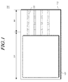
- FIG. 1 is a plan view of a flexible display device according to an embodiment when the display device is not bent
- a flexible display device 100 includes a flexible substrate 110, wiring 120, and a display layer or display panel 130.
- the flexible substrate 110 is a substrate that supports various elements of the flexible display device 100 and has softness.
- the flexible substrate 110 is named a soft substrate, a first soft substrate, or a flexible member.
- the flexible substrate 110 may be named a plastic film, a plastic substrate, or a first soft substrate.
- the flexible substrate 110 is formed in the shape of a rectangular parallelepiped, but is not limited thereto and can be formed in various shapes.
- the flexible substrate 110 is made of soft material, for example, is a film including one selected from a group of polyester-based polymer, silicone-based polymer, acrylic polymer, polyolefin-based polymer, and copolymer of them.
- the flexible substrate 110 includes one selected from a group of polyethylene terephthalate (PET), polybutylene terephthalate (PBT), polysilane, polysiloxane, polysilazane, polycarbosilane, polyacrylate, polymethacrylate, polymethylacrylate, polymethylmetacrylate, polyethylacrylate, polyethylmetacrylate, cyclic olefin copolymer (COC), cyclic olefin polymer (COP), polyethylene (PE), polypropylene (PP), polyimide (PI), polymethylmethacrylate (PMMA), polystyrene (PS), polyacetal (POM), polyetheretherketone (PEEK), polyester sulfone (PES
- the flexible substrate 110 includes a display area (DA) and a non-display area (NA).
- the display area (DA) of the flexible substrate is an area in which a real image is displayed and the non-display area of the flexible substrate 110 is an area in which an image is not displayed.
- the non-display area (NA) of the flexible substrate 110 is an area extending from the display area (DA) of the flexible substrate 110.
- the non-display area (NA) of the flexible substrate 110 is an area extending from a side of the display area (DA) of the flexible substrate 110.
- the display area (DA) of the flexible substrate 110 is formed in a polygonal shape and the non-display area (NA) of the flexible substrate 110 extends from a side of the display area (DA) of the flexible substrate 110.
- the non-display area (NA) of the flexible substrate 110 which extends from a side of the display area (DA) of the flexible substrate 110 is illustrated in FIG. 1 for the convenience of description, but is not limited thereto. Therefore, the non-display area (NA) of the flexible substrate 110 may extend from a plurality of sides of the display area (DA) of the flexible substrate 110.
- the non-display area (NA) of the flexible substrate 110 is disposed in peripheral areas or edge areas of the display area (DA) of the flexible substrate 110 and various circuits for displaying image are arranged therein, the non-display area (NA) is named a peripheral area, a peripheral circuit area, an edge area, or a bezel area.
- the display layer 130 is disposed in the entire area or a portion area of the display area (DA) of the flexible substrate 110.
- the display layer 130 is an element for displaying a real image, and is also named an image display layer. There is no limitation as long as the display layer 130 is an element capable of displaying an image.
- the display layer 130 is an organic light-emitting display layer that includes an organic light-emitting device to display an image via an organic light-emitting layer and a thin film transistor to drive the organic light-emitting device.
- the thin film transistor includes an active layer, a gate insulating layer, a gate electrode, an intermediate insulating layer disposed on the gate electrode and the active layer, and a source electrode and a drain electrode electrically connected to the active layer.
- the organic light-emitting device includes a first electrode electrically connected to anyone of the source electrode and the drain electrode, an organic light-emitting layer disposed on the first electrode, and a second electrode disposed on the organic light-emitting layer.
- NA non-display area
- the elements disposed in the non-display area (NA) of the flexible substrate 110 include various drive integrated circuits such as a gate drive integrated circuit or a data drive integrated circuit, drive circuit section, and the like.
- the various drive integrated circuit and the drive circuit section are mounted in the flexible substrate 110 in the manner of a Gate in Panel (GIP), or are connected to the flexible substrate 110 in the manner of a Tape Carrier Package (TCP) or a Chip On Film (COF).
- GIP Gate in Panel
- TCP Tape Carrier Package
- COF Chip On Film
- the wiring 120 is disposed on the flexible substrate 110.
- the wiring 120 electrically connects the display layer 130 disposed in the display area (DA) of the flexible substrate 110 to the drive circuit section or the gate drive integrated circuit, and the data drive integrated circuit disposed in the non-display area (NA) of the flexible substrate 110 for signal transmission.
- the wiring 120 is formed of a conductive material, and is formed of a conductive material with excellent softness in order to minimize the occurrence of a crack when bending the flexible substrate.
- the wiring 120 is formed of a conductive material with excellent softness such as gold (Au), silver (Ag), aluminum (Al), and the like.
- constituents of the wiring 120 are not limited thereto, and the wiring 120 is formed of one of various conductive materials used in manufacturing the display layer 130, and specifically, may be formed of molybdenum (Mo), chrome (Cr), titanium (Ti), nickel (Ni), neodymium (Nd), copper (Cu), an alloy of silver (Ag) and magnesium (Mg), or the like that is one of various conductive materials used in manufacturing the display layer 130.
- the wiring 120 is formed in a multilayered structure including the various conductive materials described above. For example, the wiring 120 is formed in a three-layered structure of titanium (Ti) / aluminum (Al) / titanium (Ti), but is not limited thereto.
- At least a portion area of the non-display area (NA) of the flexible substrate 110 is formed in a shape that is bent in a bending direction.
- the non-display area (NA) of the flexible substrate 110 having a shape that is bent in the bending direction is named a bend area.
- the non-display area (NA) of the flexible substrate 110 is not an area in which an image is displayed, the non-display area (NA) does not have to be acknowledged in the upper surface of the flexible substrate 110 and at least a portion area of the non-display area (NA) is bent.
- FIG. 1 illustrates a case that the entire non-display area (NA) of the flexible substrate 110 is the bend area.
- the bend area is not limited thereto and only a portion area of the non-display area (NA) of the flexible substrate 110 may be the bend area.
- FIG. 1 illustrates a case that the entire non-display area (NA) of the flexible substrate 110 is the bend area.
- the bend area is not limited thereto and only a portion area of the non-display area (NA) of the flexible substrate 110 may be the bend area.
- the non-display area (NA) of the flexible substrate 110 is slightly narrower than the display area (DA) of the flexible substrate 110, but the non-display area (NA) of the flexible substrate 110 may be greatly narrower than the display area (DA) of the flexible substrate 110.
- the bend area which is at least a portion area of the non-display area (NA) of the flexible substrate 110, is formed in a shape that is bent in the bending direction.
- the bending direction is a lateral direction of the flexible substrate 110, and a case that the bend area being at least a portion area of the non-display area (NA) of the flexible substrate 110 is bent in the lateral direction of the flexible substrate 110 is illustrated.
- FIG. 2 is a cross section of a flexible display device under a bent condition.
- FIG. 3 is a cross section of a flexible substrate, a display layer, and a connection member of a drive integrated circuit of the flexible display device of FIG. 2 under a non-bent condition.
- a flexible display device 200 is bent in a shape that at least a portion area of a non-display area (NA) of a flexible substrate 210 is bent in a bending direction.
- NA non-display area
- a display layer 230 is disposed on a display area (DA) of a surface 210a of the flexible substrate 210.
- a cover coat 240 is disposed on the non-display area (NA) of the surface 210a of the flexible substrate 210 to prevent moisture permeation or crack occurrence.
- the cover coat 240 is disposed in the bend area described with reference to FIG. 1 .
- a drive integrated circuit connection member 250 is connected to the non-display area (NA) of the surface 210a of the flexible substrate 210.
- Various drive integrated circuits such as a gate drive integrated or a data drive integrated circuit, a drive circuit section, and the like are mounted on the drive integrated circuit connection member 250.
- the drive integrated circuit connection member 250 is at least one of the tape carrier package (TCP) and the chip on film (COF).
- the wiring 120 illustrated in FIG. 1 is disposed on the flexible substrate 210, but is not shown for the convenience of description.
- the cover coat 240 is disposed between the display layer 230 and the drive integrated circuit connection member 250, and covers a portion 230a of the display layer 230 and a portion 250a of the drive integrated circuit connection member 250.
- a polarizing layer 232 is disposed on the display layer 230, but is not limited thereto.
- a cover coat 236 is disposed on the polarizing layer 232, and the polarizing layer 232 and the cover coat 236 are bonded together by an adhesive layer 234.
- At least a portion area of the non-display area (NA) of the flexible substrate 210 and the cover coat 240 is bent in a shape that is bent in the bending direction.
- a first back plate 260a that is disposed to correspond to the display layer 230 and a second back plate 260bthat is disposed to correspond to the drive integrated circuit connection member 250 and is positioned under the first back plate 260a when the flexible substrate 210 is bent in the bending direction are disposed.
- a supporting member 270 is positioned to be in contact with a bend area of the other surface 210b of the flexible substrate 210 between the first back plate 260a and the second back plate 260b in the vertical direction to support the flexible substrate 210.
- a head 270a of the supporting member 270 has a semicircular shape with a shorter radius than that of the bent flexible substrate 210. Therefore, the head 270a of the supporting member 270 is in surface to surface contact with the bend area of the other surface 210b of the flexible substrate 210.
- the flexible substrate 210 When the flexible substrate 210 is bent in the bending direction, tension is caused in the flexible substrate 210. In the flexible substrate 210, the most powerful tension is caused in a direction equal to the bending direction, and crack occurs in itself or due to external impact, or the occurred crack propagates to the display layer 230. Such crack of the flexible substrate 210 may cause breaking of the wiring (not shown) disposed in the non-display area (NA). In bending, the wiring (not shown) is positioned in an intermediate surface by using the cover coat 240 so that the crack of the wiring can be prevented
- a bend of the display layer 230 is needed to reduce the bezel area, and the cover coat 240 is formed to prevent moisture permeation and crack occurrence in the bend area. It is possible to prevent crack occurrence by contacting the head 270a of the supporting member 270 to the bend area of the other surface 210b of the flexible substrate 210 in order to support the bend area.
- the head 270a of the supporting member 270 when configured to be a semicircular shape having a radius equal to a radius of the bend area of the flexible substrate 210 in the flexible display device 200 described above, the head 270a of the supporting member 270 is entirely in surface to surface contact with the other surface 210b of the flexible substrate 210 so that stability and curvature reliability of the supporting member 270 can be improved. Therefore, it is possible to improve the effect that the supporting member 270 prevents wiring crack in the entire bend area of the other surface 210b of the flexible substrate 210.
- the supporting member 270 does not include the head 270a being entirely in surface to surface contact with the bend area of the other surface 210b of the flexible substrate 210, and thus occurrence of wiring crack caused by an impact with the supporting member 270 can be removed.
- the cover coat 240 is formed by using various materials through various processes. For example, as illustrate in FIG. 5 , the cover coat 240 is formed by coating organic resin (for example, acrylic resin) through the jetting process. The display layer 230 and the wiring (not shown) are formed in the display area (DA) and the non-display area (NA) of the flexible substrate 210, respectively. Then, while the drive integrate circuit connection member 250 in which a drive integrated circuit is mounted is connected to the flexible substrate 210, the cover coat 240 is formed by coating the organic resin 410 between an end 230a of the display layer 230 and an end of the drive integrated circuit connection member 250 using a jetting apparatus 240, and performing a hardening process by using ultraviolet (UV) or the like.
- UV ultraviolet
- FIGS. 6a and 6b are diagrams of illustrating a case that the cover coat is normally formed and a case that the cover coat is abnormally formed based on a process error when the cover coat is formed by using the jetting process of FIG. 5
- the organic resin 410 for the cover coat 240 is to be coated on the end 230a of the display layer 230 and is not to be coated on the polarizing layer 232 on the display layer 230 or the adhesive layer 234 to bond the polarizing layer 232 and the cover coat 236 together.
- the organic resin 410 may be coated on the polarizing layer 232 on the display layer 230 or the adhesive layer 234 to bond the polarizing layer 232 and the cover coat 236 together.
- an air gap may occur between the adhesive layer 234 and the cover coat 236 due to a portion of the cover coat 240 protruding over the adhesive layer 234 when the cover coat 236 and the polarizing layer 232 are bonded by using the adhesive layer 234. Bubbles occur between the adhesive layer 234 and the cover coat 236, and thus adhesion failure of the cover coat 236 or panel failure may be caused.
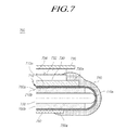
- FIG. 7 is a cross section of the flexible display device according to an embodiment.
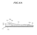
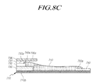
- FIG. 8 is a cross section of a flexible substrate, a display layer, and a drive integrated circuit connection member of the flexible display device of FIG. 7 under a non-bent condition.
- a flexible display device 700 includes a flexible substrate 710 having a display area (DA) and a non-display area (NA) extending from the display area (DA), a display layer 730 disposed in the display area (DA) of the flexible substrate 710, a polarizing layer 732 disposed on the display layer 730, and a cover coat 740 disposed in the non-display area (NA) of the flexible substrate 710.
- DA display area
- NA non-display area
- the flexible display device 700 includes a first back plate 760a that is disposed on a surface 710b of the flexible substrate 710 to correspond to the display layer 730, and a second back plate 7 60b that is disposed on the surface 710b of the flexible substrate 710 and separated from the first back plate 760a.
- the flexible display device 700 includes a supporting member 770 positioned between the first back plate 760a and the second back plate 760b in the vertical direction and is separated from the flexible substrate 710.
- the head 770a of the supporting member 770 is a semicircular shape bigger than the body and has the same radium as a radius of the bent flexible substrate 710, and the head 770a of the supporting member 770 is entirely in surface to surface contact with a bend area of the other surface 710b of the flexible substrate 710, so that stability and curvature reliability of the supporting member 770 can be improved.
- the head 770a of the supporting member 770 may have the same shape as the heads described in FIGS. 2 to 4c .
- the supporting member 770 may not have the head 770a as described FIG. 4c .
- wiring (not shown) is disposed on the flexible substrate 710.
- the wiring electrically connects the display layer 730 disposed in the display area (DA) of the flexible substrate 710 to the drive circuit section or the gate drive integrated circuit, and the data drive integrated circuit disposed in the non-display area (NA) of the flexible substrate 710 for signal transmission.
- the wiring is formed of a conductive material, and is formed of a conductive material with excellent softness in order to minimize the occurrence of a crack when bending the flexible substrate 710.
- a drive integrated circuit connection member 750 is connected to the non-display area (NA) of the flexible substrate 710, and the cover coat 740 is positioned between the display layer 730 and the drive integrated circuit connection member 750. As illustrated in FIG. 7 , the cover coat 740 is positioned between the display layer 730 and the drive integrated circuit connection member 750. As described above, the drive integrated circuit connection member 750 is one of the tape carrier package (TCP) or the chip on film (COF).
- TCP tape carrier package
- COF chip on film
- At least a portion area of the non-display area (NA) of the flexible substrate 710 is positioned to have a shape that is bent in a bending direction.
- the flexible display device 700 includes the cover coat 740 that is disposed in the non-display area (NA) of a surface 710a of the flexible substrate 710 and positioned to have a shape bent in the bending direction.
- the cover coat 740 is also positioned to have a shape bent in the bending direction similarly to the at least a portion area of the non-display area (NA) of the flexible substrate 710.
- An intermediate surface is disposed between the at least a portion area of the non-display area (NA) of the flexible substrate 710 positioned to have a shape that is bent in a bending direction and the cover coat 740.
- the wiring positioned in the non-display area (NA) of the flexible substrate 710 configures the intermediate surface by dint of the flexible substrate 710 and the cover coat 740.
- a polarizing layer 732, a cover coat 736, and a first adhesive layer 734 bonding the polarizing layer 732 and the cover coat 736 together are positioned on the display layer 730.
- an organic resin is coated from the drive integrated circuit connection member 750 of the non-display area (NA) of the flexible substrate 710 to the display layer 730 and an end 732a of the polarizing layer 732 of the display area (DA) of the flexible substrate 710 by using the jetting process of FIG. 5 , and then is hardened.
- an end 740a of the cover coat 740 is disposed on the end 730a of the display layer 730 and the end 732a of the polarizing layer 732.
- the first adhesive layer 734 and the cover coat 736 are directly bonded together on the polarizing layer 732.
- a bend area of the flexible substrate 710 is bent so that the flexible display device 700 illustrated in FIG. 7 can be obtained.
- the cover coat 740 is formed by using the jetting process before bonding the first adhesive layer 734 to the polarizing layer 732.
- the end 740a of the cover coat 740 is positioned between the polarizing layer 732 and the first adhesive layer 734 on the polarizing layer 732.
- an air gap does not occur between the first adhesive layer 734 and the cover coat 736, it is possible to minimize or prevent adhesive layer failure of the cover coat 736 or panel failure caused by the air gap occurring between the first adhesive layer 734 and the cover coat 736.
- the flexible display device 700 includes a barrier layer 738 between the display layer 730 and the polarizing layer 732.
- the end 740a of the cover coat 740 is positioned between the polarizing layer 732 and the first adhesive layer 734 on the barrier layer 738 and the polarizing layer 732.
- the end 740a of the cover coat 740 is positioned between the polarizing layer 732 and the first adhesive layer 734 on an end 738a of the barrier layer 738 and the end 732a of the polarizing layer 732.
- the flexible display device 700 includes a second adhesive layer 739 between the polarizing layer 732 and the display layer 730 when not including the barrier layer 738.
- the flexible display device 700 includes the second adhesive layer 739 between the polarizing layer 732 and the barrier layer 738.
- the end 740a of the cover coat 740 is positioned between the polarizing layer 732 and the first adhesive layer 734, or is positioned between the second adhesive layer 739 and the polarizing layer 732.
- the end 740a of the cover coat 740 is positioned between the display layer 730 and the second adhesive layer 739 on the display layer 730. Specifically, the end 740a of the cover coat 740 is positioned between the display layer 730 and the second adhesive layer 739 on the end 730a of the display layer 730.
- the end 740a of the cover coat 740 is positioned between the second adhesive layer 739 and the polarizing layer 732 on the second adhesive layer 739. Specifically, the end 740a of the cover coat 740 is positioned between the second adhesive layer 739 and the polarizing layer 732 on the end 739a of the second adhesive layer 739.
- the end 740a of the cover coat 740 is positioned between the barrier layer 738 and the second adhesive layer 739 on the barrier layer 738. Specifically, the end 740a of the cover coat 740 is positioned between the barrier layer 738 and the second adhesive layer 739 on the end 738a of the barrier layer 738.
- the end 740a of the cover coat 740 is positioned between the second adhesive layer 739 and the polarizing layer 732 on the second adhesive layer 739. Specifically, the end 740a of the cover coat 740 is positioned between the second adhesive layer 739 and the polarizing layer 732 on the end 739a of the second adhesive layer 739.
- the cover coat 740 is positioned in the non-display area (NA) of the surface 710a of the flexible substrate 710, and the end 740a is disposed under the polarizing layer 732 or on the polarizing layer 732. That is, the end 740a of the cover coat 740 is positioned on at least one of the display layer 730, the barrier layer 738, the second adhesive layer 739, the polarizing layer 732, and the first adhesive layer 734.
- NA non-display area
- any one of the display layer 730, the barrier layer 734, the second adhesive layer 739, the polarizing layer 732, and a first adhesive layer 734 is positioned on the display layer 730 as an element on which the end 740a of the cover coat 740 is positioned, and then the organic resin 410 is coated through the jetting process of FIG. 5 .
- the cover coat 740 is positioned in the non-display area (NA) of the surface 710a of the flexible substrate 710 and the end 740a is positioned under the polarizing layer 732 or on the polarizing layer 732.
- NA non-display area
- the drive integrated circuit connection member 750 is connected to the non-display area (NA) of the surface 710a of the flexible substrate 710, and the cover coat 740 can cover an end of the drive integrated circuit connection member 750.
- NA non-display area
- the first back plate 760a is disposed to correspond the display layer 730
- the second back plate 760b is disposed to correspond the drive integrated circuit connection member 750 and is positioned under the first back plate 760a when the flexible substrate 710 is bent in the bending direction.
- a supporting member 770 is positioned between the first backplate 760a and the secondbackplate 760b in the vertical direction.
- the flexible display device 700 illustrated in FIG. 7 includes at least one of the first back plate 760a, the second back plate 760b, and the supporting member 770 under a bent condition, but is not limited thereto.
- the support structure of the other surface 710b of the flexible substrate 710 is variously implemented.
Landscapes
- Engineering & Computer Science (AREA)
- Microelectronics & Electronic Packaging (AREA)
- Physics & Mathematics (AREA)
- Geometry (AREA)
- Devices For Indicating Variable Information By Combining Individual Elements (AREA)
- Electroluminescent Light Sources (AREA)
- Optics & Photonics (AREA)
Abstract
Description
- This application claims priority from Korean Patent Application No.
10-2015-0114888 filed on August 13, 2015 - The present disclosure relates to a flexible display device.
- An organic light emitting diodes(OLED) display device, a plasma display panel (PDP) display device, or the like emitting light by themselves, a liquid crystal display device requiring a separate light source, or the like has been used in a monitor of a computer, a TV, a cellular phone, and the like.
- Recently, a flexible display device, which is manufactured by forming a display panel, wiring, and the like on a flexible substrate such as a plastic of a flexible material so that an image can be displayed under a bent condition like paper, has been in the spotlight as a next generation display device.
- The flexible display device has been variously applied to not only a monitor of a computer and a TV but also a personal mobile device, and a flexible display device having reduced volume and weight in spite of a wide display area has been studied.
- In such flexible display device, crack occurs in the flexible substrate or the wiring based on various causes when bending the display device. This crack occurring in the flexible substrate or the wiring may cause a failure of the flexible display device.
- According to an aspect of the present invention, there is provided a flexible display device which may include a flexible substrate, a display layer (or display panel), at least one additional layer, and a cover coat.
- The flexible substrate may have a display area and a non-display area extending from the display area. The display layer may be disposed in a display area of a first surface of the flexible substrate. The at least one additional layer may be disposed on the display layer. The cover coat may be disposed on a non-display area of the first surface of the flexible substrate, and an end of the cover coat may be disposed between two neighboring layers of the layers disposed on the display area. At least a portion of the non-display area of the flexible substrate and the cover coat are bendable in a bending direction.
- The at least one additional layer on the display layer may comprise a first adhesive layer on a polarizing layer or a second adhesive layer under a polarizing layer, and the end of the cover coat is positioned between the polarizing layer and the first adhesive layer, or between the second adhesive layer and the polarizing layer.
- The flexible display device may comprise an adhesive layer and a barrier layer (or barrier film) . The adhesive layer may be positioned between the display layer and the polarizing layer. The barrier layer may be positioned between the display layer and the second adhesive layer. In this case, the end of the cover coat may be positioned between the barrier layer and the second adhesive layer on the barrier layer.
- The flexible display device may further comprise a first adhesive layer on the polarizing layer, a second adhesive layer may be positioned between the display layer and the polarizing layer, and a barrier layer between the display layer and the second adhesive layer. In this case, the end of the cover coat may be positioned between the polarizing layer and the first adhesive layer on the barrier layer and the polarizing layer.
- A drive integrated circuit connection member may be connected to the non-display area of the surface of the flexible substrate. And the cover coat may be covering an end of the drive integrated circuit connection member.
- The flexible display device may further comprise a first back plate and a second back plate. The first back plate may be disposed on a second surface of the flexible substrate to correspond to the display layer. The second back plate may be disposed to correspond to the drive integrated circuit connection member. The second back plate may be positioned under the first back plate when the flexible substrate is bent in the bending direction.
- The drive integrated circuit connection member is at least one of a tape carrier package (TCP) and a chip on film (COF).
- The flexible display device may further comprise a supporting member. The supporting member may be positioned between the first back plate and the second back plate in a vertical direction.
- According to the aspects of the present invention, crack can be prevented from occurring in a flexible substrate or wiring when bending a flexible display device.
- According to the aspects of the present invention, it is possible to prevent or minimize a failure in a flexible display device.
- The above and other aspects, features and other advantages of the present invention will be more clearly understood from the following detailed description taken in conjunction with the accompanying drawings, in which:
-
FIG. 1 is a plan view of a flexible display device in a non-bent condition; -
FIG. 2 is a cross section of a flexible display device under a bent condition; -
FIG. 3 is a cross section of a flexible substrate, a display layer, and a connection member of a drive integrated circuit of the flexible display device ofFIG. 2 under a non-bent condition; -
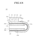
FIGS. 4a to 4c are cross-sections of modified examples of the flexible display device ofFIG. 2 ; -
FIG. 5 is a diagram illustrating a process of manufacturing a cover coat ofFIG. 2 ; -
FIGS. 6a and6b are diagrams illustrating a case that the cover coat is normally formed and a case that the cover coat is abnormally formed based on a process error when the cover coat is formed by using a jetting process ofFIG. 5 ; -
FIG. 7 is a cross section of the flexible display device according to an embodiment; -
FIG. 8 is a cross section of a flexible substrate, a display layer, and a drive integrated circuit connection member of the flexible display device ofFIG. 7 under a non-bent condition; and -
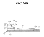
FIGS. 9 to 11b are cross sections of modified examples of the flexible display device ofFIG. 7 . - Hereinafter, some exemplary embodiments of the present invention will be described in detail with reference to the accompanying drawings. In adding reference numerals to components throughout the drawings, like reference numerals may designate like components even though components are shown in different drawings. Further, in explaining the exemplary embodiments of the present invention, a detailed explanation of well-known components or functions may be omitted to avoid unnecessarily obscuring the subject matter of the present invention.
- Further, in describing components of the present invention, terms such as first, second, A, B, (a), (b), etc. can be used. These terms are used only to differentiate the components from other components. Therefore, the nature, order, sequence, or number of the corresponding components is not limited by these terms. It is to be understood that when one element is referred to as being "connected to" or "coupled to" another element, it may be directly connected to or directly coupled to another element, connected to or coupled to another element, having still another element "intervening" therebetween, or "connected to" or "coupled to" another element via still another element.
- In this specification, a flexible display device means a display device with softness, and may be used to have a similar meaning to a bendable display device, a rollable display device, an unbreakable display device, a foldable display device, or the like. In this specification, a flexible OLED display device is an example of various flexible display devices.
- In this specification, the display device has a display area and a non-display area. The display area is an area in which an image or the like is displayed, and the non-display area is an area in which an image is not displayed like a bezel.
-
FIG. 1 is a plan view of a flexible display device according to an embodiment when the display device is not bent - Referring to
FIG. 1 , aflexible display device 100 includes aflexible substrate 110,wiring 120, and a display layer ordisplay panel 130. - The
flexible substrate 110 is a substrate that supports various elements of theflexible display device 100 and has softness. Theflexible substrate 110 is named a soft substrate, a first soft substrate, or a flexible member. When being made of plastic, theflexible substrate 110 may be named a plastic film, a plastic substrate, or a first soft substrate. Theflexible substrate 110 is formed in the shape of a rectangular parallelepiped, but is not limited thereto and can be formed in various shapes. - The
flexible substrate 110 is made of soft material, for example, is a film including one selected from a group of polyester-based polymer, silicone-based polymer, acrylic polymer, polyolefin-based polymer, and copolymer of them. Specifically, theflexible substrate 110 includes one selected from a group of polyethylene terephthalate (PET), polybutylene terephthalate (PBT), polysilane, polysiloxane, polysilazane, polycarbosilane, polyacrylate, polymethacrylate, polymethylacrylate, polymethylmetacrylate, polyethylacrylate, polyethylmetacrylate, cyclic olefin copolymer (COC), cyclic olefin polymer (COP), polyethylene (PE), polypropylene (PP), polyimide (PI), polymethylmethacrylate (PMMA), polystyrene (PS), polyacetal (POM), polyetheretherketone (PEEK), polyester sulfone (PES), polytetrafluoroethylene (PTFE), polyvinyl chloride (PVC), polycarbonate (PC), polyvinylidene fluoride (PVDF), perfluoroalkyl polymers (PFA), a styrene acrylic polymer nitro rilko (SAN), and a combination of them. In some embodiments, when theflexible display device 100 is implemented by a transparent flexible display device, theflexible substrate 110 is formed of a transparent soft material. - The
flexible substrate 110 includes a display area (DA) and a non-display area (NA). The display area (DA) of the flexible substrate is an area in which a real image is displayed and the non-display area of theflexible substrate 110 is an area in which an image is not displayed. - The non-display area (NA) of the
flexible substrate 110 is an area extending from the display area (DA) of theflexible substrate 110. The non-display area (NA) of theflexible substrate 110 is an area extending from a side of the display area (DA) of theflexible substrate 110. For example, when the display area (DA) of theflexible substrate 110 is formed in a polygonal shape and the non-display area (NA) of theflexible substrate 110 extends from a side of the display area (DA) of theflexible substrate 110. The non-display area (NA) of theflexible substrate 110 which extends from a side of the display area (DA) of theflexible substrate 110 is illustrated inFIG. 1 for the convenience of description, but is not limited thereto. Therefore, the non-display area (NA) of theflexible substrate 110 may extend from a plurality of sides of the display area (DA) of theflexible substrate 110. - As the non-display area (NA) of the
flexible substrate 110 is disposed in peripheral areas or edge areas of the display area (DA) of theflexible substrate 110 and various circuits for displaying image are arranged therein, the non-display area (NA) is named a peripheral area, a peripheral circuit area, an edge area, or a bezel area. - The
display layer 130 is disposed in the entire area or a portion area of the display area (DA) of theflexible substrate 110. Thedisplay layer 130 is an element for displaying a real image, and is also named an image display layer. There is no limitation as long as thedisplay layer 130 is an element capable of displaying an image. In this specification, thedisplay layer 130 is an organic light-emitting display layer that includes an organic light-emitting device to display an image via an organic light-emitting layer and a thin film transistor to drive the organic light-emitting device. - The thin film transistor includes an active layer, a gate insulating layer, a gate electrode, an intermediate insulating layer disposed on the gate electrode and the active layer, and a source electrode and a drain electrode electrically connected to the active layer. The organic light-emitting device includes a first electrode electrically connected to anyone of the source electrode and the drain electrode, an organic light-emitting layer disposed on the first electrode, and a second electrode disposed on the organic light-emitting layer.
- Various elements not displaying an image are disposed in the non-display area (NA) of the
flexible substrate 110 - The elements disposed in the non-display area (NA) of the
flexible substrate 110 include various drive integrated circuits such as a gate drive integrated circuit or a data drive integrated circuit, drive circuit section, and the like. Here, the various drive integrated circuit and the drive circuit section are mounted in theflexible substrate 110 in the manner of a Gate in Panel (GIP), or are connected to theflexible substrate 110 in the manner of a Tape Carrier Package (TCP) or a Chip On Film (COF). - The
wiring 120 is disposed on theflexible substrate 110. Thewiring 120 electrically connects thedisplay layer 130 disposed in the display area (DA) of theflexible substrate 110 to the drive circuit section or the gate drive integrated circuit, and the data drive integrated circuit disposed in the non-display area (NA) of theflexible substrate 110 for signal transmission. - The
wiring 120 is formed of a conductive material, and is formed of a conductive material with excellent softness in order to minimize the occurrence of a crack when bending the flexible substrate. For example, thewiring 120 is formed of a conductive material with excellent softness such as gold (Au), silver (Ag), aluminum (Al), and the like. However, constituents of thewiring 120 are not limited thereto, and thewiring 120 is formed of one of various conductive materials used in manufacturing thedisplay layer 130, and specifically, may be formed of molybdenum (Mo), chrome (Cr), titanium (Ti), nickel (Ni), neodymium (Nd), copper (Cu), an alloy of silver (Ag) and magnesium (Mg), or the like that is one of various conductive materials used in manufacturing thedisplay layer 130. Thewiring 120 is formed in a multilayered structure including the various conductive materials described above. For example, thewiring 120 is formed in a three-layered structure of titanium (Ti) / aluminum (Al) / titanium (Ti), but is not limited thereto. - At least a portion area of the non-display area (NA) of the
flexible substrate 110 is formed in a shape that is bent in a bending direction. - Here, at least the portion area of the non-display area (NA) of the
flexible substrate 110 having a shape that is bent in the bending direction is named a bend area. As the non-display area (NA) of theflexible substrate 110 is not an area in which an image is displayed, the non-display area (NA) does not have to be acknowledged in the upper surface of theflexible substrate 110 and at least a portion area of the non-display area (NA) is bent. For the convenience of description,FIG. 1 illustrates a case that the entire non-display area (NA) of theflexible substrate 110 is the bend area. However, the bend area is not limited thereto and only a portion area of the non-display area (NA) of theflexible substrate 110 may be the bend area. For the convenience of description,FIG. 1 illustrates a case that the non-display area (NA) of theflexible substrate 110 is slightly narrower than the display area (DA) of theflexible substrate 110, but the non-display area (NA) of theflexible substrate 110 may be greatly narrower than the display area (DA) of theflexible substrate 110. - The bend area, which is at least a portion area of the non-display area (NA) of the
flexible substrate 110, is formed in a shape that is bent in the bending direction. InFIG. 1 , the bending direction is a lateral direction of theflexible substrate 110, and a case that the bend area being at least a portion area of the non-display area (NA) of theflexible substrate 110 is bent in the lateral direction of theflexible substrate 110 is illustrated. - Hereinafter, various flexible display devices under a bent condition will be described with reference to the accompanying drawings.
-
FIG. 2 is a cross section of a flexible display device under a bent condition.FIG. 3 is a cross section of a flexible substrate, a display layer, and a connection member of a drive integrated circuit of the flexible display device ofFIG. 2 under a non-bent condition. - Referring to
FIGS. 2 and3 , aflexible display device 200 is bent in a shape that at least a portion area of a non-display area (NA) of aflexible substrate 210 is bent in a bending direction. - A
display layer 230 is disposed on a display area (DA) of asurface 210a of theflexible substrate 210. - A
cover coat 240 is disposed on the non-display area (NA) of thesurface 210a of theflexible substrate 210 to prevent moisture permeation or crack occurrence. Thecover coat 240 is disposed in the bend area described with reference toFIG. 1 . - A drive integrated
circuit connection member 250 is connected to the non-display area (NA) of thesurface 210a of theflexible substrate 210. Various drive integrated circuits such as a gate drive integrated or a data drive integrated circuit, a drive circuit section, and the like are mounted on the drive integratedcircuit connection member 250. The drive integratedcircuit connection member 250 is at least one of the tape carrier package (TCP) and the chip on film (COF). - The
wiring 120 illustrated inFIG. 1 is disposed on theflexible substrate 210, but is not shown for the convenience of description. - The
cover coat 240 is disposed between thedisplay layer 230 and the drive integratedcircuit connection member 250, and covers aportion 230a of thedisplay layer 230 and aportion 250a of the drive integratedcircuit connection member 250. - A
polarizing layer 232 is disposed on thedisplay layer 230, but is not limited thereto. Acover coat 236 is disposed on thepolarizing layer 232, and thepolarizing layer 232 and thecover coat 236 are bonded together by anadhesive layer 234. - At least a portion area of the non-display area (NA) of the
flexible substrate 210 and thecover coat 240 is bent in a shape that is bent in the bending direction. - On the
other surface 210b of theflexible substrate 210, afirst back plate 260a that is disposed to correspond to thedisplay layer 230 and a second back plate 260bthat is disposed to correspond to the drive integratedcircuit connection member 250 and is positioned under thefirst back plate 260a when theflexible substrate 210 is bent in the bending direction are disposed. - A supporting
member 270 is positioned to be in contact with a bend area of theother surface 210b of theflexible substrate 210 between thefirst back plate 260a and thesecond back plate 260b in the vertical direction to support theflexible substrate 210. Ahead 270a of the supportingmember 270 has a semicircular shape with a shorter radius than that of the bentflexible substrate 210. Therefore, thehead 270a of the supportingmember 270 is in surface to surface contact with the bend area of theother surface 210b of theflexible substrate 210. - When the
flexible substrate 210 is bent in the bending direction, tension is caused in theflexible substrate 210. In theflexible substrate 210, the most powerful tension is caused in a direction equal to the bending direction, and crack occurs in itself or due to external impact, or the occurred crack propagates to thedisplay layer 230. Such crack of theflexible substrate 210 may cause breaking of the wiring (not shown) disposed in the non-display area (NA). In bending, the wiring (not shown) is positioned in an intermediate surface by using thecover coat 240 so that the crack of the wiring can be prevented - In
flexible display device 200, a bend of thedisplay layer 230 is needed to reduce the bezel area, and thecover coat 240 is formed to prevent moisture permeation and crack occurrence in the bend area. It is possible to prevent crack occurrence by contacting thehead 270a of the supportingmember 270 to the bend area of theother surface 210b of theflexible substrate 210 in order to support the bend area. - As illustrated in
FIGS. 4a and4b , when thehead 270a of the supportingmember 270 is configured to be a semicircular shape having a radius equal to a radius of the bend area of theflexible substrate 210 in theflexible display device 200 described above, thehead 270a of the supportingmember 270 is entirely in surface to surface contact with theother surface 210b of theflexible substrate 210 so that stability and curvature reliability of the supportingmember 270 can be improved. Therefore, it is possible to improve the effect that the supportingmember 270 prevents wiring crack in the entire bend area of theother surface 210b of theflexible substrate 210. - As illustrated in
FIG. 4c , the supportingmember 270 does not include thehead 270a being entirely in surface to surface contact with the bend area of theother surface 210b of theflexible substrate 210, and thus occurrence of wiring crack caused by an impact with the supportingmember 270 can be removed. - The
cover coat 240 is formed by using various materials through various processes. For example, as illustrate inFIG. 5 , thecover coat 240 is formed by coating organic resin (for example, acrylic resin) through the jetting process. Thedisplay layer 230 and the wiring (not shown) are formed in the display area (DA) and the non-display area (NA) of theflexible substrate 210, respectively. Then, while the drive integratecircuit connection member 250 in which a drive integrated circuit is mounted is connected to theflexible substrate 210, thecover coat 240 is formed by coating theorganic resin 410 between anend 230a of thedisplay layer 230 and an end of the drive integratedcircuit connection member 250 using ajetting apparatus 240, and performing a hardening process by using ultraviolet (UV) or the like. -
FIGS. 6a and6b are diagrams of illustrating a case that the cover coat is normally formed and a case that the cover coat is abnormally formed based on a process error when the cover coat is formed by using the jetting process ofFIG. 5 - As illustrate in
FIG. 6a , when thecover coat 240 is formed through the jetting process, as described above, theorganic resin 410 for thecover coat 240 is to be coated on theend 230a of thedisplay layer 230 and is not to be coated on thepolarizing layer 232 on thedisplay layer 230 or theadhesive layer 234 to bond thepolarizing layer 232 and thecover coat 236 together. As illustrated inFIG. 6b , due to a process error of the jetting process, theorganic resin 410 may be coated on thepolarizing layer 232 on thedisplay layer 230 or theadhesive layer 234 to bond thepolarizing layer 232 and thecover coat 236 together. If theorganic resin 410 is coated on theadhesive layer 234 to bond thepolarizing layer 232 and thecover coat 236 together due to the process error and is hardened, an air gap may occur between theadhesive layer 234 and thecover coat 236 due to a portion of thecover coat 240 protruding over theadhesive layer 234 when thecover coat 236 and thepolarizing layer 232 are bonded by using theadhesive layer 234. Bubbles occur between theadhesive layer 234 and thecover coat 236, and thus adhesion failure of thecover coat 236 or panel failure may be caused. - Hereinafter, embodiments of a flexible display device, in which adhesion failure of a cover or panel failure can be improved although a cover coat is formed in a flexible substrate by using the jetting process, will be described with reference to the accompanying drawings.
-
FIG. 7 is a cross section of the flexible display device according to an embodiment.FIG. 8 is a cross section of a flexible substrate, a display layer, and a drive integrated circuit connection member of the flexible display device ofFIG. 7 under a non-bent condition. - Referring to
FIGS. 7 and8 , aflexible display device 700 according to an embodiment includes aflexible substrate 710 having a display area (DA) and a non-display area (NA) extending from the display area (DA), adisplay layer 730 disposed in the display area (DA) of theflexible substrate 710, apolarizing layer 732 disposed on thedisplay layer 730, and acover coat 740 disposed in the non-display area (NA) of theflexible substrate 710. - The
flexible display device 700 includes afirst back plate 760a that is disposed on asurface 710b of theflexible substrate 710 to correspond to thedisplay layer 730, and a second back plate 7 60b that is disposed on thesurface 710b of theflexible substrate 710 and separated from thefirst back plate 760a. - The
flexible display device 700 includes a supportingmember 770 positioned between thefirst back plate 760a and thesecond back plate 760b in the vertical direction and is separated from theflexible substrate 710. As illustrated inFIG. 7 , thehead 770a of the supportingmember 770 is a semicircular shape bigger than the body and has the same radium as a radius of the bentflexible substrate 710, and thehead 770a of the supportingmember 770 is entirely in surface to surface contact with a bend area of theother surface 710b of theflexible substrate 710, so that stability and curvature reliability of the supportingmember 770 can be improved. Here, thehead 770a of the supportingmember 770 may have the same shape as the heads described inFIGS. 2 to 4c . The supportingmember 770 may not have thehead 770a as describedFIG. 4c . - As illustrated in
FIG. 1 , wiring (not shown) is disposed on theflexible substrate 710. The wiring electrically connects thedisplay layer 730 disposed in the display area (DA) of theflexible substrate 710 to the drive circuit section or the gate drive integrated circuit, and the data drive integrated circuit disposed in the non-display area (NA) of theflexible substrate 710 for signal transmission. The wiring is formed of a conductive material, and is formed of a conductive material with excellent softness in order to minimize the occurrence of a crack when bending theflexible substrate 710. - A drive integrated
circuit connection member 750 is connected to the non-display area (NA) of theflexible substrate 710, and thecover coat 740 is positioned between thedisplay layer 730 and the drive integratedcircuit connection member 750. As illustrated inFIG. 7 , thecover coat 740 is positioned between thedisplay layer 730 and the drive integratedcircuit connection member 750. As described above, the drive integratedcircuit connection member 750 is one of the tape carrier package (TCP) or the chip on film (COF). - At least a portion area of the non-display area (NA) of the
flexible substrate 710 is positioned to have a shape that is bent in a bending direction. - The
flexible display device 700 includes thecover coat 740 that is disposed in the non-display area (NA) of asurface 710a of theflexible substrate 710 and positioned to have a shape bent in the bending direction. Thecover coat 740 is also positioned to have a shape bent in the bending direction similarly to the at least a portion area of the non-display area (NA) of theflexible substrate 710. - An intermediate surface is disposed between the at least a portion area of the non-display area (NA) of the
flexible substrate 710 positioned to have a shape that is bent in a bending direction and thecover coat 740. Specifically, the wiring positioned in the non-display area (NA) of theflexible substrate 710 configures the intermediate surface by dint of theflexible substrate 710 and thecover coat 740. When the at least partial area of the non-display area (NA) of theflexible substrate 710 and thecover coat 740 are bent in the bending direction, aposition in which strains of at least a portion area of the non-display area (NA) of theflexible substrate 710 and thecover coat 740 caused by the bending become zero is named the intermediate surface. - A
polarizing layer 732, acover coat 736, and a firstadhesive layer 734 bonding thepolarizing layer 732 and thecover coat 736 together are positioned on thedisplay layer 730. - As illustrated in
FIG. 8a , in a state that thedisplay layer 730 and thepolarizing layer 732 are positioned in the display area (DA) of theflexible substrate 710 and the drive integratedcircuit connection member 750 is connected to the non-display area (NA) of theflexible substrate 710, an organic resin is coated from the drive integratedcircuit connection member 750 of the non-display area (NA) of theflexible substrate 710 to thedisplay layer 730 and anend 732a of thepolarizing layer 732 of the display area (DA) of theflexible substrate 710 by using the jetting process ofFIG. 5 , and then is hardened. - Next, as illustrated in
FIGS 8b and8c , anend 740a of thecover coat 740 is disposed on theend 730a of thedisplay layer 730 and theend 732a of thepolarizing layer 732. The firstadhesive layer 734 and thecover coat 736 are directly bonded together on thepolarizing layer 732. Then, in a state that a support structure of thefirst back plate 760a, thesecond back plate 760b, and the supportingmember 770 is positioned on theother surface 710b of theflexible substrate 710, a bend area of theflexible substrate 710 is bent so that theflexible display device 700 illustrated inFIG. 7 can be obtained. - In the
flexible display device 700 illustrated inFIG. 8a , thecover coat 740 is formed by using the jetting process before bonding the firstadhesive layer 734 to thepolarizing layer 732. Thus, when theorganic resin 410 is coated over thepolarizing layer 732 due to the process error, theend 740a of thecover coat 740 is positioned between thepolarizing layer 732 and the firstadhesive layer 734 on thepolarizing layer 732. As an air gap does not occur between the firstadhesive layer 734 and thecover coat 736, it is possible to minimize or prevent adhesive layer failure of thecover coat 736 or panel failure caused by the air gap occurring between the firstadhesive layer 734 and thecover coat 736. - As illustrated in
FIG. 9 , theflexible display device 700 includes abarrier layer 738 between thedisplay layer 730 and thepolarizing layer 732. When theflexible display device 700 includes thebarrier layer 738, theend 740a of thecover coat 740 is positioned between thepolarizing layer 732 and the firstadhesive layer 734 on thebarrier layer 738 and thepolarizing layer 732. Specifically, theend 740a of thecover coat 740 is positioned between thepolarizing layer 732 and the firstadhesive layer 734 on anend 738a of thebarrier layer 738 and theend 732a of thepolarizing layer 732. - As illustrated in
FIGS. 10a and10b , theflexible display device 700 includes a secondadhesive layer 739 between thepolarizing layer 732 and thedisplay layer 730 when not including thebarrier layer 738. Theflexible display device 700 includes the secondadhesive layer 739 between thepolarizing layer 732 and thebarrier layer 738. - The
end 740a of thecover coat 740 is positioned between thepolarizing layer 732 and the firstadhesive layer 734, or is positioned between the secondadhesive layer 739 and thepolarizing layer 732. - As illustrated in
FIG. 10a , when thebarrier layer 738 is not included, theend 740a of thecover coat 740 is positioned between thedisplay layer 730 and the secondadhesive layer 739 on thedisplay layer 730. Specifically, theend 740a of thecover coat 740 is positioned between thedisplay layer 730 and the secondadhesive layer 739 on theend 730a of thedisplay layer 730. - As illustrated in
FIG. 10b , when thebarrier layer 738 is not included, theend 740a of thecover coat 740 is positioned between the secondadhesive layer 739 and thepolarizing layer 732 on the secondadhesive layer 739. Specifically, theend 740a of thecover coat 740 is positioned between the secondadhesive layer 739 and thepolarizing layer 732 on theend 739a of the secondadhesive layer 739. - As illustrated in
FIG. 11a , when thebarrier layer 738 is included, theend 740a of thecover coat 740 is positioned between thebarrier layer 738 and the secondadhesive layer 739 on thebarrier layer 738. Specifically, theend 740a of thecover coat 740 is positioned between thebarrier layer 738 and the secondadhesive layer 739 on theend 738a of thebarrier layer 738. - As illustrated in
FIG. 11b , when thebarrier layer 738 is included, theend 740a of thecover coat 740 is positioned between the secondadhesive layer 739 and thepolarizing layer 732 on the secondadhesive layer 739. Specifically, theend 740a of thecover coat 740 is positioned between the secondadhesive layer 739 and thepolarizing layer 732 on theend 739a of the secondadhesive layer 739. - In the embodiments described above, the
cover coat 740 is positioned in the non-display area (NA) of thesurface 710a of theflexible substrate 710, and theend 740a is disposed under thepolarizing layer 732 or on thepolarizing layer 732. That is, theend 740a of thecover coat 740 is positioned on at least one of thedisplay layer 730, thebarrier layer 738, the secondadhesive layer 739, thepolarizing layer 732, and the firstadhesive layer 734. In forming thecover coat 740 by coating theorganic resin 410 through the jetting process ofFIG. 5 , any one of thedisplay layer 730, thebarrier layer 734, the secondadhesive layer 739, thepolarizing layer 732, and a firstadhesive layer 734 is positioned on thedisplay layer 730 as an element on which theend 740a of thecover coat 740 is positioned, and then theorganic resin 410 is coated through the jetting process ofFIG. 5 . - In the embodiments described above, the
cover coat 740 is positioned in the non-display area (NA) of thesurface 710a of theflexible substrate 710 and theend 740a is positioned under thepolarizing layer 732 or on thepolarizing layer 732. As a result, an air gap does not occur between theadhesive layer 734 and thecover coat 736, and it is possible to minimize or prevent adhesion failure of thecover coat 736 or panel failure by dint of the air gap occurring between theadhesive layer 734 and thecover coat 740. - As illustrated in
FIGS. 7 to 11b , the drive integratedcircuit connection member 750 is connected to the non-display area (NA) of thesurface 710a of theflexible substrate 710, and thecover coat 740 can cover an end of the drive integratedcircuit connection member 750. - As described above, in the
other surface 710b of theflexible substrate 710, thefirst back plate 760a is disposed to correspond thedisplay layer 730, and thesecond back plate 760b is disposed to correspond the drive integratedcircuit connection member 750 and is positioned under thefirst back plate 760a when theflexible substrate 710 is bent in the bending direction. A supportingmember 770 is positioned between thefirst backplate 760a and the secondbackplate 760b in the vertical direction. - Referring to
FIGS. 2 and4a to 4c , theflexible display device 700 illustrated inFIG. 7 includes at least one of thefirst back plate 760a, thesecond back plate 760b, and the supportingmember 770 under a bent condition, but is not limited thereto. The support structure of theother surface 710b of theflexible substrate 710 is variously implemented. - According to the embodiments described above, it is possible to prevent an occurrence of the crack in the flexible substrate or wiring when the flexible display device is bent.
- According to the embodiments described above, it is possible to prevent or minimize failure in the flexible display device.
- The foregoing description and the accompanying drawings are provided only to illustrate the technical conception of the present invention, but it will be understood by a person having ordinary skill in the art that various modifications and changes such as combinations, separations, substitutions, and alterations of the components may be made without departing from the scope of the present invention. Therefore, the exemplary embodiments of the present invention are provided for illustrative purposes only but not intended to limit the technical concept of the present invention. The scope of the technical concept of the present invention is not limited thereto . The protective scope of the present invention shouldbe construed based on the following claims, and all the technical concepts in the equivalent scope thereof should be construed as falling within the scope of the present invention.
Claims (12)
- A flexible display device (100, 700), comprising:a flexible substrate (110, 710) including a display area (DA) and a non-display area (NA);a display layer (130, 730) on the display area of the flexible substrate, the display layer being disposed on a first surface (710a) of the flexible substrate;at least one additional layer (732, 734, 738, 739) on the display layer (130, 730); anda cover coat (740) on the non-display area of the flexible substrate, the cover coat being disposed on the first surface (710a) of the flexible substrate;wherein at least a portion of the non-display area (NA) of the flexible substrate (710) and the cover coat (740) are bendable in a bending direction; andwherein an end (740a) of the cover coat (740) is positioned between two neighboring ones of the layers (730, 732, 734, 738, 739) disposed on the display area (DA).
- The flexible display device (700) according to claim 1,
wherein the at least one additional layer on the display layer comprises a first adhesive layer (734) on a polarizing layer (732) or a second adhesive layer (739) under a polarizing layer (732), and
wherein the end (740a) of the cover coat (740) is positioned between the polarizing layer (732) and the first adhesive layer (734), or between the second adhesive layer (739) and the polarizing layer (732), respectively. - The flexible display device (700) according to claim 2, further comprising a barrier layer (738) between the display layer (730) and the polarizing layer (732).
- The flexible display device (700) according to claim 1, wherein
the at least one additional layer on the display layer comprises an adhesive layer (739) on the display layer (730), and
the end (740a) of the cover coat (740) is positioned between the display layer (730) and the adhesive layer (739). - The flexible display device (700) according to claim 1, wherein
the at least one additional layer on the display layer comprises a barrier layer (738) on the display layer (730), and
the end (740a) of the cover coat (740) is positioned between the display layer (730) and the barrier layer (738). - The flexible display device (700) according to claim 1,
wherein the at least one additional layer on the display layer comprises a barrier layer (738) on the display layer (730), and an adhesive layer (739) on the barrier layer (738), and
wherein the end (740a) of the cover coat (740) is positioned between the barrier layer (738) and the adhesive layer (739). - The flexible display device (700) according to any one of claims 1 to 6, wherein the at least one additional layer (732, 734, 738, 739) in the display area (DA) comprises a cover layer (736).
- The flexible display device (700) according to claim 1, wherein
the at least one additional layer (732, 734, 738, 739) in the display area (DA) comprises a polarizing layer (732) and a cover layer (736), and
an adhesive layer (734) is disposed between the polarizing layer (732) and the cover layer (736). - The flexible display device (700) according to any one of claims 1 to 8, wherein
a drive integrated circuit connection member (750) is connected to the non-display area (NA) of the surface (710a) of the flexible substrate (710), and
the cover coat (740) covers an end (750a) of the drive integrated circuit connection member (750). - The flexible display device (700) according to any one of claims 1 to 9, further comprising:a first back plate (760a) which is disposed on a second surface (710b) of the flexible substrate (710) to correspond to the display layer (730), anda second back plate (760b) which is disposed on the second surface (710b) of the flexible substrate (710) to correspond to a drive integrated circuit connection member (750) and which is positioned under the first back plate in a constellation in which the flexible substrate has been bent in the bending direction.
- The flexible display device (700) according to claim 10, wherein
the drive integrated circuit connection member (750) is at least one of a tape carrier package (TCP) and a chip on film (COF). - The flexible display device (700) according to claim 10 or 11, further comprising:a supporting member (770) which is positioned between the first back plate (760a) and the second back plate (760b) in a constellation in which the flexible substrate has been bent in the bend
Priority Applications (1)
| Application Number | Priority Date | Filing Date | Title |
|---|---|---|---|
| EP22163535.2A EP4036998B1 (en) | 2015-08-13 | 2016-06-24 | Flexible display device |
Applications Claiming Priority (1)
| Application Number | Priority Date | Filing Date | Title |
|---|---|---|---|
| KR1020150114888A KR102550857B1 (en) | 2015-08-13 | 2015-08-13 | Flexible display device |
Related Child Applications (2)
| Application Number | Title | Priority Date | Filing Date |
|---|---|---|---|
| EP22163535.2A Division-Into EP4036998B1 (en) | 2015-08-13 | 2016-06-24 | Flexible display device |
| EP22163535.2A Division EP4036998B1 (en) | 2015-08-13 | 2016-06-24 | Flexible display device |
Publications (2)
| Publication Number | Publication Date |
|---|---|
| EP3133656A1 true EP3133656A1 (en) | 2017-02-22 |
| EP3133656B1 EP3133656B1 (en) | 2022-05-11 |
Family
ID=56740766
Family Applications (2)
| Application Number | Title | Priority Date | Filing Date |
|---|---|---|---|
| EP22163535.2A Active EP4036998B1 (en) | 2015-08-13 | 2016-06-24 | Flexible display device |
| EP16176231.5A Active EP3133656B1 (en) | 2015-08-13 | 2016-06-24 | Flexible display device |
Family Applications Before (1)
| Application Number | Title | Priority Date | Filing Date |
|---|---|---|---|
| EP22163535.2A Active EP4036998B1 (en) | 2015-08-13 | 2016-06-24 | Flexible display device |
Country Status (4)
| Country | Link |
|---|---|
| US (2) | US10153457B2 (en) |
| EP (2) | EP4036998B1 (en) |
| KR (4) | KR102550857B1 (en) |
| CN (2) | CN108054189B (en) |
Cited By (1)
| Publication number | Priority date | Publication date | Assignee | Title |
|---|---|---|---|---|
| EP4147275A4 (en) * | 2020-09-09 | 2023-06-21 | BOE Technology Group Co., Ltd. | DISPLAY DEVICE |
Families Citing this family (92)
| Publication number | Priority date | Publication date | Assignee | Title |
|---|---|---|---|---|
| JP6474337B2 (en) * | 2015-08-27 | 2019-02-27 | 株式会社ジャパンディスプレイ | Display device and manufacturing method thereof |
| JP6727843B2 (en) * | 2016-02-25 | 2020-07-22 | 株式会社ジャパンディスプレイ | Display device |
| KR102449220B1 (en) * | 2016-03-21 | 2022-09-30 | 삼성디스플레이 주식회사 | display device |
| JP6695727B2 (en) * | 2016-04-08 | 2020-05-20 | 株式会社ジャパンディスプレイ | Display device |
| CN206179906U (en) * | 2016-12-01 | 2017-05-17 | 京东方科技集团股份有限公司 | Display device |
| KR102695129B1 (en) * | 2016-12-22 | 2024-08-13 | 엘지디스플레이 주식회사 | Organic light emitting display device |
| KR102329830B1 (en) * | 2017-01-10 | 2021-11-23 | 삼성디스플레이 주식회사 | Organic light emitting display device |
| CN106910429B (en) * | 2017-03-08 | 2019-05-14 | 京东方科技集团股份有限公司 | A flexible module and method of making the same |
| CN107146527B (en) * | 2017-04-27 | 2020-01-03 | 上海天马微电子有限公司 | Flexible display screen and flexible display device |
| JP6860666B2 (en) * | 2017-06-28 | 2021-04-21 | 日東電工株式会社 | Polarizer |
| JP2019012098A (en) * | 2017-06-29 | 2019-01-24 | 株式会社ジャパンディスプレイ | Display device |
| KR102342822B1 (en) | 2017-07-14 | 2021-12-23 | 삼성디스플레이 주식회사 | Display device |
| JP7030444B2 (en) * | 2017-08-07 | 2022-03-07 | 株式会社ジャパンディスプレイ | Display device |
| US20190051858A1 (en) * | 2017-08-10 | 2019-02-14 | Japan Display Inc. | Display device |
| JP6564909B2 (en) * | 2017-08-10 | 2019-08-21 | 株式会社ジャパンディスプレイ | Display device |
| KR102481818B1 (en) | 2017-08-22 | 2022-12-28 | 삼성디스플레이 주식회사 | Electronic component, electric device including the same |
| KR102430099B1 (en) * | 2017-09-29 | 2022-08-04 | 엘지디스플레이 주식회사 | Electroluminescence display device |
| KR102476190B1 (en) * | 2017-10-17 | 2022-12-08 | 엘지디스플레이 주식회사 | Flexible electroluminescent display device |
| CN107768413B (en) * | 2017-10-26 | 2020-12-01 | 京东方科技集团股份有限公司 | A flexible display substrate, a display device and a manufacturing method thereof |
| WO2019104657A1 (en) * | 2017-11-30 | 2019-06-06 | 深圳市柔宇科技有限公司 | Flexible display device, fabrication method for flexible display device and electronic device |
| JP7029948B2 (en) * | 2017-12-04 | 2022-03-04 | 株式会社ジャパンディスプレイ | Display device |
| KR102471758B1 (en) * | 2017-12-11 | 2022-11-29 | 삼성디스플레이 주식회사 | Display device |
| US10910592B2 (en) * | 2017-12-22 | 2021-02-02 | Lg Display Co., Ltd. | Flexible electroluminescent display device |
| KR102581944B1 (en) * | 2017-12-22 | 2023-09-22 | 삼성디스플레이 주식회사 | Display device |
| KR102507096B1 (en) * | 2018-01-05 | 2023-03-08 | 삼성디스플레이 주식회사 | Flexible display device |
| KR20190087694A (en) * | 2018-01-15 | 2019-07-25 | 삼성디스플레이 주식회사 | Display device and method for manufacturing the display device |
| CN110161733A (en) * | 2018-02-14 | 2019-08-23 | 群创光电股份有限公司 | Show equipment and its manufacturing method |
| KR102451778B1 (en) * | 2018-02-20 | 2022-10-06 | 삼성디스플레이 주식회사 | Display device |
| KR102543688B1 (en) * | 2018-04-02 | 2023-06-14 | 삼성디스플레이 주식회사 | Display device and manufacturing method of display device |
| CN108735785B (en) * | 2018-05-21 | 2020-05-19 | 武汉华星光电半导体显示技术有限公司 | OLED display panel and manufacturing method thereof |
| CN108735101B (en) | 2018-05-28 | 2020-01-31 | 京东方科技集团股份有限公司 | Flexible display device |
| CN108735103B (en) | 2018-05-31 | 2019-09-17 | 京东方科技集团股份有限公司 | A kind of display backboard |
| KR102601569B1 (en) * | 2018-06-08 | 2023-11-15 | 삼성디스플레이 주식회사 | Display device |
| KR102591639B1 (en) | 2018-06-12 | 2023-10-19 | 삼성디스플레이 주식회사 | Display device |
| KR102622861B1 (en) * | 2018-06-22 | 2024-01-10 | 삼성디스플레이 주식회사 | Flexible substrate and display apparatus including the same |
| CN108878483A (en) * | 2018-06-22 | 2018-11-23 | 武汉华星光电半导体显示技术有限公司 | Display panel and electronic equipment |
| KR102662203B1 (en) * | 2018-07-17 | 2024-04-30 | 삼성디스플레이 주식회사 | Display device |
| CN108682307B (en) * | 2018-07-18 | 2024-06-25 | 昆山国显光电有限公司 | Display panel and display device |
| KR102554557B1 (en) * | 2018-08-01 | 2023-07-11 | 엘지디스플레이 주식회사 | Light emitting display device with integrated touch screen |
| CN110943066A (en) * | 2018-09-21 | 2020-03-31 | 联华电子股份有限公司 | Semiconductor structure with high-resistance chip and bonding method of high-resistance chip |
| CN109377877A (en) * | 2018-09-26 | 2019-02-22 | 武汉华星光电半导体显示技术有限公司 | Display module and electronic device |
| KR102706503B1 (en) * | 2018-10-08 | 2024-09-12 | 엘지디스플레이 주식회사 | Display Unit |
| KR102677937B1 (en) * | 2018-10-11 | 2024-06-24 | 삼성디스플레이 주식회사 | Display device and manufacturing method thereof |
| KR102712302B1 (en) * | 2018-10-15 | 2024-10-04 | 삼성디스플레이 주식회사 | Display device |
| JP7100559B2 (en) * | 2018-10-25 | 2022-07-13 | 株式会社ジャパンディスプレイ | Display device |
| US12101426B1 (en) * | 2018-11-13 | 2024-09-24 | Apple Inc. | Electronic devices having vertical image transport layers |
| KR102656855B1 (en) * | 2018-11-15 | 2024-04-11 | 엘지디스플레이 주식회사 | Flexible Electroluminescent Display Apparatus |
| KR102617455B1 (en) * | 2018-11-20 | 2023-12-26 | 주식회사 루멘스 | flexible LED display module and manufacturing method therof |
| KR102562204B1 (en) * | 2018-12-13 | 2023-07-31 | 엘지디스플레이 주식회사 | Flexible display module and electronic device comprising the same |
| CN109445154A (en) * | 2018-12-17 | 2019-03-08 | 武汉华星光电半导体显示技术有限公司 | A kind of display panel |
| CN109541834B (en) * | 2018-12-29 | 2021-11-02 | 厦门天马微电子有限公司 | Display panel and display device |
| KR102769277B1 (en) * | 2019-02-13 | 2025-02-21 | 삼성디스플레이 주식회사 | Display device and manufacturing method thereof |
| KR102697819B1 (en) * | 2019-02-27 | 2024-08-26 | 삼성디스플레이 주식회사 | Display device |
| CN109901319A (en) * | 2019-03-29 | 2019-06-18 | 武汉华星光电技术有限公司 | Display panels and electronic equipment |
| KR102688018B1 (en) * | 2019-05-13 | 2024-07-25 | 삼성디스플레이 주식회사 | Nput sensing unit, display device including same, and method for manufacturing same |
| KR102827635B1 (en) | 2019-07-24 | 2025-07-04 | 삼성디스플레이 주식회사 | Display apparatus and method of manufacturing the same |
| US11605314B2 (en) * | 2019-07-26 | 2023-03-14 | Au Optronics Corporation | Flexible display device and manufacturing method thereof |
| KR102137093B1 (en) | 2019-08-05 | 2020-07-23 | 삼성전기주식회사 | Antenna module and electronic device including thereof |
| CN110491883B (en) * | 2019-08-14 | 2022-04-29 | 京东方科技集团股份有限公司 | Display panel, method for making the same, and display device |
| US11121333B2 (en) * | 2019-09-16 | 2021-09-14 | Wuhan China Star Optoelectronics Semiconductor Display Technology Co., Ltd. | OLED display panel and method for fabricating same |
| KR20210049326A (en) * | 2019-10-25 | 2021-05-06 | 엘지디스플레이 주식회사 | Flexible display device |
| KR102752716B1 (en) * | 2019-10-28 | 2025-01-08 | 엘지디스플레이 주식회사 | Flexible display device |
| KR102688752B1 (en) * | 2019-11-05 | 2024-07-26 | 삼성디스플레이 주식회사 | Cover window and method for manufacturing the same and display device comrpising cover window |
| CN111129340A (en) * | 2019-12-05 | 2020-05-08 | 武汉华星光电半导体显示技术有限公司 | Display panel and display device |
| CN111146358A (en) * | 2019-12-26 | 2020-05-12 | 武汉华星光电半导体显示技术有限公司 | Flexible cover plate and flexible display device |
| KR102860969B1 (en) | 2019-12-27 | 2025-09-16 | 엘지디스플레이 주식회사 | Flexible display device |
| KR102823806B1 (en) * | 2019-12-31 | 2025-06-20 | 엘지디스플레이 주식회사 | Display apparatus |
| US11686883B2 (en) * | 2020-02-14 | 2023-06-27 | Samsung Display Co., Ltd. | Display device having bendable area |
| KR102947571B1 (en) * | 2020-02-14 | 2026-04-06 | 삼성디스플레이 주식회사 | Display device |
| CN113644181B (en) | 2020-05-11 | 2024-04-16 | 京东方科技集团股份有限公司 | Light-emitting substrate and method for manufacturing the same, and display device |
| CN111724678A (en) * | 2020-06-08 | 2020-09-29 | 武汉华星光电半导体显示技术有限公司 | Flexible display device and flexible display equipment |
| WO2022025671A1 (en) * | 2020-07-29 | 2022-02-03 | 삼성전자 주식회사 | Electronic device including rollable or slidable display |
| CN112002740A (en) * | 2020-08-10 | 2020-11-27 | 深圳市华星光电半导体显示技术有限公司 | Substrate, separation method thereof and display panel |
| US11889647B2 (en) | 2020-08-19 | 2024-01-30 | Apple Inc. | Display panel bend reinforcement |
| CN114467132B (en) | 2020-09-09 | 2024-04-09 | 京东方科技集团股份有限公司 | Display device and method of manufacturing the same |
| CN112420792B (en) * | 2020-11-17 | 2024-01-26 | 武汉华星光电半导体显示技术有限公司 | Display panel, binding method and display device thereof |
| KR102824666B1 (en) * | 2020-12-29 | 2025-06-23 | 엘지디스플레이 주식회사 | Display device |
| CN113314033A (en) * | 2021-05-20 | 2021-08-27 | 武汉华星光电半导体显示技术有限公司 | Display device |
| CN113328056B (en) * | 2021-05-31 | 2022-09-02 | 武汉天马微电子有限公司 | A display panel and display device |
| CN113470529A (en) * | 2021-06-30 | 2021-10-01 | 云谷(固安)科技有限公司 | Display device |
| KR20230012123A (en) * | 2021-07-14 | 2023-01-26 | 삼성디스플레이 주식회사 | Display device |
| KR102890701B1 (en) * | 2021-07-15 | 2025-11-25 | 삼성디스플레이 주식회사 | Display device |
| CN113555408B (en) * | 2021-07-21 | 2024-05-24 | 京东方科技集团股份有限公司 | Display device, display module and manufacturing method thereof |
| KR20230035172A (en) | 2021-09-03 | 2023-03-13 | 삼성디스플레이 주식회사 | Folable display device |
| KR20230047794A (en) * | 2021-10-01 | 2023-04-10 | 엘지디스플레이 주식회사 | Flexible display device |
| KR102877605B1 (en) | 2021-10-28 | 2025-10-28 | 삼성디스플레이 주식회사 | Display device having the same |
| KR20230103702A (en) * | 2021-12-31 | 2023-07-07 | 엘지디스플레이 주식회사 | Light emitting display apparatus |
| CN115631686B (en) * | 2022-09-27 | 2025-04-11 | 厦门天马显示科技有限公司 | Flexible display panel and display device |
| KR20240093102A (en) * | 2022-12-15 | 2024-06-24 | 엘지디스플레이 주식회사 | Display apparatus and method for manufacturing the same |
| KR20240104455A (en) * | 2022-12-28 | 2024-07-05 | 엘지디스플레이 주식회사 | Display apparatus and method of fabricating thereof |
| CN117475745A (en) * | 2023-05-31 | 2024-01-30 | 武汉华星光电半导体显示技术有限公司 | display module |
| CN120014936A (en) * | 2025-02-08 | 2025-05-16 | 厦门天马显示科技有限公司 | Display module, method for manufacturing display module, and display device |
Citations (4)
| Publication number | Priority date | Publication date | Assignee | Title |
|---|---|---|---|---|
| US20100293782A1 (en) * | 2009-05-21 | 2010-11-25 | Semiconductor Energy Laboratory Co., Ltd. | Method for manufacturing light-emitting device |
| US20130034685A1 (en) * | 2011-08-02 | 2013-02-07 | Cheol-Geun An | Display device and method for manufacturing the same |
| US20140021499A1 (en) * | 2012-07-19 | 2014-01-23 | Samsung Display Co., Ltd. | Flexible display apparatus and method of fabricating the same |
| US20150137098A1 (en) * | 2013-11-20 | 2015-05-21 | Panasonic Corporation | Display device and method for manufacturing the same |
Family Cites Families (14)
| Publication number | Priority date | Publication date | Assignee | Title |
|---|---|---|---|---|
| CA2316587C (en) * | 2000-08-14 | 2009-12-01 | Charles M. Schmeichel | Tonneau cover having rear bar lock |
| US7559847B2 (en) * | 2006-07-28 | 2009-07-14 | Clawson Custom Cues, Inc. | Cue stick |
| KR101436115B1 (en) * | 2007-04-27 | 2014-09-01 | 가부시키가이샤 한도오따이 에네루기 켄큐쇼 | Method of manufacturing semiconductor substrate and method of manufacturing semiconductor device |
| US8716932B2 (en) * | 2011-02-28 | 2014-05-06 | Apple Inc. | Displays with minimized borders |
| KR101615791B1 (en) * | 2012-11-14 | 2016-04-26 | 엘지디스플레이 주식회사 | None-Bezel Display Panel Having Edge Bending Structure |
| KR101796813B1 (en) * | 2013-02-01 | 2017-11-10 | 엘지디스플레이 주식회사 | Flexible organic light emitting display device and method for manufacturing the same |
| US9349969B2 (en) * | 2013-02-01 | 2016-05-24 | Lg Display Co., Ltd. | Electronic devices with flexible display and method for manufacturing the same |
| KR102222680B1 (en) * | 2013-02-01 | 2021-03-03 | 엘지디스플레이 주식회사 | Flexible display substrate, flexible organic light emitting display device and method for manufacturing the same |
| KR102035462B1 (en) * | 2013-03-27 | 2019-10-23 | 엘지디스플레이 주식회사 | Slit coater, method for driving the same, flexible display device using the same and method for fabricating of the same |
| KR102081650B1 (en) | 2013-04-10 | 2020-02-26 | 엘지디스플레이 주식회사 | Flexible display device and method of manufacturing the same |
| US20150013709A1 (en) * | 2013-07-12 | 2015-01-15 | Chris Scheurn | Devices And Methods For Contacting Keratinaceous Nails With Solutions |
| KR102077525B1 (en) | 2013-07-30 | 2020-02-14 | 엘지디스플레이 주식회사 | Display device and method of manufacturing the same |
| US9876064B2 (en) * | 2013-08-30 | 2018-01-23 | Lg Display Co., Ltd. | Flexible organic electroluminescent device and method for fabricating the same |
| CN104393014B (en) * | 2014-10-22 | 2017-09-26 | 京东方科技集团股份有限公司 | A kind of array base palte and preparation method thereof, flexible display panels and display device |
-
2015
- 2015-08-13 KR KR1020150114888A patent/KR102550857B1/en active Active
-
2016
- 2016-06-24 EP EP22163535.2A patent/EP4036998B1/en active Active
- 2016-06-24 EP EP16176231.5A patent/EP3133656B1/en active Active
- 2016-08-11 CN CN201711389175.6A patent/CN108054189B/en active Active
- 2016-08-11 CN CN201610658492.2A patent/CN106449699B/en active Active
- 2016-08-12 US US15/235,818 patent/US10153457B2/en active Active
-
2017
- 2017-12-21 US US15/851,427 patent/US10374194B2/en active Active
-
2023
- 2023-06-28 KR KR1020230083291A patent/KR102686324B1/en active Active
-
2024
- 2024-07-15 KR KR1020240092936A patent/KR102839087B1/en active Active
-
2025
- 2025-07-23 KR KR1020250099440A patent/KR20250119502A/en active Pending
Patent Citations (4)
| Publication number | Priority date | Publication date | Assignee | Title |
|---|---|---|---|---|
| US20100293782A1 (en) * | 2009-05-21 | 2010-11-25 | Semiconductor Energy Laboratory Co., Ltd. | Method for manufacturing light-emitting device |
| US20130034685A1 (en) * | 2011-08-02 | 2013-02-07 | Cheol-Geun An | Display device and method for manufacturing the same |
| US20140021499A1 (en) * | 2012-07-19 | 2014-01-23 | Samsung Display Co., Ltd. | Flexible display apparatus and method of fabricating the same |
| US20150137098A1 (en) * | 2013-11-20 | 2015-05-21 | Panasonic Corporation | Display device and method for manufacturing the same |
Cited By (1)
| Publication number | Priority date | Publication date | Assignee | Title |
|---|---|---|---|---|
| EP4147275A4 (en) * | 2020-09-09 | 2023-06-21 | BOE Technology Group Co., Ltd. | DISPLAY DEVICE |
Also Published As
| Publication number | Publication date |
|---|---|
| US20170047547A1 (en) | 2017-02-16 |
| CN108054189A (en) | 2018-05-18 |
| KR102550857B1 (en) | 2023-07-05 |
| US10153457B2 (en) | 2018-12-11 |
| US10374194B2 (en) | 2019-08-06 |
| KR102839087B1 (en) | 2025-07-28 |
| US20180114944A1 (en) | 2018-04-26 |
| KR20240113739A (en) | 2024-07-23 |
| KR20230106543A (en) | 2023-07-13 |
| EP3133656B1 (en) | 2022-05-11 |
| CN106449699A (en) | 2017-02-22 |
| KR102686324B1 (en) | 2024-07-19 |
| CN106449699B (en) | 2019-08-06 |
| KR20250119502A (en) | 2025-08-07 |
| CN108054189B (en) | 2022-03-04 |
| EP4036998B1 (en) | 2026-01-28 |
| EP4036998A1 (en) | 2022-08-03 |
| KR20170020674A (en) | 2017-02-23 |
Similar Documents
| Publication | Publication Date | Title |
|---|---|---|
| EP4036998B1 (en) | Flexible display device | |
| KR102402874B1 (en) | Flexible display device | |
| KR102902602B1 (en) | Flexible display apparatus | |
| US10658436B2 (en) | Organic light emitting display device to implement narrow bezel and thin thickness | |
| US10732674B2 (en) | Flexible display device having flexible display substrate curved around support substrate | |
| KR20260005149A (en) | Flexible display apparatus | |
| US10431769B2 (en) | Organic light emitting display device | |
| US20180183001A1 (en) | Organic Light Emitting Display Device | |
| KR20180003684A (en) | Flexible substrate, flexible display device and method for manufacturing the same | |
| KR102371301B1 (en) | Flexible display device | |
| KR101899831B1 (en) | Flexible display device | |
| US10868270B2 (en) | Display device | |
| CN220570916U (en) | Display apparatus | |
| KR20200066919A (en) | Organic light emitting display device | |
| CN103165624B (en) | Driving substrate, display device, planarizing method, and method of manufacturing driving substrate | |
| KR20260003457A (en) | Display device |
Legal Events
| Date | Code | Title | Description |
|---|---|---|---|
| PUAI | Public reference made under article 153(3) epc to a published international application that has entered the european phase |
Free format text: ORIGINAL CODE: 0009012 |
|
| STAA | Information on the status of an ep patent application or granted ep patent |
Free format text: STATUS: REQUEST FOR EXAMINATION WAS MADE |
|
| 17P | Request for examination filed |
Effective date: 20160624 |
|
| AK | Designated contracting states |
Kind code of ref document: A1 Designated state(s): AL AT BE BG CH CY CZ DE DK EE ES FI FR GB GR HR HU IE IS IT LI LT LU LV MC MK MT NL NO PL PT RO RS SE SI SK SM TR |
|
| AX | Request for extension of the european patent |
Extension state: BA ME |
|
| RBV | Designated contracting states (corrected) |
Designated state(s): AL AT BE BG CH CY CZ DE DK EE ES FI FR GB GR HR HU IE IS IT LI LT LU LV MC MK MT NL NO PL PT RO RS SE SI SK SM TR |
|
| R17P | Request for examination filed (corrected) |
Effective date: 20160624 |
|
| STAA | Information on the status of an ep patent application or granted ep patent |
Free format text: STATUS: EXAMINATION IS IN PROGRESS |
|
| 17Q | First examination report despatched |
Effective date: 20200114 |
|
| GRAP | Despatch of communication of intention to grant a patent |
Free format text: ORIGINAL CODE: EPIDOSNIGR1 |
|
| STAA | Information on the status of an ep patent application or granted ep patent |
Free format text: STATUS: GRANT OF PATENT IS INTENDED |
|
| INTG | Intention to grant announced |
Effective date: 20211209 |
|
| GRAS | Grant fee paid |
Free format text: ORIGINAL CODE: EPIDOSNIGR3 |
|
| GRAA | (expected) grant |
Free format text: ORIGINAL CODE: 0009210 |
|
| STAA | Information on the status of an ep patent application or granted ep patent |
Free format text: STATUS: THE PATENT HAS BEEN GRANTED |
|
| AK | Designated contracting states |
Kind code of ref document: B1 Designated state(s): AL AT BE BG CH CY CZ DE DK EE ES FI FR GB GR HR HU IE IS IT LI LT LU LV MC MK MT NL NO PL PT RO RS SE SI SK SM TR |
|
| REG | Reference to a national code |
Ref country code: GB Ref legal event code: FG4D |
|
| REG | Reference to a national code |
Ref country code: CH Ref legal event code: EP |
|
| REG | Reference to a national code |
Ref country code: AT Ref legal event code: REF Ref document number: 1492218 Country of ref document: AT Kind code of ref document: T Effective date: 20220515 |
|
| REG | Reference to a national code |
Ref country code: DE Ref legal event code: R096 Ref document number: 602016071971 Country of ref document: DE |
|
| REG | Reference to a national code |
Ref country code: IE Ref legal event code: FG4D |
|
| REG | Reference to a national code |
Ref country code: NL Ref legal event code: FP |
|
| REG | Reference to a national code |
Ref country code: LT Ref legal event code: MG9D |
|
| REG | Reference to a national code |
Ref country code: AT Ref legal event code: MK05 Ref document number: 1492218 Country of ref document: AT Kind code of ref document: T Effective date: 20220511 |
|
| PG25 | Lapsed in a contracting state [announced via postgrant information from national office to epo] |
Ref country code: SE Free format text: LAPSE BECAUSE OF FAILURE TO SUBMIT A TRANSLATION OF THE DESCRIPTION OR TO PAY THE FEE WITHIN THE PRESCRIBED TIME-LIMIT Effective date: 20220511 Ref country code: PT Free format text: LAPSE BECAUSE OF FAILURE TO SUBMIT A TRANSLATION OF THE DESCRIPTION OR TO PAY THE FEE WITHIN THE PRESCRIBED TIME-LIMIT Effective date: 20220912 Ref country code: NO Free format text: LAPSE BECAUSE OF FAILURE TO SUBMIT A TRANSLATION OF THE DESCRIPTION OR TO PAY THE FEE WITHIN THE PRESCRIBED TIME-LIMIT Effective date: 20220811 Ref country code: LT Free format text: LAPSE BECAUSE OF FAILURE TO SUBMIT A TRANSLATION OF THE DESCRIPTION OR TO PAY THE FEE WITHIN THE PRESCRIBED TIME-LIMIT Effective date: 20220511 Ref country code: HR Free format text: LAPSE BECAUSE OF FAILURE TO SUBMIT A TRANSLATION OF THE DESCRIPTION OR TO PAY THE FEE WITHIN THE PRESCRIBED TIME-LIMIT Effective date: 20220511 Ref country code: GR Free format text: LAPSE BECAUSE OF FAILURE TO SUBMIT A TRANSLATION OF THE DESCRIPTION OR TO PAY THE FEE WITHIN THE PRESCRIBED TIME-LIMIT Effective date: 20220812 Ref country code: FI Free format text: LAPSE BECAUSE OF FAILURE TO SUBMIT A TRANSLATION OF THE DESCRIPTION OR TO PAY THE FEE WITHIN THE PRESCRIBED TIME-LIMIT Effective date: 20220511 Ref country code: ES Free format text: LAPSE BECAUSE OF FAILURE TO SUBMIT A TRANSLATION OF THE DESCRIPTION OR TO PAY THE FEE WITHIN THE PRESCRIBED TIME-LIMIT Effective date: 20220511 Ref country code: BG Free format text: LAPSE BECAUSE OF FAILURE TO SUBMIT A TRANSLATION OF THE DESCRIPTION OR TO PAY THE FEE WITHIN THE PRESCRIBED TIME-LIMIT Effective date: 20220811 Ref country code: AT Free format text: LAPSE BECAUSE OF FAILURE TO SUBMIT A TRANSLATION OF THE DESCRIPTION OR TO PAY THE FEE WITHIN THE PRESCRIBED TIME-LIMIT Effective date: 20220511 |
|
| REG | Reference to a national code |
Ref country code: DE Ref legal event code: R079 Ref document number: 602016071971 Country of ref document: DE Free format text: PREVIOUS MAIN CLASS: H01L0051000000 Ipc: H10K0099000000 |
|
| PG25 | Lapsed in a contracting state [announced via postgrant information from national office to epo] |
Ref country code: RS Free format text: LAPSE BECAUSE OF FAILURE TO SUBMIT A TRANSLATION OF THE DESCRIPTION OR TO PAY THE FEE WITHIN THE PRESCRIBED TIME-LIMIT Effective date: 20220511 Ref country code: PL Free format text: LAPSE BECAUSE OF FAILURE TO SUBMIT A TRANSLATION OF THE DESCRIPTION OR TO PAY THE FEE WITHIN THE PRESCRIBED TIME-LIMIT Effective date: 20220511 Ref country code: LV Free format text: LAPSE BECAUSE OF FAILURE TO SUBMIT A TRANSLATION OF THE DESCRIPTION OR TO PAY THE FEE WITHIN THE PRESCRIBED TIME-LIMIT Effective date: 20220511 Ref country code: IS Free format text: LAPSE BECAUSE OF FAILURE TO SUBMIT A TRANSLATION OF THE DESCRIPTION OR TO PAY THE FEE WITHIN THE PRESCRIBED TIME-LIMIT Effective date: 20220911 |
|
| PG25 | Lapsed in a contracting state [announced via postgrant information from national office to epo] |
Ref country code: SM Free format text: LAPSE BECAUSE OF FAILURE TO SUBMIT A TRANSLATION OF THE DESCRIPTION OR TO PAY THE FEE WITHIN THE PRESCRIBED TIME-LIMIT Effective date: 20220511 Ref country code: SK Free format text: LAPSE BECAUSE OF FAILURE TO SUBMIT A TRANSLATION OF THE DESCRIPTION OR TO PAY THE FEE WITHIN THE PRESCRIBED TIME-LIMIT Effective date: 20220511 Ref country code: RO Free format text: LAPSE BECAUSE OF FAILURE TO SUBMIT A TRANSLATION OF THE DESCRIPTION OR TO PAY THE FEE WITHIN THE PRESCRIBED TIME-LIMIT Effective date: 20220511 Ref country code: EE Free format text: LAPSE BECAUSE OF FAILURE TO SUBMIT A TRANSLATION OF THE DESCRIPTION OR TO PAY THE FEE WITHIN THE PRESCRIBED TIME-LIMIT Effective date: 20220511 Ref country code: DK Free format text: LAPSE BECAUSE OF FAILURE TO SUBMIT A TRANSLATION OF THE DESCRIPTION OR TO PAY THE FEE WITHIN THE PRESCRIBED TIME-LIMIT Effective date: 20220511 Ref country code: CZ Free format text: LAPSE BECAUSE OF FAILURE TO SUBMIT A TRANSLATION OF THE DESCRIPTION OR TO PAY THE FEE WITHIN THE PRESCRIBED TIME-LIMIT Effective date: 20220511 |
|
| REG | Reference to a national code |
Ref country code: CH Ref legal event code: PL |
|
| REG | Reference to a national code |
Ref country code: DE Ref legal event code: R097 Ref document number: 602016071971 Country of ref document: DE |
|
| REG | Reference to a national code |
Ref country code: BE Ref legal event code: MM Effective date: 20220630 |
|
| PG25 | Lapsed in a contracting state [announced via postgrant information from national office to epo] |
Ref country code: MC Free format text: LAPSE BECAUSE OF FAILURE TO SUBMIT A TRANSLATION OF THE DESCRIPTION OR TO PAY THE FEE WITHIN THE PRESCRIBED TIME-LIMIT Effective date: 20220511 |
|
| PLBE | No opposition filed within time limit |
Free format text: ORIGINAL CODE: 0009261 |
|
| STAA | Information on the status of an ep patent application or granted ep patent |
Free format text: STATUS: NO OPPOSITION FILED WITHIN TIME LIMIT |
|
| PG25 | Lapsed in a contracting state [announced via postgrant information from national office to epo] |
Ref country code: AL Free format text: LAPSE BECAUSE OF FAILURE TO SUBMIT A TRANSLATION OF THE DESCRIPTION OR TO PAY THE FEE WITHIN THE PRESCRIBED TIME-LIMIT Effective date: 20220511 |
|
| 26N | No opposition filed |
Effective date: 20230214 |
|
| PG25 | Lapsed in a contracting state [announced via postgrant information from national office to epo] |
Ref country code: LU Free format text: LAPSE BECAUSE OF NON-PAYMENT OF DUE FEES Effective date: 20220624 Ref country code: LI Free format text: LAPSE BECAUSE OF NON-PAYMENT OF DUE FEES Effective date: 20220630 Ref country code: IE Free format text: LAPSE BECAUSE OF NON-PAYMENT OF DUE FEES Effective date: 20220624 Ref country code: CH Free format text: LAPSE BECAUSE OF NON-PAYMENT OF DUE FEES Effective date: 20220630 |
|
| PG25 | Lapsed in a contracting state [announced via postgrant information from national office to epo] |
Ref country code: SI Free format text: LAPSE BECAUSE OF FAILURE TO SUBMIT A TRANSLATION OF THE DESCRIPTION OR TO PAY THE FEE WITHIN THE PRESCRIBED TIME-LIMIT Effective date: 20220511 Ref country code: BE Free format text: LAPSE BECAUSE OF NON-PAYMENT OF DUE FEES Effective date: 20220630 |
|
| PG25 | Lapsed in a contracting state [announced via postgrant information from national office to epo] |
Ref country code: IT Free format text: LAPSE BECAUSE OF FAILURE TO SUBMIT A TRANSLATION OF THE DESCRIPTION OR TO PAY THE FEE WITHIN THE PRESCRIBED TIME-LIMIT Effective date: 20220511 |
|
| PG25 | Lapsed in a contracting state [announced via postgrant information from national office to epo] |
Ref country code: HU Free format text: LAPSE BECAUSE OF FAILURE TO SUBMIT A TRANSLATION OF THE DESCRIPTION OR TO PAY THE FEE WITHIN THE PRESCRIBED TIME-LIMIT; INVALID AB INITIO Effective date: 20160624 |
|
| PG25 | Lapsed in a contracting state [announced via postgrant information from national office to epo] |
Ref country code: MK Free format text: LAPSE BECAUSE OF FAILURE TO SUBMIT A TRANSLATION OF THE DESCRIPTION OR TO PAY THE FEE WITHIN THE PRESCRIBED TIME-LIMIT Effective date: 20220511 Ref country code: CY Free format text: LAPSE BECAUSE OF FAILURE TO SUBMIT A TRANSLATION OF THE DESCRIPTION OR TO PAY THE FEE WITHIN THE PRESCRIBED TIME-LIMIT Effective date: 20220511 |
|
| PG25 | Lapsed in a contracting state [announced via postgrant information from national office to epo] |
Ref country code: TR Free format text: LAPSE BECAUSE OF FAILURE TO SUBMIT A TRANSLATION OF THE DESCRIPTION OR TO PAY THE FEE WITHIN THE PRESCRIBED TIME-LIMIT Effective date: 20220511 |
|
| PG25 | Lapsed in a contracting state [announced via postgrant information from national office to epo] |
Ref country code: MT Free format text: LAPSE BECAUSE OF FAILURE TO SUBMIT A TRANSLATION OF THE DESCRIPTION OR TO PAY THE FEE WITHIN THE PRESCRIBED TIME-LIMIT Effective date: 20220511 |
|
| PG25 | Lapsed in a contracting state [announced via postgrant information from national office to epo] |
Ref country code: BG Free format text: LAPSE BECAUSE OF FAILURE TO SUBMIT A TRANSLATION OF THE DESCRIPTION OR TO PAY THE FEE WITHIN THE PRESCRIBED TIME-LIMIT Effective date: 20220511 |
|
| PG25 | Lapsed in a contracting state [announced via postgrant information from national office to epo] |
Ref country code: BG Free format text: LAPSE BECAUSE OF FAILURE TO SUBMIT A TRANSLATION OF THE DESCRIPTION OR TO PAY THE FEE WITHIN THE PRESCRIBED TIME-LIMIT Effective date: 20220511 |
|
| PGFP | Annual fee paid to national office [announced via postgrant information from national office to epo] |
Ref country code: NL Payment date: 20250422 Year of fee payment: 10 |
|
| PGFP | Annual fee paid to national office [announced via postgrant information from national office to epo] |
Ref country code: DE Payment date: 20250422 Year of fee payment: 10 |
|
| PGFP | Annual fee paid to national office [announced via postgrant information from national office to epo] |
Ref country code: GB Payment date: 20250422 Year of fee payment: 10 |
|
| PGFP | Annual fee paid to national office [announced via postgrant information from national office to epo] |
Ref country code: FR Payment date: 20250422 Year of fee payment: 10 |