EP3131481B1 - Needle with thin film piezoelectric sensors - Google Patents
Needle with thin film piezoelectric sensors Download PDFInfo
- Publication number
- EP3131481B1 EP3131481B1 EP15718627.1A EP15718627A EP3131481B1 EP 3131481 B1 EP3131481 B1 EP 3131481B1 EP 15718627 A EP15718627 A EP 15718627A EP 3131481 B1 EP3131481 B1 EP 3131481B1
- Authority
- EP
- European Patent Office
- Prior art keywords
- needle
- sensor
- flexible planar
- strip
- planar strip
- Prior art date
- Legal status (The legal status is an assumption and is not a legal conclusion. Google has not performed a legal analysis and makes no representation as to the accuracy of the status listed.)
- Active
Links
- 239000010409 thin film Substances 0.000 title description 7
- 238000000034 method Methods 0.000 claims description 24
- 238000002604 ultrasonography Methods 0.000 claims description 15
- 239000000853 adhesive Substances 0.000 claims description 8
- 230000001070 adhesive effect Effects 0.000 claims description 8
- 229920006254 polymer film Polymers 0.000 claims 4
- 239000010410 layer Substances 0.000 description 71
- 239000002033 PVDF binder Substances 0.000 description 25
- 239000000463 material Substances 0.000 description 25
- 229920002981 polyvinylidene fluoride Polymers 0.000 description 25
- 239000010408 film Substances 0.000 description 11
- 229920001577 copolymer Polymers 0.000 description 9
- 239000004020 conductor Substances 0.000 description 8
- 239000012212 insulator Substances 0.000 description 8
- 238000004519 manufacturing process Methods 0.000 description 8
- 229920000642 polymer Polymers 0.000 description 8
- 238000003384 imaging method Methods 0.000 description 5
- 229920002635 polyurethane Polymers 0.000 description 5
- 239000004814 polyurethane Substances 0.000 description 5
- 230000008569 process Effects 0.000 description 5
- 229920001166 Poly(vinylidene fluoride-co-trifluoroethylene) Polymers 0.000 description 4
- 239000000919 ceramic Substances 0.000 description 4
- 238000000576 coating method Methods 0.000 description 4
- -1 e.g. Polymers 0.000 description 4
- 229910052751 metal Inorganic materials 0.000 description 4
- 239000002184 metal Substances 0.000 description 4
- 230000008901 benefit Effects 0.000 description 3
- 239000011248 coating agent Substances 0.000 description 3
- 238000010586 diagram Methods 0.000 description 3
- 239000003989 dielectric material Substances 0.000 description 3
- 238000005259 measurement Methods 0.000 description 3
- 229920001343 polytetrafluoroethylene Polymers 0.000 description 3
- 239000004810 polytetrafluoroethylene Substances 0.000 description 3
- 239000000523 sample Substances 0.000 description 3
- CSCPPACGZOOCGX-UHFFFAOYSA-N Acetone Chemical compound CC(C)=O CSCPPACGZOOCGX-UHFFFAOYSA-N 0.000 description 2
- 229920002799 BoPET Polymers 0.000 description 2
- 239000005041 Mylar™ Substances 0.000 description 2
- 239000012790 adhesive layer Substances 0.000 description 2
- 238000001574 biopsy Methods 0.000 description 2
- 238000003618 dip coating Methods 0.000 description 2
- 239000011888 foil Substances 0.000 description 2
- 239000003292 glue Substances 0.000 description 2
- 230000006872 improvement Effects 0.000 description 2
- 238000009413 insulation Methods 0.000 description 2
- 239000004033 plastic Substances 0.000 description 2
- 229920003023 plastic Polymers 0.000 description 2
- 230000035945 sensitivity Effects 0.000 description 2
- 238000012285 ultrasound imaging Methods 0.000 description 2
- 238000007740 vapor deposition Methods 0.000 description 2
- XPIIYLUXKKHAPJ-UHFFFAOYSA-N 1,1,2-trifluoroethene;hydrofluoride Chemical group F.FC=C(F)F XPIIYLUXKKHAPJ-UHFFFAOYSA-N 0.000 description 1
- 239000004743 Polypropylene Substances 0.000 description 1
- 239000004820 Pressure-sensitive adhesive Substances 0.000 description 1
- BQCADISMDOOEFD-UHFFFAOYSA-N Silver Chemical compound [Ag] BQCADISMDOOEFD-UHFFFAOYSA-N 0.000 description 1
- 206010000269 abscess Diseases 0.000 description 1
- 238000004026 adhesive bonding Methods 0.000 description 1
- 229910052782 aluminium Inorganic materials 0.000 description 1
- XAGFODPZIPBFFR-UHFFFAOYSA-N aluminium Chemical compound [Al] XAGFODPZIPBFFR-UHFFFAOYSA-N 0.000 description 1
- 238000003491 array Methods 0.000 description 1
- 238000005452 bending Methods 0.000 description 1
- 210000004204 blood vessel Anatomy 0.000 description 1
- 239000003990 capacitor Substances 0.000 description 1
- 229920001940 conductive polymer Polymers 0.000 description 1
- 238000010276 construction Methods 0.000 description 1
- 239000013078 crystal Substances 0.000 description 1
- 230000001419 dependent effect Effects 0.000 description 1
- 230000000694 effects Effects 0.000 description 1
- 239000013013 elastic material Substances 0.000 description 1
- 230000005684 electric field Effects 0.000 description 1
- 239000008393 encapsulating agent Substances 0.000 description 1
- 238000005530 etching Methods 0.000 description 1
- 238000001125 extrusion Methods 0.000 description 1
- 230000002349 favourable effect Effects 0.000 description 1
- 230000005669 field effect Effects 0.000 description 1
- 210000001035 gastrointestinal tract Anatomy 0.000 description 1
- PCHJSUWPFVWCPO-UHFFFAOYSA-N gold Chemical compound [Au] PCHJSUWPFVWCPO-UHFFFAOYSA-N 0.000 description 1
- 229910052737 gold Inorganic materials 0.000 description 1
- 239000010931 gold Substances 0.000 description 1
- 238000009434 installation Methods 0.000 description 1
- 239000011810 insulating material Substances 0.000 description 1
- 239000012774 insulation material Substances 0.000 description 1
- 238000003698 laser cutting Methods 0.000 description 1
- 238000012317 liver biopsy Methods 0.000 description 1
- 210000004072 lung Anatomy 0.000 description 1
- 239000000155 melt Substances 0.000 description 1
- 238000002844 melting Methods 0.000 description 1
- 230000008018 melting Effects 0.000 description 1
- 239000012528 membrane Substances 0.000 description 1
- 150000002739 metals Chemical class 0.000 description 1
- 238000012986 modification Methods 0.000 description 1
- 230000004048 modification Effects 0.000 description 1
- 210000005036 nerve Anatomy 0.000 description 1
- 210000000056 organ Anatomy 0.000 description 1
- 238000012856 packing Methods 0.000 description 1
- 238000000059 patterning Methods 0.000 description 1
- 239000008188 pellet Substances 0.000 description 1
- 229920000052 poly(p-xylylene) Polymers 0.000 description 1
- 229920006267 polyester film Polymers 0.000 description 1
- 229920001721 polyimide Polymers 0.000 description 1
- 229920001155 polypropylene Polymers 0.000 description 1
- 238000007674 radiofrequency ablation Methods 0.000 description 1
- 239000011347 resin Substances 0.000 description 1
- 229920005989 resin Polymers 0.000 description 1
- 229910052709 silver Inorganic materials 0.000 description 1
- 239000004332 silver Substances 0.000 description 1
- 239000002904 solvent Substances 0.000 description 1
- 229910001220 stainless steel Inorganic materials 0.000 description 1
- 239000010935 stainless steel Substances 0.000 description 1
- 230000001954 sterilising effect Effects 0.000 description 1
- 238000004659 sterilization and disinfection Methods 0.000 description 1
- 238000003860 storage Methods 0.000 description 1
- 239000000126 substance Substances 0.000 description 1
- 230000001052 transient effect Effects 0.000 description 1
- 230000002792 vascular Effects 0.000 description 1
- 238000012800 visualization Methods 0.000 description 1
Images


Classifications
-
- A—HUMAN NECESSITIES
- A61—MEDICAL OR VETERINARY SCIENCE; HYGIENE
- A61B—DIAGNOSIS; SURGERY; IDENTIFICATION
- A61B17/00—Surgical instruments, devices or methods, e.g. tourniquets
- A61B17/34—Trocars; Puncturing needles
- A61B17/3417—Details of tips or shafts, e.g. grooves, expandable, bendable; Multiple coaxial sliding cannulas, e.g. for dilating
-
- A—HUMAN NECESSITIES
- A61—MEDICAL OR VETERINARY SCIENCE; HYGIENE
- A61B—DIAGNOSIS; SURGERY; IDENTIFICATION
- A61B8/00—Diagnosis using ultrasonic, sonic or infrasonic waves
- A61B8/44—Constructional features of the ultrasonic, sonic or infrasonic diagnostic device
- A61B8/4483—Constructional features of the ultrasonic, sonic or infrasonic diagnostic device characterised by features of the ultrasound transducer
- A61B8/4494—Constructional features of the ultrasonic, sonic or infrasonic diagnostic device characterised by features of the ultrasound transducer characterised by the arrangement of the transducer elements
-
- A—HUMAN NECESSITIES
- A61—MEDICAL OR VETERINARY SCIENCE; HYGIENE
- A61B—DIAGNOSIS; SURGERY; IDENTIFICATION
- A61B5/00—Measuring for diagnostic purposes; Identification of persons
- A61B5/68—Arrangements of detecting, measuring or recording means, e.g. sensors, in relation to patient
- A61B5/6846—Arrangements of detecting, measuring or recording means, e.g. sensors, in relation to patient specially adapted to be brought in contact with an internal body part, i.e. invasive
- A61B5/6847—Arrangements of detecting, measuring or recording means, e.g. sensors, in relation to patient specially adapted to be brought in contact with an internal body part, i.e. invasive mounted on an invasive device
- A61B5/6848—Needles
-
- A—HUMAN NECESSITIES
- A61—MEDICAL OR VETERINARY SCIENCE; HYGIENE
- A61B—DIAGNOSIS; SURGERY; IDENTIFICATION
- A61B8/00—Diagnosis using ultrasonic, sonic or infrasonic waves
- A61B8/08—Detecting organic movements or changes, e.g. tumours, cysts, swellings
- A61B8/0833—Detecting organic movements or changes, e.g. tumours, cysts, swellings involving detecting or locating foreign bodies or organic structures
- A61B8/0841—Detecting organic movements or changes, e.g. tumours, cysts, swellings involving detecting or locating foreign bodies or organic structures for locating instruments
-
- A—HUMAN NECESSITIES
- A61—MEDICAL OR VETERINARY SCIENCE; HYGIENE
- A61B—DIAGNOSIS; SURGERY; IDENTIFICATION
- A61B90/00—Instruments, implements or accessories specially adapted for surgery or diagnosis and not covered by any of the groups A61B1/00 - A61B50/00, e.g. for luxation treatment or for protecting wound edges
- A61B90/39—Markers, e.g. radio-opaque or breast lesions markers
-
- B—PERFORMING OPERATIONS; TRANSPORTING
- B06—GENERATING OR TRANSMITTING MECHANICAL VIBRATIONS IN GENERAL
- B06B—METHODS OR APPARATUS FOR GENERATING OR TRANSMITTING MECHANICAL VIBRATIONS OF INFRASONIC, SONIC, OR ULTRASONIC FREQUENCY, e.g. FOR PERFORMING MECHANICAL WORK IN GENERAL
- B06B1/00—Methods or apparatus for generating mechanical vibrations of infrasonic, sonic, or ultrasonic frequency
- B06B1/02—Methods or apparatus for generating mechanical vibrations of infrasonic, sonic, or ultrasonic frequency making use of electrical energy
- B06B1/06—Methods or apparatus for generating mechanical vibrations of infrasonic, sonic, or ultrasonic frequency making use of electrical energy operating with piezoelectric effect or with electrostriction
- B06B1/0688—Methods or apparatus for generating mechanical vibrations of infrasonic, sonic, or ultrasonic frequency making use of electrical energy operating with piezoelectric effect or with electrostriction with foil-type piezoelectric elements, e.g. PVDF
-
- A—HUMAN NECESSITIES
- A61—MEDICAL OR VETERINARY SCIENCE; HYGIENE
- A61B—DIAGNOSIS; SURGERY; IDENTIFICATION
- A61B17/00—Surgical instruments, devices or methods, e.g. tourniquets
- A61B17/34—Trocars; Puncturing needles
- A61B17/3403—Needle locating or guiding means
-
- A—HUMAN NECESSITIES
- A61—MEDICAL OR VETERINARY SCIENCE; HYGIENE
- A61B—DIAGNOSIS; SURGERY; IDENTIFICATION
- A61B17/00—Surgical instruments, devices or methods, e.g. tourniquets
- A61B2017/00526—Methods of manufacturing
-
- A—HUMAN NECESSITIES
- A61—MEDICAL OR VETERINARY SCIENCE; HYGIENE
- A61B—DIAGNOSIS; SURGERY; IDENTIFICATION
- A61B17/00—Surgical instruments, devices or methods, e.g. tourniquets
- A61B17/34—Trocars; Puncturing needles
- A61B17/3403—Needle locating or guiding means
- A61B2017/3413—Needle locating or guiding means guided by ultrasound
-
- A—HUMAN NECESSITIES
- A61—MEDICAL OR VETERINARY SCIENCE; HYGIENE
- A61B—DIAGNOSIS; SURGERY; IDENTIFICATION
- A61B90/00—Instruments, implements or accessories specially adapted for surgery or diagnosis and not covered by any of the groups A61B1/00 - A61B50/00, e.g. for luxation treatment or for protecting wound edges
- A61B90/39—Markers, e.g. radio-opaque or breast lesions markers
- A61B2090/3925—Markers, e.g. radio-opaque or breast lesions markers ultrasonic
- A61B2090/3929—Active markers
-
- A—HUMAN NECESSITIES
- A61—MEDICAL OR VETERINARY SCIENCE; HYGIENE
- A61B—DIAGNOSIS; SURGERY; IDENTIFICATION
- A61B2562/00—Details of sensors; Constructional details of sensor housings or probes; Accessories for sensors
- A61B2562/16—Details of sensor housings or probes; Details of structural supports for sensors
- A61B2562/164—Details of sensor housings or probes; Details of structural supports for sensors the sensor is mounted in or on a conformable substrate or carrier
-
- A—HUMAN NECESSITIES
- A61—MEDICAL OR VETERINARY SCIENCE; HYGIENE
- A61B—DIAGNOSIS; SURGERY; IDENTIFICATION
- A61B8/00—Diagnosis using ultrasonic, sonic or infrasonic waves
- A61B8/44—Constructional features of the ultrasonic, sonic or infrasonic diagnostic device
- A61B8/4444—Constructional features of the ultrasonic, sonic or infrasonic diagnostic device related to the probe
Definitions
- This disclosure relates to medical instruments and more particularly to a system and method for applying ultrasound receivers on a device using planar thin film methods.
- the sensor needs to not interfere with the functionality of the device (e.g., an automatic biopsy device), that is, not block the lumen, not interfere with the mechanics, etc.
- US 5 830 144 A discloses a tracking data sheath arrangable on a variety of different surgical instruments (e.g., catheters and probes) to provide the surgical instruments with 3-D tracking capability.
- the tracking data sheath being generally elastomeric or rigid for convenient installation and removal, and having transducers and conductors embedded therein.
- WO 2009/006335 A1 discloses a catheter with a helically wrapped planar flexible strip having conductors for making contact with a distal ultrasound transducer.
- a sensor device includes a flexible planar strip including a plurality of layers.
- the strip is configured to at least partially encapsulate a medical device.
- the strip includes a first dielectric layer, a conductive shield layer disposed on the first dielectric layer, a second dielectric layer formed on the conductive shield layer; and a patterned conductive layer including a sensor electrode, a hub electrode and a trace connecting the sensor electrode and the hub electrode.
- Another sensor device includes a flexible planar strip including a plurality of layers, the strip being configured to spirally wrap around a medical device to at least partially encapsulate the medical device.
- the strip includes a first dielectric layer of the strip having at least one angled end portion and including at least one thong extending transversely from a longitudinal dimension of the strip.
- a bottom electrode and a bottom electrode trace, which connects to the bottom electrode, are formed on the first dielectric layer.
- a piezoelectric layer is formed on the bottom electrode.
- a top electrode and a top electrode trace, which connects to the top electrode, are formed on the piezoelectric layer.
- a method for applying a sensor to a medical device includes providing a flexible planar strip having a plurality of layers including dielectric materials and sensor components; wrapping the flexible planar strip about a medical device to at least partially encapsulate the medical device; and securing the strip to the medical device using a securing feature over the strip such that at least one sensor device is provided on the medical device by application of the strip on the medical device.
- an interconnect for the sensor may be mass manufactured on a large planar thin film sheet (with a repeating pattern) and subsequently cut into thin strips. Methods are described for attaching these strips to the device.
- a highly bendable/flexible material is employed for the sheet, and the sheet is wrapped about a circumference of the device.
- a strip is wrapped around the needle in a spiraling manner.
- a sensor device is formed on a thin planar film, which is to be mounted on the device.
- the ultrasound sensors may be formed on a thin film planar sheet by building dielectric layers and patterning conductors such that the entire sensor (or a portion of the sensor) is formed prior to its mounting on the device.
- the needle or other device may be fabricated using a piezoelectric polymer, e.g., polyvinylidene fluoride (PVDF) or polyvinylidene fluoride trifluoroethylene (P(VDF-TrFE)). P(VDF-TrFE). These materials can be dissolved in acetone and applied to the planar sheet or to the medical device through an evaporative process.
- the sensors are high impedance and can be modeled as a voltage source in series with a small capacitor (e.g., 2.2pF).
- Such a sensor is very sensitive to capacitive loading of the electrical interconnect, and special capacitance cancelling electronics (similar to, e.g., a driven shield technique) can be employed to avoid large signal loss.
- a wire or trace carrying the signal preferably is shielded (e.g., includes an electric shield around the conductor). This may be accomplished using a stripline configuration.
- the present invention will be described in terms of medical instruments; however, the teachings of the present invention are much broader and are applicable to any instrument that can accept a low profile sensor.
- the present principles are employed in tracking or analyzing complex biological or mechanical systems.
- the present principles are applicable to internal tracking procedures of biological systems and are applicable for procedures in all areas of the body such as the lungs, gastro-intestinal tract, excretory organs, blood vessels, etc.
- the elements depicted in the FIGS. may be implemented in various combinations of hardware and software and provide functions which may be combined in a single element or multiple elements.
- such phrasing is intended to encompass the selection of the first listed option (A) only, or the selection of the second listed option (B) only, or the selection of the third listed option (C) only, or the selection of the first and the second listed options (A and B) only, or the selection of the first and third listed options (A and C) only, or the selection of the second and third listed options (B and C) only, or the selection of all three options (A and B and C).
- This may be extended, as readily apparent by one of ordinary skill in this and related arts, for as many items listed.
- the dielectric layer 10 may be formed as a sheet and represents and outer biocompatible insulation layer.
- the biocompatible insulation material for layer 10 may include Mylar, pressure sensitive adhesive films, polyester films, polyimide films, parylene, polyurethane, etc.
- the sheet on which the dielectric layer 10 is formed may be first manufactured on a large planar thin film sheet. One sheet may include a plurality of structures. Then, individual units can be cut from the sheet using, for example, laser cutting, stamping, etc.
- the dielectric layer 10 may be the first layer in the sheet as the layers and components will be constructed from an outermost layer to an innermost layer; however, the fabrication order may be reversed or otherwise changed, as needed.
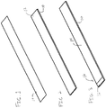
- FIG. 1 shows a single unit as cut from such a larger sheet to illustratively show the fabrication of the single unit.
- the first biocompatible dielectric layer 10 will form the outer layer of a sensor equipped needle or other device.
- the dielectric layer 10 may be about 25 - 50 microns thick although other thicknesses may be employed.
- a conductive layer 12 is formed on layer 10.
- the conductive layer 12 will form an outer shield for the sensor equipped needle or other device.
- the conductive layer 12 may include a foil adhered to layer 10, include conductive ink, include an evaporated metal, etc.
- a middle insulating layer 14 is deposited or formed over the conductive layer 12. At a hub end portion 16 of the strip, the middle insulating layer 14 does not extend to the end, so a small strip of the outer shield or conductive layer 12 remains exposed. This exposed end will eventually form a hub end ring electrode for the outer shield 12 that a needle connector (not shown) will connect to.
- the insulating layer 14 may be about 25 - 50 microns thick although other thicknesses may be employed.
- a conductive signal trace 18 is formed on the middle insulating layer 14.
- the trace 18 may be deposited and selectively etched to provide T-shaped end patterns 20, 22.
- the T shaped end pattern 22 will form an electrode 26 that will cover the sensor to be formed.
- the T shaped section 20 will form a ring or hub electrode 28 that a needle connector uses to connect to the signal trace 18.
- the conductive signal trace layer may include a thickness from about less than on micron to a few microns, although other thicknesses may be employed.
- the electrodes 26, 28 and the trace 18 may be printed using a conductive ink. Other processes may be employed as well such as, e.g., masked vapor deposition or vapor deposition and etching.
- the signal trace 18 is then covered with another insulating layer 30.
- This insulating layer 30 will be on the side of the film that will come in contact with the needle or other device on which the sensor will be placed. At the tip end portion 24, the insulating layer 30 will leave the sensor electrode exposed, and at the hub end portion 16, the insulating layer 30 leaves the hub electrode 28 exposed.
- the insulating 18 may be about 25 - 50 microns thick although other thicknesses may be employed.
- a structure 40 shown in FIG. 5 may include very thin but strong laminates for its layers, so that the structure 40 will not stretch and damage the conductive components formed therein.
- One or more of the insulating layers 10 may include, e.g., polyurethane, although other plastics or insulating materials may be employed.
- the conductive layer 12 may include a foil and may be aluminum, silver, gold or other biocompatible conductors.
- the structure 40 includes a width that may be less than a circumference of the needle or device on which it will be placed. In particularly useful embodiments, the width could be between, for example, about 20% of the circumference to about 90% the circumference.
- the structure 40 can be attachable to a needle 42 by bending the structure 40 into a tubular shape. Layer 30 will be in contact with the needle 42 (or other device).
- the structure 40 includes a width that wraps around the needle 42 and is slightly smaller than a diameter of the needle 42. When installed on the needle 42, edges of the structure 40 form a gap 44 running along the length (or a substantial portion of the length) of the needle 42.
- the hub end portion 16 is shown in FIG. 6 .
- an elastic strip 46 may, for example, be accomplished by gluing the elastic strip to the edges of the structure 40, or applying a glue that dries into an elastic material in the gap 44 when the structure 40 is wrapped around a template needle and then transferred to needle 42.
- the dielectric layer 10 in FIG. 1 may be formed from a material where the width covers a tube circumference (needle circumference), and makes the other insulator layers closer to the needle 42 (in the stack of layers) narrower (less width) so they make a more rigid structure 40.
- a small portion of the conductive layer 12 and T-shape 20 may be folded back (cuffed) onto itself (e.g., folding the exposed strip onto itself at the very end before making it into a tube shape). This brings the contact points for the outer shield 12 and the T shape 20 signal trace from an inside surface of the formed tube to an outside of the tube, so that a clamp style connector can attach to these contact points.
- a single ring sensor 50 may be formed at the tip end portion 24 of the needle 42 in accordance with one embodiment.
- the needle 42 preferably includes a metal, such as a stainless steel although other surgically compatible materials may be employed.
- the tip end portion 24 (distal end portion) of the needle 42 may be coated with a piezoelectric copolymer 32. This may be achieved by employing a dip coating process.
- the metal needle 42 now serves as a bottom electrode for the copolymer sensor 50.
- the top electrode of the sensor 50 will be the electrode 26.
- the copolymer may include a PVDF or P(VDF-TrFE) ring, although other suitable materials may be employed.
- dielectric/insulating layers e.g., layers 10, 14, 30 ( FIG.5 )
- a material with a relatively low dielectric constant For example, polytetrafluoroethylene (PTFE) with a dielectric constant of about 2.1 may be selected.
- PTFE polytetrafluoroethylene
- Other materials such as biocompatible polypropylene (dielectric constant 2.2) may be employed.
- Many plastics/polymers have a dielectric constant close to 3.0 and may also be employed.
- Polyurethane has a slightly higher 3.5 value and is attractive for use in the present applications because there are medical grade versions (used to coat implantable pacemakers). Further, polyurethane provides good adhesion to many materials with high smoothness and durability, and can be deposited in thin layers using appropriate solvents. Other materials may also be used.
- the present principles can be extended to multiple sensors on a same needle. This permits a determination of an orientation of the needle and also a determination of the location of the needle tip without the need to place the sensor very close to the tip. Calculating the tip location based on signals from multiple sensors should also increase the measurement accuracy as well as provide an indication of confidence in the measurement. The cost is a slightly more complicated manufacturing process and a slight loss of signal because of the extra capacitive load of multiple sensors.
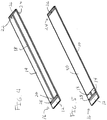
- another embodiment includes a slanted strip 102 that can be attached to a needle or device using a spiral outer wrap.
- the slanted strip 102 in this embodiment includes embedded piezoelectric sensors and interconnects (traces).
- an insulator 104 in the form of the slanted strip 102 includes thongs or cross-strips 106.
- the thongs 106 will include the sensors and are angled relative to the strip 102 so that when the strip 102 is lightly spirally wound about a needle (not shown), the thongs 106 will form rings around the needle.
- the insulator 104 may include one or more of the dielectric materials described above, e.g., polyurethane, Mylar, etc.
- the strip 102 includes an acutely slanted end portion 103 to enable a starting position for spirally wrapping the strip on the medical device.
- a bottom electrode or electrodes 108 are formed along with a trace or traces 110 connecting the bottom electrodes 108.
- the conductive material for the bottom electrodes 108 and traces 110 may include conductive ink, evaporated metals, conductive polymers, etc.
- a piezoelectric material 112 (e.g., PVDF or copolymer material) is applied to the thongs 106 only.
- the piezoelectric material 112 may be deposited using masks or the like or may be painted on.
- a top electrode or electrodes 114 are applied on top of the piezoelectric material 112 and formed along with a trace 116 connecting them and forming sensors 120.
- a multi-sensor needle is provided with a shared trace connecting the sensors.
- the slanted strip 102 can be wound around the needle in a slightly spiraling manner.
- a first layer that touches a needle 122 can be adhesive in nature.
- a securing feature 123 such as a film may be made in the form of a very narrow strip.
- This feature 123 includes one or more insulators 125 and a conductive layer 127.
- the conductive layer 127 may be sandwiched between insulators.
- the strip 102 (and/or the feature 123) is wound around the needle 122 in a tightly packed dense spiral that fully covers the needle 122.
- the feature 123 includes an outer biocompatible insulation layer 125, and an outer shield (conductive layer 127).
- the inner insulator (not shown) of this feature 123 can be adhesive in nature.
- Alternate embodiments may include, for example, a structure where the sensors are directly in contact with a needle where the needle functions as one electrode (as in FIG. 7 ).
- a partially elastic tube with interconnects with piezoelectric sensors deposited on the tube may be employed.
- the structure 40 of FIG. 5 could be attached to a needle in a spiral as in FIG. 12 .
- a very narrow adhesive strip could be spiraled around the structure 40 in FIG. 6 , this strip could form the outer biocompatible insulator (so the layer 30 in FIG. 5 would no longer be needed).
- a thin wire may be used to spiral around the structure 40 in FIG. 6 .
- the wire may have an adhesive coating or a non-adhesive wire may be employed followed by dipcoating in a biocompatible glue/encapsulant.
- a tube such as a heatshrink tube or similar material, such as a material that shrinks when exposed to a chemical or UV light may be employed to encapsulate a strip (spiraled or wrapped) in accordance with the present principles.
- the sensors may include PVDF or copolymer, or the sensors may include, for example, PZT or another piezoelectric material, or an altogether different sensor, such as, a capacitive micromachined ultrasound transducer (CMUT).
- CMUT capacitive micromachined ultrasound transducer
- an adhesive layer could be applied to the needle, and the strips or structures described may be pressed around or spiraled around the needle to adhere them.
- piezoelectrical polymers such as PVDF and P(VDF-TrFE) are candidate materials for sensor production.
- the ability of an applied voltage to produce motion in a PVDF sample is used to produce ultrasonic waves which can be detected using a PVDF based hydrophone.
- PVDF piezoelectrical polymers
- a PVDF sensor can be modeled as a voltage source in series with a capacitance and for thicker sensors with small surface area. This results in a small capacitance.
- PVDF has advantages for medical ultrasonic work carried out in the frequency range 25-100 MHz.
- PVDF is also limited in ability to transmit higher intensities of ultrasound compared to PZT.
- PVDF has favorable behavior even at the lower frequencies, for example, for PVDF hydrophones for detecting ultrasonic waves.
- PVDF has a much higher bandwidth and will thus not distort the transient behavior of the wave as much.
- the low output capacitance problem can in this case be handled by integrating a high input impedance field effect transistor (FET) based preamplifier in very close proximity to the sensor.
- FET field effect transistor
- the acoustic impedance of piezo film is about 4 MRayls, a much better match.
- ceramics are fragile, and cannot be shaped to desired geometries.
- PVDF is a conformable and flexible low cost material with acoustic impedance close to tissue that unlike PZT will not need matching layers.
- PVDF piezoelectric films are produced in a clean room environment, and start with a melt extrusion of PVDF resin pellets into sheet form. Next, there is a stretching step that reduces the sheet thickness by about a factor of 5. This stretching, well below the melting point of the polymer, causes chain packing of the molecules into parallel crystal planes, called the "beta phase". To obtain high levels of piezoelectric activity, the beta phase polymer is then exposed to very high electric fields to align the crystallites relative to a poling field. In the stretching step, the film can be stretched along only one dimension (uni-axial film) or in both dimensions (bi-axial film). Bi-axial films will have their piezoelectric sensitivity primarily only in the thickness direction, while the uni-axial film will be sensitive to strain in both the thickness direction and the non-stretched planar direction.
- Copolymers of PVDF have been developed that allow for use at higher temperatures (e.g., as high as 135 degrees Celsius for some copolymers, versus 100 degrees Celsius for conventional PVDF). Although these temperatures are not encountered in clinical use, a higher temperature tolerance can be an advantage in simplifying the manufacturing and sterilization process.
- Copolymers of PVDF are polarizable without stretching and very thin films down to 200 Angstroms can be produced using spincast coating techniques, such thin layers are not feasible with standard PVDF.
- the copolymer has a slightly higher thickness mode piezoelectric constant, leading to about 10% higher sensitivity compared to PVDF.
- the present principles have been described in terms of a needle, and more particularly to a biopsy needle. However, the present principles may be applied to nay instrument where a piezoelectric sensor (receiver), transmitter or transducer is needed. Such devices may include catheters, guidewires, endoscopes, implantable devices, etc.
- the present principles can provide a relatively low cost device with a built-in for sensor conformally applied to an exterior surface. To keep the product cost down, the materials used need to be low cost, and the manufacturing process should be highly automated with large volume to avoid labor and equipment cost.
- the devices in accordance with the present principles provide a low form factor that is conformally formed and placed on a medical device or instrument. In particularly useful embodiments, the present principles are employed for ultrasound guided needle interventions, e.g., RF ablation, liver biopsy, nerve blocks, vascular access, abscess drainage, etc.
- a flexible planar strip having a plurality of layers including dielectric materials and sensor components is provided in accordance with the present embodiments.
- the sensor components may be completely on the strip, or partially on the strip and partially on the medical device
- the flexible planar strip is wrapped about a medical device to at least partially encapsulate the medical device.
- the flexible planar strip may be wrapped around a medical device, e.g., a needle, having a piezoelectric polymer coating such that a sensor electrode on the strip contacts the piezoelectric polymer to form the at least one sensor.
- the flexible planar strip is wrapped about at least a portion of a circumference of the device wherein the securing feature is configured to secure edges of the strip over the medical device.
- the flexible planar strip is spirally wrapped about the medical device.
- the flexible planar strip may include at least one thong that forms an angle with the strip such that when the strip is spiraled about the medical device, the thong forms a ring sensor around the medical device.
- the strip is secured to the medical device using a securing feature over the strip such that at least one sensor device is provided on the medical device by application of the strip on the medical device.
- the securing feature is configured to wrap around the strip and includes a conductor to form a shield and at least one dielectric layer (e.g., for the spirally wrapped embodiment).
- the conductor may include a wire with or without adhesive or dielectric thereon.
- the strip may include a conductive shield and a hub electrode on a proximal end portion, the conductive shield and the hub electrode may be cuffed to permit external electrical connections to the conductive shield and the hub electrode.
- an external connector is applied to electrically connect the sensor to electronics.
- the sensor or sensors can now be employed to make measurements.
- the sensors measure ultrasonic energy for guided needle applications. Other applications and devices are also contemplated.
Description
- This disclosure relates to medical instruments and more particularly to a system and method for applying ultrasound receivers on a device using planar thin film methods.
- In ultrasound imaging, the visibility of the needle is often very poor due to the specular nature of the needle surface that reflects beams away from the imaging probe. To alleviate this problem some needle manufacturers have produced needles with special echogenic coatings, but the visualization improvement is limited. Ultrasound imaging system manufacturers have developed algorithms that use multiple imaging beams from varied angles, but improvement is limited and such a strategy is primarily suited only for linear arrays. Both strategies do not help when the needle is inserted perpendicular to the imaging plane, or the needle path has a small offset relative to the imaging plane.
- One solution that has been proposed to visualize the tip of interventional tools such as needles, but also catheters, is to add ultrasound receivers near the tip of the tool. While the imaging beam sweeps the field of view, the signals from the sensors indicate how close the beams are getting to the sensor. This information is used to calculate sensor position relative to the ultrasound image with positional accuracy exceeding 0.5 mm, even under conditions where the needle is not visible in the ultrasound image. The sensor needs to not interfere with the functionality of the device (e.g., an automatic biopsy device), that is, not block the lumen, not interfere with the mechanics, etc.
-
US 5 830 144 A discloses a tracking data sheath arrangable on a variety of different surgical instruments (e.g., catheters and probes) to provide the surgical instruments with 3-D tracking capability. The tracking data sheath being generally elastomeric or rigid for convenient installation and removal, and having transducers and conductors embedded therein.WO 2009/006335 A1 discloses a catheter with a helically wrapped planar flexible strip having conductors for making contact with a distal ultrasound transducer. - The invention is defined in claim 1, 8 and 11. Preferred embodiments of the invention are defined in the dependent claims.
- In accordance with the present principles, a sensor device includes a flexible planar strip including a plurality of layers. The strip is configured to at least partially encapsulate a medical device. The strip includes a first dielectric layer, a conductive shield layer disposed on the first dielectric layer, a second dielectric layer formed on the conductive shield layer; and a patterned conductive layer including a sensor electrode, a hub electrode and a trace connecting the sensor electrode and the hub electrode.
- Another sensor device includes a flexible planar strip including a plurality of layers, the strip being configured to spirally wrap around a medical device to at least partially encapsulate the medical device. The strip includes a first dielectric layer of the strip having at least one angled end portion and including at least one thong extending transversely from a longitudinal dimension of the strip. A bottom electrode and a bottom electrode trace, which connects to the bottom electrode, are formed on the first dielectric layer. A piezoelectric layer is formed on the bottom electrode. A top electrode and a top electrode trace, which connects to the top electrode, are formed on the piezoelectric layer.
- A method for applying a sensor to a medical device includes providing a flexible planar strip having a plurality of layers including dielectric materials and sensor components; wrapping the flexible planar strip about a medical device to at least partially encapsulate the medical device; and securing the strip to the medical device using a securing feature over the strip such that at least one sensor device is provided on the medical device by application of the strip on the medical device.
- These and other objects, features and advantages of the present disclosure will become apparent from the following detailed description of illustrative embodiments thereof, which is to be read in connection with the accompanying drawings.
- This disclosure will present in detail the following description of preferred embodiments with reference to the following figures wherein:
-
FIG. 1 is a perspective view showing a flexible planar dielectric layer for forming a low profile conformal sensor device in accordance with the present principles; -
FIG. 2 is a perspective view showing the device ofFIG. 1 having a conductive shield layer formed thereon in accordance with the present principles; -
FIG. 3 is a perspective view showing the device ofFIG. 2 having a middle insulating layer formed thereon in accordance with the present principles; -
FIG. 4 is a perspective view showing the device ofFIG. 3 having a top electrode, hub contact and trace formed on the middle insulating layer in accordance with the present principles; -
FIG. 5 is a perspective view showing the device ofFIG. 4 having another dielectric layer (insulator) formed on the trace in accordance with the present principles; -
FIG. 6 is a perspective view showing the device ofFIG. 5 being wrapped about a hub end of a needle in accordance with the present principles; -
FIG. 7 is a side view showing the device ofFIG. 5 being applied about a tip end of a needle with a piezoelectric material employed to form a sensor in accordance with the present principles; -
FIG. 8 is a top view of a slanted strip with thongs for forming a spirally wrapped sensor device in accordance with the present principles; -
FIG. 9 is a top view showing the device ofFIG. 8 with bottom electrodes (and traces) being applied in accordance with the present principles; -
FIG. 10 is a top view showing the device ofFIG. 9 with a piezoelectric material being applied to the bottom electrodes in accordance with the present principles; -
FIG. 11 is a top view showing the device ofFIG. 10 with top electrodes (and traces) being applied in accordance with the present principles; -
FIG. 12 is a side view showing a spirally wrapped sensor device and a securing feature in accordance with the present principles; and -
FIG. 13 is a flow diagram showing a method for applying a sensor device in accordance with illustrative embodiments. - In accordance with the present principles, systems, devices and methods are provided for applying a sensor or sensors to a needle (or other device) to implement ultrasound guidance or tracking of the needle or device. The present principles provide a needle, device or system that includes one or more low profile sensors at very low per device cost and permits scaling for mass production to maintain low cost. In one embodiment, an interconnect for the sensor may be mass manufactured on a large planar thin film sheet (with a repeating pattern) and subsequently cut into thin strips. Methods are described for attaching these strips to the device. In one method, a highly bendable/flexible material is employed for the sheet, and the sheet is wrapped about a circumference of the device. In another method, a strip is wrapped around the needle in a spiraling manner. In these and other methods, a sensor device is formed on a thin planar film, which is to be mounted on the device.
- The ultrasound sensors may be formed on a thin film planar sheet by building dielectric layers and patterning conductors such that the entire sensor (or a portion of the sensor) is formed prior to its mounting on the device. The needle or other device may be fabricated using a piezoelectric polymer, e.g., polyvinylidene fluoride (PVDF) or polyvinylidene fluoride trifluoroethylene (P(VDF-TrFE)). P(VDF-TrFE). These materials can be dissolved in acetone and applied to the planar sheet or to the medical device through an evaporative process. The sensors are high impedance and can be modeled as a voltage source in series with a small capacitor (e.g., 2.2pF). Such a sensor is very sensitive to capacitive loading of the electrical interconnect, and special capacitance cancelling electronics (similar to, e.g., a driven shield technique) can be employed to avoid large signal loss. A wire or trace carrying the signal preferably is shielded (e.g., includes an electric shield around the conductor). This may be accomplished using a stripline configuration.
- It should be understood that the present invention will be described in terms of medical instruments; however, the teachings of the present invention are much broader and are applicable to any instrument that can accept a low profile sensor. In some embodiments, the present principles are employed in tracking or analyzing complex biological or mechanical systems. In particular, the present principles are applicable to internal tracking procedures of biological systems and are applicable for procedures in all areas of the body such as the lungs, gastro-intestinal tract, excretory organs, blood vessels, etc. The elements depicted in the FIGS. may be implemented in various combinations of hardware and software and provide functions which may be combined in a single element or multiple elements.
- Moreover, all statements herein reciting principles, aspects, and embodiments of the invention, as well as specific examples thereof, are intended to encompass both structural and functional equivalents thereof. Additionally, it is intended that such equivalents include both currently known equivalents as well as equivalents developed in the future (i.e., any elements developed that perform the same function, regardless of structure). Thus, for example, it will be appreciated by those skilled in the art that the block diagrams presented herein represent conceptual views of illustrative system components and/or circuitry embodying the principles of the invention. Similarly, it will be appreciated that any flow charts, flow diagrams and the like represent various processes which may be substantially represented in computer readable storage media and so executed by a computer or processor, whether or not such computer or processor is explicitly shown.
- It will also be understood that when an element such as a layer, region or material is referred to as being "on" or "over" another element, it can be directly on the other element or intervening elements may also be present. In contrast, when an element is referred to as being "directly on" or "directly over" another element, there are no intervening elements present. It will also be understood that when an element is referred to as being "connected" or "coupled" to another element, it can be directly connected or coupled to the other element or intervening elements may be present. In contrast, when an element is referred to as being "directly connected" or "directly coupled" to another element, there are no intervening elements present.
- Reference in the specification to "one embodiment" or "an embodiment" of the present principles, as well as other variations thereof, means that a particular feature, structure, characteristic, and so forth described in connection with the embodiment is included in at least one embodiment of the present principles. Thus, the appearances of the phrase "in one embodiment" or "in an embodiment", as well any other variations, appearing in various places throughout the specification are not necessarily all referring to the same embodiment.
- It is to be appreciated that the use of any of the following "/", "and/or", and "at least one of', for example, in the cases of "A/B", "A and/or B" and "at least one of A and B", is intended to encompass the selection of the first listed option (A) only, or the selection of the second listed option (B) only, or the selection of both options (A and B). As a further example, in the cases of "A, B, and/or C" and "at least one of A, B, and C", such phrasing is intended to encompass the selection of the first listed option (A) only, or the selection of the second listed option (B) only, or the selection of the third listed option (C) only, or the selection of the first and the second listed options (A and B) only, or the selection of the first and third listed options (A and C) only, or the selection of the second and third listed options (B and C) only, or the selection of all three options (A and B and C). This may be extended, as readily apparent by one of ordinary skill in this and related arts, for as many items listed.
- Referring now to the drawings in which like numerals represent the same or similar elements and initially to
FIG. 1 , a perspective view of adielectric layer 10 is shown in accordance with one embodiment. Thedielectric layer 10 may be formed as a sheet and represents and outer biocompatible insulation layer. The biocompatible insulation material forlayer 10 may include Mylar, pressure sensitive adhesive films, polyester films, polyimide films, parylene, polyurethane, etc. The sheet on which thedielectric layer 10 is formed may be first manufactured on a large planar thin film sheet. One sheet may include a plurality of structures. Then, individual units can be cut from the sheet using, for example, laser cutting, stamping, etc. Thedielectric layer 10 may be the first layer in the sheet as the layers and components will be constructed from an outermost layer to an innermost layer; however, the fabrication order may be reversed or otherwise changed, as needed.FIG. 1 shows a single unit as cut from such a larger sheet to illustratively show the fabrication of the single unit. The firstbiocompatible dielectric layer 10 will form the outer layer of a sensor equipped needle or other device. Thedielectric layer 10 may be about 25 - 50 microns thick although other thicknesses may be employed. - Referring to
FIG. 2 , aconductive layer 12 is formed onlayer 10. Theconductive layer 12 will form an outer shield for the sensor equipped needle or other device. Theconductive layer 12 may include a foil adhered to layer 10, include conductive ink, include an evaporated metal, etc. - Referring to
FIG. 3 , a middle insulatinglayer 14 is deposited or formed over theconductive layer 12. At ahub end portion 16 of the strip, the middle insulatinglayer 14 does not extend to the end, so a small strip of the outer shield orconductive layer 12 remains exposed. This exposed end will eventually form a hub end ring electrode for theouter shield 12 that a needle connector (not shown) will connect to. The insulatinglayer 14 may be about 25 - 50 microns thick although other thicknesses may be employed. - Referring to
FIG. 4 , aconductive signal trace 18 is formed on the middle insulatinglayer 14. Thetrace 18 may be deposited and selectively etched to provide T-shapedend patterns end pattern 22 will form anelectrode 26 that will cover the sensor to be formed. At the hub end portion 16 (proximal end portion), the T shapedsection 20 will form a ring orhub electrode 28 that a needle connector uses to connect to thesignal trace 18. The conductive signal trace layer may include a thickness from about less than on micron to a few microns, although other thicknesses may be employed. In one embodiment, theelectrodes trace 18 may be printed using a conductive ink. Other processes may be employed as well such as, e.g., masked vapor deposition or vapor deposition and etching. - Referring to
FIG. 5 , thesignal trace 18 is then covered with another insulatinglayer 30. This insulatinglayer 30 will be on the side of the film that will come in contact with the needle or other device on which the sensor will be placed. At thetip end portion 24, the insulatinglayer 30 will leave the sensor electrode exposed, and at thehub end portion 16, the insulatinglayer 30 leaves thehub electrode 28 exposed. The insulating 18 may be about 25 - 50 microns thick although other thicknesses may be employed. - A
structure 40 shown inFIG. 5 may include very thin but strong laminates for its layers, so that thestructure 40 will not stretch and damage the conductive components formed therein. One or more of the insulatinglayers 10 may include, e.g., polyurethane, although other plastics or insulating materials may be employed. Theconductive layer 12 may include a foil and may be aluminum, silver, gold or other biocompatible conductors. Thestructure 40 includes a width that may be less than a circumference of the needle or device on which it will be placed. In particularly useful embodiments, the width could be between, for example, about 20% of the circumference to about 90% the circumference. - Referring to
FIG. 6 , thestructure 40 can be attachable to aneedle 42 by bending thestructure 40 into a tubular shape.Layer 30 will be in contact with the needle 42 (or other device). Thestructure 40 includes a width that wraps around theneedle 42 and is slightly smaller than a diameter of theneedle 42. When installed on theneedle 42, edges of thestructure 40 form agap 44 running along the length (or a substantial portion of the length) of theneedle 42. Thehub end portion 16 is shown inFIG. 6 . - Between the edges of the
gap 44, a different material may be applied that is highly elastic to form a stretchable tube that can slide over theneedle 42. Application of anelastic strip 46 may, for example, be accomplished by gluing the elastic strip to the edges of thestructure 40, or applying a glue that dries into an elastic material in thegap 44 when thestructure 40 is wrapped around a template needle and then transferred toneedle 42. - In one embodiment, the
dielectric layer 10 inFIG. 1 may be formed from a material where the width covers a tube circumference (needle circumference), and makes the other insulator layers closer to the needle 42 (in the stack of layers) narrower (less width) so they make a morerigid structure 40. - At the
hub end portion 16, a small portion of theconductive layer 12 and T-shape 20 may be folded back (cuffed) onto itself (e.g., folding the exposed strip onto itself at the very end before making it into a tube shape). This brings the contact points for theouter shield 12 and theT shape 20 signal trace from an inside surface of the formed tube to an outside of the tube, so that a clamp style connector can attach to these contact points. - Referring to
FIG. 7 , asingle ring sensor 50 may be formed at thetip end portion 24 of theneedle 42 in accordance with one embodiment. Theneedle 42 preferably includes a metal, such as a stainless steel although other surgically compatible materials may be employed. The tip end portion 24 (distal end portion) of theneedle 42 may be coated with apiezoelectric copolymer 32. This may be achieved by employing a dip coating process. Themetal needle 42 now serves as a bottom electrode for thecopolymer sensor 50. The top electrode of thesensor 50 will be theelectrode 26. In one embodiment, the copolymer may include a PVDF or P(VDF-TrFE) ring, although other suitable materials may be employed. - For the dielectric/insulating layers, e.g., layers 10, 14, 30 (
FIG.5 ), it is advantageous to select a material with a relatively low dielectric constant. For example, polytetrafluoroethylene (PTFE) with a dielectric constant of about 2.1 may be selected. However, the adhesion of PTFE to other materials may be an issue. Other materials, such as biocompatible polypropylene (dielectric constant 2.2) may be employed. Many plastics/polymers have a dielectric constant close to 3.0 and may also be employed. Polyurethane has a slightly higher 3.5 value and is attractive for use in the present applications because there are medical grade versions (used to coat implantable pacemakers). Further, polyurethane provides good adhesion to many materials with high smoothness and durability, and can be deposited in thin layers using appropriate solvents. Other materials may also be used. - The present principles can be extended to multiple sensors on a same needle. This permits a determination of an orientation of the needle and also a determination of the location of the needle tip without the need to place the sensor very close to the tip. Calculating the tip location based on signals from multiple sensors should also increase the measurement accuracy as well as provide an indication of confidence in the measurement. The cost is a slightly more complicated manufacturing process and a slight loss of signal because of the extra capacitive load of multiple sensors.
- Referring to
FIGS. 8-11 , another embodiment includes a slanted strip 102 that can be attached to a needle or device using a spiral outer wrap. The slanted strip 102 in this embodiment includes embedded piezoelectric sensors and interconnects (traces). - Referring to
FIG. 8 , aninsulator 104 in the form of the slanted strip 102 includes thongs orcross-strips 106. Thethongs 106 will include the sensors and are angled relative to the strip 102 so that when the strip 102 is lightly spirally wound about a needle (not shown), thethongs 106 will form rings around the needle. Theinsulator 104 may include one or more of the dielectric materials described above, e.g., polyurethane, Mylar, etc. The strip 102 includes an acutely slanted end portion 103 to enable a starting position for spirally wrapping the strip on the medical device. - Referring to
FIG. 9 , a bottom electrode or electrodes 108 are formed along with a trace or traces 110 connecting the bottom electrodes 108. The conductive material for the bottom electrodes 108 and traces 110 may include conductive ink, evaporated metals, conductive polymers, etc. - Referring to
FIG. 10 , a piezoelectric material 112 (e.g., PVDF or copolymer material) is applied to thethongs 106 only. Thepiezoelectric material 112 may be deposited using masks or the like or may be painted on. - Referring to
FIG. 11 , a top electrode orelectrodes 114 are applied on top of thepiezoelectric material 112 and formed along with a trace 116 connecting them and formingsensors 120. In this embodiment, a multi-sensor needle is provided with a shared trace connecting the sensors. - Referring to
FIG. 12 , the slanted strip 102 can be wound around the needle in a slightly spiraling manner. A first layer that touches aneedle 122 can be adhesive in nature. To hold this structure rigidly on theneedle 122, a securingfeature 123 such as a film may be made in the form of a very narrow strip. Thisfeature 123 includes one ormore insulators 125 and aconductive layer 127. Theconductive layer 127 may be sandwiched between insulators. The strip 102 (and/or the feature 123) is wound around theneedle 122 in a tightly packed dense spiral that fully covers theneedle 122. Thefeature 123 includes an outerbiocompatible insulation layer 125, and an outer shield (conductive layer 127). The inner insulator (not shown) of thisfeature 123 can be adhesive in nature. - Alternate embodiments may include, for example, a structure where the sensors are directly in contact with a needle where the needle functions as one electrode (as in
FIG. 7 ). In other embodiments, a partially elastic tube with interconnects with piezoelectric sensors deposited on the tube may be employed. - In one embodiment, the
structure 40 ofFIG. 5 could be attached to a needle in a spiral as inFIG. 12 . A very narrow adhesive strip could be spiraled around thestructure 40 inFIG. 6 , this strip could form the outer biocompatible insulator (so thelayer 30 inFIG. 5 would no longer be needed). Instead of the narrow adhesive strip, a thin wire may be used to spiral around thestructure 40 inFIG. 6 . The wire may have an adhesive coating or a non-adhesive wire may be employed followed by dipcoating in a biocompatible glue/encapsulant. - In one embodiment, a tube, such as a heatshrink tube or similar material, such as a material that shrinks when exposed to a chemical or UV light may be employed to encapsulate a strip (spiraled or wrapped) in accordance with the present principles.
- In other embodiments, the sensors may include PVDF or copolymer, or the sensors may include, for example, PZT or another piezoelectric material, or an altogether different sensor, such as, a capacitive micromachined ultrasound transducer (CMUT).
- In one embodiment, an adhesive layer could be applied to the needle, and the strips or structures described may be pressed around or spiraled around the needle to adhere them.
- To keep the product cost down, the materials used should be low cost, and the manufacturing process should be highly automated with large volume to avoid labor and equipment cost. Given these goals, piezoelectrical polymers such as PVDF and P(VDF-TrFE) are candidate materials for sensor production. The ability of an applied voltage to produce motion in a PVDF sample is used to produce ultrasonic waves which can be detected using a PVDF based hydrophone. There are a wide variety of considerations in deciding whether to use a ceramic based piezoelectric or PVDF in a given medical application. At lower frequencies thicker PVDF membranes should be employed for resonance considerations. A PVDF sensor can be modeled as a voltage source in series with a capacitance and for thicker sensors with small surface area. This results in a small capacitance. Hence, in general, it appears that PVDF has advantages for medical ultrasonic work carried out in the frequency range 25-100 MHz. PVDF is also limited in ability to transmit higher intensities of ultrasound compared to PZT.
- PVDF has favorable behavior even at the lower frequencies, for example, for PVDF hydrophones for detecting ultrasonic waves. Compared to PZT, which may also be employed in some embodiments, PVDF has a much higher bandwidth and will thus not distort the transient behavior of the wave as much. The low output capacitance problem can in this case be handled by integrating a high input impedance field effect transistor (FET) based preamplifier in very close proximity to the sensor. The d33 constant, strain in thickness direction developed for an applied voltage, is about an order of magnitude higher for piezo-ceramics than for piezo-polymers. One disadvantage of piezo-ceramic is its high acoustic impedance, about 30 MRayls (1 MRayl = 106 kg/m2s) in contrast to about 1.5 MRayls for body tissue. This impedance mismatch can be compensated by quarter wavelength matching layers, but these can degrade the ultrasonic pulse due to adhesive layers and construction methods. The acoustic impedance of piezo film is about 4 MRayls, a much better match. Additionally, ceramics are fragile, and cannot be shaped to desired geometries. PVDF is a conformable and flexible low cost material with acoustic impedance close to tissue that unlike PZT will not need matching layers.
- PVDF piezoelectric films are produced in a clean room environment, and start with a melt extrusion of PVDF resin pellets into sheet form. Next, there is a stretching step that reduces the sheet thickness by about a factor of 5. This stretching, well below the melting point of the polymer, causes chain packing of the molecules into parallel crystal planes, called the "beta phase". To obtain high levels of piezoelectric activity, the beta phase polymer is then exposed to very high electric fields to align the crystallites relative to a poling field. In the stretching step, the film can be stretched along only one dimension (uni-axial film) or in both dimensions (bi-axial film). Bi-axial films will have their piezoelectric sensitivity primarily only in the thickness direction, while the uni-axial film will be sensitive to strain in both the thickness direction and the non-stretched planar direction.
- New copolymers of PVDF have been developed that allow for use at higher temperatures (e.g., as high as 135 degrees Celsius for some copolymers, versus 100 degrees Celsius for conventional PVDF). Although these temperatures are not encountered in clinical use, a higher temperature tolerance can be an advantage in simplifying the manufacturing and sterilization process. Copolymers of PVDF are polarizable without stretching and very thin films down to 200 Angstroms can be produced using spincast coating techniques, such thin layers are not feasible with standard PVDF. In addition the copolymer has a slightly higher thickness mode piezoelectric constant, leading to about 10% higher sensitivity compared to PVDF.
- The present principles have been described in terms of a needle, and more particularly to a biopsy needle. However, the present principles may be applied to nay instrument where a piezoelectric sensor (receiver), transmitter or transducer is needed. Such devices may include catheters, guidewires, endoscopes, implantable devices, etc. The present principles can provide a relatively low cost device with a built-in for sensor conformally applied to an exterior surface. To keep the product cost down, the materials used need to be low cost, and the manufacturing process should be highly automated with large volume to avoid labor and equipment cost. The devices in accordance with the present principles provide a low form factor that is conformally formed and placed on a medical device or instrument. In particularly useful embodiments, the present principles are employed for ultrasound guided needle interventions, e.g., RF ablation, liver biopsy, nerve blocks, vascular access, abscess drainage, etc.
- Referring to
FIG. 13 , methods for applying a sensor to a medical device are illustrative shown. Inblock 202, a flexible planar strip having a plurality of layers including dielectric materials and sensor components is provided in accordance with the present embodiments. The sensor components may be completely on the strip, or partially on the strip and partially on the medical device - In
block 204, the flexible planar strip is wrapped about a medical device to at least partially encapsulate the medical device. Inblock 206, the flexible planar strip may be wrapped around a medical device, e.g., a needle, having a piezoelectric polymer coating such that a sensor electrode on the strip contacts the piezoelectric polymer to form the at least one sensor. Inblock 208, the flexible planar strip is wrapped about at least a portion of a circumference of the device wherein the securing feature is configured to secure edges of the strip over the medical device. Inblock 210, the flexible planar strip is spirally wrapped about the medical device. Inblock 211, the flexible planar strip may include at least one thong that forms an angle with the strip such that when the strip is spiraled about the medical device, the thong forms a ring sensor around the medical device. - In
block 212, the strip is secured to the medical device using a securing feature over the strip such that at least one sensor device is provided on the medical device by application of the strip on the medical device. In one embodiment, the securing feature is configured to wrap around the strip and includes a conductor to form a shield and at least one dielectric layer (e.g., for the spirally wrapped embodiment). The conductor may include a wire with or without adhesive or dielectric thereon. - In
block 214, the strip may include a conductive shield and a hub electrode on a proximal end portion, the conductive shield and the hub electrode may be cuffed to permit external electrical connections to the conductive shield and the hub electrode. - In
block 216, an external connector is applied to electrically connect the sensor to electronics. The sensor or sensors can now be employed to make measurements. In particularly useful embodiments, the sensors measure ultrasonic energy for guided needle applications. Other applications and devices are also contemplated. - In interpreting the appended claims, it should be understood that:
- a) the word "comprising" does not exclude the presence of other elements or acts than those listed in a given claim;
- b) the word "a" or "an" preceding an element does not exclude the presence of a plurality of such elements;
- c) any reference signs in the claims do not limit their scope;
- d) several "means" may be represented by the same item or hardware or software implemented structure or function; and
- e) no specific sequence of acts is intended to be required unless specifically indicated.
- Having described preferred embodiments for needle with thin film piezoelectric sensors (which are intended to be illustrative and not limiting), it is noted that modifications and variations can be made by persons skilled in the art in light of the above teachings. It is therefore to be understood that changes may be made in the particular embodiments of the disclosure disclosed which are within the scope of the embodiments disclosed herein as outlined by the appended claims. Having thus described the details and particularity required by the patent laws, what is claimed and desired protected by Letters Patent is set forth in the appended claims.
Claims (14)
- A sensor device for wrapping around a needle (42), the sensor device comprising:
a flexible planar strip (40) including a plurality of layers, the flexible planar strip (40) having a distal end portion (24) and a proximal end portion (16) and being configured to at least partially encapsulate the needle (42), the flexible planar strip (40) including:a first dielectric layer (10);a conductive shield layer (12) disposed on the first dielectric layer (10);a second dielectric layer (14) formed on the conductive shield layer (12);a patterned conductive layer disposed on the second dielectric layer (14), the patterned conductive layer including a sensor electrode (26) disposed at the distal end portion (24), a hub electrode (28) disposed at the proximal end portion (16) and a trace (18) connecting the sensor electrode and the hub electrode;
a third dielectric layer (30) formed on the patterned conductive layer; andan ultrasound sensor comprising a piezoelectric polymer film;wherein the second dielectric layer (14) is recessed at the proximal end portion (16) to expose a proximal end portion of the conductive shield layer (12);
wherein the third dielectric layer (30) is recessed at the distal end portion (24) and at the proximal end portion (16) to expose the sensor electrode (26) and to expose the hub electrode (28), respectively;
wherein the ultrasound sensor is disposed on the sensor electrode (26) such that a first surface of the piezoelectric polymer film ultrasound sensor is in electrical contact with the sensor electrode (26) and such that a second surface of the piezoelectric polymer film ultrasound sensor is exposed for making electrical contact with the needle (42) when the sensor device is wrapped around the needle (42). - The sensor device as recited in claim 1 further comprising the needle (42), and wherein the flexible planar strip (40) is wrapped around the needle (42) such that the needle (42) forms a bottom electrode that is in electrical contact with the second surface of the piezoelectric polymer film ultrasound sensor.
- The sensor device as recited in claim 1, wherein the flexible planar strip (40) is formed about at least a portion of a circumference of the needle (42).
- The sensor device as recited in claim 3, further comprising a securing feature (46) configured to secure edges of the flexible planar strip (40) over the needle (42).
- The sensor device as recited in claim 1, wherein the hub electrode (28) and the proximal end portion of the conductive shield layer (12) are cuffed to permit external electrical connections.
- The sensor device as recited in claim 1, wherein the third dielectric layer (30) includes an adhesive for being secured to the needle (42).
- The sensor device as recited in claim 1, wherein the first dielectric layer (10) has a width equal to a diameter of the needle (42) and at least one other layer of the flexible planar strip (40) has a width less than the diameter of the needle (42).
- A sensor device, comprising:
a flexible planar strip (102) including a plurality of layers, the flexible planar strip (102) being configured to spirally wrap around a medical device to at least partially encapsulate the medical device, the flexible planar strip (102) including:a first dielectric layer (104) having at least one angled end portion and including at least one cross strip (106) extending transversely from a longitudinal dimension of the flexible planar strip (102);a bottom electrode (108) and a bottom electrode trace (110) connecting to the bottom electrode being formed on the first dielectric layer;a piezoelectric layer (112) formed on the bottom electrode; anda top electrode (114) and a top electrode trace (116) connecting to the top electrode being formed on the piezoelectric layer. - The sensor device as recited in claim 8 further comprising the medical device, said medical device being a needle (122), wherein the flexible planar strip (102) is wrapped around the needle (122) such that the first dielectric layer is in contact with the needle (122).
- The sensor device as recited in claim 8, wherein the at least one cross strip (106) includes an angle with the flexible planar strip (102) such that when the flexible planar strip (102) is spiraled about the medical device the cross strip (106) forms a ring around the medical device on the first dielectric layer.
- A method for applying the sensor device of claim 1 or claim 8 to a medical device, comprising:providing (202) the sensor device;wrapping (204) the sensor device about a medical device to at least partially encapsulate the medical device; andsecuring (212) the sensor device to the medical device using a securing feature over the flexible planar strip (102) such that the flexible planar strip (102) is provided on the medical device.
- The method as recited in claim 11, wherein the flexible planar strip (102) includes a conductive shield and a hub electrode on a proximal end portion and the method further comprises cuffing (214) the conductive shield and the hub electrode to permit external electrical connections.
- The method as recited in claim 11, wherein wrapping the flexible planar strip (102) about a medical device includes spirally wrapping (210) the flexible planar strip (102) about the medical device.
- The method as recited in claim 11, wherein the flexible planar strip (102) includes at least one cross strip (106) that forms an angle with the flexible planar strip (102) such that when the flexible planar strip (102) is spiraled about the medical device the cross strip (106) forms a ring sensor around the medical device.
Applications Claiming Priority (2)
| Application Number | Priority Date | Filing Date | Title |
|---|---|---|---|
| US201461978223P | 2014-04-11 | 2014-04-11 | |
| PCT/IB2015/052362 WO2015155630A1 (en) | 2014-04-11 | 2015-03-31 | Needle with thin film piezoelectric sensors |
Publications (2)
| Publication Number | Publication Date |
|---|---|
| EP3131481A1 EP3131481A1 (en) | 2017-02-22 |
| EP3131481B1 true EP3131481B1 (en) | 2019-03-20 |
Family
ID=53005611
Family Applications (1)
| Application Number | Title | Priority Date | Filing Date |
|---|---|---|---|
| EP15718627.1A Active EP3131481B1 (en) | 2014-04-11 | 2015-03-31 | Needle with thin film piezoelectric sensors |
Country Status (5)
| Country | Link |
|---|---|
| US (2) | US10952704B2 (en) |
| EP (1) | EP3131481B1 (en) |
| JP (1) | JP6606095B2 (en) |
| CN (1) | CN106163432B (en) |
| WO (1) | WO2015155630A1 (en) |
Cited By (1)
| Publication number | Priority date | Publication date | Assignee | Title |
|---|---|---|---|---|
| DE102020120894A1 (en) | 2020-08-07 | 2022-02-10 | Innome Gmbh | catheter |
Families Citing this family (16)
| Publication number | Priority date | Publication date | Assignee | Title |
|---|---|---|---|---|
| JP6606095B2 (en) | 2014-04-11 | 2019-11-13 | コーニンクレッカ フィリップス エヌ ヴェ | Sensor device and method for applying it |
| KR102392681B1 (en) * | 2016-01-29 | 2022-04-29 | 포센 인코포레이티드 | Sensor film for endoscopic instruments |
| WO2018095793A1 (en) * | 2016-11-24 | 2018-05-31 | Koninklijke Philips N.V. | Electromagnetic interference reduction in a medical device |
| WO2019108725A1 (en) * | 2017-11-29 | 2019-06-06 | Avent, Inc. | Needle assembly with shielded ultrasound transducer wire |
| EP3530194A1 (en) * | 2018-02-21 | 2019-08-28 | Koninklijke Philips N.V. | Interventional device with piezoelectric transducer |
| WO2020030546A1 (en) * | 2018-08-08 | 2020-02-13 | Koninklijke Philips N.V. | Interventional device with pvdf ultrasound detector |
| EP3833262B1 (en) * | 2018-08-08 | 2022-03-02 | Koninklijke Philips N.V. | Interventional device with electrical connections |
| EP3632579A1 (en) * | 2018-10-05 | 2020-04-08 | Koninklijke Philips N.V. | Interventional device with pvdf ultrasound detector |
| EP3632334A1 (en) * | 2018-10-05 | 2020-04-08 | Koninklijke Philips N.V. | Interventional device with an ultrasound transducer |
| EP3833264B1 (en) * | 2018-08-08 | 2022-01-26 | Koninklijke Philips N.V. | Interventional device with an ultrasound transducer |
| EP3633799A1 (en) | 2018-10-05 | 2020-04-08 | Koninklijke Philips N.V. | Interventional device with electrical connections |
| WO2020068722A1 (en) * | 2018-09-27 | 2020-04-02 | Verily Life Sciences Llc | Implantable medical devices with microfabricated leads |
| US20200205781A1 (en) * | 2018-12-27 | 2020-07-02 | Avent, Inc. | Miniscule Transducer for a Medical Article |
| US11647980B2 (en) | 2018-12-27 | 2023-05-16 | Avent, Inc. | Methods for needle identification on an ultrasound display screen by determining a meta-frame rate of the data signals |
| US11464485B2 (en) * | 2018-12-27 | 2022-10-11 | Avent, Inc. | Transducer-mounted needle assembly with improved electrical connection to power source |
| US20200297307A1 (en) * | 2019-03-20 | 2020-09-24 | Avent, Inc. | Catheter with Seal Layer |
Family Cites Families (34)
| Publication number | Priority date | Publication date | Assignee | Title |
|---|---|---|---|---|
| US2588292A (en) | 1950-04-20 | 1952-03-04 | Philips Lab Inc | Electron switching tubes and circuits therefor |
| JPS58207798A (en) * | 1982-05-28 | 1983-12-03 | Toshiba Corp | Transducer |
| JPS63307315A (en) | 1987-06-09 | 1988-12-15 | Hitachi Ltd | Hot film type air flowmeter |
| US4911172A (en) * | 1988-03-28 | 1990-03-27 | Telectronics Pacing Systems, Inc. | Probe tip ultrasonic transducers and method of manufacture |
| US5524338A (en) * | 1991-10-22 | 1996-06-11 | Pi Medical Corporation | Method of making implantable microelectrode |
| ATE194469T1 (en) | 1993-03-16 | 2000-07-15 | Ep Technologies | CARRIER ARRANGEMENT FOR MULTIPLE ELECTRODES |
| US5515853A (en) | 1995-03-28 | 1996-05-14 | Sonometrics Corporation | Three-dimensional digital ultrasound tracking system |
| US5830144A (en) * | 1995-03-28 | 1998-11-03 | Vesely; Ivan | Tracking data sheath |
| US5797849A (en) | 1995-03-28 | 1998-08-25 | Sonometrics Corporation | Method for carrying out a medical procedure using a three-dimensional tracking and imaging system |
| DE69719030T2 (en) | 1996-02-15 | 2003-10-23 | Biosense Inc | METHOD FOR CONFIGURING AND USING A PROBE |
| DE69734714T2 (en) * | 1996-02-15 | 2006-07-20 | Biosense Webster, Inc., Diamond Bar | WITH OPEN CATHETER |
| JP2001505454A (en) * | 1996-11-20 | 2001-04-24 | ズルツァー・オシィプカ・ゲーエムベーハー | Ultrasound-labeled catheters for electrotherapy and systems using the catheters |
| US6490474B1 (en) * | 1997-08-01 | 2002-12-03 | Cardiac Pathways Corporation | System and method for electrode localization using ultrasound |
| US6217518B1 (en) * | 1998-10-01 | 2001-04-17 | Situs Corporation | Medical instrument sheath comprising a flexible ultrasound transducer |
| US6605084B2 (en) | 2000-03-24 | 2003-08-12 | Transurgical, Inc. | Apparatus and methods for intrabody thermal treatment |
| JP2002348151A (en) * | 2001-05-25 | 2002-12-04 | Nippon Sheet Glass Co Ltd | Heat ray reflecting laminated windsheld glass |
| US6992495B2 (en) * | 2002-06-28 | 2006-01-31 | Celadon Systems, Inc. | Shielded probe apparatus for probing semiconductor wafer |
| FI115109B (en) | 2003-01-22 | 2005-02-28 | Nokia Corp | An authentication arrangement and a mobile station comprising an authentication arrangement |
| US20060235314A1 (en) * | 2003-01-31 | 2006-10-19 | Michele Migliuolo | Medical and surgical devices with an integrated sensor |
| JP2005002434A (en) * | 2003-06-13 | 2005-01-06 | Canon Inc | Electroconductive tape and high frequency processing method using the same |
| US7985184B2 (en) | 2005-09-10 | 2011-07-26 | Artann Laboratories | Ultrasound-assisted drug-delivery method and system based on time reversal acoustics |
| FI120482B (en) * | 2006-06-08 | 2009-11-13 | Suunto Oy | Anturointijärjestely |
| WO2009006335A1 (en) * | 2007-06-28 | 2009-01-08 | Gore Enterprise Holdings, Inc. | Improved catheter |
| US8358302B2 (en) | 2008-04-22 | 2013-01-22 | International Business Machines Corporation | Dynamic creation of virtual regions |
| BRPI0907660A2 (en) | 2008-05-01 | 2015-07-21 | 3M Innovative Properties Co | Biomedical Sensor System |
| US8628493B2 (en) * | 2008-06-03 | 2014-01-14 | The Feinstein Institute For Medical Research | Flexible spirally-rolled polymer tube for monitoring and treatment of brain injuries |
| US8894643B2 (en) * | 2008-10-10 | 2014-11-25 | Intuitive Surgical Operations, Inc. | Integral electrode placement and connection systems |
| US8696917B2 (en) | 2009-02-09 | 2014-04-15 | Edwards Lifesciences Corporation | Analyte sensor and fabrication methods |
| CN103068332B (en) * | 2010-04-30 | 2016-05-04 | 美敦力施美德公司 | The plasticity surgical instruments being navigated |
| EP2422697B1 (en) | 2010-08-27 | 2014-04-16 | General Electric Company | Sensor for measuring biosignals |
| CN102283644A (en) * | 2011-05-31 | 2011-12-21 | 青岛光电医疗科技有限公司 | Disposable hidden line integrated electrode and connector |
| US10258255B2 (en) * | 2011-09-14 | 2019-04-16 | St. Jude Medical International Holding S.àr.l. | Method for producing a miniature electromagnetic coil using flexible printed circuitry |
| JP6297691B2 (en) * | 2013-11-25 | 2018-03-20 | デビコー・メディカル・プロダクツ・インコーポレイテッドDevicor Medical Products, Inc. | Biopsy device with translational valve assembly |
| JP6606095B2 (en) | 2014-04-11 | 2019-11-13 | コーニンクレッカ フィリップス エヌ ヴェ | Sensor device and method for applying it |
-
2015
- 2015-03-31 JP JP2016559636A patent/JP6606095B2/en active Active
- 2015-03-31 WO PCT/IB2015/052362 patent/WO2015155630A1/en active Application Filing
- 2015-03-31 EP EP15718627.1A patent/EP3131481B1/en active Active
- 2015-03-31 US US15/301,726 patent/US10952704B2/en active Active
- 2015-03-31 CN CN201580019267.8A patent/CN106163432B/en active Active
-
2021
- 2021-03-21 US US17/207,708 patent/US11864948B2/en active Active
Non-Patent Citations (1)
| Title |
|---|
| None * |
Cited By (1)
| Publication number | Priority date | Publication date | Assignee | Title |
|---|---|---|---|---|
| DE102020120894A1 (en) | 2020-08-07 | 2022-02-10 | Innome Gmbh | catheter |
Also Published As
| Publication number | Publication date |
|---|---|
| EP3131481A1 (en) | 2017-02-22 |
| US20210204911A1 (en) | 2021-07-08 |
| CN106163432A (en) | 2016-11-23 |
| WO2015155630A1 (en) | 2015-10-15 |
| JP2017512586A (en) | 2017-05-25 |
| US20170172544A1 (en) | 2017-06-22 |
| US11864948B2 (en) | 2024-01-09 |
| JP6606095B2 (en) | 2019-11-13 |
| US10952704B2 (en) | 2021-03-23 |
| CN106163432B (en) | 2019-11-08 |
Similar Documents
| Publication | Publication Date | Title |
|---|---|---|
| US11864948B2 (en) | Needle with thin film sensors | |
| EP3128931B1 (en) | Needle with piezoelectric polymer sensors | |
| EP3128920B1 (en) | Needle with multiple sensors | |
| US10799176B2 (en) | Systems and methods for assessing tissue contact | |
| US10116069B2 (en) | Connector for needle with piezoelectric polymer sensors | |
| CN112654303B (en) | Interventional device with ultrasound transducer | |
| CN112584939B (en) | Interventional device with PVDF ultrasound detector | |
| WO2021070607A1 (en) | Biological sensor and method for using biological sensor | |
| JP7059438B2 (en) | Intervention device with electrical connection | |
| CN112566558A (en) | Interventional device with electrical connection |
Legal Events
| Date | Code | Title | Description |
|---|---|---|---|
| STAA | Information on the status of an ep patent application or granted ep patent |
Free format text: STATUS: THE INTERNATIONAL PUBLICATION HAS BEEN MADE |
|
| PUAI | Public reference made under article 153(3) epc to a published international application that has entered the european phase |
Free format text: ORIGINAL CODE: 0009012 |
|
| STAA | Information on the status of an ep patent application or granted ep patent |
Free format text: STATUS: REQUEST FOR EXAMINATION WAS MADE |
|
| 17P | Request for examination filed |
Effective date: 20161111 |
|
| AK | Designated contracting states |
Kind code of ref document: A1 Designated state(s): AL AT BE BG CH CY CZ DE DK EE ES FI FR GB GR HR HU IE IS IT LI LT LU LV MC MK MT NL NO PL PT RO RS SE SI SK SM TR |
|
| AX | Request for extension of the european patent |
Extension state: BA ME |
|
| DAV | Request for validation of the european patent (deleted) | ||
| DAX | Request for extension of the european patent (deleted) | ||
| GRAP | Despatch of communication of intention to grant a patent |
Free format text: ORIGINAL CODE: EPIDOSNIGR1 |
|
| STAA | Information on the status of an ep patent application or granted ep patent |
Free format text: STATUS: GRANT OF PATENT IS INTENDED |
|
| INTG | Intention to grant announced |
Effective date: 20181015 |
|
| GRAS | Grant fee paid |
Free format text: ORIGINAL CODE: EPIDOSNIGR3 |
|
| GRAA | (expected) grant |
Free format text: ORIGINAL CODE: 0009210 |
|
| STAA | Information on the status of an ep patent application or granted ep patent |
Free format text: STATUS: THE PATENT HAS BEEN GRANTED |
|
| AK | Designated contracting states |
Kind code of ref document: B1 Designated state(s): AL AT BE BG CH CY CZ DE DK EE ES FI FR GB GR HR HU IE IS IT LI LT LU LV MC MK MT NL NO PL PT RO RS SE SI SK SM TR |
|
| REG | Reference to a national code |
Ref country code: GB Ref legal event code: FG4D |
|
| REG | Reference to a national code |
Ref country code: CH Ref legal event code: EP |
|
| REG | Reference to a national code |
Ref country code: DE Ref legal event code: R096 Ref document number: 602015026713 Country of ref document: DE |
|
| REG | Reference to a national code |
Ref country code: AT Ref legal event code: REF Ref document number: 1109675 Country of ref document: AT Kind code of ref document: T Effective date: 20190415 |
|
| REG | Reference to a national code |
Ref country code: IE Ref legal event code: FG4D |
|
| REG | Reference to a national code |
Ref country code: NL Ref legal event code: MP Effective date: 20190320 |
|
| PG25 | Lapsed in a contracting state [announced via postgrant information from national office to epo] |
Ref country code: SE Free format text: LAPSE BECAUSE OF FAILURE TO SUBMIT A TRANSLATION OF THE DESCRIPTION OR TO PAY THE FEE WITHIN THE PRESCRIBED TIME-LIMIT Effective date: 20190320 Ref country code: LT Free format text: LAPSE BECAUSE OF FAILURE TO SUBMIT A TRANSLATION OF THE DESCRIPTION OR TO PAY THE FEE WITHIN THE PRESCRIBED TIME-LIMIT Effective date: 20190320 Ref country code: FI Free format text: LAPSE BECAUSE OF FAILURE TO SUBMIT A TRANSLATION OF THE DESCRIPTION OR TO PAY THE FEE WITHIN THE PRESCRIBED TIME-LIMIT Effective date: 20190320 Ref country code: NO Free format text: LAPSE BECAUSE OF FAILURE TO SUBMIT A TRANSLATION OF THE DESCRIPTION OR TO PAY THE FEE WITHIN THE PRESCRIBED TIME-LIMIT Effective date: 20190620 |
|
| REG | Reference to a national code |
Ref country code: LT Ref legal event code: MG4D |
|
| PG25 | Lapsed in a contracting state [announced via postgrant information from national office to epo] |
Ref country code: GR Free format text: LAPSE BECAUSE OF FAILURE TO SUBMIT A TRANSLATION OF THE DESCRIPTION OR TO PAY THE FEE WITHIN THE PRESCRIBED TIME-LIMIT Effective date: 20190621 Ref country code: LV Free format text: LAPSE BECAUSE OF FAILURE TO SUBMIT A TRANSLATION OF THE DESCRIPTION OR TO PAY THE FEE WITHIN THE PRESCRIBED TIME-LIMIT Effective date: 20190320 Ref country code: HR Free format text: LAPSE BECAUSE OF FAILURE TO SUBMIT A TRANSLATION OF THE DESCRIPTION OR TO PAY THE FEE WITHIN THE PRESCRIBED TIME-LIMIT Effective date: 20190320 Ref country code: NL Free format text: LAPSE BECAUSE OF FAILURE TO SUBMIT A TRANSLATION OF THE DESCRIPTION OR TO PAY THE FEE WITHIN THE PRESCRIBED TIME-LIMIT Effective date: 20190320 Ref country code: RS Free format text: LAPSE BECAUSE OF FAILURE TO SUBMIT A TRANSLATION OF THE DESCRIPTION OR TO PAY THE FEE WITHIN THE PRESCRIBED TIME-LIMIT Effective date: 20190320 Ref country code: BG Free format text: LAPSE BECAUSE OF FAILURE TO SUBMIT A TRANSLATION OF THE DESCRIPTION OR TO PAY THE FEE WITHIN THE PRESCRIBED TIME-LIMIT Effective date: 20190620 |
|
| REG | Reference to a national code |
Ref country code: AT Ref legal event code: MK05 Ref document number: 1109675 Country of ref document: AT Kind code of ref document: T Effective date: 20190320 |
|
| PG25 | Lapsed in a contracting state [announced via postgrant information from national office to epo] |
Ref country code: PT Free format text: LAPSE BECAUSE OF FAILURE TO SUBMIT A TRANSLATION OF THE DESCRIPTION OR TO PAY THE FEE WITHIN THE PRESCRIBED TIME-LIMIT Effective date: 20190720 Ref country code: AL Free format text: LAPSE BECAUSE OF FAILURE TO SUBMIT A TRANSLATION OF THE DESCRIPTION OR TO PAY THE FEE WITHIN THE PRESCRIBED TIME-LIMIT Effective date: 20190320 Ref country code: CZ Free format text: LAPSE BECAUSE OF FAILURE TO SUBMIT A TRANSLATION OF THE DESCRIPTION OR TO PAY THE FEE WITHIN THE PRESCRIBED TIME-LIMIT Effective date: 20190320 Ref country code: RO Free format text: LAPSE BECAUSE OF FAILURE TO SUBMIT A TRANSLATION OF THE DESCRIPTION OR TO PAY THE FEE WITHIN THE PRESCRIBED TIME-LIMIT Effective date: 20190320 Ref country code: ES Free format text: LAPSE BECAUSE OF FAILURE TO SUBMIT A TRANSLATION OF THE DESCRIPTION OR TO PAY THE FEE WITHIN THE PRESCRIBED TIME-LIMIT Effective date: 20190320 Ref country code: SK Free format text: LAPSE BECAUSE OF FAILURE TO SUBMIT A TRANSLATION OF THE DESCRIPTION OR TO PAY THE FEE WITHIN THE PRESCRIBED TIME-LIMIT Effective date: 20190320 Ref country code: EE Free format text: LAPSE BECAUSE OF FAILURE TO SUBMIT A TRANSLATION OF THE DESCRIPTION OR TO PAY THE FEE WITHIN THE PRESCRIBED TIME-LIMIT Effective date: 20190320 Ref country code: IT Free format text: LAPSE BECAUSE OF FAILURE TO SUBMIT A TRANSLATION OF THE DESCRIPTION OR TO PAY THE FEE WITHIN THE PRESCRIBED TIME-LIMIT Effective date: 20190320 |
|
| REG | Reference to a national code |
Ref country code: CH Ref legal event code: PL |
|
| PG25 | Lapsed in a contracting state [announced via postgrant information from national office to epo] |
Ref country code: PL Free format text: LAPSE BECAUSE OF FAILURE TO SUBMIT A TRANSLATION OF THE DESCRIPTION OR TO PAY THE FEE WITHIN THE PRESCRIBED TIME-LIMIT Effective date: 20190320 Ref country code: LU Free format text: LAPSE BECAUSE OF NON-PAYMENT OF DUE FEES Effective date: 20190331 Ref country code: SM Free format text: LAPSE BECAUSE OF FAILURE TO SUBMIT A TRANSLATION OF THE DESCRIPTION OR TO PAY THE FEE WITHIN THE PRESCRIBED TIME-LIMIT Effective date: 20190320 |
|
| REG | Reference to a national code |
Ref country code: BE Ref legal event code: MM Effective date: 20190331 |
|
| PG25 | Lapsed in a contracting state [announced via postgrant information from national office to epo] |
Ref country code: IS Free format text: LAPSE BECAUSE OF FAILURE TO SUBMIT A TRANSLATION OF THE DESCRIPTION OR TO PAY THE FEE WITHIN THE PRESCRIBED TIME-LIMIT Effective date: 20190720 Ref country code: AT Free format text: LAPSE BECAUSE OF FAILURE TO SUBMIT A TRANSLATION OF THE DESCRIPTION OR TO PAY THE FEE WITHIN THE PRESCRIBED TIME-LIMIT Effective date: 20190320 |
|
| REG | Reference to a national code |
Ref country code: DE Ref legal event code: R097 Ref document number: 602015026713 Country of ref document: DE |
|
| PLBE | No opposition filed within time limit |
Free format text: ORIGINAL CODE: 0009261 |
|
| STAA | Information on the status of an ep patent application or granted ep patent |
Free format text: STATUS: NO OPPOSITION FILED WITHIN TIME LIMIT |
|
| PG25 | Lapsed in a contracting state [announced via postgrant information from national office to epo] |
Ref country code: MC Free format text: LAPSE BECAUSE OF FAILURE TO SUBMIT A TRANSLATION OF THE DESCRIPTION OR TO PAY THE FEE WITHIN THE PRESCRIBED TIME-LIMIT Effective date: 20190320 Ref country code: CH Free format text: LAPSE BECAUSE OF NON-PAYMENT OF DUE FEES Effective date: 20190331 Ref country code: LI Free format text: LAPSE BECAUSE OF NON-PAYMENT OF DUE FEES Effective date: 20190331 Ref country code: IE Free format text: LAPSE BECAUSE OF NON-PAYMENT OF DUE FEES Effective date: 20190331 Ref country code: DK Free format text: LAPSE BECAUSE OF FAILURE TO SUBMIT A TRANSLATION OF THE DESCRIPTION OR TO PAY THE FEE WITHIN THE PRESCRIBED TIME-LIMIT Effective date: 20190320 |
|
| 26N | No opposition filed |
Effective date: 20200102 |
|
| PG25 | Lapsed in a contracting state [announced via postgrant information from national office to epo] |
Ref country code: BE Free format text: LAPSE BECAUSE OF NON-PAYMENT OF DUE FEES Effective date: 20190331 Ref country code: SI Free format text: LAPSE BECAUSE OF FAILURE TO SUBMIT A TRANSLATION OF THE DESCRIPTION OR TO PAY THE FEE WITHIN THE PRESCRIBED TIME-LIMIT Effective date: 20190320 |
|
| PG25 | Lapsed in a contracting state [announced via postgrant information from national office to epo] |
Ref country code: TR Free format text: LAPSE BECAUSE OF FAILURE TO SUBMIT A TRANSLATION OF THE DESCRIPTION OR TO PAY THE FEE WITHIN THE PRESCRIBED TIME-LIMIT Effective date: 20190320 |
|
| PG25 | Lapsed in a contracting state [announced via postgrant information from national office to epo] |
Ref country code: MT Free format text: LAPSE BECAUSE OF NON-PAYMENT OF DUE FEES Effective date: 20190331 |
|
| PG25 | Lapsed in a contracting state [announced via postgrant information from national office to epo] |
Ref country code: CY Free format text: LAPSE BECAUSE OF FAILURE TO SUBMIT A TRANSLATION OF THE DESCRIPTION OR TO PAY THE FEE WITHIN THE PRESCRIBED TIME-LIMIT Effective date: 20190320 |
|
| PG25 | Lapsed in a contracting state [announced via postgrant information from national office to epo] |
Ref country code: HU Free format text: LAPSE BECAUSE OF FAILURE TO SUBMIT A TRANSLATION OF THE DESCRIPTION OR TO PAY THE FEE WITHIN THE PRESCRIBED TIME-LIMIT; INVALID AB INITIO Effective date: 20150331 |
|
| PG25 | Lapsed in a contracting state [announced via postgrant information from national office to epo] |
Ref country code: MK Free format text: LAPSE BECAUSE OF FAILURE TO SUBMIT A TRANSLATION OF THE DESCRIPTION OR TO PAY THE FEE WITHIN THE PRESCRIBED TIME-LIMIT Effective date: 20190320 |
|
| PGFP | Annual fee paid to national office [announced via postgrant information from national office to epo] |
Ref country code: FR Payment date: 20230323 Year of fee payment: 9 |
|
| PGFP | Annual fee paid to national office [announced via postgrant information from national office to epo] |
Ref country code: GB Payment date: 20230321 Year of fee payment: 9 Ref country code: DE Payment date: 20220628 Year of fee payment: 9 |