EP3130008B1 - Die with resistor switch having an adjustable resistance - Google Patents
Die with resistor switch having an adjustable resistance Download PDFInfo
- Publication number
- EP3130008B1 EP3130008B1 EP15711387.9A EP15711387A EP3130008B1 EP 3130008 B1 EP3130008 B1 EP 3130008B1 EP 15711387 A EP15711387 A EP 15711387A EP 3130008 B1 EP3130008 B1 EP 3130008B1
- Authority
- EP
- European Patent Office
- Prior art keywords
- resistance
- circuit
- die
- package
- power
- Prior art date
- Legal status (The legal status is an assumption and is not a legal conclusion. Google has not performed a legal analysis and makes no representation as to the accuracy of the status listed.)
- Active
Links
Images


Classifications
-
- G—PHYSICS
- G05—CONTROLLING; REGULATING
- G05F—SYSTEMS FOR REGULATING ELECTRIC OR MAGNETIC VARIABLES
- G05F3/00—Non-retroactive systems for regulating electric variables by using an uncontrolled element, or an uncontrolled combination of elements, such element or such combination having self-regulating properties
- G05F3/02—Regulating voltage or current
-
- G—PHYSICS
- G05—CONTROLLING; REGULATING
- G05F—SYSTEMS FOR REGULATING ELECTRIC OR MAGNETIC VARIABLES
- G05F1/00—Automatic systems in which deviations of an electric quantity from one or more predetermined values are detected at the output of the system and fed back to a device within the system to restore the detected quantity to its predetermined value or values, i.e. retroactive systems
-
- G—PHYSICS
- G06—COMPUTING; CALCULATING OR COUNTING
- G06F—ELECTRIC DIGITAL DATA PROCESSING
- G06F1/00—Details not covered by groups G06F3/00 - G06F13/00 and G06F21/00
- G06F1/26—Power supply means, e.g. regulation thereof
- G06F1/32—Means for saving power
- G06F1/3203—Power management, i.e. event-based initiation of a power-saving mode
- G06F1/3234—Power saving characterised by the action undertaken
- G06F1/3287—Power saving characterised by the action undertaken by switching off individual functional units in the computer system
-
- H—ELECTRICITY
- H01—ELECTRIC ELEMENTS
- H01L—SEMICONDUCTOR DEVICES NOT COVERED BY CLASS H10
- H01L23/00—Details of semiconductor or other solid state devices
- H01L23/48—Arrangements for conducting electric current to or from the solid state body in operation, e.g. leads, terminal arrangements ; Selection of materials therefor
- H01L23/50—Arrangements for conducting electric current to or from the solid state body in operation, e.g. leads, terminal arrangements ; Selection of materials therefor for integrated circuit devices, e.g. power bus, number of leads
-
- H—ELECTRICITY
- H01—ELECTRIC ELEMENTS
- H01L—SEMICONDUCTOR DEVICES NOT COVERED BY CLASS H10
- H01L23/00—Details of semiconductor or other solid state devices
- H01L23/58—Structural electrical arrangements for semiconductor devices not otherwise provided for, e.g. in combination with batteries
- H01L23/62—Protection against overvoltage, e.g. fuses, shunts
-
- H—ELECTRICITY
- H01—ELECTRIC ELEMENTS
- H01L—SEMICONDUCTOR DEVICES NOT COVERED BY CLASS H10
- H01L23/00—Details of semiconductor or other solid state devices
- H01L23/58—Structural electrical arrangements for semiconductor devices not otherwise provided for, e.g. in combination with batteries
- H01L23/64—Impedance arrangements
- H01L23/647—Resistive arrangements
-
- H—ELECTRICITY
- H01—ELECTRIC ELEMENTS
- H01L—SEMICONDUCTOR DEVICES NOT COVERED BY CLASS H10
- H01L24/00—Arrangements for connecting or disconnecting semiconductor or solid-state bodies; Methods or apparatus related thereto
- H01L24/01—Means for bonding being attached to, or being formed on, the surface to be connected, e.g. chip-to-package, die-attach, "first-level" interconnects; Manufacturing methods related thereto
- H01L24/10—Bump connectors ; Manufacturing methods related thereto
- H01L24/15—Structure, shape, material or disposition of the bump connectors after the connecting process
- H01L24/16—Structure, shape, material or disposition of the bump connectors after the connecting process of an individual bump connector
-
- H—ELECTRICITY
- H01—ELECTRIC ELEMENTS
- H01L—SEMICONDUCTOR DEVICES NOT COVERED BY CLASS H10
- H01L28/00—Passive two-terminal components without a potential-jump or surface barrier for integrated circuits; Details thereof; Multistep manufacturing processes therefor
- H01L28/40—Capacitors
-
- H—ELECTRICITY
- H01—ELECTRIC ELEMENTS
- H01L—SEMICONDUCTOR DEVICES NOT COVERED BY CLASS H10
- H01L2224/00—Indexing scheme for arrangements for connecting or disconnecting semiconductor or solid-state bodies and methods related thereto as covered by H01L24/00
- H01L2224/01—Means for bonding being attached to, or being formed on, the surface to be connected, e.g. chip-to-package, die-attach, "first-level" interconnects; Manufacturing methods related thereto
- H01L2224/10—Bump connectors; Manufacturing methods related thereto
- H01L2224/15—Structure, shape, material or disposition of the bump connectors after the connecting process
- H01L2224/16—Structure, shape, material or disposition of the bump connectors after the connecting process of an individual bump connector
- H01L2224/161—Disposition
- H01L2224/16151—Disposition the bump connector connecting between a semiconductor or solid-state body and an item not being a semiconductor or solid-state body, e.g. chip-to-substrate, chip-to-passive
- H01L2224/16221—Disposition the bump connector connecting between a semiconductor or solid-state body and an item not being a semiconductor or solid-state body, e.g. chip-to-substrate, chip-to-passive the body and the item being stacked
- H01L2224/16225—Disposition the bump connector connecting between a semiconductor or solid-state body and an item not being a semiconductor or solid-state body, e.g. chip-to-substrate, chip-to-passive the body and the item being stacked the item being non-metallic, e.g. insulating substrate with or without metallisation
- H01L2224/16227—Disposition the bump connector connecting between a semiconductor or solid-state body and an item not being a semiconductor or solid-state body, e.g. chip-to-substrate, chip-to-passive the body and the item being stacked the item being non-metallic, e.g. insulating substrate with or without metallisation the bump connector connecting to a bond pad of the item
-
- H—ELECTRICITY
- H01—ELECTRIC ELEMENTS
- H01L—SEMICONDUCTOR DEVICES NOT COVERED BY CLASS H10
- H01L23/00—Details of semiconductor or other solid state devices
- H01L23/48—Arrangements for conducting electric current to or from the solid state body in operation, e.g. leads, terminal arrangements ; Selection of materials therefor
- H01L23/488—Arrangements for conducting electric current to or from the solid state body in operation, e.g. leads, terminal arrangements ; Selection of materials therefor consisting of soldered or bonded constructions
- H01L23/498—Leads, i.e. metallisations or lead-frames on insulating substrates, e.g. chip carriers
- H01L23/49811—Additional leads joined to the metallisation on the insulating substrate, e.g. pins, bumps, wires, flat leads
- H01L23/49816—Spherical bumps on the substrate for external connection, e.g. ball grid arrays [BGA]
-
- H—ELECTRICITY
- H01—ELECTRIC ELEMENTS
- H01L—SEMICONDUCTOR DEVICES NOT COVERED BY CLASS H10
- H01L23/00—Details of semiconductor or other solid state devices
- H01L23/48—Arrangements for conducting electric current to or from the solid state body in operation, e.g. leads, terminal arrangements ; Selection of materials therefor
- H01L23/488—Arrangements for conducting electric current to or from the solid state body in operation, e.g. leads, terminal arrangements ; Selection of materials therefor consisting of soldered or bonded constructions
- H01L23/498—Leads, i.e. metallisations or lead-frames on insulating substrates, e.g. chip carriers
- H01L23/49822—Multilayer substrates
-
- H—ELECTRICITY
- H01—ELECTRIC ELEMENTS
- H01L—SEMICONDUCTOR DEVICES NOT COVERED BY CLASS H10
- H01L23/00—Details of semiconductor or other solid state devices
- H01L23/48—Arrangements for conducting electric current to or from the solid state body in operation, e.g. leads, terminal arrangements ; Selection of materials therefor
- H01L23/488—Arrangements for conducting electric current to or from the solid state body in operation, e.g. leads, terminal arrangements ; Selection of materials therefor consisting of soldered or bonded constructions
- H01L23/498—Leads, i.e. metallisations or lead-frames on insulating substrates, e.g. chip carriers
- H01L23/49827—Via connections through the substrates, e.g. pins going through the substrate, coaxial cables
-
- H—ELECTRICITY
- H01—ELECTRIC ELEMENTS
- H01L—SEMICONDUCTOR DEVICES NOT COVERED BY CLASS H10
- H01L2924/00—Indexing scheme for arrangements or methods for connecting or disconnecting semiconductor or solid-state bodies as covered by H01L24/00
- H01L2924/10—Details of semiconductor or other solid state devices to be connected
- H01L2924/11—Device type
- H01L2924/13—Discrete devices, e.g. 3 terminal devices
- H01L2924/1304—Transistor
- H01L2924/1306—Field-effect transistor [FET]
- H01L2924/13091—Metal-Oxide-Semiconductor Field-Effect Transistor [MOSFET]
-
- H—ELECTRICITY
- H01—ELECTRIC ELEMENTS
- H01L—SEMICONDUCTOR DEVICES NOT COVERED BY CLASS H10
- H01L2924/00—Indexing scheme for arrangements or methods for connecting or disconnecting semiconductor or solid-state bodies as covered by H01L24/00
- H01L2924/15—Details of package parts other than the semiconductor or other solid state devices to be connected
- H01L2924/151—Die mounting substrate
- H01L2924/153—Connection portion
- H01L2924/1531—Connection portion the connection portion being formed only on the surface of the substrate opposite to the die mounting surface
- H01L2924/15311—Connection portion the connection portion being formed only on the surface of the substrate opposite to the die mounting surface being a ball array, e.g. BGA
-
- Y—GENERAL TAGGING OF NEW TECHNOLOGICAL DEVELOPMENTS; GENERAL TAGGING OF CROSS-SECTIONAL TECHNOLOGIES SPANNING OVER SEVERAL SECTIONS OF THE IPC; TECHNICAL SUBJECTS COVERED BY FORMER USPC CROSS-REFERENCE ART COLLECTIONS [XRACs] AND DIGESTS
- Y02—TECHNOLOGIES OR APPLICATIONS FOR MITIGATION OR ADAPTATION AGAINST CLIMATE CHANGE
- Y02D—CLIMATE CHANGE MITIGATION TECHNOLOGIES IN INFORMATION AND COMMUNICATION TECHNOLOGIES [ICT], I.E. INFORMATION AND COMMUNICATION TECHNOLOGIES AIMING AT THE REDUCTION OF THEIR OWN ENERGY USE
- Y02D10/00—Energy efficient computing, e.g. low power processors, power management or thermal management
Definitions
- aspects of the present disclosure relate generally to package capacitors, and more particularly, to switchable package capacitors.
- a power distribution network may be used to distribute power from a power supply (e.g., a battery) to various circuits on a die.
- a power supply e.g., a battery
- Inductance and capacitance in the PDN may cause the impedance of the PDN, as seen by a circuit on the die, to peak at a resonant frequency of the PDN.
- the peak impedance may cause a large voltage ripple to appear on a power rail of the die when the circuit excites the resonant frequency of the PDN.
- the ripple may cause circuit elements on the die to malfunction.
- US 2004/0183171 A1 which provides a mechanism for delivering power to an on-die component (such as a buffer circuit).
- This may include a package unit having a low frequency delivery path and a high frequency delivery path and a die having the on-die component and a capacitive device each coupled in parallel between a first node and a second node.
- the die may further include a low frequency reception path and a high frequency reception path.
- the low frequency reception path may couple to the low frequency delivery path on the package unit and to the first node.
- the high frequency reception path may couple to the high frequency delivery path on the package unit and to the first node.
- the high frequency reception path may include a damping resistor
- an apparatus comprising a capacitor and a die.
- the die comprises a resistor switch coupled between a power line and the capacitor, wherein the resistor switch has an adjustable resistance, and the power line and the capacitor are both external to the die.
- the die also comprises a circuit configured to receive power from the power line.
- a second aspect relates to a method for adjusting a resistance on a die, wherein the resistance is between an external power line and an external capacitor.
- the method comprises setting the resistance to a first resistance value if a first circuit on the die is active and a second circuit on the die is inactive, and setting the resistance to a second resistance value if the first circuit is inactive and the second circuit is active.
- a third aspect relates to a method for tuning a resistance of a resistor switch on a die, wherein the resistor switch is coupled between an external power line and an external capacitor.
- the method comprises sequentially setting the resistance of the resistor switch to each one of a plurality of resistance values, and, for each resistance value, determining a peak impedance for the resistance value.
- the method also comprises selecting one of the resistance values based on the determined peak impedances.
- the one or more embodiments comprise the features hereinafter fully described and particularly pointed out in the claims.
- the following description and the annexed drawings set forth in detail certain illustrative aspects of the one or more embodiments. These aspects are indicative, however, of but a few of the various ways in which the principles of various embodiments may be employed and the described embodiments are intended to include all such aspects and their equivalents.
- a power distribution network is used to distribute power from a power supply (e.g., a battery) to various circuits on a die.
- FIG. 1 shows an example of a PDN for supplying power from a power supply 110 to a circuit 145 on a die 120.
- the PDN supplies power to the die 120 via a power supply line 112 that traverses a printed circuit board (PCB) 114 and a package 117.
- PCB printed circuit board
- a ground line is not shown in FIG. 1 .
- the portion of the PDN corresponding to the PCB 114 may include board inductance modeled as board inductor L PCB and board resistance modeled as board resistor R PCB .
- the PDN may also include a board capacitor C PCB , which may have a small amount of inductance and resistance modeled as inductor 126 and resistor 124, respectively.
- the portion of the PDN corresponding to the package 117 may include package inductance and package resistance.
- the PDN may also include a package capacitor C pkg , which may have a small amount of inductance and resistance modeled as inductor 134 and resistor 132, respectively.
- the package capacitor C Pkg is located within the package 117.
- a portion of the package inductance modeled as inductor 128 is located between the power supply 110 and the package capacitor C pkg
- another portion of the package inductance modeled as inductor 138 is located between the package capacitor C pkg and the die 120.
- a portion of the package resistance modeled as resistor 130 is located between the power supply 110 and the package capacitor C pkg
- another portion of the package resistance modeled as resistor 136 is located between the package capacitor C pkg and the die 120.
- the die 120 includes a power grid for supplying power to the circuit 145 from the power supply 110.
- the power grid includes resistance modeled as grid resistor R grid in FIG. 1 .
- the die 120 also includes a power-gating switch 140 for power gating the circuit 145.
- the power-gating switch 140 may be configured to connect the circuit 145 to the power grid when the circuit 145 is active, and disconnect the circuit 145 from the power grid when the circuit 145 is inactive (e.g., idle) to conserve power.
- the circuit 145 has capacitance modeled as die capacitor C die and resistance modeled as die resistor R die , as shown in FIG. 1 .
- the capacitance of the circuit 145 may include capacitances of transistors (e.g., metal-oxide-semiconductor field-effect transistors (MOSFETs)) in the circuit 145 and parasitic-wire capacitances in the circuit 145.
- the resistance of the circuit 145 may include parasitic-wire resistances in the circuit 145.
- FIG. 1 is not intended to show all of the capacitances, inductances and/or resistances that may be present in the PDN. Rather, FIG. 1 is intended to show capacitances, inductances and resistances in the PDN that facilitate an understanding of embodiments of the present disclosure discussed below.
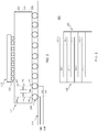
- FIG. 2 shows a simplified cross-sectional diagram of the die 120, the package 117, and the PCB 114 according to an embodiment of the present disclosure.
- the package 117 is mounted on the PCB 114, and the die 120 is mounted on the package 117.
- Electrical connections between the PCB 114 and the package 117 are provided by solder balls 220, and electrical connections between the package 117 and the die 120 are provided by bumps 215.
- the package 117 comprises a top layer 222, a bottom layer 226, and a center layer 224 between the top and bottom layers 222 and 226.
- the top and bottom layers 222 and 226 may each comprise one or more glass-epoxy materials (e.g., FR4), and the center layer 224 may comprise one or more ceramic materials.
- the center layer 224 may have a thickness that is greater than the thickness of each of the top and bottom layers 222 and 226.
- the center layer 224 may have a thickness (e.g., 60 ⁇ m) that is two to four times greater than the thickness (e.g., 20 ⁇ m) of each of the top and bottom layers 222 and 226.
- the package capacitor C pkg may be located within the center layer 224 of the package 117.
- the package capacitor C pkg may comprise a multilayer ceramic capacitor embedded in the center layer 224.
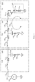
- FIG. 3 shows an example of a multilayer ceramic capacitor 305 that may be used for the package capacitor C pkg .
- the capacitor 305 comprises a first plurality of metal plates 320-1 to 320-4 coupled to a first metal terminal 310 of the capacitor 305, and a second plurality of metal plates 322-1 to 322-4 coupled to a second metal terminal 315 of the capacitor 305.
- the metal plates may comprise copper, nickel, silver, tantalum, and/or other type of metal. As shown in FIG.
- the first plurality of metal plates 320-1 to 320-4 are interlaced with the second plurality of metal plates 322-1 to 322-4.
- Each pair of adjacent metal plates may be separated by a ceramic layer (not shown) that acts as a dielectric layer between the metal plates.
- Each ceramic layer may comprise X5R, X7, Y5V and/or other ceramic material.
- the package 117 also includes vias 232 to 237 for providing conduction paths through the package 117.
- Each of the vias 232-237 may be formed by creating a hole in one or more layers of the package 117, and filling the hole with metal.
- the vias 232 to 237 have inductances and resistances contributing to the package inductance and package resistance discussed above.
- vias 232, 233 and 234 form a first conduction path through the bottom, center and top layers 226, 224 and 222, respectively, of the package 117.
- the first conduction path couples the power supply line 112 (e.g., metal trace) on the PCB 114 to the die 120.
- Via 232 of the first conduction path may be coupled to the power supply line 112 by one of the solder balls 220. It is to be appreciated that via 232 does not need to be aligned with the respective solder ball. For example, if via 232 is not aligned with the respective solder ball, then via 232 may be coupled to the respective solder ball by a metal trace (not shown) on or near the bottom surface of the package 117.
- Via 234 of the first conduction path may be coupled to the die 120 by one of the bumps 215. If via 234 is not aligned with the respective bump, then via 234 may be coupled to the respective bump by a metal trace (not shown) on or near the top surface of the package 117.
- Vias 235, 236 and 237 form a second conduction path through the bottom, center and top layers 226, 224 and 222, respectively, of the package 117.
- the second conduction path couples the ground line 212 (e.g., metal trace) on the PCB 114 to the die 120.
- Via 235 of the second conduction path may be coupled to the ground line by one of the solder balls 220. It is to be appreciated that via 235 does not need to be aligned with the respective solder ball. For example, if via 235 is not aligned with the respective solder ball, then via 235 may be coupled to the respective solder ball by a metal trace (not shown) on or near the bottom surface of the package 117.
- Via 237 of the second conduction path may be coupled to the die 120 by one of the bumps 215. If via 237 is not aligned with the respective bump, then via 237 may be coupled to the respective bump by a metal trace (not shown) on or near the top surface of the package 117.
- the first conductive path may be coupled to one of the terminals of the package capacitor C pkg
- the second conductive path may be coupled to the other terminal of the package capacitor C pkg
- the first conductive path may be coupled to one of the first and second metal terminals 310 and 315 of the capacitor 305
- the second conductive path may be coupled to the other one of the first and second metal terminals 310 and 315 of the capacitor 305.
- the package capacitor C pkg is coupled between the power supply 110 and the die 120.
- Inductance and capacitance in the PDN may cause the impedance of the PDN, as seen by the circuit 145, to peak at a certain frequency.
- a resistor-inductor-capacitor (RLC) loop 152 (also referred to as an RLC tank) may be formed by the package capacitor C pkg , package inductor 138, package resistor 136, grid resistor R grid , die capacitor C die and die resistor R die .
- the RLC loop 152 has two arrows indicating that current may flow in the RLC loop 152 in either direction.
- the impedance of the PDN as seen from the circuit 145, may peak at the resonant frequency of the RLC loop 152, as discussed further below.
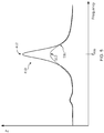
- FIG. 4 shows the impedance 410 of the PDN, as seen from the circuit 145, as a function of frequency.
- the impedance 410 peaks at the resonant frequency of the RLC loop 152 (denoted F res ).
- the impedance causes a voltage ripple on the power grid when the circuit 145 draws current from the PDN.
- the amplitude of the ripple is largest at the peak impedance 412, which may occur when the circuit 145 draws a time-varying current having a frequency at the resonant frequency of the RLC loop 152. It is desirable to minimize the amplitude of the ripple on the power grid to ensure that logic connected to the power grid functions properly, and therefore to minimize the peak impedance 412.
- the impedance 410 may also include a small local peak 415 due to an RLC loop associated with the board capacitor C PCB .
- the peak impedance 412 is controlled by the Q factor of the RLC loop 152, which is the ratio of the energy stored by the RLC loop 152 over the energy dissipated by the RLC loop 152.
- the lower the Q factor the lower the peak impedance.
- the Q factor is inversely proportional to the resistance of the RLC loop 152.
- the Q factor (and hence peak impedance 412) can be reduced by increasing the resistance of the RLC loop 152.
- One approach to increase the resistance of the RLC loop 152 is to increase the resistance of the grid resistor R grid .
- FIG. 5 shows the impedance 510 of the PDN in which the resistance of the grid resistor R grid has been increased compared to the impedance 410 in FIG. 4 .
- the impedance 510 with the higher grid resistance has a lower peak 512 at the resonant frequency.
- increasing the grid resistance has the undesirable effect of increasing the current-resistor (IR) voltage drop across the grid resistor R grid , which reduces the DC supply voltage at the circuit 145.
- the power supply 110 needs to output a higher supply voltage in order to achieve a given supply voltage at the circuit 145.
- Embodiments of the present disclosure provide a switchable package capacitor that allows the resistance of the RLC loop to be controlled to reduce the peak impedance of the PDN without increasing the IR drop between the power supply 110 and the circuit 145, as discussed further below.
- FIG. 6 shows a PDN according to an embodiment of the present disclosure.
- the die 620 comprises a resistor switch 615 (e.g., PMOS transistor switch) between the package capacitor C pkg and the circuit 145.
- the resistor switch 615 is included in the RLC loop 652 associated with the package capacitor C pkg .
- the resistance of the resistor switch 615 contributes to the resistance of the RLC loop 652, and can therefore be used to control the resistance of the RLC loop 652.
- the resistor switch 615 may have a programmable resistance and the die 620 may further include a resistance controller 625 for controlling the resistance of the resistor switch 615, and hence the resistance of the RLC loop 652.
- the resistance controller 625 may adjust the resistance of the resistor switch 615 to lower the Q factor of the RLC loop 652, and therefore reduce the peak impedance seen by the circuit 145.
- the resistance of the resistor switch 615 may be adjusted to increase the resistance of the RLC loop 652 to reduce the peak impedance without increasing the IR drop between the power supply 110 and the circuit 145. This is because the resistor switch 615 is located in a path 617 that is separate from the path between the power supply 110 and the circuit 145. As a result, the resistance of the resistor switch 615 does not contribute to the resistance between the power supply 110 and the circuit 145. Thus, the resistor switch 615 allows the resistance of the RLC loop 652 to be adjusted without negatively impacting the IR drop between the power supply 110 and the circuit 145, and thus without reducing the DC supply voltage at the circuit 145.
- package inductance between the power supply 110 and the die 620 is modeled as package inductor L pkg and package resistance between the power supply 110 and the die 620 is modeled as package resistor R pkg .
- package inductance and package resistance between the die 620 and the package capacitor C pkg are not shown in FIG. 6 for ease illustration. It is to be appreciated that the path 617 for the resistor switch 615 may be connected to the power grid at different locations, and is therefore not limited to the exemplary location shown in FIG. 6 .
- FIG. 7 shows a simplified cross-sectional diagram of the die 620, the package 617, and the PCB 114 according to an embodiment of the present disclosure.
- the package 617 is mounted on the PCB 114
- the die 620 is mounted on the package 617.
- Electrical connections between the PCB 114 and the package 617 are provided by solder balls 220, and electrical connections between the package 617 and the die 620 are provided by bumps 215.
- the package 617 in this embodiment differs from the package 117 in FIG. 2 in that the package capacitor C pkg is not coupled to the die 620 by the first and second conduction paths, which couple the power line 112 and the ground line 212 to the die 620. Instead, the package capacitor C pkg is coupled to the die 620 by separate conduction paths in the package 617.
- the package may include vias 733 to 736 for coupling the package capacitor C pkg to the die 620.
- Vias 733 and 734 form a third conduction path through the center and top layers 224 and 222, respectively, of the package 617.
- the third conduction path is used to couple a first terminal of the package capacitor C pkg to the die 620.
- via 733 may be coupled to the first terminal of the package capacitor C pkg and via 734 may be coupled to the die 620 by one of the bumps 215. If via 734 is not aligned with the respective bump, then via 734 may be coupled to the respective bump by a metal trace (not shown) on or near the top surface of the package 617.
- Vias 735 and 736 form a fourth conduction path through the center and top layers 224 and 222, respectively, of the package 617.
- the fourth conduction path is used to couple a second terminal of the package capacitor C pkg to the die 620.
- via 735 may be coupled to the second terminal of the package capacitor C pkg and via 736 may be coupled to the die 620 by one of the bumps 215. If via 736 is not aligned with the respective bump, then via 736 may be coupled to the respective bump by a metal trace (not shown) on or near the top surface of the package 617.
- the third conduction path in the package 617 may be used to couple the first terminal of the package capacitor C pkg to the resistor switch 615 on the die 620 and the fourth conduction path in the package 617 may be used to couple the second terminal of the package capacitor C pkg to a ground line on the die 620.
- the third conduction path may be used to couple the first terminal of the package capacitor C pkg to the ground line on the die 620 and the fourth conduction may be used to couple the second terminal of the package capacitor C pkg to the resistor switch 615 on the die 620.
- one of the first and second terminals of the package capacitor C pkg may be connected to the ground line 212 of the PCB 114 by a via (not shown) through the bottom layer 226 of the package 117 and one of the solder balls 220.
- the package capacitor C pkg may comprise a multilayer ceramic capacitor embedded in the center layer 224 of the package 617, and/or other type of capacitor.
- the package capacitor C pkg may be implemented with the multilayer ceramic capacitor 305 shown in FIG. 3 .
- the package capacitor C pkg is not limited to being located within the package 617.
- the package capacitor C pkg may be mounted on top of the package 617 next to the die 620.
- the package capacitor C pkg may be coupled to the die by metal traces on the package 617.
- the resistor switch 615 may have a programmable resistance for controlling the resistance of the RLC loop 652.
- FIG. 8 shows an exemplary implementation of the resistor switch 615 according to an embodiment of the present disclosure.
- the resistor switch 615 comprises a plurality of switches 815-1 to 815-n coupled in parallel.
- the resistance controller 625 controls the resistance of the resistor switch 615 by controlling the number of switches 815-1 to 815-n that are turned on. For example, the resistance controller 625 may reduce the resistance of the resistor switch 615 by turning on more of the switches 815-1 to 815-n, and may increase the resistance of the resistor switch 615 by turning on fewer of the switches 815-1 to 815-n.
- terminal 822 of the switch 615 may be coupled to the circuit 145 and terminal 825 of the resistor switch 615 may be coupled to the package capacitor C pkg .
- the granularity with which the resistance controller 625 can control the resistance of the resistor switch 615 may depend on the number of switches 815-1 to 815-n in the resistor switch 615. For example, the greater the number of switches 815-1 to 815-n in the resistor switch 615, the greater the granularity with which the resistance controller 625 can control the resistance of the resistor switch 615.
- each switch 815-1 to 815-n may comprise a PMOS transistor, as shown in FIG. 8 .
- the resistance controller 625 may turn on one of the switches 815-1 to 815-n by inputting a logic zero (low voltage) to the gate of the switch, and may turn off one of the switches 815-1 to 815-n by inputting a logic one (high voltage) to the gate of the switch.
- FIG. 9 shows impedance seen by the circuit 145 as a function of frequency for three different resistance settings of the resistors switch 615.
- impedance 410 is the impedance seen by the circuit 145 as a function of frequency when the resistance of the resistor switch 615 is low
- impedance 910 is the impedance seen by the circuit 145 as a function of frequency when the resistance of the resistor switch 615 is high
- Impedance 510 is the impedance seen by the circuit 145 as a function of frequency when the resistance of the resistor switch 615 is between the low and high resistances.
- the impedance 410 seen by the circuit 145 has a relatively large peak 412 at the resonant frequency of RLC loop 652.
- the impedance 510 seen by the circuit 145 has a smaller peak 512 at the resonant frequency. This is because increasing the resistance of the resistance switch 615 increases the resistance of the RLC loop 652. The increased resistance reduces the Q factor of the RLC loop 652, which in turn reduces the peak impedance 512 at the resonant frequency, as discussed above.
- the impedance at the resonant frequency may be further reduced by increasing resistance of the resistor switch 615.
- increasing the resistance of the resistor switch 615 further may cause the impedance seen by the circuit 145 to increase at lower frequencies. This is because increasing the resistance of the resistor switch 615 reduces the ability of the package capacitor C pkg to supply charge to the power grid to reduce voltage droops on the power grid.
- the resistance of the resistor switch 615 when the resistance of the resistor switch 615 is high, the impedance 910 seen by the circuit 145 has a larger peak 912 at lower frequencies, which can lead to higher voltage ripples on the power grid at lower frequencies. Accordingly, it may be desirable to tune the resistance of the resistor switch 615 to achieve a desired reduction in the peak impedance.
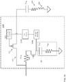
- FIG. 10 shows circuitry for tuning the resistance of the resistor switch 615 according an embodiment of the present disclosure.
- the circuitry includes a voltage detector 1030 and a test circuit 1040.
- the voltage detector 1030 is configured to measure the supply voltage at the circuit 145. To do this, the voltage detector 1030 may be coupled between the power-gating switch 140 and the circuit 145. Alternatively, the voltage detector 1030 may be coupled between the power-gating switch 140 and the power grid.
- the test circuit 1040 is configured to perform a procedure for tuning the resistance of the resistor switch 615.
- the circuit 145 may be coupled to the power supply 110 by the power-gating switch 140.
- the test circuit 1040 may then instruct the resistance controller 625 to sequentially set the resistance of the resistor switch 615 to each one of a plurality of different resistance values.
- the test circuit 1040 may determine the peak impedance across a frequency range based on voltage measurements from the voltage detector 1030.
- the test circuit 1040 may then select the resistance value corresponding to the lowest peak impedance.
- the test circuit 1040 may select any one of the resistance values corresponding to a peak impedance that is equal to or below a peak-impedance threshold.
- the peak-impedance threshold may be an impedance corresponding to a minimum supply voltage that is needed by one or more circuits on the die to function properly, as discussed further below.
- the test circuit 1040 may then instruct the resistance controller 625 to set the resistance of the switch resistor 615 to the selected resistance value.
- the peak impedance determined for each resistance value is not necessarily the absolute peak impedance for the resistance value.
- the impedance for a particular resistance value may be determined for each one of a plurality of different frequencies.
- the frequency at which the absolute peak impedance for the resistance value occurs may not exactly match one of the plurality of frequencies, in which case the determined peak impedance approximates the absolute peak impedance.
- the test circuit 1040 may determine the peak impedance for a particular resistance value according to the following procedure.
- the circuit 145 may be coupled to the power supply 110 by the power-gating switch 140 and operated across a frequency range of interest.
- the voltage detector 1030 may measure the supply voltage at the circuit 145 and output the resulting voltage measurements to the test circuit 1040.
- the test circuit 1040 may keep track of the minimum (smallest) measured voltage received from the voltage detector 1030.
- the test circuit 1040 may record the minimum measured voltage for the resistance value.
- the minimum measured voltage provides an indication of the peak impedance for the resistance value, in which a higher minimum measured voltage is indicative of a lower peak impedance and a lower minimum measured voltage is indicative of a higher peak impedance.
- the test circuit 1040 may repeat the above procedure for each resistance value to determine the minimum measured voltage for each resistance value. The test circuit 1040 may then select the resistance corresponding to the highest minimum measured voltage, and hence lowest peak impedance. Alternatively, the test circuit 1040 may select any one of the resistance values corresponding to a minimum measured voltage that is equal to or greater than a minimum-voltage threshold.
- the minimum-voltage threshold may correspond to a minimum supply voltage needed for one or more circuits on the die 620 to function properly. The test circuit 1040 may then instruct the resistance controller 625 to set the resistance of the resistor switch 615 to the selected resistance value.
- FIG. 11 shows an exemplary plot of the minimum measured voltage as a function of resistance of the resistor switch 615.
- the plot may be generated by having the resistance controller 625 sequentially set the resistance of the resistor switch 615 to each one of a plurality of different resistance values, and recording the minimum measured voltage for each resistance.
- the resistance of the resistor switch 615 is varied across a range bounded by a low resistance and a high resistance.
- the highest minimum measured voltage (and hence lowest peak impedance) occurs at an optimal resistance between the low and high resistances.
- the minimum measured voltages corresponding to the low resistance, optimal resistance, and high resistance are denoted low, optimal, and high, respectively.
- both the voltage detector 1030 and test circuit 1040 are located on the die 1020 in the example shown in FIG. 10 , it is to be appreciated that one of the voltage detector 1030 and test circuit 1040 may be external to the die 1020 or both of the voltage detector 1030 and test circuit 1040 may be external to the die 1020.
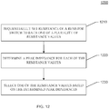
- FIG. 12 is a flow diagram illustrating a method 1200 for tuning the resistance of a resistor switch according to an embodiment of the present disclosure.
- the resistor switch e.g., resistor switch 615) may be on a die (e.g., die 620) and may be coupled between an external power line (e.g., power line 112) and an external capacitor (e.g., package capacitor C pkg ).
- the method 1200 may be performed by the voltage detector 1030 and the test circuit 1040.
- the resistance of the resistor switch is sequentially set to each one of a plurality of resistance values. This may be done, for example, by instructing a resistance controller (e.g., resistance controller 625) that controls the resistance of the resistor switch (e.g., resistor switch 615) to sequentially set the resistance of the resistor switch to each one of the resistance values.
- a resistance controller e.g., resistance controller 625 that controls the resistance of the resistor switch (e.g., resistor switch 615) to sequentially set the resistance of the resistor switch to each one of the resistance values.
- a peak impedance is determined for each one of the resistance values.
- the peak impedance for each resistor value may be determined by operating a circuit (e.g., circuit 145) coupled to the external power line across a frequency range, measuring a supply voltage of the circuit as the circuit is operated across the frequency range, and recording a minimum measured voltage.
- the minimum measured voltage for each resistance value may correspond to the peak impedance for the resistance value.
- one of the resistance values is selected based on the determined peak impedances. For example, the resistance value corresponding to a lowest one of the determined peak impedances may be selected. For the example in which the peak impedance for each resistance value is determined based on the minimum measured voltage for the resistance value, the resistance value corresponding to the highest minimum measured voltages may be selected. Alternatively, any one of the resistance values corresponding to a minimum measured voltage that is equal to or greater than a minimum-voltage threshold may be selected. The method may further include setting the resistance of the resistor switch to the selected resistance value.
- embodiments of the present disclosure allow the resistance of the resistor switch 615 to be tuned for a particular die.
- the ability to tune the resistance of the switch resistor 615 provides an advantage over using a fixed resistor (e.g., metal resistor) to control the resistance of the RLC loop 652.
- a fixed resistor e.g., metal resistor
- the resistance of a fixed resistor typically has to be determined before fabrication.
- the resistance of a metal resistor needs to be determined before fabrication in order to specify the dimensions of the metal resistor.
- the resistance needed to achieve a desired reduction in the peak impedance for a particular die may not be known until after the die has been fabricated due to process variations and/or other factors.
- the resistance of the fixed resistor may not achieve the desired reduction in the peak impedance.
- Embodiments of the present disclosure overcome the above drawbacks of using a fixed resistor. This is because the resistance of the resistor switch 615 can be tuned to a resistance value that achieves a desired reduction in the peak im
- FIG. 6 shows one power-gated circuit 145 for ease of illustration, it is to be appreciated that a die may include two or more power-gated circuits.
- FIG. 13 shows a die 1320 comprising a first power-gated circuit 1345a and a second power-gated circuit 1345b according to an embodiment of the present disclosure.
- the first and second circuits 1345a and 1345b may comprise first and second processors (e.g., central processing units (CPUs)) of a multi-core system on a chip (SoC).
- the first circuit 1345a has die capacitance modeled as die capacitor Ca die and resistance modeled as die resistor Ra die
- the second circuit 1345b has capacitance modeled as die capacitor Cb die and resistance modeled as die resistor Rb die ,
- the die 1320 also includes a power manager 1325 and first and second power-gating switches 1340a and 1340b.
- the first power-gating switch 1340a is coupled between the power grid and the first circuit 1345a
- the second power-gating switch 1340b is coupled between the power grid and the second circuit 1345b.
- the power manager 1325 is configured to manage power to each of the first and second circuits 1345a and 1345b by controlling the respective power-gating switch 1340a and 1340b.
- the power manager 1325 may connect the first circuit 1345a to the power grid when the first circuit 1345a is active by turning on the first power-gating switch 1340a, and may disconnect the first circuit 1345a from the power grid when the first circuit 1345a is inactive (e.g., idle) by turning off the first power-gating switch 1340a.
- the power manager 1325 may connect the second circuit 1345b to the power grid when the second circuit 1345b is active by turning on the second power-gating switch 1340b, and may disconnect the second circuit 1345b from the power grid when the second circuit 1345b is inactive (e.g., idle) by turning off the second power-gating switch 1340b.
- the power manager 1325 may independently control the first and second power-gating switches 1345a and 1345b, and therefore independently power gate the first and second circuits 1345a and 1345b.
- the power manager 1325 may independently power gate the first and second circuits 1345a and 1345b based on usage of the first and second circuits 1345a and 1345b.
- each power-gating switch 1345a and 1345b comprises a PMOS transistor.
- the power manager 1325 may turn on one of the power-gating switches 1345a and 1345b by driving the gate of the switch low, and may turn off one of the power-gating switches 1345a and 1345b by driving the gate of the switch high.
- the die 1320 includes the resistor switch 615 between the power grid and the package capacitor C pkg .
- the first circuit 1345a, the resistor switch 615 and the package capacitor C pkg form a first RLC loop 1352a
- the second circuit 1345b, the resistor switch 615 and the package capacitor C pkg form a second RLC loop 1352b.
- the first and second RLC loops 1352a and 1352b share the resistor switch 615.
- the resistor switch 615 may be used to adjust the resistance of each RLC loop 1352a and 1352b.
- the first and second RLC loops 1352a and 1352b may have different resistances. This is because the first and second circuits 1345a and 1345b connect to the power grid at different locations. As a result, the amount of grid resistance in each RLC loop is different.
- the grid resistance between the first and second circuits 1345a and 1345b is modeled as grid resistor R grid .
- the grid resistance between the first circuit 1345a and the resistor switch 615 and the grid resistance between the second circuit 1345b and the power supply 110 are not shown in FIG. 13 for ease of illustration.
- the peak impedance seen by each of the first and second circuits 1345a and 1345b may be minimized at a different resistance setting of the resistor switch 615.
- the resistance of the resistor switch 615 may be separately tuned for each of the first and second circuits 1345a and 1345b to determine a resistance value for each circuit.
- the first circuit 1345a may be connected to the power grid by the first power-gating switch 1340a with the second circuit 1345b disconnected from the power grid.
- the resistance of the resistor switch 615 may then be tuned by performing any one of the tuning procedures discussed above to determine a resistance value for the first circuit 1345a.
- the second circuit 1345b may be connected to the power grid by the second power-gating switch 1340b with the first circuit 1345a disconnected from the power grid.
- the resistance of the resistor switch 615 may then be tuned by performing any one of the tuning procedures discussed above to determine a resistance value for the second circuit 1345b.
- the resistance values for the first and second circuits 1345a and 1345b may be stored in memory on the die 1320.
- the resistance value for each circuit 1345a and 1345b may be determined based on the resistance value corresponding to the highest minimum measured voltage (and hence lowest peak impedance) for each circuit 1345a and 1345b.
- FIG. 14 shows minimum measured voltage 1410a as a function of resistance for the first circuit 1345a, and minimum measured voltage 1410b as a function of resistance for the second circuit 1345b.
- the highest minimum measured voltage (and hence lowest peak impedance) for the first circuit 1345a occurs at a resistance value of R a
- the highest minimum measured voltage (and hence lowest peak impedance) for the second circuit 1345b occurs at a resistance value of R b .
- the resistance value for the first circuit 1345a is R a and the resistance value for the second circuit 1345b is R b .
- the minimum measured voltages corresponding to resistance values R a and R b are denoted optimal(a) and optimal(b), respectively.
- a resistance value for the case where both circuits 1345a and 1345b are active may also be determined.
- the resistance value for this case may be a resistance value that is between (e.g., midway between) the resistance values for the first and second circuits 1345a and 1345b.
- the resistance value for this case may be a resistance value of R ab at which the minimum measured voltage for both circuits 1345a and 1345b is highest.
- the minimum measured voltage corresponding to the resistance value of R ab is denoted optimal(ab).
- the resistance controller 625 may set the resistance of the resistor switch 615 depending on the activity of the circuits 1345a and 1345b. For example, when the first circuit 1345a is active and the second circuit 1345b is inactive, the resistance controller 625 may set the resistance of the resistor switch 615 to the resistance value of R a . When the second circuit 1345b is active and the first circuit 1345a is inactive, the resistance controller 625 may set the resistance of the resistor switch 615 to the resistance value of R b . When both circuits 1345a and 1345b are active, the resistance controller 625 may set the resistance of the resistor switch 615 to the resistance value of R ab . In this example, the resistance controller 625 may receive a signal from the power manager 1325 indicating which circuits 1345a and 1345b are active at a given time.
- embodiments of the present disclosure are not limited to a die with two power-gated circuits, and may be implemented on a die with three or more power-gated circuits.
- embodiments of the present disclosure may be implemented on a die with three power-gated circuits labeled circuit A, circuit B and circuit C.
- a resistance value for each individual circuit may be determined.
- a resistance value may also be determined for each one of the following cases: circuits A and B are active and circuit C is inactive, circuits A and C are active and circuit B is inactive, circuits B and C are active and circuit A is inactive, and circuits A, B and C are all active.
- the resistance controller 625 may adjust the resistance of the resistor switch 615 according to the activity of the circuits. For example, if circuits A and B are active and circuit C in inactive, then the resistance controller 625 may set the resistance of the resistor switch 615 to the resistance value determined for the case where circuits A and B are active and circuit C is inactive. The resistance controller 625 may receive a signal from the power manager 1325 indicating the activity of the circuits at a given time.
- the resistance controller 625 may selectively disconnect the package capacitor C pkg from the power line 112 by opening the resistor switch 615. For example, the resistance controller 625 may disconnect the package capacitor C pkg from the power line 112 when the power line 112 is powered down and reconnect the package capacitor C pkg to the power line 112 after the power line 112 has been powered back on. This allows the package capacitor C pkg to retain charge when the power line 112 is powered down. As a result, when the power line 112 is powered back on, the amount of charge needed from the power supply 110 to recharge the package capacitor C pkg can be significantly reduced (assuming the package capacitor C pkg has low leakage). In contrast, when the power line 112 in FIG.
- the package capacitor C pkg is discharged (the voltage of the package capacitor C pkg collapses).
- the resistance controller 625 may receive a signal from the power manager 1325 indicating when the power line 112 is powered up and powered down.
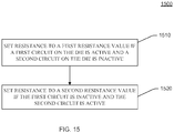
- FIG. 15 is a flow diagram illustrating a method 1500 for adjusting a resistance on a die according to an embodiment of the present disclosure.
- the resistance is between an external power line (e.g., power line 112) and an external capacitor (e.g., package capacitor C pkg ).
- the external power line may also refer to one or more conduction paths through the package 617 that couple power from the power supply 110 to the die 620.
- the resistance is set to a first resistance value if a first circuit on the die is active and a second circuit on the die is inactive.
- the resistance may be provided by a resistor switch (e.g., resistor switch 615) coupled between the external power line (e.g., power line 112) and the external capacitor (e.g., package capacitor C pkg ), and the resistance of the resistor switch may be set to the first resistance value.
- the resistance is set to a second resistance value if the first circuit is inactive and the second circuit is active.
- the resistance may be provided by the resistor switch, and the resistance of the resistor switch may be set to the second resistance value.
- the method 1500 may optionally include setting the resistance to a third resistance value if both the first and second circuits are active.
- the power manager 1325 may disconnect the first circuit 1345a from the power grid when the first circuit 1345a is inactive (e.g., idle) to reduce power leakage. The power manager 1325 does this by turning off the first power-gating switch 1340a. In the inactive state, the die capacitor Ca die of the first circuit 1345a is discharged. When the first circuit 1345a is needed, the power manager 1325 may reconnect the first circuit 1345a to the power grid by turning on the first power-gating switch 1340a. When the first power-gating switch 1340a is first turned on, the first circuit 1345a may consume a large amount of charge from the power grid to charge up the die capacitor Ca die . The transfer of charge causes the supply voltage at the power grid to droop.
- the power supply 110 is not able to supply charge fast enough to the power grid to prevent the droop due to the PDN inductance between the power supply 110 and the die 1320.
- the voltage droop can potentially cause circuit elements on the die 1320 to malfunction.
- the package capacitor C pkg may reduce the voltage droop by supplying some of the charge needed to charge up the die capacitor Ca die of the first circuit 1345a when the first power-gating switch 1340a is first turned on.
- the package capacitor C pkg supplies charge to the die capacitor Ca die through the resistor switch 615.
- the rate at which the package capacitor C pkg is able to transfer charge to the die capacitor Ca die and hence the ability of the package capacitor C pkg to reduce the voltage droop, depends on the resistance of the resistance switch 615.
- FIG. 16 shows two voltage curves 1610 and 1620 at the power grid for two different switch resistances, in which voltage curve 1610 corresponds to a lower switch resistance than voltage curve 1620.
- the first power-gating switch 1340a is turned on a time t0. Prior to time t0, the voltage at the power grid is approximately equal to the nominal supply voltage Vdd.
- the first power-gating switch 1340a is first turned on, the voltage at the power grid droops due to charge consumption by the die capacitor Ca die of the first circuit 1345a. As shown in FIG. 16 , the droop 1615 for voltage curve 1610 is smaller than the droop 1625 for voltage curve 1620.
- the package capacitor C pkg is able to supply charge to the die capacitor Ca die at a faster rate through the resistor switch 615, and therefore reduce the voltage droop by a greater amount.
- both voltage curves 1610 and 1620 oscillate at the resonant frequency of the RLC loop 1352a.
- the oscillations are dampened by the resistance of the resistor switch 615.
- the higher the switch resistance the more the oscillations are dampened.
- the oscillations die out faster for voltage curve 1620 compared with voltage curve 1610.
- each voltage curve 1610 and 1620 has a desirable property.
- Voltage curve 1610 has a smaller initial voltage droop than voltage curve 1620, while the oscillations of voltage curve 1620 are dampened out at a faster rate than voltage curve 1610.
- the resistance controller 625 dynamically adjusts the resistance of the resistance switch 615 during power up of the first circuit 1345a to achieve a voltage curve having the desirable properties of both voltage curves 1610 and 1620. More particularly, when the power-gating switch 1340a is first turned on, the resistance controller 625 may set the resistance of the resistance switch 615 to a first resistance value. After the initial voltage droop, the resistance controller 625 may set the resistance of the resistance switch 615 to a second resistance value, in which the second resistance value is greater than the first resistance value.
- the first resistance value allows the package capacitor C pkg to supply charge to the die capacitor Ca die faster (thereby reducing the initial voltage droop by a larger amount), while the second resistance value (which is greater than the first resistance value) dampens out oscillations at a faster rate.
- the resistance controller 625 may monitor the voltage at the power grid during power up of the first circuit 1345a, and dynamically adjust the resistance of the resistor switch 615 based on the detected voltage. For example, the resistance controller 625 may set the resistance of the switch resistor 615 to the first resistor value when the voltage at the power grid falls below a first voltage threshold, indicating the start of the initial voltage droop.
- the first voltage threshold may be a voltage that is slightly below the nominal supply voltage Vdd.
- the resistance controller 625 may then set the resistance of the switch resistor 615 to the second resistor value when the voltage at the power grid rises above a second voltage threshold, indicating that the initial voltage droop has passed.
- the second voltage threshold may be approximately equal to Vdd.
- the first and second voltage thresholds may have the same values or different values.
- the resistance controller 625 may set the resistance of the resistor switch 615 to the first resistance value during a time period between t0 and t1 to reduce the initial droop.
- FIG. 17 shows exemplary circuitry for dynamically adjusting the resistance of the resistor switch 615 during power up of the first circuit 1345a according to an embodiment of the present disclosure.
- the die 1720 includes a voltage detector 1730 coupled to the power grid.
- the voltage detector 1730 is configured to measure the voltage at the power grid and to output the measured voltage to the resistance controller 625.
- the power manager 1325 may send a signal to the resistance controller 625 indicating that the first circuit 1345a is about to be powered up.
- the resistance controller 625 may monitor the measured voltage from the voltage detector 1730. When the measured voltage falls below the first voltage threshold, the resistance controller 625 may set the resistance of the resistor switch 615 to the first resistance value. The resistance controller 625 may continue to monitor the measured voltage, and, when the measured voltage rises above the second voltage threshold, the resistance controller 625 may set the resistance of the resistor switch 615 to the second resistance value.
- the resistance controller 625 may set the resistance of the resistor switch 615 to the resistance value determined above for the active state (e.g., resistance value determined using the method 1200 in FIG. 12 ).
- the resistance controller 625 may set the resistance of the resistor switch 615 to the second resistance value after a predetermined time delay from the time that the resistance of the resistance switch 615 is set to the first resistance value.
- the time delay may be based on an estimation of the time duration of the initial voltage droop.
- FIG. 18 shows an exemplary implementation of the voltage detector 1730 according to an embodiment of the present disclosure.
- the voltage detector 1730 comprises an odd number of inverters 1830-1 to 1830-3 coupled in series, in which the output of the last inverter 1830-3 is coupled to the input of the first inverter 1830-1.
- the inverters 1830-1 to 1830-3 form a ring oscillator 1835, in which the oscillation frequency of the ring oscillator 1835 is a function of the delays of the inverters 1830-1 to 1830-3.
- the inverters 1830-1 to 1830-3 are biased by a voltage at the input 1810 of the voltage detector 1730, which is coupled to the power grid. Thus, the inverters 1830-1 to 1830-3 are biased by the voltage at the power grid.
- the delays of the inverters 1830-1 to 1830-3 are a function of the bias voltage of the inverters 1830-1 to 1830-3, and hence are a function of the voltage at the power grid. Since the oscillation frequency of the ring oscillator 835 is a function of the delays of the inverters 1830-1 to 1830-3, the oscillation frequency of the ring oscillator is a function of the voltage at the power grid, and may therefore be used to measure the voltage at the power grid.
- the voltage detector 1730 comprises a counter 1840 coupled to the ring oscillator 1835.
- the counter 1840 is configured to count the number of oscillations of the ring oscillator 1835 over a period of time, and output the count value to the resistance controller 625 at output 1820.
- the count value is a function of the oscillation frequency of the ring oscillator, and hence a function of the voltage at the power grid.
- the count value from the counter 1840 provides a measurement of the voltage at power grid.
- the resistance of the resistor switch 615 may also be dynamically adjusted during power up of the second circuit 1345b.
- the resistance controller 625 may monitor the voltage at the power grid during power up of the second circuit 1345b, and dynamically adjust the resistance of the resistor switch 615 based on the detected voltage in a manner similar to that described above for the first circuit 1345a.
- DSP digital signal processor
- ASIC application specific integrated circuit
- FPGA field programmable gate array
- a general-purpose processor may be a microprocessor, but in the alternative, the processor may be any conventional processor, controller, microcontroller, or state machine.
- a processor may also be implemented as a combination of computing devices, e.g., a combination of a DSP and a microprocessor, a plurality of microprocessors, one or more microprocessors in conjunction with a DSP core, or any other such configuration.
- a software module may reside in RAM memory, flash memory, ROM memory, EPROM memory, EEPROM memory, registers, hard disk, a removable disk, a CD-ROM, or any other form of storage medium known in the art.
- An exemplary storage medium is coupled to the processor such that the processor can read information from, and write information to, the storage medium.
- the storage medium may be integral to the processor.
- the processor and the storage medium may reside in an ASIC.
- the ASIC may reside in a user terminal.
- the processor and the storage medium may reside as discrete components in a user terminal.
- the functions described may be implemented in hardware, software, firmware, or any combination thereof. If implemented in software, the functions may be stored on or transmitted over as one or more instructions or code on a computer-readable medium.
- Computer-readable media includes both computer storage media and communication media including any medium that facilitates transfer of a computer program from one place to another.
- a storage media may be any available media that can be accessed by a general purpose or special purpose computer.
- such computer-readable media can comprise RAM, ROM, EEPROM, CD-ROM or other optical disk storage, magnetic disk storage or other magnetic storage devices, or any other medium that can be used to carry or store desired program code means in the form of instructions or data structures and that can be accessed by a general-purpose or special-purpose computer, or a general-purpose or special-purpose processor.
- any connection may be properly termed a computer-readable medium to the extent involving non-transient storage of transmitted signals.
- Disk and disc includes compact disc (CD), laser disc, optical disc, digital versatile disc (DVD), floppy disk and blu-ray disc where disks usually reproduce data magnetically, while discs reproduce data optically with lasers. Combinations of the above should also be included within the scope of computer-readable media.
Description
- Aspects of the present disclosure relate generally to package capacitors, and more particularly, to switchable package capacitors.
- A power distribution network (PDN) may be used to distribute power from a power supply (e.g., a battery) to various circuits on a die. Inductance and capacitance in the PDN may cause the impedance of the PDN, as seen by a circuit on the die, to peak at a resonant frequency of the PDN. The peak impedance may cause a large voltage ripple to appear on a power rail of the die when the circuit excites the resonant frequency of the PDN. The ripple may cause circuit elements on the die to malfunction.
- Attention is drawn to the document
US 2004/0183171 A1 , which provides a mechanism for delivering power to an on-die component (such as a buffer circuit). This may include a package unit having a low frequency delivery path and a high frequency delivery path and a die having the on-die component and a capacitive device each coupled in parallel between a first node and a second node. The die may further include a low frequency reception path and a high frequency reception path. The low frequency reception path may couple to the low frequency delivery path on the package unit and to the first node. The high frequency reception path may couple to the high frequency delivery path on the package unit and to the first node. The high frequency reception path may include a damping resistor - In accordance with the present invention, an apparatus and a method, as set forth in the independent claims, is provided. Embodiments of the invention are claimed in the dependent claims.
- The following presents a simplified summary of one or more embodiments in order to provide a basic understanding of such embodiments. This summary is not an extensive overview of all contemplated embodiments, and is intended to neither identify key or critical elements of all embodiments nor delineate the scope of any or all embodiments.
- Its sole purpose is to present some concepts of one or more embodiments in a simplified form as a prelude to the more detailed description that is presented later.
- According to a first aspect, an apparatus is described herein. The apparatus comprises a capacitor and a die. The die comprises a resistor switch coupled between a power line and the capacitor, wherein the resistor switch has an adjustable resistance, and the power line and the capacitor are both external to the die. The die also comprises a circuit configured to receive power from the power line.
- A second aspect relates to a method for adjusting a resistance on a die, wherein the resistance is between an external power line and an external capacitor. The method comprises setting the resistance to a first resistance value if a first circuit on the die is active and a second circuit on the die is inactive, and setting the resistance to a second resistance value if the first circuit is inactive and the second circuit is active.
- A third aspect relates to a method for tuning a resistance of a resistor switch on a die, wherein the resistor switch is coupled between an external power line and an external capacitor. The method comprises sequentially setting the resistance of the resistor switch to each one of a plurality of resistance values, and, for each resistance value, determining a peak impedance for the resistance value. The method also comprises selecting one of the resistance values based on the determined peak impedances.
- To the accomplishment of the foregoing and related ends, the one or more embodiments comprise the features hereinafter fully described and particularly pointed out in the claims. The following description and the annexed drawings set forth in detail certain illustrative aspects of the one or more embodiments. These aspects are indicative, however, of but a few of the various ways in which the principles of various embodiments may be employed and the described embodiments are intended to include all such aspects and their equivalents.
-
-
FIG. 1 shows an example of a power distribution network (PDN) for distributing power to one or more circuits on a die according to an embodiment of the present disclosure. -
FIG. 2 shows an example of a die and a package according to an embodiment of the present disclosure. -
FIG. 3 shows an example of a multilayer package capacitor according to an embodiment of the present disclosure. -
FIG. 4 is a plot showing impedance as a function of frequency according to an embodiment of the present disclosure. -
FIG. 5 is a plot showing impedance as a function of frequency for two different resistance values according to an embodiment of the present disclosure. -
FIG. 6 shows an example of a PDN comprising a switchable package capacitor according to an embodiment of the present disclosure. -
FIG. 7 shows a die and a package with a switchable package capacitor according to an embodiment of the present disclosure. -
FIG. 8 shows an exemplary implementation of a resistor switch according to an embodiment of the present disclosure. -
FIG. 9 is a plot showing impedance as a function of frequency for three different switch resistances according to an embodiment of the present disclosure. -
FIG. 10 shows circuitry for tuning the resistance of a resistor switch according to an embodiment of the present disclosure. -
FIG. 11 is a plot showing minimum measured voltage as a function of switch resistance according to an embodiment of the present disclosure. -
FIG. 12 is a flow diagram illustrating a method for tuning the resistance of a resistor switch according to an embodiment of the present disclosure. -
FIG. 13 shows a die comprising two circuits and a package comprising a switchable package capacitor according to an embodiment of the present disclosure. -
FIG. 14 is a plot showing minimum measured voltage as a function of switch resistance for different use cases according to an embodiment of the present disclosure. -
FIG. 15 is a flow diagram illustrating a method for adjusting a resistance on a die according to an embodiment of the present disclosure. -
FIG. 16 shows voltage droop for two different switch resistances according to an embodiment of the present disclosure. -
FIG. 17 shows circuitry for dynamically adjusting the resistance of a resistor switch during power up of a circuit according to an embodiment of the present disclosure. -
FIG. 18 shows an exemplary implementation of a voltage detector according to an embodiment of the present disclosure. - The detailed description set forth below, in connection with the appended drawings, is intended as a description of various configurations and is not intended to represent the only configurations in which the concepts described herein may be practiced. The detailed description includes specific details for the purpose of providing a thorough understanding of the various concepts. However, it will be apparent to those skilled in the art that these concepts may be practiced without these specific details. In some instances, well-known structures and components are shown in block diagram form in order to avoid obscuring such concepts.
- A power distribution network (PDN) is used to distribute power from a power supply (e.g., a battery) to various circuits on a die.
FIG. 1 shows an example of a PDN for supplying power from apower supply 110 to acircuit 145 on adie 120. The PDN supplies power to the die 120 via apower supply line 112 that traverses a printed circuit board (PCB) 114 and apackage 117. For ease of illustration, a ground line is not shown inFIG. 1 . The portion of the PDN corresponding to thePCB 114 may include board inductance modeled as board inductor LPCB and board resistance modeled as board resistor RPCB. The PDN may also include a board capacitor CPCB, which may have a small amount of inductance and resistance modeled asinductor 126 andresistor 124, respectively. - The portion of the PDN corresponding to the
package 117 may include package inductance and package resistance. The PDN may also include a package capacitor Cpkg, which may have a small amount of inductance and resistance modeled asinductor 134 andresistor 132, respectively. In one embodiment, the package capacitor CPkg is located within thepackage 117. As a result, a portion of the package inductance modeled asinductor 128 is located between thepower supply 110 and the package capacitor Cpkg, and another portion of the package inductance modeled asinductor 138 is located between the package capacitor Cpkg and thedie 120. Similarly, a portion of the package resistance modeled asresistor 130 is located between thepower supply 110 and the package capacitor Cpkg, and another portion of the package resistance modeled asresistor 136 is located between the package capacitor Cpkg and thedie 120. - The
die 120 includes a power grid for supplying power to thecircuit 145 from thepower supply 110. The power grid includes resistance modeled as grid resistor Rgrid inFIG. 1 . Thedie 120 also includes a power-gating switch 140 for power gating thecircuit 145. For example, the power-gating switch 140 may be configured to connect thecircuit 145 to the power grid when thecircuit 145 is active, and disconnect thecircuit 145 from the power grid when thecircuit 145 is inactive (e.g., idle) to conserve power. Thecircuit 145 has capacitance modeled as die capacitor Cdie and resistance modeled as die resistor Rdie, as shown inFIG. 1 . The capacitance of thecircuit 145 may include capacitances of transistors (e.g., metal-oxide-semiconductor field-effect transistors (MOSFETs)) in thecircuit 145 and parasitic-wire capacitances in thecircuit 145. The resistance of thecircuit 145 may include parasitic-wire resistances in thecircuit 145. - It is to be appreciated that
FIG. 1 is not intended to show all of the capacitances, inductances and/or resistances that may be present in the PDN. Rather,FIG. 1 is intended to show capacitances, inductances and resistances in the PDN that facilitate an understanding of embodiments of the present disclosure discussed below. -
FIG. 2 shows a simplified cross-sectional diagram of thedie 120, thepackage 117, and thePCB 114 according to an embodiment of the present disclosure. Thepackage 117 is mounted on thePCB 114, and thedie 120 is mounted on thepackage 117. Electrical connections between thePCB 114 and thepackage 117 are provided bysolder balls 220, and electrical connections between thepackage 117 and thedie 120 are provided bybumps 215. - In the example shown in
FIG. 2 , thepackage 117 comprises atop layer 222, abottom layer 226, and acenter layer 224 between the top andbottom layers bottom layers center layer 224 may comprise one or more ceramic materials. Thecenter layer 224 may have a thickness that is greater than the thickness of each of the top andbottom layers center layer 224 may have a thickness (e.g., 60 µm) that is two to four times greater than the thickness (e.g., 20 µm) of each of the top andbottom layers - As shown in
FIG. 2 , the package capacitor Cpkg may be located within thecenter layer 224 of thepackage 117. For example, the package capacitor Cpkg may comprise a multilayer ceramic capacitor embedded in thecenter layer 224. In this regard,FIG. 3 shows an example of a multilayerceramic capacitor 305 that may be used for the package capacitor Cpkg. Thecapacitor 305 comprises a first plurality of metal plates 320-1 to 320-4 coupled to afirst metal terminal 310 of thecapacitor 305, and a second plurality of metal plates 322-1 to 322-4 coupled to asecond metal terminal 315 of thecapacitor 305. The metal plates may comprise copper, nickel, silver, tantalum, and/or other type of metal. As shown inFIG. 3 , the first plurality of metal plates 320-1 to 320-4 are interlaced with the second plurality of metal plates 322-1 to 322-4. Each pair of adjacent metal plates may be separated by a ceramic layer (not shown) that acts as a dielectric layer between the metal plates. Each ceramic layer may comprise X5R, X7, Y5V and/or other ceramic material. - Returning to
FIG. 2 , thepackage 117 also includesvias 232 to 237 for providing conduction paths through thepackage 117. Each of the vias 232-237 may be formed by creating a hole in one or more layers of thepackage 117, and filling the hole with metal. Thevias 232 to 237 have inductances and resistances contributing to the package inductance and package resistance discussed above. - In the example shown in
FIG. 2 ,vias top layers package 117. The first conduction path couples the power supply line 112 (e.g., metal trace) on thePCB 114 to thedie 120. Via 232 of the first conduction path may be coupled to thepower supply line 112 by one of thesolder balls 220. It is to be appreciated that via 232 does not need to be aligned with the respective solder ball. For example, if via 232 is not aligned with the respective solder ball, then via 232 may be coupled to the respective solder ball by a metal trace (not shown) on or near the bottom surface of thepackage 117. Via 234 of the first conduction path may be coupled to the die 120 by one of thebumps 215. If via 234 is not aligned with the respective bump, then via 234 may be coupled to the respective bump by a metal trace (not shown) on or near the top surface of thepackage 117. -
Vias top layers package 117. The second conduction path couples the ground line 212 (e.g., metal trace) on thePCB 114 to thedie 120. Via 235 of the second conduction path may be coupled to the ground line by one of thesolder balls 220. It is to be appreciated that via 235 does not need to be aligned with the respective solder ball. For example, if via 235 is not aligned with the respective solder ball, then via 235 may be coupled to the respective solder ball by a metal trace (not shown) on or near the bottom surface of thepackage 117. Via 237 of the second conduction path may be coupled to the die 120 by one of thebumps 215. If via 237 is not aligned with the respective bump, then via 237 may be coupled to the respective bump by a metal trace (not shown) on or near the top surface of thepackage 117. - The first conductive path may be coupled to one of the terminals of the package capacitor Cpkg, and the second conductive path may be coupled to the other terminal of the package capacitor Cpkg. For the example where the package capacitor CPkg is implemented with the multilayer
ceramic capacitor 305, the first conductive path may be coupled to one of the first andsecond metal terminals capacitor 305, and the second conductive path may be coupled to the other one of the first andsecond metal terminals capacitor 305. In the example shown inFIG. 2 , the package capacitor Cpkg is coupled between thepower supply 110 and thedie 120. - Inductance and capacitance in the PDN may cause the impedance of the PDN, as seen by the
circuit 145, to peak at a certain frequency. For example, as shown inFIG. 1 , a resistor-inductor-capacitor (RLC) loop 152 (also referred to as an RLC tank) may be formed by the package capacitor Cpkg,package inductor 138,package resistor 136, grid resistor Rgrid, die capacitor Cdie and die resistor Rdie. InFIG. 1 , theRLC loop 152 has two arrows indicating that current may flow in theRLC loop 152 in either direction. TheRLC loop 152 causes the PDN to resonate at a resonant frequency given by:
RLC loop 152, and C is the capacitance of theRLC loop 152. The impedance of the PDN, as seen from thecircuit 145, may peak at the resonant frequency of theRLC loop 152, as discussed further below. -
FIG. 4 shows theimpedance 410 of the PDN, as seen from thecircuit 145, as a function of frequency. As shown inFIG. 4 , theimpedance 410 peaks at the resonant frequency of the RLC loop 152 (denoted Fres). The impedance causes a voltage ripple on the power grid when thecircuit 145 draws current from the PDN. The amplitude of the ripple is largest at thepeak impedance 412, which may occur when thecircuit 145 draws a time-varying current having a frequency at the resonant frequency of theRLC loop 152. It is desirable to minimize the amplitude of the ripple on the power grid to ensure that logic connected to the power grid functions properly, and therefore to minimize thepeak impedance 412. Theimpedance 410 may also include a smalllocal peak 415 due to an RLC loop associated with the board capacitor CPCB. - The
peak impedance 412 is controlled by the Q factor of theRLC loop 152, which is the ratio of the energy stored by theRLC loop 152 over the energy dissipated by theRLC loop 152. The lower the Q factor, the lower the peak impedance. The Q factor is inversely proportional to the resistance of theRLC loop 152. Thus, the Q factor (and hence peak impedance 412) can be reduced by increasing the resistance of theRLC loop 152. One approach to increase the resistance of theRLC loop 152 is to increase the resistance of the grid resistor Rgrid. In this regard,FIG. 5 shows theimpedance 510 of the PDN in which the resistance of the grid resistor Rgrid has been increased compared to theimpedance 410 inFIG. 4 . As shown inFIG. 5 , theimpedance 510 with the higher grid resistance has alower peak 512 at the resonant frequency. However, increasing the grid resistance has the undesirable effect of increasing the current-resistor (IR) voltage drop across the grid resistor Rgrid, which reduces the DC supply voltage at thecircuit 145. As a result, thepower supply 110 needs to output a higher supply voltage in order to achieve a given supply voltage at thecircuit 145. - Embodiments of the present disclosure provide a switchable package capacitor that allows the resistance of the RLC loop to be controlled to reduce the peak impedance of the PDN without increasing the IR drop between the
power supply 110 and thecircuit 145, as discussed further below. -
FIG. 6 shows a PDN according to an embodiment of the present disclosure. In this embodiment, thedie 620 comprises a resistor switch 615 (e.g., PMOS transistor switch) between the package capacitor Cpkg and thecircuit 145. Theresistor switch 615 is included in theRLC loop 652 associated with the package capacitor Cpkg. As a result, the resistance of theresistor switch 615 contributes to the resistance of theRLC loop 652, and can therefore be used to control the resistance of theRLC loop 652. In this regard, theresistor switch 615 may have a programmable resistance and thedie 620 may further include aresistance controller 625 for controlling the resistance of theresistor switch 615, and hence the resistance of theRLC loop 652. For example, theresistance controller 625 may adjust the resistance of theresistor switch 615 to lower the Q factor of theRLC loop 652, and therefore reduce the peak impedance seen by thecircuit 145. - The resistance of the
resistor switch 615 may be adjusted to increase the resistance of theRLC loop 652 to reduce the peak impedance without increasing the IR drop between thepower supply 110 and thecircuit 145. This is because theresistor switch 615 is located in apath 617 that is separate from the path between thepower supply 110 and thecircuit 145. As a result, the resistance of theresistor switch 615 does not contribute to the resistance between thepower supply 110 and thecircuit 145. Thus, theresistor switch 615 allows the resistance of theRLC loop 652 to be adjusted without negatively impacting the IR drop between thepower supply 110 and thecircuit 145, and thus without reducing the DC supply voltage at thecircuit 145. - In
FIG. 6 , package inductance between thepower supply 110 and thedie 620 is modeled as package inductor Lpkg and package resistance between thepower supply 110 and thedie 620 is modeled as package resistor Rpkg. Package inductance and package resistance between the die 620 and the package capacitor Cpkg are not shown inFIG. 6 for ease illustration. It is to be appreciated that thepath 617 for theresistor switch 615 may be connected to the power grid at different locations, and is therefore not limited to the exemplary location shown inFIG. 6 . -
FIG. 7 shows a simplified cross-sectional diagram of thedie 620, thepackage 617, and thePCB 114 according to an embodiment of the present disclosure. Thepackage 617 is mounted on thePCB 114, and thedie 620 is mounted on thepackage 617. Electrical connections between thePCB 114 and thepackage 617 are provided bysolder balls 220, and electrical connections between thepackage 617 and thedie 620 are provided bybumps 215. - The
package 617 in this embodiment differs from thepackage 117 inFIG. 2 in that the package capacitor Cpkg is not coupled to the die 620 by the first and second conduction paths, which couple thepower line 112 and theground line 212 to thedie 620. Instead, the package capacitor Cpkg is coupled to the die 620 by separate conduction paths in thepackage 617. - In this regard, the package may include
vias 733 to 736 for coupling the package capacitor Cpkg to thedie 620.Vias top layers package 617. The third conduction path is used to couple a first terminal of the package capacitor Cpkg to thedie 620. In this regard, via 733 may be coupled to the first terminal of the package capacitor Cpkg and via 734 may be coupled to the die 620 by one of thebumps 215. If via 734 is not aligned with the respective bump, then via 734 may be coupled to the respective bump by a metal trace (not shown) on or near the top surface of thepackage 617. -
Vias top layers package 617. The fourth conduction path is used to couple a second terminal of the package capacitor Cpkg to thedie 620. In this regard, via 735 may be coupled to the second terminal of the package capacitor Cpkg and via 736 may be coupled to the die 620 by one of thebumps 215. If via 736 is not aligned with the respective bump, then via 736 may be coupled to the respective bump by a metal trace (not shown) on or near the top surface of thepackage 617. - In this embodiment, the third conduction path in the
package 617 may be used to couple the first terminal of the package capacitor Cpkg to theresistor switch 615 on thedie 620 and the fourth conduction path in thepackage 617 may be used to couple the second terminal of the package capacitor Cpkg to a ground line on thedie 620. Alternately, the third conduction path may be used to couple the first terminal of the package capacitor Cpkg to the ground line on thedie 620 and the fourth conduction may be used to couple the second terminal of the package capacitor Cpkg to theresistor switch 615 on thedie 620. In another example, one of the first and second terminals of the package capacitor Cpkg may be connected to theground line 212 of thePCB 114 by a via (not shown) through thebottom layer 226 of thepackage 117 and one of thesolder balls 220. - The package capacitor Cpkg may comprise a multilayer ceramic capacitor embedded in the
center layer 224 of thepackage 617, and/or other type of capacitor. For example, the package capacitor Cpkg may be implemented with the multilayerceramic capacitor 305 shown inFIG. 3 . It is to be appreciated that the package capacitor Cpkg is not limited to being located within thepackage 617. For example, the package capacitor Cpkg may be mounted on top of thepackage 617 next to thedie 620. In this example, the package capacitor Cpkg may be coupled to the die by metal traces on thepackage 617. - As discussed above, the
resistor switch 615 may have a programmable resistance for controlling the resistance of theRLC loop 652. In this regard,FIG. 8 shows an exemplary implementation of theresistor switch 615 according to an embodiment of the present disclosure. In this embodiment, theresistor switch 615 comprises a plurality of switches 815-1 to 815-n coupled in parallel. Theresistance controller 625 controls the resistance of theresistor switch 615 by controlling the number of switches 815-1 to 815-n that are turned on. For example, theresistance controller 625 may reduce the resistance of theresistor switch 615 by turning on more of the switches 815-1 to 815-n, and may increase the resistance of theresistor switch 615 by turning on fewer of the switches 815-1 to 815-n. InFIG. 8 ,terminal 822 of theswitch 615 may be coupled to thecircuit 145 andterminal 825 of theresistor switch 615 may be coupled to the package capacitor Cpkg. - The granularity with which the
resistance controller 625 can control the resistance of theresistor switch 615 may depend on the number of switches 815-1 to 815-n in theresistor switch 615. For example, the greater the number of switches 815-1 to 815-n in theresistor switch 615, the greater the granularity with which theresistance controller 625 can control the resistance of theresistor switch 615. - In one embodiment, each switch 815-1 to 815-n may comprise a PMOS transistor, as shown in
FIG. 8 . In this embodiment, theresistance controller 625 may turn on one of the switches 815-1 to 815-n by inputting a logic zero (low voltage) to the gate of the switch, and may turn off one of the switches 815-1 to 815-n by inputting a logic one (high voltage) to the gate of the switch. -
FIG. 9 shows impedance seen by thecircuit 145 as a function of frequency for three different resistance settings of the resistors switch 615. In particular,impedance 410 is the impedance seen by thecircuit 145 as a function of frequency when the resistance of theresistor switch 615 is low, andimpedance 910 is the impedance seen by thecircuit 145 as a function of frequency when the resistance of theresistor switch 615 is high.Impedance 510 is the impedance seen by thecircuit 145 as a function of frequency when the resistance of theresistor switch 615 is between the low and high resistances. - As shown in
FIG. 9 , when the resistance of theresistor switch 615 is low, theimpedance 410 seen by thecircuit 145 has a relativelylarge peak 412 at the resonant frequency ofRLC loop 652. When the resistance of theresistor switch 615 is between the low and high resistances, theimpedance 510 seen by thecircuit 145 has asmaller peak 512 at the resonant frequency. This is because increasing the resistance of theresistance switch 615 increases the resistance of theRLC loop 652. The increased resistance reduces the Q factor of theRLC loop 652, which in turn reduces thepeak impedance 512 at the resonant frequency, as discussed above. - The impedance at the resonant frequency may be further reduced by increasing resistance of the
resistor switch 615. However, increasing the resistance of theresistor switch 615 further may cause the impedance seen by thecircuit 145 to increase at lower frequencies. This is because increasing the resistance of theresistor switch 615 reduces the ability of the package capacitor Cpkg to supply charge to the power grid to reduce voltage droops on the power grid. As a result, when the resistance of theresistor switch 615 is high, theimpedance 910 seen by thecircuit 145 has alarger peak 912 at lower frequencies, which can lead to higher voltage ripples on the power grid at lower frequencies. Accordingly, it may be desirable to tune the resistance of theresistor switch 615 to achieve a desired reduction in the peak impedance. - In this regard,
FIG. 10 shows circuitry for tuning the resistance of theresistor switch 615 according an embodiment of the present disclosure. The circuitry includes avoltage detector 1030 and atest circuit 1040. Thevoltage detector 1030 is configured to measure the supply voltage at thecircuit 145. To do this, thevoltage detector 1030 may be coupled between the power-gating switch 140 and thecircuit 145. Alternatively, thevoltage detector 1030 may be coupled between the power-gating switch 140 and the power grid. - The
test circuit 1040 is configured to perform a procedure for tuning the resistance of theresistor switch 615. In this regard, thecircuit 145 may be coupled to thepower supply 110 by the power-gating switch 140. Thetest circuit 1040 may then instruct theresistance controller 625 to sequentially set the resistance of theresistor switch 615 to each one of a plurality of different resistance values. For each resistance value, thetest circuit 1040 may determine the peak impedance across a frequency range based on voltage measurements from thevoltage detector 1030. Thetest circuit 1040 may then select the resistance value corresponding to the lowest peak impedance. Alternatively, thetest circuit 1040 may select any one of the resistance values corresponding to a peak impedance that is equal to or below a peak-impedance threshold. The peak-impedance threshold may be an impedance corresponding to a minimum supply voltage that is needed by one or more circuits on the die to function properly, as discussed further below. Thetest circuit 1040 may then instruct theresistance controller 625 to set the resistance of theswitch resistor 615 to the selected resistance value. - It is to be appreciated that the peak impedance determined for each resistance value is not necessarily the absolute peak impedance for the resistance value. For example, the impedance for a particular resistance value may be determined for each one of a plurality of different frequencies. In this example, the frequency at which the absolute peak impedance for the resistance value occurs may not exactly match one of the plurality of frequencies, in which case the determined peak impedance approximates the absolute peak impedance.
- The
test circuit 1040 may determine the peak impedance for a particular resistance value according to the following procedure. In this regard, thecircuit 145 may be coupled to thepower supply 110 by the power-gating switch 140 and operated across a frequency range of interest. As thecircuit 145 is operated across the frequency range, thevoltage detector 1030 may measure the supply voltage at thecircuit 145 and output the resulting voltage measurements to thetest circuit 1040. Thetest circuit 1040 may keep track of the minimum (smallest) measured voltage received from thevoltage detector 1030. After thecircuit 145 completes operations across the frequency range, thetest circuit 1040 may record the minimum measured voltage for the resistance value. The minimum measured voltage provides an indication of the peak impedance for the resistance value, in which a higher minimum measured voltage is indicative of a lower peak impedance and a lower minimum measured voltage is indicative of a higher peak impedance. - The
test circuit 1040 may repeat the above procedure for each resistance value to determine the minimum measured voltage for each resistance value. Thetest circuit 1040 may then select the resistance corresponding to the highest minimum measured voltage, and hence lowest peak impedance. Alternatively, thetest circuit 1040 may select any one of the resistance values corresponding to a minimum measured voltage that is equal to or greater than a minimum-voltage threshold. The minimum-voltage threshold may correspond to a minimum supply voltage needed for one or more circuits on thedie 620 to function properly. Thetest circuit 1040 may then instruct theresistance controller 625 to set the resistance of theresistor switch 615 to the selected resistance value. -
FIG. 11 shows an exemplary plot of the minimum measured voltage as a function of resistance of theresistor switch 615. For example, the plot may be generated by having theresistance controller 625 sequentially set the resistance of theresistor switch 615 to each one of a plurality of different resistance values, and recording the minimum measured voltage for each resistance. In the example shown inFIG. 11 , the resistance of theresistor switch 615 is varied across a range bounded by a low resistance and a high resistance. The highest minimum measured voltage (and hence lowest peak impedance) occurs at an optimal resistance between the low and high resistances. InFIG. 11 , the minimum measured voltages corresponding to the low resistance, optimal resistance, and high resistance are denoted low, optimal, and high, respectively. - Although both the
voltage detector 1030 andtest circuit 1040 are located on thedie 1020 in the example shown inFIG. 10 , it is to be appreciated that one of thevoltage detector 1030 andtest circuit 1040 may be external to thedie 1020 or both of thevoltage detector 1030 andtest circuit 1040 may be external to thedie 1020. -
FIG. 12 is a flow diagram illustrating amethod 1200 for tuning the resistance of a resistor switch according to an embodiment of the present disclosure. The resistor switch (e.g., resistor switch 615) may be on a die (e.g., die 620) and may be coupled between an external power line (e.g., power line 112) and an external capacitor (e.g., package capacitor Cpkg). Themethod 1200 may be performed by thevoltage detector 1030 and thetest circuit 1040. - In
step 1210, the resistance of the resistor switch is sequentially set to each one of a plurality of resistance values. This may be done, for example, by instructing a resistance controller (e.g., resistance controller 625) that controls the resistance of the resistor switch (e.g., resistor switch 615) to sequentially set the resistance of the resistor switch to each one of the resistance values. - In
step 1220, a peak impedance is determined for each one of the resistance values. For example, the peak impedance for each resistor value may be determined by operating a circuit (e.g., circuit 145) coupled to the external power line across a frequency range, measuring a supply voltage of the circuit as the circuit is operated across the frequency range, and recording a minimum measured voltage. In this example, the minimum measured voltage for each resistance value may correspond to the peak impedance for the resistance value. - In
step 1230, one of the resistance values is selected based on the determined peak impedances. For example, the resistance value corresponding to a lowest one of the determined peak impedances may be selected. For the example in which the peak impedance for each resistance value is determined based on the minimum measured voltage for the resistance value, the resistance value corresponding to the highest minimum measured voltages may be selected. Alternatively, any one of the resistance values corresponding to a minimum measured voltage that is equal to or greater than a minimum-voltage threshold may be selected. The method may further include setting the resistance of the resistor switch to the selected resistance value. - Thus, embodiments of the present disclosure allow the resistance of the
resistor switch 615 to be tuned for a particular die. The ability to tune the resistance of theswitch resistor 615 provides an advantage over using a fixed resistor (e.g., metal resistor) to control the resistance of theRLC loop 652. This is because the resistance of a fixed resistor typically has to be determined before fabrication. For example, the resistance of a metal resistor needs to be determined before fabrication in order to specify the dimensions of the metal resistor. However, the resistance needed to achieve a desired reduction in the peak impedance for a particular die may not be known until after the die has been fabricated due to process variations and/or other factors. As a result, the resistance of the fixed resistor may not achieve the desired reduction in the peak impedance. Embodiments of the present disclosure overcome the above drawbacks of using a fixed resistor. This is because the resistance of theresistor switch 615 can be tuned to a resistance value that achieves a desired reduction in the peak impedance for a particular die after fabrication. - Although
FIG. 6 shows one power-gatedcircuit 145 for ease of illustration, it is to be appreciated that a die may include two or more power-gated circuits. In this regard,FIG. 13 shows adie 1320 comprising a first power-gatedcircuit 1345a and a second power-gatedcircuit 1345b according to an embodiment of the present disclosure. For example, the first andsecond circuits first circuit 1345a has die capacitance modeled as die capacitor Cadie and resistance modeled as die resistor Radie, and thesecond circuit 1345b has capacitance modeled as die capacitor Cbdie and resistance modeled as die resistor Rbdie, - The
die 1320 also includes apower manager 1325 and first and second power-gating switches gating switch 1340a is coupled between the power grid and thefirst circuit 1345a, and the second power-gating switch 1340b is coupled between the power grid and thesecond circuit 1345b. Thepower manager 1325 is configured to manage power to each of the first andsecond circuits gating switch power manager 1325 may connect thefirst circuit 1345a to the power grid when thefirst circuit 1345a is active by turning on the first power-gating switch 1340a, and may disconnect thefirst circuit 1345a from the power grid when thefirst circuit 1345a is inactive (e.g., idle) by turning off the first power-gating switch 1340a. Similarly, thepower manager 1325 may connect thesecond circuit 1345b to the power grid when thesecond circuit 1345b is active by turning on the second power-gating switch 1340b, and may disconnect thesecond circuit 1345b from the power grid when thesecond circuit 1345b is inactive (e.g., idle) by turning off the second power-gating switch 1340b. - The
power manager 1325 may independently control the first and second power-gating switches second circuits power manager 1325 may independently power gate the first andsecond circuits second circuits FIG. 13 , each power-gating switch power manager 1325 may turn on one of the power-gating switches gating switches - The
die 1320 includes theresistor switch 615 between the power grid and the package capacitor Cpkg. In the example shown inFIG. 13 , thefirst circuit 1345a, theresistor switch 615 and the package capacitor Cpkg form afirst RLC loop 1352a, and thesecond circuit 1345b, theresistor switch 615 and the package capacitor Cpkg form asecond RLC loop 1352b. The first andsecond RLC loops resistor switch 615. Thus, theresistor switch 615 may be used to adjust the resistance of eachRLC loop - Although the first and
second RLC loops resistor switch 615, the first andsecond RLC loops second circuits FIG. 13 , the grid resistance between the first andsecond circuits first circuit 1345a and theresistor switch 615 and the grid resistance between thesecond circuit 1345b and thepower supply 110 are not shown inFIG. 13 for ease of illustration. - Because the first and
second RLC loops second circuits resistor switch 615. In this regard, the resistance of theresistor switch 615 may be separately tuned for each of the first andsecond circuits - For example, the
first circuit 1345a may be connected to the power grid by the first power-gating switch 1340a with thesecond circuit 1345b disconnected from the power grid. The resistance of theresistor switch 615 may then be tuned by performing any one of the tuning procedures discussed above to determine a resistance value for thefirst circuit 1345a. Similarly, thesecond circuit 1345b may be connected to the power grid by the second power-gating switch 1340b with thefirst circuit 1345a disconnected from the power grid. The resistance of theresistor switch 615 may then be tuned by performing any one of the tuning procedures discussed above to determine a resistance value for thesecond circuit 1345b. The resistance values for the first andsecond circuits die 1320. - In one embodiment, the resistance value for each
circuit circuit FIG. 14 shows minimum measuredvoltage 1410a as a function of resistance for thefirst circuit 1345a, and minimum measuredvoltage 1410b as a function of resistance for thesecond circuit 1345b. As shown inFIG. 14 , the highest minimum measured voltage (and hence lowest peak impedance) for thefirst circuit 1345a occurs at a resistance value of Ra, and the highest minimum measured voltage (and hence lowest peak impedance) for thesecond circuit 1345b occurs at a resistance value of Rb. Thus, in this example, the resistance value for thefirst circuit 1345a is Ra and the resistance value for thesecond circuit 1345b is Rb. InFIG. 14 , the minimum measured voltages corresponding to resistance values Ra and Rb are denoted optimal(a) and optimal(b), respectively. - A resistance value for the case where both
circuits second circuits FIG. 14 , in another example, the resistance value for this case may be a resistance value of Rab at which the minimum measured voltage for bothcircuits FIG. 14 , the minimum measured voltage corresponding to the resistance value of Rab is denoted optimal(ab). - After the resistance values for the different use cases have been determined, the
resistance controller 625 may set the resistance of theresistor switch 615 depending on the activity of thecircuits first circuit 1345a is active and thesecond circuit 1345b is inactive, theresistance controller 625 may set the resistance of theresistor switch 615 to the resistance value of Ra. When thesecond circuit 1345b is active and thefirst circuit 1345a is inactive, theresistance controller 625 may set the resistance of theresistor switch 615 to the resistance value of Rb. When bothcircuits resistance controller 625 may set the resistance of theresistor switch 615 to the resistance value of Rab. In this example, theresistance controller 625 may receive a signal from thepower manager 1325 indicating whichcircuits - It is to be appreciated that embodiments of the present disclosure are not limited to a die with two power-gated circuits, and may be implemented on a die with three or more power-gated circuits. For example, embodiments of the present disclosure may be implemented on a die with three power-gated circuits labeled circuit A, circuit B and circuit C. In this example, a resistance value for each individual circuit may be determined. A resistance value may also be determined for each one of the following cases: circuits A and B are active and circuit C is inactive, circuits A and C are active and circuit B is inactive, circuits B and C are active and circuit A is inactive, and circuits A, B and C are all active. In this example, after the resistance values for the different cases are determined, the
resistance controller 625 may adjust the resistance of theresistor switch 615 according to the activity of the circuits. For example, if circuits A and B are active and circuit C in inactive, then theresistance controller 625 may set the resistance of theresistor switch 615 to the resistance value determined for the case where circuits A and B are active and circuit C is inactive. Theresistance controller 625 may receive a signal from thepower manager 1325 indicating the activity of the circuits at a given time. - In one embodiment, the
resistance controller 625 may selectively disconnect the package capacitor Cpkg from thepower line 112 by opening theresistor switch 615. For example, theresistance controller 625 may disconnect the package capacitor Cpkg from thepower line 112 when thepower line 112 is powered down and reconnect the package capacitor Cpkg to thepower line 112 after thepower line 112 has been powered back on. This allows the package capacitor Cpkg to retain charge when thepower line 112 is powered down. As a result, when thepower line 112 is powered back on, the amount of charge needed from thepower supply 110 to recharge the package capacitor Cpkg can be significantly reduced (assuming the package capacitor Cpkg has low leakage). In contrast, when thepower line 112 inFIG. 1 is powered down, the package capacitor Cpkg is discharged (the voltage of the package capacitor Cpkg collapses). In this embodiment, theresistance controller 625 may receive a signal from thepower manager 1325 indicating when thepower line 112 is powered up and powered down. -
FIG. 15 is a flow diagram illustrating amethod 1500 for adjusting a resistance on a die according to an embodiment of the present disclosure. The resistance is between an external power line (e.g., power line 112) and an external capacitor (e.g., package capacitor Cpkg). The external power line may also refer to one or more conduction paths through thepackage 617 that couple power from thepower supply 110 to thedie 620. - In
step 1510, the resistance is set to a first resistance value if a first circuit on the die is active and a second circuit on the die is inactive. For example, the resistance may be provided by a resistor switch (e.g., resistor switch 615) coupled between the external power line (e.g., power line 112) and the external capacitor (e.g., package capacitor Cpkg), and the resistance of the resistor switch may be set to the first resistance value. - In
step 1520, the resistance is set to a second resistance value if the first circuit is inactive and the second circuit is active. For example, the resistance may be provided by the resistor switch, and the resistance of the resistor switch may be set to the second resistance value. Themethod 1500 may optionally include setting the resistance to a third resistance value if both the first and second circuits are active. - As discussed above, the
power manager 1325 may disconnect thefirst circuit 1345a from the power grid when thefirst circuit 1345a is inactive (e.g., idle) to reduce power leakage. Thepower manager 1325 does this by turning off the first power-gating switch 1340a. In the inactive state, the die capacitor Cadie of thefirst circuit 1345a is discharged. When thefirst circuit 1345a is needed, thepower manager 1325 may reconnect thefirst circuit 1345a to the power grid by turning on the first power-gating switch 1340a. When the first power-gating switch 1340a is first turned on, thefirst circuit 1345a may consume a large amount of charge from the power grid to charge up the die capacitor Cadie. The transfer of charge causes the supply voltage at the power grid to droop. This is because thepower supply 110 is not able to supply charge fast enough to the power grid to prevent the droop due to the PDN inductance between thepower supply 110 and thedie 1320. The voltage droop can potentially cause circuit elements on thedie 1320 to malfunction. - The package capacitor Cpkg may reduce the voltage droop by supplying some of the charge needed to charge up the die capacitor Cadie of the
first circuit 1345a when the first power-gating switch 1340a is first turned on. The package capacitor Cpkg supplies charge to the die capacitor Cadie through theresistor switch 615. As a result, the rate at which the package capacitor Cpkg is able to transfer charge to the die capacitor Cadie, and hence the ability of the package capacitor Cpkg to reduce the voltage droop, depends on the resistance of theresistance switch 615. - In this regard,
FIG. 16 shows twovoltage curves 1610 and 1620 at the power grid for two different switch resistances, in whichvoltage curve 1610 corresponds to a lower switch resistance than voltage curve 1620. InFIG. 16 , the first power-gating switch 1340a is turned on a time t0. Prior to time t0, the voltage at the power grid is approximately equal to the nominal supply voltage Vdd. When the first power-gating switch 1340a is first turned on, the voltage at the power grid droops due to charge consumption by the die capacitor Cadie of thefirst circuit 1345a. As shown inFIG. 16 , thedroop 1615 forvoltage curve 1610 is smaller than thedroop 1625 for voltage curve 1620. This is because the switch resistance is lower forvoltage curve 1610. As a result, the package capacitor Cpkg is able to supply charge to the die capacitor Cadie at a faster rate through theresistor switch 615, and therefore reduce the voltage droop by a greater amount. - As also shown in
FIG. 16 , bothvoltage curves 1610 and 1620 oscillate at the resonant frequency of theRLC loop 1352a. The oscillations are dampened by the resistance of theresistor switch 615. The higher the switch resistance, the more the oscillations are dampened. As a result, the oscillations die out faster for voltage curve 1620 compared withvoltage curve 1610. - Thus, each
voltage curve 1610 and 1620 has a desirable property.Voltage curve 1610 has a smaller initial voltage droop than voltage curve 1620, while the oscillations of voltage curve 1620 are dampened out at a faster rate thanvoltage curve 1610. - In one embodiment, the
resistance controller 625 dynamically adjusts the resistance of theresistance switch 615 during power up of thefirst circuit 1345a to achieve a voltage curve having the desirable properties of bothvoltage curves 1610 and 1620. More particularly, when the power-gating switch 1340a is first turned on, theresistance controller 625 may set the resistance of theresistance switch 615 to a first resistance value. After the initial voltage droop, theresistance controller 625 may set the resistance of theresistance switch 615 to a second resistance value, in which the second resistance value is greater than the first resistance value. The first resistance value allows the package capacitor Cpkg to supply charge to the die capacitor Cadie faster (thereby reducing the initial voltage droop by a larger amount), while the second resistance value (which is greater than the first resistance value) dampens out oscillations at a faster rate. - In one embodiment, the
resistance controller 625 may monitor the voltage at the power grid during power up of thefirst circuit 1345a, and dynamically adjust the resistance of theresistor switch 615 based on the detected voltage. For example, theresistance controller 625 may set the resistance of theswitch resistor 615 to the first resistor value when the voltage at the power grid falls below a first voltage threshold, indicating the start of the initial voltage droop. The first voltage threshold may be a voltage that is slightly below the nominal supply voltage Vdd. Theresistance controller 625 may then set the resistance of theswitch resistor 615 to the second resistor value when the voltage at the power grid rises above a second voltage threshold, indicating that the initial voltage droop has passed. The second voltage threshold may be approximately equal to Vdd. The first and second voltage thresholds may have the same values or different values. In the example shown inFIG. 16 , theresistance controller 625 may set the resistance of theresistor switch 615 to the first resistance value during a time period between t0 and t1 to reduce the initial droop. -
FIG. 17 shows exemplary circuitry for dynamically adjusting the resistance of theresistor switch 615 during power up of thefirst circuit 1345a according to an embodiment of the present disclosure. In this embodiment, thedie 1720 includes avoltage detector 1730 coupled to the power grid. Thevoltage detector 1730 is configured to measure the voltage at the power grid and to output the measured voltage to theresistance controller 625. - When the
first circuit 1345a is to be powered up from an inactive state to an active state, thepower manager 1325 may send a signal to theresistance controller 625 indicating that thefirst circuit 1345a is about to be powered up. In response, theresistance controller 625 may monitor the measured voltage from thevoltage detector 1730. When the measured voltage falls below the first voltage threshold, theresistance controller 625 may set the resistance of theresistor switch 615 to the first resistance value. Theresistance controller 625 may continue to monitor the measured voltage, and, when the measured voltage rises above the second voltage threshold, theresistance controller 625 may set the resistance of theresistor switch 615 to the second resistance value. After the oscillations have been sufficiently reduced to begin active operation of thefirst circuit 1345a, theresistance controller 625 may set the resistance of theresistor switch 615 to the resistance value determined above for the active state (e.g., resistance value determined using themethod 1200 inFIG. 12 ). - Alternatively, the
resistance controller 625 may set the resistance of theresistor switch 615 to the second resistance value after a predetermined time delay from the time that the resistance of theresistance switch 615 is set to the first resistance value. The time delay may be based on an estimation of the time duration of the initial voltage droop. -
FIG. 18 shows an exemplary implementation of thevoltage detector 1730 according to an embodiment of the present disclosure. In this embodiment, thevoltage detector 1730 comprises an odd number of inverters 1830-1 to 1830-3 coupled in series, in which the output of the last inverter 1830-3 is coupled to the input of the first inverter 1830-1. As a result, the inverters 1830-1 to 1830-3 form aring oscillator 1835, in which the oscillation frequency of thering oscillator 1835 is a function of the delays of the inverters 1830-1 to 1830-3. - The inverters 1830-1 to 1830-3 are biased by a voltage at the
input 1810 of thevoltage detector 1730, which is coupled to the power grid. Thus, the inverters 1830-1 to 1830-3 are biased by the voltage at the power grid. The delays of the inverters 1830-1 to 1830-3 are a function of the bias voltage of the inverters 1830-1 to 1830-3, and hence are a function of the voltage at the power grid. Since the oscillation frequency of the ring oscillator 835 is a function of the delays of the inverters 1830-1 to 1830-3, the oscillation frequency of the ring oscillator is a function of the voltage at the power grid, and may therefore be used to measure the voltage at the power grid. - In this regard, the
voltage detector 1730 comprises acounter 1840 coupled to thering oscillator 1835. Thecounter 1840 is configured to count the number of oscillations of thering oscillator 1835 over a period of time, and output the count value to theresistance controller 625 atoutput 1820. The count value is a function of the oscillation frequency of the ring oscillator, and hence a function of the voltage at the power grid. Thus, the count value from thecounter 1840 provides a measurement of the voltage at power grid. - It is to be appreciated that the resistance of the
resistor switch 615 may also be dynamically adjusted during power up of thesecond circuit 1345b. For example, theresistance controller 625 may monitor the voltage at the power grid during power up of thesecond circuit 1345b, and dynamically adjust the resistance of theresistor switch 615 based on the detected voltage in a manner similar to that described above for thefirst circuit 1345a. - Those skilled in the art would appreciate that the various illustrative logical blocks, modules, circuits, and algorithm steps described in connection with the disclosure herein may be implemented as electronic hardware, computer software, or combinations of both. To clearly illustrate this interchangeability of hardware and software, various illustrative components, blocks, modules, circuits, and steps have been described above generally in terms of their functionality. Whether such functionality is implemented as hardware or software depends upon the particular application and design constraints imposed on the overall system. Skilled artisans may implement the described functionality in varying ways for each particular application, but such implementation decisions should not be interpreted as causing a departure from the scope of the present disclosure.
- The various illustrative logical blocks, modules, and circuits described in connection with the disclosure herein may be implemented or performed with a general-purpose processor, a digital signal processor (DSP), an application specific integrated circuit (ASIC), a field programmable gate array (FPGA) or other programmable logic device, discrete gate or transistor logic, discrete hardware components, or any combination thereof designed to perform the functions described herein. A general-purpose processor may be a microprocessor, but in the alternative, the processor may be any conventional processor, controller, microcontroller, or state machine. A processor may also be implemented as a combination of computing devices, e.g., a combination of a DSP and a microprocessor, a plurality of microprocessors, one or more microprocessors in conjunction with a DSP core, or any other such configuration.
- The steps of a method or algorithm described in connection with the disclosure herein may be embodied directly in hardware, in a software module executed by a processor, or in a combination of the two. A software module may reside in RAM memory, flash memory, ROM memory, EPROM memory, EEPROM memory, registers, hard disk, a removable disk, a CD-ROM, or any other form of storage medium known in the art. An exemplary storage medium is coupled to the processor such that the processor can read information from, and write information to, the storage medium. In the alternative, the storage medium may be integral to the processor. The processor and the storage medium may reside in an ASIC. The ASIC may reside in a user terminal. In the alternative, the processor and the storage medium may reside as discrete components in a user terminal.
- In one or more exemplary designs, the functions described may be implemented in hardware, software, firmware, or any combination thereof. If implemented in software, the functions may be stored on or transmitted over as one or more instructions or code on a computer-readable medium. Computer-readable media includes both computer storage media and communication media including any medium that facilitates transfer of a computer program from one place to another. A storage media may be any available media that can be accessed by a general purpose or special purpose computer. By way of example, and not limitation, such computer-readable media can comprise RAM, ROM, EEPROM, CD-ROM or other optical disk storage, magnetic disk storage or other magnetic storage devices, or any other medium that can be used to carry or store desired program code means in the form of instructions or data structures and that can be accessed by a general-purpose or special-purpose computer, or a general-purpose or special-purpose processor. Also, any connection may be properly termed a computer-readable medium to the extent involving non-transient storage of transmitted signals. For example, if the software is transmitted from a website, server, or other remote source using a coaxial cable, fiber optic cable, twisted pair, digital subscriber line (DSL), or wireless technologies such as infrared, radio, and microwave, then the coaxial cable, fiber optic cable, twisted pair, DSL, or wireless technologies such as infrared, radio, and microwave are included in the definition of medium, to the extent the signal is retained in the transmission chain on a storage medium or device memory for any non-transient length of time. Disk and disc, as used herein, includes compact disc (CD), laser disc, optical disc, digital versatile disc (DVD), floppy disk and blu-ray disc where disks usually reproduce data magnetically, while discs reproduce data optically with lasers. Combinations of the above should also be included within the scope of computer-readable media.
- The previous description of the disclosure is provided to enable any person skilled in the art to make or use the disclosure. Various modifications to the disclosure will be readily apparent to those skilled in the art, and the generic principles defined herein may be applied to other variations without departing from the scope of the appended claims. Thus, the disclosure is not intended to be limited to the examples described herein but is to be accorded the widest scope consistent with the scope of the appended claims.
Claims (15)
- An apparatus, comprising:a capacitor (Cpkg); anda die (620), the die comprising:a resistor switch (615) coupled between a power line and the capacitor,wherein the resistor switch has an adjustable resistance, and the power line and the capacitor are both external to the die;a first circuit (1345a) configured to receive power from the power line;a second circuit (1345b) configured to receive power from the power line; anda resistance controller (625), wherein the resistance controller is configured to set the resistance of the resistor switch to a first resistance value if the first circuit is active and the second circuit is inactive, and to set the resistance of the resistor switch to a second resistance value if the first circuit is inactive and the second circuit is active.
- The apparatus of claim 1, further comprising a package (617), whereon the die is mounted on the package and the capacitor is in the package.
- The apparatus of claim 2, wherein the capacitor comprises a multilayer ceramic capacitor (305) embedded in the package.
- The apparatus of claim 1, further comprising a package, whereon the die and the capacitor are mounted on the package.
- The apparatus of claim 1, wherein the die further comprises a power-gating switch (1340a, 1340b) coupled between the first circuit and the power line, wherein the power-gating switch is configured to power gate the first circuit.
- The apparatus of claim 1, wherein the resistance controller is configured to set the resistance of the resistor switch to a third resistance value if both the first and second circuits are active.
- The apparatus of claim 1, wherein the first circuit comprises a first processor and the second circuit comprises a second processor.
- The apparatus of claim 1, wherein, during power up of the circuit from an inactive state to an active state, the resistance controller is configured to dynamically adjust the resistance of the resistor switch.
- The apparatus of claim 8, wherein the die further comprises a voltage detector configured to detect a voltage on a power grid of the die, and wherein, during power up of the circuit, the resistance controller is configured to set the resistance of the resistor switch to a first resistance when the detected voltage falls below a first voltage threshold, and to set the resistance of the resistor switch to a second resistance value when the detected voltage rises above a second voltage threshold.
- The apparatus of claim 1, further comprising a controller configured to open the resistor switch if the power line is powered down.
- A method for tuning a resistance of a resistor switch (615) on a die (620), wherein the resistor switch is between an external power line and an external capacitor (Cpkg), the method comprising:determining a first resistance value for the resistor switch, wherein determining the first resistance value comprises:connecting a first circuit (1345a) on the die to the power line with a second circuit (1345b) on the die disconnected from the power line;sequentially setting the resistance of the resistor switch to each one of a plurality of resistance values;for each resistance value, determining a peak impedance for the resistance value; andselecting one of the resistance values as the first resistance value based on the determined peak impedances; anddetermining a second resistance value for the resistor switch, wherein determining the second resistance value comprises:connecting the second circuit on the die to the power line with the first circuit on the die disconnected from the power line;sequentially setting the resistance of the resistor switch to each one of a plurality of resistance values;for each resistance value, determining a peak impedance for the resistance value; andselecting one of the resistance values as the second resistance value based on the determined peak impedances.
- The method of claim 11, wherein, for each of the first and second resistance values, selecting one of the resistance values comprises selecting a resistance value corresponding a lowest one of the determined peak impedances.
- The method of claim 11, wherein, for each of the first and second resistance values, selecting one of the resistance values comprises selecting a resistance value corresponding to a determined peak impedance that is equal to or below a threshold.
- The method of claim 13, wherein the threshold is based on a minimum supply voltage needed for the respective one of the first and second circuits on the die to function properly.
- A method for adjusting a resistance of a resistor switch on a die, wherein the resistor switch is between an external power line and an external capacitor, the method comprising:setting the resistance to the first resistance value if the first circuit on the die is active and the second circuit on the die is inactive; andsetting the resistance to the second resistance value if the first circuit is inactive and the second circuit is active, wherein the first and second resistance values are determined by the method of claim 11.
Applications Claiming Priority (2)
| Application Number | Priority Date | Filing Date | Title |
|---|---|---|---|
| US14/250,150 US9377804B2 (en) | 2014-04-10 | 2014-04-10 | Switchable package capacitor for charge conservation and series resistance |
| PCT/US2015/019526 WO2015156940A2 (en) | 2014-04-10 | 2015-03-09 | Switchable package capacitor for charge conservation and series resistance |
Publications (2)
| Publication Number | Publication Date |
|---|---|
| EP3130008A2 EP3130008A2 (en) | 2017-02-15 |
| EP3130008B1 true EP3130008B1 (en) | 2020-04-29 |
Family
ID=52697567
Family Applications (1)
| Application Number | Title | Priority Date | Filing Date |
|---|---|---|---|
| EP15711387.9A Active EP3130008B1 (en) | 2014-04-10 | 2015-03-09 | Die with resistor switch having an adjustable resistance |
Country Status (7)
| Country | Link |
|---|---|
| US (2) | US9377804B2 (en) |
| EP (1) | EP3130008B1 (en) |
| JP (2) | JP6509904B2 (en) |
| KR (1) | KR102154089B1 (en) |
| CN (1) | CN106170739B (en) |
| BR (1) | BR112016023615A2 (en) |
| WO (1) | WO2015156940A2 (en) |
Families Citing this family (8)
| Publication number | Priority date | Publication date | Assignee | Title |
|---|---|---|---|---|
| US9377804B2 (en) | 2014-04-10 | 2016-06-28 | Qualcomm Incorporated | Switchable package capacitor for charge conservation and series resistance |
| US20160173082A1 (en) * | 2014-12-12 | 2016-06-16 | Mediatek Inc. | Method for performing impedance profile control of a power delivery network in an electronic device, and associated apparatus |
| US10581414B2 (en) * | 2015-10-14 | 2020-03-03 | Mediatek Inc. | Semiconductor integrated circuit device |
| US10664035B2 (en) * | 2017-08-31 | 2020-05-26 | Qualcomm Incorporated | Reconfigurable power delivery networks |
| WO2019066952A1 (en) * | 2017-09-29 | 2019-04-04 | Intel Corporation | Tunable passive semiconductor elements |
| JP6652998B1 (en) * | 2018-09-03 | 2020-02-26 | レノボ・シンガポール・プライベート・リミテッド | Information processing apparatus and control method |
| JP7259130B2 (en) * | 2020-08-06 | 2023-04-17 | 長江存儲科技有限責任公司 | Multi-die peak power management for 3D memory |
| KR20230013129A (en) | 2020-11-26 | 2023-01-26 | 양쯔 메모리 테크놀로지스 씨오., 엘티디. | Dynamic peak power management for multi-die operation |
Family Cites Families (26)
| Publication number | Priority date | Publication date | Assignee | Title |
|---|---|---|---|---|
| US6072690A (en) | 1998-01-15 | 2000-06-06 | International Business Machines Corporation | High k dielectric capacitor with low k sheathed signal vias |
| US6806569B2 (en) | 2001-09-28 | 2004-10-19 | Intel Corporation | Multi-frequency power delivery system |
| US6700390B2 (en) | 2002-05-31 | 2004-03-02 | Sun Microsystems, Inc. | Adjustment and calibration system to store resistance settings to control chip/package resonance |
| JP4107052B2 (en) * | 2002-10-30 | 2008-06-25 | 株式会社デンソー | Multi-output power supply |
| US6949810B2 (en) | 2003-10-14 | 2005-09-27 | Intel Corporation | Active phase cancellation for power delivery |
| JP2006271182A (en) * | 2005-02-25 | 2006-10-05 | Rohm Co Ltd | Voltage regulator circuit and liquid crystal display using the same |
| JP2007304698A (en) * | 2006-05-09 | 2007-11-22 | Nec Electronics Corp | Power supply circuit and liquid crystal display device |
| JP2008251571A (en) * | 2007-03-29 | 2008-10-16 | Fujitsu Microelectronics Ltd | Method and program for designing semiconductor integrated circuit |
| US7701277B2 (en) * | 2007-12-12 | 2010-04-20 | Synopsys, Inc. | Variable-impedance gated decoupling cell |
| US8164916B1 (en) | 2008-01-10 | 2012-04-24 | Altera Corportation | Techniques for attenuating resonance induced impedance in integrated circuits |
| JP5579369B2 (en) | 2008-01-24 | 2014-08-27 | ピーエスフォー ルクスコ エスエイアールエル | Semiconductor device |
| JP5139171B2 (en) * | 2008-02-05 | 2013-02-06 | 日本特殊陶業株式会社 | Via array type multilayer ceramic capacitor and method for manufacturing the same, wiring board with built-in capacitor |
| KR100974213B1 (en) | 2008-08-12 | 2010-08-06 | 주식회사 하이닉스반도체 | Power noise detecting apparatus and power noise control apparatus using the same |
| CN101807105B (en) * | 2009-02-17 | 2014-12-10 | 国家电网公司 | Time sequence control circuit |
| JP2010226224A (en) * | 2009-03-19 | 2010-10-07 | Toshiba Corp | Semiconductor device |
| JP2011014629A (en) * | 2009-06-30 | 2011-01-20 | Yamaha Corp | Semiconductor device |
| JP2011155144A (en) * | 2010-01-27 | 2011-08-11 | Toshiba Corp | Semiconductor apparatus |
| WO2012014014A2 (en) | 2010-07-27 | 2012-02-02 | Freescale Semiconductor, Inc. | Multi-Core Processor and Method of Power Management of a Multi-Core Processor |
| US20120105129A1 (en) * | 2010-10-28 | 2012-05-03 | Naffziger Samuel D | Apparatus for monolithic power gating on an integrated circuit |
| JP5691670B2 (en) | 2011-03-09 | 2015-04-01 | 日本電気株式会社 | Power supply control system and power supply control method for semiconductor integrated circuit |
| US8531194B2 (en) * | 2011-03-24 | 2013-09-10 | Freescale Semiconductor, Inc. | Selectable threshold reset circuit |
| JP2012205408A (en) * | 2011-03-25 | 2012-10-22 | Denso Corp | Power circuit |
| WO2013038511A1 (en) * | 2011-09-13 | 2013-03-21 | 富士通株式会社 | Design method for semiconductor integrated circuit and design program for semiconductor integrated circuit |
| US9337722B2 (en) * | 2012-01-27 | 2016-05-10 | Invensense, Inc. | Fast power-up bias voltage circuit |
| JP6065480B2 (en) * | 2012-09-14 | 2017-01-25 | 株式会社リコー | Semiconductor integrated circuit and electronic circuit |
| US9377804B2 (en) | 2014-04-10 | 2016-06-28 | Qualcomm Incorporated | Switchable package capacitor for charge conservation and series resistance |
-
2014
- 2014-04-10 US US14/250,150 patent/US9377804B2/en active Active
-
2015
- 2015-03-09 KR KR1020167028011A patent/KR102154089B1/en active IP Right Grant
- 2015-03-09 WO PCT/US2015/019526 patent/WO2015156940A2/en active Application Filing
- 2015-03-09 CN CN201580018580.XA patent/CN106170739B/en active Active
- 2015-03-09 BR BR112016023615A patent/BR112016023615A2/en active Search and Examination
- 2015-03-09 JP JP2016561718A patent/JP6509904B2/en active Active
- 2015-03-09 EP EP15711387.9A patent/EP3130008B1/en active Active
-
2016
- 2016-05-25 US US15/164,130 patent/US9618957B2/en active Active
-
2019
- 2019-04-03 JP JP2019071181A patent/JP2019145814A/en not_active Ceased
Non-Patent Citations (1)
| Title |
|---|
| None * |
Also Published As
| Publication number | Publication date |
|---|---|
| US20150293551A1 (en) | 2015-10-15 |
| WO2015156940A2 (en) | 2015-10-15 |
| WO2015156940A3 (en) | 2015-12-23 |
| EP3130008A2 (en) | 2017-02-15 |
| US9618957B2 (en) | 2017-04-11 |
| BR112016023615A2 (en) | 2017-08-15 |
| KR102154089B1 (en) | 2020-09-09 |
| CN106170739B (en) | 2017-10-13 |
| CN106170739A (en) | 2016-11-30 |
| US20160266596A1 (en) | 2016-09-15 |
| KR20160140712A (en) | 2016-12-07 |
| JP2017520104A (en) | 2017-07-20 |
| JP6509904B2 (en) | 2019-05-08 |
| JP2019145814A (en) | 2019-08-29 |
| US9377804B2 (en) | 2016-06-28 |
Similar Documents
| Publication | Publication Date | Title |
|---|---|---|
| EP3130008B1 (en) | Die with resistor switch having an adjustable resistance | |
| JP4734282B2 (en) | Semiconductor chip and semiconductor device | |
| US10389301B2 (en) | Method and apparatus for reconfigurable multicore oscillator | |
| JP5501977B2 (en) | Variable impedance gate decoupling cell | |
| US8531250B1 (en) | Configuring a tunable inductor across multiple layers of an integrated circuit | |
| JP5151571B2 (en) | Electronic circuit board power supply noise analyzer and program | |
| JP5539624B2 (en) | Thin film resistance element and method of manufacturing thin film resistance element | |
| JP5812103B2 (en) | Decoupling circuit and semiconductor integrated circuit | |
| JP2003173317A (en) | Unbuffered memory system | |
| JP5026993B2 (en) | Semiconductor device and signal termination method for the same | |
| US10116260B2 (en) | VCO selection and amplitude management using center tap inductor | |
| US20210099017A1 (en) | Stacked Resonant Structures for Wireless Power Systems | |
| JP2015069993A (en) | Measurement device, semiconductor device, and impedance adjustment method | |
| JP7141841B2 (en) | Frequency divider input circuit and PLL circuit | |
| US8853822B2 (en) | Semiconductor device | |
| US7557638B2 (en) | Circuit for suppressing voltage jitter and method thereof | |
| US20190220562A1 (en) | Selection of die and package parasitic for io power domain | |
| JP2014179637A (en) | Thin-film resistance element | |
| JP2014007458A (en) | Reception circuit |
Legal Events
| Date | Code | Title | Description |
|---|---|---|---|
| STAA | Information on the status of an ep patent application or granted ep patent |
Free format text: STATUS: THE INTERNATIONAL PUBLICATION HAS BEEN MADE |
|
| PUAI | Public reference made under article 153(3) epc to a published international application that has entered the european phase |
Free format text: ORIGINAL CODE: 0009012 |
|
| STAA | Information on the status of an ep patent application or granted ep patent |
Free format text: STATUS: REQUEST FOR EXAMINATION WAS MADE |
|
| 17P | Request for examination filed |
Effective date: 20160902 |
|
| AK | Designated contracting states |
Kind code of ref document: A2 Designated state(s): AL AT BE BG CH CY CZ DE DK EE ES FI FR GB GR HR HU IE IS IT LI LT LU LV MC MK MT NL NO PL PT RO RS SE SI SK SM TR |
|
| AX | Request for extension of the european patent |
Extension state: BA ME |
|
| DAV | Request for validation of the european patent (deleted) | ||
| DAX | Request for extension of the european patent (deleted) | ||
| GRAP | Despatch of communication of intention to grant a patent |
Free format text: ORIGINAL CODE: EPIDOSNIGR1 |
|
| STAA | Information on the status of an ep patent application or granted ep patent |
Free format text: STATUS: GRANT OF PATENT IS INTENDED |
|
| INTG | Intention to grant announced |
Effective date: 20191219 |
|
| GRAS | Grant fee paid |
Free format text: ORIGINAL CODE: EPIDOSNIGR3 |
|
| GRAA | (expected) grant |
Free format text: ORIGINAL CODE: 0009210 |
|
| STAA | Information on the status of an ep patent application or granted ep patent |
Free format text: STATUS: THE PATENT HAS BEEN GRANTED |
|
| AK | Designated contracting states |
Kind code of ref document: B1 Designated state(s): AL AT BE BG CH CY CZ DE DK EE ES FI FR GB GR HR HU IE IS IT LI LT LU LV MC MK MT NL NO PL PT RO RS SE SI SK SM TR |
|
| REG | Reference to a national code |
Ref country code: GB Ref legal event code: FG4D |
|
| REG | Reference to a national code |
Ref country code: CH Ref legal event code: EP |
|
| REG | Reference to a national code |
Ref country code: AT Ref legal event code: REF Ref document number: 1264574 Country of ref document: AT Kind code of ref document: T Effective date: 20200515 |
|
| REG | Reference to a national code |
Ref country code: DE Ref legal event code: R096 Ref document number: 602015051578 Country of ref document: DE |
|
| REG | Reference to a national code |
Ref country code: IE Ref legal event code: FG4D |
|
| REG | Reference to a national code |
Ref country code: NL Ref legal event code: MP Effective date: 20200429 |
|
| REG | Reference to a national code |
Ref country code: LT Ref legal event code: MG4D |
|
| PG25 | Lapsed in a contracting state [announced via postgrant information from national office to epo] |
Ref country code: LT Free format text: LAPSE BECAUSE OF FAILURE TO SUBMIT A TRANSLATION OF THE DESCRIPTION OR TO PAY THE FEE WITHIN THE PRESCRIBED TIME-LIMIT Effective date: 20200429 Ref country code: NO Free format text: LAPSE BECAUSE OF FAILURE TO SUBMIT A TRANSLATION OF THE DESCRIPTION OR TO PAY THE FEE WITHIN THE PRESCRIBED TIME-LIMIT Effective date: 20200729 Ref country code: SE Free format text: LAPSE BECAUSE OF FAILURE TO SUBMIT A TRANSLATION OF THE DESCRIPTION OR TO PAY THE FEE WITHIN THE PRESCRIBED TIME-LIMIT Effective date: 20200429 Ref country code: FI Free format text: LAPSE BECAUSE OF FAILURE TO SUBMIT A TRANSLATION OF THE DESCRIPTION OR TO PAY THE FEE WITHIN THE PRESCRIBED TIME-LIMIT Effective date: 20200429 Ref country code: PT Free format text: LAPSE BECAUSE OF FAILURE TO SUBMIT A TRANSLATION OF THE DESCRIPTION OR TO PAY THE FEE WITHIN THE PRESCRIBED TIME-LIMIT Effective date: 20200831 Ref country code: IS Free format text: LAPSE BECAUSE OF FAILURE TO SUBMIT A TRANSLATION OF THE DESCRIPTION OR TO PAY THE FEE WITHIN THE PRESCRIBED TIME-LIMIT Effective date: 20200829 Ref country code: GR Free format text: LAPSE BECAUSE OF FAILURE TO SUBMIT A TRANSLATION OF THE DESCRIPTION OR TO PAY THE FEE WITHIN THE PRESCRIBED TIME-LIMIT Effective date: 20200730 |
|
| REG | Reference to a national code |
Ref country code: AT Ref legal event code: MK05 Ref document number: 1264574 Country of ref document: AT Kind code of ref document: T Effective date: 20200429 |
|
| PG25 | Lapsed in a contracting state [announced via postgrant information from national office to epo] |
Ref country code: RS Free format text: LAPSE BECAUSE OF FAILURE TO SUBMIT A TRANSLATION OF THE DESCRIPTION OR TO PAY THE FEE WITHIN THE PRESCRIBED TIME-LIMIT Effective date: 20200429 Ref country code: HR Free format text: LAPSE BECAUSE OF FAILURE TO SUBMIT A TRANSLATION OF THE DESCRIPTION OR TO PAY THE FEE WITHIN THE PRESCRIBED TIME-LIMIT Effective date: 20200429 Ref country code: LV Free format text: LAPSE BECAUSE OF FAILURE TO SUBMIT A TRANSLATION OF THE DESCRIPTION OR TO PAY THE FEE WITHIN THE PRESCRIBED TIME-LIMIT Effective date: 20200429 Ref country code: BG Free format text: LAPSE BECAUSE OF FAILURE TO SUBMIT A TRANSLATION OF THE DESCRIPTION OR TO PAY THE FEE WITHIN THE PRESCRIBED TIME-LIMIT Effective date: 20200729 |
|
| PG25 | Lapsed in a contracting state [announced via postgrant information from national office to epo] |
Ref country code: NL Free format text: LAPSE BECAUSE OF FAILURE TO SUBMIT A TRANSLATION OF THE DESCRIPTION OR TO PAY THE FEE WITHIN THE PRESCRIBED TIME-LIMIT Effective date: 20200429 Ref country code: AL Free format text: LAPSE BECAUSE OF FAILURE TO SUBMIT A TRANSLATION OF THE DESCRIPTION OR TO PAY THE FEE WITHIN THE PRESCRIBED TIME-LIMIT Effective date: 20200429 |
|
| PG25 | Lapsed in a contracting state [announced via postgrant information from national office to epo] |
Ref country code: CZ Free format text: LAPSE BECAUSE OF FAILURE TO SUBMIT A TRANSLATION OF THE DESCRIPTION OR TO PAY THE FEE WITHIN THE PRESCRIBED TIME-LIMIT Effective date: 20200429 Ref country code: IT Free format text: LAPSE BECAUSE OF FAILURE TO SUBMIT A TRANSLATION OF THE DESCRIPTION OR TO PAY THE FEE WITHIN THE PRESCRIBED TIME-LIMIT Effective date: 20200429 Ref country code: AT Free format text: LAPSE BECAUSE OF FAILURE TO SUBMIT A TRANSLATION OF THE DESCRIPTION OR TO PAY THE FEE WITHIN THE PRESCRIBED TIME-LIMIT Effective date: 20200429 Ref country code: DK Free format text: LAPSE BECAUSE OF FAILURE TO SUBMIT A TRANSLATION OF THE DESCRIPTION OR TO PAY THE FEE WITHIN THE PRESCRIBED TIME-LIMIT Effective date: 20200429 Ref country code: SM Free format text: LAPSE BECAUSE OF FAILURE TO SUBMIT A TRANSLATION OF THE DESCRIPTION OR TO PAY THE FEE WITHIN THE PRESCRIBED TIME-LIMIT Effective date: 20200429 Ref country code: EE Free format text: LAPSE BECAUSE OF FAILURE TO SUBMIT A TRANSLATION OF THE DESCRIPTION OR TO PAY THE FEE WITHIN THE PRESCRIBED TIME-LIMIT Effective date: 20200429 Ref country code: RO Free format text: LAPSE BECAUSE OF FAILURE TO SUBMIT A TRANSLATION OF THE DESCRIPTION OR TO PAY THE FEE WITHIN THE PRESCRIBED TIME-LIMIT Effective date: 20200429 Ref country code: ES Free format text: LAPSE BECAUSE OF FAILURE TO SUBMIT A TRANSLATION OF THE DESCRIPTION OR TO PAY THE FEE WITHIN THE PRESCRIBED TIME-LIMIT Effective date: 20200429 |
|
| REG | Reference to a national code |
Ref country code: DE Ref legal event code: R097 Ref document number: 602015051578 Country of ref document: DE |
|
| PG25 | Lapsed in a contracting state [announced via postgrant information from national office to epo] |
Ref country code: SK Free format text: LAPSE BECAUSE OF FAILURE TO SUBMIT A TRANSLATION OF THE DESCRIPTION OR TO PAY THE FEE WITHIN THE PRESCRIBED TIME-LIMIT Effective date: 20200429 Ref country code: PL Free format text: LAPSE BECAUSE OF FAILURE TO SUBMIT A TRANSLATION OF THE DESCRIPTION OR TO PAY THE FEE WITHIN THE PRESCRIBED TIME-LIMIT Effective date: 20200429 |
|
| PLBE | No opposition filed within time limit |
Free format text: ORIGINAL CODE: 0009261 |
|
| STAA | Information on the status of an ep patent application or granted ep patent |
Free format text: STATUS: NO OPPOSITION FILED WITHIN TIME LIMIT |
|
| 26N | No opposition filed |
Effective date: 20210201 |
|
| PG25 | Lapsed in a contracting state [announced via postgrant information from national office to epo] |
Ref country code: SI Free format text: LAPSE BECAUSE OF FAILURE TO SUBMIT A TRANSLATION OF THE DESCRIPTION OR TO PAY THE FEE WITHIN THE PRESCRIBED TIME-LIMIT Effective date: 20200429 |
|
| PG25 | Lapsed in a contracting state [announced via postgrant information from national office to epo] |
Ref country code: MC Free format text: LAPSE BECAUSE OF FAILURE TO SUBMIT A TRANSLATION OF THE DESCRIPTION OR TO PAY THE FEE WITHIN THE PRESCRIBED TIME-LIMIT Effective date: 20200429 |
|
| REG | Reference to a national code |
Ref country code: CH Ref legal event code: PL |
|
| GBPC | Gb: european patent ceased through non-payment of renewal fee |
Effective date: 20210309 |
|
| REG | Reference to a national code |
Ref country code: BE Ref legal event code: MM Effective date: 20210331 |
|
| PG25 | Lapsed in a contracting state [announced via postgrant information from national office to epo] |
Ref country code: IE Free format text: LAPSE BECAUSE OF NON-PAYMENT OF DUE FEES Effective date: 20210309 Ref country code: FR Free format text: LAPSE BECAUSE OF NON-PAYMENT OF DUE FEES Effective date: 20210331 Ref country code: GB Free format text: LAPSE BECAUSE OF NON-PAYMENT OF DUE FEES Effective date: 20210309 Ref country code: CH Free format text: LAPSE BECAUSE OF NON-PAYMENT OF DUE FEES Effective date: 20210331 Ref country code: LI Free format text: LAPSE BECAUSE OF NON-PAYMENT OF DUE FEES Effective date: 20210331 Ref country code: LU Free format text: LAPSE BECAUSE OF NON-PAYMENT OF DUE FEES Effective date: 20210309 |
|
| PG25 | Lapsed in a contracting state [announced via postgrant information from national office to epo] |
Ref country code: BE Free format text: LAPSE BECAUSE OF NON-PAYMENT OF DUE FEES Effective date: 20210331 |
|
| PG25 | Lapsed in a contracting state [announced via postgrant information from national office to epo] |
Ref country code: HU Free format text: LAPSE BECAUSE OF FAILURE TO SUBMIT A TRANSLATION OF THE DESCRIPTION OR TO PAY THE FEE WITHIN THE PRESCRIBED TIME-LIMIT; INVALID AB INITIO Effective date: 20150309 |
|
| PGFP | Annual fee paid to national office [announced via postgrant information from national office to epo] |
Ref country code: DE Payment date: 20230210 Year of fee payment: 9 |
|
| PG25 | Lapsed in a contracting state [announced via postgrant information from national office to epo] |
Ref country code: CY Free format text: LAPSE BECAUSE OF FAILURE TO SUBMIT A TRANSLATION OF THE DESCRIPTION OR TO PAY THE FEE WITHIN THE PRESCRIBED TIME-LIMIT Effective date: 20200429 |