EP3126089B1 - Laser welding of transparent and opaque materials - Google Patents
Laser welding of transparent and opaque materials Download PDFInfo
- Publication number
- EP3126089B1 EP3126089B1 EP15725905.2A EP15725905A EP3126089B1 EP 3126089 B1 EP3126089 B1 EP 3126089B1 EP 15725905 A EP15725905 A EP 15725905A EP 3126089 B1 EP3126089 B1 EP 3126089B1
- Authority
- EP
- European Patent Office
- Prior art keywords
- enclosure
- transparent window
- electronic device
- window
- aperture
- Prior art date
- Legal status (The legal status is an assumption and is not a legal conclusion. Google has not performed a legal analysis and makes no representation as to the accuracy of the status listed.)
- Active
Links
Images






Classifications
-
- H—ELECTRICITY
- H04—ELECTRIC COMMUNICATION TECHNIQUE
- H04B—TRANSMISSION
- H04B1/00—Details of transmission systems, not covered by a single one of groups H04B3/00 - H04B13/00; Details of transmission systems not characterised by the medium used for transmission
- H04B1/38—Transceivers, i.e. devices in which transmitter and receiver form a structural unit and in which at least one part is used for functions of transmitting and receiving
- H04B1/3827—Portable transceivers
- H04B1/3888—Arrangements for carrying or protecting transceivers
-
- B—PERFORMING OPERATIONS; TRANSPORTING
- B23—MACHINE TOOLS; METAL-WORKING NOT OTHERWISE PROVIDED FOR
- B23K—SOLDERING OR UNSOLDERING; WELDING; CLADDING OR PLATING BY SOLDERING OR WELDING; CUTTING BY APPLYING HEAT LOCALLY, e.g. FLAME CUTTING; WORKING BY LASER BEAM
- B23K26/00—Working by laser beam, e.g. welding, cutting or boring
- B23K26/08—Devices involving relative movement between laser beam and workpiece
- B23K26/10—Devices involving relative movement between laser beam and workpiece using a fixed support, i.e. involving moving the laser beam
-
- B—PERFORMING OPERATIONS; TRANSPORTING
- B23—MACHINE TOOLS; METAL-WORKING NOT OTHERWISE PROVIDED FOR
- B23K—SOLDERING OR UNSOLDERING; WELDING; CLADDING OR PLATING BY SOLDERING OR WELDING; CUTTING BY APPLYING HEAT LOCALLY, e.g. FLAME CUTTING; WORKING BY LASER BEAM
- B23K26/00—Working by laser beam, e.g. welding, cutting or boring
- B23K26/20—Bonding
- B23K26/21—Bonding by welding
- B23K26/24—Seam welding
- B23K26/26—Seam welding of rectilinear seams
-
- B—PERFORMING OPERATIONS; TRANSPORTING
- B23—MACHINE TOOLS; METAL-WORKING NOT OTHERWISE PROVIDED FOR
- B23K—SOLDERING OR UNSOLDERING; WELDING; CLADDING OR PLATING BY SOLDERING OR WELDING; CUTTING BY APPLYING HEAT LOCALLY, e.g. FLAME CUTTING; WORKING BY LASER BEAM
- B23K26/00—Working by laser beam, e.g. welding, cutting or boring
- B23K26/20—Bonding
- B23K26/32—Bonding taking account of the properties of the material involved
-
- B—PERFORMING OPERATIONS; TRANSPORTING
- B23—MACHINE TOOLS; METAL-WORKING NOT OTHERWISE PROVIDED FOR
- B23K—SOLDERING OR UNSOLDERING; WELDING; CLADDING OR PLATING BY SOLDERING OR WELDING; CUTTING BY APPLYING HEAT LOCALLY, e.g. FLAME CUTTING; WORKING BY LASER BEAM
- B23K26/00—Working by laser beam, e.g. welding, cutting or boring
- B23K26/36—Removing material
- B23K26/40—Removing material taking account of the properties of the material involved
-
- B—PERFORMING OPERATIONS; TRANSPORTING
- B23—MACHINE TOOLS; METAL-WORKING NOT OTHERWISE PROVIDED FOR
- B23K—SOLDERING OR UNSOLDERING; WELDING; CLADDING OR PLATING BY SOLDERING OR WELDING; CUTTING BY APPLYING HEAT LOCALLY, e.g. FLAME CUTTING; WORKING BY LASER BEAM
- B23K26/00—Working by laser beam, e.g. welding, cutting or boring
- B23K26/50—Working by transmitting the laser beam through or within the workpiece
- B23K26/57—Working by transmitting the laser beam through or within the workpiece the laser beam entering a face of the workpiece from which it is transmitted through the workpiece material to work on a different workpiece face, e.g. for effecting removal, fusion splicing, modifying or reforming
-
- B—PERFORMING OPERATIONS; TRANSPORTING
- B29—WORKING OF PLASTICS; WORKING OF SUBSTANCES IN A PLASTIC STATE IN GENERAL
- B29C—SHAPING OR JOINING OF PLASTICS; SHAPING OF MATERIAL IN A PLASTIC STATE, NOT OTHERWISE PROVIDED FOR; AFTER-TREATMENT OF THE SHAPED PRODUCTS, e.g. REPAIRING
- B29C65/00—Joining or sealing of preformed parts, e.g. welding of plastics materials; Apparatus therefor
- B29C65/02—Joining or sealing of preformed parts, e.g. welding of plastics materials; Apparatus therefor by heating, with or without pressure
- B29C65/14—Joining or sealing of preformed parts, e.g. welding of plastics materials; Apparatus therefor by heating, with or without pressure using wave energy, i.e. electromagnetic radiation, or particle radiation
- B29C65/16—Laser beams
- B29C65/1603—Laser beams characterised by the type of electromagnetic radiation
- B29C65/1612—Infrared [IR] radiation, e.g. by infrared lasers
-
- B—PERFORMING OPERATIONS; TRANSPORTING
- B29—WORKING OF PLASTICS; WORKING OF SUBSTANCES IN A PLASTIC STATE IN GENERAL
- B29C—SHAPING OR JOINING OF PLASTICS; SHAPING OF MATERIAL IN A PLASTIC STATE, NOT OTHERWISE PROVIDED FOR; AFTER-TREATMENT OF THE SHAPED PRODUCTS, e.g. REPAIRING
- B29C65/00—Joining or sealing of preformed parts, e.g. welding of plastics materials; Apparatus therefor
- B29C65/02—Joining or sealing of preformed parts, e.g. welding of plastics materials; Apparatus therefor by heating, with or without pressure
- B29C65/14—Joining or sealing of preformed parts, e.g. welding of plastics materials; Apparatus therefor by heating, with or without pressure using wave energy, i.e. electromagnetic radiation, or particle radiation
- B29C65/16—Laser beams
- B29C65/1629—Laser beams characterised by the way of heating the interface
- B29C65/1635—Laser beams characterised by the way of heating the interface at least passing through one of the parts to be joined, i.e. laser transmission welding
- B29C65/1638—Laser beams characterised by the way of heating the interface at least passing through one of the parts to be joined, i.e. laser transmission welding focusing the laser beam on the interface
-
- B—PERFORMING OPERATIONS; TRANSPORTING
- B29—WORKING OF PLASTICS; WORKING OF SUBSTANCES IN A PLASTIC STATE IN GENERAL
- B29C—SHAPING OR JOINING OF PLASTICS; SHAPING OF MATERIAL IN A PLASTIC STATE, NOT OTHERWISE PROVIDED FOR; AFTER-TREATMENT OF THE SHAPED PRODUCTS, e.g. REPAIRING
- B29C66/00—General aspects of processes or apparatus for joining preformed parts
- B29C66/01—General aspects dealing with the joint area or with the area to be joined
- B29C66/05—Particular design of joint configurations
- B29C66/20—Particular design of joint configurations particular design of the joint lines, e.g. of the weld lines
- B29C66/24—Particular design of joint configurations particular design of the joint lines, e.g. of the weld lines said joint lines being closed or non-straight
- B29C66/242—Particular design of joint configurations particular design of the joint lines, e.g. of the weld lines said joint lines being closed or non-straight said joint lines being closed, i.e. forming closed contours
-
- B—PERFORMING OPERATIONS; TRANSPORTING
- B29—WORKING OF PLASTICS; WORKING OF SUBSTANCES IN A PLASTIC STATE IN GENERAL
- B29C—SHAPING OR JOINING OF PLASTICS; SHAPING OF MATERIAL IN A PLASTIC STATE, NOT OTHERWISE PROVIDED FOR; AFTER-TREATMENT OF THE SHAPED PRODUCTS, e.g. REPAIRING
- B29C66/00—General aspects of processes or apparatus for joining preformed parts
- B29C66/01—General aspects dealing with the joint area or with the area to be joined
- B29C66/05—Particular design of joint configurations
- B29C66/303—Particular design of joint configurations the joint involving an anchoring effect
-
- B—PERFORMING OPERATIONS; TRANSPORTING
- B29—WORKING OF PLASTICS; WORKING OF SUBSTANCES IN A PLASTIC STATE IN GENERAL
- B29C—SHAPING OR JOINING OF PLASTICS; SHAPING OF MATERIAL IN A PLASTIC STATE, NOT OTHERWISE PROVIDED FOR; AFTER-TREATMENT OF THE SHAPED PRODUCTS, e.g. REPAIRING
- B29C66/00—General aspects of processes or apparatus for joining preformed parts
- B29C66/01—General aspects dealing with the joint area or with the area to be joined
- B29C66/05—Particular design of joint configurations
- B29C66/303—Particular design of joint configurations the joint involving an anchoring effect
- B29C66/3032—Particular design of joint configurations the joint involving an anchoring effect making use of protrusions or cavities belonging to at least one of the parts to be joined
- B29C66/30325—Particular design of joint configurations the joint involving an anchoring effect making use of protrusions or cavities belonging to at least one of the parts to be joined making use of cavities belonging to at least one of the parts to be joined
-
- B—PERFORMING OPERATIONS; TRANSPORTING
- B32—LAYERED PRODUCTS
- B32B—LAYERED PRODUCTS, i.e. PRODUCTS BUILT-UP OF STRATA OF FLAT OR NON-FLAT, e.g. CELLULAR OR HONEYCOMB, FORM
- B32B37/00—Methods or apparatus for laminating, e.g. by curing or by ultrasonic bonding
- B32B37/06—Methods or apparatus for laminating, e.g. by curing or by ultrasonic bonding characterised by the heating method
-
- B—PERFORMING OPERATIONS; TRANSPORTING
- B32—LAYERED PRODUCTS
- B32B—LAYERED PRODUCTS, i.e. PRODUCTS BUILT-UP OF STRATA OF FLAT OR NON-FLAT, e.g. CELLULAR OR HONEYCOMB, FORM
- B32B37/00—Methods or apparatus for laminating, e.g. by curing or by ultrasonic bonding
- B32B37/12—Methods or apparatus for laminating, e.g. by curing or by ultrasonic bonding characterised by using adhesives
-
- B—PERFORMING OPERATIONS; TRANSPORTING
- B32—LAYERED PRODUCTS
- B32B—LAYERED PRODUCTS, i.e. PRODUCTS BUILT-UP OF STRATA OF FLAT OR NON-FLAT, e.g. CELLULAR OR HONEYCOMB, FORM
- B32B37/00—Methods or apparatus for laminating, e.g. by curing or by ultrasonic bonding
- B32B37/14—Methods or apparatus for laminating, e.g. by curing or by ultrasonic bonding characterised by the properties of the layers
- B32B37/142—Laminating of sheets, panels or inserts, e.g. stiffeners, by wrapping in at least one outer layer, or inserting into a preformed pocket
-
- B—PERFORMING OPERATIONS; TRANSPORTING
- B32—LAYERED PRODUCTS
- B32B—LAYERED PRODUCTS, i.e. PRODUCTS BUILT-UP OF STRATA OF FLAT OR NON-FLAT, e.g. CELLULAR OR HONEYCOMB, FORM
- B32B37/00—Methods or apparatus for laminating, e.g. by curing or by ultrasonic bonding
- B32B37/14—Methods or apparatus for laminating, e.g. by curing or by ultrasonic bonding characterised by the properties of the layers
- B32B37/16—Methods or apparatus for laminating, e.g. by curing or by ultrasonic bonding characterised by the properties of the layers with all layers existing as coherent layers before laminating
- B32B37/18—Methods or apparatus for laminating, e.g. by curing or by ultrasonic bonding characterised by the properties of the layers with all layers existing as coherent layers before laminating involving the assembly of discrete sheets or panels only
-
- B—PERFORMING OPERATIONS; TRANSPORTING
- B32—LAYERED PRODUCTS
- B32B—LAYERED PRODUCTS, i.e. PRODUCTS BUILT-UP OF STRATA OF FLAT OR NON-FLAT, e.g. CELLULAR OR HONEYCOMB, FORM
- B32B38/00—Ancillary operations in connection with laminating processes
- B32B38/0008—Electrical discharge treatment, e.g. corona, plasma treatment; wave energy or particle radiation
-
- B—PERFORMING OPERATIONS; TRANSPORTING
- B32—LAYERED PRODUCTS
- B32B—LAYERED PRODUCTS, i.e. PRODUCTS BUILT-UP OF STRATA OF FLAT OR NON-FLAT, e.g. CELLULAR OR HONEYCOMB, FORM
- B32B7/00—Layered products characterised by the relation between layers; Layered products characterised by the relative orientation of features between layers, or by the relative values of a measurable parameter between layers, i.e. products comprising layers having different physical, chemical or physicochemical properties; Layered products characterised by the interconnection of layers
- B32B7/02—Physical, chemical or physicochemical properties
- B32B7/023—Optical properties
-
- B—PERFORMING OPERATIONS; TRANSPORTING
- B32—LAYERED PRODUCTS
- B32B—LAYERED PRODUCTS, i.e. PRODUCTS BUILT-UP OF STRATA OF FLAT OR NON-FLAT, e.g. CELLULAR OR HONEYCOMB, FORM
- B32B7/00—Layered products characterised by the relation between layers; Layered products characterised by the relative orientation of features between layers, or by the relative values of a measurable parameter between layers, i.e. products comprising layers having different physical, chemical or physicochemical properties; Layered products characterised by the interconnection of layers
- B32B7/02—Physical, chemical or physicochemical properties
- B32B7/027—Thermal properties
-
- H—ELECTRICITY
- H04—ELECTRIC COMMUNICATION TECHNIQUE
- H04M—TELEPHONIC COMMUNICATION
- H04M1/00—Substation equipment, e.g. for use by subscribers
- H04M1/72—Mobile telephones; Cordless telephones, i.e. devices for establishing wireless links to base stations without route selection
- H04M1/724—User interfaces specially adapted for cordless or mobile telephones
-
- H—ELECTRICITY
- H05—ELECTRIC TECHNIQUES NOT OTHERWISE PROVIDED FOR
- H05K—PRINTED CIRCUITS; CASINGS OR CONSTRUCTIONAL DETAILS OF ELECTRIC APPARATUS; MANUFACTURE OF ASSEMBLAGES OF ELECTRICAL COMPONENTS
- H05K5/00—Casings, cabinets or drawers for electric apparatus
- H05K5/10—Casings, cabinets or drawers for electric apparatus comprising several parts forming a closed casing
-
- B—PERFORMING OPERATIONS; TRANSPORTING
- B23—MACHINE TOOLS; METAL-WORKING NOT OTHERWISE PROVIDED FOR
- B23K—SOLDERING OR UNSOLDERING; WELDING; CLADDING OR PLATING BY SOLDERING OR WELDING; CUTTING BY APPLYING HEAT LOCALLY, e.g. FLAME CUTTING; WORKING BY LASER BEAM
- B23K2101/00—Articles made by soldering, welding or cutting
- B23K2101/36—Electric or electronic devices
-
- B—PERFORMING OPERATIONS; TRANSPORTING
- B23—MACHINE TOOLS; METAL-WORKING NOT OTHERWISE PROVIDED FOR
- B23K—SOLDERING OR UNSOLDERING; WELDING; CLADDING OR PLATING BY SOLDERING OR WELDING; CUTTING BY APPLYING HEAT LOCALLY, e.g. FLAME CUTTING; WORKING BY LASER BEAM
- B23K2103/00—Materials to be soldered, welded or cut
- B23K2103/08—Non-ferrous metals or alloys
-
- B—PERFORMING OPERATIONS; TRANSPORTING
- B23—MACHINE TOOLS; METAL-WORKING NOT OTHERWISE PROVIDED FOR
- B23K—SOLDERING OR UNSOLDERING; WELDING; CLADDING OR PLATING BY SOLDERING OR WELDING; CUTTING BY APPLYING HEAT LOCALLY, e.g. FLAME CUTTING; WORKING BY LASER BEAM
- B23K2103/00—Materials to be soldered, welded or cut
- B23K2103/18—Dissimilar materials
-
- B—PERFORMING OPERATIONS; TRANSPORTING
- B23—MACHINE TOOLS; METAL-WORKING NOT OTHERWISE PROVIDED FOR
- B23K—SOLDERING OR UNSOLDERING; WELDING; CLADDING OR PLATING BY SOLDERING OR WELDING; CUTTING BY APPLYING HEAT LOCALLY, e.g. FLAME CUTTING; WORKING BY LASER BEAM
- B23K2103/00—Materials to be soldered, welded or cut
- B23K2103/30—Organic materials
- B23K2103/42—Plastics other than composite materials
-
- B—PERFORMING OPERATIONS; TRANSPORTING
- B23—MACHINE TOOLS; METAL-WORKING NOT OTHERWISE PROVIDED FOR
- B23K—SOLDERING OR UNSOLDERING; WELDING; CLADDING OR PLATING BY SOLDERING OR WELDING; CUTTING BY APPLYING HEAT LOCALLY, e.g. FLAME CUTTING; WORKING BY LASER BEAM
- B23K2103/00—Materials to be soldered, welded or cut
- B23K2103/50—Inorganic materials other than metals or composite materials
-
- B—PERFORMING OPERATIONS; TRANSPORTING
- B23—MACHINE TOOLS; METAL-WORKING NOT OTHERWISE PROVIDED FOR
- B23K—SOLDERING OR UNSOLDERING; WELDING; CLADDING OR PLATING BY SOLDERING OR WELDING; CUTTING BY APPLYING HEAT LOCALLY, e.g. FLAME CUTTING; WORKING BY LASER BEAM
- B23K2103/00—Materials to be soldered, welded or cut
- B23K2103/50—Inorganic materials other than metals or composite materials
- B23K2103/52—Ceramics
-
- B—PERFORMING OPERATIONS; TRANSPORTING
- B23—MACHINE TOOLS; METAL-WORKING NOT OTHERWISE PROVIDED FOR
- B23K—SOLDERING OR UNSOLDERING; WELDING; CLADDING OR PLATING BY SOLDERING OR WELDING; CUTTING BY APPLYING HEAT LOCALLY, e.g. FLAME CUTTING; WORKING BY LASER BEAM
- B23K2103/00—Materials to be soldered, welded or cut
- B23K2103/50—Inorganic materials other than metals or composite materials
- B23K2103/54—Glass
-
- B—PERFORMING OPERATIONS; TRANSPORTING
- B23—MACHINE TOOLS; METAL-WORKING NOT OTHERWISE PROVIDED FOR
- B23K—SOLDERING OR UNSOLDERING; WELDING; CLADDING OR PLATING BY SOLDERING OR WELDING; CUTTING BY APPLYING HEAT LOCALLY, e.g. FLAME CUTTING; WORKING BY LASER BEAM
- B23K26/00—Working by laser beam, e.g. welding, cutting or boring
- B23K26/20—Bonding
- B23K26/32—Bonding taking account of the properties of the material involved
- B23K26/324—Bonding taking account of the properties of the material involved involving non-metallic parts
-
- B—PERFORMING OPERATIONS; TRANSPORTING
- B23—MACHINE TOOLS; METAL-WORKING NOT OTHERWISE PROVIDED FOR
- B23K—SOLDERING OR UNSOLDERING; WELDING; CLADDING OR PLATING BY SOLDERING OR WELDING; CUTTING BY APPLYING HEAT LOCALLY, e.g. FLAME CUTTING; WORKING BY LASER BEAM
- B23K26/00—Working by laser beam, e.g. welding, cutting or boring
- B23K26/60—Preliminary treatment
-
- B—PERFORMING OPERATIONS; TRANSPORTING
- B29—WORKING OF PLASTICS; WORKING OF SUBSTANCES IN A PLASTIC STATE IN GENERAL
- B29C—SHAPING OR JOINING OF PLASTICS; SHAPING OF MATERIAL IN A PLASTIC STATE, NOT OTHERWISE PROVIDED FOR; AFTER-TREATMENT OF THE SHAPED PRODUCTS, e.g. REPAIRING
- B29C65/00—Joining or sealing of preformed parts, e.g. welding of plastics materials; Apparatus therefor
- B29C65/02—Joining or sealing of preformed parts, e.g. welding of plastics materials; Apparatus therefor by heating, with or without pressure
- B29C65/14—Joining or sealing of preformed parts, e.g. welding of plastics materials; Apparatus therefor by heating, with or without pressure using wave energy, i.e. electromagnetic radiation, or particle radiation
- B29C65/16—Laser beams
-
- B—PERFORMING OPERATIONS; TRANSPORTING
- B29—WORKING OF PLASTICS; WORKING OF SUBSTANCES IN A PLASTIC STATE IN GENERAL
- B29C—SHAPING OR JOINING OF PLASTICS; SHAPING OF MATERIAL IN A PLASTIC STATE, NOT OTHERWISE PROVIDED FOR; AFTER-TREATMENT OF THE SHAPED PRODUCTS, e.g. REPAIRING
- B29C65/00—Joining or sealing of preformed parts, e.g. welding of plastics materials; Apparatus therefor
- B29C65/02—Joining or sealing of preformed parts, e.g. welding of plastics materials; Apparatus therefor by heating, with or without pressure
- B29C65/14—Joining or sealing of preformed parts, e.g. welding of plastics materials; Apparatus therefor by heating, with or without pressure using wave energy, i.e. electromagnetic radiation, or particle radiation
- B29C65/16—Laser beams
- B29C65/1629—Laser beams characterised by the way of heating the interface
-
- B—PERFORMING OPERATIONS; TRANSPORTING
- B29—WORKING OF PLASTICS; WORKING OF SUBSTANCES IN A PLASTIC STATE IN GENERAL
- B29C—SHAPING OR JOINING OF PLASTICS; SHAPING OF MATERIAL IN A PLASTIC STATE, NOT OTHERWISE PROVIDED FOR; AFTER-TREATMENT OF THE SHAPED PRODUCTS, e.g. REPAIRING
- B29C65/00—Joining or sealing of preformed parts, e.g. welding of plastics materials; Apparatus therefor
- B29C65/02—Joining or sealing of preformed parts, e.g. welding of plastics materials; Apparatus therefor by heating, with or without pressure
- B29C65/14—Joining or sealing of preformed parts, e.g. welding of plastics materials; Apparatus therefor by heating, with or without pressure using wave energy, i.e. electromagnetic radiation, or particle radiation
- B29C65/16—Laser beams
- B29C65/1629—Laser beams characterised by the way of heating the interface
- B29C65/1654—Laser beams characterised by the way of heating the interface scanning at least one of the parts to be joined
-
- B—PERFORMING OPERATIONS; TRANSPORTING
- B29—WORKING OF PLASTICS; WORKING OF SUBSTANCES IN A PLASTIC STATE IN GENERAL
- B29C—SHAPING OR JOINING OF PLASTICS; SHAPING OF MATERIAL IN A PLASTIC STATE, NOT OTHERWISE PROVIDED FOR; AFTER-TREATMENT OF THE SHAPED PRODUCTS, e.g. REPAIRING
- B29C66/00—General aspects of processes or apparatus for joining preformed parts
- B29C66/01—General aspects dealing with the joint area or with the area to be joined
- B29C66/02—Preparation of the material, in the area to be joined, prior to joining or welding
-
- B—PERFORMING OPERATIONS; TRANSPORTING
- B29—WORKING OF PLASTICS; WORKING OF SUBSTANCES IN A PLASTIC STATE IN GENERAL
- B29C—SHAPING OR JOINING OF PLASTICS; SHAPING OF MATERIAL IN A PLASTIC STATE, NOT OTHERWISE PROVIDED FOR; AFTER-TREATMENT OF THE SHAPED PRODUCTS, e.g. REPAIRING
- B29C66/00—General aspects of processes or apparatus for joining preformed parts
- B29C66/01—General aspects dealing with the joint area or with the area to be joined
- B29C66/05—Particular design of joint configurations
- B29C66/10—Particular design of joint configurations particular design of the joint cross-sections
- B29C66/11—Joint cross-sections comprising a single joint-segment, i.e. one of the parts to be joined comprising a single joint-segment in the joint cross-section
- B29C66/114—Single butt joints
-
- B—PERFORMING OPERATIONS; TRANSPORTING
- B29—WORKING OF PLASTICS; WORKING OF SUBSTANCES IN A PLASTIC STATE IN GENERAL
- B29C—SHAPING OR JOINING OF PLASTICS; SHAPING OF MATERIAL IN A PLASTIC STATE, NOT OTHERWISE PROVIDED FOR; AFTER-TREATMENT OF THE SHAPED PRODUCTS, e.g. REPAIRING
- B29C66/00—General aspects of processes or apparatus for joining preformed parts
- B29C66/01—General aspects dealing with the joint area or with the area to be joined
- B29C66/05—Particular design of joint configurations
- B29C66/10—Particular design of joint configurations particular design of the joint cross-sections
- B29C66/11—Joint cross-sections comprising a single joint-segment, i.e. one of the parts to be joined comprising a single joint-segment in the joint cross-section
- B29C66/114—Single butt joints
- B29C66/1142—Single butt to butt joints
-
- B—PERFORMING OPERATIONS; TRANSPORTING
- B29—WORKING OF PLASTICS; WORKING OF SUBSTANCES IN A PLASTIC STATE IN GENERAL
- B29C—SHAPING OR JOINING OF PLASTICS; SHAPING OF MATERIAL IN A PLASTIC STATE, NOT OTHERWISE PROVIDED FOR; AFTER-TREATMENT OF THE SHAPED PRODUCTS, e.g. REPAIRING
- B29C66/00—General aspects of processes or apparatus for joining preformed parts
- B29C66/01—General aspects dealing with the joint area or with the area to be joined
- B29C66/05—Particular design of joint configurations
- B29C66/10—Particular design of joint configurations particular design of the joint cross-sections
- B29C66/11—Joint cross-sections comprising a single joint-segment, i.e. one of the parts to be joined comprising a single joint-segment in the joint cross-section
- B29C66/116—Single bevelled joints, i.e. one of the parts to be joined being bevelled in the joint area
- B29C66/1162—Single bevel to bevel joints, e.g. mitre joints
-
- B—PERFORMING OPERATIONS; TRANSPORTING
- B29—WORKING OF PLASTICS; WORKING OF SUBSTANCES IN A PLASTIC STATE IN GENERAL
- B29C—SHAPING OR JOINING OF PLASTICS; SHAPING OF MATERIAL IN A PLASTIC STATE, NOT OTHERWISE PROVIDED FOR; AFTER-TREATMENT OF THE SHAPED PRODUCTS, e.g. REPAIRING
- B29C66/00—General aspects of processes or apparatus for joining preformed parts
- B29C66/01—General aspects dealing with the joint area or with the area to be joined
- B29C66/05—Particular design of joint configurations
- B29C66/20—Particular design of joint configurations particular design of the joint lines, e.g. of the weld lines
- B29C66/24—Particular design of joint configurations particular design of the joint lines, e.g. of the weld lines said joint lines being closed or non-straight
- B29C66/242—Particular design of joint configurations particular design of the joint lines, e.g. of the weld lines said joint lines being closed or non-straight said joint lines being closed, i.e. forming closed contours
- B29C66/2422—Particular design of joint configurations particular design of the joint lines, e.g. of the weld lines said joint lines being closed or non-straight said joint lines being closed, i.e. forming closed contours being circular, oval or elliptical
- B29C66/24221—Particular design of joint configurations particular design of the joint lines, e.g. of the weld lines said joint lines being closed or non-straight said joint lines being closed, i.e. forming closed contours being circular, oval or elliptical being circular
-
- B—PERFORMING OPERATIONS; TRANSPORTING
- B29—WORKING OF PLASTICS; WORKING OF SUBSTANCES IN A PLASTIC STATE IN GENERAL
- B29C—SHAPING OR JOINING OF PLASTICS; SHAPING OF MATERIAL IN A PLASTIC STATE, NOT OTHERWISE PROVIDED FOR; AFTER-TREATMENT OF THE SHAPED PRODUCTS, e.g. REPAIRING
- B29C66/00—General aspects of processes or apparatus for joining preformed parts
- B29C66/70—General aspects of processes or apparatus for joining preformed parts characterised by the composition, physical properties or the structure of the material of the parts to be joined; Joining with non-plastics material
-
- B—PERFORMING OPERATIONS; TRANSPORTING
- B29—WORKING OF PLASTICS; WORKING OF SUBSTANCES IN A PLASTIC STATE IN GENERAL
- B29C—SHAPING OR JOINING OF PLASTICS; SHAPING OF MATERIAL IN A PLASTIC STATE, NOT OTHERWISE PROVIDED FOR; AFTER-TREATMENT OF THE SHAPED PRODUCTS, e.g. REPAIRING
- B29C66/00—General aspects of processes or apparatus for joining preformed parts
- B29C66/70—General aspects of processes or apparatus for joining preformed parts characterised by the composition, physical properties or the structure of the material of the parts to be joined; Joining with non-plastics material
- B29C66/72—General aspects of processes or apparatus for joining preformed parts characterised by the composition, physical properties or the structure of the material of the parts to be joined; Joining with non-plastics material characterised by the structure of the material of the parts to be joined
-
- B—PERFORMING OPERATIONS; TRANSPORTING
- B29—WORKING OF PLASTICS; WORKING OF SUBSTANCES IN A PLASTIC STATE IN GENERAL
- B29C—SHAPING OR JOINING OF PLASTICS; SHAPING OF MATERIAL IN A PLASTIC STATE, NOT OTHERWISE PROVIDED FOR; AFTER-TREATMENT OF THE SHAPED PRODUCTS, e.g. REPAIRING
- B29C66/00—General aspects of processes or apparatus for joining preformed parts
- B29C66/70—General aspects of processes or apparatus for joining preformed parts characterised by the composition, physical properties or the structure of the material of the parts to be joined; Joining with non-plastics material
- B29C66/73—General aspects of processes or apparatus for joining preformed parts characterised by the composition, physical properties or the structure of the material of the parts to be joined; Joining with non-plastics material characterised by the intensive physical properties of the material of the parts to be joined, by the optical properties of the material of the parts to be joined, by the extensive physical properties of the parts to be joined, by the state of the material of the parts to be joined or by the material of the parts to be joined being a thermoplastic or a thermoset
- B29C66/731—General aspects of processes or apparatus for joining preformed parts characterised by the composition, physical properties or the structure of the material of the parts to be joined; Joining with non-plastics material characterised by the intensive physical properties of the material of the parts to be joined, by the optical properties of the material of the parts to be joined, by the extensive physical properties of the parts to be joined, by the state of the material of the parts to be joined or by the material of the parts to be joined being a thermoplastic or a thermoset characterised by the intensive physical properties of the material of the parts to be joined
- B29C66/7311—Thermal properties
- B29C66/73115—Melting point
- B29C66/73116—Melting point of different melting point, i.e. the melting point of one of the parts to be joined being different from the melting point of the other part
-
- B—PERFORMING OPERATIONS; TRANSPORTING
- B29—WORKING OF PLASTICS; WORKING OF SUBSTANCES IN A PLASTIC STATE IN GENERAL
- B29C—SHAPING OR JOINING OF PLASTICS; SHAPING OF MATERIAL IN A PLASTIC STATE, NOT OTHERWISE PROVIDED FOR; AFTER-TREATMENT OF THE SHAPED PRODUCTS, e.g. REPAIRING
- B29C66/00—General aspects of processes or apparatus for joining preformed parts
- B29C66/70—General aspects of processes or apparatus for joining preformed parts characterised by the composition, physical properties or the structure of the material of the parts to be joined; Joining with non-plastics material
- B29C66/73—General aspects of processes or apparatus for joining preformed parts characterised by the composition, physical properties or the structure of the material of the parts to be joined; Joining with non-plastics material characterised by the intensive physical properties of the material of the parts to be joined, by the optical properties of the material of the parts to be joined, by the extensive physical properties of the parts to be joined, by the state of the material of the parts to be joined or by the material of the parts to be joined being a thermoplastic or a thermoset
- B29C66/733—General aspects of processes or apparatus for joining preformed parts characterised by the composition, physical properties or the structure of the material of the parts to be joined; Joining with non-plastics material characterised by the intensive physical properties of the material of the parts to be joined, by the optical properties of the material of the parts to be joined, by the extensive physical properties of the parts to be joined, by the state of the material of the parts to be joined or by the material of the parts to be joined being a thermoplastic or a thermoset characterised by the optical properties of the material of the parts to be joined, e.g. fluorescence, phosphorescence
- B29C66/7336—General aspects of processes or apparatus for joining preformed parts characterised by the composition, physical properties or the structure of the material of the parts to be joined; Joining with non-plastics material characterised by the intensive physical properties of the material of the parts to be joined, by the optical properties of the material of the parts to be joined, by the extensive physical properties of the parts to be joined, by the state of the material of the parts to be joined or by the material of the parts to be joined being a thermoplastic or a thermoset characterised by the optical properties of the material of the parts to be joined, e.g. fluorescence, phosphorescence at least one of the parts to be joined being opaque, transparent or translucent to visible light
- B29C66/73361—General aspects of processes or apparatus for joining preformed parts characterised by the composition, physical properties or the structure of the material of the parts to be joined; Joining with non-plastics material characterised by the intensive physical properties of the material of the parts to be joined, by the optical properties of the material of the parts to be joined, by the extensive physical properties of the parts to be joined, by the state of the material of the parts to be joined or by the material of the parts to be joined being a thermoplastic or a thermoset characterised by the optical properties of the material of the parts to be joined, e.g. fluorescence, phosphorescence at least one of the parts to be joined being opaque, transparent or translucent to visible light at least one of the parts to be joined being opaque to visible light
-
- B—PERFORMING OPERATIONS; TRANSPORTING
- B29—WORKING OF PLASTICS; WORKING OF SUBSTANCES IN A PLASTIC STATE IN GENERAL
- B29C—SHAPING OR JOINING OF PLASTICS; SHAPING OF MATERIAL IN A PLASTIC STATE, NOT OTHERWISE PROVIDED FOR; AFTER-TREATMENT OF THE SHAPED PRODUCTS, e.g. REPAIRING
- B29C66/00—General aspects of processes or apparatus for joining preformed parts
- B29C66/70—General aspects of processes or apparatus for joining preformed parts characterised by the composition, physical properties or the structure of the material of the parts to be joined; Joining with non-plastics material
- B29C66/73—General aspects of processes or apparatus for joining preformed parts characterised by the composition, physical properties or the structure of the material of the parts to be joined; Joining with non-plastics material characterised by the intensive physical properties of the material of the parts to be joined, by the optical properties of the material of the parts to be joined, by the extensive physical properties of the parts to be joined, by the state of the material of the parts to be joined or by the material of the parts to be joined being a thermoplastic or a thermoset
- B29C66/733—General aspects of processes or apparatus for joining preformed parts characterised by the composition, physical properties or the structure of the material of the parts to be joined; Joining with non-plastics material characterised by the intensive physical properties of the material of the parts to be joined, by the optical properties of the material of the parts to be joined, by the extensive physical properties of the parts to be joined, by the state of the material of the parts to be joined or by the material of the parts to be joined being a thermoplastic or a thermoset characterised by the optical properties of the material of the parts to be joined, e.g. fluorescence, phosphorescence
- B29C66/7336—General aspects of processes or apparatus for joining preformed parts characterised by the composition, physical properties or the structure of the material of the parts to be joined; Joining with non-plastics material characterised by the intensive physical properties of the material of the parts to be joined, by the optical properties of the material of the parts to be joined, by the extensive physical properties of the parts to be joined, by the state of the material of the parts to be joined or by the material of the parts to be joined being a thermoplastic or a thermoset characterised by the optical properties of the material of the parts to be joined, e.g. fluorescence, phosphorescence at least one of the parts to be joined being opaque, transparent or translucent to visible light
- B29C66/73365—General aspects of processes or apparatus for joining preformed parts characterised by the composition, physical properties or the structure of the material of the parts to be joined; Joining with non-plastics material characterised by the intensive physical properties of the material of the parts to be joined, by the optical properties of the material of the parts to be joined, by the extensive physical properties of the parts to be joined, by the state of the material of the parts to be joined or by the material of the parts to be joined being a thermoplastic or a thermoset characterised by the optical properties of the material of the parts to be joined, e.g. fluorescence, phosphorescence at least one of the parts to be joined being opaque, transparent or translucent to visible light at least one of the parts to be joined being transparent or translucent to visible light
-
- B—PERFORMING OPERATIONS; TRANSPORTING
- B29—WORKING OF PLASTICS; WORKING OF SUBSTANCES IN A PLASTIC STATE IN GENERAL
- B29L—INDEXING SCHEME ASSOCIATED WITH SUBCLASS B29C, RELATING TO PARTICULAR ARTICLES
- B29L2031/00—Other particular articles
- B29L2031/34—Electrical apparatus, e.g. sparking plugs or parts thereof
- B29L2031/3481—Housings or casings incorporating or embedding electric or electronic elements
-
- B—PERFORMING OPERATIONS; TRANSPORTING
- B32—LAYERED PRODUCTS
- B32B—LAYERED PRODUCTS, i.e. PRODUCTS BUILT-UP OF STRATA OF FLAT OR NON-FLAT, e.g. CELLULAR OR HONEYCOMB, FORM
- B32B2307/00—Properties of the layers or laminate
- B32B2307/40—Properties of the layers or laminate having particular optical properties
- B32B2307/412—Transparent
-
- B—PERFORMING OPERATIONS; TRANSPORTING
- B32—LAYERED PRODUCTS
- B32B—LAYERED PRODUCTS, i.e. PRODUCTS BUILT-UP OF STRATA OF FLAT OR NON-FLAT, e.g. CELLULAR OR HONEYCOMB, FORM
- B32B2310/00—Treatment by energy or chemical effects
- B32B2310/08—Treatment by energy or chemical effects by wave energy or particle radiation
- B32B2310/0806—Treatment by energy or chemical effects by wave energy or particle radiation using electromagnetic radiation
- B32B2310/0843—Treatment by energy or chemical effects by wave energy or particle radiation using electromagnetic radiation using laser
-
- B—PERFORMING OPERATIONS; TRANSPORTING
- B32—LAYERED PRODUCTS
- B32B—LAYERED PRODUCTS, i.e. PRODUCTS BUILT-UP OF STRATA OF FLAT OR NON-FLAT, e.g. CELLULAR OR HONEYCOMB, FORM
- B32B2457/00—Electrical equipment
-
- B—PERFORMING OPERATIONS; TRANSPORTING
- B32—LAYERED PRODUCTS
- B32B—LAYERED PRODUCTS, i.e. PRODUCTS BUILT-UP OF STRATA OF FLAT OR NON-FLAT, e.g. CELLULAR OR HONEYCOMB, FORM
- B32B2457/00—Electrical equipment
- B32B2457/20—Displays, e.g. liquid crystal displays, plasma displays
-
- B—PERFORMING OPERATIONS; TRANSPORTING
- B32—LAYERED PRODUCTS
- B32B—LAYERED PRODUCTS, i.e. PRODUCTS BUILT-UP OF STRATA OF FLAT OR NON-FLAT, e.g. CELLULAR OR HONEYCOMB, FORM
- B32B3/00—Layered products comprising a layer with external or internal discontinuities or unevennesses, or a layer of non-planar shape; Layered products comprising a layer having particular features of form
- B32B3/02—Layered products comprising a layer with external or internal discontinuities or unevennesses, or a layer of non-planar shape; Layered products comprising a layer having particular features of form characterised by features of form at particular places, e.g. in edge regions
-
- B—PERFORMING OPERATIONS; TRANSPORTING
- B32—LAYERED PRODUCTS
- B32B—LAYERED PRODUCTS, i.e. PRODUCTS BUILT-UP OF STRATA OF FLAT OR NON-FLAT, e.g. CELLULAR OR HONEYCOMB, FORM
- B32B3/00—Layered products comprising a layer with external or internal discontinuities or unevennesses, or a layer of non-planar shape; Layered products comprising a layer having particular features of form
- B32B3/26—Layered products comprising a layer with external or internal discontinuities or unevennesses, or a layer of non-planar shape; Layered products comprising a layer having particular features of form characterised by a particular shape of the outline of the cross-section of a continuous layer; characterised by a layer with cavities or internal voids ; characterised by an apertured layer
- B32B3/266—Layered products comprising a layer with external or internal discontinuities or unevennesses, or a layer of non-planar shape; Layered products comprising a layer having particular features of form characterised by a particular shape of the outline of the cross-section of a continuous layer; characterised by a layer with cavities or internal voids ; characterised by an apertured layer characterised by an apertured layer, the apertures going through the whole thickness of the layer, e.g. expanded metal, perforated layer, slit layer regular cells B32B3/12
-
- B—PERFORMING OPERATIONS; TRANSPORTING
- B32—LAYERED PRODUCTS
- B32B—LAYERED PRODUCTS, i.e. PRODUCTS BUILT-UP OF STRATA OF FLAT OR NON-FLAT, e.g. CELLULAR OR HONEYCOMB, FORM
- B32B7/00—Layered products characterised by the relation between layers; Layered products characterised by the relative orientation of features between layers, or by the relative values of a measurable parameter between layers, i.e. products comprising layers having different physical, chemical or physicochemical properties; Layered products characterised by the interconnection of layers
- B32B7/03—Layered products characterised by the relation between layers; Layered products characterised by the relative orientation of features between layers, or by the relative values of a measurable parameter between layers, i.e. products comprising layers having different physical, chemical or physicochemical properties; Layered products characterised by the interconnection of layers with respect to the orientation of features
-
- B—PERFORMING OPERATIONS; TRANSPORTING
- B32—LAYERED PRODUCTS
- B32B—LAYERED PRODUCTS, i.e. PRODUCTS BUILT-UP OF STRATA OF FLAT OR NON-FLAT, e.g. CELLULAR OR HONEYCOMB, FORM
- B32B7/00—Layered products characterised by the relation between layers; Layered products characterised by the relative orientation of features between layers, or by the relative values of a measurable parameter between layers, i.e. products comprising layers having different physical, chemical or physicochemical properties; Layered products characterised by the interconnection of layers
- B32B7/04—Interconnection of layers
-
- B—PERFORMING OPERATIONS; TRANSPORTING
- B32—LAYERED PRODUCTS
- B32B—LAYERED PRODUCTS, i.e. PRODUCTS BUILT-UP OF STRATA OF FLAT OR NON-FLAT, e.g. CELLULAR OR HONEYCOMB, FORM
- B32B7/00—Layered products characterised by the relation between layers; Layered products characterised by the relative orientation of features between layers, or by the relative values of a measurable parameter between layers, i.e. products comprising layers having different physical, chemical or physicochemical properties; Layered products characterised by the interconnection of layers
- B32B7/04—Interconnection of layers
- B32B7/05—Interconnection of layers the layers not being connected over the whole surface, e.g. discontinuous connection or patterned connection
-
- C—CHEMISTRY; METALLURGY
- C04—CEMENTS; CONCRETE; ARTIFICIAL STONE; CERAMICS; REFRACTORIES
- C04B—LIME, MAGNESIA; SLAG; CEMENTS; COMPOSITIONS THEREOF, e.g. MORTARS, CONCRETE OR LIKE BUILDING MATERIALS; ARTIFICIAL STONE; CERAMICS; REFRACTORIES; TREATMENT OF NATURAL STONE
- C04B2237/00—Aspects relating to ceramic laminates or to joining of ceramic articles with other articles by heating
- C04B2237/50—Processing aspects relating to ceramic laminates or to the joining of ceramic articles with other articles by heating
- C04B2237/76—Forming laminates or joined articles comprising at least one member in the form other than a sheet or disc, e.g. two tubes or a tube and a sheet or disc
-
- C—CHEMISTRY; METALLURGY
- C04—CEMENTS; CONCRETE; ARTIFICIAL STONE; CERAMICS; REFRACTORIES
- C04B—LIME, MAGNESIA; SLAG; CEMENTS; COMPOSITIONS THEREOF, e.g. MORTARS, CONCRETE OR LIKE BUILDING MATERIALS; ARTIFICIAL STONE; CERAMICS; REFRACTORIES; TREATMENT OF NATURAL STONE
- C04B2237/00—Aspects relating to ceramic laminates or to joining of ceramic articles with other articles by heating
- C04B2237/50—Processing aspects relating to ceramic laminates or to the joining of ceramic articles with other articles by heating
- C04B2237/78—Side-way connecting, e.g. connecting two plates through their sides
-
- G—PHYSICS
- G06—COMPUTING OR CALCULATING; COUNTING
- G06F—ELECTRIC DIGITAL DATA PROCESSING
- G06F1/00—Details not covered by groups G06F3/00 - G06F13/00 and G06F21/00
- G06F1/16—Constructional details or arrangements
- G06F1/1613—Constructional details or arrangements for portable computers
- G06F1/1626—Constructional details or arrangements for portable computers with a single-body enclosure integrating a flat display, e.g. Personal Digital Assistants [PDAs]
-
- G—PHYSICS
- G06—COMPUTING OR CALCULATING; COUNTING
- G06F—ELECTRIC DIGITAL DATA PROCESSING
- G06F1/00—Details not covered by groups G06F3/00 - G06F13/00 and G06F21/00
- G06F1/16—Constructional details or arrangements
- G06F1/1613—Constructional details or arrangements for portable computers
- G06F1/1633—Constructional details or arrangements of portable computers not specific to the type of enclosures covered by groups G06F1/1615 - G06F1/1626
- G06F1/1637—Details related to the display arrangement, including those related to the mounting of the display in the housing
-
- H—ELECTRICITY
- H04—ELECTRIC COMMUNICATION TECHNIQUE
- H04M—TELEPHONIC COMMUNICATION
- H04M1/00—Substation equipment, e.g. for use by subscribers
- H04M1/02—Constructional features of telephone sets
- H04M1/0202—Portable telephone sets, e.g. cordless phones, mobile phones or bar type handsets
- H04M1/0249—Details of the mechanical connection between the housing parts or relating to the method of assembly
-
- H—ELECTRICITY
- H04—ELECTRIC COMMUNICATION TECHNIQUE
- H04M—TELEPHONIC COMMUNICATION
- H04M1/00—Substation equipment, e.g. for use by subscribers
- H04M1/02—Constructional features of telephone sets
- H04M1/0202—Portable telephone sets, e.g. cordless phones, mobile phones or bar type handsets
- H04M1/026—Details of the structure or mounting of specific components
-
- H—ELECTRICITY
- H04—ELECTRIC COMMUNICATION TECHNIQUE
- H04M—TELEPHONIC COMMUNICATION
- H04M1/00—Substation equipment, e.g. for use by subscribers
- H04M1/02—Constructional features of telephone sets
- H04M1/0202—Portable telephone sets, e.g. cordless phones, mobile phones or bar type handsets
- H04M1/026—Details of the structure or mounting of specific components
- H04M1/0264—Details of the structure or mounting of specific components for a camera module assembly
-
- H—ELECTRICITY
- H04—ELECTRIC COMMUNICATION TECHNIQUE
- H04M—TELEPHONIC COMMUNICATION
- H04M1/00—Substation equipment, e.g. for use by subscribers
- H04M1/02—Constructional features of telephone sets
- H04M1/0202—Portable telephone sets, e.g. cordless phones, mobile phones or bar type handsets
- H04M1/026—Details of the structure or mounting of specific components
- H04M1/0266—Details of the structure or mounting of specific components for a display module assembly
-
- H—ELECTRICITY
- H05—ELECTRIC TECHNIQUES NOT OTHERWISE PROVIDED FOR
- H05K—PRINTED CIRCUITS; CASINGS OR CONSTRUCTIONAL DETAILS OF ELECTRIC APPARATUS; MANUFACTURE OF ASSEMBLAGES OF ELECTRICAL COMPONENTS
- H05K5/00—Casings, cabinets or drawers for electric apparatus
- H05K5/02—Details
- H05K5/03—Covers
-
- H—ELECTRICITY
- H05—ELECTRIC TECHNIQUES NOT OTHERWISE PROVIDED FOR
- H05K—PRINTED CIRCUITS; CASINGS OR CONSTRUCTIONAL DETAILS OF ELECTRIC APPARATUS; MANUFACTURE OF ASSEMBLAGES OF ELECTRICAL COMPONENTS
- H05K5/00—Casings, cabinets or drawers for electric apparatus
- H05K5/04—Metal casings
-
- H—ELECTRICITY
- H05—ELECTRIC TECHNIQUES NOT OTHERWISE PROVIDED FOR
- H05K—PRINTED CIRCUITS; CASINGS OR CONSTRUCTIONAL DETAILS OF ELECTRIC APPARATUS; MANUFACTURE OF ASSEMBLAGES OF ELECTRICAL COMPONENTS
- H05K5/00—Casings, cabinets or drawers for electric apparatus
- H05K5/06—Hermetically-sealed casings
- H05K5/066—Hermetically-sealed casings sealed by fusion of the joining parts without bringing material; sealed by brazing
-
- Y—GENERAL TAGGING OF NEW TECHNOLOGICAL DEVELOPMENTS; GENERAL TAGGING OF CROSS-SECTIONAL TECHNOLOGIES SPANNING OVER SEVERAL SECTIONS OF THE IPC; TECHNICAL SUBJECTS COVERED BY FORMER USPC CROSS-REFERENCE ART COLLECTIONS [XRACs] AND DIGESTS
- Y10—TECHNICAL SUBJECTS COVERED BY FORMER USPC
- Y10T—TECHNICAL SUBJECTS COVERED BY FORMER US CLASSIFICATION
- Y10T428/00—Stock material or miscellaneous articles
- Y10T428/13—Hollow or container type article [e.g., tube, vase, etc.]
-
- Y—GENERAL TAGGING OF NEW TECHNOLOGICAL DEVELOPMENTS; GENERAL TAGGING OF CROSS-SECTIONAL TECHNOLOGIES SPANNING OVER SEVERAL SECTIONS OF THE IPC; TECHNICAL SUBJECTS COVERED BY FORMER USPC CROSS-REFERENCE ART COLLECTIONS [XRACs] AND DIGESTS
- Y10—TECHNICAL SUBJECTS COVERED BY FORMER USPC
- Y10T—TECHNICAL SUBJECTS COVERED BY FORMER US CLASSIFICATION
- Y10T428/00—Stock material or miscellaneous articles
- Y10T428/24—Structurally defined web or sheet [e.g., overall dimension, etc.]
- Y10T428/24273—Structurally defined web or sheet [e.g., overall dimension, etc.] including aperture
- Y10T428/24322—Composite web or sheet
-
- Y—GENERAL TAGGING OF NEW TECHNOLOGICAL DEVELOPMENTS; GENERAL TAGGING OF CROSS-SECTIONAL TECHNOLOGIES SPANNING OVER SEVERAL SECTIONS OF THE IPC; TECHNICAL SUBJECTS COVERED BY FORMER USPC CROSS-REFERENCE ART COLLECTIONS [XRACs] AND DIGESTS
- Y10—TECHNICAL SUBJECTS COVERED BY FORMER USPC
- Y10T—TECHNICAL SUBJECTS COVERED BY FORMER US CLASSIFICATION
- Y10T428/00—Stock material or miscellaneous articles
- Y10T428/24—Structurally defined web or sheet [e.g., overall dimension, etc.]
- Y10T428/24273—Structurally defined web or sheet [e.g., overall dimension, etc.] including aperture
- Y10T428/24322—Composite web or sheet
- Y10T428/24331—Composite web or sheet including nonapertured component
-
- Y—GENERAL TAGGING OF NEW TECHNOLOGICAL DEVELOPMENTS; GENERAL TAGGING OF CROSS-SECTIONAL TECHNOLOGIES SPANNING OVER SEVERAL SECTIONS OF THE IPC; TECHNICAL SUBJECTS COVERED BY FORMER USPC CROSS-REFERENCE ART COLLECTIONS [XRACs] AND DIGESTS
- Y10—TECHNICAL SUBJECTS COVERED BY FORMER USPC
- Y10T—TECHNICAL SUBJECTS COVERED BY FORMER US CLASSIFICATION
- Y10T428/00—Stock material or miscellaneous articles
- Y10T428/24—Structurally defined web or sheet [e.g., overall dimension, etc.]
- Y10T428/24273—Structurally defined web or sheet [e.g., overall dimension, etc.] including aperture
- Y10T428/24322—Composite web or sheet
- Y10T428/24331—Composite web or sheet including nonapertured component
- Y10T428/24339—Keyed
-
- Y—GENERAL TAGGING OF NEW TECHNOLOGICAL DEVELOPMENTS; GENERAL TAGGING OF CROSS-SECTIONAL TECHNOLOGIES SPANNING OVER SEVERAL SECTIONS OF THE IPC; TECHNICAL SUBJECTS COVERED BY FORMER USPC CROSS-REFERENCE ART COLLECTIONS [XRACs] AND DIGESTS
- Y10—TECHNICAL SUBJECTS COVERED BY FORMER USPC
- Y10T—TECHNICAL SUBJECTS COVERED BY FORMER US CLASSIFICATION
- Y10T428/00—Stock material or miscellaneous articles
- Y10T428/24—Structurally defined web or sheet [e.g., overall dimension, etc.]
- Y10T428/24479—Structurally defined web or sheet [e.g., overall dimension, etc.] including variation in thickness
- Y10T428/24488—Differential nonuniformity at margin
-
- Y—GENERAL TAGGING OF NEW TECHNOLOGICAL DEVELOPMENTS; GENERAL TAGGING OF CROSS-SECTIONAL TECHNOLOGIES SPANNING OVER SEVERAL SECTIONS OF THE IPC; TECHNICAL SUBJECTS COVERED BY FORMER USPC CROSS-REFERENCE ART COLLECTIONS [XRACs] AND DIGESTS
- Y10—TECHNICAL SUBJECTS COVERED BY FORMER USPC
- Y10T—TECHNICAL SUBJECTS COVERED BY FORMER US CLASSIFICATION
- Y10T428/00—Stock material or miscellaneous articles
- Y10T428/24—Structurally defined web or sheet [e.g., overall dimension, etc.]
- Y10T428/24479—Structurally defined web or sheet [e.g., overall dimension, etc.] including variation in thickness
- Y10T428/24521—Structurally defined web or sheet [e.g., overall dimension, etc.] including variation in thickness with component conforming to contour of nonplanar surface
-
- Y—GENERAL TAGGING OF NEW TECHNOLOGICAL DEVELOPMENTS; GENERAL TAGGING OF CROSS-SECTIONAL TECHNOLOGIES SPANNING OVER SEVERAL SECTIONS OF THE IPC; TECHNICAL SUBJECTS COVERED BY FORMER USPC CROSS-REFERENCE ART COLLECTIONS [XRACs] AND DIGESTS
- Y10—TECHNICAL SUBJECTS COVERED BY FORMER USPC
- Y10T—TECHNICAL SUBJECTS COVERED BY FORMER US CLASSIFICATION
- Y10T428/00—Stock material or miscellaneous articles
- Y10T428/24—Structurally defined web or sheet [e.g., overall dimension, etc.]
- Y10T428/24777—Edge feature
Definitions
- the disclosure relates generally to electronic devices, and more particularly to transparent materials included in electronic devices and methods for securing transparent materials in electronic devices.
- buttons, switches, screen displays and cameras Each of these components may include portions that are visible or exposed on an outer surface of the electronic device, and may interact or may be in communication with portions of the component located within the electronic device.
- the button may include a contact portion positioned on the outer surface of the electronic device, and may be in communication with internal portions that may interact with the electronic device and/or distinct components (e.g., processor) of the electronic device.
- a display and/or camera may include transparent windows that protect the components, but allow the components to be seen/be exposed to the exterior of the electronic device.
- the components of the electronic device that are visible or exposed on an outer surface of the electronic device are typically coupled directly to the housing or include windows coupled directly to the housing.
- the button may include a casing portion that is directly coupled to the housing
- the camera may include a window, positioned adjacent a camera lens, coupled directly to the housing.
- the components of the electronic device are typically coupled to the housing using an adhesive. More specifically, an adhesive is typically dispensed between the component and the housing to couple the component to the housing of the electronic device, and/or maintain the component within the housing during the operational life of the electronic device.
- the reliance on adhesive alone to couple the components to the housing of the electronic device may cause operational issues. For example, over the operational life of the electronic device, the adhesive may wear or weaken. This may cause the component (e.g., button) or portions of the component (e.g., camera window) to become displaced or uncoupled from the housing of the electronic device. When the components become displaced or uncoupled from the housing, the electronic device may not function as intended or may not function at all.
- the component e.g., button
- portions of the component e.g., camera window
- the reliance on adhesive alone to couple the components to the housing of the electronic device may cause manufacturing issues. That is, when using adhesive to couple the components to the housing, it is typically required that the contact surfaces be treated in order to ensure adequate contact. More specifically, the contact surfaces of the component and the portion of the housing receiving the component may be planed, polished, and/or resurfaced in order to provide substantially flat contact surfaces free of defects formed during prior processing of the component (e.g., cutting, shaping).
- the treatment step of the contact surfaces adds time to the process of manufacturing the electronic device, especially, when the contact surfaces need to be treated multiple times and/or undergo multiple treatment processes.
- defects may be reduced, or eliminated, by providing additional cutting or shaping processes during the manufacturing of the components.
- additional cutting or shaping processes tend to add time to the overall manufacturing process and, dependent on the material of the component, can increase cost as well.
- additional cutting processes can be performed on the component to minimize the defects on the contact surface.
- sapphire's hardness e.g., 9.0 Mohs hardness scale
- cutting the material can be difficult, time consuming and can result in rapid wear to the cutting tool. This rapid wear to the cutting tool may result in constant replacement and/or sharpening of the cutting tool during the manufacturing process.
- the inclusion of adhesive to couple to the components to the housing of the electronic device may increase the cost of manufacturing based on the amount of adhesive used and/or the number of components that utilize adhesive within the electronic device. That is, the adhesive itself adds an additional component to the electronic device, which also increases the cost to manufacture the electronic device, and increases the manufacture time by the amount of time it takes to apply the adhesive to the component and/or the housing of the electronic device.
- a decorative ink may be applied to the electronic device to hide the adhesive between the components. That is, a decorative ink may be applied to a surface and/or component of the electronic device to substantially hide the adhesive, which may not be aesthetically or visually appealing. Similar to the adhesive above, the application of the decorative ink on an electronic device may increase the manufacturing time of the electronic device as well as increase the cost of manufacturing the electronic device.
- WO 2006/048500 A1 discloses a laser welding method for welding together two plastic components.
- JP 2003/320585 A1 discloses a resin case provided with a main body and a cap member.
- EP 1270183 A1 (basis for the preamble of claims 1 and 9) discloses a method for manufacturing an equipment housing, comprising: locating together a first housing part and a second housing part.
- the invention refers to apparatuses including transparent materials, transparent materials used in electronic devices and methods for securing transparent materials in electronic devices.
- the apparatuses and electronic devices include two components: a first component ( enclosure) having an aperture, and a second component which includes the transparent material.
- the second component is positioned within the aperture of the first component and is laser welded directly to the first component. More specifically, a laser is positioned above the first and second component and emits a beam through the second component, including the transparent material, to the first component to form a laser weld between the respective components.
- the weld may be substantially hidden from the user of the electronic device. That is, by laser welding the respective components, the weld may be substantially undetectable by, or concealed from, the user of the electronic device. Not only will the laser weld improve the coupling strength between the first and second component, but it may also improve the cosmetic features of the electronic device.
- the invention includes an apparatus.
- the apparatus includes a first component including an aperture, and a second component including a transparent material.
- the second component is positioned within the aperture of the first component.
- the second component is welded to the first component.
- the electronic device includes an enclosure.
- the enclosure of the electronic device includes at least one aperture formed through a portion of the enclosure.
- the electronic device includes a component positioned within the at least one aperture formed through the portion of the enclosure.
- the component is laser welded to the at least one aperture formed through the portion of the enclosure.
- the component includes a transparent material.
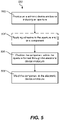
- the invention includes a method for securing a component within an electronic device enclosure.
- the method includes providing an electronic device enclosure.
- the electronic device enclosure includes at least one aperture.
- the method includes positioning a component within the at least one aperture formed through the enclosure, and welding the component to the enclosure.
- the component includes a transparent material.
- the following disclosure relates generally to electronic devices, and more particularly, to transparent materials included in electronic devices and methods for securing transparent materials in electronic devices.
- the apparatuses and electronic devices typically include two components: a first component (an enclosure) having an aperture; and a second component which includes the transparent material.
- the second component is positioned within the aperture of the first component and is laser welded directly to the first component.
- a laser is positioned above the first and second component and emits a beam through the second component, including the transparent material, to the first component to form a laser weld between the respective components.
- the need for an adhesive to bind the components may be unnecessary, and a substantially permanent coupling may be formed between the components.
- the weld may be substantially hidden from the user of the electronic device. That is, by laser welding the respective components, the weld may be substantially undetectable by, or concealed from, the user of the electronic device. Not only may the laser weld improve the coupling strength between the first and second component, but it may also improve the cosmetic features of the electronic device.
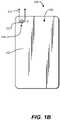
- FIGs. 1A and 1B show an illustrative front and back view, respectively, of an electronic device 100, according to embodiments.
- electronic device 100 is implemented as a mobile phone.
- Electronic device 100 may include, or may be connected to a biometric sensing device (not shown).
- Other embodiments can implement the electronic device 100 differently, such as, for example, as a laptop or desktop computer, a tablet computing device, a gaming device, a display, a digital music player, a wearable computing device or display such as a watch or glasses, and other types of electronic devices that can receive biometric data from a biometric sensing device.
- Electronic device 100 includes an enclosure 102 at least partially surrounding a display 104 and one or more buttons 106 or input devices.
- the enclosure 102 comprises an exterior surface 120 and an interior surface 126 opposite the exterior surface 120 and an angled side wall 130 extending between the exterior and interior surfaces, and defining an aperture 124.
- the enclosure 102 may form ar outer surface or partial outer surface and protective case for the internal components of the electronic device 100, and may at least partially surround the display 104.
- the enclosure 102 may be formed of one or more components operably connected together, such as a front piece and a back piece.
- enclosure 102 may include a trim piece that may be coupled to additional components configured to be operably connected to form a protective case for electronic device 100, as discussed herein.
- the enclosure 102 may be formed of a single piece operably connected to the display 104.
- Enclosure 102 may include a plurality of distinct materials including, but not limited to: corundum, commonly referred to as sapphire, metal, glass or plastic.
- enclosure 102 may include a decorative and/or coating layer that be disposed on the outer and/or or inner surface of enclosure 102. The decorative layer and/or coating layer may be disposed on the surface(s) of enclosure 102 to protect the enclosure and/or provide a decorative feature (e.g., exterior color) for electronic device 100.
- Display 104 may be implemented with any suitable technology, including, but not limited to, a multi-touch sensing touchscreen that uses liquid crystal display (LCD) technology, light emitting diode (LED) technology, organic light-emitting display (OLED) technology, organic electroluminescence (OEL) technology, or another type of display technology.
- Display 104 may include a substantially transparent layer 108 positioned above the touchscreen. That is, and as discussed herein, transparent layer 108 may be positioned above the touchscreen of display 104. The transparent layer 108 is positioned within an aperture of enclosure 102, such that enclosure 102 and transparent layer 108 are in planar alignment with front surface 112 of electronic device 100.
- Transparent layer 108 may protect display 104 from contaminents, without obstructing a user's view and/or ability to interact with display 104 and/or electronic device 100.
- Transparent layer 108 may be formed from a variety of substantially transparent materials including, but not limited to: sapphire, glass or plastic.
- Button 106 may include any conventional input/output (I/O) device for electronic device 100.
- button 106 may include an actuation component (see, FIG. 4 ) in electronic and/or mechanical communication with the internal components of electronic device 100, to provide user input and/or allow the user to interact with the various functions of electronic device 100.
- button 106 may be configured as a single component surrounded by enclosure 102.
- button 106 may include a plurality of components, including an actuation component, in mechanical/electrical communication with one another and/or internal component of electronic device 100.
- Button 106 may be formed from a transparent material, similar to transparent layer 108. That is, at least a portion of button 106 may be formed from a substantially transparent material including, but not limited to: sapphire, glass or plastic.
- electronic device 100 may also include a plurality of camera systems. More specifically, electronic device 100 may include a first camera system 110 positioned on the front surface 112 of electronic device 100 (see, FIG. 1A ) and a second camera system 118 positioned on the back surface 120 of electronic device 100 (see, FIG. 1B ). Similar to display 104 of electronic device 100, first camera system 110 and second camera system 118 may include a transparent layer positioned within enclosure 102. According to the invention, the electronic device 100 comprises a transparent window 122 positioned within the aperture 124. In a non-limiting example as shown in FIG.
- second camera system 118 may include a window 122 that may be positioned in front of the internal components of second camera system 118 and may be positioned within enclosure 102. As discussed herein, window 122 of second camera system 118 may be positioned within an aperture of enclosure 102, such that enclosure 102 and window 122 are in planar alignment with back surface 120 of electronic device 100. Also similar to transparent layer 108 of display 104, window 122 may be formed from a plurality of substantially transparent materials including, but not limited to: sapphire, glass, or plastic. Window 122 is configured to provide a transparent protective layer for second camera system 118 that may protect second camera system 118 from contaminants, without obstructing electronic device's 100 ability to take images and/or videos using second camera system 118.
- FIG. 2A shows an exploded, simplified cross-section view of a portion of electronic device 100 along line 2-2 in FIG. 1B . More specifically, FIG. 2A shows an exploded, simplified cross-section view of enclosure 102 and second camera system 118 including window 122 of electronic device 100.
- Enclosure 102 of electronic device 100 may include a plurality of distinct apertures formed therein or therethrough. Each of the plurality of apertures may be configured to receive a distinct component (e.g., window 122, transparent layer 108 of display 104, button 106) of electronic device 100.
- aperture 124 formed through enclosure 102 is configured to receive window 122 of second camera system 118.
- Aperture 124 is formed through the body of enclosure 102 and forms a passageway between an exposed or exterior surface (e.g., back surface 120) and an interior surface 126 of enclosure 102.
- the exterior surface includes back surface 120 of electronic device 100
- interior surface 126 may include a surface positioned within enclosure 102 and/or between back surface 120 and front surface 112 (see, FIG. 1A ) of electronic device 100.
- Interior surface 126 may be positioned adjacent an internal cavity 128 of electronic device 100, which may house the internal components of electronic device 100.
- the plurality of apertures (e.g., aperture 124) of enclosure 102 may be configured to receive a component or components (such as, window 122, transparent layer 108 of display 104, button 106) of electronic device 100 by having a complementary shape of the component, which includes any shape configured to accept and/or retain such a component. As discussed herein, by including complementary shapes, the component of electronic device 100 positioned within the aperture of enclosure 102 may also be adequately coupled (e.g., welded) to enclosure 102 of electronic device 100.
- aperture 124 of enclosure 102 includes angled sidewalls 130 that are complementary to the sidewalls 132 of window 122. More specifically, sidewalls 130 of aperture 124 in enclosure 102 include an angle substantially equal to the angle of sidewalls 132 of window 122 of second camera system 118. By having sidewalls that complement the angle and shape of the sidewalls, the window 122 is positioned within aperture 124 of enclosure 102, and sidewalls 130 of aperture 124 and sidewalls 132 of window 122 substantially contact one another.
- Second camera system 118 may include internal camera components 134 positioned adjacent window 122.
- Internal camera components 134 may be positioned within internal cavity 128 of electronic device 100, adjacent interior surface 126 of enclosure 102.
- internal camera components 134 may include any conventional component(s) used in second camera system 118, including a lens, a magnifier, a shutter, diaphragm, etc. Additional explanation of these components is omitted herein for clarity.
- Window 122 of second camera system 118 may include a first surface 136 and a second surface 138 positioned opposite first surface 136.
- first surface 136 may be an external surface and may be substantially exposed to the exterior of electronic device 100 and/or may be in planar alignment with the exterior surface or back surface 120 of electronic device 100.
- second surface 138 may include an internal surface positioned adjacent interior surface 126 of enclosure 102 and/or may be positioned within cavity 128 of electronic device 100.
- First surface 136 and second surface 138 of window 122 may include surface treatments. More specifically, prior to, or subsequent to, positioning window 122 within enclosure 102, first surface 136 and second surface 138 may undergo surface treatment processes including, but not limited to: lapping, planing, grinding, or polishing. In one example, first surface 136 and second surface 138 are polished prior to positioning window 122 within enclosure 102 to substantially ensure that window 122 includes an acceptable transparency that will not obstruct second camera system 118. The surface treatment processes may be performed on window 122 prior to and/or subsequent to the forming (e.g., cutting, shaping) of window 122.
- the surface treatment processes may be performed on window 122 prior to and/or subsequent to the forming (e.g., cutting, shaping) of window 122.
- sidewalls 132 of window 122 is positioned between treated first surface 136 and treated second surface 138, and is substantially angled, as discussed herein. Unlike treated first surface 136 and treated second surface 138, sidewalls 132 of window 122 is not treated. That is, sidewalls 132 of window 122 do not undergo surface treatment processes prior to window 122 being positioned within aperture 124 of enclosure 102.
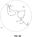
- FIG. 2B shows an enlarged portion of sidewalls 132 of window 122 as depicted in FIG. 2A .
- defects 140 are formed on the surface of sidewalls 132 of window 122 as a result of the forming processes (e.g., cutting, shaping) utilized when forming window 122.
- window 122 may be formed from a transparent, sapphire material. More specifically, window 122 may be formed by cutting window 122 from a large sheet of sapphire material.
- the cutting process used to form window 122 may create defects 140 on one or more of the various surfaces (e.g., sidewalls 132, first surface 136, second surface 138) of the sapphire.
- Surface treatment processes performed on first surface 136 and second surface 138 remove these defects 140 formed on the respective surfaces.
- untreated sidewalls 132 of window 122 maintain defects 140 when positioned within aperture 124 of enclosure 102.
- defects 140 of sidewalls 132 include a plurality of cracks 142 and/or depressions 144. As discussed herein, defects 140 may not negatively affect the coupling between window 122 and enclosure 102.
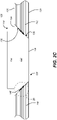
- FIG. 2C shows a cross-section view of window 122 of second camera system 118 positioned within aperture 124 of enclosure 102.
- aperture 124 of enclosure 102 includes a complementary shape (e.g., angled sidewalls 130) for receiving window 122.
- Window 122 is positioned within aperture 124 such that treated first surface 136 or external surface of window 122 may be in planar alignment with exterior surface or back surface 120 of enclosure 102. That is, as shown in FIG. 2C , the exposed surfaces (e.g., treated first surface 136, back surface 120) of window 122 and enclosure 102 may be in planar alignment, such that treated first surface 136 of window 122 and back surface 120 of enclosure 102 form a continuous, smooth surface.
- the exposed surfaces e.g., treated first surface 136, back surface 120
- Window 122 is coupled to enclosure 102. More specifically, as shown in FIG. 2C , window 122 is welded to enclosure 102 and is substantially fixed within aperture 124 of enclosure 102. As discussed herein, and as shown in FIG. 2C , enclosure 102 may include a protective casing for electronic device 100, where window 122 is welded to enclosure 102 forming the protective casing. In another non-limiting example, and as discussed herein, where enclosure 102 includes a plurality of components, and specifically where enclosure 102 includes a trim piece, window 122 may be welded to the trim piece forming enclosure 102.
- a weld interface 146 is present between sidewalls 130 of enclosure 102 and encircles the untreated sidewalls 132 of window 122 to couple the components of electronic device 100. As shown in FIG. 2C , weld interface 146 is positioned between treated first surface 136 or external surface of window 122, and treated second surface 138 or internal surface of window 122. Additionally, weld interface 146 may be positioned between exterior surface or back surface 120 and interior surface 126 of enclosure 102. As shown in FIG. 2C , weld interface 146 may be formed around an entire perimeter of sidewalls 130 of aperture 124 and/or untreated sidewalls 132 of window 122 to ensure window 122 is substantially coupled or fixed to enclosure 102.
- Weld interface 146 may include a solidified molten pool or deposit of material forming enclosure 102, that may couple or weld enclosure 102 to window 122. As discussed herein, a portion of sidewall 130 of enclosure 102 is exposed to a laser beam, which may create molten pool of a portion of material forming sidewalls 130 to weld enclosure 102 to window 122.
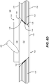
- FIG. 2D shows an enlarged portion of weld interface 146 as depicted in FIG. 2C .
- weld interface 146 is formed between sidewalls 130 of enclosure 102 and untreated sidewalls 132 of window 122 from a solidified molten pool of material forming enclosure 102.
- weld interface 146 is formed within defects 140 of untreated sidewalls 132 of window 122. More specifically, as shown in FIG. 2D , weld interface 146 is formed within cracks 142 and/or depressions 144 previously formed within untreated sidewalls 132 of window 122 when forming (e.g., cutting) window 122.
- weld interface 146 may completely contact the entire surface of sidewall 130 to affix window 122 to enclosure 102. Additionally, potential issues with defects 140 may be substantially minimized when forming weld interface 146 within defects 140 of untreated sidewall 132 of window 122.
- depression 144 formed in untreated sidewalls 132 of window 122 may substantially increase the chance of window 122 being split during an undesirable impact event (e.g., dropping electronic device 100).
- weld interface 146 fills depression 144 formed in untreated sidewalls 132 of window 122, and may provide additional structure support to window 122 and/or may provide a binding-effect within depression 144 to prevent further defect within window 122.
- weld interface 146 may not be visible to a user of electronic device 100. More specifically, because the respective angled sidewalls for window 122 and enclosure 102 extend toward internal cavity 128 and/or enclosure 102, a user of electronic device 100 viewing back surface 120 may not be able to see weld interface 146. As such, a "hidden weld" may be formed to couple window 122 to enclosure 102 of electronic device 100.
- FIG. 3 shows a front cross-section view of a portion of electronic device 100 along line 3-3 in FIG. 1A . More specifically, FIG. 3 shows a front cross-section view of transparent layer 108 of display 104 positioned within enclosure 102 in electronic device 100. It is understood that similarly named and/or numbered components may function in a substantially similar fashion. Redundant explanation of these components has been omitted for clarity.
- Transparent layer 108 of electronic device 100 includes first surface 336, which may be exposed to a user. More specifically, as shown in FIG. 3 , transparent layer 108 is positioned within enclosure 102, such that first surface 336 of transparent layer 108 is an external surface, and may be substantially exposed to the exterior of electronic device 100 and/or may be in planar alignment with the exterior surface or front surface 112 of electronic device 100. Additionally, when transparent layer 108 is positioned within aperture 324 of enclosure 102, the exposed surfaces (e.g., treated first surface 336, front surface 112) of transparent layer 108 and enclosure 102 may be in planar alignment, such that treated first surface 336 of transparent layer 108 and front surface 112 of enclosure 102 form a continuous, smooth surface.
- first surface 336 which may be exposed to a user. More specifically, as shown in FIG. 3 , transparent layer 108 is positioned within enclosure 102, such that first surface 336 of transparent layer 108 is an external surface, and may be substantially exposed to the exterior of electronic device 100 and/or may be in plan
- display 104 which may include a touchscreen, may be positioned on or adjacent to second surface 338 or internal surface of transparent layer 108 of electronic device 100. Additionally, display 104 may be positioned within internal cavity 128 and/or adjacent to interior surface 126 of enclosure 102. As discussed herein transparent layer 108 may be configured as a protective layer for display 104.
- first surface 336 and second surface 338 of transparent layer 108 include a surface treatment. That is, first surface 336 and second surface 338 of transparent layer 108 undergoes surface treatment(s) prior to transparent layer 108 being positioned within aperture 324 of enclosure 102.
- sidewalls 332 of transparent layer 108 include untreated sidewalls 332.
- untreated sidewalls 332 of transparent layer 108 may include defects 140 as a result of forming (e.g., cutting) transparent layer 108 of electronic device 100.
- transparent layer 108 of electronic device 100 is coupled or welded to enclosure 102. More specifically, transparent layer 108 is affixed within aperture 324 of enclosure 102 via weld interface 146 present between sidewalls 130 of enclosure 102 and untreated sidewalls 332 of transparent layer 108. As shown in FIG. 3 , and similarly discussed herein, weld interface 146 may be positioned between external or treated first surface 336 and internal or treated second surface 138 of transparent layer 108 and, exterior or front surface 112 and interior surface 126 of enclosure 102.
- weld interface 146 may be formed around an entire perimeter of sidewalls 130 of aperture 324 and/or untreated sidewalls 332 of transparent layer 108 to ensure transparent layer 108 is substantially coupled or welded to enclosure 102. As discussed herein, weld interface 146 may include a solidified molten pool of material forming enclosure 102, that may couple or weld transparent layer 108 to enclosure 102.
- an adhesive 348 may be positioned in aperture 324 formed through enclosure 102 and transparent layer 108. That is, adhesive 348 may be positioned between sidewalls 130 of enclosure 102 and untreated sidewalls 332 of transparent layer 108, and may be positioned adjacent weld interface 146. Adhesive 348, as shown in FIG. 3 may also be positioned between external or treated first surface 336 and internal or treated second surface 138 of transparent layer 108, and exterior or front surface 112 and interior surface 126 of enclosure 102. In a non-limiting example, adhesive 348 may be positioned between weld interface 146 and external or treated first surface 336 of transparent layer 108 and/or exterior or front surface 112 of enclosure 102.
- Adhesive 348 may be formed between weld interface 146 and the external surfaces of transparent layer 108 and/or enclosure 102 for functional and/or cosmetic purposes.
- adhesive 348 may be formed between enclosure 102 and transparent layer 108 to adhere and/or aid in the coupling of transparent layer 108 to enclosure 102.
- adhesive 348 may be formed between enclosure 102 and transparent layer 108 to hide weld interface 146. That is, adhesive 348 may be provided in electronic device 100 (see, FIG.
- Adhesive 348 formed in aperture 324 of enclosure 102 may be any conventional adhesive material capable of adhering transparent layer 108 to enclosure 102.
- adhesive 348 of FIG. 3 may be utilized with any component of electronic device 100 positioned in, and welded to, enclosure 102. That is, adhesive 348 may be utilized with window 122, as discussed herein with respect to FIGs. 2A-2D , and button 106, as discussed herein with respect to FIG. 4 .
- FIG. 4 shows a front cross-section view of a portion of electronic device 100 along line 4-4 in FIG. 1A . More specifically, FIG. 4 shows a front cross-section view of button 106 positioned within enclosure 102 in electronic device 100.
- Button 106 may include a button housing 452 made from a substantially transparent material (e.g., sapphire, glass, plastic), and an actuation component 450 positioned within button housing 452 of button 106.
- Actuation component 450 may be configured to move within button housing 452 in a direction (D), while button housing 452 remains substantially stationary and/or welded to enclosure 102, as discussed herein. Additionally, actuation component 450 of button 106 may be in mechanical and/or electronic communication with an internal button component 454 of electronic device 100.
- internal button component 454 may include a piezoelectric sensor that may be in electro-mechanical communication with actuation component 450.
- actuation component 450 of button 106 When actuation component 450 of button 106 is actuated by a user, actuation component 450 contacts and/or deforms the piezoelectric sensor to send an electronic signal to distinct, internal components of electronic device 100.
- enclosure 102 may include a bezel portion 456. More specifically, sidewalls 130 of enclosure 102 may include bezel portion 456, which may complement a protrusion portion 458 of button housing 452 of button 106. When button 106 includes protrusion portion 458, and enclosure 102 includes complementary bezel portion 456, weld interface 146 may be formed on and/or between protrusion portion 458 and bezel portion 456 to weld button 106 to enclosure 102. More specifically, as shown in FIG.
- weld interface 146 may be formed between a portion of sidewalls 130 of bezel portion 456 of enclosure 102 and a portion of untreated sidewalls 432 of protrusion portion 458 of button 106 to weld button housing 452 of button 106 to enclosure 102.
- Weld interface 146 may be positioned between external or treated first surface 436 and internal or treated second surface 438 of button 106 and, exterior or front surface 112 and interior surface 126 of enclosure 102. Additionally, weld interface 146 may be formed around an entire perimeter of bezel portion 456 of enclosure 102 and/or protrusion portion 458 of button housing 452 to ensure button 106 is substantially coupled or welded to enclosure 102.
- weld interface 146 may not be visible, or may be "hidden” from a user viewing front surface 112 of electronic device 100. More specifically, bezel portion 456 of enclosure 102 may be positioned on top of and/or may extend over protrusion portion 458 of button housing 452, such that protrusion portion 458 is not visible from front surface 112 of electronic device 100. As a result, weld interface 146 may also be covered and/or not visible from front surface 112 because of bezel portion 456.
- FIG. 5 is a flowchart depicting one sample method 500 for securing a component within an electronic device enclosure, as discussed herein with respect to FIGs. 1A-4 .
- an electronic device enclosure including at least one aperture is provided. More specifically, at least one aperture is formed through an enclosure of an electronic device to allow components of the electronic device to be viewable by a user and/or protected from contaminants.
- an adhesive may be applied to at least one of the at least one aperture formed through the electronic device enclosure, and/or a component configured to be positioned within the aperture. That is, an adhesive may be applied to a portion of the sidewalls of the apertures formed through the electronic device enclosure. Additionally, an adhesive may be applied to a portion of the component that may contact the sidewalls of the apertures when the component is positioned within the aperture. As discussed herein, the adhesive may be applied to the aperture and/or the component to adhere the component to the enclosure and/or hide a weld formed between the electronic device enclosure and the component.
- the component is positioned within the aperture formed through the electronic device enclosure. More specifically, a component of the electronic device, formed from a transparent material, is positioned within and/or received by the aperture of the electronic device enclosure.
- the aperture of the enclosure includes a complementary shape to the shape of the component. That is, the sidewalls of the aperture of the enclosure are complementary to the sidewalls of the component positioned within the enclosure.
- the component positioned within the aperture of the enclosure may include a window for a camera system (see, FIGs. 2A-2D ), a transparent layer for a display (see, FIG. 3 ), or a button (see, FIG. 4 ).
- the component positioned within the aperture of the electronic device enclosure may include additional processes prior to, or subsequent to, the positioning in operation 506. More specifically, the external surface of the component may be treated, and the internal surface of the component positioned opposite the external surface may be treated. The external surface and internal surface undergo surface treatments, such as, lapping, planing, grinding, or polishing. Additionally, prior to, subsequent to, and/or during the positioning in operation 506, untreated sidewalls of the component are substantially maintained. More specifically, the sidewalls of the component remain substantially untreated, and do not undergo surface treatments, such that the sidewalls contain defects (e.g., cracks, depressions) formed during initially processes for creating the component.
- defects e.g., cracks, depressions
- the positioning in operation 506 may also include aligning the treated external surface of the component with an exterior surface of the electronic device enclosure. More specifically, when positioning the component within the aperture, the treated external surface of the component may be in planar alignment with an exterior surface of the enclosure. By aligning the external surface of the component and the exterior surface of the enclosure, the surface of the electronic device including the component and/or the aperture may be substantially continuous and planar.
- the component is welded to the electronic device enclosure. More specifically, a laser beam is projected through the component including the transparent material, and a portion of the sidewall of the aperture formed through the enclosure is exposed to the projected laser beam.
- the laser beam wavelength may be dependent on the material composition of the component, such that material of the component is transparent to the laser beam.
- the material of the component has a melting point greater than the melting point of the material forming the enclosure.
- the exposed portion of the sidewall includes a solidified molten pool that welds the sidewall of the component to the sidewall of the aperture of the enclosure.
- the welding may also include laser welding an entire perimeter of the component to the at least one aperture formed through the enclosure. By welding the perimeter of the component, it may substantially ensure that the component is fixed to the enclosure.
- FIGs. 6A-6D a sample portion of an electronic device 100 ( see, FIG. 1A and 1B ) including an enclosure 102 and a window 122, is shown undergoing various operations of method 500 of FIG. 5 . It is understood that similarly numbered components may function in a substantially similar fashion. Redundant explanation of these components has been omitted for clarity.
- enclosure 102 of electronic device 100 (see, FIG. 1A and 1B ) is provided and includes an aperture 124, as discussed herein.
- the provided enclosure 102 including the aperture 124, as shown in FIG. 6A may correspond to operation 502 of FIG. 5 .
- Aperture 124 of enclosure 102 includes angled sidewalls 130, which complement or correspond to untreated sidewalls 132 of window 122, as discussed herein.
- window 122 is positioned within aperture 124 of enclosure 102, as discussed herein. More specifically, untreated sidewalls 132 of window 122 contact sidewalls 130 of enclosure 102, and treated external or first surface 136 may be in planar alignment with exterior or back surface 120 of enclosure 102. Window 122 positioned within aperture 124 of enclosure 102, as shown in FIG. 6A , may correspond to operation 506 of FIG. 5 .
- an adhesive may also be applied to the aperture formed through enclosure 102 prior to the positioning of window 122 within aperture 124 of enclosure 102. More specifically, an adhesive 348 ( see, FIG. 4 ) may be applied to sidewall 130 of aperture 124 to aid in adhering window 122 to enclosure 102 and/or hide a weld formed between enclosure 102 and window 122, as discussed herein. The applying of an adhesive to the aperture, if shown in FIG. 6A , would correspond to operation 504 in FIG. 5 .
- FIGs. 6B-6D window 122 is welded to enclosure 102, as discussed herein. Specifically, FIGs. 6B-6D show the progression of the laser welding process for welding window 122 to aperture 124 of enclosure 102.
- Window 122 welded to enclosure 102 corresponds to operation 508 in FIG. 5 .
- the welding process may begin on a first side of aperture 124.
- Laser 660 projects a laser beam 662 through window 122, which includes a transparent material, to expose a portion of sidewall 130 of aperture 124 formed through enclosure 102.
- laser 660 may include a predetermined wavelength that may be dependent on the transparency properties of the material forming window 122, such that window 122 is substantially transparent to laser beam 662 of laser 660. Additionally, and as discussed herein, the material forming window 122 includes a melting point higher than the material forming enclosure 102. As a result, window 122 may be substantially unaffected when laser beam 662 is projected through window 122 and a portion of sidewall 130 of enclosure 102 is exposed to laser beam 662, during the welding process.
- laser 660 may include an infrared laser, which may produce laser beam 662 having a 1064 nm wavelength, and 150W average power.
- Laser 660 may be a pulsed laser capable of pulsing laser beam 662 in micro-second pulse widths. Because sapphire's melting point (e.g., approximately 2000°C) is greater than aluminum's melting point (e.g., approximately, 1220°C), laser beam 662 pulsing through window 122 may form a molten pool of the aluminum on sidewall 130, which may ultimately create weld interface 146 ( see, FIG. 6C ), without disrupting the sapphire forming window 122.
- sapphire's melting point e.g., approximately 2000°C
- aluminum's melting point e.g., approximately, 1220°C
- laser 660 may be a continuous wave laser. Distinct from the pulsed laser, continuous wave laser may provide a continuous laser beam 662 through window 122, which includes a transparent material, to expose a portion of sidewall 130 of aperture 124 formed through enclosure 102, as discussed herein.
- Window 122 may be substantially circular in shape ( see, FIG. 1B ). As such, and as shown in FIGs. 6B and 6C , laser 660 may rotate in direction (R) to perform a circumferential weld of window 122 and enclosure 102. The circumferential weld performed by laser 660 may provide a complete perimeter weld of window 122 to ensure window 122 is fixed to enclosure 102, as discussed herein. During the circumferential welding process, as depicted in FIGs. 6B and 6C , the exposed portion of sidewall 130 of enclosure 102 may form a molten pool that may subsequently solidify, to form weld interface 146. Specifically, when comparing FIGs.
- the portion of sidewall 130 that is exposed to laser beam 662 in FIG. 6B may be solidified to form weld interface 146 by the time laser beam 662 is projected on a portion of sidewall 130 positioned opposite weld interface 146, as shown in FIG. 6C .
- window 122 may be completely welded to enclosure 102. More specifically, laser 660 may weld the entire perimeter of window 122 and may be positioned back in alignment with the portion of sidewall 130 initially exposed to laser beam 662, as shown in FIG. 6B . As a result of welding the entire perimeter of window 122, laser 660 may no longer expose sidewalls 130 of aperture 124 formed through enclosure 102 with laser beam 662. Additionally, as shown in FIG. 6D , weld interface 146 may be formed completely around window 122, for welding and/or fixing window 122 to enclosure 122.
- the material forming window 122 has a melting point higher than the material forming the enclosure 102.
- window 122 may also include a melting point equal to or less than the melting point of the material forming the enclosure 102. That is, in non-limiting examples, the material forming window 122 may include a melting point equal to, or less than the material forming enclosure 102. In these examples, window 122 may remain substantially unaffected when laser beam 662 is projected through window 122, as discussed herein, or may be minimally altered by laser beam 662.
- window 122 when window 122 is exposed to laser beam 662, window 122 may be substantially unaffected by laser beam 662, as discussed herein, or laser beam 662 may cause a minimal, surface alteration to window 122.
- the material forming window 122 may include a melting point equal to, or less than the material forming enclosure 102, window 122 may remain substantially unaffected or minimally affected as a result of laser beam 662 including a wavelength that provides window 122 to be substantially transparent to laser beam 662 of laser 660.
- window 122 includes a minimal surface alteration as a result of laser beam 662
- the minimal surface alteration may remain on second surface 138 of window 122 undetectable and/or unseen by a user or, may be removed by performing additional surface treatment processes (e.g., buffing, polishing) on second surface 138 of window 122.
- the need for an adhesive to bind the components is unnecessary.
- the need for decorative ink to hide the coupling technique e.g., the weld
- a substantially permanent coupling may be formed between the components and the enclosure.
- the weld may be substantially hidden from the user of the electronic device.
- the weld may be substantial undetectable by, or concealed from, the user of the electronic device. Not only will the laser weld improve the coupling strength between the first and second component, but it may also improve the cosmetic features of the electronic device.
Landscapes
- Physics & Mathematics (AREA)
- Engineering & Computer Science (AREA)
- Optics & Photonics (AREA)
- Mechanical Engineering (AREA)
- Plasma & Fusion (AREA)
- Health & Medical Sciences (AREA)
- Toxicology (AREA)
- Thermal Sciences (AREA)
- Electromagnetism (AREA)
- Computer Networks & Wireless Communication (AREA)
- Signal Processing (AREA)
- Chemical & Material Sciences (AREA)
- Chemical Kinetics & Catalysis (AREA)
- General Chemical & Material Sciences (AREA)
- Oil, Petroleum & Natural Gas (AREA)
- Microelectronics & Electronic Packaging (AREA)
- Human Computer Interaction (AREA)
- Casings For Electric Apparatus (AREA)
Description
- The disclosure relates generally to electronic devices, and more particularly to transparent materials included in electronic devices and methods for securing transparent materials in electronic devices.
- Conventional electronic devices typically include a plurality of working or functional components all included within a single housing or casing. These components allow a user to interact with the electronic device. Some components of the electronic device include, for example, buttons, switches, screen displays and cameras. Each of these components may include portions that are visible or exposed on an outer surface of the electronic device, and may interact or may be in communication with portions of the component located within the electronic device. For example, the button may include a contact portion positioned on the outer surface of the electronic device, and may be in communication with internal portions that may interact with the electronic device and/or distinct components (e.g., processor) of the electronic device. In another example, a display and/or camera may include transparent windows that protect the components, but allow the components to be seen/be exposed to the exterior of the electronic device.
- The components of the electronic device that are visible or exposed on an outer surface of the electronic device are typically coupled directly to the housing or include windows coupled directly to the housing. For example, the button may include a casing portion that is directly coupled to the housing, and the camera may include a window, positioned adjacent a camera lens, coupled directly to the housing. The components of the electronic device are typically coupled to the housing using an adhesive. More specifically, an adhesive is typically dispensed between the component and the housing to couple the component to the housing of the electronic device, and/or maintain the component within the housing during the operational life of the electronic device.
- The reliance on adhesive alone to couple the components to the housing of the electronic device may cause operational issues. For example, over the operational life of the electronic device, the adhesive may wear or weaken. This may cause the component (e.g., button) or portions of the component (e.g., camera window) to become displaced or uncoupled from the housing of the electronic device. When the components become displaced or uncoupled from the housing, the electronic device may not function as intended or may not function at all.
- In addition, the reliance on adhesive alone to couple the components to the housing of the electronic device may cause manufacturing issues. That is, when using adhesive to couple the components to the housing, it is typically required that the contact surfaces be treated in order to ensure adequate contact. More specifically, the contact surfaces of the component and the portion of the housing receiving the component may be planed, polished, and/or resurfaced in order to provide substantially flat contact surfaces free of defects formed during prior processing of the component (e.g., cutting, shaping). The treatment step of the contact surfaces adds time to the process of manufacturing the electronic device, especially, when the contact surfaces need to be treated multiple times and/or undergo multiple treatment processes.
- These defects may be reduced, or eliminated, by providing additional cutting or shaping processes during the manufacturing of the components. However, these additional cutting or shaping processes tend to add time to the overall manufacturing process and, dependent on the material of the component, can increase cost as well. For example, where the component is made from corundum, commonly referred to as sapphire, additional cutting processes can be performed on the component to minimize the defects on the contact surface. However, because of sapphire's hardness (e.g., 9.0 Mohs hardness scale), cutting the material can be difficult, time consuming and can result in rapid wear to the cutting tool. This rapid wear to the cutting tool may result in constant replacement and/or sharpening of the cutting tool during the manufacturing process.
- The inclusion of adhesive to couple to the components to the housing of the electronic device may increase the cost of manufacturing based on the amount of adhesive used and/or the number of components that utilize adhesive within the electronic device. That is, the adhesive itself adds an additional component to the electronic device, which also increases the cost to manufacture the electronic device, and increases the manufacture time by the amount of time it takes to apply the adhesive to the component and/or the housing of the electronic device.
- Additionally, the inclusion of adhesive to couple the components to the housing of the electronic device may require further processes in order to meet cosmetic requirements for the electronic device. For example, after adhesive is applied to couple components of the electronic device, a decorative ink may be applied to the electronic device to hide the adhesive between the components. That is, a decorative ink may be applied to a surface and/or component of the electronic device to substantially hide the adhesive, which may not be aesthetically or visually appealing. Similar to the adhesive above, the application of the decorative ink on an electronic device may increase the manufacturing time of the electronic device as well as increase the cost of manufacturing the electronic device.
-
WO 2006/048500 A1 discloses a laser welding method for welding together two plastic components. -
JP 2003/320585 A1 - "Laserstrahlschweissen von Thermoplasten im Durchstrahlverfahren", (20000201), pages 1 - 8, TECHNISCHE INFORMATION FUER EXPERTEN, XP002312668, discloses a method of laser beam welding of thermoplastics.
-
EP 1270183 A1 (basis for the preamble of claims 1 and 9) discloses a method for manufacturing an equipment housing, comprising: locating together a first housing part and a second housing part. - The invention refers to apparatuses including transparent materials, transparent materials used in electronic devices and methods for securing transparent materials in electronic devices. The apparatuses and electronic devices include two components: a first component ( enclosure) having an aperture, and a second component which includes the transparent material. The second component is positioned within the aperture of the first component and is laser welded directly to the first component. More specifically, a laser is positioned above the first and second component and emits a beam through the second component, including the transparent material, to the first component to form a laser weld between the respective components. By welding the first component to the second component, the need for an adhesive to bind the components is unnecessary, and a substantially permanent coupling may be formed between the components. Additionally, in some embodiments, by forming the laser weld between the first and second component by emitting a laser beam through the second component, the weld may be substantially hidden from the user of the electronic device. That is, by laser welding the respective components, the weld may be substantially undetectable by, or concealed from, the user of the electronic device. Not only will the laser weld improve the coupling strength between the first and second component, but it may also improve the cosmetic features of the electronic device.
- The invention includes an apparatus. The apparatus includes a first component including an aperture, and a second component including a transparent material. The second component is positioned within the aperture of the first component. The second component is welded to the first component.
- Another embodiment includes an electronic device. The electronic device includes an enclosure. The enclosure of the electronic device includes at least one aperture formed through a portion of the enclosure. Additionally, the electronic device includes a component positioned within the at least one aperture formed through the portion of the enclosure. The component is laser welded to the at least one aperture formed through the portion of the enclosure. Furthermore, the component includes a transparent material.
- The invention includes a method for securing a component within an electronic device enclosure. The method includes providing an electronic device enclosure. The electronic device enclosure includes at least one aperture. The method includes positioning a component within the at least one aperture formed through the enclosure, and welding the component to the enclosure. The component includes a transparent material.
- The disclosure will be readily understood by the following detailed description in conjunction with the accompanying drawings, wherein like reference numerals designate like structural elements, and in which:
-
FIG. 1A shows an illustrative front view of an electronic device, according to embodiments. -
FIG. 1B shows an illustrative back view of the electronic device ofFIG. 1A , according to embodiments. -
FIG. 2A shows an exploded, front cross-section view of a portion of the electronic device ofFIG. 1B taken along line 2-2 ofFIG. 1B , according to embodiments. -
FIG. 2B shows an enlarged portion of a window of the electronic device as depicted inFIG. 2A , according to embodiments. -
FIG. 2C shows a front cross-section view of a portion of the electronic device ofFIG. 1B taken along line 2-2, according to embodiments. -
FIG. 2D shows an enlarged portion of a window and enclosure of the electronic device as depicted inFIG. 2D , according to embodiments. -
FIG. 3 shows a front cross-section view of a portion of the electronic device ofFIG. 1A taken along line 3-3 ofFIG. 1A , according to embodiments. -
FIG. 4 shows a front cross-section view of a portion of the electronic device ofFIG. 1A taken along line 4-4 ofFIG. 1A , according to embodiments. -
FIG. 5 shows a flow chart illustrating a method for securing a component within an electronic device enclosure. -
FIGS. 6A-6D show illustrative views of a portion of an electronic device, including a window and an enclosure, undergoing processes of securing as depicted inFIG. 5 , according to embodiments. - It is noted that the drawings of the invention are not necessarily to scale. The drawings are intended to depict only typical aspects of the invention, and therefore should not be considered as limiting the scope of the invention. In the drawings, like numbering represents like elements between the drawings.
- Reference will now be made in detail to representative embodiments illustrated in the accompanying drawings. It should be understood that the following descriptions are not intended to limit the embodiments to one preferred embodiment. To the contrary, it is intended to cover alternatives, modifications, and equivalents as can be included within the spirit and scope of the described embodiments as defined by the appended claims.
- The following disclosure relates generally to electronic devices, and more particularly, to transparent materials included in electronic devices and methods for securing transparent materials in electronic devices.
- Discussed herein are apparatuses including transparent materials, transparent materials used in electronic devices and methods for securing transparent materials in electronic devices. The apparatuses and electronic devices typically include two components: a first component (an enclosure) having an aperture; and a second component which includes the transparent material. The second component is positioned within the aperture of the first component and is laser welded directly to the first component.
- More specifically, a laser is positioned above the first and second component and emits a beam through the second component, including the transparent material, to the first component to form a laser weld between the respective components. By welding the first component to the second component, the need for an adhesive to bind the components may be unnecessary, and a substantially permanent coupling may be formed between the components. Additionally, in some embodiments, by forming the laser weld between the first and second component by emitting a laser beam through the second component, the weld may be substantially hidden from the user of the electronic device. That is, by laser welding the respective components, the weld may be substantially undetectable by, or concealed from, the user of the electronic device. Not only may the laser weld improve the coupling strength between the first and second component, but it may also improve the cosmetic features of the electronic device.
- These and other embodiments are discussed below with reference to
FIGs. 1A - 6D . However, those skilled in the art will readily appreciate that the detailed description given herein with respect to these Figures is for explanatory purposes only and should not be construed as limiting. -
FIGs. 1A and1B show an illustrative front and back view, respectively, of anelectronic device 100, according to embodiments. In the illustrated embodiment,electronic device 100 is implemented as a mobile phone.Electronic device 100 may include, or may be connected to a biometric sensing device (not shown). Other embodiments can implement theelectronic device 100 differently, such as, for example, as a laptop or desktop computer, a tablet computing device, a gaming device, a display, a digital music player, a wearable computing device or display such as a watch or glasses, and other types of electronic devices that can receive biometric data from a biometric sensing device. -
Electronic device 100 includes anenclosure 102 at least partially surrounding adisplay 104 and one ormore buttons 106 or input devices. Theenclosure 102 comprises anexterior surface 120 and aninterior surface 126 opposite theexterior surface 120 and anangled side wall 130 extending between the exterior and interior surfaces, and defining anaperture 124. Theenclosure 102 may form ar outer surface or partial outer surface and protective case for the internal components of theelectronic device 100, and may at least partially surround thedisplay 104. Theenclosure 102 may be formed of one or more components operably connected together, such as a front piece and a back piece. In a non-limiting example, whereenclosure 102 may be formed from a plurality of components,enclosure 102 may include a trim piece that may be coupled to additional components configured to be operably connected to form a protective case forelectronic device 100, as discussed herein. Alternatively, theenclosure 102 may be formed of a single piece operably connected to thedisplay 104.Enclosure 102 may include a plurality of distinct materials including, but not limited to: corundum, commonly referred to as sapphire, metal, glass or plastic. Additionally,enclosure 102 may include a decorative and/or coating layer that be disposed on the outer and/or or inner surface ofenclosure 102. The decorative layer and/or coating layer may be disposed on the surface(s) ofenclosure 102 to protect the enclosure and/or provide a decorative feature (e.g., exterior color) forelectronic device 100. -
Display 104 may be implemented with any suitable technology, including, but not limited to, a multi-touch sensing touchscreen that uses liquid crystal display (LCD) technology, light emitting diode (LED) technology, organic light-emitting display (OLED) technology, organic electroluminescence (OEL) technology, or another type of display technology.Display 104 may include a substantiallytransparent layer 108 positioned above the touchscreen. That is, and as discussed herein,transparent layer 108 may be positioned above the touchscreen ofdisplay 104. Thetransparent layer 108 is positioned within an aperture ofenclosure 102, such thatenclosure 102 andtransparent layer 108 are in planar alignment withfront surface 112 ofelectronic device 100.Transparent layer 108 may protectdisplay 104 from contaminents, without obstructing a user's view and/or ability to interact withdisplay 104 and/orelectronic device 100.Transparent layer 108 may be formed from a variety of substantially transparent materials including, but not limited to: sapphire, glass or plastic. -
Button 106 may include any conventional input/output (I/O) device forelectronic device 100. Specifically,button 106 may include an actuation component (see,FIG. 4 ) in electronic and/or mechanical communication with the internal components ofelectronic device 100, to provide user input and/or allow the user to interact with the various functions ofelectronic device 100. In anembodiment button 106 may be configured as a single component surrounded byenclosure 102. Alternatively,button 106 may include a plurality of components, including an actuation component, in mechanical/electrical communication with one another and/or internal component ofelectronic device 100.Button 106 may be formed from a transparent material, similar totransparent layer 108. That is, at least a portion ofbutton 106 may be formed from a substantially transparent material including, but not limited to: sapphire, glass or plastic. - As shown in
FIGs. 1A and1B ,electronic device 100 may also include a plurality of camera systems. More specifically,electronic device 100 may include afirst camera system 110 positioned on thefront surface 112 of electronic device 100 (see,FIG. 1A ) and asecond camera system 118 positioned on theback surface 120 of electronic device 100 (see,FIG. 1B ). Similar to display 104 ofelectronic device 100,first camera system 110 andsecond camera system 118 may include a transparent layer positioned withinenclosure 102. According to the invention, theelectronic device 100 comprises atransparent window 122 positioned within theaperture 124. In a non-limiting example as shown inFIG. 1B ,second camera system 118 may include awindow 122 that may be positioned in front of the internal components ofsecond camera system 118 and may be positioned withinenclosure 102. As discussed herein,window 122 ofsecond camera system 118 may be positioned within an aperture ofenclosure 102, such thatenclosure 102 andwindow 122 are in planar alignment withback surface 120 ofelectronic device 100. Also similar totransparent layer 108 ofdisplay 104,window 122 may be formed from a plurality of substantially transparent materials including, but not limited to: sapphire, glass, or plastic.Window 122 is configured to provide a transparent protective layer forsecond camera system 118 that may protectsecond camera system 118 from contaminants, without obstructing electronic device's 100 ability to take images and/or videos usingsecond camera system 118. -
FIG. 2A shows an exploded, simplified cross-section view of a portion ofelectronic device 100 along line 2-2 inFIG. 1B . More specifically,FIG. 2A shows an exploded, simplified cross-section view ofenclosure 102 andsecond camera system 118 includingwindow 122 ofelectronic device 100.Enclosure 102 ofelectronic device 100 may include a plurality of distinct apertures formed therein or therethrough. Each of the plurality of apertures may be configured to receive a distinct component (e.g.,window 122,transparent layer 108 ofdisplay 104, button 106) ofelectronic device 100. - As shown in
FIG. 2A , and as discussed herein,aperture 124 formed throughenclosure 102 is configured to receivewindow 122 ofsecond camera system 118.Aperture 124 is formed through the body ofenclosure 102 and forms a passageway between an exposed or exterior surface (e.g., back surface 120) and aninterior surface 126 ofenclosure 102. As shown inFIG. 2A , the exterior surface includes backsurface 120 ofelectronic device 100, andinterior surface 126 may include a surface positioned withinenclosure 102 and/or betweenback surface 120 and front surface 112 (see,FIG. 1A ) ofelectronic device 100.Interior surface 126 may be positioned adjacent aninternal cavity 128 ofelectronic device 100, which may house the internal components ofelectronic device 100. - The plurality of apertures (e.g., aperture 124) of
enclosure 102 may be configured to receive a component or components (such as,window 122,transparent layer 108 ofdisplay 104, button 106) ofelectronic device 100 by having a complementary shape of the component, which includes any shape configured to accept and/or retain such a component. As discussed herein, by including complementary shapes, the component ofelectronic device 100 positioned within the aperture ofenclosure 102 may also be adequately coupled (e.g., welded) toenclosure 102 ofelectronic device 100. - As shown in
FIGs. 2A and2B ,aperture 124 ofenclosure 102 includesangled sidewalls 130 that are complementary to thesidewalls 132 ofwindow 122. More specifically, sidewalls 130 ofaperture 124 inenclosure 102 include an angle substantially equal to the angle ofsidewalls 132 ofwindow 122 ofsecond camera system 118. By having sidewalls that complement the angle and shape of the sidewalls, thewindow 122 is positioned withinaperture 124 ofenclosure 102, and sidewalls 130 ofaperture 124 andsidewalls 132 ofwindow 122 substantially contact one another. -
Second camera system 118 may includeinternal camera components 134 positionedadjacent window 122.Internal camera components 134 may be positioned withininternal cavity 128 ofelectronic device 100, adjacentinterior surface 126 ofenclosure 102. As shown inFIG. 2A ,internal camera components 134 may include any conventional component(s) used insecond camera system 118, including a lens, a magnifier, a shutter, diaphragm, etc. Additional explanation of these components is omitted herein for clarity. -
Window 122 ofsecond camera system 118 may include afirst surface 136 and asecond surface 138 positioned oppositefirst surface 136. As discussed herein, whenwindow 122 is positioned withinenclosure 102,first surface 136 may be an external surface and may be substantially exposed to the exterior ofelectronic device 100 and/or may be in planar alignment with the exterior surface or backsurface 120 ofelectronic device 100. Furthermore, and as discussed herein, whenwindow 122 is positioned withinenclosure 102,second surface 138 may include an internal surface positioned adjacentinterior surface 126 ofenclosure 102 and/or may be positioned withincavity 128 ofelectronic device 100. -
First surface 136 andsecond surface 138 ofwindow 122 may include surface treatments. More specifically, prior to, or subsequent to,positioning window 122 withinenclosure 102,first surface 136 andsecond surface 138 may undergo surface treatment processes including, but not limited to: lapping, planing, grinding, or polishing. In one example,first surface 136 andsecond surface 138 are polished prior topositioning window 122 withinenclosure 102 to substantially ensure thatwindow 122 includes an acceptable transparency that will not obstructsecond camera system 118. The surface treatment processes may be performed onwindow 122 prior to and/or subsequent to the forming (e.g., cutting, shaping) ofwindow 122. - As shown in
FIG. 2A , sidewalls 132 ofwindow 122 is positioned between treatedfirst surface 136 and treatedsecond surface 138, and is substantially angled, as discussed herein. Unlike treatedfirst surface 136 and treatedsecond surface 138, sidewalls 132 ofwindow 122 is not treated. That is, sidewalls 132 ofwindow 122 do not undergo surface treatment processes prior towindow 122 being positioned withinaperture 124 ofenclosure 102. - As a result of not performing surface treatment processes on
sidewalls 132,untreated sidewalls 132 ofwindow 122 includedefects 140.FIG. 2B shows an enlarged portion ofsidewalls 132 ofwindow 122 as depicted inFIG. 2A . As shown inFIG. 2B ,defects 140 are formed on the surface ofsidewalls 132 ofwindow 122 as a result of the forming processes (e.g., cutting, shaping) utilized when formingwindow 122. In a non-limiting example,window 122 may be formed from a transparent, sapphire material. More specifically,window 122 may be formed by cuttingwindow 122 from a large sheet of sapphire material. Because sapphire is hard and brittle, the cutting process used to formwindow 122 may createdefects 140 on one or more of the various surfaces (e.g., sidewalls 132,first surface 136, second surface 138) of the sapphire. Surface treatment processes performed onfirst surface 136 andsecond surface 138 remove thesedefects 140 formed on the respective surfaces. However,untreated sidewalls 132 ofwindow 122 maintaindefects 140 when positioned withinaperture 124 ofenclosure 102. As shown inFIG. 2B ,defects 140 ofsidewalls 132 include a plurality ofcracks 142 and/ordepressions 144. As discussed herein,defects 140 may not negatively affect the coupling betweenwindow 122 andenclosure 102. -
FIG. 2C shows a cross-section view ofwindow 122 ofsecond camera system 118 positioned withinaperture 124 ofenclosure 102. As discussed herein,aperture 124 ofenclosure 102 includes a complementary shape (e.g., angled sidewalls 130) for receivingwindow 122.Window 122 is positioned withinaperture 124 such that treatedfirst surface 136 or external surface ofwindow 122 may be in planar alignment with exterior surface or backsurface 120 ofenclosure 102. That is, as shown inFIG. 2C , the exposed surfaces (e.g., treatedfirst surface 136, back surface 120) ofwindow 122 andenclosure 102 may be in planar alignment, such that treatedfirst surface 136 ofwindow 122 andback surface 120 ofenclosure 102 form a continuous, smooth surface. -
Window 122 is coupled toenclosure 102. More specifically, as shown inFIG. 2C ,window 122 is welded toenclosure 102 and is substantially fixed withinaperture 124 ofenclosure 102. As discussed herein, and as shown inFIG. 2C ,enclosure 102 may include a protective casing forelectronic device 100, wherewindow 122 is welded toenclosure 102 forming the protective casing. In another non-limiting example, and as discussed herein, whereenclosure 102 includes a plurality of components, and specifically whereenclosure 102 includes a trim piece,window 122 may be welded to the trimpiece forming enclosure 102. - In
coupling window 122 toenclosure 102, aweld interface 146 is present betweensidewalls 130 ofenclosure 102 and encircles theuntreated sidewalls 132 ofwindow 122 to couple the components ofelectronic device 100. As shown inFIG. 2C ,weld interface 146 is positioned between treatedfirst surface 136 or external surface ofwindow 122, and treatedsecond surface 138 or internal surface ofwindow 122. Additionally,weld interface 146 may be positioned between exterior surface or backsurface 120 andinterior surface 126 ofenclosure 102. As shown inFIG. 2C ,weld interface 146 may be formed around an entire perimeter ofsidewalls 130 ofaperture 124 and/oruntreated sidewalls 132 ofwindow 122 to ensurewindow 122 is substantially coupled or fixed toenclosure 102.Weld interface 146 may include a solidified molten pool or deposit ofmaterial forming enclosure 102, that may couple orweld enclosure 102 towindow 122. As discussed herein, a portion ofsidewall 130 ofenclosure 102 is exposed to a laser beam, which may create molten pool of a portion ofmaterial forming sidewalls 130 toweld enclosure 102 towindow 122. -
FIG. 2D shows an enlarged portion ofweld interface 146 as depicted inFIG. 2C . As discussed herein,weld interface 146 is formed betweensidewalls 130 ofenclosure 102 anduntreated sidewalls 132 ofwindow 122 from a solidified molten pool ofmaterial forming enclosure 102. As a result of the weld being formed from the solidified molten pool ofmaterial forming enclosure 102,weld interface 146 is formed withindefects 140 ofuntreated sidewalls 132 ofwindow 122. More specifically, as shown inFIG. 2D ,weld interface 146 is formed withincracks 142 and/ordepressions 144 previously formed withinuntreated sidewalls 132 ofwindow 122 when forming (e.g., cutting)window 122. By formingweld interface 146 withindefects 140 ofuntreated sidewall 132 ofwindow 122,weld interface 146 may completely contact the entire surface ofsidewall 130 to affixwindow 122 toenclosure 102. Additionally, potential issues withdefects 140 may be substantially minimized when formingweld interface 146 withindefects 140 ofuntreated sidewall 132 ofwindow 122. In a non-limiting example,depression 144 formed inuntreated sidewalls 132 ofwindow 122 may substantially increase the chance ofwindow 122 being split during an undesirable impact event (e.g., dropping electronic device 100). However,weld interface 146 fillsdepression 144 formed inuntreated sidewalls 132 ofwindow 122, and may provide additional structure support towindow 122 and/or may provide a binding-effect withindepression 144 to prevent further defect withinwindow 122. - As a result of
angled sidewalls 132 ofwindow 122 and correspondingangled sidewalls 130 ofenclosure 102,weld interface 146 may not be visible to a user ofelectronic device 100. More specifically, because the respective angled sidewalls forwindow 122 andenclosure 102 extend towardinternal cavity 128 and/orenclosure 102, a user ofelectronic device 100 viewing backsurface 120 may not be able to seeweld interface 146. As such, a "hidden weld" may be formed tocouple window 122 toenclosure 102 ofelectronic device 100. -
FIG. 3 shows a front cross-section view of a portion ofelectronic device 100 along line 3-3 inFIG. 1A . More specifically,FIG. 3 shows a front cross-section view oftransparent layer 108 ofdisplay 104 positioned withinenclosure 102 inelectronic device 100. It is understood that similarly named and/or numbered components may function in a substantially similar fashion. Redundant explanation of these components has been omitted for clarity. -
Transparent layer 108 ofelectronic device 100 includesfirst surface 336, which may be exposed to a user. More specifically, as shown inFIG. 3 ,transparent layer 108 is positioned withinenclosure 102, such thatfirst surface 336 oftransparent layer 108 is an external surface, and may be substantially exposed to the exterior ofelectronic device 100 and/or may be in planar alignment with the exterior surface orfront surface 112 ofelectronic device 100. Additionally, whentransparent layer 108 is positioned withinaperture 324 ofenclosure 102, the exposed surfaces (e.g., treatedfirst surface 336, front surface 112) oftransparent layer 108 andenclosure 102 may be in planar alignment, such that treatedfirst surface 336 oftransparent layer 108 andfront surface 112 ofenclosure 102 form a continuous, smooth surface. - As shown in
FIG. 3 ,display 104, which may include a touchscreen, may be positioned on or adjacent tosecond surface 338 or internal surface oftransparent layer 108 ofelectronic device 100. Additionally,display 104 may be positioned withininternal cavity 128 and/or adjacent tointerior surface 126 ofenclosure 102. As discussed hereintransparent layer 108 may be configured as a protective layer fordisplay 104. - As similarly discussed herein with respect to
window 122,first surface 336 andsecond surface 338 oftransparent layer 108 include a surface treatment. That is,first surface 336 andsecond surface 338 oftransparent layer 108 undergoes surface treatment(s) prior totransparent layer 108 being positioned withinaperture 324 ofenclosure 102. To the contrary of treatedfirst surface 336 and treatedsecond surface 338, but similar tosidewalls 132 ofwindow 122 inFIGs. 2A-2D , sidewalls 332 oftransparent layer 108 includeuntreated sidewalls 332. As a result,untreated sidewalls 332 oftransparent layer 108 may includedefects 140 as a result of forming (e.g., cutting)transparent layer 108 ofelectronic device 100. - Similar to
window 122 shown inFIGs. 2A-2D ,transparent layer 108 ofelectronic device 100, as shown inFIG. 3 , is coupled or welded toenclosure 102. More specifically,transparent layer 108 is affixed withinaperture 324 ofenclosure 102 viaweld interface 146 present betweensidewalls 130 ofenclosure 102 anduntreated sidewalls 332 oftransparent layer 108. As shown inFIG. 3 , and similarly discussed herein,weld interface 146 may be positioned between external or treatedfirst surface 336 and internal or treatedsecond surface 138 oftransparent layer 108 and, exterior orfront surface 112 andinterior surface 126 ofenclosure 102. Additionally,weld interface 146 may be formed around an entire perimeter ofsidewalls 130 ofaperture 324 and/oruntreated sidewalls 332 oftransparent layer 108 to ensuretransparent layer 108 is substantially coupled or welded toenclosure 102. As discussed herein,weld interface 146 may include a solidified molten pool ofmaterial forming enclosure 102, that may couple or weldtransparent layer 108 toenclosure 102. - As shown in
FIG. 3 , an adhesive 348 may be positioned inaperture 324 formed throughenclosure 102 andtransparent layer 108. That is, adhesive 348 may be positioned betweensidewalls 130 ofenclosure 102 anduntreated sidewalls 332 oftransparent layer 108, and may be positionedadjacent weld interface 146.Adhesive 348, as shown inFIG. 3 may also be positioned between external or treatedfirst surface 336 and internal or treatedsecond surface 138 oftransparent layer 108, and exterior orfront surface 112 andinterior surface 126 ofenclosure 102. In a non-limiting example, adhesive 348 may be positioned betweenweld interface 146 and external or treatedfirst surface 336 oftransparent layer 108 and/or exterior orfront surface 112 ofenclosure 102. Adhesive 348 may be formed betweenweld interface 146 and the external surfaces oftransparent layer 108 and/orenclosure 102 for functional and/or cosmetic purposes. In a non-limiting example of functionality, adhesive 348 may be formed betweenenclosure 102 andtransparent layer 108 to adhere and/or aid in the coupling oftransparent layer 108 toenclosure 102. In a non-limiting example of cosmetic application, adhesive 348 may be formed betweenenclosure 102 andtransparent layer 108 to hideweld interface 146. That is, adhesive 348 may be provided in electronic device 100 (see,FIG. 1A ) to substantially prevent a user ofelectronic device 100 from seeingweld interface 146 formed betweenenclosure 102 andtransparent layer 108, whereweld interface 146 may not be "hidden" from a user due to the configuration or shape of the components (e.g.,enclosure 102, transparent layer 108) ofelectronic device 100. Adhesive 348 formed inaperture 324 ofenclosure 102 may be any conventional adhesive material capable of adheringtransparent layer 108 toenclosure 102. - Although shown and discussed herein as being used with
transparent layer 108, it is understood thatadhesive 348 ofFIG. 3 may be utilized with any component ofelectronic device 100 positioned in, and welded to,enclosure 102. That is, adhesive 348 may be utilized withwindow 122, as discussed herein with respect toFIGs. 2A-2D , andbutton 106, as discussed herein with respect toFIG. 4 . -
FIG. 4 shows a front cross-section view of a portion ofelectronic device 100 along line 4-4 inFIG. 1A . More specifically,FIG. 4 shows a front cross-section view ofbutton 106 positioned withinenclosure 102 inelectronic device 100.Button 106 may include abutton housing 452 made from a substantially transparent material (e.g., sapphire, glass, plastic), and anactuation component 450 positioned withinbutton housing 452 ofbutton 106.Actuation component 450 may be configured to move withinbutton housing 452 in a direction (D), whilebutton housing 452 remains substantially stationary and/or welded toenclosure 102, as discussed herein. Additionally,actuation component 450 ofbutton 106 may be in mechanical and/or electronic communication with aninternal button component 454 ofelectronic device 100. In a non-limiting example,internal button component 454 may include a piezoelectric sensor that may be in electro-mechanical communication withactuation component 450. Whenactuation component 450 ofbutton 106 is actuated by a user,actuation component 450 contacts and/or deforms the piezoelectric sensor to send an electronic signal to distinct, internal components ofelectronic device 100. - As shown in
FIG. 4 ,enclosure 102 may include abezel portion 456. More specifically, sidewalls 130 ofenclosure 102 may includebezel portion 456, which may complement aprotrusion portion 458 ofbutton housing 452 ofbutton 106. Whenbutton 106 includesprotrusion portion 458, andenclosure 102 includescomplementary bezel portion 456,weld interface 146 may be formed on and/or betweenprotrusion portion 458 andbezel portion 456 toweld button 106 toenclosure 102. More specifically, as shown inFIG. 4 ,weld interface 146 may be formed between a portion ofsidewalls 130 ofbezel portion 456 ofenclosure 102 and a portion ofuntreated sidewalls 432 ofprotrusion portion 458 ofbutton 106 toweld button housing 452 ofbutton 106 toenclosure 102.Weld interface 146 may be positioned between external or treatedfirst surface 436 and internal or treatedsecond surface 438 ofbutton 106 and, exterior orfront surface 112 andinterior surface 126 ofenclosure 102. Additionally,weld interface 146 may be formed around an entire perimeter ofbezel portion 456 ofenclosure 102 and/orprotrusion portion 458 ofbutton housing 452 to ensurebutton 106 is substantially coupled or welded toenclosure 102. - By providing
weld interface 146 betweenprotrusion portion 458 ofbutton housing 452 andbezel portion 456 ofenclosure 102,weld interface 146 may not be visible, or may be "hidden" from a user viewingfront surface 112 ofelectronic device 100. More specifically,bezel portion 456 ofenclosure 102 may be positioned on top of and/or may extend overprotrusion portion 458 ofbutton housing 452, such thatprotrusion portion 458 is not visible fromfront surface 112 ofelectronic device 100. As a result,weld interface 146 may also be covered and/or not visible fromfront surface 112 because ofbezel portion 456. - Turning to
FIG. 5 , a method of securing a component within an electronic device enclosure (see,FIGs. 1A and1B ) is now discussed. Specifically,FIG. 5 is a flowchart depicting onesample method 500 for securing a component within an electronic device enclosure, as discussed herein with respect toFIGs. 1A-4 . - In
operation 502, an electronic device enclosure including at least one aperture is provided. More specifically, at least one aperture is formed through an enclosure of an electronic device to allow components of the electronic device to be viewable by a user and/or protected from contaminants. - In
optional operation 504, an adhesive may be applied to at least one of the at least one aperture formed through the electronic device enclosure, and/or a component configured to be positioned within the aperture. That is, an adhesive may be applied to a portion of the sidewalls of the apertures formed through the electronic device enclosure. Additionally, an adhesive may be applied to a portion of the component that may contact the sidewalls of the apertures when the component is positioned within the aperture. As discussed herein, the adhesive may be applied to the aperture and/or the component to adhere the component to the enclosure and/or hide a weld formed between the electronic device enclosure and the component. - In
operation 506, the component is positioned within the aperture formed through the electronic device enclosure. More specifically, a component of the electronic device, formed from a transparent material, is positioned within and/or received by the aperture of the electronic device enclosure. As discussed herein, the aperture of the enclosure includes a complementary shape to the shape of the component. That is, the sidewalls of the aperture of the enclosure are complementary to the sidewalls of the component positioned within the enclosure. In non-limiting examples, and as discussed herein, the component positioned within the aperture of the enclosure may include a window for a camera system (see,FIGs. 2A-2D ), a transparent layer for a display (see,FIG. 3 ), or a button (see,FIG. 4 ). - The component positioned within the aperture of the electronic device enclosure may include additional processes prior to, or subsequent to, the positioning in
operation 506. More specifically, the external surface of the component may be treated, and the internal surface of the component positioned opposite the external surface may be treated. The external surface and internal surface undergo surface treatments, such as, lapping, planing, grinding, or polishing. Additionally, prior to, subsequent to, and/or during the positioning inoperation 506, untreated sidewalls of the component are substantially maintained. More specifically, the sidewalls of the component remain substantially untreated, and do not undergo surface treatments, such that the sidewalls contain defects (e.g., cracks, depressions) formed during initially processes for creating the component. - The positioning in
operation 506 may also include aligning the treated external surface of the component with an exterior surface of the electronic device enclosure. More specifically, when positioning the component within the aperture, the treated external surface of the component may be in planar alignment with an exterior surface of the enclosure. By aligning the external surface of the component and the exterior surface of the enclosure, the surface of the electronic device including the component and/or the aperture may be substantially continuous and planar. - In
operation 508, the component is welded to the electronic device enclosure. More specifically, a laser beam is projected through the component including the transparent material, and a portion of the sidewall of the aperture formed through the enclosure is exposed to the projected laser beam. The laser beam wavelength may be dependent on the material composition of the component, such that material of the component is transparent to the laser beam. As a result of the laser beam being projected through the component, the material of the component has a melting point greater than the melting point of the material forming the enclosure. When the laser beam is exposed to a portion of the sidewall of the enclosure through the component, the exposed portion of the sidewall includes a solidified molten pool that welds the sidewall of the component to the sidewall of the aperture of the enclosure. The welding may also include laser welding an entire perimeter of the component to the at least one aperture formed through the enclosure. By welding the perimeter of the component, it may substantially ensure that the component is fixed to the enclosure. - Turning to
FIGs. 6A-6D , a sample portion of an electronic device 100 (see,FIG. 1A and1B ) including anenclosure 102 and awindow 122, is shown undergoing various operations ofmethod 500 ofFIG. 5 . It is understood that similarly numbered components may function in a substantially similar fashion. Redundant explanation of these components has been omitted for clarity. - As shown in
FIG. 6A ,enclosure 102 of electronic device 100 (see,FIG. 1A and1B ) is provided and includes anaperture 124, as discussed herein. The providedenclosure 102 including theaperture 124, as shown inFIG. 6A , may correspond tooperation 502 ofFIG. 5 .Aperture 124 ofenclosure 102 includesangled sidewalls 130, which complement or correspond tountreated sidewalls 132 ofwindow 122, as discussed herein. - Also shown in
FIG. 6A ,window 122 is positioned withinaperture 124 ofenclosure 102, as discussed herein. More specifically,untreated sidewalls 132 ofwindow 122 contact sidewalls 130 ofenclosure 102, and treated external orfirst surface 136 may be in planar alignment with exterior orback surface 120 ofenclosure 102.Window 122 positioned withinaperture 124 ofenclosure 102, as shown inFIG. 6A , may correspond tooperation 506 ofFIG. 5 . - Although not shown in
FIG. 6A , it is understood that an adhesive may also be applied to the aperture formed throughenclosure 102 prior to the positioning ofwindow 122 withinaperture 124 ofenclosure 102. More specifically, an adhesive 348 (see,FIG. 4 ) may be applied tosidewall 130 ofaperture 124 to aid in adheringwindow 122 toenclosure 102 and/or hide a weld formed betweenenclosure 102 andwindow 122, as discussed herein. The applying of an adhesive to the aperture, if shown inFIG. 6A , would correspond tooperation 504 inFIG. 5 . - Turning to
FIGs. 6B-6D ,window 122 is welded toenclosure 102, as discussed herein. Specifically,FIGs. 6B-6D show the progression of the laser welding process for weldingwindow 122 toaperture 124 ofenclosure 102.Window 122 welded toenclosure 102, as shown inFIGs. 6B-6D , corresponds tooperation 508 inFIG. 5 . As shown inFIG. 6B , the welding process may begin on a first side ofaperture 124.Laser 660 projects alaser beam 662 throughwindow 122, which includes a transparent material, to expose a portion ofsidewall 130 ofaperture 124 formed throughenclosure 102. As discussed herein,laser 660 may include a predetermined wavelength that may be dependent on the transparency properties of thematerial forming window 122, such thatwindow 122 is substantially transparent tolaser beam 662 oflaser 660. Additionally, and as discussed herein, thematerial forming window 122 includes a melting point higher than thematerial forming enclosure 102. As a result,window 122 may be substantially unaffected whenlaser beam 662 is projected throughwindow 122 and a portion ofsidewall 130 ofenclosure 102 is exposed tolaser beam 662, during the welding process. - In a non-limiting example, where
window 122 is formed from sapphire andenclosure 102 is formed from aluminum,laser 660 may include an infrared laser, which may producelaser beam 662 having a 1064 nm wavelength, and 150W average power.Laser 660 may be a pulsed laser capable of pulsinglaser beam 662 in micro-second pulse widths. Because sapphire's melting point (e.g., approximately 2000°C) is greater than aluminum's melting point (e.g., approximately, 1220°C),laser beam 662 pulsing throughwindow 122 may form a molten pool of the aluminum onsidewall 130, which may ultimately create weld interface 146 (see,FIG. 6C ), without disrupting thesapphire forming window 122. In an additional non-limiting example,laser 660 may be a continuous wave laser. Distinct from the pulsed laser, continuous wave laser may provide acontinuous laser beam 662 throughwindow 122, which includes a transparent material, to expose a portion ofsidewall 130 ofaperture 124 formed throughenclosure 102, as discussed herein. -
Window 122 may be substantially circular in shape (see,FIG. 1B ). As such, and as shown inFIGs. 6B and6C ,laser 660 may rotate in direction (R) to perform a circumferential weld ofwindow 122 andenclosure 102. The circumferential weld performed bylaser 660 may provide a complete perimeter weld ofwindow 122 to ensurewindow 122 is fixed toenclosure 102, as discussed herein. During the circumferential welding process, as depicted inFIGs. 6B and6C , the exposed portion ofsidewall 130 ofenclosure 102 may form a molten pool that may subsequently solidify, to formweld interface 146. Specifically, when comparingFIGs. 6B and6C , the portion ofsidewall 130 that is exposed tolaser beam 662 inFIG. 6B may be solidified to formweld interface 146 by thetime laser beam 662 is projected on a portion ofsidewall 130 positionedopposite weld interface 146, as shown inFIG. 6C . - As shown in
FIG. 6D ,window 122 may be completely welded toenclosure 102. More specifically,laser 660 may weld the entire perimeter ofwindow 122 and may be positioned back in alignment with the portion ofsidewall 130 initially exposed tolaser beam 662, as shown inFIG. 6B . As a result of welding the entire perimeter ofwindow 122,laser 660 may no longer exposesidewalls 130 ofaperture 124 formed throughenclosure 102 withlaser beam 662. Additionally, as shown inFIG. 6D ,weld interface 146 may be formed completely aroundwindow 122, for welding and/or fixingwindow 122 toenclosure 122. - In the invention the
material forming window 122 has a melting point higher than the material forming theenclosure 102. However, in other examples that do not form part of the claimed invention, it is understood thatwindow 122 may also include a melting point equal to or less than the melting point of the material forming theenclosure 102. That is, in non-limiting examples, thematerial forming window 122 may include a melting point equal to, or less than thematerial forming enclosure 102. In these examples,window 122 may remain substantially unaffected whenlaser beam 662 is projected throughwindow 122, as discussed herein, or may be minimally altered bylaser beam 662. In these non-limiting examples, whenwindow 122 is exposed tolaser beam 662,window 122 may be substantially unaffected bylaser beam 662, as discussed herein, orlaser beam 662 may cause a minimal, surface alteration towindow 122. Although thematerial forming window 122 may include a melting point equal to, or less than thematerial forming enclosure 102,window 122 may remain substantially unaffected or minimally affected as a result oflaser beam 662 including a wavelength that provideswindow 122 to be substantially transparent tolaser beam 662 oflaser 660. Wherewindow 122 includes a minimal surface alteration as a result oflaser beam 662, the minimal surface alteration may remain onsecond surface 138 ofwindow 122 undetectable and/or unseen by a user or, may be removed by performing additional surface treatment processes (e.g., buffing, polishing) onsecond surface 138 ofwindow 122. - By welding the components (e.g., window, button) of the electronic device to the enclosure of the electronic device, the need for an adhesive to bind the components is unnecessary. Also, in welding the components of the electronic device to the enclosure, the need for decorative ink to hide the coupling technique (e.g., the weld) may be unnecessary, as the weld is substantially small and/or undetectable by a user of the electronic device. Additionally, by welding the components to the enclosure of the electronic device, a substantially permanent coupling may be formed between the components and the enclosure. Furthermore, by forming the laser weld between the components and the enclosure by emitting a laser beam through the transparent material forming the components, the weld may be substantially hidden from the user of the electronic device. That is, by laser welding the respective components, the weld may be substantial undetectable by, or concealed from, the user of the electronic device. Not only will the laser weld improve the coupling strength between the first and second component, but it may also improve the cosmetic features of the electronic device.
- The foregoing description, for purposes of explanation, used specific nomenclature to provide a thorough understanding of the described embodiments. However, it will be apparent to one skilled in the art that the specific details are not required in order to practice the described embodiments. Thus, the foregoing descriptions of the specific embodiments described herein are presented for purposes of illustration and description. They are not targeted to be exhaustive or to limit the embodiments to the precise forms disclosed. It will be apparent to one of ordinary skill in the art that many modifications and variations are possible in view of the above teachings, within the scope of the appended claims.
Claims (13)
- An apparatus comprising:an enclosure (102) having a first melting temperature, comprising:
an exterior surface (120):an interior surface (126) opposite the exterior surface (120); andan angled sidewall (130) extending between the exterior (120) and interior (126) surfaces and defining an aperture (124);a transparent window (122) positioned within the aperture (124) and defining an angled edge (132),a laser weld (146) formed between the angled sidewall (130) of the enclosure (102) and the angled edge (132) of the transparent window (122) and encircling the transparent window (122) within the aperture (124),the laser weld (146) generated by passing a laser beam through the transparent window (122) to an interface between the angled sidewall (130) and the transparent window (122); andwherein the apparatus is characterized by:the transparent window having a second melting temperature that is greater than the first melting temperature,the angled edge (132) having a surface defect (140), the surface defect comprising at least one of a crack (142) or a depression (144); and whereinthe laser weld (146) includes a portion of the enclosure (102) filling one or both of the crack (142) or the depression (144) of the transparent window (122). - The apparatus of claim 1, wherein the enclosure (102) is made of metal and the transparent window (122) is made of sapphire.
- The apparatus of claim 1, wherein the enclosure (102) is made of metal and the transparent window (122) is made of glass.
- The apparatus of claim 1, wherein a diameter of the aperture (124) at the interior surface (126) of the enclosure (102) is greater than a diameter of the aperture (124) at the exterior surface (120) of the enclosure (102).
- The apparatus of claim 1, wherein the transparent window (122) further includes a treated surface substantially free of defects.
- The apparatus of claim 1, wherein the angled edge (132) of the transparent window (122) is an untreated surface of the transparent window (122) having defects.
- The apparatus claim 1, wherein the transparent window (122) positioned within the aperture (124) includes at least one of:a button (106);a transparent layer (108) for a display (104); ora window for a camera system (118).
- The apparatus of claim 1, wherein the laser weld (146) is positioned between a treated external surface (136) of the transparent window (122) substantially free of defects and a treated internal surface (138) of the transparent window (122) having defects and extends substantially circularly around the transparent window (122).
- A method comprising:providing an electronic device enclosure (102) having a first melting temperature, the electronic device enclosure comprising:an exterior surface (120);an interior surface (126) opposite the exterior surface (120); andan angled sidewall (130) extending between the exterior (120) and interior (126) surfaces defining an aperture (124);positioning a transparent window (122) within the aperture (124), the transparent window (122) defining an angled edge (132); andforming a laser weld (146) between the angled sidewall (130) of the electronic device enclosure and the angled edge (132) of the transparent window that encircles the transparent window (122) within the aperture (124), and characterized by:the transparent window (122) having a second melting temperature that is greater than the first melting temperature;the angled edge (132) having a surface defect (140), the surface defect comprising at least one of a crack (142) or a depression (144);the laser weld (146) includes a portion of the electronic device enclosure (102) filling at least one or both of the crack (142) or the depression (144) of the transparent window (122).
- The method of claim 9, wherein the method further comprises:polishing a first surface of the transparent window (122); andpolishing a second surface of the transparent window (122) positioned opposite the first surface; whereinthe angled edge (132) of the transparent window (122) comprises an unpolished third surface of the transparent window (122) having an array of defects.
- The method of claim 10, wherein the positioning further comprises aligning the polished first surface of the transparent window (122) and the exterior surface of the electronic device enclosure (102).
- The method of claim 9, wherein forming the laser weld (146) further comprises forming the laser weld (146) around an entire perimeter of the transparent window (122).
- The method of claim 9, wherein forming the laser weld further comprises:projecting a laser beam through the transparent window (122); andexposing a portion of the angled sidewall (130) of the aperture (124) to the projected laser beam.
Applications Claiming Priority (2)
| Application Number | Priority Date | Filing Date | Title |
|---|---|---|---|
| US14/230,324 US9787345B2 (en) | 2014-03-31 | 2014-03-31 | Laser welding of transparent and opaque materials |
| PCT/US2015/015989 WO2015153003A1 (en) | 2014-03-31 | 2015-02-15 | Laser welding of transparent and opaque materials |
Publications (2)
| Publication Number | Publication Date |
|---|---|
| EP3126089A1 EP3126089A1 (en) | 2017-02-08 |
| EP3126089B1 true EP3126089B1 (en) | 2022-08-17 |
Family
ID=53274785
Family Applications (1)
| Application Number | Title | Priority Date | Filing Date |
|---|---|---|---|
| EP15725905.2A Active EP3126089B1 (en) | 2014-03-31 | 2015-02-15 | Laser welding of transparent and opaque materials |
Country Status (4)
| Country | Link |
|---|---|
| US (1) | US9787345B2 (en) |
| EP (1) | EP3126089B1 (en) |
| CN (1) | CN106102985B (en) |
| WO (1) | WO2015153003A1 (en) |
Families Citing this family (23)
| Publication number | Priority date | Publication date | Assignee | Title |
|---|---|---|---|---|
| US9785185B2 (en) | 2012-09-11 | 2017-10-10 | Apple Inc. | Removable adhesive joint for computing device |
| WO2015177827A1 (en) * | 2014-05-21 | 2015-11-26 | Kyocera Corporation | Electronic apparatus |
| US10200516B2 (en) | 2014-08-28 | 2019-02-05 | Apple Inc. | Interlocking ceramic and optical members |
| US20160270247A1 (en) * | 2015-03-11 | 2016-09-15 | Apple Inc. | Laminating sapphire and glass using intermolecular force adhesion |
| US10623957B2 (en) * | 2015-04-21 | 2020-04-14 | Graham Dugoni | System and apparatus for selectively limiting user control of an electronic device |
| CN106154393A (en) * | 2015-04-27 | 2016-11-23 | 深圳富泰宏精密工业有限公司 | Guiding device and there is the electronic installation of this guiding device |
| DE102016215406A1 (en) * | 2016-08-17 | 2018-02-22 | Conti Temic Microelectronic Gmbh | Assembly method for manufacturing an electronic circuit board and electronic circuit board |
| DE102016215413A1 (en) * | 2016-08-17 | 2018-02-22 | Conti Temic Microelectronic Gmbh | Assembly method for an electronic module and electronic module |
| USD857645S1 (en) * | 2016-08-23 | 2019-08-27 | Lg Electronics Inc. | Mobile phone |
| WO2018154731A1 (en) * | 2017-02-24 | 2018-08-30 | 三菱電機株式会社 | Elevator panel and method for manufacturing elevator panel |
| JP6625261B2 (en) * | 2017-02-24 | 2019-12-25 | 三菱電機株式会社 | Elevator panel and method of manufacturing elevator panel |
| CN106944694A (en) * | 2017-04-19 | 2017-07-14 | 陈卓 | A kind of connection method of mobile phone sapphire screen and metal enclosure frame |
| US20200189204A1 (en) * | 2017-05-17 | 2020-06-18 | Branson Ultrasonics Corporation | Laser Welding Using Intersecting Laser Beams |
| US11027365B2 (en) * | 2017-07-31 | 2021-06-08 | Preco, Inc. | Laser beam diverting aperture and reflection capture device |
| CN108581205B (en) * | 2018-06-22 | 2024-04-09 | 广东顺德华焯机械科技有限公司 | Automatic welding line for LED lamp tube |
| WO2019243632A1 (en) | 2018-06-22 | 2019-12-26 | Sanofi | Drug delivery device, method for manufacturing a drug delivery device and use of a welded connection |
| CN109108462A (en) * | 2018-08-02 | 2019-01-01 | 瑞声光电科技(常州)有限公司 | Microphone device and its assembly method |
| DE102018120011B4 (en) * | 2018-08-16 | 2022-06-15 | Trumpf Laser Und Systemtechnik Gmbh | Welding process for joining a transparent, alumina-containing first substrate to an opaque second substrate |
| CN109334333A (en) * | 2018-11-30 | 2019-02-15 | 维沃移动通信有限公司 | Preparation method of casing, casing and terminal device |
| KR102555577B1 (en) | 2019-01-28 | 2023-07-18 | 삼성전자주식회사 | Electronic module including camera module |
| US11422310B2 (en) | 2019-05-24 | 2022-08-23 | Corning Incorporated | Methods of bonding an optical fiber to a substrate using a laser and assemblies fabricated by the same |
| EP4066031B1 (en) | 2019-11-26 | 2025-02-19 | Corning Research & Development Corporation | Methods for laser bonding optical elements to substrates and optical assemblies fabricated by the same |
| CN113365447B (en) * | 2020-03-03 | 2023-05-16 | 华为机器有限公司 | Shell, electronic equipment and manufacturing method of shell |
Family Cites Families (146)
| Publication number | Priority date | Publication date | Assignee | Title |
|---|---|---|---|---|
| US3217088A (en) * | 1962-11-30 | 1965-11-09 | Owens Illinois Glass Co | Joining glass members and encapsulation of small electrical components |
| NL6413441A (en) * | 1964-11-19 | 1966-05-20 | ||
| US4036623A (en) * | 1973-08-23 | 1977-07-19 | American Optical Corporation | Method of making hardened ophthalmic lenses by ion exchange |
| CH573139B5 (en) * | 1974-01-18 | 1976-02-27 | Far Fab Assortiments Reunies | |
| US3955021A (en) * | 1974-03-06 | 1976-05-04 | Cleavenger Associates, Inc. | Meter box window cover |
| JPS565363A (en) * | 1979-06-21 | 1981-01-20 | Seiko Instr & Electronics Ltd | Bonding of cover glass for wrist watch case |
| JPS56164040A (en) * | 1980-05-20 | 1981-12-16 | Seiko Instr & Electronics Ltd | Adhesion and fixation of covering glass for watch |
| JPS57108688A (en) * | 1980-12-25 | 1982-07-06 | Seiko Instr & Electronics Ltd | Joining of casing parts for watch |
| CH649435GA3 (en) * | 1981-05-22 | 1985-05-31 | ||
| US4424435A (en) * | 1981-09-11 | 1984-01-03 | Itek Corporation | Low expansion laser welding arrangement |
| JPS6080784A (en) * | 1983-10-08 | 1985-05-08 | Citizen Watch Co Ltd | Fixing method of ornamental articles |
| JPS60214931A (en) * | 1984-04-10 | 1985-10-28 | Toyota Motor Corp | Bonding of different synthetic resin materials |
| JPS60247486A (en) * | 1984-05-22 | 1985-12-07 | Citizen Watch Co Ltd | Structure on laser welding side |
| JPS6177786A (en) * | 1984-09-26 | 1986-04-21 | Seiko Instr & Electronics Ltd | Timepiece case |
| JPS61294385A (en) * | 1985-06-21 | 1986-12-25 | Citizen Watch Co Ltd | Structure for sticking windshield to side of timepiece |
| JPS6264528A (en) * | 1985-09-18 | 1987-03-23 | Toyota Motor Corp | Joining of synthetic resin material and different material |
| JPS6271626A (en) * | 1985-09-26 | 1987-04-02 | Toyota Motor Corp | Jointing of synthetic resin material and different kind material |
| CH664665GA3 (en) * | 1986-06-19 | 1988-03-31 | ||
| FR2624041A1 (en) * | 1987-12-02 | 1989-06-09 | Otic Fischer & Porter | WELDING METHOD USING A LASER BEAM, ESPECIALLY APPLICABLE TO WELDING GLASS PARTS |
| US5028162A (en) * | 1988-02-29 | 1991-07-02 | Ngk Insulators, Ltd. | Metal-ceramic joined composite bodies |
| JPH0829457B2 (en) * | 1993-10-15 | 1996-03-27 | 工業技術院長 | Method for manufacturing bonded body of ceramics and metal material |
| US5893959A (en) * | 1994-03-31 | 1999-04-13 | Marquardt Gmbh | Workpiece of plastic and production process for such a workpiece |
| DE4432081A1 (en) * | 1994-09-09 | 1996-03-14 | Basf Ag | Radiation welding of thermoplastics and non melting materials using laser light |
| JP3162934B2 (en) | 1995-02-07 | 2001-05-08 | 三洋電機株式会社 | Portable communication equipment |
| JP2935233B2 (en) * | 1995-03-17 | 1999-08-16 | カシオ計算機株式会社 | Portable electronic devices |
| DK174275B1 (en) * | 1998-01-29 | 2002-11-04 | Thermoform As | A method of producing a plastic window, as well as a window made by the method |
| JPH11289169A (en) * | 1998-04-03 | 1999-10-19 | Nec Shizuoka Ltd | Information display window for electronic device |
| US6379765B1 (en) | 1998-09-14 | 2002-04-30 | Richard S. Werner | Framing device for displaying photographs, certificates and other sheet-like material |
| US6451398B1 (en) | 1998-11-24 | 2002-09-17 | Michael S. Sylvester | Double-sided self-adhesive reinforced foam tape |
| DE19918672A1 (en) * | 1999-04-23 | 2000-10-26 | Inst Angewandte Photovoltaik G | Process for welding surfaces of materials |
| JP2001071384A (en) * | 1999-09-01 | 2001-03-21 | Toyota Motor Corp | Laser welding method for resin members |
| JP3961737B2 (en) * | 2000-02-29 | 2007-08-22 | 株式会社小糸製作所 | Vehicular lamp and manufacturing method thereof |
| DE10027073C1 (en) * | 2000-05-31 | 2001-08-23 | Daimler Chrysler Ag | Plastic housing with a closing lid made of plastic filled with glass balls |
| JP4643889B2 (en) | 2001-03-22 | 2011-03-02 | エレクトロ サイエンティフィック インダストリーズ インコーポレーテッド | Laser processing system and method |
| CN1486289A (en) * | 2001-05-29 | 2004-03-31 | 皇家菲利浦电子有限公司 | Metal-Ceramic Bonding |
| EP1270183A1 (en) * | 2001-06-29 | 2003-01-02 | Nokia Corporation | Housing construction |
| DE10137544A1 (en) | 2001-08-01 | 2003-02-13 | Basf Ag | Primer layers for EC windows |
| US6752893B2 (en) * | 2001-09-28 | 2004-06-22 | Gentex Corporation | Rimless spectacles and method for making the same |
| US20030071269A1 (en) * | 2001-10-15 | 2003-04-17 | Tseng Ampere A. | Apparatus and method for laser selective bonding technique for making sealed or enclosed microchannel structures |
| US6670021B2 (en) | 2001-11-14 | 2003-12-30 | General Electric Company | Monolithic ceramic attachment bushing incorporated into a ceramic matrix composite component and related method |
| JP4240891B2 (en) | 2002-02-28 | 2009-03-18 | Dic株式会社 | Removable double-sided adhesive tape |
| JP4042439B2 (en) * | 2002-03-18 | 2008-02-06 | トヨタ自動車株式会社 | Laser welded assembly |
| US6627814B1 (en) * | 2002-03-22 | 2003-09-30 | David H. Stark | Hermetically sealed micro-device package with window |
| CN1301528C (en) | 2002-04-26 | 2007-02-21 | 松下电器产业株式会社 | Method for producing plasma display and disassembling method thereof |
| DE10219951A1 (en) * | 2002-05-03 | 2003-11-13 | Patent Treuhand Ges Fuer Elektrische Gluehlampen Mbh | Process for encapsulating a component based on organic semiconductors |
| JP2003320585A (en) * | 2002-05-07 | 2003-11-11 | Tokai Rika Co Ltd | Resin molding |
| US20040150688A1 (en) * | 2003-01-30 | 2004-08-05 | Kin-Ming Kwan | Measuring laser light transmissivity in a to-be-welded region of a work piece |
| JP2004333946A (en) * | 2003-05-08 | 2004-11-25 | Matsushita Electric Ind Co Ltd | Method for manufacturing optical component unit, optical component fixing device, and optical component unit |
| ATE302683T1 (en) * | 2003-05-22 | 2005-09-15 | Leister Process Tech | LASER JOINING PROCESS FOR STRUCTURED PLASTIC |
| JP4561047B2 (en) * | 2003-05-27 | 2010-10-13 | パナソニック株式会社 | Optical component joining method and optical unit |
| JP4267378B2 (en) * | 2003-06-11 | 2009-05-27 | トヨタ自動車株式会社 | Laser welding method and apparatus for resin member, and laser welding member |
| DE10337441A1 (en) * | 2003-08-14 | 2005-03-10 | Bsh Bosch Siemens Hausgeraete | Cover for a device housing and method for its production |
| DE10338588A1 (en) * | 2003-08-22 | 2005-03-24 | Bayer Ag | Method for joining molded parts made of plastic and metal |
| US20050067084A1 (en) * | 2003-09-03 | 2005-03-31 | Kagan Val A. | Method and article for evaluating and optimizing joined thermoplastic parts |
| JP4312018B2 (en) * | 2003-10-02 | 2009-08-12 | パナソニック株式会社 | Manufacturing method of optical module |
| KR100572207B1 (en) * | 2003-12-18 | 2006-04-19 | 주식회사 디지탈바이오테크놀러지 | Bonding method of plastic microchip |
| JP4588021B2 (en) | 2004-03-11 | 2010-11-24 | 日東電工株式会社 | Heat-peelable pressure-sensitive adhesive sheet and method for processing an adherend using the heat-peelable pressure-sensitive adhesive sheet |
| CN1930262B (en) | 2004-03-11 | 2011-04-27 | 日东电工株式会社 | Heat-peelable pressure-sensitive adhesive sheet and method of processing adhered with the heat-peelable pressure-sensitive adhesive sheet |
| JP4413059B2 (en) * | 2004-04-07 | 2010-02-10 | パナソニック株式会社 | Laser joining apparatus for optical component unit and laser joining method for optical component unit |
| JP4596808B2 (en) * | 2004-04-07 | 2010-12-15 | パナソニック株式会社 | Laser joining method and apparatus for optical component unit |
| JP4434911B2 (en) * | 2004-10-08 | 2010-03-17 | パナソニック株式会社 | Camera module manufacturing method and camera module |
| FI20041414A0 (en) * | 2004-11-03 | 2004-11-03 | Valtion Teknillinen | Laser Welding Procedure |
| JP4451761B2 (en) | 2004-11-12 | 2010-04-14 | マスプロ電工株式会社 | Waterproof cap for electronic device case |
| WO2006064876A1 (en) * | 2004-12-17 | 2006-06-22 | Matsushita Electric Industrial Co., Ltd. | Optical unit and method for manufacturing same |
| FI20050218A0 (en) * | 2005-02-23 | 2005-02-23 | Ruuttu Jari | Process for producing optical products, such as camera, glasses, sunglasses, mobile phones, and such lenses |
| JP2006341515A (en) * | 2005-06-09 | 2006-12-21 | Denso Corp | Joined body and joining method |
| US8168031B2 (en) * | 2005-09-01 | 2012-05-01 | Osaka University | Method for metal-resin joining and a metal-resin composite, a method for glass-resin joining and a glass-resin composite, and a method for ceramic-resin joining and a ceramic-resin composite |
| CN101263201B (en) | 2005-09-16 | 2012-10-17 | 松下电器产业株式会社 | Composite materials, and optical components using the materials |
| CN1757468A (en) | 2005-10-28 | 2006-04-12 | 沈阳航空工业学院 | Metal or ceramic based optical fiber, and its prepn. method |
| JP4829637B2 (en) * | 2006-02-21 | 2011-12-07 | 株式会社東海理化電機製作所 | Case, portable device, and laser welding method for resin molded product |
| JP4733542B2 (en) * | 2006-03-22 | 2011-07-27 | 株式会社東海理化電機製作所 | Case and portable device |
| DE102006027958A1 (en) | 2006-06-14 | 2007-12-20 | Schott Ag | Optoceramics, optical elements produced therefrom and imaging optics |
| JP4716512B2 (en) * | 2006-06-26 | 2011-07-06 | 株式会社小糸製作所 | VEHICLE LIGHT AND METHOD FOR PRODUCING VEHICLE LIGHT |
| JP5127171B2 (en) * | 2006-07-10 | 2013-01-23 | キヤノン株式会社 | OPTICAL DEVICE AND OPTICAL DEVICE MANUFACTURING METHOD |
| JP2008033029A (en) | 2006-07-28 | 2008-02-14 | Fujinon Corp | Optical unit and photographing apparatus |
| JP5149496B2 (en) * | 2006-08-25 | 2013-02-20 | リコー光学株式会社 | Lens welding method |
| EP2061589A2 (en) * | 2006-08-31 | 2009-05-27 | Fraunhofer-Gesellschaft zur Förderung der Angewandten Forschung e.V. | Method for producing a bioreactor or lab-on-a-chip system and bioreactors or lab-on-a-chip systems produced therewith |
| TW200812807A (en) | 2006-09-01 | 2008-03-16 | Coretronic Corp | Assemble structure of touch panel |
| US20080063218A1 (en) * | 2006-09-11 | 2008-03-13 | Weber Douglas J | Machined window undercut |
| WO2008035736A1 (en) * | 2006-09-22 | 2008-03-27 | Nissha Printing Co., Ltd. | Housing case, method for manufacturing the housing case and glass insert forming die used in the method |
| US20080086033A1 (en) * | 2006-10-05 | 2008-04-10 | Smith & Nephew, Inc. | Hermetic Bonding |
| DE102006050653A1 (en) * | 2006-10-24 | 2008-04-30 | Carl Zeiss Smt Ag | Method for connecting an optical element with a fitting on at least one connecting site used in semiconductor lithography comprises indirectly or directly positioning the element and the fitting during connection using a support element |
| KR100863904B1 (en) | 2006-11-02 | 2008-10-16 | 삼성에스디아이 주식회사 | How to Remove Double-Sided Tape, Plasma Display Module, Plasma Display Panel and Chassis |
| US7910206B2 (en) | 2006-11-10 | 2011-03-22 | Nitto Denko Corporation | Self-rolling laminated sheet and self-rolling pressure-sensitive adhesive sheet |
| JP4869150B2 (en) * | 2007-05-17 | 2012-02-08 | 浜松ホトニクス株式会社 | Resin / glass welding method and resin / glass welding apparatus |
| EP2530555A1 (en) * | 2007-07-12 | 2012-12-05 | Apple Inc. | Methods for integrally trapping a glass insert in a metal bezel and produced electronic device |
| US8060168B2 (en) | 2007-08-20 | 2011-11-15 | Sony Ericsson Mobile Communications Ab | Dust sealing tape and display using same and method of sealing |
| US7966785B2 (en) * | 2007-08-22 | 2011-06-28 | Apple Inc. | Laminated display window and device incorporating same |
| CN101376262B (en) * | 2007-08-30 | 2011-05-04 | 深圳富泰宏精密工业有限公司 | Shaped part and dual-color molding method for producing the shaped part |
| CN101489362A (en) * | 2008-01-14 | 2009-07-22 | 深圳富泰宏精密工业有限公司 | Case of electronic device and manufacturing method therefor |
| JP2009226643A (en) * | 2008-03-19 | 2009-10-08 | Aisin Seiki Co Ltd | Bonding method and bonded body |
| JP4609512B2 (en) * | 2008-03-28 | 2011-01-12 | ブラザー工業株式会社 | Display device, display device cover body, and display device manufacturing method |
| US8448468B2 (en) | 2008-06-11 | 2013-05-28 | Corning Incorporated | Mask and method for sealing a glass envelope |
| US8346183B2 (en) * | 2008-08-19 | 2013-01-01 | Apple Inc. | Seamless insert molding techniques |
| JP4626687B2 (en) * | 2008-08-19 | 2011-02-09 | トヨタ自動車株式会社 | Bonding method between resin and metal |
| US7697281B2 (en) * | 2008-09-05 | 2010-04-13 | Apple Inc. | Handheld computing device |
| JP4842358B2 (en) | 2008-12-04 | 2011-12-21 | 日東電工株式会社 | Double-sided adhesive tape |
| TWI339191B (en) | 2009-01-14 | 2011-03-21 | Kinik Co | An integrated optical element and the production method thereof |
| JP5616907B2 (en) * | 2009-03-02 | 2014-10-29 | アップル インコーポレイテッド | Technology to strengthen the glass cover of portable electronic devices |
| JP2010241967A (en) | 2009-04-07 | 2010-10-28 | Nitto Denko Corp | Re-peelable pressure-sensitive adhesive sheet and method of processing an adherend using the same |
| JP2010263041A (en) | 2009-05-01 | 2010-11-18 | Nitto Denko Corp | Dicing tape with die attach film and method for manufacturing semiconductor device |
| KR101171053B1 (en) | 2009-05-11 | 2012-08-03 | (주)피플스 | Manufacturing method of Ceramic assembly |
| JP5690051B2 (en) * | 2009-05-27 | 2015-03-25 | 公益財団法人名古屋産業科学研究所 | Method of joining members using laser |
| CN101634186A (en) | 2009-05-31 | 2010-01-27 | 广东蒙娜丽莎陶瓷有限公司 | Preparation method of large-sized ultra-thin glass-ceramic-quality composite tiles |
| EP2263767A1 (en) | 2009-06-17 | 2010-12-22 | M-I Epcon As | A separator tank for separating oil and gas from water |
| CN102006738A (en) * | 2009-09-03 | 2011-04-06 | 鸿富锦精密工业(深圳)有限公司 | case |
| DE102009043200A1 (en) * | 2009-09-26 | 2011-04-21 | Continental Automotive Gmbh | Method for welding a plastic housing |
| CN201804749U (en) | 2009-10-26 | 2011-04-20 | 华为终端有限公司 | Touch key and terminal device |
| US20110111176A1 (en) * | 2009-11-09 | 2011-05-12 | Taiwan Green Point Enterprises Co., Ltd. | Shell body with a plastic member molded onto a glass panel, and method for manufacturing the shell body |
| JP5308997B2 (en) * | 2009-11-11 | 2013-10-09 | 株式会社日立メディアエレクトロニクス | Laser welding structure of optical component and method of manufacturing optical pickup |
| JP2011122458A (en) * | 2009-12-08 | 2011-06-23 | Yamada Seisakusho Co Ltd | Closed impeller |
| US8551283B2 (en) * | 2010-02-02 | 2013-10-08 | Apple Inc. | Offset control for assembling an electronic device housing |
| US8607444B2 (en) * | 2010-03-06 | 2013-12-17 | Apple Inc. | Method for forming a housing of an electronic device |
| JP2011207056A (en) * | 2010-03-30 | 2011-10-20 | Sumitomo Chemical Co Ltd | Method of manufacturing composite body |
| KR101122856B1 (en) * | 2010-04-28 | 2012-06-12 | 삼성모바일디스플레이주식회사 | Touch screen panel and fabricating method for the same |
| CN102348346A (en) * | 2010-08-03 | 2012-02-08 | 富泰华工业(深圳)有限公司 | Electronic device shell |
| KR101707531B1 (en) | 2010-10-25 | 2017-02-17 | 엘지디스플레이 주식회사 | Display apparatus |
| CN102548262B (en) * | 2010-12-14 | 2014-12-10 | 富泰华工业(深圳)有限公司 | Casing of electronic device and manufacturing method thereof |
| JP5437351B2 (en) * | 2010-12-27 | 2014-03-12 | Hoya株式会社 | Glass substrate for cover glass for portable electronic device, image display device for portable electronic device, portable electronic device |
| US8780579B2 (en) | 2011-01-05 | 2014-07-15 | Samsung Display Co., Ltd. | Organic light emitting diode display |
| US8044942B1 (en) | 2011-01-18 | 2011-10-25 | Aevoe Inc. | Touch screen protector |
| US20120244343A1 (en) * | 2011-03-25 | 2012-09-27 | Kurt Stiehl | Bonding structural components for portable electronic devices using thermally activated adhesive |
| US8945335B2 (en) | 2011-08-04 | 2015-02-03 | Apple Inc. | Adhesive stack with a central shear layer |
| US8859068B2 (en) | 2011-08-04 | 2014-10-14 | Apple Inc. | Adhesive stack with a central shear layer |
| WO2013072439A1 (en) * | 2011-11-16 | 2013-05-23 | Sanofi-Aventis Deutschland Gmbh | Medicament guiding assembly for a drug delivery device |
| JP5771516B2 (en) * | 2011-12-09 | 2015-09-02 | 株式会社日立製作所 | Laser bonding method |
| US9599787B2 (en) | 2011-12-27 | 2017-03-21 | Tera Xtal Technology Corporation | Using sapphire lens to protect the lens module |
| US8684613B2 (en) * | 2012-01-10 | 2014-04-01 | Apple Inc. | Integrated camera window |
| CN102528276B (en) | 2012-03-02 | 2015-03-04 | 江苏大学 | Laser-assisted surface treatment method for increasing light transmittance of TCO film |
| US10052848B2 (en) * | 2012-03-06 | 2018-08-21 | Apple Inc. | Sapphire laminates |
| US9030440B2 (en) | 2012-05-18 | 2015-05-12 | Apple Inc. | Capacitive sensor packaging |
| US20140023430A1 (en) * | 2012-07-19 | 2014-01-23 | Apple Inc. | Attachment Techniques |
| US9538052B2 (en) * | 2012-07-26 | 2017-01-03 | Apple Inc. | Electronic device with input-output component mounting structures |
| US9221289B2 (en) * | 2012-07-27 | 2015-12-29 | Apple Inc. | Sapphire window |
| WO2014033111A2 (en) * | 2012-08-28 | 2014-03-06 | Mb-Microtec Ag | Method for producing a hermetic housing for an electronic device |
| US9785185B2 (en) | 2012-09-11 | 2017-10-10 | Apple Inc. | Removable adhesive joint for computing device |
| US9149998B2 (en) * | 2012-10-24 | 2015-10-06 | Nokia Technologies Oy | Attaching window assembly using optical welding |
| JP6073643B2 (en) * | 2012-10-25 | 2017-02-01 | 株式会社小糸製作所 | Vehicle lamp and manufacturing method thereof |
| JP2014095515A (en) | 2012-11-09 | 2014-05-22 | Kyocera Corp | Work-piece storage container, optical element heat treatment container using the same, and process of manufacture of workpiece storage container |
| US9718249B2 (en) | 2012-11-16 | 2017-08-01 | Apple Inc. | Laminated aluminum oxide cover component |
| US9092187B2 (en) | 2013-01-08 | 2015-07-28 | Apple Inc. | Ion implant indicia for cover glass or display component |
| KR101991839B1 (en) * | 2013-01-15 | 2019-06-24 | 삼성디스플레이 주식회사 | Display device having cover window |
| JP2015093456A (en) * | 2013-11-13 | 2015-05-18 | スタンレー電気株式会社 | Method for welding resin members |
| JP6323013B2 (en) * | 2014-01-10 | 2018-05-16 | 船井電機株式会社 | Resin bonded body and resin member bonding method |
| US10200516B2 (en) | 2014-08-28 | 2019-02-05 | Apple Inc. | Interlocking ceramic and optical members |
| EP3153302A1 (en) * | 2015-10-05 | 2017-04-12 | C.R.F. Società Consortile per Azioni | Method for obtaining a welded joint between elements of different materials, and a hybrid component obtained through this method |
-
2014
- 2014-03-31 US US14/230,324 patent/US9787345B2/en active Active
-
2015
- 2015-02-15 WO PCT/US2015/015989 patent/WO2015153003A1/en not_active Ceased
- 2015-02-15 EP EP15725905.2A patent/EP3126089B1/en active Active
- 2015-02-15 CN CN201580015779.7A patent/CN106102985B/en active Active
Also Published As
| Publication number | Publication date |
|---|---|
| EP3126089A1 (en) | 2017-02-08 |
| CN106102985A (en) | 2016-11-09 |
| WO2015153003A1 (en) | 2015-10-08 |
| CN106102985B (en) | 2018-12-14 |
| US9787345B2 (en) | 2017-10-10 |
| US20150280767A1 (en) | 2015-10-01 |
Similar Documents
| Publication | Publication Date | Title |
|---|---|---|
| US9787345B2 (en) | Laser welding of transparent and opaque materials | |
| US20220232698A1 (en) | Patterned Glass Layers in Electronic Devices | |
| US12317631B2 (en) | Displays with camera window openings | |
| US10935849B2 (en) | Electronic device displays with laser-welded edges | |
| US20160270247A1 (en) | Laminating sapphire and glass using intermolecular force adhesion | |
| US20140176848A1 (en) | Methods for Trimming Polarizers in Displays Using Edge Protection Structures | |
| WO2018116981A1 (en) | Cover member, manufacturing method therefor, and mobile information terminal | |
| KR20150006910A (en) | Transparent panel using case of mobile device | |
| JP6316457B2 (en) | System and method for laser cutting sapphire using multiple gas media | |
| CN112117304A (en) | Display panel and method of manufacturing display panel | |
| CN103676292B (en) | Method for repairing the polarizer in display | |
| US10537963B2 (en) | Coated substrate and process for cutting a coated substrate | |
| JP6185506B2 (en) | Manufacturing method of glass film for protecting display screen | |
| JP2012098973A (en) | Glass composite and input device using the glass composite | |
| US8646923B2 (en) | Rear view mirror for a motor vehicle and method for the production of a rear view mirror | |
| JP2014526716A (en) | Method for integrating liquid crystal screen into holder and liquid crystal screen device | |
| KR20120134635A (en) | Film assembly for protecting lcd window and method for manufacturing the same | |
| KR101664360B1 (en) | Hybrid cutting apparatus for tempered glass and method for cutting tempered glass using the same | |
| KR20190032194A (en) | Old mobile detachable phone having bezel design coupled a screen design and method of customizing the phone | |
| US20160334668A9 (en) | Methods for Trimming Polarizers in Displays |
Legal Events
| Date | Code | Title | Description |
|---|---|---|---|
| PUAI | Public reference made under article 153(3) epc to a published international application that has entered the european phase |
Free format text: ORIGINAL CODE: 0009012 |
|
| STAA | Information on the status of an ep patent application or granted ep patent |
Free format text: STATUS: REQUEST FOR EXAMINATION WAS MADE |
|
| 17P | Request for examination filed |
Effective date: 20160915 |
|
| AK | Designated contracting states |
Kind code of ref document: A1 Designated state(s): AL AT BE BG CH CY CZ DE DK EE ES FI FR GB GR HR HU IE IS IT LI LT LU LV MC MK MT NL NO PL PT RO RS SE SI SK SM TR |
|
| AX | Request for extension of the european patent |
Extension state: BA ME |
|
| DAX | Request for extension of the european patent (deleted) | ||
| RAP1 | Party data changed (applicant data changed or rights of an application transferred) |
Owner name: APPLE INC. |
|
| STAA | Information on the status of an ep patent application or granted ep patent |
Free format text: STATUS: EXAMINATION IS IN PROGRESS |
|
| 17Q | First examination report despatched |
Effective date: 20190702 |
|
| REG | Reference to a national code |
Ref country code: DE Ref legal event code: R079 Ref document number: 602015080367 Country of ref document: DE Free format text: PREVIOUS MAIN CLASS: B23K0026100000 Ipc: B23K0101360000 |
|
| GRAP | Despatch of communication of intention to grant a patent |
Free format text: ORIGINAL CODE: EPIDOSNIGR1 |
|
| STAA | Information on the status of an ep patent application or granted ep patent |
Free format text: STATUS: GRANT OF PATENT IS INTENDED |
|
| RIC1 | Information provided on ipc code assigned before grant |
Ipc: B23K 26/40 20140101ALI20220304BHEP Ipc: B23K 26/26 20140101ALI20220304BHEP Ipc: B23K 26/10 20060101ALI20220304BHEP Ipc: B23K 103/00 20060101ALI20220304BHEP Ipc: B23K 103/18 20060101ALI20220304BHEP Ipc: B23K 103/08 20060101ALI20220304BHEP Ipc: B23K 101/36 20060101AFI20220304BHEP |
|
| INTG | Intention to grant announced |
Effective date: 20220324 |
|
| GRAS | Grant fee paid |
Free format text: ORIGINAL CODE: EPIDOSNIGR3 |
|
| GRAA | (expected) grant |
Free format text: ORIGINAL CODE: 0009210 |
|
| STAA | Information on the status of an ep patent application or granted ep patent |
Free format text: STATUS: THE PATENT HAS BEEN GRANTED |
|
| AK | Designated contracting states |
Kind code of ref document: B1 Designated state(s): AL AT BE BG CH CY CZ DE DK EE ES FI FR GB GR HR HU IE IS IT LI LT LU LV MC MK MT NL NO PL PT RO RS SE SI SK SM TR |
|
| REG | Reference to a national code |
Ref country code: CH Ref legal event code: EP |
|
| REG | Reference to a national code |
Ref country code: DE Ref legal event code: R096 Ref document number: 602015080367 Country of ref document: DE |
|
| REG | Reference to a national code |
Ref country code: IE Ref legal event code: FG4D |
|
| REG | Reference to a national code |
Ref country code: AT Ref legal event code: REF Ref document number: 1511857 Country of ref document: AT Kind code of ref document: T Effective date: 20220915 |
|
| REG | Reference to a national code |
Ref country code: NL Ref legal event code: MP Effective date: 20220817 |
|
| REG | Reference to a national code |
Ref country code: LT Ref legal event code: MG9D |
|
| PG25 | Lapsed in a contracting state [announced via postgrant information from national office to epo] |
Ref country code: SE Free format text: LAPSE BECAUSE OF FAILURE TO SUBMIT A TRANSLATION OF THE DESCRIPTION OR TO PAY THE FEE WITHIN THE PRESCRIBED TIME-LIMIT Effective date: 20220817 Ref country code: RS Free format text: LAPSE BECAUSE OF FAILURE TO SUBMIT A TRANSLATION OF THE DESCRIPTION OR TO PAY THE FEE WITHIN THE PRESCRIBED TIME-LIMIT Effective date: 20220817 Ref country code: PT Free format text: LAPSE BECAUSE OF FAILURE TO SUBMIT A TRANSLATION OF THE DESCRIPTION OR TO PAY THE FEE WITHIN THE PRESCRIBED TIME-LIMIT Effective date: 20221219 Ref country code: NO Free format text: LAPSE BECAUSE OF FAILURE TO SUBMIT A TRANSLATION OF THE DESCRIPTION OR TO PAY THE FEE WITHIN THE PRESCRIBED TIME-LIMIT Effective date: 20221117 Ref country code: NL Free format text: LAPSE BECAUSE OF FAILURE TO SUBMIT A TRANSLATION OF THE DESCRIPTION OR TO PAY THE FEE WITHIN THE PRESCRIBED TIME-LIMIT Effective date: 20220817 Ref country code: LV Free format text: LAPSE BECAUSE OF FAILURE TO SUBMIT A TRANSLATION OF THE DESCRIPTION OR TO PAY THE FEE WITHIN THE PRESCRIBED TIME-LIMIT Effective date: 20220817 Ref country code: LT Free format text: LAPSE BECAUSE OF FAILURE TO SUBMIT A TRANSLATION OF THE DESCRIPTION OR TO PAY THE FEE WITHIN THE PRESCRIBED TIME-LIMIT Effective date: 20220817 Ref country code: FI Free format text: LAPSE BECAUSE OF FAILURE TO SUBMIT A TRANSLATION OF THE DESCRIPTION OR TO PAY THE FEE WITHIN THE PRESCRIBED TIME-LIMIT Effective date: 20220817 Ref country code: ES Free format text: LAPSE BECAUSE OF FAILURE TO SUBMIT A TRANSLATION OF THE DESCRIPTION OR TO PAY THE FEE WITHIN THE PRESCRIBED TIME-LIMIT Effective date: 20220817 |
|
| REG | Reference to a national code |
Ref country code: AT Ref legal event code: MK05 Ref document number: 1511857 Country of ref document: AT Kind code of ref document: T Effective date: 20220817 |
|
| PG25 | Lapsed in a contracting state [announced via postgrant information from national office to epo] |
Ref country code: PL Free format text: LAPSE BECAUSE OF FAILURE TO SUBMIT A TRANSLATION OF THE DESCRIPTION OR TO PAY THE FEE WITHIN THE PRESCRIBED TIME-LIMIT Effective date: 20220817 Ref country code: IS Free format text: LAPSE BECAUSE OF FAILURE TO SUBMIT A TRANSLATION OF THE DESCRIPTION OR TO PAY THE FEE WITHIN THE PRESCRIBED TIME-LIMIT Effective date: 20221217 Ref country code: HR Free format text: LAPSE BECAUSE OF FAILURE TO SUBMIT A TRANSLATION OF THE DESCRIPTION OR TO PAY THE FEE WITHIN THE PRESCRIBED TIME-LIMIT Effective date: 20220817 Ref country code: GR Free format text: LAPSE BECAUSE OF FAILURE TO SUBMIT A TRANSLATION OF THE DESCRIPTION OR TO PAY THE FEE WITHIN THE PRESCRIBED TIME-LIMIT Effective date: 20221118 |
|
| PG25 | Lapsed in a contracting state [announced via postgrant information from national office to epo] |
Ref country code: SM Free format text: LAPSE BECAUSE OF FAILURE TO SUBMIT A TRANSLATION OF THE DESCRIPTION OR TO PAY THE FEE WITHIN THE PRESCRIBED TIME-LIMIT Effective date: 20220817 Ref country code: RO Free format text: LAPSE BECAUSE OF FAILURE TO SUBMIT A TRANSLATION OF THE DESCRIPTION OR TO PAY THE FEE WITHIN THE PRESCRIBED TIME-LIMIT Effective date: 20220817 Ref country code: DK Free format text: LAPSE BECAUSE OF FAILURE TO SUBMIT A TRANSLATION OF THE DESCRIPTION OR TO PAY THE FEE WITHIN THE PRESCRIBED TIME-LIMIT Effective date: 20220817 Ref country code: CZ Free format text: LAPSE BECAUSE OF FAILURE TO SUBMIT A TRANSLATION OF THE DESCRIPTION OR TO PAY THE FEE WITHIN THE PRESCRIBED TIME-LIMIT Effective date: 20220817 Ref country code: AT Free format text: LAPSE BECAUSE OF FAILURE TO SUBMIT A TRANSLATION OF THE DESCRIPTION OR TO PAY THE FEE WITHIN THE PRESCRIBED TIME-LIMIT Effective date: 20220817 |
|
| REG | Reference to a national code |
Ref country code: DE Ref legal event code: R097 Ref document number: 602015080367 Country of ref document: DE |
|
| PG25 | Lapsed in a contracting state [announced via postgrant information from national office to epo] |
Ref country code: SK Free format text: LAPSE BECAUSE OF FAILURE TO SUBMIT A TRANSLATION OF THE DESCRIPTION OR TO PAY THE FEE WITHIN THE PRESCRIBED TIME-LIMIT Effective date: 20220817 Ref country code: EE Free format text: LAPSE BECAUSE OF FAILURE TO SUBMIT A TRANSLATION OF THE DESCRIPTION OR TO PAY THE FEE WITHIN THE PRESCRIBED TIME-LIMIT Effective date: 20220817 |
|
| PLBE | No opposition filed within time limit |
Free format text: ORIGINAL CODE: 0009261 |
|
| STAA | Information on the status of an ep patent application or granted ep patent |
Free format text: STATUS: NO OPPOSITION FILED WITHIN TIME LIMIT |
|
| PG25 | Lapsed in a contracting state [announced via postgrant information from national office to epo] |
Ref country code: AL Free format text: LAPSE BECAUSE OF FAILURE TO SUBMIT A TRANSLATION OF THE DESCRIPTION OR TO PAY THE FEE WITHIN THE PRESCRIBED TIME-LIMIT Effective date: 20220817 |
|
| P01 | Opt-out of the competence of the unified patent court (upc) registered |
Effective date: 20230526 |
|
| 26N | No opposition filed |
Effective date: 20230519 |
|
| PG25 | Lapsed in a contracting state [announced via postgrant information from national office to epo] |
Ref country code: SI Free format text: LAPSE BECAUSE OF FAILURE TO SUBMIT A TRANSLATION OF THE DESCRIPTION OR TO PAY THE FEE WITHIN THE PRESCRIBED TIME-LIMIT Effective date: 20220817 |
|
| PG25 | Lapsed in a contracting state [announced via postgrant information from national office to epo] |
Ref country code: MC Free format text: LAPSE BECAUSE OF FAILURE TO SUBMIT A TRANSLATION OF THE DESCRIPTION OR TO PAY THE FEE WITHIN THE PRESCRIBED TIME-LIMIT Effective date: 20220817 |
|
| REG | Reference to a national code |
Ref country code: CH Ref legal event code: PL |
|
| REG | Reference to a national code |
Ref country code: BE Ref legal event code: MM Effective date: 20230228 |
|
| GBPC | Gb: european patent ceased through non-payment of renewal fee |
Effective date: 20230215 |
|
| PG25 | Lapsed in a contracting state [announced via postgrant information from national office to epo] |
Ref country code: LU Free format text: LAPSE BECAUSE OF NON-PAYMENT OF DUE FEES Effective date: 20230215 Ref country code: LI Free format text: LAPSE BECAUSE OF NON-PAYMENT OF DUE FEES Effective date: 20230228 Ref country code: CH Free format text: LAPSE BECAUSE OF NON-PAYMENT OF DUE FEES Effective date: 20230228 |
|
| REG | Reference to a national code |
Ref country code: IE Ref legal event code: MM4A |
|
| PG25 | Lapsed in a contracting state [announced via postgrant information from national office to epo] |
Ref country code: GB Free format text: LAPSE BECAUSE OF NON-PAYMENT OF DUE FEES Effective date: 20230215 |
|
| PG25 | Lapsed in a contracting state [announced via postgrant information from national office to epo] |
Ref country code: IE Free format text: LAPSE BECAUSE OF NON-PAYMENT OF DUE FEES Effective date: 20230215 Ref country code: GB Free format text: LAPSE BECAUSE OF NON-PAYMENT OF DUE FEES Effective date: 20230215 Ref country code: FR Free format text: LAPSE BECAUSE OF NON-PAYMENT OF DUE FEES Effective date: 20230228 |
|
| PG25 | Lapsed in a contracting state [announced via postgrant information from national office to epo] |
Ref country code: BE Free format text: LAPSE BECAUSE OF NON-PAYMENT OF DUE FEES Effective date: 20230228 |
|
| PG25 | Lapsed in a contracting state [announced via postgrant information from national office to epo] |
Ref country code: IT Free format text: LAPSE BECAUSE OF FAILURE TO SUBMIT A TRANSLATION OF THE DESCRIPTION OR TO PAY THE FEE WITHIN THE PRESCRIBED TIME-LIMIT Effective date: 20220817 |
|
| PG25 | Lapsed in a contracting state [announced via postgrant information from national office to epo] |
Ref country code: BG Free format text: LAPSE BECAUSE OF FAILURE TO SUBMIT A TRANSLATION OF THE DESCRIPTION OR TO PAY THE FEE WITHIN THE PRESCRIBED TIME-LIMIT Effective date: 20220817 |
|
| PG25 | Lapsed in a contracting state [announced via postgrant information from national office to epo] |
Ref country code: BG Free format text: LAPSE BECAUSE OF FAILURE TO SUBMIT A TRANSLATION OF THE DESCRIPTION OR TO PAY THE FEE WITHIN THE PRESCRIBED TIME-LIMIT Effective date: 20220817 |
|
| PGFP | Annual fee paid to national office [announced via postgrant information from national office to epo] |
Ref country code: DE Payment date: 20241224 Year of fee payment: 11 |
|
| PG25 | Lapsed in a contracting state [announced via postgrant information from national office to epo] |
Ref country code: CY Free format text: LAPSE BECAUSE OF FAILURE TO SUBMIT A TRANSLATION OF THE DESCRIPTION OR TO PAY THE FEE WITHIN THE PRESCRIBED TIME-LIMIT; INVALID AB INITIO Effective date: 20150215 |
|
| PG25 | Lapsed in a contracting state [announced via postgrant information from national office to epo] |
Ref country code: HU Free format text: LAPSE BECAUSE OF FAILURE TO SUBMIT A TRANSLATION OF THE DESCRIPTION OR TO PAY THE FEE WITHIN THE PRESCRIBED TIME-LIMIT; INVALID AB INITIO Effective date: 20150215 |
|
| PG25 | Lapsed in a contracting state [announced via postgrant information from national office to epo] |
Ref country code: TR Free format text: LAPSE BECAUSE OF FAILURE TO SUBMIT A TRANSLATION OF THE DESCRIPTION OR TO PAY THE FEE WITHIN THE PRESCRIBED TIME-LIMIT Effective date: 20220817 |