EP3125330B1 - Organic light emitting display device - Google Patents
Organic light emitting display device Download PDFInfo
- Publication number
- EP3125330B1 EP3125330B1 EP16166819.9A EP16166819A EP3125330B1 EP 3125330 B1 EP3125330 B1 EP 3125330B1 EP 16166819 A EP16166819 A EP 16166819A EP 3125330 B1 EP3125330 B1 EP 3125330B1
- Authority
- EP
- European Patent Office
- Prior art keywords
- light emitting
- layer
- hole transporting
- transporting layer
- electrode
- Prior art date
- Legal status (The legal status is an assumption and is not a legal conclusion. Google has not performed a legal analysis and makes no representation as to the accuracy of the status listed.)
- Active
Links
- 239000000463 material Substances 0.000 claims description 9
- 239000010410 layer Substances 0.000 description 393
- 230000000052 comparative effect Effects 0.000 description 18
- 239000012044 organic layer Substances 0.000 description 15
- 230000000694 effects Effects 0.000 description 13
- 238000002347 injection Methods 0.000 description 12
- 239000007924 injection Substances 0.000 description 12
- 230000002035 prolonged effect Effects 0.000 description 11
- 238000011156 evaluation Methods 0.000 description 8
- 230000008901 benefit Effects 0.000 description 6
- 239000000758 substrate Substances 0.000 description 6
- 230000032258 transport Effects 0.000 description 6
- IOJUPLGTWVMSFF-UHFFFAOYSA-N benzothiazole Chemical compound C1=CC=C2SC=NC2=C1 IOJUPLGTWVMSFF-UHFFFAOYSA-N 0.000 description 4
- 230000008859 change Effects 0.000 description 4
- 239000003086 colorant Substances 0.000 description 4
- 239000010949 copper Substances 0.000 description 4
- 230000003247 decreasing effect Effects 0.000 description 4
- 239000011777 magnesium Substances 0.000 description 4
- PXHVJJICTQNCMI-UHFFFAOYSA-N Nickel Chemical compound [Ni] PXHVJJICTQNCMI-UHFFFAOYSA-N 0.000 description 3
- KDLHZDBZIXYQEI-UHFFFAOYSA-N Palladium Chemical compound [Pd] KDLHZDBZIXYQEI-UHFFFAOYSA-N 0.000 description 3
- 238000009413 insulation Methods 0.000 description 3
- 239000007769 metal material Substances 0.000 description 3
- 238000000034 method Methods 0.000 description 3
- 239000010409 thin film Substances 0.000 description 3
- BCMCBBGGLRIHSE-UHFFFAOYSA-N 1,3-benzoxazole Chemical compound C1=CC=C2OC=NC2=C1 BCMCBBGGLRIHSE-UHFFFAOYSA-N 0.000 description 2
- RYGMFSIKBFXOCR-UHFFFAOYSA-N Copper Chemical compound [Cu] RYGMFSIKBFXOCR-UHFFFAOYSA-N 0.000 description 2
- FYYHWMGAXLPEAU-UHFFFAOYSA-N Magnesium Chemical compound [Mg] FYYHWMGAXLPEAU-UHFFFAOYSA-N 0.000 description 2
- 239000004642 Polyimide Substances 0.000 description 2
- VYPSYNLAJGMNEJ-UHFFFAOYSA-N Silicium dioxide Chemical compound O=[Si]=O VYPSYNLAJGMNEJ-UHFFFAOYSA-N 0.000 description 2
- BQCADISMDOOEFD-UHFFFAOYSA-N Silver Chemical compound [Ag] BQCADISMDOOEFD-UHFFFAOYSA-N 0.000 description 2
- DGEZNRSVGBDHLK-UHFFFAOYSA-N [1,10]phenanthroline Chemical compound C1=CN=C2C3=NC=CC=C3C=CC2=C1 DGEZNRSVGBDHLK-UHFFFAOYSA-N 0.000 description 2
- -1 acryl Chemical group 0.000 description 2
- 229910021417 amorphous silicon Inorganic materials 0.000 description 2
- 239000011651 chromium Substances 0.000 description 2
- 229910052802 copper Inorganic materials 0.000 description 2
- 238000002474 experimental method Methods 0.000 description 2
- 239000010931 gold Substances 0.000 description 2
- 230000005525 hole transport Effects 0.000 description 2
- AMGQUBHHOARCQH-UHFFFAOYSA-N indium;oxotin Chemical compound [In].[Sn]=O AMGQUBHHOARCQH-UHFFFAOYSA-N 0.000 description 2
- 229910010272 inorganic material Inorganic materials 0.000 description 2
- 239000011147 inorganic material Substances 0.000 description 2
- 239000004973 liquid crystal related substance Substances 0.000 description 2
- 229910052749 magnesium Inorganic materials 0.000 description 2
- 238000004519 manufacturing process Methods 0.000 description 2
- 239000011368 organic material Substances 0.000 description 2
- WCPAKWJPBJAGKN-UHFFFAOYSA-N oxadiazole Chemical compound C1=CON=N1 WCPAKWJPBJAGKN-UHFFFAOYSA-N 0.000 description 2
- 238000002161 passivation Methods 0.000 description 2
- 238000000059 patterning Methods 0.000 description 2
- 229920001467 poly(styrenesulfonates) Polymers 0.000 description 2
- 229910021420 polycrystalline silicon Inorganic materials 0.000 description 2
- 229920001721 polyimide Polymers 0.000 description 2
- 238000005215 recombination Methods 0.000 description 2
- 230000006798 recombination Effects 0.000 description 2
- 238000000926 separation method Methods 0.000 description 2
- 229910052814 silicon oxide Inorganic materials 0.000 description 2
- 229910052709 silver Inorganic materials 0.000 description 2
- 239000004332 silver Substances 0.000 description 2
- 239000002356 single layer Substances 0.000 description 2
- 239000011734 sodium Substances 0.000 description 2
- 239000010936 titanium Substances 0.000 description 2
- 150000003852 triazoles Chemical class 0.000 description 2
- YVTHLONGBIQYBO-UHFFFAOYSA-N zinc indium(3+) oxygen(2-) Chemical compound [O--].[Zn++].[In+3] YVTHLONGBIQYBO-UHFFFAOYSA-N 0.000 description 2
- OGGKVJMNFFSDEV-UHFFFAOYSA-N 3-methyl-n-[4-[4-(n-(3-methylphenyl)anilino)phenyl]phenyl]-n-phenylaniline Chemical compound CC1=CC=CC(N(C=2C=CC=CC=2)C=2C=CC(=CC=2)C=2C=CC(=CC=2)N(C=2C=CC=CC=2)C=2C=C(C)C=CC=2)=C1 OGGKVJMNFFSDEV-UHFFFAOYSA-N 0.000 description 1
- VYZAMTAEIAYCRO-UHFFFAOYSA-N Chromium Chemical compound [Cr] VYZAMTAEIAYCRO-UHFFFAOYSA-N 0.000 description 1
- 229910001111 Fine metal Inorganic materials 0.000 description 1
- DGAQECJNVWCQMB-PUAWFVPOSA-M Ilexoside XXIX Chemical compound C[C@@H]1CC[C@@]2(CC[C@@]3(C(=CC[C@H]4[C@]3(CC[C@@H]5[C@@]4(CC[C@@H](C5(C)C)OS(=O)(=O)[O-])C)C)[C@@H]2[C@]1(C)O)C)C(=O)O[C@H]6[C@@H]([C@H]([C@@H]([C@H](O6)CO)O)O)O.[Na+] DGAQECJNVWCQMB-PUAWFVPOSA-M 0.000 description 1
- WHXSMMKQMYFTQS-UHFFFAOYSA-N Lithium Chemical compound [Li] WHXSMMKQMYFTQS-UHFFFAOYSA-N 0.000 description 1
- ZOKXTWBITQBERF-UHFFFAOYSA-N Molybdenum Chemical compound [Mo] ZOKXTWBITQBERF-UHFFFAOYSA-N 0.000 description 1
- 229910052779 Neodymium Inorganic materials 0.000 description 1
- 229920001609 Poly(3,4-ethylenedioxythiophene) Polymers 0.000 description 1
- ZLMJMSJWJFRBEC-UHFFFAOYSA-N Potassium Chemical compound [K] ZLMJMSJWJFRBEC-UHFFFAOYSA-N 0.000 description 1
- 229910052581 Si3N4 Inorganic materials 0.000 description 1
- RTAQQCXQSZGOHL-UHFFFAOYSA-N Titanium Chemical compound [Ti] RTAQQCXQSZGOHL-UHFFFAOYSA-N 0.000 description 1
- 229910052783 alkali metal Inorganic materials 0.000 description 1
- 150000001340 alkali metals Chemical class 0.000 description 1
- 229910052784 alkaline earth metal Inorganic materials 0.000 description 1
- 229910045601 alloy Inorganic materials 0.000 description 1
- 239000000956 alloy Substances 0.000 description 1
- 229910052782 aluminium Inorganic materials 0.000 description 1
- XAGFODPZIPBFFR-UHFFFAOYSA-N aluminium Chemical compound [Al] XAGFODPZIPBFFR-UHFFFAOYSA-N 0.000 description 1
- 229910052788 barium Inorganic materials 0.000 description 1
- DSAJWYNOEDNPEQ-UHFFFAOYSA-N barium atom Chemical compound [Ba] DSAJWYNOEDNPEQ-UHFFFAOYSA-N 0.000 description 1
- 229910052792 caesium Inorganic materials 0.000 description 1
- TVFDJXOCXUVLDH-UHFFFAOYSA-N caesium atom Chemical compound [Cs] TVFDJXOCXUVLDH-UHFFFAOYSA-N 0.000 description 1
- 239000003990 capacitor Substances 0.000 description 1
- 230000015556 catabolic process Effects 0.000 description 1
- 229910052804 chromium Inorganic materials 0.000 description 1
- 239000004020 conductor Substances 0.000 description 1
- XCJYREBRNVKWGJ-UHFFFAOYSA-N copper(II) phthalocyanine Chemical compound [Cu+2].C12=CC=CC=C2C(N=C2[N-]C(C3=CC=CC=C32)=N2)=NC1=NC([C]1C=CC=CC1=1)=NC=1N=C1[C]3C=CC=CC3=C2[N-]1 XCJYREBRNVKWGJ-UHFFFAOYSA-N 0.000 description 1
- 230000007547 defect Effects 0.000 description 1
- 238000006731 degradation reaction Methods 0.000 description 1
- 230000001419 dependent effect Effects 0.000 description 1
- 239000002019 doping agent Substances 0.000 description 1
- 238000005516 engineering process Methods 0.000 description 1
- 239000010408 film Substances 0.000 description 1
- 239000011521 glass Substances 0.000 description 1
- PCHJSUWPFVWCPO-UHFFFAOYSA-N gold Chemical compound [Au] PCHJSUWPFVWCPO-UHFFFAOYSA-N 0.000 description 1
- 229910052737 gold Inorganic materials 0.000 description 1
- RBTKNAXYKSUFRK-UHFFFAOYSA-N heliogen blue Chemical compound [Cu].[N-]1C2=C(C=CC=C3)C3=C1N=C([N-]1)C3=CC=CC=C3C1=NC([N-]1)=C(C=CC=C3)C3=C1N=C([N-]1)C3=CC=CC=C3C1=N2 RBTKNAXYKSUFRK-UHFFFAOYSA-N 0.000 description 1
- 230000006872 improvement Effects 0.000 description 1
- 239000012774 insulation material Substances 0.000 description 1
- 229910052744 lithium Inorganic materials 0.000 description 1
- 229910052750 molybdenum Inorganic materials 0.000 description 1
- 239000011733 molybdenum Substances 0.000 description 1
- IBHBKWKFFTZAHE-UHFFFAOYSA-N n-[4-[4-(n-naphthalen-1-ylanilino)phenyl]phenyl]-n-phenylnaphthalen-1-amine Chemical compound C1=CC=CC=C1N(C=1C2=CC=CC=C2C=CC=1)C1=CC=C(C=2C=CC(=CC=2)N(C=2C=CC=CC=2)C=2C3=CC=CC=C3C=CC=2)C=C1 IBHBKWKFFTZAHE-UHFFFAOYSA-N 0.000 description 1
- QEFYFXOXNSNQGX-UHFFFAOYSA-N neodymium atom Chemical compound [Nd] QEFYFXOXNSNQGX-UHFFFAOYSA-N 0.000 description 1
- 229910052759 nickel Inorganic materials 0.000 description 1
- 230000001151 other effect Effects 0.000 description 1
- 229910052763 palladium Inorganic materials 0.000 description 1
- 229960002796 polystyrene sulfonate Drugs 0.000 description 1
- 239000011970 polystyrene sulfonate Substances 0.000 description 1
- 229910052700 potassium Inorganic materials 0.000 description 1
- 239000011591 potassium Substances 0.000 description 1
- 230000008569 process Effects 0.000 description 1
- 229910052705 radium Inorganic materials 0.000 description 1
- HCWPIIXVSYCSAN-UHFFFAOYSA-N radium atom Chemical compound [Ra] HCWPIIXVSYCSAN-UHFFFAOYSA-N 0.000 description 1
- 230000004044 response Effects 0.000 description 1
- HQVNEWCFYHHQES-UHFFFAOYSA-N silicon nitride Chemical compound N12[Si]34N5[Si]62N3[Si]51N64 HQVNEWCFYHHQES-UHFFFAOYSA-N 0.000 description 1
- 229910052708 sodium Inorganic materials 0.000 description 1
- 229910052712 strontium Inorganic materials 0.000 description 1
- CIOAGBVUUVVLOB-UHFFFAOYSA-N strontium atom Chemical compound [Sr] CIOAGBVUUVVLOB-UHFFFAOYSA-N 0.000 description 1
- 229910052719 titanium Inorganic materials 0.000 description 1
- 239000012780 transparent material Substances 0.000 description 1
Images


Classifications
-
- H—ELECTRICITY
- H10—SEMICONDUCTOR DEVICES; ELECTRIC SOLID-STATE DEVICES NOT OTHERWISE PROVIDED FOR
- H10K—ORGANIC ELECTRIC SOLID-STATE DEVICES
- H10K59/00—Integrated devices, or assemblies of multiple devices, comprising at least one organic light-emitting element covered by group H10K50/00
- H10K59/10—OLED displays
- H10K59/12—Active-matrix OLED [AMOLED] displays
- H10K59/122—Pixel-defining structures or layers, e.g. banks
-
- H—ELECTRICITY
- H10—SEMICONDUCTOR DEVICES; ELECTRIC SOLID-STATE DEVICES NOT OTHERWISE PROVIDED FOR
- H10K—ORGANIC ELECTRIC SOLID-STATE DEVICES
- H10K59/00—Integrated devices, or assemblies of multiple devices, comprising at least one organic light-emitting element covered by group H10K50/00
- H10K59/30—Devices specially adapted for multicolour light emission
- H10K59/35—Devices specially adapted for multicolour light emission comprising red-green-blue [RGB] subpixels
-
- H—ELECTRICITY
- H10—SEMICONDUCTOR DEVICES; ELECTRIC SOLID-STATE DEVICES NOT OTHERWISE PROVIDED FOR
- H10K—ORGANIC ELECTRIC SOLID-STATE DEVICES
- H10K50/00—Organic light-emitting devices
- H10K50/10—OLEDs or polymer light-emitting diodes [PLED]
- H10K50/14—Carrier transporting layers
- H10K50/15—Hole transporting layers
- H10K50/156—Hole transporting layers comprising a multilayered structure
-
- H—ELECTRICITY
- H10—SEMICONDUCTOR DEVICES; ELECTRIC SOLID-STATE DEVICES NOT OTHERWISE PROVIDED FOR
- H10K—ORGANIC ELECTRIC SOLID-STATE DEVICES
- H10K50/00—Organic light-emitting devices
- H10K50/10—OLEDs or polymer light-emitting diodes [PLED]
- H10K50/19—Tandem OLEDs
-
- H—ELECTRICITY
- H10—SEMICONDUCTOR DEVICES; ELECTRIC SOLID-STATE DEVICES NOT OTHERWISE PROVIDED FOR
- H10K—ORGANIC ELECTRIC SOLID-STATE DEVICES
- H10K50/00—Organic light-emitting devices
- H10K50/80—Constructional details
- H10K50/85—Arrangements for extracting light from the devices
- H10K50/852—Arrangements for extracting light from the devices comprising a resonant cavity structure, e.g. Bragg reflector pair
-
- H—ELECTRICITY
- H10—SEMICONDUCTOR DEVICES; ELECTRIC SOLID-STATE DEVICES NOT OTHERWISE PROVIDED FOR
- H10K—ORGANIC ELECTRIC SOLID-STATE DEVICES
- H10K59/00—Integrated devices, or assemblies of multiple devices, comprising at least one organic light-emitting element covered by group H10K50/00
- H10K59/10—OLED displays
- H10K59/12—Active-matrix OLED [AMOLED] displays
-
- H—ELECTRICITY
- H10—SEMICONDUCTOR DEVICES; ELECTRIC SOLID-STATE DEVICES NOT OTHERWISE PROVIDED FOR
- H10K—ORGANIC ELECTRIC SOLID-STATE DEVICES
- H10K59/00—Integrated devices, or assemblies of multiple devices, comprising at least one organic light-emitting element covered by group H10K50/00
- H10K59/80—Constructional details
- H10K59/875—Arrangements for extracting light from the devices
- H10K59/876—Arrangements for extracting light from the devices comprising a resonant cavity structure, e.g. Bragg reflector pair
-
- H—ELECTRICITY
- H10—SEMICONDUCTOR DEVICES; ELECTRIC SOLID-STATE DEVICES NOT OTHERWISE PROVIDED FOR
- H10K—ORGANIC ELECTRIC SOLID-STATE DEVICES
- H10K2102/00—Constructional details relating to the organic devices covered by this subclass
- H10K2102/301—Details of OLEDs
- H10K2102/351—Thickness
-
- H—ELECTRICITY
- H10—SEMICONDUCTOR DEVICES; ELECTRIC SOLID-STATE DEVICES NOT OTHERWISE PROVIDED FOR
- H10K—ORGANIC ELECTRIC SOLID-STATE DEVICES
- H10K50/00—Organic light-emitting devices
- H10K50/10—OLEDs or polymer light-emitting diodes [PLED]
- H10K50/14—Carrier transporting layers
- H10K50/15—Hole transporting layers
-
- H—ELECTRICITY
- H10—SEMICONDUCTOR DEVICES; ELECTRIC SOLID-STATE DEVICES NOT OTHERWISE PROVIDED FOR
- H10K—ORGANIC ELECTRIC SOLID-STATE DEVICES
- H10K50/00—Organic light-emitting devices
- H10K50/10—OLEDs or polymer light-emitting diodes [PLED]
- H10K50/14—Carrier transporting layers
- H10K50/16—Electron transporting layers
Definitions
- the present disclosure relates to an organic light emitting display device. More particularly, the disclosure relates to an organic light emitting display device having longer lifetime by minimizing an increase in driving voltage of an organic light emitting element according to time and thus solving a problem of an increase in power consumption.
- An organic light emitting display (OLED) device is a next-generation display device having a self-luminance characteristic.
- the OLED device does not need a separate light source, unlike a liquid crystal display device.
- the OLED device can be manufactured into a lightweight and thin form.
- the OLED device is advantageous in terms of a viewing angle, contrast, a response speed, power consumption, and the like. Therefore, the OLED device has received much attention as a next-generation display device.
- US 2015/0188087 A1 relates to an organic light emitting display device including a first electrode defined into red, green and blue sub-pixel regions; a first light emitting unit disposed on the first electrode and configured with a hole injection layer, a first hole transport layer, a first organic emission layer and a first electron transport layer.
- the known device further includes a second light emitting unit disposed on the first light emitting unit and configured with a second hole transport layer, a second organic emission layer and a second electron transport layer; and a second electrode disposed on the second light emitting unit.
- a separation between the first organic emission layer and the second organic emission layer is larger than a separation between the first electrode and the first organic emission layer.
- US 2015/0194471 A1 describes an organic light emitting display device having excellent lifespan and current efficiency characteristics, as well as high luminance to provide increased resolution and improved reliability, and a method for manufacturing the same.
- the known organic light emitting display device comprises a substrate having first, second, and third pixel regions; a first electrode arranged on the substrate; a second electrode arranged on the first electrode; and an organic layer arranged between the first electrode and the second electrode.
- the organic layer includes first, second and third organic layers on the first, second and third pixel regions, respectively.
- Each of the first, second and third organic layers includes a plurality unit organic layers and at least one charge generating layer arranged between the plurality of unit organic layers.
- An organic light emitting display (OLED) device is a display device in which holes and electrons are respectively injected from two electrodes and recombined into excitons in a light emitting layer and the excitons emit a light having a specific wavelength during energy release.
- the OLED device has a self-luminance characteristic.
- the OLED device has a problem of a shorter lifetime than other display devices such as a liquid crystal display device.
- an emission zone in the light emitting layer where recombination of the holes and the electrons intensively occurs is shifted toward another organic layer adjacent to the light emitting layer.
- an interface between the light emitting layer and the organic layer adjacent to the light emitting layer as well as the light emitting layer may be degraded.
- Such a change in characteristic causes an increase in driving voltage of the OLED device. Therefore, power consumption of the OLED device is increased and a lifetime of the OLED device is decreased.
- the inventors of the present invention recognized the above-described problems and conducted various experiments for reducing an increase in driving voltage caused by a shift of an emission zone.
- the inventors of the present invention optimized a structure of organic layers, particularly, a hole transporting layer, between two electrodes through the various experiments. Then, the inventors of the present invention invented a new OLED device with improved power consumption.
- an advantage of the present disclosure is to provide an OLED device having improved power consumption and improved lifetime by configuring a plurality of hole transporting layers to have a thickness ratio for minimizing an increase in driving voltage caused by a shift of an emission zone due to prolonged driving.
- the sum of the thickness of the first hole transporting layer and the thickness of the second hole transporting layer is from 750 ⁇ to 1,150 ⁇ .
- the first hole transporting layer and the second hole transporting layer are formed of the same material.
- a distance between the first electrode and the second electrode is from 1,700 ⁇ to 3,000 ⁇ . This results in constructive interference being generated between light emitted from the first light emitting layer and light emitted from the second light emitting layer due to micro-cavity effects.
- a distance between the first light emitting layer and the second light emitting layer is from 500 ⁇ to 750 ⁇ .
- the first light emitting layer and the second light emitting layer have a patterned structure divided for each pixel, respectively, and the first hole transporting layer and the second hole transporting layer have a common structure disposed throughout a plurality of pixels, respectively.
- an OLED device of a top-emission type that includes a plurality of pixels adjacent to each other.
- the OLED device comprises: a plurality of first electrodes respectively corresponding to the plurality of pixels and spaced apart from each other; and a first common hole transporting layer on the plurality of first electrodes.
- the OLED device includes: a plurality of first patterned light emitting layers on the first common hole transporting layer corresponding to the plurality of pixels respectively; a second common hole transporting layer on the plurality of first patterned light emitting layers that has a greater thickness than the first common hole transporting layer; a plurality of second patterned light emitting layers on the second common hole transporting layer corresponding to the plurality of pixels respectively; and a second electrode on the plurality of second patterned light emitting layers.
- a thickness ratio of the first common hole transporting layer to the second common hole transporting layer is from 1:1.25 to 1:1.5.
- the first common hole transporting layer and the second common hole transporting layer are formed of the same material.
- the sum of the thickness of the first common hole transporting layer and the thickness of the second common hole transporting layer is from 750 ⁇ to 1,150 ⁇ .
- a distance between the first electrode and the second elec-trode is from 1,700 ⁇ to 3,000 ⁇ , which results in constructive interference being generated between a light emitted from the first patterned light emitting layer and a light emitted from the second patterned light emitting layer due to micro-cavity effects.
- a distance between the first patterned light emitting layer and the second patterned light emit-ting layer is from 500 ⁇ to 750 ⁇ .
- a first hole transporting layer and a second hole transporting layer have a thickness ratio for minimizing an increase in driving voltage caused by a shift of an emission zone in a first light emitting layer or a second light emitting layer due to prolonged driving. Therefore, it is possible to solve a problem of an increase in power consumption of an OLED device and thus possible to improve a lifetime of the OLED device.
- the thickness ratio of the first hole transporting layer and the second hole transporting layer results in the emission zone to be biased toward an upper part or a lower part with respect to a central part of the light emitting layer. Therefore, it is possible to solve a problem of an increase in driving voltage or delta voltage of the OLED device.
- a hole transporting layer disposed closer to an anode has a smaller thickness than the other hole transporting layer. Therefore, it is possible to minimize an increase in driving voltage of the OLED device even in the case of prolonged driving.
- a distance between two electrodes and a distance between two light emitting layers emitting lights of the same color are optimized. Therefore, it is possible to generate constructive interference due to micro-cavity effects of the light emitting layers and thus possible to improve a light efficiency and a lifetime of the OLED.
- first, second, and the like are used for describing various components, these components are not confined by these terms. These terms are merely used for distinguishing one component from the other components. Therefore, a first component to be mentioned below may be a second component in a technical concept of the present disclosure.
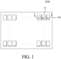
- FIG. 1 is a plan view illustrating an organic light emitting display (OLED) device 1000 according to an exemplary embodiment of the present disclosure
- FIG. 2 is a cross-sectional view taken along a line I-I' of FIG. 1 .
- OLED organic light emitting display
- an OLED device 1000 includes a plurality of pixels P1, P2, and P3 adjacent to each other.
- a pixel refers to a minimum unit that actually emits a light, and may also be referred to as a sub-pixel or a pixel region. Further, a plurality of pixels may form a minimum group capable of expressing a white light.
- FIG. 1 illustrates a first pixel P1, a second pixel P2, and a third pixel P3 as a single group "A", but is not necessarily limited thereto.
- the pixels may be designed in various ways.
- the plurality of pixels P1, P2, and P3 forming a single group emit lights of different colors. For example, according to a pixel design, the plurality of pixels P1, P2, and P3 may emit a red (R) light, a green (G) light, and a blue (B) light, respectively, as illustrated in FIG. 2 .
- each pixel includes a thin film transistor (TFT) 300 and an organic light emitting element 400.
- the TFT 300 is disposed on a substrate 100 and configured to supply a signal to the organic light emitting element 400.
- the TFT 300 shown in FIG. 2 may be a driving thin film transistor connected to a first electrode 410 of the organic light emitting element 400.
- each of the pixels P1, P2, and P3 may further include a switching thin film transistor or a capacitor for driving the organic light emitting element 400.
- the substrate 100 may be formed of an insulation material.
- the substrate 100 may be formed of a glass or may be formed into a flexible film formed of polyimide-based material.
- the TFT 300 includes a gate electrode 310, an active layer 320, a source electrode 330, and a drain electrode 340.
- the gate electrode 310 is formed on the substrate 100, and a gate insulation layer 210 covers the gate electrode 310.
- the active layer 320 is disposed on the gate insulation layer 210 so as to be overlapped with the gate electrode 310.
- the source electrode 330 and the drain electrode 340 are disposed to be spaced apart from each other on the active layer 320.
- an overlap of two objects may mean that at least parts of the two objects are overlapped in a vertical relation between the two objects regardless of whether or not another object is present therebetween, and may also be referred to using various other terms.
- the gate electrode 310, the source electrode 330, and the drain electrode 340 are formed of conductive materials. They may be formed of, for example, any one of molybdenum (Mo), aluminum (Al), chromium (Cr), gold (Au), titanium (Ti), nickel (Ni), neodymium (Nd), and copper (Cu) or alloys thereof, but are not limited thereto, and may be formed of various materials.
- Mo molybdenum
- Al aluminum
- Cr chromium
- Au gold
- Ti titanium
- Ni nickel
- Nd neodymium
- Cu copper
- the active layer 320 may be formed of any one of amorphous silicon (a-Si), polycrystalline silicon (poly-Si), oxide, and an organic material according to a kind of the active layer 320, but is not limited thereto.
- a-Si amorphous silicon
- poly-Si polycrystalline silicon
- oxide an organic material according to a kind of the active layer 320, but is not limited thereto.
- the gate insulation layer 210 may include a single layer or a plurality of layers formed of an inorganic material, and may be formed of silicon oxide (SiO x ), silicon nitride (SiN x ), and the like.
- FIG. 2 illustrates the TFT 300 as having a staggered structure, but is not limited thereto.
- the TFT 300 may have a coplanar structure.
- a planarization layer 220 that exposes a part of the source electrode 330 is disposed on the TFT 300.
- the planarization layer 220 may include a single layer or a plurality of layers and may be formed of an organic material. To be specific, the planarization layer 220 may be formed of polyimide, acryl, and the like.
- a passivation layer may be further formed between the planarization layer 220 and the TFT 300.
- the passivation layer may be formed of an inorganic material, may protect the TFT 300, and may also expose a part of the source electrode 330 in the same manner as the planarization layer 220.
- the organic light emitting element 400 is disposed on the planarization layer 220, and includes the first electrode 410, a light emitting unit 420, and a second electrode 430.
- the OLED device 1000 according to an exemplary embodiment of the present disclosure is an OLED device of a top-emission type, and, thus, a light emitted by the light emitting unit 420 penetrates the second electrode 430 and is emitted in an upward direction.
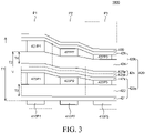
- FIG. 3 is a cross-sectional view illustrating main components of the portion A illustrated in FIG. 1 .
- FIG. 3 is a cross-sectional view explaining a structure of the organic light emitting element 400 of the plurality of pixels P1, P2, and P3 adjacent to each other in a single group.
- a plurality of first electrodes 410P1, 410P2, and 410P3 are disposed to be spaced apart from each other and correspond to the respective pixels P1, P2, and P3.
- the plurality of first electrodes 410P1, 410P2, and 410P3 is configured to supply holes to light emitting layers 423 and 427 of the light emitting unit 420.
- Each of the plurality of first electrodes 410P1, 410P2, and 410P3 is connected to the source electrode 330 of the TFT 300.
- the plurality of first electrodes 410P1, 410P2, and 410P3 are referred to as anodes.
- the first electrode 410 may be connected to the drain electrode 340 according to a kind of the TFT 300.
- the plurality of first electrodes 410P1, 410P2, and 410P3 may include a reflective layer.
- the first electrode 410 may have a two-layer structure including a transparent layer and a reflective layer stacked in sequence, or a three-layer structure including a transparent layer, a reflective layer, and a transparent layer stacked in sequence.
- the transparent layer may be formed of a transparent conductive oxide (TCO) material such as indium tin oxide (ITO) or indium zinc oxide (IZO).
- the reflective layer may be formed of a metal material such as copper (Cu), silver (Ag), and palladium (Pd).
- the second electrode 430 is disposed commonly throughout the plurality of pixels P1, P2, and P3, and configured to supply electrons to the light emitting layers 423 and 427 of the light emitting unit 420.
- the second electrode 430 needs to transmit a light from the light emitting unit 420.
- the second electrode 430 may be formed of a metal material having a very small thickness, for example, from 150 ⁇ to 250 ⁇ , or a transparent material.
- the second electrode 430 may be formed of, for example, silver (Ag), magnesium (Mg), indium zinc oxide (IZO), indium tin oxide (ITO), and the like.
- the second electrode 430 is referred to as a cathode.
- the OLED device 1000 includes a first light emitting unit 420a, a second light emitting unit 420b, and a charge generation layer 425 between the first electrode 410 and the second electrode 430 as shown in FIG. 3 .
- the first light emitting unit 420a includes a hole injection layer 421, a first hole transporting layer 422, a first light emitting layer 423, and a first electron transporting layer 424.
- the hole injection layer 421 is disposed on the first electrode 410 and smoothly injects holes supplied from the first electrode 410 to the first light emitting layer 423.
- the hole injection layer 421 may be formed of 4,4',4"-tris(3-methylphenylphenylamino)triphenylamine (MTDATA), copper phthalocyanine (CuPc), or poly(3,4-ethylenedioxythiphene, polystyrene sulfonate (PEDOT/PSS), but is not necessarily limited thereto. Further, the hole injection layer 421 may have a thickness of from about 30 ⁇ to about 100 ⁇ .
- the first hole transporting layer 422 is disposed on the hole injection layer 421 and smoothly transports holes supplied from the first electrode 410 to the first light emitting layer 423.
- the first hole transporting layer 422 may be formed of N,N'-diphenyl-N,N'-bis(3-methylphenyl)-1,1'-bi-phenyl-4,4'-diamine (TPD) or N,N'-di(naphthalen-1-yl)-N,N'-diphenyl-benzidine (NPB), but is not necessarily limited thereto.
- the first electron transporting layer 424 is disposed on the first light emitting layer 423 and smoothly transports electrons supplied from the charge generation layer 425 to the first light emitting layer 423.
- the first electron transporting layer 424 may be formed of oxadiazole, triazole, phenanthroline, benzoxazole, benzthiazole, or the like, but is not necessarily limited thereto. Further, the first electron transporting layer 424 may have a thickness of from about 50 ⁇ to about 200 ⁇ .
- the hole injection layer 421, the first hole transporting layer 422 and the first electron transporting layer 424 have a common structure each disposed throughout the plurality of pixels P1, P2, and P3.
- each of the hole injection layer 421, the first hole transporting layer 422 and the first electron transporting layer 424 is extended on the plurality of first electrodes 410P1, 410P2, and 410P3 corresponding to the first pixel P1, the second pixel P2, and the third pixel P3.
- the layers having the common structure are formed into the same shape in the pixels P1, P2, and P3 without patterning for each of the pixels P1, P2, and P3.
- the layers may be deposited using a common mask open to all of the pixels P1, P2, and P3.
- the first light emitting layer 423 has a patterned structure divided for each of the pixels P1, P2, and P3.
- a first light emitting layer 423P1 of the first pixel P1 is disposed to be overlapped with the first electrode 410P1 of the first pixel P1, and may emit, for example, a red light.
- a first light emitting layer 423P2 of the second pixel P2 is disposed to be overlapped with the first electrode 410P2 of the second pixel P2, and may emit, for example, a green light.
- a first light emitting layer 423P3 of the third pixel P3 is disposed to be overlapped with the first electrode 410P3 of the third pixel P3, and may emit, for example, a blue light.
- the light emitting layers 423P1, 423P2, and 423P3 emitting lights of different colors are patterned for the pixels P1, P2, and P3, respectively.
- the first light emitting layer 423 may be deposited and patterned using a mask, for example, a fine metal mask (FMM), open and divided for each of the pixels P1, P2, and P3.
- the first patterned light emitting layers 423P1, 423P2, and 423P3 may have different heights with respect to each other.
- the first electron transporting layer 424 may be positioned between the first patterned light emitting layers 423P1, 423P2 and 423P3.
- the second light emitting unit 420b is disposed between the first light emitting unit 420a and the second electrode 430.
- the second light emitting unit 420b includes a second hole transporting layer 426, a second light emitting layer 427, and a second electron transporting layer 428.
- the second hole transporting layer 426 is disposed on the charge generation layer 425 and smoothly transports holes supplied from the charge generation layer 425 to the second light emitting layer 427.
- the second electron transporting layer 428 is disposed on the second light emitting layer 427 and smoothly transports electrons supplied from the second electrode 430 to the second light emitting layer 427.
- the second electron transporting layer 428 may be formed of oxadiazole, triazole, phenanthroline, benzoxazole, or benzthiazole, but is not necessarily limited thereto. Further, the second electron transporting layer 428 may have a thickness of from about 250 ⁇ to about 350 ⁇ .
- the second hole transporting layer 426 and the second electron transporting layer 428 have a common structure each disposed throughout the plurality of pixels P1, P2, and P3 in the same manner as the hole injection layer 421, the first hole transporting layer 422, and the first electron transporting layer 424.
- the second hole transporting layer 426 and the second electron transporting layer 428 are formed into the same shape in the pixels P1, P2, and P3 without patterning for each of the pixels P1, P2, and P3.
- the second light emitting layer 427 has a patterned structure divided for each of the pixels P1, P2, and P3 in the same manner as the first light emitting layer 423.
- the second patterned light emitting layers 427P1, 427P2, and 427P3 may have different heights with respect to each other.
- the second light emitting layer 427 emits a light of the same color as a light emitted by the first light emitting layer 423.
- the first light emitting layer 423P1 and a second light emitting layer 427P1 of the first pixel P1 may emit lights of the same color, for example, red lights.
- the first light emitting layer 423P1 and the second light emitting layer 427P1 of the first pixel P1 emit lights having the same peak wavelength.
- Each of the first light emitting layer 423P1 and the second light emitting layer 427P1 may have a peak wavelength from 600 nm to 650 nm. In this case, even if the first light emitting layer 423P1 and the second light emitting layer 427P1 do not have exactly the same peak wavelength, these layers can be regarded as emitting lights of the same color. If the first light emitting layer 423P1 and the second light emitting layer 427P1 of the first pixel P1 are light emitting layers emitting red lights, the first pixel P1 is a red pixel.
- the first light emitting layer 423P2 and a second light emitting layer 427P2 of the second pixel P2 may emit lights of the same color, for example, green lights.
- the first light emitting layer 423P2 and the second light emitting layer 427P2 of the second pixel P2 emit lights having the same peak wavelength.
- Each of the first light emitting layer 423P2 and a second light emitting layer 427P2 may have a peak wavelength from 540 nm to 580 nm. In this case, even if the first light emitting layer 423P2 and a second light emitting layer 427P2 do not have exactly the same peak wavelength, these light emitting layers can be regarded as emitting lights of the same color. If the first light emitting layer 423P2 and a second light emitting layer 427P2 of the second pixel P2 are light emitting layers emitting green lights, the second pixel P2 is a green pixel.
- the first light emitting layer 423P3 and a second light emitting layer 427P3 of the third pixel P3 may emit lights of the same color, for example, blue lights.
- the first light emitting layer 423P3 and the second light emitting layer 427P3 of the third pixel P3 emit lights having the same peak wavelength.
- Each of the first light emitting layer 423P3 and the second light emitting layer 427P3 may have a peak wavelength from 440 nm to 480 nm. In this case, even if the first light emitting layer 423P3 and the second light emitting layer 427P3 do not have exactly the same peak wavelength, these light emitting layers can be regarded as emitting lights of the same color. If the first light emitting layer 423P3 and the second light emitting layer 427P3 of the third pixel P3 are light emitting layers emitting blue lights, the third pixel P3 is a blue pixel.
- the hole injection layer 421, the first hole transporting layer 422, the first electron transporting layer 424, the second hole transporting layer 426 and the second electron transporting layer 428 have a common structure each disposed throughout the plurality of pixels P1, P2, and P3. Therefore, they may be referred to as a common hole injection layer 421, a first common hole transporting layer 422, a first common electron transporting layer 424, a second common hole transporting layer 426, and a second common electron transporting layer 428, respectively.
- the first light emitting layer 423 and the second light emitting layer 427 have a patterned structure divided for each of the pixels P1, P2, and P3. Therefore, they may be referred to as a plurality of first patterned light emitting layers 423 and a plurality of second patterned light emitting layers 427, respectively.
- the charge generation layer 425 is disposed between the first light emitting unit 420a and the second light emitting unit 420b.
- the charge generation layer 425 controls a balance of charges between the first light emitting unit 420a and the second light emitting unit 420b.
- the charge generation layer 425 may include an N-type charge generation layer 425n and a P-type charge generation layer 425p.
- the N-type charge generation layer 425n is disposed adjacent to the first light emitting unit 420a and supplies electrons to the first light emitting unit 420a.
- the N-type charge generation layer 425n may be formed into an organic layer doped with alkali metal such as lithium (Li), sodium (Na), potassium (K), or cesium (Cs), or alkali earth metal such as magnesium (Mg), strontium (Sr), barium (Ba), or radium (Ra), but is not necessarily limited thereto. Further, the N-type charge generation layer 425n may have a thickness of from about 50 ⁇ to about 200 ⁇ .
- the P-type charge generation layer 425p is disposed adjacent to the second light emitting unit 420b and supplies holes to the second light emitting unit 420b.
- the P-type charge generation layer 425p may be formed into an organic layer including a P-type dopant, but is not necessarily limited thereto. Further, the P-type charge generation layer 425p may have a thickness of from about 30 ⁇ to about 100 ⁇ .
- the first hole transporting layer 422 of the first light emitting unit 420a and the second hole transporting layer 426 of the second light emitting unit 420b have a thickness ratio.
- the thickness ratio is for minimizing an increase in driving voltage caused by a shift of an emission zone in the first light emitting layer 423 or in the second light emitting layer 427 due to prolonged driving of the OLED device 1000.
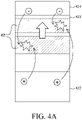
- An emission zone EZ refers to a portion or a region where recombination of holes supplied from the first electrode 410 or the charge generation layer 425 and electrons supplied from the second electrode 430 or the charge generation layer 425 intensively occurs within the light emitting layers 423 and 427.
- the emission zone EZ may be shifted due to prolonged driving of the OLED device 1000.
- the emission zone EZ may be formed at a central part of the light emitting layer 423.
- the emission zone EZ may be shifted toward an upper part of the light emitting layer 423 or toward the first electron transporting layer 424 as another organic layer adjacent to the light emitting layer 423 due to prolonged driving.
- an interface between the light emitting layer 423 and the first electron transporting layer 424 may be degraded.
- Such a change in characteristic causes an increase in driving voltage of the OLED device 1000. Therefore, power consumption of the OLED device 1000 is increased and a lifetime of the OLED device 1000 is decreased.
- the emission zone EZ may be one-sided at a lower part with respect to the central part of the light emitting layer 423.
- a shift distance of the emission zone EZ toward the first electron transporting layer 424 is increased.
- a time for the emission zone EZ and the first electron transporting layer 424 to be close to each other is increased. That is, it is possible to reduce a change in characteristic of the interface between the light emitting layer 423 and the first electron transporting layer 424 caused by a shift of the emission zone EZ even in the case of prolonged driving.
- FIG. 4A and FIG. 4B illustrate that the emission zone EZ is shifted in an upward direction, for example, a direction being close to the first electron transporting layer 424.
- the emission zone EZ may be shifted in a downward direction, for example, a direction being close to the first hole transporting layer 422, according to peak wavelengths of lights emitted from the light emitting layers 423 and 427 or thicknesses of the layers between the two electrodes 410 and 430.
- the emission zone EZ in the first light emitting layer 423 or in the second light emitting layer 427 may be one-sided at an upper part or a lower part with respect to the central part of the first light emitting layer 423 or in the second light emitting layer 427.
- a thickness T4 of the second hole transporting layer 426 is greater than a thickness T3 of the first hole transporting layer 422 as shown.
- a thickness ratio T3: T4 of the first hole transporting layer 422 and the second hole transporting layer 426 is from 1:1.25 to 1:1.5. Therefore, the emission zone EZ can be one-sided at an upper part or a lower part within the first light emitting layer 423 or in the second light emitting layer 427.
- the first hole transporting layer 422 and the second hole transporting layer 426 may be formed of the same material.
- the hole transporting layers 422 and 426 When controlling thicknesses of the other organic layers, for example, the electron transporting layers 424 and 428 or the hole injection layer 421, than the hole transporting layers 422 and 426, characteristics, such as a driving voltage or a driving current, of the OLED device 1000 may be greatly changed. Thus, it may become difficult to manage a deviation or a defect during a manufacturing process. When comparing with the other organic layers, the hole transporting layers 422 and 426 less affect the characteristics of the OLED device 1000. Therefore, locations of the emission zones EZ within the light emitting layers 423 and 427 may be controlled by controlling the thicknesses T3 and T4 of the hole transporting layers 422 and 426, respectively.
- the sum of the thickness T3 of the first hole transporting layer 422 and the thickness T4 of the second hole transporting layer 426 may be from 750 ⁇ to 1,150 ⁇ .
- the thickness T3 of the first hole transporting layer 422 may be from 350 ⁇ to 550 ⁇
- the thickness T4 of the second hole transporting layer 426 may be from 400 ⁇ to 600 ⁇ .
- the respective thicknesses T3 and T4 of the first hole transporting layer 422 and the second hole transporting layer 426 and the sum (T3+T4) of the thicknesses are in the above-described ranges. Therefore, the emission zone EZ can be one-sided at an upper part or a lower part within the first light emitting layer 423 or within the second light emitting layer 427.
- the hole transporting layers 422 and 426 are too thin, their capability of transporting holes to the light emitting layers 423 and 427 may be decreased. Thus, the light efficiency of the OLED 1000 may be decreased. Furthermore, if the hole transporting layers 422 and 426 are too thick, a thickness of the OLED device 1000 may be increased or a time for forming the hole transporting layers 422 and 426 may be increased. Thus, a process tack time may be increased.
- a distance T1 between the first electrode 410 and the second electrode 430 may have a value, which results in constructive interference being generated between light emitted from the first light emitting layer 423 and a light emitted from the second light emitting layer 427 due to micro-cavity effects.
- the first electrode 410 may include a transparent conductive layer formed of ITO or IZO and a reflective layer formed of a metal material.
- the distance T1 from a top surface of the reflective layer to a bottom surface of the second electrode 430 is the distance T1 between the first electrode 410 and the second electrode 430.
- the micro-cavity effect refers to an improvement in light efficiency since lights emitted from the light emitting layers 423 and 427 are amplified between the two electrodes 410 and 430 through repeated reflection and re-reflection and constructive interference is thus generated.
- initial locations of the emission zones EZ may vary depending on peak wavelengths of lights emitted from the light emitting layers 423 and 427 and thicknesses of the layers between the two electrodes 410 and 430.
- the light efficiency can be improved only when the emission zone EZ is located at a portion where constructive interference between lights emitted from the two light emitting layers 423 and 427 is generated due to the micro-cavity effects.
- the thickness T4 of the second hole transporting layer 426 is greater than the thickness T3 of the first hole transporting layer 422 according to an exemplary embodiment of the present disclosure.
- the distance T1 between the first electrode 410 and the second electrode 430 is from 1,700 ⁇ to 3,000 ⁇ , locations of the emission zones EZ within the light emitting layers 423 and 427 are optimized.
- constructive interference between a light emitted from the first light emitting layer 423 and light emitted from the second light emitting layer 427 is effectively generated due to micro-cavity effects. Therefore, the light efficiency of the OLED 1000 can be improved.
- the distance T1 between the first electrode 410 and the second electrode 430 is determined considering peak wavelengths of lights emitted from the first light emitting layer 423 and the second light emitting layer 427.
- the first light emitting layers 423P1, 423P2, and 423P3 patterned and disposed in the respective pixels P1, P2, and P3 emit lights of different colors for the respective pixels P1, P2, and P3.
- the second light emitting layers 427P1, 427P2, and 427P3 patterned and disposed in the respective pixels P1, P2, and P3 emit lights of different colors for the respective pixels P1, P2, and P3.
- a distance between the first electrode 410P1 of the first pixel P1 and the second electrode 430, a distance between the first electrode 410P2 of the second pixel P2 and the second electrode 430, and a distance between the first electrode 410P3 of the third pixel P3 and the second electrode 430 may be different from each other.
- the distance T1 between the two electrodes 410 and 430 in each of the pixels P1, P2, and P3 may be controlled using the thicknesses of the first light emitting layer 423 and the second light emitting layer 427, which are patterned and formed in each of the pixels P1, P2, and P3.
- the height of the first patterned light emitting layers 423P1, 423P2, 423P3 and the height of the second patterned light emitting layers 427P1, 427P2, 427P3 may be different for the respective pixels P1, P2, P3. Further, the second patterned light emitting layers 427P1, 427P2, and 427P3 may have a same height, respectively, as the corresponding first patterned light emitting layers 423P1, 423P2, and 423P3, or not.
- the first pixel P1 may be a red pixel.
- each of the first light emitting layer 423P1 and the second light emitting layer 427P1 emitting lights of the same color may have a thickness of from 450 ⁇ to 750 ⁇ , which results in constructive interference being generated between the two electrodes 410P1 and 430 due to micro-cavity effects.
- the second pixel P2 may be a green pixel.
- each of the first light emitting layer 423P2 and the second light emitting layer 427P2 emitting lights of the same color may have a thickness of from 300 ⁇ to 500 ⁇ , which results in constructive interference being generated between the two electrodes 410P2 and 430 due to micro-cavity effects.
- the third pixel P3 may be a blue pixel.
- each of the first light emitting layer 423P3 and the second light emitting layer 427P3 emitting lights of the same color may have a thickness of from 100 ⁇ to 300 ⁇ , which results in constructive interference being generated between the two electrodes 410P3 and 430 due to micro-cavity effects.
- the distance T2 between the two light emitting layers 423 and 427 in each of the pixels P1, P2, and P3 is also from 500 ⁇ to 750 ⁇ .
- the distance T2 between the two light emitting layers 423 and 427 emitting lights of the same color in the same pixel is from 500 ⁇ to 750 ⁇ .
- the thickness T4 of the second hole transporting layer 426 is preferably greater than the thickness of the electron transporting layer 424 to balance the supplies of electrons and holes.
- the OLED device 1000 includes the first light emitting unit 420a including the first patterned light emitting layer 423 and the first common hole transporting layer 422 and the second light emitting unit 420b including the second patterned light emitting layer 427 and the second common hole transporting layer 426 according to an exemplary embodiment of the present disclosure.
- the thickness T4 of the second common hole transporting layer 426 is greater than the thickness T3 of the first common hole transporting layer 422.
- the thickness ratio of the first hole transporting layer to the second hole transporting layer is within a range from 1:1.25 to 1:1.5.
- the first and second common hole transporting layers 422 and 426 respectively included in the first light emitting unit 420a and the second light emitting unit 420b are formed of the same material.
- the thickness T3 of the first common hole transporting layer 422 included in the first light emitting unit 420a, i.e., the hole transporting layer 422 disposed close to the first electrode 410 or the anode, is smaller than the thickness T4 of the second common hole transporting layer 426 included in the second light emitting unit 420b.
- the thickness ratio of the first hole transporting layer to the second hole transporting layer is within a range from 1:1.25 to 1:1.5.
- FIG. 5 through FIG. 7 are graphs illustrating results of evaluation on a lifetime according to Comparative Examples and Example of the present disclosure.
- FIG. 5 is a graph illustrating a result of evaluation on a lifetime of the above-described structure according to Comparative Examples and Example. Referring to Table 1, a thickness of any one of the first hole transporting layer 422 and the second hole transporting layer 426 is assumed as 100% and a thickness of the other is compared and expressed.
- Thickness (T3) of first hole transporting layer Thickness (T4) of second hole transporting layer Thickness ratio (T3:T4) Example 80% 100% 1:1.25 Comparative Example 1 100% 80% 1:0.8 Comparative Example 2 100% 50% 1:0.5
- the thickness T4 of the second hole transporting layer is greater than the thickness T3 of the first hole transporting layer in a structure according to Example.
- a thickness ratio T3:T4 of the first hole transporting layer to the second hole transporting layer is 1:1.25 in this structure.
- the thickness T4 of the second hole transporting layer is smaller than the thickness T3 of the first hole transporting layer in structures according to Comparative Example 1 and Comparative Example 2.
- thickness ratios T3:T4 of the first hole transporting layer to the second hole transporting layer are 1:0.8 and 1:0.5 in these structures.
- the thickness of the second hole transporting layer is greater than the thickness of the first hole transporting layer.
- the thickness ratio of the first hole transporting layer to the second hole transporting layer is within a range from 1:1.25 to 1:1.5.
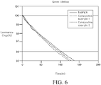
- FIG. 6 is a graph illustrating a result of evaluation on a lifetime of the above-described structure according to Comparative Examples and Example.
- the thickness T4 of the second hole transporting layer is greater than the thickness T3 of the first hole transporting layer in a structure according to Example.
- the thickness ratio of the first hole transporting layer to the second hole transporting layer is within a range from 1:1.25 to 1:1.5.
- the thickness T4 of the second hole transporting layer is smaller than the thickness T3 of the first hole transporting layer in structures according to Comparative Example 1 and Comparative Example 2.
- the thickness of the second hole transporting layer is greater than the thickness of the first hole transporting layer.
- the thickness ratio of the first hole transporting layer to the second hole transporting layer is within a range from 1:1.25 to 1:1.5.
- FIG. 7 is a graph illustrating a result of evaluation on a lifetime of the above-described structure according to Comparative Examples and Example.
- the thickness T4 of the second hole transporting layer is greater than the thickness T3 of the first hole transporting layer in a structure according to Example.
- the thickness ratio of the first hole transporting layer to the second hole transporting layer is within a range from 1:1.25 to 1:1.5.
- the thickness T4 of the second hole transporting layer is smaller than the thickness T3 of the first hole transporting layer in structures according to Comparative Example 1 and Comparative Example 2.
- the thickness of the second hole transporting layer is greater than the thickness of the first hole transporting layer.
- the thickness ratio of the first hole transporting layer to the second hole transporting layer is within a range from 1:1.25 to 1:1.5.
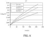
- FIG. 8 is a graph illustrating a result of evaluation on delta voltage according to Comparative Examples and Example of the present disclosure. If the plurality of patterned light emitting layers 423 and 427 emit blue lights, the thickness T3 of the first hole transporting layer 422 and the thickness T4 of the second hole transporting layer 426 may be applied as listed in the above Table 1 to the structure illustrated in FIG. 5 .
- FIG. 8 is a graph illustrating a result of evaluation on a delta voltage ⁇ V of the above-described structure according to Comparative Examples and Example. The delta voltage exhibits a difference between an initial driving voltage and a driving voltage changed according to a time. An increase in delta voltage means that a driving voltage is increased that much.
- a delta voltage was about 0.2 V after the OLED device was driven for about 150 hrs. That is, it can be seen that a driving voltage was increased by about 0.2 V as compared with an initial driving voltage.
- the thickness of the second hole transporting layer is greater than the thickness of the first hole transporting layer.
- the thickness ratio of the first hole transporting layer to the second hole transporting layer is within a range from 1:1.25 to 1:1.5.
- the first hole transporting layer and the second hole transporting layer have a thickness ratio for minimizing an increase in driving voltage caused by shifts of emission zones in a plurality of patterned light emitting layers due to prolonged driving. Therefore, it is possible to solve a problem of an increase in power consumption of the OLED device and thus possible to improve a lifetime of the OLED device.
- the thickness of the second hole transporting layer is greater than the thickness of the first hole transporting layer.
- the thickness ratio of the first hole transporting layer to the second hole transporting layer is within a range from 1:1.25 to 1:1.5. Therefore, it is possible to minimize an increase in delta voltage or driving voltage of the OLED device even in the case of prolonged driving.
Description
- The present disclosure relates to an organic light emitting display device. More particularly, the disclosure relates to an organic light emitting display device having longer lifetime by minimizing an increase in driving voltage of an organic light emitting element according to time and thus solving a problem of an increase in power consumption.
- An organic light emitting display (OLED) device is a next-generation display device having a self-luminance characteristic. The OLED device does not need a separate light source, unlike a liquid crystal display device. Thus, the OLED device can be manufactured into a lightweight and thin form. Further, the OLED device is advantageous in terms of a viewing angle, contrast, a response speed, power consumption, and the like. Therefore, the OLED device has received much attention as a next-generation display device.
-
US 2015/0188087 A1 relates to an organic light emitting display device including a first electrode defined into red, green and blue sub-pixel regions; a first light emitting unit disposed on the first electrode and configured with a hole injection layer, a first hole transport layer, a first organic emission layer and a first electron transport layer. The known device further includes a second light emitting unit disposed on the first light emitting unit and configured with a second hole transport layer, a second organic emission layer and a second electron transport layer; and a second electrode disposed on the second light emitting unit. A separation between the first organic emission layer and the second organic emission layer is larger than a separation between the first electrode and the first organic emission layer. -
US 2015/0194471 A1 describes an organic light emitting display device having excellent lifespan and current efficiency characteristics, as well as high luminance to provide increased resolution and improved reliability, and a method for manufacturing the same. The known organic light emitting display device comprises a substrate having first, second, and third pixel regions; a first electrode arranged on the substrate; a second electrode arranged on the first electrode; and an organic layer arranged between the first electrode and the second electrode. The organic layer includes first, second and third organic layers on the first, second and third pixel regions, respectively. Each of the first, second and third organic layers includes a plurality unit organic layers and at least one charge generating layer arranged between the plurality of unit organic layers. - An organic light emitting display (OLED) device is a display device in which holes and electrons are respectively injected from two electrodes and recombined into excitons in a light emitting layer and the excitons emit a light having a specific wavelength during energy release. The OLED device has a self-luminance characteristic.
- However, the OLED device has a problem of a shorter lifetime than other display devices such as a liquid crystal display device. To be specific, if the OLED device is driven for a long time, an emission zone in the light emitting layer where recombination of the holes and the electrons intensively occurs is shifted toward another organic layer adjacent to the light emitting layer. In this case, an interface between the light emitting layer and the organic layer adjacent to the light emitting layer as well as the light emitting layer may be degraded. Such a change in characteristic causes an increase in driving voltage of the OLED device. Therefore, power consumption of the OLED device is increased and a lifetime of the OLED device is decreased.
- Accordingly, the inventors of the present invention recognized the above-described problems and conducted various experiments for reducing an increase in driving voltage caused by a shift of an emission zone. The inventors of the present invention optimized a structure of organic layers, particularly, a hole transporting layer, between two electrodes through the various experiments. Then, the inventors of the present invention invented a new OLED device with improved power consumption.
- Accordingly, an advantage of the present disclosure is to provide an OLED device having improved power consumption and improved lifetime by configuring a plurality of hole transporting layers to have a thickness ratio for minimizing an increase in driving voltage caused by a shift of an emission zone due to prolonged driving.
- The advantages of the present disclosure are not limited to the aforementioned advantages, and other advantages, which are not mentioned above, will be apparent to a person having ordinary skill in the art from the following description.
- Said object has been addressed with the subject-matter of the independent claim. Advantageous embodiments are described in the dependent claims. Preferably, the sum of the thickness of the first hole transporting layer and the thickness of the second hole transporting layer is from 750 Å to 1,150 Å. Preferably, the first hole transporting layer and the second hole transporting layer are formed of the same material. Preferably, a distance between the first electrode and the second electrode is from 1,700 Å to 3,000 Å. This results in constructive interference being generated between light emitted from the first light emitting layer and light emitted from the second light emitting layer due to micro-cavity effects. Preferably, a distance between the first light emitting layer and the second light emitting layer is from 500 Å to 750 Å. Preferably, the first light emitting layer and the second light emitting layer have a patterned structure divided for each pixel, respectively, and the first hole transporting layer and the second hole transporting layer have a common structure disposed throughout a plurality of pixels, respectively.
- According to another aspect of the present disclosure, there is provided an OLED device of a top-emission type that includes a plurality of pixels adjacent to each other. The OLED device comprises: a plurality of first electrodes respectively corresponding to the plurality of pixels and spaced apart from each other; and a first common hole transporting layer on the plurality of first electrodes. Further, the OLED device includes: a plurality of first patterned light emitting layers on the first common hole transporting layer corresponding to the plurality of pixels respectively; a second common hole transporting layer on the plurality of first patterned light emitting layers that has a greater thickness than the first common hole transporting layer; a plurality of second patterned light emitting layers on the second common hole transporting layer corresponding to the plurality of pixels respectively; and a second electrode on the plurality of second patterned light emitting layers. A thickness ratio of the first common hole transporting layer to the second common hole transporting layer is from 1:1.25 to 1:1.5. Preferably, the first common hole transporting layer and the second common hole transporting layer are formed of the same material. Preferably, the sum of the thickness of the first common hole transporting layer and the thickness of the second common hole transporting layer is from 750 Å to 1,150 Å. Preferably, in each of the plurality of pixels, a distance between the first electrode and the second elec-trode is from 1,700 Å to 3,000 Å, which results in constructive interference being generated between a light emitted from the first patterned light emitting layer and a light emitted from the second patterned light emitting layer due to micro-cavity effects. Preferably, a distance between the first patterned light emitting layer and the second patterned light emit-ting layer is from 500 Å to 750 Å.
- A first hole transporting layer and a second hole transporting layer have a thickness ratio for minimizing an increase in driving voltage caused by a shift of an emission zone in a first light emitting layer or a second light emitting layer due to prolonged driving. Therefore, it is possible to solve a problem of an increase in power consumption of an OLED device and thus possible to improve a lifetime of the OLED device.
- The thickness ratio of the first hole transporting layer and the second hole transporting layer results in the emission zone to be biased toward an upper part or a lower part with respect to a central part of the light emitting layer. Therefore, it is possible to solve a problem of an increase in driving voltage or delta voltage of the OLED device.
- Among two hole transporting layers formed of the same material, a hole transporting layer disposed closer to an anode has a smaller thickness than the other hole transporting layer. Therefore, it is possible to minimize an increase in driving voltage of the OLED device even in the case of prolonged driving.
- A distance between two electrodes and a distance between two light emitting layers emitting lights of the same color are optimized. Therefore, it is possible to generate constructive interference due to micro-cavity effects of the light emitting layers and thus possible to improve a light efficiency and a lifetime of the OLED.
- The effects of the present disclosure are not limited to the aforementioned effects, and other effects, which are not mentioned above, will be apparent to a person having ordinary skill in the art from the following description.
- The above and other aspects, features and other advantages of the present disclosure will be more clearly understood from the following detailed description taken in conjunction with the accompanying drawings, in which:
-
FIG. 1 is a plan view illustrating an OLED device according to an exemplary embodiment of the present disclosure; -
FIG. 2 is a cross-sectional view taken along a line I-I' ofFIG. 1 ; -
FIG. 3 is a cross-sectional view illustrating main components of a portion A illustrated inFIG. 1 ; -
FIG. 4A andFIG. 4B are schematic cross-sectional views explaining a shift of an emission zone in a light emitting layer; -
FIG. 5 through FIG. 7 are graphs illustrating results of evaluation on a lifetime according to Comparative Examples and Example of the present disclosure; and -
FIG. 8 is a graph illustrating a result of evaluation on delta voltage according to Comparative Examples and Example of the present disclosure. - Advantages and features of the present disclosure, and methods for accomplishing the same will be more clearly understood from exemplary embodiments described below with reference to the accompanying drawings. However, the present disclosure is not limited to the following exemplary embodiments but may be implemented in various different forms. The exemplary embodiments are provided only to complete disclosure of the present disclosure and to fully provide a person having ordinary skill in the art to which the present disclosure pertains with the category of the disclosure, and the scope of the present invention is defined by the appended claims.
- The shapes, sizes, ratios, angles, numbers, and the like shown in the accompanying drawings for describing the exemplary embodiments of the present disclosure are merely examples, and the present disclosure is not limited thereto. Like reference numerals generally denote like elements throughout the present specification. Further, in the following description, a detailed explanation of known related technologies may be omitted to avoid unnecessarily obscuring the subject matter of the present disclosure.
- The terms such as "including," "having," and "consist of' used herein are generally intended to allow other components to be added unless the terms are used with the term "only". Any references to singular may include plural unless expressly stated otherwise.
- Components are interpreted to include an ordinary error range even if not expressly stated.
- When the position relation between two parts is described using the terms such as "on", "above", "below", and "next", one or more parts may be positioned between the two parts unless the terms are used with the term "immediately" or "directly" is not used.
- When the time sequence between two or more incidents is described using the terms such as "after", "subsequent to", "next to", and "before", two or more incidents may be inconsecutive unless the terms are used with the term "immediately" or "directly".
- Although the terms "first", "second", and the like are used for describing various components, these components are not confined by these terms. These terms are merely used for distinguishing one component from the other components. Therefore, a first component to be mentioned below may be a second component in a technical concept of the present disclosure.
- Since size and thickness of each component shown in the drawings are represented for convenience in explanation, the present disclosure is not necessarily limited to the shown size and thickness of each component.
- The features of various embodiments of the present disclosure can be partially or entirely bonded to or combined with each other and can be interlocked and operated in technically various ways, and the embodiments can be carried out independently of or in association with each other.
- Hereinafter, exemplary embodiments of the present disclosure will be described in detail with reference to the accompanying drawings.
-
FIG. 1 is a plan view illustrating an organic light emitting display (OLED)device 1000 according to an exemplary embodiment of the present disclosure, andFIG. 2 is a cross-sectional view taken along a line I-I' ofFIG. 1 . - Referring to
FIG. 1 andFIG. 2 , anOLED device 1000 includes a plurality of pixels P1, P2, and P3 adjacent to each other. A pixel refers to a minimum unit that actually emits a light, and may also be referred to as a sub-pixel or a pixel region. Further, a plurality of pixels may form a minimum group capable of expressing a white light.FIG. 1 illustrates a first pixel P1, a second pixel P2, and a third pixel P3 as a single group "A", but is not necessarily limited thereto. The pixels may be designed in various ways. The plurality of pixels P1, P2, and P3 forming a single group emit lights of different colors. For example, according to a pixel design, the plurality of pixels P1, P2, and P3 may emit a red (R) light, a green (G) light, and a blue (B) light, respectively, as illustrated inFIG. 2 . - Referring to
FIG. 2 , in theOLED device 1000, each pixel includes a thin film transistor (TFT) 300 and an organiclight emitting element 400. TheTFT 300 is disposed on asubstrate 100 and configured to supply a signal to the organiclight emitting element 400. TheTFT 300 shown inFIG. 2 may be a driving thin film transistor connected to a first electrode 410 of the organiclight emitting element 400. Although not shown in the drawings, each of the pixels P1, P2, and P3 may further include a switching thin film transistor or a capacitor for driving the organiclight emitting element 400. - The
substrate 100 may be formed of an insulation material. For example, thesubstrate 100 may be formed of a glass or may be formed into a flexible film formed of polyimide-based material. - The
TFT 300 includes agate electrode 310, anactive layer 320, asource electrode 330, and adrain electrode 340. Referring toFIG. 2 , thegate electrode 310 is formed on thesubstrate 100, and agate insulation layer 210 covers thegate electrode 310. Theactive layer 320 is disposed on thegate insulation layer 210 so as to be overlapped with thegate electrode 310. Thesource electrode 330 and thedrain electrode 340 are disposed to be spaced apart from each other on theactive layer 320. - In the present disclosure, an overlap of two objects may mean that at least parts of the two objects are overlapped in a vertical relation between the two objects regardless of whether or not another object is present therebetween, and may also be referred to using various other terms.
- The
gate electrode 310, thesource electrode 330, and thedrain electrode 340 are formed of conductive materials. They may be formed of, for example, any one of molybdenum (Mo), aluminum (Al), chromium (Cr), gold (Au), titanium (Ti), nickel (Ni), neodymium (Nd), and copper (Cu) or alloys thereof, but are not limited thereto, and may be formed of various materials. - The
active layer 320 may be formed of any one of amorphous silicon (a-Si), polycrystalline silicon (poly-Si), oxide, and an organic material according to a kind of theactive layer 320, but is not limited thereto. - The
gate insulation layer 210 may include a single layer or a plurality of layers formed of an inorganic material, and may be formed of silicon oxide (SiOx), silicon nitride (SiNx), and the like. -
FIG. 2 illustrates theTFT 300 as having a staggered structure, but is not limited thereto. TheTFT 300 may have a coplanar structure. - A
planarization layer 220 that exposes a part of thesource electrode 330 is disposed on theTFT 300. Theplanarization layer 220 may include a single layer or a plurality of layers and may be formed of an organic material. To be specific, theplanarization layer 220 may be formed of polyimide, acryl, and the like. - Although not shown in
FIG. 2 , a passivation layer may be further formed between theplanarization layer 220 and theTFT 300. The passivation layer may be formed of an inorganic material, may protect theTFT 300, and may also expose a part of thesource electrode 330 in the same manner as theplanarization layer 220. - The organic
light emitting element 400 is disposed on theplanarization layer 220, and includes the first electrode 410, alight emitting unit 420, and asecond electrode 430. TheOLED device 1000 according to an exemplary embodiment of the present disclosure is an OLED device of a top-emission type, and, thus, a light emitted by thelight emitting unit 420 penetrates thesecond electrode 430 and is emitted in an upward direction. -
FIG. 3 is a cross-sectional view illustrating main components of the portion A illustrated inFIG. 1 . To be specific,FIG. 3 is a cross-sectional view explaining a structure of the organiclight emitting element 400 of the plurality of pixels P1, P2, and P3 adjacent to each other in a single group. - Referring to
FIG. 2 andFIG. 3 , a plurality of first electrodes 410P1, 410P2, and 410P3 are disposed to be spaced apart from each other and correspond to the respective pixels P1, P2, and P3. The plurality of first electrodes 410P1, 410P2, and 410P3 is configured to supply holes to light emittinglayers 423 and 427 of thelight emitting unit 420. Each of the plurality of first electrodes 410P1, 410P2, and 410P3 is connected to thesource electrode 330 of theTFT 300. The plurality of first electrodes 410P1, 410P2, and 410P3 are referred to as anodes. - Although not shown in the drawings, the first electrode 410 may be connected to the
drain electrode 340 according to a kind of theTFT 300. Further, since theOLED device 1000 of the present disclosure is an OLED device of a top-emission type, the plurality of first electrodes 410P1, 410P2, and 410P3 may include a reflective layer. For example, the first electrode 410 may have a two-layer structure including a transparent layer and a reflective layer stacked in sequence, or a three-layer structure including a transparent layer, a reflective layer, and a transparent layer stacked in sequence. The transparent layer may be formed of a transparent conductive oxide (TCO) material such as indium tin oxide (ITO) or indium zinc oxide (IZO). The reflective layer may be formed of a metal material such as copper (Cu), silver (Ag), and palladium (Pd). - The
second electrode 430 is disposed commonly throughout the plurality of pixels P1, P2, and P3, and configured to supply electrons to thelight emitting layers 423 and 427 of thelight emitting unit 420. Thesecond electrode 430 needs to transmit a light from thelight emitting unit 420. Thus, thesecond electrode 430 may be formed of a metal material having a very small thickness, for example, from 150 Å to 250 Å, or a transparent material. Thesecond electrode 430 may be formed of, for example, silver (Ag), magnesium (Mg), indium zinc oxide (IZO), indium tin oxide (ITO), and the like. Thesecond electrode 430 is referred to as a cathode. - The
OLED device 1000 according to an exemplary embodiment of the present disclosure includes a firstlight emitting unit 420a, a secondlight emitting unit 420b, and a charge generation layer 425 between the first electrode 410 and thesecond electrode 430 as shown inFIG. 3 . - The first
light emitting unit 420a includes ahole injection layer 421, a firsthole transporting layer 422, a firstlight emitting layer 423, and a firstelectron transporting layer 424. - The
hole injection layer 421 is disposed on the first electrode 410 and smoothly injects holes supplied from the first electrode 410 to the firstlight emitting layer 423. Thehole injection layer 421 may be formed of 4,4',4"-tris(3-methylphenylphenylamino)triphenylamine (MTDATA), copper phthalocyanine (CuPc), or poly(3,4-ethylenedioxythiphene, polystyrene sulfonate (PEDOT/PSS), but is not necessarily limited thereto. Further, thehole injection layer 421 may have a thickness of from about 30 Å to about 100 Å. - The first
hole transporting layer 422 is disposed on thehole injection layer 421 and smoothly transports holes supplied from the first electrode 410 to the firstlight emitting layer 423. The firsthole transporting layer 422 may be formed of N,N'-diphenyl-N,N'-bis(3-methylphenyl)-1,1'-bi-phenyl-4,4'-diamine (TPD) or N,N'-di(naphthalen-1-yl)-N,N'-diphenyl-benzidine (NPB), but is not necessarily limited thereto. - The first
electron transporting layer 424 is disposed on the firstlight emitting layer 423 and smoothly transports electrons supplied from the charge generation layer 425 to the firstlight emitting layer 423. The firstelectron transporting layer 424 may be formed of oxadiazole, triazole, phenanthroline, benzoxazole, benzthiazole, or the like, but is not necessarily limited thereto. Further, the firstelectron transporting layer 424 may have a thickness of from about 50 Å to about 200 Å. - The
hole injection layer 421, the firsthole transporting layer 422 and the firstelectron transporting layer 424 have a common structure each disposed throughout the plurality of pixels P1, P2, and P3. In other words, each of thehole injection layer 421, the firsthole transporting layer 422 and the firstelectron transporting layer 424 is extended on the plurality of first electrodes 410P1, 410P2, and 410P3 corresponding to the first pixel P1, the second pixel P2, and the third pixel P3. The layers having the common structure are formed into the same shape in the pixels P1, P2, and P3 without patterning for each of the pixels P1, P2, and P3. For example, the layers may be deposited using a common mask open to all of the pixels P1, P2, and P3. - In comparison, the first
light emitting layer 423 has a patterned structure divided for each of the pixels P1, P2, and P3. Referring toFIG. 3 , a first light emitting layer 423P1 of the first pixel P1 is disposed to be overlapped with the first electrode 410P1 of the first pixel P1, and may emit, for example, a red light. A first light emitting layer 423P2 of the second pixel P2 is disposed to be overlapped with the first electrode 410P2 of the second pixel P2, and may emit, for example, a green light. A first light emitting layer 423P3 of the third pixel P3 is disposed to be overlapped with the first electrode 410P3 of the third pixel P3, and may emit, for example, a blue light. In the firstlight emitting layer 423, the light emitting layers 423P1, 423P2, and 423P3 emitting lights of different colors are patterned for the pixels P1, P2, and P3, respectively. The firstlight emitting layer 423 may be deposited and patterned using a mask, for example, a fine metal mask (FMM), open and divided for each of the pixels P1, P2, and P3. The first patterned light emitting layers 423P1, 423P2, and 423P3 may have different heights with respect to each other. AlthoughFIG. 3 shows that there are spaces among the first patterned light emitting layers 423P1, 423P2 and 423P3 for convenience in explanation, the firstelectron transporting layer 424 may be positioned between the first patterned light emitting layers 423P1, 423P2 and 423P3. - The second
light emitting unit 420b is disposed between the firstlight emitting unit 420a and thesecond electrode 430. The secondlight emitting unit 420b includes a secondhole transporting layer 426, a second light emitting layer 427, and a secondelectron transporting layer 428. - The second
hole transporting layer 426 is disposed on the charge generation layer 425 and smoothly transports holes supplied from the charge generation layer 425 to the second light emitting layer 427. - The second
electron transporting layer 428 is disposed on the second light emitting layer 427 and smoothly transports electrons supplied from thesecond electrode 430 to the second light emitting layer 427. The secondelectron transporting layer 428 may be formed of oxadiazole, triazole, phenanthroline, benzoxazole, or benzthiazole, but is not necessarily limited thereto. Further, the secondelectron transporting layer 428 may have a thickness of from about 250 Å to about 350 Å. - The second
hole transporting layer 426 and the secondelectron transporting layer 428 have a common structure each disposed throughout the plurality of pixels P1, P2, and P3 in the same manner as thehole injection layer 421, the firsthole transporting layer 422, and the firstelectron transporting layer 424. In other words, the secondhole transporting layer 426 and the secondelectron transporting layer 428 are formed into the same shape in the pixels P1, P2, and P3 without patterning for each of the pixels P1, P2, and P3. - In comparison, the second light emitting layer 427 has a patterned structure divided for each of the pixels P1, P2, and P3 in the same manner as the first
light emitting layer 423. The second patterned light emitting layers 427P1, 427P2, and 427P3 may have different heights with respect to each other. The second light emitting layer 427 emits a light of the same color as a light emitted by the firstlight emitting layer 423. To be more specific, the first light emitting layer 423P1 and a second light emitting layer 427P1 of the first pixel P1 may emit lights of the same color, for example, red lights. In other words, the first light emitting layer 423P1 and the second light emitting layer 427P1 of the first pixel P1 emit lights having the same peak wavelength. Each of the first light emitting layer 423P1 and the second light emitting layer 427P1 may have a peak wavelength from 600 nm to 650 nm. In this case, even if the first light emitting layer 423P1 and the second light emitting layer 427P1 do not have exactly the same peak wavelength, these layers can be regarded as emitting lights of the same color. If the first light emitting layer 423P1 and the second light emitting layer 427P1 of the first pixel P1 are light emitting layers emitting red lights, the first pixel P1 is a red pixel. - Further, the first light emitting layer 423P2 and a second light emitting layer 427P2 of the second pixel P2 may emit lights of the same color, for example, green lights. In other words, the first light emitting layer 423P2 and the second light emitting layer 427P2 of the second pixel P2 emit lights having the same peak wavelength. Each of the first light emitting layer 423P2 and a second light emitting layer 427P2 may have a peak wavelength from 540 nm to 580 nm. In this case, even if the first light emitting layer 423P2 and a second light emitting layer 427P2 do not have exactly the same peak wavelength, these light emitting layers can be regarded as emitting lights of the same color. If the first light emitting layer 423P2 and a second light emitting layer 427P2 of the second pixel P2 are light emitting layers emitting green lights, the second pixel P2 is a green pixel.
- Likewise, the first light emitting layer 423P3 and a second light emitting layer 427P3 of the third pixel P3 may emit lights of the same color, for example, blue lights. In other words, the first light emitting layer 423P3 and the second light emitting layer 427P3 of the third pixel P3 emit lights having the same peak wavelength. Each of the first light emitting layer 423P3 and the second light emitting layer 427P3 may have a peak wavelength from 440 nm to 480 nm. In this case, even if the first light emitting layer 423P3 and the second light emitting layer 427P3 do not have exactly the same peak wavelength, these light emitting layers can be regarded as emitting lights of the same color. If the first light emitting layer 423P3 and the second light emitting layer 427P3 of the third pixel P3 are light emitting layers emitting blue lights, the third pixel P3 is a blue pixel.
- The
hole injection layer 421, the firsthole transporting layer 422, the firstelectron transporting layer 424, the secondhole transporting layer 426 and the secondelectron transporting layer 428 have a common structure each disposed throughout the plurality of pixels P1, P2, and P3. Therefore, they may be referred to as a commonhole injection layer 421, a first commonhole transporting layer 422, a first commonelectron transporting layer 424, a second commonhole transporting layer 426, and a second commonelectron transporting layer 428, respectively. - Meanwhile, the first
light emitting layer 423 and the second light emitting layer 427 have a patterned structure divided for each of the pixels P1, P2, and P3. Therefore, they may be referred to as a plurality of first patternedlight emitting layers 423 and a plurality of second patterned light emitting layers 427, respectively. - The charge generation layer 425 is disposed between the first
light emitting unit 420a and the secondlight emitting unit 420b. The charge generation layer 425 controls a balance of charges between the firstlight emitting unit 420a and the secondlight emitting unit 420b. The charge generation layer 425 may include an N-type charge generation layer 425n and a P-type charge generation layer 425p. - The N-type charge generation layer 425n is disposed adjacent to the first
light emitting unit 420a and supplies electrons to the firstlight emitting unit 420a. The N-type charge generation layer 425n may be formed into an organic layer doped with alkali metal such as lithium (Li), sodium (Na), potassium (K), or cesium (Cs), or alkali earth metal such as magnesium (Mg), strontium (Sr), barium (Ba), or radium (Ra), but is not necessarily limited thereto. Further, the N-type charge generation layer 425n may have a thickness of from about 50 Å to about 200 Å. - The P-type charge generation layer 425p is disposed adjacent to the second
light emitting unit 420b and supplies holes to the secondlight emitting unit 420b. The P-type charge generation layer 425p may be formed into an organic layer including a P-type dopant, but is not necessarily limited thereto. Further, the P-type charge generation layer 425p may have a thickness of from about 30 Å to about 100 Å. - In the
OLED device 1000 according to an exemplary embodiment of the present disclosure, the firsthole transporting layer 422 of the firstlight emitting unit 420a and the secondhole transporting layer 426 of the secondlight emitting unit 420b have a thickness ratio. The thickness ratio is for minimizing an increase in driving voltage caused by a shift of an emission zone in the firstlight emitting layer 423 or in the second light emitting layer 427 due to prolonged driving of theOLED device 1000. - Details thereof will be described below with reference to
FIG. 4A andFIG. 4B . - An emission zone EZ refers to a portion or a region where recombination of holes supplied from the first electrode 410 or the charge generation layer 425 and electrons supplied from the
second electrode 430 or the charge generation layer 425 intensively occurs within thelight emitting layers 423 and 427. - The emission zone EZ may be shifted due to prolonged driving of the
OLED device 1000. For example, referring toFIG. 4A , the emission zone EZ may be formed at a central part of thelight emitting layer 423. In this case, the emission zone EZ may be shifted toward an upper part of thelight emitting layer 423 or toward the firstelectron transporting layer 424 as another organic layer adjacent to thelight emitting layer 423 due to prolonged driving. In this case, an interface between the light emittinglayer 423 and the firstelectron transporting layer 424 may be degraded. Such a change in characteristic causes an increase in driving voltage of theOLED device 1000. Therefore, power consumption of theOLED device 1000 is increased and a lifetime of theOLED device 1000 is decreased. - In comparison, referring to
FIG. 4B , the emission zone EZ may be one-sided at a lower part with respect to the central part of thelight emitting layer 423. In this case, a shift distance of the emission zone EZ toward the firstelectron transporting layer 424 is increased. Accordingly, a time for the emission zone EZ and the firstelectron transporting layer 424 to be close to each other is increased. That is, it is possible to reduce a change in characteristic of the interface between the light emittinglayer 423 and the firstelectron transporting layer 424 caused by a shift of the emission zone EZ even in the case of prolonged driving. -
FIG. 4A andFIG. 4B illustrate that the emission zone EZ is shifted in an upward direction, for example, a direction being close to the firstelectron transporting layer 424. However, the emission zone EZ may be shifted in a downward direction, for example, a direction being close to the firsthole transporting layer 422, according to peak wavelengths of lights emitted from thelight emitting layers 423 and 427 or thicknesses of the layers between the twoelectrodes 410 and 430. - Therefore, the emission zone EZ in the first
light emitting layer 423 or in the second light emitting layer 427 may be one-sided at an upper part or a lower part with respect to the central part of the firstlight emitting layer 423 or in the second light emitting layer 427. In this case, it is possible to reduce a change in characteristic, such as degradation, of the interface between the light emittinglayer 423 or 427 and another organic layer adjacent to thelight emitting layer 423 or 427 caused by a shift of the emission zone EZ due to prolonged driving. Accordingly, it is possible to reduce an increase in driving voltage or delta voltage of theOLED device 1000 and thus possible to improve a lifetime of theOLED device 1000. - Referring back to
FIG. 3 , according to an exemplary embodiment of the present disclosure, a thickness T4 of the secondhole transporting layer 426 is greater than a thickness T3 of the firsthole transporting layer 422 as shown. To be specific, a thickness ratio T3: T4 of the firsthole transporting layer 422 and the secondhole transporting layer 426 is from 1:1.25 to 1:1.5. Therefore, the emission zone EZ can be one-sided at an upper part or a lower part within the firstlight emitting layer 423 or in the second light emitting layer 427. Further, the firsthole transporting layer 422 and the secondhole transporting layer 426 may be formed of the same material. In this case, it becomes easier to regulate the emission zone EZ according to the thickness ratio of the twohole transporting layers light emitting layer 423 or in the second light emitting layer 427. Thus, it is possible to improve a lifetime of theOLED device 1000. - When controlling thicknesses of the other organic layers, for example, the
electron transporting layers hole injection layer 421, than thehole transporting layers OLED device 1000 may be greatly changed. Thus, it may become difficult to manage a deviation or a defect during a manufacturing process. When comparing with the other organic layers, thehole transporting layers OLED device 1000. Therefore, locations of the emission zones EZ within thelight emitting layers 423 and 427 may be controlled by controlling the thicknesses T3 and T4 of thehole transporting layers - The sum of the thickness T3 of the first
hole transporting layer 422 and the thickness T4 of the secondhole transporting layer 426 may be from 750 Å to 1,150 Å. To be specific, the thickness T3 of the firsthole transporting layer 422 may be from 350 Å to 550 Å, and the thickness T4 of the secondhole transporting layer 426 may be from 400 Å to 600 Å. The respective thicknesses T3 and T4 of the firsthole transporting layer 422 and the secondhole transporting layer 426 and the sum (T3+T4) of the thicknesses are in the above-described ranges. Therefore, the emission zone EZ can be one-sided at an upper part or a lower part within the firstlight emitting layer 423 or within the second light emitting layer 427. That is, it is possible to minimize an increase in driving voltage caused by a shift of the emission zone EZ within the firstlight emitting layer 423 or within the second light emitting layer 427. Further, if thehole transporting layers light emitting layers 423 and 427 may be decreased. Thus, the light efficiency of theOLED 1000 may be decreased. Furthermore, if thehole transporting layers OLED device 1000 may be increased or a time for forming thehole transporting layers - In the
OLED device 1000 to which the above-described structure is applied according to an exemplary embodiment of the present disclosure, a distance T1 between the first electrode 410 and thesecond electrode 430 may have a value, which results in constructive interference being generated between light emitted from the firstlight emitting layer 423 and a light emitted from the second light emitting layer 427 due to micro-cavity effects. The first electrode 410 may include a transparent conductive layer formed of ITO or IZO and a reflective layer formed of a metal material. In this case, the distance T1 from a top surface of the reflective layer to a bottom surface of thesecond electrode 430 is the distance T1 between the first electrode 410 and thesecond electrode 430. - The micro-cavity effect refers to an improvement in light efficiency since lights emitted from the
light emitting layers 423 and 427 are amplified between the twoelectrodes 410 and 430 through repeated reflection and re-reflection and constructive interference is thus generated. Further, initial locations of the emission zones EZ may vary depending on peak wavelengths of lights emitted from thelight emitting layers 423 and 427 and thicknesses of the layers between the twoelectrodes 410 and 430. The light efficiency can be improved only when the emission zone EZ is located at a portion where constructive interference between lights emitted from the two light emittinglayers 423 and 427 is generated due to the micro-cavity effects. - The thickness T4 of the second
hole transporting layer 426 is greater than the thickness T3 of the firsthole transporting layer 422 according to an exemplary embodiment of the present disclosure. In this structure, if the distance T1 between the first electrode 410 and thesecond electrode 430 is from 1,700 Å to 3,000 Å, locations of the emission zones EZ within thelight emitting layers 423 and 427 are optimized. Thus, between the first electrode 410 and thesecond electrode 430, constructive interference between a light emitted from the firstlight emitting layer 423 and light emitted from the second light emitting layer 427 is effectively generated due to micro-cavity effects. Therefore, the light efficiency of theOLED 1000 can be improved. - The distance T1 between the first electrode 410 and the
second electrode 430 is determined considering peak wavelengths of lights emitted from the firstlight emitting layer 423 and the second light emitting layer 427. As described above, the first light emitting layers 423P1, 423P2, and 423P3 patterned and disposed in the respective pixels P1, P2, and P3 emit lights of different colors for the respective pixels P1, P2, and P3. Further, the second light emitting layers 427P1, 427P2, and 427P3 patterned and disposed in the respective pixels P1, P2, and P3 emit lights of different colors for the respective pixels P1, P2, and P3. - Therefore, a distance between the first electrode 410P1 of the first pixel P1 and the
second electrode 430, a distance between the first electrode 410P2 of the second pixel P2 and thesecond electrode 430, and a distance between the first electrode 410P3 of the third pixel P3 and thesecond electrode 430 may be different from each other. The distance T1 between the twoelectrodes 410 and 430 in each of the pixels P1, P2, and P3 may be controlled using the thicknesses of the firstlight emitting layer 423 and the second light emitting layer 427, which are patterned and formed in each of the pixels P1, P2, and P3. That is, the height of the first patterned light emitting layers 423P1, 423P2, 423P3 and the height of the second patterned light emitting layers 427P1, 427P2, 427P3 may be different for the respective pixels P1, P2, P3. Further, the second patterned light emitting layers 427P1, 427P2, and 427P3 may have a same height, respectively, as the corresponding first patterned light emitting layers 423P1, 423P2, and 423P3, or not. - The first pixel P1 may be a red pixel. In this case, each of the first light emitting layer 423P1 and the second light emitting layer 427P1 emitting lights of the same color may have a thickness of from 450 Å to 750 Å, which results in constructive interference being generated between the two electrodes 410P1 and 430 due to micro-cavity effects.
- Further, the second pixel P2 may be a green pixel. In this case, each of the first light emitting layer 423P2 and the second light emitting layer 427P2 emitting lights of the same color may have a thickness of from 300 Å to 500 Å, which results in constructive interference being generated between the two electrodes 410P2 and 430 due to micro-cavity effects.
- Furthermore, the third pixel P3 may be a blue pixel. In this case, each of the first light emitting layer 423P3 and the second light emitting layer 427P3 emitting lights of the same color may have a thickness of from 100 Å to 300 Å, which results in constructive interference being generated between the two electrodes 410P3 and 430 due to micro-cavity effects.
- According to an exemplary embodiment of the present disclosure, the distance T2 between the two light emitting
layers 423 and 427 in each of the pixels P1, P2, and P3 is also from 500 Å to 750 Å. Thus, the light efficiency of theOLED device 1000 can be further improved. The distance T2 between the two light emittinglayers 423 and 427 emitting lights of the same color in the same pixel is from 500 Å to 750 Å. Thus, constructive interference between the twoelectrodes 410 and 430 due to micro-cavity effects can be further amplified. Further, when electrons and holes are respectively supplied from the charge generation layer 425 to the two light emittinglayers 423 and 427, the thickness T4 of the secondhole transporting layer 426 is preferably greater than the thickness of theelectron transporting layer 424 to balance the supplies of electrons and holes. - Therefore, the
OLED device 1000 includes the firstlight emitting unit 420a including the first patternedlight emitting layer 423 and the first commonhole transporting layer 422 and the secondlight emitting unit 420b including the second patterned light emitting layer 427 and the second commonhole transporting layer 426 according to an exemplary embodiment of the present disclosure. In theOLED device 1000, the thickness T4 of the second commonhole transporting layer 426 is greater than the thickness T3 of the first commonhole transporting layer 422. The thickness ratio of the first hole transporting layer to the second hole transporting layer is within a range from 1:1.25 to 1:1.5. Thus, it is possible to solve a problem of an increase in driving voltage or delta voltage of theOLED device 1000 caused by a shift of the emission zone EZ within the first or second patternedlight emitting layer 423 or 427. Further, the first and second commonhole transporting layers light emitting unit 420a and the secondlight emitting unit 420b are formed of the same material. The thickness T3 of the first commonhole transporting layer 422 included in the firstlight emitting unit 420a, i.e., thehole transporting layer 422 disposed close to the first electrode 410 or the anode, is smaller than the thickness T4 of the second commonhole transporting layer 426 included in the secondlight emitting unit 420b. The thickness ratio of the first hole transporting layer to the second hole transporting layer is within a range from 1:1.25 to 1:1.5. Thus, it is possible to minimize an increase in driving voltage of theOLED device 1000 even in the case of prolonged driving. -
FIG. 5 through FIG. 7 are graphs illustrating results of evaluation on a lifetime according to Comparative Examples and Example of the present disclosure. - As for
FIG. 5 , in theOLED device 1000 according to an exemplary embodiment of the present disclosure illustrated inFIG. 1 through FIG. 3 , if the plurality of patternedlight emitting layers 423 and 427 emit blue lights, the thickness T3 of the firsthole transporting layer 422 and the thickness T4 of the secondhole transporting layer 426 may be applied as listed in the following Table 1 to a structure.FIG. 5 is a graph illustrating a result of evaluation on a lifetime of the above-described structure according to Comparative Examples and Example. Referring to Table 1, a thickness of any one of the firsthole transporting layer 422 and the secondhole transporting layer 426 is assumed as 100% and a thickness of the other is compared and expressed.[Table 1] Thickness (T3) of first hole transporting layer Thickness (T4) of second hole transporting layer Thickness ratio (T3:T4) Example 80% 100% 1:1.25 Comparative Example 1 100% 80% 1:0.8 Comparative Example 2 100% 50% 1:0.5 - Referring to
FIG. 5 , the thickness T4 of the second hole transporting layer is greater than the thickness T3 of the first hole transporting layer in a structure according to Example. To be specific, a thickness ratio T3:T4 of the first hole transporting layer to the second hole transporting layer is 1:1.25 in this structure. With this structure, it can be seen that when an initial luminance of the OLED device was assumed as 100%, there was a luminance drop of about 5% after a lapse of about 150 hrs. - In comparison, the thickness T4 of the second hole transporting layer is smaller than the thickness T3 of the first hole transporting layer in structures according to Comparative Example 1 and Comparative Example 2. To be specific, thickness ratios T3:T4 of the first hole transporting layer to the second hole transporting layer are 1:0.8 and 1:0.5 in these structures. With these structures, it can be seen that when an initial luminance of the OLED device was assumed as 100%, there was a luminance drop of about 5% after a lapse of about 100 hrs.
- That is, in the OLED device according to an exemplary embodiment of the present disclosure, the thickness of the second hole transporting layer is greater than the thickness of the first hole transporting layer. The thickness ratio of the first hole transporting layer to the second hole transporting layer is within a range from 1:1.25 to 1:1.5. Thus, it can be seen that a lifetime of the OLED device including the plurality of patterned light emitting layers emitting blue lights was greatly increased by about 50%.
- In the
OLED device 1000 according to an exemplary embodiment of the present disclosure illustrated inFIG. 1 through FIG. 3 , if the plurality of patternedlight emitting layers 423 and 427 emit green lights, the thickness T3 of the firsthole transporting layer 422 and the thickness T4 of the secondhole transporting layer 426 may be applied as listed in the above Table 1 to a structure. Similar toFIG. 5 ,FIG. 6 is a graph illustrating a result of evaluation on a lifetime of the above-described structure according to Comparative Examples and Example. - Referring to
FIG. 6 , the thickness T4 of the second hole transporting layer is greater than the thickness T3 of the first hole transporting layer in a structure according to Example. The thickness ratio of the first hole transporting layer to the second hole transporting layer is within a range from 1:1.25 to 1:1.5. With this structure, it can be seen that when an initial luminance of the OLED device was assumed as 100%, there was a luminance drop of about 5% after a lapse of about 135 hrs. - In comparison, the thickness T4 of the second hole transporting layer is smaller than the thickness T3 of the first hole transporting layer in structures according to Comparative Example 1 and Comparative Example 2. With these structures, it can be seen that when an initial luminance of the OLED device was assumed as 100%, there was a luminance drop of about 5% after a lapse of about 125 hrs.
- That is, in the OLED device according to an exemplary embodiment of the present disclosure, the thickness of the second hole transporting layer is greater than the thickness of the first hole transporting layer. The thickness ratio of the first hole transporting layer to the second hole transporting layer is within a range from 1:1.25 to 1:1.5. Thus, it can be seen that a lifetime of the OLED device including the plurality of patterned light emitting layers emitting green lights was increased by about 8%.
- In the
OLED device 1000 according to an exemplary embodiment of the present disclosure illustrated inFIG. 1 through FIG. 3 , if the plurality of patternedlight emitting layers 423 and 427 emit red lights, the thickness T3 of the firsthole transporting layer 422 and the thickness T4 of the secondhole transporting layer 426 may be applied as listed in the above Table 1 to a structure. Similar toFIG. 5 andFIG. 6 ,FIG. 7 is a graph illustrating a result of evaluation on a lifetime of the above-described structure according to Comparative Examples and Example. - Referring to
FIG. 7 , the thickness T4 of the second hole transporting layer is greater than the thickness T3 of the first hole transporting layer in a structure according to Example. The thickness ratio of the first hole transporting layer to the second hole transporting layer is within a range from 1:1.25 to 1:1.5. With this structure, it can be seen that when an initial luminance of the OLED device was assumed as 100%, there was a luminance drop of about 5% after a lapse of about 1,100 hrs. - In comparison, the thickness T4 of the second hole transporting layer is smaller than the thickness T3 of the first hole transporting layer in structures according to Comparative Example 1 and Comparative Example 2. With these structures, it can be seen that when an initial luminance of the OLED device was assumed as 100%, there was a luminance drop of about 5% after a lapse of from about 750 hrs to about 900 hrs.
- That is, in the OLED device according to an exemplary embodiment of the present disclosure, the thickness of the second hole transporting layer is greater than the thickness of the first hole transporting layer. The thickness ratio of the first hole transporting layer to the second hole transporting layer is within a range from 1:1.25 to 1:1.5. Thus, it can be seen that a lifetime of the OLED device including the plurality of patterned light emitting layers emitting red lights was greatly increased by from about 22% to about 47%.
-
FIG. 8 is a graph illustrating a result of evaluation on delta voltage according to Comparative Examples and Example of the present disclosure. If the plurality of patternedlight emitting layers 423 and 427 emit blue lights, the thickness T3 of the firsthole transporting layer 422 and the thickness T4 of the secondhole transporting layer 426 may be applied as listed in the above Table 1 to the structure illustrated inFIG. 5 .FIG. 8 is a graph illustrating a result of evaluation on a delta voltage ΔV of the above-described structure according to Comparative Examples and Example. The delta voltage exhibits a difference between an initial driving voltage and a driving voltage changed according to a time. An increase in delta voltage means that a driving voltage is increased that much. - Referring to
FIG. 8 , with the structure where the thickness T4 of the second hole transporting layer is greater than the thickness T3 of the first hole transporting layer according to Example, it can be seen that a delta voltage was about 0.2 V after the OLED device was driven for about 150 hrs. That is, it can be seen that a driving voltage was increased by about 0.2 V as compared with an initial driving voltage. - In comparison, with the structures where the thickness T4 of the second hole transporting layer is smaller than the thickness T3 of the first hole transporting layer according to Comparative Example 1 and Comparative Example 2, it can be seen that delta voltages were about 0.26 V and about 0.32 V after the OLED device was driven for about 150 hrs. That is, it can be seen that driving voltages were increased by about 0.26 V and about 0.32 V as compared with an initial driving voltage and also increased by about 30% and about 50% as compared with Example.
- That is, in the OLED device according to an exemplary embodiment of the present disclosure, the thickness of the second hole transporting layer is greater than the thickness of the first hole transporting layer. The thickness ratio of the first hole transporting layer to the second hole transporting layer is within a range from 1:1.25 to 1:1.5. Thus, it can be seen that an increase in driving voltage and delta voltage of the OLED device including a plurality of patterned light emitting layers emitting blue lights was solved.
- As described above, in the OLED device according to an exemplary embodiment of the present disclosure, the first hole transporting layer and the second hole transporting layer have a thickness ratio for minimizing an increase in driving voltage caused by shifts of emission zones in a plurality of patterned light emitting layers due to prolonged driving. Therefore, it is possible to solve a problem of an increase in power consumption of the OLED device and thus possible to improve a lifetime of the OLED device.
- Further, in the OLED device according to an exemplary embodiment of the present disclosure, the thickness of the second hole transporting layer is greater than the thickness of the first hole transporting layer. The thickness ratio of the first hole transporting layer to the second hole transporting layer is within a range from 1:1.25 to 1:1.5. Therefore, it is possible to minimize an increase in delta voltage or driving voltage of the OLED device even in the case of prolonged driving.
- Although the exemplary embodiments of the present disclosure have been described in detail with reference to the accompanying drawings, the present disclosure is not limited thereto and may be embodied in many different forms without departing from the scope of the present invention as defined in the appended claims.
Claims (14)
- An organic light emitting display device comprising:a first light emitting unit (420a) between a first electrode (410P1, 410P2, 410P3) configured to be an anode and a second electrode (430) configured to be a cathode, the first light emitting unit (420a) including a first hole transporting layer (422) and a first light emitting layer (423P1, 423P2, 423P3); anda second light emitting unit (420b) between the first light emitting unit (420a) and the second electrode (430), the second light emitting unit (420b) including a second hole transporting layer (426) and a second light emitting layer (427P1, 427P2, 427P3) configured to emit light of the same color as the first light emitting layer (423P1, 423P2, 423P3),wherein a thickness (T4) of the second hole transporting layer (426) is greater than a thickness (T3) of the first hole transporting layer (422),characterized in that a thickness ratio (T3:T4) of the first hole transporting layer (422) to the second hole transporting layer (426) is within a range from 1:1.25 to 1:1.5.
- The organic light emitting display device according to claim 1, wherein the sum of the thickness (T3) of the first hole transporting layer (422) and the thickness (T4) of the second hole transporting layer (426) is within a range from 750 Å to 1,150 Å.
- The organic light emitting display device according to any one of the preceding claims, wherein the first hole transporting layer (422) and the second hole transporting layer (426) are formed of the same material.
- The organic light emitting display device according to any one of the preceding claims, wherein a distance (T1) between the first electrode (410P1, 410P2, 410P3) and the second electrode (430) is within a range from 1,700 Å to 3,000 Å.
- The organic light emitting display device according to any one of the preceding claims, wherein a distance (T1) between the first electrode (410P1) and the second electrode (430) in a first pixel (P1) is different from a distance between the first electrode (410P2) and the second electrode (430) in a second pixel (P2).
- The organic light emitting display device according to any one of the preceding claims, wherein a distance (T1) between the first electrode (410P1, 410P2, 410P3) and the second electrode (430) in a pixel (P1, P2, P3) is adjusted based on peak wavelengths emitted by the first and second light emitting layers (423P1, 423P2, 423P3; 427P1, 427P2, 427P3) of the respective pixel (P1, P2, P3) for generating constructive interference.
- The organic light emitting display device according to claim 6, wherein the distance (T1) between the first electrode (410P1, 410P2, 410P3) and the second electrode (430) in a pixel (P1, P2, P3) is adjusted by adjusting a thickness of the first and second light emitting layers (423P1, 423P2, 423P3; 427P1, 427P2, 427P3) of the respective pixel (P1, P2, P3).
- The organic light emitting display device according to any one of the preceding claims, wherein a distance (T2) between the first light emitting layer (423P1, 423P2, 423P3) and the second light emitting layer (427P1, 427P2, 427P3) is within a range from 500 Å to 750 Å.
- The organic light emitting display device according to any one of the preceding claims, wherein the first light emitting layer (423P1, 423P2, 423P3) includes a plurality of first patterned light emitting layers (423P1, 423P2, 423P3) corresponding to the plurality of pixels (P1, P2, P3), respectively, and the second light emitting layer (427P1, 427P2, 427P3) includes a plurality of second patterned light emitting layers (427P1, 427P2, 427P3) corresponding to the plurality of pixels (P1, P2, P3), respectively.
- The organic light emitting display device according to any one of the preceding claims, wherein the first hole transporting layer (422) and the second hole transporting layer (426) respectively have a common structure disposed throughout the plurality of pixels (P1, P2, P3).
- The organic light emitting display device according to any one of the preceding claims, wherein the first electrode (410P1, 410P2, 410P3) includes a plurality of first electrodes (410P1, 410P2, 410P3) patterned respectively corresponding to the plurality of pixels and spaced apart from each other.
- The organic light emitting display device according to any one of the preceding claims, wherein the second electrode (430) has a common structure disposed throughout the plurality of pixels (P1, P2, P3).
- The organic light emitting display device according to any one of the preceding claims, wherein the first hole transporting layer (422) is formed on the first electrode (410P1, 410P2, 410P3).
- The organic light emitting display device according to any one of the preceding claims, wherein the second hole transporting layer (426) is formed on the first light emitting layer (423P1, 423P2, 423P3).
Priority Applications (1)
| Application Number | Priority Date | Filing Date | Title |
|---|---|---|---|
| EP22182146.5A EP4086977A1 (en) | 2015-07-30 | 2016-04-25 | Organic light emitting display device |
Applications Claiming Priority (1)
| Application Number | Priority Date | Filing Date | Title |
|---|---|---|---|
| KR1020150108036A KR102320156B1 (en) | 2015-07-30 | 2015-07-30 | Organic light emitting display device |
Related Child Applications (1)
| Application Number | Title | Priority Date | Filing Date |
|---|---|---|---|
| EP22182146.5A Division EP4086977A1 (en) | 2015-07-30 | 2016-04-25 | Organic light emitting display device |
Publications (2)
| Publication Number | Publication Date |
|---|---|
| EP3125330A1 EP3125330A1 (en) | 2017-02-01 |
| EP3125330B1 true EP3125330B1 (en) | 2022-07-13 |
Family
ID=55809009
Family Applications (2)
| Application Number | Title | Priority Date | Filing Date |
|---|---|---|---|
| EP22182146.5A Pending EP4086977A1 (en) | 2015-07-30 | 2016-04-25 | Organic light emitting display device |
| EP16166819.9A Active EP3125330B1 (en) | 2015-07-30 | 2016-04-25 | Organic light emitting display device |
Family Applications Before (1)
| Application Number | Title | Priority Date | Filing Date |
|---|---|---|---|
| EP22182146.5A Pending EP4086977A1 (en) | 2015-07-30 | 2016-04-25 | Organic light emitting display device |
Country Status (4)
| Country | Link |
|---|---|
| US (1) | US9692002B2 (en) |
| EP (2) | EP4086977A1 (en) |
| KR (1) | KR102320156B1 (en) |
| CN (1) | CN106409862B (en) |
Families Citing this family (4)
| Publication number | Priority date | Publication date | Assignee | Title |
|---|---|---|---|---|
| KR102377466B1 (en) * | 2015-10-29 | 2022-03-21 | 엘지디스플레이 주식회사 | Organic light emitting display apparatus |
| KR102527664B1 (en) * | 2018-04-24 | 2023-05-04 | 삼성디스플레이 주식회사 | Organic electroluminescence display device |
| KR20200082762A (en) | 2018-12-31 | 2020-07-08 | 엘지디스플레이 주식회사 | Display Device and Method for Manufacturing the Same |
| CN117917186A (en) * | 2021-09-30 | 2024-04-19 | 株式会社半导体能源研究所 | Display device |
Family Cites Families (10)
| Publication number | Priority date | Publication date | Assignee | Title |
|---|---|---|---|---|
| KR101429725B1 (en) * | 2012-10-31 | 2014-08-12 | 엘지디스플레이 주식회사 | Organic Light Emitting Display Device and fabricating method of the same |
| KR102102352B1 (en) * | 2013-01-30 | 2020-06-01 | 삼성디스플레이 주식회사 | An organic light emitting diode |
| KR20140140417A (en) * | 2013-05-29 | 2014-12-09 | 삼성디스플레이 주식회사 | Organic light emitting diode |
| KR101666781B1 (en) * | 2013-06-28 | 2016-10-17 | 엘지디스플레이 주식회사 | Organic Light Emitting Device |
| DE102013109451B9 (en) * | 2013-08-30 | 2017-07-13 | Osram Oled Gmbh | Method for producing an optoelectronic component |
| KR102085153B1 (en) * | 2013-11-29 | 2020-03-05 | 엘지디스플레이 주식회사 | Organic Light Emitting Device |
| US9209422B2 (en) * | 2013-12-31 | 2015-12-08 | Lg Display Co., Ltd. | Organic light emitting display device with micro-cavity structure |
| KR102454348B1 (en) * | 2013-12-31 | 2022-10-17 | 엘지디스플레이 주식회사 | Organic Light Emitting Display Device having a micro cavity structure |
| KR102106146B1 (en) | 2013-12-31 | 2020-04-29 | 엘지디스플레이 주식회사 | Organic light emitting display device and method for manufacturing the same |
| JP6432149B2 (en) * | 2014-04-04 | 2018-12-05 | セイコーエプソン株式会社 | LIGHT EMITTING ELEMENT, LIGHT EMITTING DEVICE, DISPLAY DEVICE, AND ELECTRONIC DEVICE |
-
2015
- 2015-07-30 KR KR1020150108036A patent/KR102320156B1/en active IP Right Grant
-
2016
- 2016-04-21 US US15/135,238 patent/US9692002B2/en active Active
- 2016-04-25 EP EP22182146.5A patent/EP4086977A1/en active Pending
- 2016-04-25 EP EP16166819.9A patent/EP3125330B1/en active Active
- 2016-04-28 CN CN201610273853.1A patent/CN106409862B/en active Active
Also Published As
| Publication number | Publication date |
|---|---|
| KR102320156B1 (en) | 2021-10-29 |
| EP3125330A1 (en) | 2017-02-01 |
| EP4086977A1 (en) | 2022-11-09 |
| CN106409862A (en) | 2017-02-15 |
| KR20170014518A (en) | 2017-02-08 |
| US20170033307A1 (en) | 2017-02-02 |
| CN106409862B (en) | 2019-09-03 |
| US9692002B2 (en) | 2017-06-27 |
Similar Documents
| Publication | Publication Date | Title |
|---|---|---|
| JP7190729B2 (en) | ORGANIC ELECTROLUMINESCENT DEVICE HAVING CARRIER INJECTION CONTROL ELECTRODE | |
| CN108417729B (en) | White organic light emitting device | |
| KR102431636B1 (en) | Organic light emitting display device | |
| US9722207B2 (en) | Organic light-emitting display device | |
| JP2004191627A (en) | Organic light emitting display device | |
| KR102410499B1 (en) | Organic light emitting display device | |
| KR20170051676A (en) | Light emitting display device and method of fabricating the same | |
| US10158094B2 (en) | Organic light emitting diode and display device including the same | |
| KR101998627B1 (en) | Organic electroluminescent device and manufacturing method thereof | |
| EP3125330B1 (en) | Organic light emitting display device | |
| KR102422769B1 (en) | Organic light emitting display apparatus | |
| KR20170050168A (en) | Organic light emitting display apparatus | |
| KR20170034173A (en) | Organic light emitting display apparatus | |
| KR102595367B1 (en) | White organic light emitting device | |
| KR20170066898A (en) | Organic light emitting display apparatus | |
| KR102086404B1 (en) | Organic electroluminescent device, method of fabricating the same and organic electroluminescent display | |
| US11018312B2 (en) | Organic light-emitting diode and display device comprising the same | |
| US11380871B2 (en) | Display device including sealing layers having optimized wettability | |
| KR102255861B1 (en) | Organic light emitting display apparatus | |
| US20230217678A1 (en) | Light emitting display device | |
| KR20220155794A (en) | Display apparatus | |
| JP2017016739A (en) | Organic EL display device | |
| JP2022102056A (en) | Self-luminous panel and manufacturing method thereof |
Legal Events
| Date | Code | Title | Description |
|---|---|---|---|
| PUAI | Public reference made under article 153(3) epc to a published international application that has entered the european phase |
Free format text: ORIGINAL CODE: 0009012 |
|
| STAA | Information on the status of an ep patent application or granted ep patent |
Free format text: STATUS: REQUEST FOR EXAMINATION WAS MADE |
|
| 17P | Request for examination filed |
Effective date: 20160428 |
|
| AK | Designated contracting states |
Kind code of ref document: A1 Designated state(s): AL AT BE BG CH CY CZ DE DK EE ES FI FR GB GR HR HU IE IS IT LI LT LU LV MC MK MT NL NO PL PT RO RS SE SI SK SM TR |
|
| AX | Request for extension of the european patent |
Extension state: BA ME |
|
| RBV | Designated contracting states (corrected) |
Designated state(s): AL AT BE BG CH CY CZ DE DK EE ES FI FR GB GR HR HU IE IS IT LI LT LU LV MC MK MT NL NO PL PT RO RS SE SI SK SM TR |
|
| STAA | Information on the status of an ep patent application or granted ep patent |
Free format text: STATUS: EXAMINATION IS IN PROGRESS |
|
| 17Q | First examination report despatched |
Effective date: 20191021 |
|
| STAA | Information on the status of an ep patent application or granted ep patent |
Free format text: STATUS: EXAMINATION IS IN PROGRESS |
|
| GRAP | Despatch of communication of intention to grant a patent |
Free format text: ORIGINAL CODE: EPIDOSNIGR1 |
|
| STAA | Information on the status of an ep patent application or granted ep patent |
Free format text: STATUS: GRANT OF PATENT IS INTENDED |
|
| INTG | Intention to grant announced |
Effective date: 20220128 |
|
| GRAS | Grant fee paid |
Free format text: ORIGINAL CODE: EPIDOSNIGR3 |
|
| GRAA | (expected) grant |
Free format text: ORIGINAL CODE: 0009210 |
|
| STAA | Information on the status of an ep patent application or granted ep patent |
Free format text: STATUS: THE PATENT HAS BEEN GRANTED |
|
| AK | Designated contracting states |
Kind code of ref document: B1 Designated state(s): AL AT BE BG CH CY CZ DE DK EE ES FI FR GB GR HR HU IE IS IT LI LT LU LV MC MK MT NL NO PL PT RO RS SE SI SK SM TR |
|
| REG | Reference to a national code |
Ref country code: CH Ref legal event code: EP |
|
| REG | Reference to a national code |
Ref country code: DE Ref legal event code: R096 Ref document number: 602016073466 Country of ref document: DE |
|
| REG | Reference to a national code |
Ref country code: IE Ref legal event code: FG4D |
|
| REG | Reference to a national code |
Ref country code: AT Ref legal event code: REF Ref document number: 1504728 Country of ref document: AT Kind code of ref document: T Effective date: 20220815 |
|
| REG | Reference to a national code |
Ref country code: LT Ref legal event code: MG9D |
|
| REG | Reference to a national code |
Ref country code: NL Ref legal event code: MP Effective date: 20220713 |
|
| REG | Reference to a national code |
Ref country code: DE Ref legal event code: R079 Ref document number: 602016073466 Country of ref document: DE Free format text: PREVIOUS MAIN CLASS: H01L0051520000 Ipc: H10K0050800000 |
|
| PG25 | Lapsed in a contracting state [announced via postgrant information from national office to epo] |
Ref country code: SE Free format text: LAPSE BECAUSE OF FAILURE TO SUBMIT A TRANSLATION OF THE DESCRIPTION OR TO PAY THE FEE WITHIN THE PRESCRIBED TIME-LIMIT Effective date: 20220713 Ref country code: RS Free format text: LAPSE BECAUSE OF FAILURE TO SUBMIT A TRANSLATION OF THE DESCRIPTION OR TO PAY THE FEE WITHIN THE PRESCRIBED TIME-LIMIT Effective date: 20220713 Ref country code: PT Free format text: LAPSE BECAUSE OF FAILURE TO SUBMIT A TRANSLATION OF THE DESCRIPTION OR TO PAY THE FEE WITHIN THE PRESCRIBED TIME-LIMIT Effective date: 20221114 Ref country code: NO Free format text: LAPSE BECAUSE OF FAILURE TO SUBMIT A TRANSLATION OF THE DESCRIPTION OR TO PAY THE FEE WITHIN THE PRESCRIBED TIME-LIMIT Effective date: 20221013 Ref country code: NL Free format text: LAPSE BECAUSE OF FAILURE TO SUBMIT A TRANSLATION OF THE DESCRIPTION OR TO PAY THE FEE WITHIN THE PRESCRIBED TIME-LIMIT Effective date: 20220713 Ref country code: LV Free format text: LAPSE BECAUSE OF FAILURE TO SUBMIT A TRANSLATION OF THE DESCRIPTION OR TO PAY THE FEE WITHIN THE PRESCRIBED TIME-LIMIT Effective date: 20220713 Ref country code: LT Free format text: LAPSE BECAUSE OF FAILURE TO SUBMIT A TRANSLATION OF THE DESCRIPTION OR TO PAY THE FEE WITHIN THE PRESCRIBED TIME-LIMIT Effective date: 20220713 Ref country code: FI Free format text: LAPSE BECAUSE OF FAILURE TO SUBMIT A TRANSLATION OF THE DESCRIPTION OR TO PAY THE FEE WITHIN THE PRESCRIBED TIME-LIMIT Effective date: 20220713 Ref country code: ES Free format text: LAPSE BECAUSE OF FAILURE TO SUBMIT A TRANSLATION OF THE DESCRIPTION OR TO PAY THE FEE WITHIN THE PRESCRIBED TIME-LIMIT Effective date: 20220713 |
|
| REG | Reference to a national code |
Ref country code: AT Ref legal event code: MK05 Ref document number: 1504728 Country of ref document: AT Kind code of ref document: T Effective date: 20220713 |
|
| PG25 | Lapsed in a contracting state [announced via postgrant information from national office to epo] |
Ref country code: PL Free format text: LAPSE BECAUSE OF FAILURE TO SUBMIT A TRANSLATION OF THE DESCRIPTION OR TO PAY THE FEE WITHIN THE PRESCRIBED TIME-LIMIT Effective date: 20220713 Ref country code: IS Free format text: LAPSE BECAUSE OF FAILURE TO SUBMIT A TRANSLATION OF THE DESCRIPTION OR TO PAY THE FEE WITHIN THE PRESCRIBED TIME-LIMIT Effective date: 20221113 Ref country code: HR Free format text: LAPSE BECAUSE OF FAILURE TO SUBMIT A TRANSLATION OF THE DESCRIPTION OR TO PAY THE FEE WITHIN THE PRESCRIBED TIME-LIMIT Effective date: 20220713 Ref country code: GR Free format text: LAPSE BECAUSE OF FAILURE TO SUBMIT A TRANSLATION OF THE DESCRIPTION OR TO PAY THE FEE WITHIN THE PRESCRIBED TIME-LIMIT Effective date: 20221014 |
|
| REG | Reference to a national code |
Ref country code: DE Ref legal event code: R097 Ref document number: 602016073466 Country of ref document: DE |
|
| PG25 | Lapsed in a contracting state [announced via postgrant information from national office to epo] |
Ref country code: SM Free format text: LAPSE BECAUSE OF FAILURE TO SUBMIT A TRANSLATION OF THE DESCRIPTION OR TO PAY THE FEE WITHIN THE PRESCRIBED TIME-LIMIT Effective date: 20220713 Ref country code: RO Free format text: LAPSE BECAUSE OF FAILURE TO SUBMIT A TRANSLATION OF THE DESCRIPTION OR TO PAY THE FEE WITHIN THE PRESCRIBED TIME-LIMIT Effective date: 20220713 Ref country code: DK Free format text: LAPSE BECAUSE OF FAILURE TO SUBMIT A TRANSLATION OF THE DESCRIPTION OR TO PAY THE FEE WITHIN THE PRESCRIBED TIME-LIMIT Effective date: 20220713 Ref country code: CZ Free format text: LAPSE BECAUSE OF FAILURE TO SUBMIT A TRANSLATION OF THE DESCRIPTION OR TO PAY THE FEE WITHIN THE PRESCRIBED TIME-LIMIT Effective date: 20220713 Ref country code: AT Free format text: LAPSE BECAUSE OF FAILURE TO SUBMIT A TRANSLATION OF THE DESCRIPTION OR TO PAY THE FEE WITHIN THE PRESCRIBED TIME-LIMIT Effective date: 20220713 |
|
| PGFP | Annual fee paid to national office [announced via postgrant information from national office to epo] |
Ref country code: FR Payment date: 20230306 Year of fee payment: 8 |
|
| PLBE | No opposition filed within time limit |
Free format text: ORIGINAL CODE: 0009261 |
|
| STAA | Information on the status of an ep patent application or granted ep patent |
Free format text: STATUS: NO OPPOSITION FILED WITHIN TIME LIMIT |
|
| PG25 | Lapsed in a contracting state [announced via postgrant information from national office to epo] |
Ref country code: SK Free format text: LAPSE BECAUSE OF FAILURE TO SUBMIT A TRANSLATION OF THE DESCRIPTION OR TO PAY THE FEE WITHIN THE PRESCRIBED TIME-LIMIT Effective date: 20220713 Ref country code: EE Free format text: LAPSE BECAUSE OF FAILURE TO SUBMIT A TRANSLATION OF THE DESCRIPTION OR TO PAY THE FEE WITHIN THE PRESCRIBED TIME-LIMIT Effective date: 20220713 |
|
| PGFP | Annual fee paid to national office [announced via postgrant information from national office to epo] |
Ref country code: GB Payment date: 20230306 Year of fee payment: 8 |
|
| 26N | No opposition filed |
Effective date: 20230414 |
|
| PG25 | Lapsed in a contracting state [announced via postgrant information from national office to epo] |
Ref country code: AL Free format text: LAPSE BECAUSE OF FAILURE TO SUBMIT A TRANSLATION OF THE DESCRIPTION OR TO PAY THE FEE WITHIN THE PRESCRIBED TIME-LIMIT Effective date: 20220713 |
|
| PGFP | Annual fee paid to national office [announced via postgrant information from national office to epo] |
Ref country code: DE Payment date: 20230306 Year of fee payment: 8 |
|
| PG25 | Lapsed in a contracting state [announced via postgrant information from national office to epo] |
Ref country code: SI Free format text: LAPSE BECAUSE OF FAILURE TO SUBMIT A TRANSLATION OF THE DESCRIPTION OR TO PAY THE FEE WITHIN THE PRESCRIBED TIME-LIMIT Effective date: 20220713 |
|
| REG | Reference to a national code |
Ref country code: CH Ref legal event code: PL |
|
| PG25 | Lapsed in a contracting state [announced via postgrant information from national office to epo] |
Ref country code: LU Free format text: LAPSE BECAUSE OF NON-PAYMENT OF DUE FEES Effective date: 20230425 |
|
| REG | Reference to a national code |
Ref country code: BE Ref legal event code: MM Effective date: 20230430 |
|
| PG25 | Lapsed in a contracting state [announced via postgrant information from national office to epo] |
Ref country code: MC Free format text: LAPSE BECAUSE OF FAILURE TO SUBMIT A TRANSLATION OF THE DESCRIPTION OR TO PAY THE FEE WITHIN THE PRESCRIBED TIME-LIMIT Effective date: 20220713 |
|
| REG | Reference to a national code |
Ref country code: DE Ref legal event code: R082 Ref document number: 602016073466 Country of ref document: DE Representative=s name: TER MEER STEINMEISTER & PARTNER PATENTANWAELTE, DE |
|
| PG25 | Lapsed in a contracting state [announced via postgrant information from national office to epo] |
Ref country code: MC Free format text: LAPSE BECAUSE OF FAILURE TO SUBMIT A TRANSLATION OF THE DESCRIPTION OR TO PAY THE FEE WITHIN THE PRESCRIBED TIME-LIMIT Effective date: 20220713 Ref country code: LI Free format text: LAPSE BECAUSE OF NON-PAYMENT OF DUE FEES Effective date: 20230430 Ref country code: IT Free format text: LAPSE BECAUSE OF FAILURE TO SUBMIT A TRANSLATION OF THE DESCRIPTION OR TO PAY THE FEE WITHIN THE PRESCRIBED TIME-LIMIT Effective date: 20220713 Ref country code: CH Free format text: LAPSE BECAUSE OF NON-PAYMENT OF DUE FEES Effective date: 20230430 |
|
| REG | Reference to a national code |
Ref country code: IE Ref legal event code: MM4A |
|
| PG25 | Lapsed in a contracting state [announced via postgrant information from national office to epo] |
Ref country code: BE Free format text: LAPSE BECAUSE OF NON-PAYMENT OF DUE FEES Effective date: 20230430 |
|
| PG25 | Lapsed in a contracting state [announced via postgrant information from national office to epo] |
Ref country code: IE Free format text: LAPSE BECAUSE OF NON-PAYMENT OF DUE FEES Effective date: 20230425 |