JP2017016739A - Organic EL display device - Google Patents
Organic EL display device Download PDFInfo
- Publication number
- JP2017016739A JP2017016739A JP2015128875A JP2015128875A JP2017016739A JP 2017016739 A JP2017016739 A JP 2017016739A JP 2015128875 A JP2015128875 A JP 2015128875A JP 2015128875 A JP2015128875 A JP 2015128875A JP 2017016739 A JP2017016739 A JP 2017016739A
- Authority
- JP
- Japan
- Prior art keywords
- layer
- organic
- light emitting
- display device
- insulating layer
- Prior art date
- Legal status (The legal status is an assumption and is not a legal conclusion. Google has not performed a legal analysis and makes no representation as to the accuracy of the status listed.)
- Pending
Links
Images


Abstract
Description
本発明は電荷発生層を備える有機EL表示装置に関する。 The present invention relates to an organic EL display device including a charge generation layer.
マルチフォトンエミッション素子と呼ばれる有機EL素子の開発が進められている。特許文献1で示されるように、この種の素子は、それぞれが発光層及び電荷輸送層を含んでいる複数の発光ユニットを含み、積層されている2つの発光ユニットの間に電荷発生層を有している。電荷発生層は有機EL素子に電圧が加えられた時に、電荷発生層を挟む2つの発光ユニットに電子と正孔をそれぞれ供給する。陰極側の発光ユニットに正孔を供給する第1の層(例えば、五酸化バナジウムやF4−TCNQなどの層)と、第1の層から電子を受け取り、受け取った電子を陽極側の発光ユニットに供給する第2の層とで電荷発生層が構成され、第2の層の材料としてアルカリ金属やアルカリ土類金属がドープされた電子注入材料が利用される場合がある。 Development of an organic EL element called a multi-photon emission element is underway. As disclosed in Patent Document 1, this type of element includes a plurality of light emitting units each including a light emitting layer and a charge transport layer, and has a charge generation layer between two stacked light emitting units. doing. When a voltage is applied to the organic EL element, the charge generation layer supplies electrons and holes to the two light emitting units sandwiching the charge generation layer. A first layer (for example, a layer of vanadium pentoxide, F4-TCNQ, or the like) that supplies holes to the cathode side light emitting unit, receives electrons from the first layer, and receives the received electrons to the anode side light emitting unit. A charge generation layer is constituted by the second layer to be supplied, and an electron injection material doped with an alkali metal or an alkaline earth metal may be used as a material of the second layer.
第1の層の材料としては、一般的に、電気抵抗率が比較的高い材料が利用される。ところが、従来の電荷発生層では、2つの層が積層されているために、第2の層にドープされたアルカリ金属やアルカリ土類金属が第1の層に拡散し、その結果、第1の層の界面近くで電気抵抗率が低下する場合がある。この場合、第1の層で発生した電子が第2の層に移動する前に第1の層の界面に沿って流れる。有機EL表示装置において、ある画素を発光させたことにより、第1の層に沿ったこのような電子の流れが生じると、発光した画素に隣接する画素が第1の層に沿った電流によって発光し、隣接する2つの画素の間で混色が発生する。 In general, a material having a relatively high electrical resistivity is used as the material of the first layer. However, in the conventional charge generation layer, since the two layers are laminated, the alkali metal or alkaline earth metal doped in the second layer diffuses into the first layer, and as a result, the first layer The electrical resistivity may decrease near the interface of the layers. In this case, electrons generated in the first layer flow along the interface of the first layer before moving to the second layer. In the organic EL display device, when such a flow of electrons along the first layer is caused by causing a certain pixel to emit light, a pixel adjacent to the light-emitting pixel emits light by a current along the first layer. As a result, color mixing occurs between two adjacent pixels.
本発明の目的は、電荷発生層に沿って電荷が移動することに起因する画素間の混色を防止できる有機EL表示装置を提供することにある。 An object of the present invention is to provide an organic EL display device capable of preventing color mixing between pixels resulting from movement of charges along a charge generation layer.
本発明に係る有機EL表示装置は、複数の画素と、前記複数の画素に形成されている陰極と、前記陰極に対向している陽極と、前記陰極と前記陽極との間で積層され、それぞれが発光層を含んでいる少なくとも2つの発光ユニットと、前記少なくとも2つの発光ユニットの間に形成されている電荷発生層と、を備えている。前記電荷発生層は、前記少なくとも2つの発光ユニットのうちの一方の発光ユニットに電子と正孔のうちの一方の電荷を供給する第1の層と、他方の電荷を前記第1の層から受け取り、他方の発光ユニットに前記他方の電荷を供給する第2の層と、を有している。前記複数の画素のうち少なくとも1つの画素の前記電荷発生層は、前記第1の層と前記第2の層との間に形成されている絶縁層を含んでいる。 The organic EL display device according to the present invention includes a plurality of pixels, a cathode formed on the plurality of pixels, an anode facing the cathode, and a stack between the cathode and the anode, Includes at least two light emitting units each including a light emitting layer, and a charge generation layer formed between the at least two light emitting units. The charge generation layer receives from the first layer a first layer that supplies one charge of electrons and holes to one light emitting unit of the at least two light emitting units, and the other charge from the first layer. And a second layer for supplying the other charge to the other light emitting unit. The charge generation layer of at least one pixel of the plurality of pixels includes an insulating layer formed between the first layer and the second layer.
本発明によれば、電荷発生層に沿って電荷が流れることを絶縁層によって防止でき、その結果、画素間の混色を防止できる。 According to the present invention, the charge can be prevented from flowing along the charge generation layer by the insulating layer, and as a result, color mixing between pixels can be prevented.
以下、本発明の一実施形態について説明する。なお、本明細書の開示は一例にすぎず、発明の主旨を保っての適宜の変更で且つ当業者が容易に想到し得るものは、本発明の範囲に含有される。 Hereinafter, an embodiment of the present invention will be described. It should be noted that the disclosure of this specification is merely an example, and any modifications that can be easily conceived by those skilled in the art while maintaining the gist of the present invention are included in the scope of the present invention.
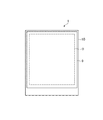
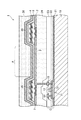
図1は本発明に係る有機EL(electroluminesence)表示装置1の平面図である。図2は有機EL表示装置1の断面図である。 FIG. 1 is a plan view of an organic EL (electroluminescence) display device 1 according to the present invention. FIG. 2 is a cross-sectional view of the organic EL display device 1.
表示装置1には、複数の画素を含む表示領域Dが規定されている。表示領域Dには、複数の色でそれぞれ発光する複数の画素が規定されている。例えば、表示装置1は、複数の画素として、赤画素、緑画素、青画素、及び白画素を含んでいる。画素の色及び色の数はこれに限定されず、適宜変更されてよい。また、画素の配置も特に限定されない。例えば、色の異なる4つの画素が2列及び2行で配置される。また、色の異なる3つ或いは4つの画素は一方向に並んでもよい。 In the display device 1, a display area D including a plurality of pixels is defined. In the display area D, a plurality of pixels that respectively emit light in a plurality of colors are defined. For example, the display device 1 includes a red pixel, a green pixel, a blue pixel, and a white pixel as a plurality of pixels. The color of the pixel and the number of colors are not limited to this, and may be changed as appropriate. Further, the arrangement of the pixels is not particularly limited. For example, four pixels having different colors are arranged in two columns and two rows. Further, three or four pixels having different colors may be arranged in one direction.
表示装置1はTFT基板10を有している。さらに、表示装置1はTFT基板10と対向する対向基板9を有してもよい。TFT基板10の基材10a(図2)は例えばガラスやプラスチックである。図2に示すように、TFT基板10は回路層Cを有している。回路層Cは、後述する有機EL素子へ供給する電流を制御するTFT11を含んでいる。TFT11は複数の画素のそれぞれに形成されている。TFT11は半導体層12とゲート電極13とソース電極14とドレイン電極15とを有している。表示装置1の一例では、半導体層12はゲート絶縁膜21によって覆われる。ゲート電極13はゲート絶縁膜21上に形成され、層間絶縁膜22によって覆われる。ソース電極14とドレイン電極15は層間絶縁膜22上に形成されている。TFT11の構造は図2に示すものに限られず、適宜変更されてよい。回路層Cはパッシベーション膜23によって覆われている。また、図2に示す例では、パッシベーション膜23上に、アクリルなどの樹脂で形成される平坦化膜24が形成されている。
The display device 1 has a
図2に示すように、TFT基板10は陽極2と陽極2と対向する陰極4とを有している。陽極2と陰極4との間に、後述する発光層や電荷輸送層を有する有機層3が形成されている。陽極2は平坦化膜24上に形成される。表示装置1は複数の陽極2を有し、それらは複数の画素にそれぞれ設けられている。陽極2はTFT11のドレイン電極15にコンタクトホールを介して接続している。陰極4は複数の画素に亘って形成されている。すなわち、複数の画素において陰極4は連続している。陰極4上に封止膜26が形成されてもよい。有機EL表示装置1の一例はトップエミッション型である。この場合、陰極4の材料として、例えばITOやIZO、ZnOなどの透明導電性材料を用いることができる。陽極2は、光反射性を有する金属膜、或いはそのような金属膜と透明導電膜との積層膜により構成され、例えばAlNd合金の膜や、ITOとAgとの積層膜、IZOと銀との積層膜を用いることができる。なお、有機EL表示装置1はボトムエミッション型でもよい。この場合、陽極2は透明導電材料によって形成され、陰極4は光を反射する材料を含む。陽極2及び陰極4の材料は上述したものに限定されず、適宜変更されてよい。
As shown in FIG. 2, the
図2に示すように、陽極2上にバンク層25が形成されてもよい。バンク層25は、各画素に、陽極2を露出させる開口(バンク開口)Aを有している。有機層3は陽極2及びバンク層25上に形成され、バンク開口Aの内側において陽極2と接している。一例では、有機層3は複数の画素に亘って形成される。すなわち、複数の画素において有機層3は連続している。この場合、有機層3は例えば白色光を発するように構成され、各画素には、白色光をその画素の色に変換するカラーフィルターが設けられてもよい。他の例では、有機層3は、複数の画素のそれぞれに独立して形成されてもよい。すなわち、各画素に、その画素の色で発光する発光層が形成されてもよい。例えば、赤画素には赤色で発光する発光層が形成され、緑画素には緑色で発光する発光層が形成され、青画素には青色で発光する発光層が形成されてもよい。
As shown in FIG. 2, a
陽極2と有機層3と陰極4とによって有機EL素子が構成されている。図3は素子の積層構造を示す断面図である。本実施形態に係る発光EL素子はマルチフォトンエミッション素子である。すなわち、有機層3は、それぞれが発光層を含み、積層されている複数の発光ユニットを有している。対向する2つの発光ユニットの間に電荷発生層が形成されている。図3の例では、有機層3は第1発光ユニット3Aと第2発光ユニット3Bとを有している。発光ユニット3A,3Bの間に電荷発生層5が形成されている。第1発光ユニット3Aは電荷発生層5に対して陰極4側に形成され、第2発光ユニット3Bは電荷発生層5に対して陽極2側に形成されている。有機層3は2つより多くの発光ユニットを含んでもよい。この場合、有機層3は複数の電荷発生層を有し、各電荷発生層は対向する2つの発光ユニットの間に形成されてもよい。
The
図3に示すように、発光ユニット3A、3Bのそれぞれは発光層3cを有している。発光層3cは、電子と正孔との再結合により発光する層である。複数の発光ユニット3A、3Bを構成する発光層3cの発光色は同じでもよいし、互いに異なっていてもよい。すなわち、複数の発光ユニット3A、3Bを構成する発光層3cの発光材料は同じでもよいし、互いに異なっていてもよい。発光層3cの材料としては、例えば、Alq3(トリス(8-キノリノラト)アルミニウム)などの蛍光発光材料、或いは、「トリス(2−フェニルピリジナト−N,C2’)イリジウム(III)」(Ir(ppy)3)や、「トリス(1−フェニルイソキノリン)イリジウム(III)」(Ir(piq)3)、「ビス[2−(4’,6’−ジフルオロフェニル)ピリジナト−N,C2’]イリジウム(III)ピコリナート」(FIrpic)などの燐光発光材料など、種々の発光材料を用いることができる。発光層3cの材料はこれらに限定されず、適宜変更されてよい。
As shown in FIG. 3, each of the
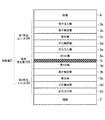
図3に示すように、発光ユニット3A、3Bは、発光層3cの陰極4側に、注入された電子を発光層3cに輸送する電子輸送層3bを有している。電子輸送層3bとしては、例えば、Alq3やBCP(バソクプロイン)を利用することができる。また、発光ユニット3A、3Bは、発光層3cの陽極2側に、注入された正孔を発光層3cに輸送する正孔輸送層3dを有している。正孔輸送層3dとしては、NPB(4,4’−ビス[N−(1−ナフチル)−N−フェニルアミノ]ビフェニル)や、TPD(N,N’−ビス(3−メチルフェニル)−N,N’−ジフェニル−[1,1’−ビフェニル]−4,4’−ジアミン)など公知の材料を用いることができる。さらに、発光ユニット3A、3Bは、正孔輸送層3dの陽極2側に、陽極2或いは後述する電荷発生層5から正孔輸送層3dへの正孔注入障壁を下げる正孔注入層3eを有してもよい。また、第1発光ユニット3Aは、電子輸送層3bの陰極4側に、陰極4から電子輸送層3bへの電子注入障壁を下げる電子注入層3aを有してもよい。これらの各層は、例えば真空蒸着法や、塗布法、印刷法などの方法によって形成され得る。
As shown in FIG. 3, the
図4は有機層3を構成する複数の層のエネルギーレベルの例を示す概略図である。陽極2と陰極4との間に電圧が加えられたとき、陽極2から第2発光ユニット3Bの正孔注入層3eのHOMOに正孔が注入される。正孔は正孔輸送層3dを通って第2発光ユニット3Bの発光層3cのHOMOに移動する。また、陽極2と陰極4との間に電圧が加えられたとき、電荷発生層5から第2発光ユニット3Bの電子輸送層3bのLUMOに電子が注入される。電子は電子輸送層3bのLUMOから発光層3cのLUMOに移動し、発光層3cにおいて正孔と再結合し、励起子を生成する。これにより第2発光ユニット3Bの発光層3cは発光する。同様に、陽極2と陰極4との間に電圧が加えられたとき、陰極4から第1発光ユニット3Aの電子注入層3aのLUMOに電子が注入される。電子は電子輸送層3bを通って発光層3cのLUMOに移動する。また、このとき、電荷発生層5から第1発光ユニット3Aの正孔注入層3eのHOMOに正孔が注入される。正孔は正孔輸送層3dを通って発光層3cのHOMOに移動し、発光層3cにおいて電子と再結合し、励起子を生成する。これにより第1発光ユニット3Aの発光層3cは発光する。
FIG. 4 is a schematic view showing an example of energy levels of a plurality of layers constituting the
図3及び図4に示すように、電荷発生層5は、第1の層5pと、第2の層5nとを含んでいる。図3及び図4の例では、第2の層5nは第1の層5pに対して陽極2側に配置されている。第1の層5pは、電極2,4に電圧が加えられたときに、第1の層5pの陰極4側に配置されている層に正孔を供給し、且つ第1の層5pの陽極2側に配置されている層に電子を供給する層である。図3及び図4の例では、第1の層5pは、第1発光ユニット3Aに正孔を供給し且つ第2の層5nに対して電子を供給する。第2の層5nは第1の層5pから電子を受け取り、第2の層5nの陽極2側に形成されている第2発光ユニット3B(より具体的には、電子輸送層3b)に電子を供給する層である。
As shown in FIGS. 3 and 4, the
第1の層5pの材料としては、例えば酸化バナジウム(V2O5)や酸化モリブデン(MoO3)、酸化レニウム(Re2O7)などの金属酸化物や、例えばテトラフルオロ−テトラシアノ−キノジメタン(F4−TCNQ)やヘキサアザトリフェニレンヘキサカルボニトリル(HATCN6)などの有機材料を用いることができる。
Examples of the material for the
第2の層5nの材料としては、アルカリ金属、アルカリ土類金属、アルカリ金属の酸化物、及びアルカリ土類金属の酸化物のうち少なくとも1つがドープされた電子注入材料を用いることができる。例えば、電子注入材料は、Alq3(トリス(8-キノリノラト)アルミニウム)やBCP(バソクプロイン)などの有機材料に、アルカリ金属、アルカリ土類金属、及び、それらの酸化物のうち少なくとも1つがドープされたされたものを用いることができる。アルカリ金属としてLi,Na,K,Rb,Cs,Frが例示され、またアルカリ土類金属としてBe,Mg,Ca,Sr,Ba,Raが例示される。
As a material of the
電荷発生層5は第1の層5pと第2の層5nとの間に絶縁層5iを有している。後述するように、この絶縁層5iにより、隣接する2つの画素間の混色を防止できる。一例では、絶縁層5iは複数の画素に亘って形成される。すなわち、絶縁層5iは複数の画素において連続して形成される。この場合、絶縁層5iは各画素の発光領域(バンク開口A)にも存在することとなる。したがって、絶縁層5iの材料は透明な絶縁層であることが好ましい。絶縁層5iの材料及び厚さは、第1の層5pで発生した電子がトンネル効果により第2の層5nに移動するように設定される。すなわち、絶縁層5iの材料及び厚さは、第1の層5pから第2の層5nにトンネル電流が流れるように設定されている。絶縁層5iの材料としては、透明な絶縁材料、例えば、酸化シリコンや、窒化シリコンを利用することができる。絶縁層5iの厚さは、例えば、数ナノメートルである。第1の層5p、第2の層5n、及び絶縁層5iは、例えば,化学蒸着(CVD)法により形成できる。
The
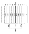
図5は電荷発生層5の動作機構を説明するための図である。図5(a)は絶縁層5iを有している電荷発生層5が示されている。図5(b)では、上述した第1の層5pと第2の層5nとを有しているものの、絶縁層5iを有していない電荷発生層5Sが示されている。
FIG. 5 is a diagram for explaining the operation mechanism of the
図5(b)に示すように、電荷発生層5Sには絶縁層5iが設けられていない。そのため、第2の層5nがドーパントとして含んでいるアルカリ金属、アルカリ土類金属、或いはそれらの酸化物が、第1の層5pに拡散してしまい、その結果、第1の層5pの界面近くで電気抵抗率が下がる。第2の層5nのLUMOのエネルギーレベルは第1の層5pのLUMOのエネルギーレベルよりも高いので、図中矢印で示すように第1の層5pで発生した電子は第1の層5pの界面に蓄積する。電荷発生層5Sでは、第1の層5pの界面近くで電気抵抗率が下がっているので、第1の層5pと第2の層5nとの間のエネルギー障壁を越える前に第1の層5pの界面に沿って隣の画素に流れる。その結果、隣り合う2つの画素での混色が生じ易くなる。
As shown in FIG. 5B, the charge generation layer 5S is not provided with the insulating
一方、本実施形態の電荷発生層5は、図5(a)に示すように、絶縁層5iを有している。そのため、第2の層5nのドーパントが第1の層5pに拡散することを防ぐことができ、その結果、第1の層5pの界面近くでの電気抵抗率の低下を抑えることができる。このため、第1の層5pで発生した電子が第1の層5pの界面に沿って流れることを抑えることができるので、隣り合う2つの画素での混色を抑えることができる。第1の層5pで発生した電子はトンネル効果により第2の層5nに移動する。
On the other hand, the
絶縁層5iの材料としては、無機材料を用いることが好ましい。無機材料では一般的に原子間隔が小さい。そのため、無機材料を利用することにより、第2の層5nのドーパントが第1の層5pに拡散することを効果的に抑えることができる。
As a material for the insulating
絶縁層5iは、好ましくは、第2の層5nのドーパントが第2の層5nから第1の層5pの界面に拡散した場合における第1の層5pよりも高い電気抵抗率を有する。すなわち、絶縁層5iは、好ましくは、図5(b)で示される第1の層5pにおける第2の層5n側の部分よりも高い電気抵抗率を有する。絶縁層5iとしてこのような材料を用いることにより、隣の画素に向かう電子の流れを効果的に抑えることができる。絶縁層5iは、より好ましくは、第1の層5pを構成する材料よりも高い電気抵抗率を有する。こうすることにより、隣の画素に向かう電子の流れをさらに効果的に抑えることができる。絶縁層5iの材料としては、上述したように、例えば酸化シリコンや窒化シリコンなどを利用することができる。なお、第1の層5pに沿った方向への電子の流れが生じない程度に第1の層5p自体の電気抵抗率(ドーパントが拡散していない状態での電気抵抗率)が高く、且つ、絶縁層5iがドーパントの第1の層5pへの拡散を抑えている場合には、絶縁層5iの電気抵抗率は必ずしも上述したものに限定されない。
The insulating
絶縁層5iは必ずしも複数の画素に亘って形成されていなくてもよい。すなわち、各画素は、絶縁層5iが形成されている領域と、絶縁層5iが形成されていない領域とを含んでもよい。図6は、このような形態の電荷発生層5を示す図である。この図に示されるように、各画素は、その発光領域(図2で示したバンク開口Aの領域)に、絶縁層5iが形成され且つ互いに離れて位置している複数の領域を有してもよい。すなわち、絶縁層5iは、発光領域において分散して形成されてもよい。このような電荷発生層5によれば、絶縁層5iが形成されていない領域では、トンネル効果によることなく第1の層5pから第2の層5nに電子を移動させることができ、絶縁層5iが形成されている領域では、第1の層5pから第2の層5nにトンネル効果によって電子を移動させることができる。また、絶縁層5iにより、電子が第1の層5pの界面に沿って流れることを抑えることができる。
The insulating
また、絶縁層5iは隣接する2つの画素の間にだけ形成されてもよい。すなわち、絶縁層5iは、バンク層25が形成されているために発光しない領域、すなわち発光領域を取り囲む領域にだけ絶縁層5iを有し、絶縁層5iは発光領域には形成されなくてもよい。こうすることにより、絶縁層5iが形成されていない領域で、トンネル効果によることなく第1の層5pから第2の層5nに電子を移動させることができる。
Further, the insulating
図7は電荷発生層5のさらに別の変形例を示す図である。この図では、電荷発生層5に替えて電荷発生層105を有する有機EL素子が示されている。この図では、これまで説明した箇所と同一箇所には同一符合を付している。
FIG. 7 is a view showing still another modified example of the
電荷発生層105は第1発光ユニット3Aと第2発光ユニット3Bとの間に形成されている。電荷発生層105は、上述の第1の層5pと第2の層5nとを有している。電荷発生層105では、電荷発生層5とは異なり、第2の層5nは、第1の層5pに対して陰極4側に形成されている。したがって、図7の例では、第1の層5pは、第2発光ユニット3B(より具体的には、電子輸送層3b)に電子を供給する。また、後において詳説するように、第2の層5nは第1の層5pから正孔を受け取り、第2の層5nの陰極4側に形成されている第1発光ユニット3A(より具体的には、正孔注入層3e)に電子を供給する。第1の層5pの材料は、図3及び図5(a)で示す第1の層5pと同様、例えばV2O5やMoO3、Re2O7などの金属酸化物や、F4−TCNQやHATCN6などの有機材料などを用いることができる。第2の層5nの材料は、図3及び図5(a)で示す第2の層5nと同様、例えば、Alq3やBCPなどの有機材料にアルカリ金属、アルカリ土類金属或いはそれらの酸化物がドープされた電子注入材料を用いることができる。
The charge generation layer 105 is formed between the first
また、電荷発生層105は、第1の層5pと第2の層5nとの間に、絶縁層5iを有している。絶縁層5iの材料は、電荷発生層5で使用される絶縁層5iと同じものを利用できる。すなわち、電荷発生層105の絶縁層5iは、ドーパントが第2の層5nから第1の層5pに拡散した場合における第1の層5pよりも高い電気抵抗率を有する。絶縁層5iの材料としては、上述したように、例えば酸化シリコンや窒化シリコンを利用することができる。絶縁層5iによって、第2の層5nのドーパントが第1の層5pに拡散することを防ぐことができる。
The charge generation layer 105 has an
電荷発生層105を有する形態では、アヴァランシェ機構を利用して、第1の層5pから第2の層5nに電荷を供給できる。図8は電荷発生層105の動作機構を説明するための図である。
In the embodiment having the charge generation layer 105, charges can be supplied from the
陽極2と陰極4との間に電圧が加えられたとき、第1の層5pのHOMOとLUMOとに正孔と電子とがそれぞれ発生する。電子は、第1の層5pの陽極2側に形成されている層、具体的には第2発光ユニット3Bに移動し、第1の層5pで発生した正孔は絶縁層5iに向けて移動する。陽極2と陰極4との間に加えられる電圧が高い場合、第1の層5pで発生した正孔は、第1の層5p及び/又は絶縁層5iを通る過程で衝突電離を生じ得る(アヴァランシェ降伏)。また、陽極2と陰極4との間に加えられる電圧が高い場合、第1の層5pで発生した電子は、第1の層5pを通る過程で衝突電離を生じ得る(アヴァランシェ降伏)。衝突電離により発生した電子は陽極2に向けて移動し、衝突電離により発生した正孔は第2の層5nに移動する。図7及び8で示す形態においても、第1の層5pと第2の層5nとの間に絶縁層5iが形成されているので、電荷が第1の層5pの界面に沿って移動することを防ぐことができる。なお、陽極2と陰極4との間に加えられる電圧が高いために、第2の層5nにおいて衝突電離(アヴァランシェ降伏)が生じる可能性がある。この場合、衝突電離により第2の層5nに発生した電子は陽極2に向けて移動し、トンネル効果により絶縁層5iを通過し、第1の層5pに移動する。一方、衝突電離により第2の層5nに発生した正孔は陰極4に向けて移動し、第1発光ユニット3A(より具体的には、第1発光ユニット3Aの正孔注入層3e)に移動する。
When a voltage is applied between the
本発明は、上述した実施形態に限定されるものではなく種々の変形が可能である。実施形態で説明した構成は、実質的に同一の構成、同一の作用効果を奏する構成又は同一の目的を達成することができる構成で置き換えることができる。 The present invention is not limited to the above-described embodiments, and various modifications can be made. The configurations described in the embodiments can be replaced with substantially the same configurations, configurations that exhibit the same operational effects, or configurations that can achieve the same purpose.
例えば、図2において、陰極4が平坦化膜24上に形成され、陽極2が有機層3上に形成されてもよい。
For example, in FIG. 2, the cathode 4 may be formed on the
1 有機EL表示装置、2 陽極、3 有機層、3A,3B 発光ユニット、3a 電子注入層、3b 電子輸送層、3c 発光層、3d 正孔輸送層、3e 正孔注入層、4 陰極、5 電荷発生層、5i 絶縁層、5p 第1の層、5n 第2の層、105 電荷発生層。 1 organic EL display device, 2 anode, 3 organic layers, 3A, 3B light emitting unit, 3a electron injection layer, 3b electron transport layer, 3c light emission layer, 3d hole transport layer, 3e hole injection layer, 4 cathode, 5 charge Generation layer, 5i insulating layer, 5p first layer, 5n second layer, 105 charge generation layer.
Claims (13)
前記複数の画素に形成されている陰極と、
前記陰極に対向している陽極と、
前記陰極と前記陽極との間で積層され、それぞれが発光層を含んでいる少なくとも2つの発光ユニットと、
前記少なくとも2つの発光ユニットの間に形成されている電荷発生層と、を備え、
前記電荷発生層は、前記少なくとも2つの発光ユニットのうちの一方の発光ユニットに電子と正孔のうちの一方の電荷を供給する第1の層と、他方の電荷を前記第1の層から受け取り、他方の発光ユニットに前記他方の電荷を供給する第2の層と、を有し、
前記複数の画素のうち少なくとも1つの画素の前記電荷発生層は、前記第1の層と前記第2の層との間に形成されている絶縁層を含んでいる
ことを特徴とする有機EL表示装置。 A plurality of pixels;
A cathode formed on the plurality of pixels;
An anode facing the cathode;
At least two light emitting units stacked between the cathode and the anode, each including a light emitting layer;
A charge generation layer formed between the at least two light emitting units,
The charge generation layer receives from the first layer a first layer that supplies one charge of electrons and holes to one light emitting unit of the at least two light emitting units, and the other charge from the first layer. A second layer for supplying the other light-emitting unit with the other charge,
The organic EL display, wherein the charge generation layer of at least one of the plurality of pixels includes an insulating layer formed between the first layer and the second layer. apparatus.
ことを特徴とする請求項1に記載の有機EL表示装置。 The second layer includes at least one of an alkali metal, an alkaline earth metal, an alkali metal oxide, and an alkaline earth metal oxide as a dopant. Organic EL display device.
ことを特徴とする請求項2に記載の有機EL表示装置。 The insulating layer has an electric resistivity higher than that of the first layer when the dopant diffuses from the second layer to the interface of the first layer. The organic EL display device described.
ことを特徴とする請求項1に記載の有機EL表示装置。 The organic EL display device according to claim 1, wherein the insulating layer is formed of a material having a higher electrical resistivity than the first layer.
ことを特徴とする請求項1に記載の有機EL表示装置。 The organic EL display device according to claim 1, wherein the insulating layer is formed of an inorganic material.
ことを特徴とする請求項5に記載の有機EL表示装置。 The organic EL display device according to claim 5, wherein the insulating layer includes at least one of silicon oxide and silicon nitride.
ことを特徴とする請求項1に記載の有機EL表示装置。 The insulating layer has a thickness that causes charge transfer due to a tunnel effect from the first layer to the second layer when a voltage is applied between the cathode and the anode. The organic EL display device according to claim 1.
ことを特徴とする請求項1に記載の有機EL表示装置。 The organic EL display device according to claim 1, wherein the first layer is a layer that is positioned on the cathode side with respect to the second layer and supplies electrons to the second layer. .
ことを特徴とする請求項1に記載の有機EL表示装置。 The organic EL display according to claim 1, wherein the first layer is a layer that is located on the anode side with respect to the second layer and supplies holes to the second layer. apparatus.
ことを特徴とする請求項9に記載の有機EL表示装置。 10. The organic EL according to claim 9, wherein when a voltage is applied between the cathode and the anode, charges move from the first layer to the second layer by avalanche breakdown. Display device.
ことを特徴とする請求項1に記載の有機EL表示装置。 The organic EL display device according to claim 1, wherein the at least one pixel includes a region where the insulating layer is formed and a region where the insulating layer is not formed.
ことを特徴とする請求項11に記載の有機EL表示装置。 The organic EL display device according to claim 11, wherein the at least one pixel includes a plurality of regions in which the insulating layer is formed and are spaced apart from each other.
ことを特徴とする請求項1に記載の有機EL表示装置。 The organic EL display device according to claim 1, wherein the insulating layer is formed in a light emitting region of the at least one pixel.
Priority Applications (1)
| Application Number | Priority Date | Filing Date | Title |
|---|---|---|---|
| JP2015128875A JP2017016739A (en) | 2015-06-26 | 2015-06-26 | Organic EL display device |
Applications Claiming Priority (1)
| Application Number | Priority Date | Filing Date | Title |
|---|---|---|---|
| JP2015128875A JP2017016739A (en) | 2015-06-26 | 2015-06-26 | Organic EL display device |
Publications (1)
| Publication Number | Publication Date |
|---|---|
| JP2017016739A true JP2017016739A (en) | 2017-01-19 |
Family
ID=57830841
Family Applications (1)
| Application Number | Title | Priority Date | Filing Date |
|---|---|---|---|
| JP2015128875A Pending JP2017016739A (en) | 2015-06-26 | 2015-06-26 | Organic EL display device |
Country Status (1)
| Country | Link |
|---|---|
| JP (1) | JP2017016739A (en) |
Cited By (1)
| Publication number | Priority date | Publication date | Assignee | Title |
|---|---|---|---|---|
| CN107611271A (en) * | 2017-08-10 | 2018-01-19 | 上海天马有机发光显示技术有限公司 | Organic light emitting diode, display panel and display device |
-
2015
- 2015-06-26 JP JP2015128875A patent/JP2017016739A/en active Pending
Cited By (1)
| Publication number | Priority date | Publication date | Assignee | Title |
|---|---|---|---|---|
| CN107611271A (en) * | 2017-08-10 | 2018-01-19 | 上海天马有机发光显示技术有限公司 | Organic light emitting diode, display panel and display device |
Similar Documents
| Publication | Publication Date | Title |
|---|---|---|
| US9118032B2 (en) | Organic light emitting device | |
| US9406908B2 (en) | Organic light emitting device | |
| US10418580B2 (en) | Organic electroluminescent device and organic electroluminescent display device | |
| KR101429537B1 (en) | Organic light emitting diodes | |
| KR20170113780A (en) | Organic light emitting display device and method of manufacturing the organic light emitting display device | |
| EP3276698B1 (en) | Organic light emitting device and organic light emitting display using the same | |
| US9299950B2 (en) | Organic light emitting display apparatus | |
| KR102146367B1 (en) | Organic light emitting diode device | |
| KR102422769B1 (en) | Organic light emitting display apparatus | |
| US8878171B2 (en) | Organic light emitting display device | |
| KR102574052B1 (en) | Organic light emitting display device | |
| KR101374891B1 (en) | Display device | |
| US9692002B2 (en) | Organic light emitting display device | |
| JP5992495B2 (en) | Organic light emitting diode and organic light emitting diode display device | |
| KR102596337B1 (en) | Organic light emitting display device | |
| KR20100036055A (en) | Organic light emitting display | |
| JP2017016739A (en) | Organic EL display device | |
| US9210764B2 (en) | Organic light emitting diode device and method of manufacturing the same | |
| KR102567321B1 (en) | White organic light emitting diode and display device using the same | |
| KR102410031B1 (en) | Organic light emitting diode, manufacturing method for the same, and organic light emitting display device having the organic light emitting diode | |
| KR102435038B1 (en) | Organic light emitting display device | |
| KR20150041314A (en) | Organic Electroluminescence Device and fabrication method thereof | |
| KR20190057749A (en) | Organic light emitting display device and method for manufacturing the same | |
| EP4207968A1 (en) | Light-emitting device and light-emitting display device including the same | |
| KR20170074468A (en) | Organic light emitting display device |