EP3125029A2 - Display panel having substrate including thin film transistor - Google Patents
Display panel having substrate including thin film transistor Download PDFInfo
- Publication number
- EP3125029A2 EP3125029A2 EP16181826.5A EP16181826A EP3125029A2 EP 3125029 A2 EP3125029 A2 EP 3125029A2 EP 16181826 A EP16181826 A EP 16181826A EP 3125029 A2 EP3125029 A2 EP 3125029A2
- Authority
- EP
- European Patent Office
- Prior art keywords
- display panel
- stopper layers
- panel according
- substrate
- touch sensing
- Prior art date
- Legal status (The legal status is an assumption and is not a legal conclusion. Google has not performed a legal analysis and makes no representation as to the accuracy of the status listed.)
- Granted
Links
Images



Classifications
-
- G—PHYSICS
- G02—OPTICS
- G02F—OPTICAL DEVICES OR ARRANGEMENTS FOR THE CONTROL OF LIGHT BY MODIFICATION OF THE OPTICAL PROPERTIES OF THE MEDIA OF THE ELEMENTS INVOLVED THEREIN; NON-LINEAR OPTICS; FREQUENCY-CHANGING OF LIGHT; OPTICAL LOGIC ELEMENTS; OPTICAL ANALOGUE/DIGITAL CONVERTERS
- G02F1/00—Devices or arrangements for the control of the intensity, colour, phase, polarisation or direction of light arriving from an independent light source, e.g. switching, gating or modulating; Non-linear optics
- G02F1/01—Devices or arrangements for the control of the intensity, colour, phase, polarisation or direction of light arriving from an independent light source, e.g. switching, gating or modulating; Non-linear optics for the control of the intensity, phase, polarisation or colour
- G02F1/13—Devices or arrangements for the control of the intensity, colour, phase, polarisation or direction of light arriving from an independent light source, e.g. switching, gating or modulating; Non-linear optics for the control of the intensity, phase, polarisation or colour based on liquid crystals, e.g. single liquid crystal display cells
- G02F1/133—Constructional arrangements; Operation of liquid crystal cells; Circuit arrangements
- G02F1/136—Liquid crystal cells structurally associated with a semi-conducting layer or substrate, e.g. cells forming part of an integrated circuit
- G02F1/1362—Active matrix addressed cells
- G02F1/136286—Wiring, e.g. gate line, drain line
-
- G—PHYSICS
- G06—COMPUTING OR CALCULATING; COUNTING
- G06F—ELECTRIC DIGITAL DATA PROCESSING
- G06F3/00—Input arrangements for transferring data to be processed into a form capable of being handled by the computer; Output arrangements for transferring data from processing unit to output unit, e.g. interface arrangements
- G06F3/01—Input arrangements or combined input and output arrangements for interaction between user and computer
- G06F3/03—Arrangements for converting the position or the displacement of a member into a coded form
- G06F3/041—Digitisers, e.g. for touch screens or touch pads, characterised by the transducing means
- G06F3/0412—Digitisers structurally integrated in a display
-
- G—PHYSICS
- G02—OPTICS
- G02F—OPTICAL DEVICES OR ARRANGEMENTS FOR THE CONTROL OF LIGHT BY MODIFICATION OF THE OPTICAL PROPERTIES OF THE MEDIA OF THE ELEMENTS INVOLVED THEREIN; NON-LINEAR OPTICS; FREQUENCY-CHANGING OF LIGHT; OPTICAL LOGIC ELEMENTS; OPTICAL ANALOGUE/DIGITAL CONVERTERS
- G02F1/00—Devices or arrangements for the control of the intensity, colour, phase, polarisation or direction of light arriving from an independent light source, e.g. switching, gating or modulating; Non-linear optics
- G02F1/01—Devices or arrangements for the control of the intensity, colour, phase, polarisation or direction of light arriving from an independent light source, e.g. switching, gating or modulating; Non-linear optics for the control of the intensity, phase, polarisation or colour
- G02F1/13—Devices or arrangements for the control of the intensity, colour, phase, polarisation or direction of light arriving from an independent light source, e.g. switching, gating or modulating; Non-linear optics for the control of the intensity, phase, polarisation or colour based on liquid crystals, e.g. single liquid crystal display cells
- G02F1/133—Constructional arrangements; Operation of liquid crystal cells; Circuit arrangements
- G02F1/1333—Constructional arrangements; Manufacturing methods
- G02F1/13338—Input devices, e.g. touch panels
-
- G—PHYSICS
- G02—OPTICS
- G02F—OPTICAL DEVICES OR ARRANGEMENTS FOR THE CONTROL OF LIGHT BY MODIFICATION OF THE OPTICAL PROPERTIES OF THE MEDIA OF THE ELEMENTS INVOLVED THEREIN; NON-LINEAR OPTICS; FREQUENCY-CHANGING OF LIGHT; OPTICAL LOGIC ELEMENTS; OPTICAL ANALOGUE/DIGITAL CONVERTERS
- G02F1/00—Devices or arrangements for the control of the intensity, colour, phase, polarisation or direction of light arriving from an independent light source, e.g. switching, gating or modulating; Non-linear optics
- G02F1/01—Devices or arrangements for the control of the intensity, colour, phase, polarisation or direction of light arriving from an independent light source, e.g. switching, gating or modulating; Non-linear optics for the control of the intensity, phase, polarisation or colour
- G02F1/13—Devices or arrangements for the control of the intensity, colour, phase, polarisation or direction of light arriving from an independent light source, e.g. switching, gating or modulating; Non-linear optics for the control of the intensity, phase, polarisation or colour based on liquid crystals, e.g. single liquid crystal display cells
- G02F1/133—Constructional arrangements; Operation of liquid crystal cells; Circuit arrangements
- G02F1/1333—Constructional arrangements; Manufacturing methods
- G02F1/1339—Gaskets; Spacers; Sealing of cells
- G02F1/13394—Gaskets; Spacers; Sealing of cells spacers regularly patterned on the cell subtrate, e.g. walls, pillars
-
- G—PHYSICS
- G02—OPTICS
- G02F—OPTICAL DEVICES OR ARRANGEMENTS FOR THE CONTROL OF LIGHT BY MODIFICATION OF THE OPTICAL PROPERTIES OF THE MEDIA OF THE ELEMENTS INVOLVED THEREIN; NON-LINEAR OPTICS; FREQUENCY-CHANGING OF LIGHT; OPTICAL LOGIC ELEMENTS; OPTICAL ANALOGUE/DIGITAL CONVERTERS
- G02F1/00—Devices or arrangements for the control of the intensity, colour, phase, polarisation or direction of light arriving from an independent light source, e.g. switching, gating or modulating; Non-linear optics
- G02F1/01—Devices or arrangements for the control of the intensity, colour, phase, polarisation or direction of light arriving from an independent light source, e.g. switching, gating or modulating; Non-linear optics for the control of the intensity, phase, polarisation or colour
- G02F1/13—Devices or arrangements for the control of the intensity, colour, phase, polarisation or direction of light arriving from an independent light source, e.g. switching, gating or modulating; Non-linear optics for the control of the intensity, phase, polarisation or colour based on liquid crystals, e.g. single liquid crystal display cells
- G02F1/133—Constructional arrangements; Operation of liquid crystal cells; Circuit arrangements
- G02F1/136—Liquid crystal cells structurally associated with a semi-conducting layer or substrate, e.g. cells forming part of an integrated circuit
- G02F1/1362—Active matrix addressed cells
- G02F1/1368—Active matrix addressed cells in which the switching element is a three-electrode device
-
- G—PHYSICS
- G06—COMPUTING OR CALCULATING; COUNTING
- G06F—ELECTRIC DIGITAL DATA PROCESSING
- G06F3/00—Input arrangements for transferring data to be processed into a form capable of being handled by the computer; Output arrangements for transferring data from processing unit to output unit, e.g. interface arrangements
- G06F3/01—Input arrangements or combined input and output arrangements for interaction between user and computer
- G06F3/03—Arrangements for converting the position or the displacement of a member into a coded form
- G06F3/041—Digitisers, e.g. for touch screens or touch pads, characterised by the transducing means
- G06F3/0416—Control or interface arrangements specially adapted for digitisers
- G06F3/04164—Connections between sensors and controllers, e.g. routing lines between electrodes and connection pads
-
- G—PHYSICS
- G06—COMPUTING OR CALCULATING; COUNTING
- G06F—ELECTRIC DIGITAL DATA PROCESSING
- G06F3/00—Input arrangements for transferring data to be processed into a form capable of being handled by the computer; Output arrangements for transferring data from processing unit to output unit, e.g. interface arrangements
- G06F3/01—Input arrangements or combined input and output arrangements for interaction between user and computer
- G06F3/03—Arrangements for converting the position or the displacement of a member into a coded form
- G06F3/041—Digitisers, e.g. for touch screens or touch pads, characterised by the transducing means
- G06F3/044—Digitisers, e.g. for touch screens or touch pads, characterised by the transducing means by capacitive means
-
- G—PHYSICS
- G06—COMPUTING OR CALCULATING; COUNTING
- G06F—ELECTRIC DIGITAL DATA PROCESSING
- G06F3/00—Input arrangements for transferring data to be processed into a form capable of being handled by the computer; Output arrangements for transferring data from processing unit to output unit, e.g. interface arrangements
- G06F3/01—Input arrangements or combined input and output arrangements for interaction between user and computer
- G06F3/03—Arrangements for converting the position or the displacement of a member into a coded form
- G06F3/041—Digitisers, e.g. for touch screens or touch pads, characterised by the transducing means
- G06F3/044—Digitisers, e.g. for touch screens or touch pads, characterised by the transducing means by capacitive means
- G06F3/0443—Digitisers, e.g. for touch screens or touch pads, characterised by the transducing means by capacitive means using a single layer of sensing electrodes
-
- H—ELECTRICITY
- H10—SEMICONDUCTOR DEVICES; ELECTRIC SOLID-STATE DEVICES NOT OTHERWISE PROVIDED FOR
- H10D—INORGANIC ELECTRIC SEMICONDUCTOR DEVICES
- H10D86/00—Integrated devices formed in or on insulating or conducting substrates, e.g. formed in silicon-on-insulator [SOI] substrates or on stainless steel or glass substrates
- H10D86/40—Integrated devices formed in or on insulating or conducting substrates, e.g. formed in silicon-on-insulator [SOI] substrates or on stainless steel or glass substrates characterised by multiple TFTs
- H10D86/441—Interconnections, e.g. scanning lines
-
- H—ELECTRICITY
- H10—SEMICONDUCTOR DEVICES; ELECTRIC SOLID-STATE DEVICES NOT OTHERWISE PROVIDED FOR
- H10D—INORGANIC ELECTRIC SEMICONDUCTOR DEVICES
- H10D86/00—Integrated devices formed in or on insulating or conducting substrates, e.g. formed in silicon-on-insulator [SOI] substrates or on stainless steel or glass substrates
- H10D86/40—Integrated devices formed in or on insulating or conducting substrates, e.g. formed in silicon-on-insulator [SOI] substrates or on stainless steel or glass substrates characterised by multiple TFTs
- H10D86/60—Integrated devices formed in or on insulating or conducting substrates, e.g. formed in silicon-on-insulator [SOI] substrates or on stainless steel or glass substrates characterised by multiple TFTs wherein the TFTs are in active matrices
-
- G—PHYSICS
- G02—OPTICS
- G02F—OPTICAL DEVICES OR ARRANGEMENTS FOR THE CONTROL OF LIGHT BY MODIFICATION OF THE OPTICAL PROPERTIES OF THE MEDIA OF THE ELEMENTS INVOLVED THEREIN; NON-LINEAR OPTICS; FREQUENCY-CHANGING OF LIGHT; OPTICAL LOGIC ELEMENTS; OPTICAL ANALOGUE/DIGITAL CONVERTERS
- G02F1/00—Devices or arrangements for the control of the intensity, colour, phase, polarisation or direction of light arriving from an independent light source, e.g. switching, gating or modulating; Non-linear optics
- G02F1/01—Devices or arrangements for the control of the intensity, colour, phase, polarisation or direction of light arriving from an independent light source, e.g. switching, gating or modulating; Non-linear optics for the control of the intensity, phase, polarisation or colour
- G02F1/13—Devices or arrangements for the control of the intensity, colour, phase, polarisation or direction of light arriving from an independent light source, e.g. switching, gating or modulating; Non-linear optics for the control of the intensity, phase, polarisation or colour based on liquid crystals, e.g. single liquid crystal display cells
- G02F1/133—Constructional arrangements; Operation of liquid crystal cells; Circuit arrangements
- G02F1/1333—Constructional arrangements; Manufacturing methods
- G02F1/1335—Structural association of cells with optical devices, e.g. polarisers or reflectors
- G02F1/133509—Filters, e.g. light shielding masks
- G02F1/133512—Light shielding layers, e.g. black matrix
-
- G—PHYSICS
- G02—OPTICS
- G02F—OPTICAL DEVICES OR ARRANGEMENTS FOR THE CONTROL OF LIGHT BY MODIFICATION OF THE OPTICAL PROPERTIES OF THE MEDIA OF THE ELEMENTS INVOLVED THEREIN; NON-LINEAR OPTICS; FREQUENCY-CHANGING OF LIGHT; OPTICAL LOGIC ELEMENTS; OPTICAL ANALOGUE/DIGITAL CONVERTERS
- G02F1/00—Devices or arrangements for the control of the intensity, colour, phase, polarisation or direction of light arriving from an independent light source, e.g. switching, gating or modulating; Non-linear optics
- G02F1/01—Devices or arrangements for the control of the intensity, colour, phase, polarisation or direction of light arriving from an independent light source, e.g. switching, gating or modulating; Non-linear optics for the control of the intensity, phase, polarisation or colour
- G02F1/13—Devices or arrangements for the control of the intensity, colour, phase, polarisation or direction of light arriving from an independent light source, e.g. switching, gating or modulating; Non-linear optics for the control of the intensity, phase, polarisation or colour based on liquid crystals, e.g. single liquid crystal display cells
- G02F1/133—Constructional arrangements; Operation of liquid crystal cells; Circuit arrangements
- G02F1/1333—Constructional arrangements; Manufacturing methods
- G02F1/1337—Surface-induced orientation of the liquid crystal molecules, e.g. by alignment layers
-
- G—PHYSICS
- G02—OPTICS
- G02F—OPTICAL DEVICES OR ARRANGEMENTS FOR THE CONTROL OF LIGHT BY MODIFICATION OF THE OPTICAL PROPERTIES OF THE MEDIA OF THE ELEMENTS INVOLVED THEREIN; NON-LINEAR OPTICS; FREQUENCY-CHANGING OF LIGHT; OPTICAL LOGIC ELEMENTS; OPTICAL ANALOGUE/DIGITAL CONVERTERS
- G02F1/00—Devices or arrangements for the control of the intensity, colour, phase, polarisation or direction of light arriving from an independent light source, e.g. switching, gating or modulating; Non-linear optics
- G02F1/01—Devices or arrangements for the control of the intensity, colour, phase, polarisation or direction of light arriving from an independent light source, e.g. switching, gating or modulating; Non-linear optics for the control of the intensity, phase, polarisation or colour
- G02F1/13—Devices or arrangements for the control of the intensity, colour, phase, polarisation or direction of light arriving from an independent light source, e.g. switching, gating or modulating; Non-linear optics for the control of the intensity, phase, polarisation or colour based on liquid crystals, e.g. single liquid crystal display cells
- G02F1/133—Constructional arrangements; Operation of liquid crystal cells; Circuit arrangements
- G02F1/1333—Constructional arrangements; Manufacturing methods
- G02F1/1339—Gaskets; Spacers; Sealing of cells
- G02F1/13396—Spacers having different sizes
-
- G—PHYSICS
- G02—OPTICS
- G02F—OPTICAL DEVICES OR ARRANGEMENTS FOR THE CONTROL OF LIGHT BY MODIFICATION OF THE OPTICAL PROPERTIES OF THE MEDIA OF THE ELEMENTS INVOLVED THEREIN; NON-LINEAR OPTICS; FREQUENCY-CHANGING OF LIGHT; OPTICAL LOGIC ELEMENTS; OPTICAL ANALOGUE/DIGITAL CONVERTERS
- G02F2201/00—Constructional arrangements not provided for in groups G02F1/00 - G02F7/00
- G02F2201/40—Arrangements for improving the aperture ratio
Definitions
- the present invention relates to a substrate including a thin film transistor and a display panel having the same, and more particularly, to a substrate including a thin film transistor, which may prevent light leakage without a reduction in an aperture ratio, and to a display panel having the same.
- An image display which displays various information on a screen, is a core technology of the information communication era and is being developed to achieve thinner, lighter, more portable and better-performing products. Accordingly, flat panel displays, which may overcome the disadvantage of the weight and volume of cathode ray tubes (CRT), are in the spotlight.
- CTR cathode ray tubes
- a liquid crystal display displays an image by adjusting the light transmittance of liquid crystals via an electric field, which is formed between a common electrode and a pixel electrode connected to a thin film transistor.
- the liquid crystal display is formed such that a substrate including a color filter and a substrate including a thin film transistor are bonded to each other with a liquid crystal layer interposed therebetween.
- a column spacer is formed between the thin film transistor substrate and the color filter substrate in order to maintain a cell gap.
- the column spacer When pressure is applied from outside the liquid crystal display, the column spacer is moved by the pressure. The movement of the column spacer causes damage to an alignment film, which is in contact with the column spacer. Because the damaged alignment film cannot align liquid crystals in a desired direction, light leakage occurs in the damaged region of the alignment film, which is problematic.
- the substrate when the substrate is reduced in thickness to achieve a thinner liquid crystal display, the substrate having a reduced thickness is easily deformed even by small pressure, whereby light leakage from the thin liquid crystal display is increased somewhat.
- the line width of a black matrix around the column spacer may be increased in order to solve this light leakage problem, this decreases an aperture ratio.
- the present invention is directed to a substrate including a thin film transistor and a display panel having the same that substantially obviate one or more problems due to limitations and disadvantages of the related art.
- An object of the present invention is to provide a substrate including a thin film transistor, which may prevent light leakage without a reduction in an aperture ratio, and a display panel having the same.
- a plurality of stopper layers is spaced apart from each other with a space interposed therebetween and is located on the same plane as a touch sensing line, and a column spacer is located to overlap the space between the stopper layers.
- a display panel comprises a common electrode located on a lower substrate for receiving a user touch signal; a touch sensing line connected to the common electrode; a plurality of first stopper layers located on a same plane as the touch sensing line and spaced apart from each other with a space therebetween; and a column spacer located on an upper substrate opposite to the lower substrate, to overlap the space between the first stopper layers.
- first to third sub-pixel areas that create different colors may be defined on the upper and/or lower substrate.
- the display panel may further comprise a black matrix located on the upper substrate for defining the first to third sub-pixel areas that create different colors.
- a color filter located in the first to third sub-pixel areas is further provided.
- the touch sensing line may be located to overlap the black matrix between the first and second sub-pixel areas.
- Each first stopper layer may be located to overlap the black matrix between the first and third sub-pixel areas.
- the display panel may further comprise a second stopper layer located to overlap the black matrix between the second and third sub-pixel areas.
- the second stopper layer may be formed of a same material on the same plane with the touch sensing line.
- the display panel may further comprise a gate line on the lower substrate and a data line located to cross the gate line to define first to third sub-pixel areas.
- the touch sensing line may be located to overlap the data line located between the first and second sub-pixel areas.
- Each first stopper layer may be located to overlap the data line located between the first and third sub-pixel areas.
- a second stopper layer may be located to overlap the data line located between the second and third sub-pixel areas.
- the second stopper layer may be formed of a same material on the same plane as the touch sensing line.
- Each first stopper layer may be spaced apart from an adjacent first stopper layer in a region of the black matrix that overlaps an intersection of the data line and the gate line located between the first and third sub-pixel areas.
- Each second stopper layer may be spaced apart from an adjacent second stopper layer in a region of the black matrix that overlaps an intersection of the data line and the gate line located between the second and third sub-pixel areas.
- a thin film transistor substrate is provided, the thin film transistor substrate being located opposite a substrate including a color filter with a column spacer interposed therebetween, and the thin film transistor substrate comprising: a plurality of first stopper layers spaced apart from each other with a space therebetween, the space being located in a region overlapping the column spacer; a touch sensing line located on a same plane as the first stopper layers; and a common electrode connected to the touch sensing line for receiving a user touch signal.
- the thin film transistor substrate may further comprise a plurality of second stopper layers overlapping the data line that does not overlap the touch sensing line.
- the first and second stopper layers may be formed of a same material on the same plane as the touch sensing line.
- FIG. 1 is a block diagram illustrating an in-cell touch type display in accordance with one or more embodiments of the present invention. All the components of the in-cell touch type display according to all embodiments of the present invention are operatively coupled and configured.
- the touch display illustrated in FIG. 1 includes a data driver 194, a gate driver 192, a touch driver 196, and a display panel.
- the data driver 194 converts digital data from a timing controller into an analogue data voltage in response to a data control signal from the timing controller, and supplies the analogue data voltage to data lines DL.
- the gate driver 192 sequentially drives gate lines GL of the display panel in response to a gate control signal from the timing controller.
- the gate driver 192 supplies the scan pulse of a gate-on voltage for every corresponding scan period of each gate line GL, and supplies a gate-off voltage for the remaining period during which the other gate lines GL are driven.
- the gate driver 192 is formed in a non-display area on one side or both sides of a substrate 101, simultaneously with the manufacture of a thin film transistor (TFT) of each pixel.
- TFT thin film transistor
- the touch driver 196 is connected to a touch sensing line 160 of the display panel, and receives a user touch signal from the touch sensing line 160.
- the touch driver 196 detects whether or not a user touch is input and a touch position by sensing variation in capacitance attributable to the user touch.
- the display panel displays an image using a plurality of pixels arranged in a matrix form.
- the display panel includes a substrate 170 including a color filter, a substrate 190 including a thin film transistor, and a liquid crystal layer 180 between the substrates 170 and 190, as illustrated in FIGs. 2 and 3 .
- the substrate 170 including a color filter includes a black matrix 172, color filters 174, an overcoat layer 176, an upper alignment film 178, and first and second column spacers 182 and 184, which are formed on an upper substrate 171 in sequence.
- the black matrix 172 serves to divide red, green, and blue sub-pixel areas from one another and to prevent light interference between the adjacent sub-pixel areas.
- the black matrix 172 is formed on the upper substrate 171 to overlap at least one of the gate line GL, the data line DL, the touch sensing line 160, and the thin film transistor TFT.
- the red (R), green (G), and blue (B) color filters 174 are formed on the upper substrate 171 in the sub-pixel areas of the corresponding colors to create the corresponding colors.
- the overcoat layer 176 is formed over the color filters 174 and the black matrix 172 using a transparent organic insulation material.
- the overcoat layer 176 compensates for the height difference between the color filters 174 and the black matrix 172.
- the first column spacer 182 is used as a gap spacer for maintaining a cell gap between the thin film transistor substrate 190 and the color filter substrate 170. To this end, the first column spacer 182 is formed to the same height as the cell gap to come into contact with a lower alignment film 188, and has a greater area than the second column spacer 184. As such, the region of the black matrix 172, which corresponds to the first column spacer 182, is greater than the region of the black matrix 172, which corresponds to the second column spacer 184.
- the second column spacer 184 is formed to a lower height than the first column spacer 182, and is used as a push spacer, which does not come into contact with the lower alignment film 188.
- the second column spacer 184 is used as a passage, which may be smoothly filled with liquid crystals upon the introduction of liquid crystals, and may allow the upper substrate 171 to be easily returned into an original state when pressure is applied to the upper substrate 171. To this end, the second column spacer 184 has a higher density than the first column spacer 182.
- the thin film transistor substrate 190 includes the thin film transistor TFT connected to the gate line GL and the data line DL, which cross each other to define a pixel area, a pixel electrode 122, a common electrode 136, the touch sensing line 160, and a stopper layer 150.
- the thin film transistor TFT charges the pixel electrode 122 with a data signal of the data line DL in response to a scan signal of the gate line GL, and maintains the pixel electrode 122 charged with the data signal.
- the thin film transistor TFT includes a gate electrode 106, a source electrode 108, a drain electrode 110, and an active layer 114 as illustrated in FIG. 3 .
- the gate electrode 106 overlaps a channel region of the active layer 114 with a gate insulation film 112 interposed therebetween.
- the source electrode 108 is connected to a source region of the active layer 114 through a source contact hole CHs, which penetrates an interlayer insulation film 116.
- the drain electrode 110 faces the source electrode 108, and is connected to a drain region of the active layer 114 through a drain contact hole CHd, which penetrates the interlayer insulation film 116.
- the drain electrode 110 is connected to the pixel electrode 122 through a pixel contact hole CHp.
- the active layer 114 is formed on a buffer layer 124, and forms a channel between the source electrode 108 and the drain electrode 110.
- the active layer 114 includes the channel region, the source region, and the drain region.
- the channel region overlaps the gate electrode 106 with the gate insulation film 112 interposed therebetween.
- An n-type or p-type dopant is introduced into the source region and the drain region.
- the thin film transistor described above is protected by a first protective film 118, which is formed of SiNx or SiOx.
- the pixel electrode 122 is formed on a third protective film 138 in each pixel area, which is defined by the gate line GL and the data line DL crossing each other, to have a plurality of slits 122S.
- the pixel electrode 122 is electrically connected to the drain electrode 110, which is exposed through the pixel contact hole CHp.
- the common electrode 136 is formed on a second protective film 128, and has an opening 134, which has a greater area than the pixel contact hole CHp, in a region overlapping the pixel contact hole CHp.
- the common electrode 136 overlaps the pixel electrode 122 in each pixel area with the third protective film 138 interposed therebetween.
- the common electrode 136 to which a common voltage is supplied for a period during which an image is displayed, forms a fringe field in cooperation with the pixel electrode 122, to which a pixel voltage signal is supplied.
- Liquid crystal molecules which are arranged between the thin film transistor substrate and the color filter substrate by the fringe field, are rotated by dielectric anisotropy.
- the transmittance of light passing through the pixel area changes depending on the degree of rotation of liquid crystal molecules, whereby gradation is realized.
- the common electrode 136 serves as a sensing electrode, which senses a user touch position for a touch sensing period, which is a non-display period during which no image is displayed.
- a plurality of common electrodes 136 in block units is spaced apart from each other by a prescribed distance on the substrate 101 as illustrated in FIG. 1 .
- Each of the common electrodes 136 has a size corresponding to at least one pixel area in consideration of the area of the user touch.
- the common electrode 136 is electrically connected to the touch sensing line 160 through a touch contact hole CHt.
- the touch sensing line 160 transmits a user touch signal sensed by the common electrode 136 to the touch driver 196.
- touch capacitance is generated between the common electrodes 136.
- the position of the user touch is detected by comparing the touch capacitance in response to the user touch with a reference capacitance, and an operation depending on the detected touch position is performed.
- each touch sensing line 160 is located on every unit pixel, which includes red (R), green (G) and blue (B) sub-pixels.
- Each touch sensing line 160 is formed to overlap the data line DL of at least one sub-pixel among the red (R), green (G) and blue (B) sub-pixels.
- the stopper layer 150 which is parallel to the touch sensing line 160, is formed on either side of each of the first and second column spacers 182 and 184. That is, the stopper layer 150 is formed to overlap the data line DL of any one sub-pixel among the two remaining sub-pixels excluding the data line DL of the sub-pixel that overlaps the touch sensing line 160.
- the touch sensing line 160 overlaps the data line DL of the green (G) sub-pixel, and also overlaps the black matrix 172, which is located between the red (R) and green (G) color filters 174.
- the stopper layer 150 overlaps the data line DL of the red (R) sub-pixel, and also overlaps the black matrix 172, which is located between the red (R) and blue (B) color filters 174.
- the stopper layer 150 is formed on a planarization layer 120, i.e. the stopper layer 150 may be formed on the same plane as the touch sensing line 160, using a metal, such as Al, Cu, Cr, Mo or Ti, which may be the same material as the touch sensing line 160. Accordingly, the stopper layer 150 may be formed simultaneously with the touch sensing line 160 without an additional mask process, which may reduce the manufacturing costs.
- each stopper layer 150 is formed to be spaced apart from the adjacent stopper layer 150 with a space 152 interposed therebetween, the space 152 overlapping each of the first and second column spacers 182 and 184. That is, the stopper layer 150 is spaced apart from the adjacent stopper layer 150 by a first distance in the region of the black matrix 172, which overlaps the intersection of the gate line GL and the data line DL.
- the respective upper surfaces of the second and third protective films 128 and 138, disposed on the stopper layer 150 are recessed in the region corresponding to the space 152, such that a recess 188a is formed in the lower alignment film 188, which is formed on the third protective film 138. That is, the upper surface of the lower alignment film 188, corresponding to the space 152, is formed close to the upper surface of the planarization layer 120 than the upper surface of the lower alignment film 188 disposed on the stopper layer 150.
- Each of the first and second column spacers 182 and 184 is inserted into the recess 188a of the lower alignment film 188, which corresponds to the space 152 between the adjacent stopper layers 150.
- the movement of the first or second column spacer 182 or 184 is limited within the recess 188a, which overlaps the black matrix 172, due to the pressure. Therefore, damage to the lower alignment film 188 disposed in the pixel area may be prevented.
- each of the first and second column spacers 182 and 184 slides along the stopper layer 150, which overlaps the black matrix 172. As such, it is possible to minimize the movement of the first and second column spacers 182 and 184 from the pixel area to the lower alignment film 188. Contact between the first and second column spacers 182 and 184 and the lower alignment film 188 located in the pixel area may be minimized, which may minimize damage to the lower alignment film 188 located in the pixel area.
- FIG. 5 is a plan view illustrating a display panel in accordance with a second embodiment of the present invention.
- the display panel illustrated in FIG. 5 includes the same constituent elements as those of the first embodiment of the present invention, except that it further includes a second stopper layer 154, and therefore a detailed description related to the same constituent elements will be omitted below or may be brief.
- the second stopper layer 154 is formed to overlap the black matrix layer 172, which is located between the touch sensing line 160 and the first stopper layer 150.
- the touch sensing line 160 overlaps the black matrix 172, which is located between the red (R) and green (G) color filters 174, and also overlaps the data line DL of the green (G) sub-pixel, which overlaps the black matrix 172.
- the first stopper layer 150 overlaps the black matrix 172, which is located between the blue (B) and red (R) color filters 174, and also overlaps the data line DL of the red (R) sub-pixel, which overlaps the black matrix 172.
- the second stopper layer 154 overlaps the black matrix 172, which is located between the green (G) and blue (B) color filters 174, and also overlaps the data line DL of the blue (B) sub-pixel, which overlaps the black matrix 172.
- the first and second stopper layers 150 and 154 are formed on the planarization layer 120, which is in the same plane as the touch sensing line 160, using a metal, such as Al, Cu, Cr, Mo or Ti, which is the same material as the touch sensing line 160. Accordingly, the first and second stopper layers 150 and 154 may be formed simultaneously with the touch sensing line 160 without an additional mask process, which may reduce the manufacturing costs.
- each first stopper layer 150 is spaced apart from an adjacent first stopper layer 150 with a first space, which has a first distance d1, interposed therebetween in the region of the black matrix 172, which overlaps the intersection of the gate line GL and the data line DL.
- Each second stopper layer 154 is spaced apart from an adjacent second stopper layer 154 with a second space, which has a second distance d2, which is smaller than the first distance d1, interposed therebetween in the region of the black matrix 172, which overlaps the intersection of the gate line GL and the data line DL.
- the second stopper layer 154 faces the left side of each of the first and second column spacers 182 and 184
- the touch sensing line 160 faces the right side of each of the first and second column spacers 182 and 184
- the first stopper layer 150 faces the upper side and the lower side of each of the first and second column spacers 182 and 184.
- the second stopper layer 154 and the touch sensing line 160 limit the movement of the first and second column spacers 182 and 184 even if external pressure is applied in the diagonal direction from the left lower side to the right upper side or in the diagonal direction from the left upper side to the right lower side.
- the first stopper layer 150 limits the movement of the first and second column spacers 182 and 184 even if external pressure is applied in the vertical direction. As such, it is possible to prevent the first and second column spacers 182 and 184 from moving to the lower alignment film 188 in the pixel area, and therefore, it is possible to prevent damage to the lower alignment film 188 located in the pixel area.
- the liquid crystal display panel in accordance with the first and second embodiments of the present invention exhibits no movement of the first and second column spacers 182 and 184 until external force (e.g. user touch force)within a range from about 4.61 N (i.e., 0.47 Kgf) to 5.89 N (i.e., 0.6 Kgf) is applied as illustrated in Table 1, whereas a liquid crystal display panel of the related art exhibits light leakage attributable to movement of the first and second column spacers when external force of about 3.92 N (i.e., 0.4 Kgf) is applied.
- Table 1 Related Art First Embodiment Second Embodiment Average Generation force (N) 0.4 0.47 0.6
- the thin film transistor substrate in accordance with the embodiments of the present invention is located to be opposite the color filter substrate with the liquid crystal layer interposed therebetween, whereby the liquid crystal display panel is completed.
- the fringe field structure has been described by way of example in the present invention, a horizontal field type structure or vertical field type structure may also be applied to all liquid crystal display panels.
- a plurality of stopper layers formed on the same plane as a touch sensing line, is spaced apart from each other with a space therebetween, and a column spacer is located to overlap the space.
- the column spacer according to the present invention is inserted into a recess in an alignment film, which corresponds to the space. As such, even if external pressure is applied, movement of the column spacer is limited within the recess, which overlaps a black matrix, which may prevent damage to the alignment film. Thereby, it is possible to prevent light leakage without a reduction in an aperture ratio.
- the column spacer slides on the stopper layer, which may minimize movement of the column spacer located in a pixel area to the alignment film.
- the stopper layers are formed of the same material as the touch sensing line, simultaneously with the formation of the touch sensing line, no additional mask process is required and no half-tone mask is required, which may prevent an increase in manufacturing costs.
Landscapes
- Physics & Mathematics (AREA)
- Engineering & Computer Science (AREA)
- Nonlinear Science (AREA)
- General Physics & Mathematics (AREA)
- Theoretical Computer Science (AREA)
- General Engineering & Computer Science (AREA)
- Mathematical Physics (AREA)
- Chemical & Material Sciences (AREA)
- Crystallography & Structural Chemistry (AREA)
- Optics & Photonics (AREA)
- Human Computer Interaction (AREA)
- Microelectronics & Electronic Packaging (AREA)
- Computer Networks & Wireless Communication (AREA)
- Liquid Crystal (AREA)
- Position Input By Displaying (AREA)
Abstract
Description
- The present invention relates to a substrate including a thin film transistor and a display panel having the same, and more particularly, to a substrate including a thin film transistor, which may prevent light leakage without a reduction in an aperture ratio, and to a display panel having the same.
- An image display, which displays various information on a screen, is a core technology of the information communication era and is being developed to achieve thinner, lighter, more portable and better-performing products. Accordingly, flat panel displays, which may overcome the disadvantage of the weight and volume of cathode ray tubes (CRT), are in the spotlight.
- Among flat panel displays, a liquid crystal display displays an image by adjusting the light transmittance of liquid crystals via an electric field, which is formed between a common electrode and a pixel electrode connected to a thin film transistor. The liquid crystal display is formed such that a substrate including a color filter and a substrate including a thin film transistor are bonded to each other with a liquid crystal layer interposed therebetween. At this time, a column spacer is formed between the thin film transistor substrate and the color filter substrate in order to maintain a cell gap.
- When pressure is applied from outside the liquid crystal display, the column spacer is moved by the pressure. The movement of the column spacer causes damage to an alignment film, which is in contact with the column spacer. Because the damaged alignment film cannot align liquid crystals in a desired direction, light leakage occurs in the damaged region of the alignment film, which is problematic. In particular, when the substrate is reduced in thickness to achieve a thinner liquid crystal display, the substrate having a reduced thickness is easily deformed even by small pressure, whereby light leakage from the thin liquid crystal display is increased somewhat. Although the line width of a black matrix around the column spacer may be increased in order to solve this light leakage problem, this decreases an aperture ratio.
- Accordingly, the present invention is directed to a substrate including a thin film transistor and a display panel having the same that substantially obviate one or more problems due to limitations and disadvantages of the related art.
- An object of the present invention is to provide a substrate including a thin film transistor, which may prevent light leakage without a reduction in an aperture ratio, and a display panel having the same.
- Additional advantages, objects, and features of the invention will be set forth in part in the description which follows and in part will become apparent to those having ordinary skill in the art upon examination of the following or may be learned from practice of the invention. The objectives and other advantages of the invention may be realized and attained by the structure particularly pointed out in the written description and claims hereof as well as the appended drawings.
- In accordance with the invention, a plurality of stopper layers is spaced apart from each other with a space interposed therebetween and is located on the same plane as a touch sensing line, and a column spacer is located to overlap the space between the stopper layers.
- According to one embodiment, a display panel comprises a common electrode located on a lower substrate for receiving a user touch signal; a touch sensing line connected to the common electrode; a plurality of first stopper layers located on a same plane as the touch sensing line and spaced apart from each other with a space therebetween; and a column spacer located on an upper substrate opposite to the lower substrate, to overlap the space between the first stopper layers. first to third sub-pixel areas that create different colors may be defined on the upper and/or lower substrate. The display panel may further comprise a black matrix located on the upper substrate for defining the first to third sub-pixel areas that create different colors. Preferably, a color filter located in the first to third sub-pixel areas is further provided. The touch sensing line may be located to overlap the black matrix between the first and second sub-pixel areas. Each first stopper layer may be located to overlap the black matrix between the first and third sub-pixel areas. The display panel may further comprise a second stopper layer located to overlap the black matrix between the second and third sub-pixel areas. The second stopper layer may be formed of a same material on the same plane with the touch sensing line. The display panel may further comprise a gate line on the lower substrate and a data line located to cross the gate line to define first to third sub-pixel areas. The touch sensing line may be located to overlap the data line located between the first and second sub-pixel areas. Each first stopper layer may be located to overlap the data line located between the first and third sub-pixel areas. A second stopper layer may be located to overlap the data line located between the second and third sub-pixel areas. The second stopper layer may be formed of a same material on the same plane as the touch sensing line. Each first stopper layer may be spaced apart from an adjacent first stopper layer in a region of the black matrix that overlaps an intersection of the data line and the gate line located between the first and third sub-pixel areas. Each second stopper layer may be spaced apart from an adjacent second stopper layer in a region of the black matrix that overlaps an intersection of the data line and the gate line located between the second and third sub-pixel areas.
- According to a further embodiment, a thin film transistor substrate is provided, the thin film transistor substrate being located opposite a substrate including a color filter with a column spacer interposed therebetween, and the thin film transistor substrate comprising: a plurality of first stopper layers spaced apart from each other with a space therebetween, the space being located in a region overlapping the column spacer; a touch sensing line located on a same plane as the first stopper layers; and a common electrode connected to the touch sensing line for receiving a user touch signal. The thin film transistor substrate may further comprise a plurality of second stopper layers overlapping the data line that does not overlap the touch sensing line. The first and second stopper layers may be formed of a same material on the same plane as the touch sensing line.
- It is to be understood that both the foregoing general description and the following detailed description of the present invention are exemplary and explanatory and are intended to provide further explanation of the invention as claimed.
- The accompanying drawings, which are included to provide a further understanding of the invention and are incorporated in and constitute a part of this application, illustrate embodiment(s) of the invention and together with the description serve to explain the principle of the invention. In the drawings:
-
FIG. 1 is a view illustrating an in-cell touch type display in accordance with one or more embodiments of the present invention; -
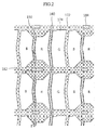
FIG. 2 is a plan view illustrating an in-cell touch type display panel in accordance with a first embodiment of the present invention; -
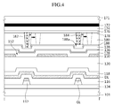
FIG. 3 is a sectional view illustrating the display panel having a touch sensing line, a stopper layer, and a column spacer illustrated inFIG. 2 ; -
FIG. 4 is a sectional view illustrating variation in the position of the column spacer due to external force in the display panel having the stopper layer illustrated inFIG. 3 ; and -
FIG. 5 is a plan view illustrating an in-cell touch type display panel in accordance with a second embodiment of the present invention. - Hereinafter, the embodiments of the present invention will be described in detail with reference to the accompanying drawings.
-
FIG. 1 is a block diagram illustrating an in-cell touch type display in accordance with one or more embodiments of the present invention. All the components of the in-cell touch type display according to all embodiments of the present invention are operatively coupled and configured. - The touch display illustrated in
FIG. 1 includes adata driver 194, agate driver 192, atouch driver 196, and a display panel. - The
data driver 194 converts digital data from a timing controller into an analogue data voltage in response to a data control signal from the timing controller, and supplies the analogue data voltage to data lines DL. - The
gate driver 192 sequentially drives gate lines GL of the display panel in response to a gate control signal from the timing controller. Thegate driver 192 supplies the scan pulse of a gate-on voltage for every corresponding scan period of each gate line GL, and supplies a gate-off voltage for the remaining period during which the other gate lines GL are driven. Thegate driver 192 is formed in a non-display area on one side or both sides of asubstrate 101, simultaneously with the manufacture of a thin film transistor (TFT) of each pixel. - The
touch driver 196 is connected to atouch sensing line 160 of the display panel, and receives a user touch signal from thetouch sensing line 160. Thetouch driver 196 detects whether or not a user touch is input and a touch position by sensing variation in capacitance attributable to the user touch. - The display panel displays an image using a plurality of pixels arranged in a matrix form. When a liquid crystal panel is used as the display panel, the display panel includes a
substrate 170 including a color filter, asubstrate 190 including a thin film transistor, and aliquid crystal layer 180 between thesubstrates FIGs. 2 and3 . - The
substrate 170 including a color filter includes ablack matrix 172,color filters 174, anovercoat layer 176, anupper alignment film 178, and first andsecond column spacers upper substrate 171 in sequence. - The
black matrix 172 serves to divide red, green, and blue sub-pixel areas from one another and to prevent light interference between the adjacent sub-pixel areas. Theblack matrix 172 is formed on theupper substrate 171 to overlap at least one of the gate line GL, the data line DL, thetouch sensing line 160, and the thin film transistor TFT. - The red (R), green (G), and blue (B)
color filters 174 are formed on theupper substrate 171 in the sub-pixel areas of the corresponding colors to create the corresponding colors. - The
overcoat layer 176 is formed over thecolor filters 174 and theblack matrix 172 using a transparent organic insulation material. Theovercoat layer 176 compensates for the height difference between thecolor filters 174 and theblack matrix 172. - The
first column spacer 182 is used as a gap spacer for maintaining a cell gap between the thinfilm transistor substrate 190 and thecolor filter substrate 170. To this end, thefirst column spacer 182 is formed to the same height as the cell gap to come into contact with alower alignment film 188, and has a greater area than thesecond column spacer 184. As such, the region of theblack matrix 172, which corresponds to thefirst column spacer 182, is greater than the region of theblack matrix 172, which corresponds to thesecond column spacer 184. - The
second column spacer 184 is formed to a lower height than thefirst column spacer 182, and is used as a push spacer, which does not come into contact with thelower alignment film 188. Thesecond column spacer 184 is used as a passage, which may be smoothly filled with liquid crystals upon the introduction of liquid crystals, and may allow theupper substrate 171 to be easily returned into an original state when pressure is applied to theupper substrate 171. To this end, thesecond column spacer 184 has a higher density than thefirst column spacer 182. - The thin
film transistor substrate 190 includes the thin film transistor TFT connected to the gate line GL and the data line DL, which cross each other to define a pixel area, apixel electrode 122, acommon electrode 136, thetouch sensing line 160, and astopper layer 150. - The thin film transistor TFT charges the
pixel electrode 122 with a data signal of the data line DL in response to a scan signal of the gate line GL, and maintains thepixel electrode 122 charged with the data signal. To this end, the thin film transistor TFT includes agate electrode 106, asource electrode 108, adrain electrode 110, and anactive layer 114 as illustrated inFIG. 3 . - The
gate electrode 106 overlaps a channel region of theactive layer 114 with agate insulation film 112 interposed therebetween. - The
source electrode 108 is connected to a source region of theactive layer 114 through a source contact hole CHs, which penetrates aninterlayer insulation film 116. - The
drain electrode 110 faces thesource electrode 108, and is connected to a drain region of theactive layer 114 through a drain contact hole CHd, which penetrates theinterlayer insulation film 116. In addition, thedrain electrode 110 is connected to thepixel electrode 122 through a pixel contact hole CHp. - The
active layer 114 is formed on abuffer layer 124, and forms a channel between thesource electrode 108 and thedrain electrode 110. Theactive layer 114 includes the channel region, the source region, and the drain region. The channel region overlaps thegate electrode 106 with thegate insulation film 112 interposed therebetween. An n-type or p-type dopant is introduced into the source region and the drain region. - The thin film transistor described above is protected by a first
protective film 118, which is formed of SiNx or SiOx. - The
pixel electrode 122 is formed on a thirdprotective film 138 in each pixel area, which is defined by the gate line GL and the data line DL crossing each other, to have a plurality ofslits 122S. Thepixel electrode 122 is electrically connected to thedrain electrode 110, which is exposed through the pixel contact hole CHp. - The
common electrode 136 is formed on a secondprotective film 128, and has anopening 134, which has a greater area than the pixel contact hole CHp, in a region overlapping the pixel contact hole CHp. Thecommon electrode 136 overlaps thepixel electrode 122 in each pixel area with the thirdprotective film 138 interposed therebetween. As such, thecommon electrode 136, to which a common voltage is supplied for a period during which an image is displayed, forms a fringe field in cooperation with thepixel electrode 122, to which a pixel voltage signal is supplied. Liquid crystal molecules, which are arranged between the thin film transistor substrate and the color filter substrate by the fringe field, are rotated by dielectric anisotropy. In addition, the transmittance of light passing through the pixel area changes depending on the degree of rotation of liquid crystal molecules, whereby gradation is realized. - In addition, the
common electrode 136 serves as a sensing electrode, which senses a user touch position for a touch sensing period, which is a non-display period during which no image is displayed. To this end, a plurality ofcommon electrodes 136 in block units is spaced apart from each other by a prescribed distance on thesubstrate 101 as illustrated inFIG. 1 . Each of thecommon electrodes 136 has a size corresponding to at least one pixel area in consideration of the area of the user touch. Thecommon electrode 136 is electrically connected to thetouch sensing line 160 through a touch contact hole CHt. Here, thetouch sensing line 160 transmits a user touch signal sensed by thecommon electrode 136 to thetouch driver 196. As such, when the user touches the display panel, touch capacitance is generated between thecommon electrodes 136. The position of the user touch is detected by comparing the touch capacitance in response to the user touch with a reference capacitance, and an operation depending on the detected touch position is performed. - Meanwhile, each
touch sensing line 160 is located on every unit pixel, which includes red (R), green (G) and blue (B) sub-pixels. Eachtouch sensing line 160 is formed to overlap the data line DL of at least one sub-pixel among the red (R), green (G) and blue (B) sub-pixels. - The
stopper layer 150, which is parallel to thetouch sensing line 160, is formed on either side of each of the first andsecond column spacers stopper layer 150 is formed to overlap the data line DL of any one sub-pixel among the two remaining sub-pixels excluding the data line DL of the sub-pixel that overlaps thetouch sensing line 160. For example, thetouch sensing line 160 overlaps the data line DL of the green (G) sub-pixel, and also overlaps theblack matrix 172, which is located between the red (R) and green (G) color filters 174. In addition, thestopper layer 150 overlaps the data line DL of the red (R) sub-pixel, and also overlaps theblack matrix 172, which is located between the red (R) and blue (B) color filters 174. - The
stopper layer 150 is formed on aplanarization layer 120, i.e. thestopper layer 150 may be formed on the same plane as thetouch sensing line 160, using a metal, such as Al, Cu, Cr, Mo or Ti, which may be the same material as thetouch sensing line 160. Accordingly, thestopper layer 150 may be formed simultaneously with thetouch sensing line 160 without an additional mask process, which may reduce the manufacturing costs. - In addition, each
stopper layer 150 is formed to be spaced apart from theadjacent stopper layer 150 with aspace 152 interposed therebetween, thespace 152 overlapping each of the first andsecond column spacers stopper layer 150 is spaced apart from theadjacent stopper layer 150 by a first distance in the region of theblack matrix 172, which overlaps the intersection of the gate line GL and the data line DL. As such, the respective upper surfaces of the second and thirdprotective films stopper layer 150, are recessed in the region corresponding to thespace 152, such that arecess 188a is formed in thelower alignment film 188, which is formed on the thirdprotective film 138. That is, the upper surface of thelower alignment film 188, corresponding to thespace 152, is formed close to the upper surface of theplanarization layer 120 than the upper surface of thelower alignment film 188 disposed on thestopper layer 150. - Each of the first and
second column spacers recess 188a of thelower alignment film 188, which corresponds to thespace 152 between the adjacent stopper layers 150. In this case, when external pressure is applied in the vertical direction, which is parallel to the longitudinal direction of the data line DL, as illustrated inFIG. 4 , the movement of the first orsecond column spacer recess 188a, which overlaps theblack matrix 172, due to the pressure. Therefore, damage to thelower alignment film 188 disposed in the pixel area may be prevented. Meanwhile, even if the first orsecond column spacer recess 188a in response to relatively strong external pressure, each of the first andsecond column spacers stopper layer 150, which overlaps theblack matrix 172. As such, it is possible to minimize the movement of the first andsecond column spacers lower alignment film 188. Contact between the first andsecond column spacers lower alignment film 188 located in the pixel area may be minimized, which may minimize damage to thelower alignment film 188 located in the pixel area. -
FIG. 5 is a plan view illustrating a display panel in accordance with a second embodiment of the present invention. - The display panel illustrated in
FIG. 5 includes the same constituent elements as those of the first embodiment of the present invention, except that it further includes asecond stopper layer 154, and therefore a detailed description related to the same constituent elements will be omitted below or may be brief. - The
second stopper layer 154 is formed to overlap theblack matrix layer 172, which is located between thetouch sensing line 160 and thefirst stopper layer 150. For example, thetouch sensing line 160 overlaps theblack matrix 172, which is located between the red (R) and green (G)color filters 174, and also overlaps the data line DL of the green (G) sub-pixel, which overlaps theblack matrix 172. Thefirst stopper layer 150 overlaps theblack matrix 172, which is located between the blue (B) and red (R)color filters 174, and also overlaps the data line DL of the red (R) sub-pixel, which overlaps theblack matrix 172. Thesecond stopper layer 154 overlaps theblack matrix 172, which is located between the green (G) and blue (B)color filters 174, and also overlaps the data line DL of the blue (B) sub-pixel, which overlaps theblack matrix 172. - The first and second stopper layers 150 and 154 are formed on the
planarization layer 120, which is in the same plane as thetouch sensing line 160, using a metal, such as Al, Cu, Cr, Mo or Ti, which is the same material as thetouch sensing line 160. Accordingly, the first and second stopper layers 150 and 154 may be formed simultaneously with thetouch sensing line 160 without an additional mask process, which may reduce the manufacturing costs. - In addition, each
first stopper layer 150 is spaced apart from an adjacentfirst stopper layer 150 with a first space, which has a first distance d1, interposed therebetween in the region of theblack matrix 172, which overlaps the intersection of the gate line GL and the data line DL. Eachsecond stopper layer 154 is spaced apart from an adjacentsecond stopper layer 154 with a second space, which has a second distance d2, which is smaller than the first distance d1, interposed therebetween in the region of theblack matrix 172, which overlaps the intersection of the gate line GL and the data line DL. As such, thesecond stopper layer 154 faces the left side of each of the first andsecond column spacers touch sensing line 160 faces the right side of each of the first andsecond column spacers first stopper layer 150 faces the upper side and the lower side of each of the first andsecond column spacers second stopper layer 154 and thetouch sensing line 160 limit the movement of the first andsecond column spacers first stopper layer 150 limits the movement of the first andsecond column spacers second column spacers lower alignment film 188 in the pixel area, and therefore, it is possible to prevent damage to thelower alignment film 188 located in the pixel area. - It can be appreciated that the liquid crystal display panel in accordance with the first and second embodiments of the present invention exhibits no movement of the first and
second column spacers Table 1 Related Art First Embodiment Second Embodiment Average Generation force (N) 0.4 0.47 0.6 - Meanwhile, the thin film transistor substrate in accordance with the embodiments of the present invention is located to be opposite the color filter substrate with the liquid crystal layer interposed therebetween, whereby the liquid crystal display panel is completed. At this time, although the fringe field structure has been described by way of example in the present invention, a horizontal field type structure or vertical field type structure may also be applied to all liquid crystal display panels.
- As is apparent from the above description, according to the embodiments of the present invention, a plurality of stopper layers, formed on the same plane as a touch sensing line, is spaced apart from each other with a space therebetween, and a column spacer is located to overlap the space. The column spacer according to the present invention is inserted into a recess in an alignment film, which corresponds to the space. As such, even if external pressure is applied, movement of the column spacer is limited within the recess, which overlaps a black matrix, which may prevent damage to the alignment film. Thereby, it is possible to prevent light leakage without a reduction in an aperture ratio. In addition, even if the column spacer moves out of the recess because the external pressure is strong, the column spacer slides on the stopper layer, which may minimize movement of the column spacer located in a pixel area to the alignment film. In addition, because the stopper layers are formed of the same material as the touch sensing line, simultaneously with the formation of the touch sensing line, no additional mask process is required and no half-tone mask is required, which may prevent an increase in manufacturing costs.
Claims (15)
- A display panel comprising:a plurality of first stopper layers (150) located on the first substrate (190)and spaced apart from each other with a space (152) therebetween; anda plurality of column spacers (182, 184) located on the second substrate (170) opposite to the space (152) between adjacent first stopper layers (150) on the first substrate (190).
- The display panel according to claim 1, further comprising:a plurality of first to third sub-pixel areas (R, G, B);wherein the first stopper layers (150) are located between the first and third sub-pixel areas (R, B).
- The display panel according to claim 1 or 2, further comprising:a plurality of touch sensing lines (160) connected to touch sensing electrodes (136) and located on the first substrate (190).
- The display panel according to claim 3, wherein the touch sensing lines (160) are located between the first and second sub-pixel areas (R, G).
- The display panel according to claim 3 or 4, wherein the first stopper layers (150) are located on a same layer and/or made of a same material as the touch sensing lines (160).
- The display panel according to any one of claims 3 to 5, wherein the touch sensing electrodes (136) are common electrodes (136) of the display panel.
- The display panel according to any one of the preceding claims, further comprising:a black matrix (172) on the second substrate (170);wherein the first stopper layers (150) are located opposite to the black matrix (172).
- The display panel according to any one of claims 2 to 7, further comprising:a plurality of gate lines (GL) and a plurality of data lines (DL) crossing each other on the first substrate (190) to define the first to third sub-pixel areas (R, G, B),wherein the first stopper layers (150) are spaced apart from each other in direction of the data lines (DL) and/or wherein the first stopper layers (150) are located on the data lines (DL).
- The display panel according to any one of claim 8, further comprising:a plurality of second stopper layers (154) located between the second and third sub-pixel areas (G, B).
- The display panel according to claim 9, wherein the second stopper layers (154) are formed of a same material and/or on a same layer as the first stopper layers (150).
- The display panel according to claim 9 or 10, wherein the second stopper layers (154) are located on the data lines and/or spaced apart from each other in direction of the data lines (DL).
- The display panel according to any one of claims 8 to 11, wherein wherein a distance (d2) between adjacent second stopper layers (154) is smaller than a distance (d1) between adjacent first stopper layers (150) in parallel to the data lines (DL).
- The display panel according to any one of claims 8 to 12, wherein the first stopper layers (150) and/or the second stopper layers (154) expose crossings of the data lines (DL) and the gate lines (GL).
- The display panel according to any one of the preceding claims, wherein in the space (152) between the first stopper layers (150), a recess (188a) is formed in a lower alignment film (188) on the first substrate (190) and the column spacers (182, 184) are located opposite to the recesses (188a), respectively.
- The display panel according to claim 14, wherein the plurality of column spacers (182, 184) includes a plurality of first column spacers (182) for maintaining a cell gap between the first and the second substrates (170, 190) and a plurality of second column spacers (184) having a height less than the first column spacers (182).
Applications Claiming Priority (1)
| Application Number | Priority Date | Filing Date | Title |
|---|---|---|---|
| KR1020150106991A KR102316560B1 (en) | 2015-07-29 | 2015-07-29 | Substrate including thin film transistor and display panel having the smae |
Publications (3)
| Publication Number | Publication Date |
|---|---|
| EP3125029A2 true EP3125029A2 (en) | 2017-02-01 |
| EP3125029A3 EP3125029A3 (en) | 2017-02-15 |
| EP3125029B1 EP3125029B1 (en) | 2018-06-13 |
Family
ID=56555292
Family Applications (1)
| Application Number | Title | Priority Date | Filing Date |
|---|---|---|---|
| EP16181826.5A Active EP3125029B1 (en) | 2015-07-29 | 2016-07-29 | Display panel having substrates |
Country Status (4)
| Country | Link |
|---|---|
| US (1) | US10198105B2 (en) |
| EP (1) | EP3125029B1 (en) |
| KR (1) | KR102316560B1 (en) |
| CN (1) | CN106405957B (en) |
Families Citing this family (20)
| Publication number | Priority date | Publication date | Assignee | Title |
|---|---|---|---|---|
| US9113301B1 (en) | 2014-06-13 | 2015-08-18 | Snapchat, Inc. | Geo-location based event gallery |
| CN206460240U (en) * | 2017-02-09 | 2017-09-01 | 中华映管股份有限公司 | Touch control display device |
| US10582277B2 (en) | 2017-03-27 | 2020-03-03 | Snap Inc. | Generating a stitched data stream |
| CN106802517B (en) * | 2017-04-12 | 2019-07-02 | 京东方科技集团股份有限公司 | A liquid crystal display panel and display device |
| CN106918960B (en) * | 2017-05-11 | 2020-09-25 | 厦门天马微电子有限公司 | Display panel and display device |
| KR102423865B1 (en) * | 2017-12-04 | 2022-07-21 | 엘지디스플레이 주식회사 | Display device having touch sensor |
| JP6968710B2 (en) * | 2018-01-11 | 2021-11-17 | 株式会社ジャパンディスプレイ | Display device |
| JP6640252B2 (en) * | 2018-01-19 | 2020-02-05 | シャープ株式会社 | LCD panel |
| TWI679565B (en) * | 2018-09-04 | 2019-12-11 | 友達光電股份有限公司 | Touch panel |
| TWI667522B (en) * | 2018-09-06 | 2019-08-01 | 友達光電股份有限公司 | Pixel structure |
| CN109637362B (en) * | 2019-01-31 | 2021-07-09 | 厦门天马微电子有限公司 | Display panel and display device |
| KR102866118B1 (en) * | 2019-11-28 | 2025-09-30 | 엘지디스플레이 주식회사 | Touch display device |
| CN110867151B (en) * | 2019-11-29 | 2022-07-05 | 合肥维信诺科技有限公司 | Display mother board, display panel and electronic leakage testing method |
| CN111766977B (en) * | 2020-06-12 | 2021-08-24 | 惠州市华星光电技术有限公司 | Touch panel and touch display device |
| KR102915438B1 (en) * | 2020-10-30 | 2026-01-20 | 엘지디스플레이 주식회사 | Touch display device |
| JP2022076254A (en) * | 2020-11-09 | 2022-05-19 | 株式会社ジャパンディスプレイ | Display device and watch |
| DE112021006307T5 (en) * | 2021-01-12 | 2023-09-21 | Japan Display Inc. | DISPLAY DEVICE |
| WO2023039823A1 (en) * | 2021-09-17 | 2023-03-23 | 京东方科技集团股份有限公司 | Display panel and preparation method therefor, and display device |
| CN114115614A (en) * | 2021-11-30 | 2022-03-01 | 合肥维信诺科技有限公司 | Touch panel and display device |
| CN115268132B (en) * | 2022-07-19 | 2023-08-22 | 武汉华星光电技术有限公司 | Display device and display panel thereof |
Family Cites Families (8)
| Publication number | Priority date | Publication date | Assignee | Title |
|---|---|---|---|---|
| KR101157954B1 (en) * | 2005-09-28 | 2012-06-22 | 엘지디스플레이 주식회사 | Liquid Crystal Display Device and Method for Manufacturing the Same |
| KR20070078178A (en) * | 2006-01-26 | 2007-07-31 | 삼성전자주식회사 | Liquid crystal display panel |
| KR101735386B1 (en) * | 2010-06-25 | 2017-05-30 | 엘지디스플레이 주식회사 | Liquid crystal display device having touch sensor embedded therein, method for driving the same and method for fabricating the same |
| KR102008779B1 (en) * | 2012-10-22 | 2019-08-09 | 엘지디스플레이 주식회사 | Display Device With Integrated Touch Screen and Method for Driving The Same |
| CN103207719A (en) * | 2013-03-28 | 2013-07-17 | 北京京东方光电科技有限公司 | Capacitive inlaid touch screen and display device |
| CN103294317B (en) * | 2013-05-31 | 2016-03-30 | 京东方科技集团股份有限公司 | A kind of array base palte, contact panel and display device |
| KR20150026586A (en) * | 2013-09-03 | 2015-03-11 | 엘지디스플레이 주식회사 | Liquid crystal display device having column spacer |
| JP2015075606A (en) * | 2013-10-08 | 2015-04-20 | 株式会社ジャパンディスプレイ | Liquid crystal display device |
-
2015
- 2015-07-29 KR KR1020150106991A patent/KR102316560B1/en active Active
-
2016
- 2016-07-25 US US15/218,723 patent/US10198105B2/en active Active
- 2016-07-26 CN CN201610596381.3A patent/CN106405957B/en active Active
- 2016-07-29 EP EP16181826.5A patent/EP3125029B1/en active Active
Non-Patent Citations (1)
| Title |
|---|
| None |
Also Published As
| Publication number | Publication date |
|---|---|
| CN106405957B (en) | 2019-11-12 |
| CN106405957A (en) | 2017-02-15 |
| KR20170014135A (en) | 2017-02-08 |
| KR102316560B1 (en) | 2021-10-25 |
| US10198105B2 (en) | 2019-02-05 |
| US20170031488A1 (en) | 2017-02-02 |
| EP3125029A3 (en) | 2017-02-15 |
| EP3125029B1 (en) | 2018-06-13 |
Similar Documents
| Publication | Publication Date | Title |
|---|---|---|
| EP3125029B1 (en) | Display panel having substrates | |
| US9941303B1 (en) | Array substrate, display panel and display device | |
| EP2980636B1 (en) | Liquid crystal display panel | |
| US9780126B2 (en) | Z-inversion type display device and method of manufacturing the same | |
| US9429795B2 (en) | Display panel having particular spacer arrangement | |
| US20170038653A1 (en) | Method for manufacturing coa liquid crystal panel and coa liquid crystal panel | |
| JP2018527623A (en) | VA type COA liquid crystal display panel | |
| US10672801B2 (en) | TFT substrate | |
| US7876389B2 (en) | Display substrate and display device having the same | |
| US8149228B2 (en) | Active matrix substrate | |
| US8531641B2 (en) | Liquid crystal display device and method of manufacturing the same | |
| TWI402582B (en) | Liquid crystal display device with wide viewing angle | |
| TWI407222B (en) | Pixel array, polymer stablized alignment liquid crystal display panel, and pixel array driving method | |
| US8253916B2 (en) | Liquid crystal display device | |
| CN105278189B (en) | The pel array of liquid crystal display | |
| US20140347586A1 (en) | Liquid crystal display device | |
| JP2003207803A (en) | Horizontal electric field type active matrix liquid crystal display device | |
| JPWO2009104346A1 (en) | Active matrix substrate and liquid crystal display device | |
| US9041895B2 (en) | Display apparatus having spacers with different heights and different upper and lower surface areas | |
| KR102605983B1 (en) | Display apparatus | |
| KR20160042256A (en) | Liquid Crystal Display Device Preventing From Leakage Light and Method for Preparing the Same | |
| US20210341776A1 (en) | Display panel and method of manufacturing the same | |
| JP2009063696A (en) | Liquid crystal display | |
| KR20230169057A (en) | Liquid Crystal Display Device | |
| US20090135358A1 (en) | Display device |
Legal Events
| Date | Code | Title | Description |
|---|---|---|---|
| PUAI | Public reference made under article 153(3) epc to a published international application that has entered the european phase |
Free format text: ORIGINAL CODE: 0009012 |
|
| PUAL | Search report despatched |
Free format text: ORIGINAL CODE: 0009013 |
|
| 17P | Request for examination filed |
Effective date: 20160729 |
|
| AK | Designated contracting states |
Kind code of ref document: A2 Designated state(s): AL AT BE BG CH CY CZ DE DK EE ES FI FR GB GR HR HU IE IS IT LI LT LU LV MC MK MT NL NO PL PT RO RS SE SI SK SM TR |
|
| AX | Request for extension of the european patent |
Extension state: BA ME |
|
| AK | Designated contracting states |
Kind code of ref document: A3 Designated state(s): AL AT BE BG CH CY CZ DE DK EE ES FI FR GB GR HR HU IE IS IT LI LT LU LV MC MK MT NL NO PL PT RO RS SE SI SK SM TR |
|
| AX | Request for extension of the european patent |
Extension state: BA ME |
|
| RIC1 | Information provided on ipc code assigned before grant |
Ipc: G02F 1/1339 20060101ALI20170110BHEP Ipc: G02F 1/1362 20060101ALN20170110BHEP Ipc: G02F 1/1337 20060101ALN20170110BHEP Ipc: G02F 1/1335 20060101ALN20170110BHEP Ipc: G06F 3/041 20060101ALN20170110BHEP Ipc: G02F 1/1333 20060101AFI20170110BHEP |
|
| RBV | Designated contracting states (corrected) |
Designated state(s): AL AT BE BG CH CY CZ DE DK EE ES FI FR GB GR HR HU IE IS IT LI LT LU LV MC MK MT NL NO PL PT RO RS SE SI SK SM TR |
|
| RIC1 | Information provided on ipc code assigned before grant |
Ipc: G02F 1/1333 20060101AFI20171116BHEP Ipc: G06F 3/041 20060101ALN20171116BHEP Ipc: G02F 1/1335 20060101ALN20171116BHEP Ipc: G02F 1/1362 20060101ALN20171116BHEP Ipc: G02F 1/1339 20060101ALI20171116BHEP Ipc: G06F 3/044 20060101ALN20171116BHEP Ipc: G02F 1/1337 20060101ALN20171116BHEP |
|
| GRAP | Despatch of communication of intention to grant a patent |
Free format text: ORIGINAL CODE: EPIDOSNIGR1 |
|
| RIC1 | Information provided on ipc code assigned before grant |
Ipc: G02F 1/1337 20060101ALN20171124BHEP Ipc: G06F 3/041 20060101ALN20171124BHEP Ipc: G02F 1/1333 20060101AFI20171124BHEP Ipc: G02F 1/1362 20060101ALN20171124BHEP Ipc: G02F 1/1339 20060101ALI20171124BHEP Ipc: G02F 1/1335 20060101ALN20171124BHEP Ipc: G06F 3/044 20060101ALN20171124BHEP |
|
| RIC1 | Information provided on ipc code assigned before grant |
Ipc: G02F 1/1362 20060101ALN20171206BHEP Ipc: G02F 1/1337 20060101ALN20171206BHEP Ipc: G02F 1/1335 20060101ALN20171206BHEP Ipc: G02F 1/1333 20060101AFI20171206BHEP Ipc: G06F 3/041 20060101ALN20171206BHEP Ipc: G06F 3/044 20060101ALN20171206BHEP Ipc: G02F 1/1339 20060101ALI20171206BHEP |
|
| INTG | Intention to grant announced |
Effective date: 20180102 |
|
| GRAS | Grant fee paid |
Free format text: ORIGINAL CODE: EPIDOSNIGR3 |
|
| GRAA | (expected) grant |
Free format text: ORIGINAL CODE: 0009210 |
|
| AK | Designated contracting states |
Kind code of ref document: B1 Designated state(s): AL AT BE BG CH CY CZ DE DK EE ES FI FR GB GR HR HU IE IS IT LI LT LU LV MC MK MT NL NO PL PT RO RS SE SI SK SM TR |
|
| REG | Reference to a national code |
Ref country code: GB Ref legal event code: FG4D |
|
| REG | Reference to a national code |
Ref country code: CH Ref legal event code: EP Ref country code: AT Ref legal event code: REF Ref document number: 1009078 Country of ref document: AT Kind code of ref document: T Effective date: 20180615 |
|
| REG | Reference to a national code |
Ref country code: IE Ref legal event code: FG4D |
|
| REG | Reference to a national code |
Ref country code: DE Ref legal event code: R096 Ref document number: 602016003516 Country of ref document: DE |
|
| REG | Reference to a national code |
Ref country code: FR Ref legal event code: PLFP Year of fee payment: 3 |
|
| REG | Reference to a national code |
Ref country code: NL Ref legal event code: FP |
|
| REG | Reference to a national code |
Ref country code: LT Ref legal event code: MG4D |
|
| PG25 | Lapsed in a contracting state [announced via postgrant information from national office to epo] |
Ref country code: BG Free format text: LAPSE BECAUSE OF FAILURE TO SUBMIT A TRANSLATION OF THE DESCRIPTION OR TO PAY THE FEE WITHIN THE PRESCRIBED TIME-LIMIT Effective date: 20180913 Ref country code: LT Free format text: LAPSE BECAUSE OF FAILURE TO SUBMIT A TRANSLATION OF THE DESCRIPTION OR TO PAY THE FEE WITHIN THE PRESCRIBED TIME-LIMIT Effective date: 20180613 Ref country code: CY Free format text: LAPSE BECAUSE OF FAILURE TO SUBMIT A TRANSLATION OF THE DESCRIPTION OR TO PAY THE FEE WITHIN THE PRESCRIBED TIME-LIMIT Effective date: 20180613 Ref country code: SE Free format text: LAPSE BECAUSE OF FAILURE TO SUBMIT A TRANSLATION OF THE DESCRIPTION OR TO PAY THE FEE WITHIN THE PRESCRIBED TIME-LIMIT Effective date: 20180613 Ref country code: FI Free format text: LAPSE BECAUSE OF FAILURE TO SUBMIT A TRANSLATION OF THE DESCRIPTION OR TO PAY THE FEE WITHIN THE PRESCRIBED TIME-LIMIT Effective date: 20180613 Ref country code: ES Free format text: LAPSE BECAUSE OF FAILURE TO SUBMIT A TRANSLATION OF THE DESCRIPTION OR TO PAY THE FEE WITHIN THE PRESCRIBED TIME-LIMIT Effective date: 20180613 Ref country code: NO Free format text: LAPSE BECAUSE OF FAILURE TO SUBMIT A TRANSLATION OF THE DESCRIPTION OR TO PAY THE FEE WITHIN THE PRESCRIBED TIME-LIMIT Effective date: 20180913 |
|
| PG25 | Lapsed in a contracting state [announced via postgrant information from national office to epo] |
Ref country code: RS Free format text: LAPSE BECAUSE OF FAILURE TO SUBMIT A TRANSLATION OF THE DESCRIPTION OR TO PAY THE FEE WITHIN THE PRESCRIBED TIME-LIMIT Effective date: 20180613 Ref country code: LV Free format text: LAPSE BECAUSE OF FAILURE TO SUBMIT A TRANSLATION OF THE DESCRIPTION OR TO PAY THE FEE WITHIN THE PRESCRIBED TIME-LIMIT Effective date: 20180613 Ref country code: HR Free format text: LAPSE BECAUSE OF FAILURE TO SUBMIT A TRANSLATION OF THE DESCRIPTION OR TO PAY THE FEE WITHIN THE PRESCRIBED TIME-LIMIT Effective date: 20180613 Ref country code: GR Free format text: LAPSE BECAUSE OF FAILURE TO SUBMIT A TRANSLATION OF THE DESCRIPTION OR TO PAY THE FEE WITHIN THE PRESCRIBED TIME-LIMIT Effective date: 20180914 |
|
| REG | Reference to a national code |
Ref country code: AT Ref legal event code: MK05 Ref document number: 1009078 Country of ref document: AT Kind code of ref document: T Effective date: 20180613 |
|
| PG25 | Lapsed in a contracting state [announced via postgrant information from national office to epo] |
Ref country code: SK Free format text: LAPSE BECAUSE OF FAILURE TO SUBMIT A TRANSLATION OF THE DESCRIPTION OR TO PAY THE FEE WITHIN THE PRESCRIBED TIME-LIMIT Effective date: 20180613 Ref country code: RO Free format text: LAPSE BECAUSE OF FAILURE TO SUBMIT A TRANSLATION OF THE DESCRIPTION OR TO PAY THE FEE WITHIN THE PRESCRIBED TIME-LIMIT Effective date: 20180613 Ref country code: PL Free format text: LAPSE BECAUSE OF FAILURE TO SUBMIT A TRANSLATION OF THE DESCRIPTION OR TO PAY THE FEE WITHIN THE PRESCRIBED TIME-LIMIT Effective date: 20180613 Ref country code: CZ Free format text: LAPSE BECAUSE OF FAILURE TO SUBMIT A TRANSLATION OF THE DESCRIPTION OR TO PAY THE FEE WITHIN THE PRESCRIBED TIME-LIMIT Effective date: 20180613 Ref country code: IS Free format text: LAPSE BECAUSE OF FAILURE TO SUBMIT A TRANSLATION OF THE DESCRIPTION OR TO PAY THE FEE WITHIN THE PRESCRIBED TIME-LIMIT Effective date: 20181013 Ref country code: AT Free format text: LAPSE BECAUSE OF FAILURE TO SUBMIT A TRANSLATION OF THE DESCRIPTION OR TO PAY THE FEE WITHIN THE PRESCRIBED TIME-LIMIT Effective date: 20180613 Ref country code: EE Free format text: LAPSE BECAUSE OF FAILURE TO SUBMIT A TRANSLATION OF THE DESCRIPTION OR TO PAY THE FEE WITHIN THE PRESCRIBED TIME-LIMIT Effective date: 20180613 |
|
| PG25 | Lapsed in a contracting state [announced via postgrant information from national office to epo] |
Ref country code: IT Free format text: LAPSE BECAUSE OF FAILURE TO SUBMIT A TRANSLATION OF THE DESCRIPTION OR TO PAY THE FEE WITHIN THE PRESCRIBED TIME-LIMIT Effective date: 20180613 Ref country code: SM Free format text: LAPSE BECAUSE OF FAILURE TO SUBMIT A TRANSLATION OF THE DESCRIPTION OR TO PAY THE FEE WITHIN THE PRESCRIBED TIME-LIMIT Effective date: 20180613 |
|
| REG | Reference to a national code |
Ref country code: DE Ref legal event code: R097 Ref document number: 602016003516 Country of ref document: DE |
|
| PG25 | Lapsed in a contracting state [announced via postgrant information from national office to epo] |
Ref country code: LU Free format text: LAPSE BECAUSE OF NON-PAYMENT OF DUE FEES Effective date: 20180729 Ref country code: MC Free format text: LAPSE BECAUSE OF FAILURE TO SUBMIT A TRANSLATION OF THE DESCRIPTION OR TO PAY THE FEE WITHIN THE PRESCRIBED TIME-LIMIT Effective date: 20180613 |
|
| REG | Reference to a national code |
Ref country code: BE Ref legal event code: MM Effective date: 20180731 |
|
| PLBE | No opposition filed within time limit |
Free format text: ORIGINAL CODE: 0009261 |
|
| STAA | Information on the status of an ep patent application or granted ep patent |
Free format text: STATUS: NO OPPOSITION FILED WITHIN TIME LIMIT |
|
| REG | Reference to a national code |
Ref country code: IE Ref legal event code: MM4A |
|
| 26N | No opposition filed |
Effective date: 20190314 |
|
| PG25 | Lapsed in a contracting state [announced via postgrant information from national office to epo] |
Ref country code: DK Free format text: LAPSE BECAUSE OF FAILURE TO SUBMIT A TRANSLATION OF THE DESCRIPTION OR TO PAY THE FEE WITHIN THE PRESCRIBED TIME-LIMIT Effective date: 20180613 Ref country code: SI Free format text: LAPSE BECAUSE OF FAILURE TO SUBMIT A TRANSLATION OF THE DESCRIPTION OR TO PAY THE FEE WITHIN THE PRESCRIBED TIME-LIMIT Effective date: 20180613 Ref country code: BE Free format text: LAPSE BECAUSE OF NON-PAYMENT OF DUE FEES Effective date: 20180731 |
|
| PG25 | Lapsed in a contracting state [announced via postgrant information from national office to epo] |
Ref country code: IE Free format text: LAPSE BECAUSE OF NON-PAYMENT OF DUE FEES Effective date: 20180729 |
|
| PG25 | Lapsed in a contracting state [announced via postgrant information from national office to epo] |
Ref country code: AL Free format text: LAPSE BECAUSE OF FAILURE TO SUBMIT A TRANSLATION OF THE DESCRIPTION OR TO PAY THE FEE WITHIN THE PRESCRIBED TIME-LIMIT Effective date: 20180613 |
|
| PG25 | Lapsed in a contracting state [announced via postgrant information from national office to epo] |
Ref country code: MT Free format text: LAPSE BECAUSE OF NON-PAYMENT OF DUE FEES Effective date: 20180729 |
|
| REG | Reference to a national code |
Ref country code: CH Ref legal event code: PL |
|
| PG25 | Lapsed in a contracting state [announced via postgrant information from national office to epo] |
Ref country code: TR Free format text: LAPSE BECAUSE OF FAILURE TO SUBMIT A TRANSLATION OF THE DESCRIPTION OR TO PAY THE FEE WITHIN THE PRESCRIBED TIME-LIMIT Effective date: 20180613 |
|
| PG25 | Lapsed in a contracting state [announced via postgrant information from national office to epo] |
Ref country code: LI Free format text: LAPSE BECAUSE OF NON-PAYMENT OF DUE FEES Effective date: 20190731 Ref country code: CH Free format text: LAPSE BECAUSE OF NON-PAYMENT OF DUE FEES Effective date: 20190731 Ref country code: PT Free format text: LAPSE BECAUSE OF FAILURE TO SUBMIT A TRANSLATION OF THE DESCRIPTION OR TO PAY THE FEE WITHIN THE PRESCRIBED TIME-LIMIT Effective date: 20180613 |
|
| PG25 | Lapsed in a contracting state [announced via postgrant information from national office to epo] |
Ref country code: HU Free format text: LAPSE BECAUSE OF FAILURE TO SUBMIT A TRANSLATION OF THE DESCRIPTION OR TO PAY THE FEE WITHIN THE PRESCRIBED TIME-LIMIT; INVALID AB INITIO Effective date: 20160729 Ref country code: MK Free format text: LAPSE BECAUSE OF NON-PAYMENT OF DUE FEES Effective date: 20180613 |
|
| REG | Reference to a national code |
Ref country code: DE Ref legal event code: R082 Ref document number: 602016003516 Country of ref document: DE Representative=s name: TER MEER STEINMEISTER & PARTNER PATENTANWAELTE, DE |
|
| PGFP | Annual fee paid to national office [announced via postgrant information from national office to epo] |
Ref country code: NL Payment date: 20250520 Year of fee payment: 10 |
|
| PGFP | Annual fee paid to national office [announced via postgrant information from national office to epo] |
Ref country code: GB Payment date: 20250520 Year of fee payment: 10 |
|
| PGFP | Annual fee paid to national office [announced via postgrant information from national office to epo] |
Ref country code: FR Payment date: 20250521 Year of fee payment: 10 |
|
| PGFP | Annual fee paid to national office [announced via postgrant information from national office to epo] |
Ref country code: DE Payment date: 20250520 Year of fee payment: 10 |