EP3121817A1 - Resistive memory apparatus and writing method thereof - Google Patents
Resistive memory apparatus and writing method thereof Download PDFInfo
- Publication number
- EP3121817A1 EP3121817A1 EP15192012.1A EP15192012A EP3121817A1 EP 3121817 A1 EP3121817 A1 EP 3121817A1 EP 15192012 A EP15192012 A EP 15192012A EP 3121817 A1 EP3121817 A1 EP 3121817A1
- Authority
- EP
- European Patent Office
- Prior art keywords
- resistive memory
- memory cell
- data
- current
- reset
- Prior art date
- Legal status (The legal status is an assumption and is not a legal conclusion. Google has not performed a legal analysis and makes no representation as to the accuracy of the status listed.)
- Granted
Links
Images

Classifications
-
- G—PHYSICS
- G11—INFORMATION STORAGE
- G11C—STATIC STORES
- G11C13/00—Digital stores characterised by the use of storage elements not covered by groups G11C11/00, G11C23/00, or G11C25/00
- G11C13/0002—Digital stores characterised by the use of storage elements not covered by groups G11C11/00, G11C23/00, or G11C25/00 using resistive RAM [RRAM] elements
- G11C13/0021—Auxiliary circuits
- G11C13/0069—Writing or programming circuits or methods
-
- G—PHYSICS
- G11—INFORMATION STORAGE
- G11C—STATIC STORES
- G11C13/00—Digital stores characterised by the use of storage elements not covered by groups G11C11/00, G11C23/00, or G11C25/00
- G11C13/0002—Digital stores characterised by the use of storage elements not covered by groups G11C11/00, G11C23/00, or G11C25/00 using resistive RAM [RRAM] elements
- G11C13/0021—Auxiliary circuits
- G11C13/0064—Verifying circuits or methods
-
- G—PHYSICS
- G11—INFORMATION STORAGE
- G11C—STATIC STORES
- G11C13/00—Digital stores characterised by the use of storage elements not covered by groups G11C11/00, G11C23/00, or G11C25/00
- G11C13/0002—Digital stores characterised by the use of storage elements not covered by groups G11C11/00, G11C23/00, or G11C25/00 using resistive RAM [RRAM] elements
- G11C13/0021—Auxiliary circuits
- G11C13/0064—Verifying circuits or methods
- G11C2013/0066—Verify correct writing whilst writing is in progress, e.g. by detecting onset or cessation of current flow in cell and using the detector output to terminate writing
-
- G—PHYSICS
- G11—INFORMATION STORAGE
- G11C—STATIC STORES
- G11C13/00—Digital stores characterised by the use of storage elements not covered by groups G11C11/00, G11C23/00, or G11C25/00
- G11C13/0002—Digital stores characterised by the use of storage elements not covered by groups G11C11/00, G11C23/00, or G11C25/00 using resistive RAM [RRAM] elements
- G11C13/0021—Auxiliary circuits
- G11C13/0069—Writing or programming circuits or methods
- G11C2013/0073—Write using bi-directional cell biasing
-
- G—PHYSICS
- G11—INFORMATION STORAGE
- G11C—STATIC STORES
- G11C13/00—Digital stores characterised by the use of storage elements not covered by groups G11C11/00, G11C23/00, or G11C25/00
- G11C13/0002—Digital stores characterised by the use of storage elements not covered by groups G11C11/00, G11C23/00, or G11C25/00 using resistive RAM [RRAM] elements
- G11C13/0021—Auxiliary circuits
- G11C13/0069—Writing or programming circuits or methods
- G11C2013/0076—Write operation performed depending on read result
-
- G—PHYSICS
- G11—INFORMATION STORAGE
- G11C—STATIC STORES
- G11C13/00—Digital stores characterised by the use of storage elements not covered by groups G11C11/00, G11C23/00, or G11C25/00
- G11C13/0002—Digital stores characterised by the use of storage elements not covered by groups G11C11/00, G11C23/00, or G11C25/00 using resistive RAM [RRAM] elements
- G11C13/0021—Auxiliary circuits
- G11C13/0069—Writing or programming circuits or methods
- G11C2013/0078—Write using current through the cell
-
- G—PHYSICS
- G11—INFORMATION STORAGE
- G11C—STATIC STORES
- G11C13/00—Digital stores characterised by the use of storage elements not covered by groups G11C11/00, G11C23/00, or G11C25/00
- G11C13/0002—Digital stores characterised by the use of storage elements not covered by groups G11C11/00, G11C23/00, or G11C25/00 using resistive RAM [RRAM] elements
- G11C13/0021—Auxiliary circuits
- G11C13/0069—Writing or programming circuits or methods
- G11C2013/0092—Write characterized by the shape, e.g. form, length, amplitude of the write pulse
Definitions
- the invention relates to a memory apparatus and a writing method thereof, and particularly relates to a resistive memory apparatus and a writing method thereof.
- a non-volatile memory has an advantage that data stored therein is not disappeared after power off, so that it serves as a necessary memory element for maintaining a normal operation of many electronic products.
- a resistive random access memory is a kind of non-volatile memory positively developed in the industry, which has advantages of low write operation voltage, short write and erase time, long memory time, non-destructive reading, multi-state memory, simple structure and small occupation area, etc., and has a great application potential in personal computers and electronic equipment in the future.
- the resistive random access memory can change a width of a filament path according to magnitude and polarity of an applied pulse voltage, so as to set a resistance value to a low resistance state (LRS) or a high resistance state (HRS) in a reversible and non-volatile manner to respectively represent stored data of different logic levels.
- LRS low resistance state
- HRS high resistance state
- a reset pulse can be applied to narrow the width of the filament path to achieve the HRS.
- a set pulse with an opposite polarity can be applied to broaden the width of the filament path to achieve the LRS. In this way, when the data is read, the data of logic 1 or logic 0 can be read according to a reading current of a different magnitude generated under different resistance states.
- the filament path in a variable resistance element may have a sharp contour after the set pulse is applied thereto, such that a filament path with an excessively large width at one end and an excessively small width at another end is formed, which results in a problem of electromigration (EM).
- EM electromigration
- the narrower a place in the filament path is, the higher a current density at the place is, and the higher an electric field thereof is, which leads to a phenomenon that metal atoms move towards an electron flowing direction along grain boundaries of the variable resistance element itself.
- the electromigration is continuously increased, the current density is accordingly increased to aggravate the situation. If the electromigration is too severe, the variable resistance element can be broken to form an open circuit, such that data cannot be correctly written.
- the invention is directed to a resistive memory apparatus and a writing method thereof, by which data is able to be correctly written.
- the invention provides a writing method of a resistive memory apparatus, which includes following steps.
- Logic data is received, and a corresponding resistive memory cell is selected.
- a logic level of the logic data is determined.
- the logic data is in a first logic level, where a first reading current of the corresponding resistive memory cell is greater than a first reference current, a set pulse and a reset pulse are provided to the resistive memory cell during a writing period. Polarities of the reset pulse and the set pulse are opposite.
- the reset pulse is typically provided to the resistive memory cell during the writing period, so as to generate a second reading current smaller than a second reference current when a reading voltage is applied to the resistive memory cell during a verification period.
- the set pulse is applied before re-applying the reset pulse.
- the invention provides a resistive memory apparatus including a resistive memory cell array, a current verification unit and a control unit.
- the resistive memory cell array includes a plurality of resistive memory cells.
- the control unit is coupled to the resistive memory cell array.
- the control unit receives logic data, and selects a corresponding resistive memory cell from the resistive memory cells.
- the control unit determines a logic level of the logic data. When the logic data is in a first logic level, where a first reading current is greater than a first reference current, the control unit provides a set pulse and a reset pulse to the resistive memory cell during a writing period. Polarities of the reset pulse and the set pulse are opposite.
- the control unit during the writing period, after the control unit provides the set pulse to the resistive memory cell, the control unit further provides the reset pulse to the resistive memory cell, so as to avoid the problem of electromigration caused by excessive narrow width of the filament path in the variable resistance element.
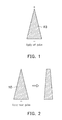
- FIG. 1 is a schematic diagram of a variable resistance element when a set pulse is applied to a resistive memory cell according to an embodiment of the invention.
- FIG. 2 is a schematic diagram of a variable resistance element when a set pulse and a reset pulse are applied to a resistive memory cell according to an embodiment of the invention.
- a resistive memory apparatus can apply a set pulse with a positive polarity to form a low resistance state to store data of, for example, logic 0.
- a reading current corresponding to different resistance state can be used to identify the resistance state thereof, so as to correctly read the data of logic 0.
- FIG. 1 and FIG. 2 can apply a set pulse with a positive polarity to form a low resistance state to store data of, for example, logic 0.
- a filament path of a variable resistance element 113 may have a sharp contour after the set pulse is applied thereto, such that a filament path with an excessively large width at one end and an excessively small width at another end is formed, which results in a problem of electromigration (EM).
- EM electromigration
- the control unit further provides a reset pulse to the resistive memory cell to change the contour of the variable resistance element 113, such that one end of the filament path with excessively small width can be broadened, so as to mitigate the problem of electromigration, as shown in FIG. 2 .
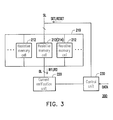
- FIG. 3 is a schematic diagram of a resistive memory apparatus according to an embodiment of the invention.
- the resistive memory apparatus 200 includes a resistive memory cell array 210, a current verification unit 220 and a control unit 230.
- the resistive memory cell array 210 includes a plurality of resistive memory cells 212.
- the resistive memory cell array 210 are coupled to the current verification unit 220 through a plurality of bit lines BL, and are coupled to the control unit 230 through a plurality of source lines SL.
- Each of the resistive memory cells 212 may include a switch element, for example, a metal oxide semiconductor field effective transistor (MOSFET) or a bipolar junction transistor, and a variable resistance element, and each of the resistive memory cells 212 can provide stored data of a single bit.
- a switch element for example, a metal oxide semiconductor field effective transistor (MOSFET) or a bipolar junction transistor, and a variable resistance element, and each of the resistive memory cells 212 can provide stored data of a single bit.
- the current verification unit 220 can be any type of a current measuring element/circuit, for example, a sensing amplifier circuit.
- the current verification unit 220 can be coupled to the resistive memory cells 212 through a plurality of the bit lines BL.
- the current verification unit 220 is configured to verify that reading currents generated by the resistive memory cells 212 are complied with a predetermined reference current when logic data is written into the resistive memory cells 212 to indicate that the control unit 230 correctly writes the logic data into the resistive memory cells 212.
- the control unit 230 is, for example, a central processing unit (CPU), a microprocessor, a digital signal processor (DSP), a programmable controller, a programmable logic device (PLD) or other similar devices or a combination of the above devices.
- the control unit is coupled to the current verification unit 220 and a plurality of the source lines SL of the resistive memory cell array 210. Detailed steps of a writing method of the resistive memory apparatus 200 are described below with reference of an embodiment.
- FIG. 4 is a flowchart illustrating a writing method of a resistive memory apparatus according to an embodiment of the invention.
- the method for writing logic data of the present embodiment is at least adapted to the resistive memory apparatus 200 of FIG. 3 , and detailed steps of the writing method of the present embodiment are described below with reference of various components in the resistive memory apparatus 200.
- step S410 the control unit 230 receives logic data DATA, and selects a corresponding resistive memory cell 212.
- the control unit 230 selects a corresponding resistive memory cell 214 from the resistive memory cells 212.
- the resistive memory cell 214 includes a switch element and a variable resistance element, for example, the variable resistance element 113 shown in FIG. 1 .
- the control unit 230 for example, provides a selecting voltage to a gate (or a base) of a transistor serving as the switch element in the resistive memory cell 214 to turn on the transistor, so as to perform a subsequent data writing operation to the resistive memory cell 214.
- step S420 the control unit 230 determines a logic level of the logic data DATA.
- the control unit 230 can determine the logic data DATA of the single bit to be in logic 1 or logic 0.
- step S430 the control unit 230 provides a reset pulse RESET to the resistive memory cell 214 during a writing period.
- the control unit 230 applies a reading voltage to the resistive memory cell 214, the resistive memory cell 214 generates a second reading current IR2 smaller than a second reference current, and outputs the same to the current verification unit 220 for verification.
- the control unit 230 provides the reset pulse RESET to the resistive memory cell 214 during the writing period when the second reading current IR2 is smaller than the second reference current.
- the control unit 230 if the second reading current IR2 generated by the resistive memory cell 214 does not pass through the verification of the current verification unit 220, the control unit 230, for example, further provides a set pulse SET to the resistive memory cell 214, such that the resistive memory cell 214 generates the second reading current IR2 smaller than the second reference current.
- the control unit 230 repeatedly and sequentially provides the reset pulse RESET and the set pulse SET to the resistive memory cell 214 during a reset operation period, such that the second reading current IR2 generate by the resistive memory cell 214 can pass through the verification of the current verification unit 220.
- step S440 the control unit 230 provides the set pulse SET and the reset pulse RESET to the resistive memory cell 214 during the writing period.
- the control unit 230 applies the reading voltage to the resistive memory cell 214, the resistive memory cell 214 generates a first reading current IR1 greater than a first reference current.
- the control unit 230 provides the set pulse SET and the reset pulse RESET to the resistive memory cell 214 during the writing period when the first reading current IR1 is greater than the first reference current.
- control unit 230 repeatedly and sequentially provides the set pulse SET and the reset pulse RESET to the resistive memory cell 214 during a set operation period, such that the first reading current IR1 generate by the resistive memory cell 214 can pass through the verification of the current verification unit 220. Therefore, according to the writing method of the present embodiment, during the writing period, by sequentially providing the set pulse SET and the reset pulse RESET to the resistive memory cell 214, the contour of the variable resistance element 113 can be changed, such that one end of the filament path with excessively small width therein can be broadened, so as to mitigate the problem of electromigration.
- the second reference current and the first reference current are, for example, determined by a reference current generated by applying the reading voltage to the resistive memory cell 214 with a resistance value of zero, and setting values of the second reference current and the first reference current can be the same or different, which is not limited by the invention.
- the reset pulse is, for example, a pulse with a negative polarity
- the set pulse is, for example, a pulse with a positive polarity, and polarities thereof are opposite.
- the control unit 230 writes the logic data DATA into the corresponding resistive memory cell 214 during the writing period.
- the current verification unit 220 verifies the reading current during the verification period, so as to ensure correctness of data writing. Therefore, the writing period of the present embodiment includes the verification period, and after the logic data DATA written into the resistive memory cell 214 is verified by the current verification unit 220, it represents that the data is successfully written to complete the writing operation.
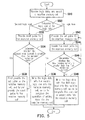
- FIG. 5 is a flowchart illustrating a writing method of a resistive memory apparatus according to another embodiment of the invention.
- the method writing logic data of the present embodiment is at least adapted to the resistive memory apparatus 200 of FIG. 3 , and detailed steps of the writing method of the present embodiment are described below with reference of various components in the resistive memory apparatus 200.
- step S510 the control unit 230 receives the logic data DATA, and selects the corresponding resistive memory cell 214.
- step S520 the control unit 230 determines the logic level of the logic data DATA.
- the steps S510 and S520 are the same or similar to the steps S410 and S420 of the embodiment of FIG. 4 , so that details thereof are not repeated.
- step S532 when the logic data DATA is in the logic 1 (i.e. the second logic level), in step S532, the control unit 230 provides the reset pulse RESET to the resistive memory cell 214.
- the current verification unit 220 determines whether the second reading current IR2 is greater than the second reference current. If not, i.e. the second reading current IR2 is smaller than or equal to the second reference current, it represents that the second reading current IR2 passes through the verification, and a step S536 is executed.
- the control unit 230 writes the logic data of the second logic level into the resistive memory cell 214 to complete the operation of writing data into the resistive memory cell 214.
- step S538 the control unit 230 first provides the set pulse SET to the resistive memory cell 214.
- the control unit 230 further provides the reset pulse RESET to the resistive memory cell 214 to make the second reading current IR2 to be smaller than or equal to the second reference current, such that the second reading current IR2 can pass through the verification of the current verification unit 220.
- the logic data writing method of the present embodiment repeatedly executes the step S534 and the step S536, such that the current verification unit 220 determines whether the second reading current IR2 is greater than the second reference current, and the control unit 230 provides the set pulse SET and the reset pulse RESET to the resistive memory cell 214 until the second reading current IR2 is smaller than or equal to the second reference current to pass through the verification of the current verification unit 220.
- the control unit 230 repeatedly and sequentially provides the reset pulse RESET and the set pulse SET to the resistive memory cell 214 during the reset operation period, such that the second reading current IR2 generate by the resistive memory cell 214 can pass through the verification of the current verification unit 220.
- the control unit 230 after providing the set pulse SET to the resistive memory cell 214, the control unit 230 further provides the reset pulse RESET to the resistive memory cell 214 to mitigate the problem of electromigration.
- step S542 when the logic data DATA is in logic 0 (i.e. the first logic level), in step S542, the control unit 230 first provides the set pulse SET to the resistive memory cell 214. In order to mitigate the problem of electromigration, in step S544, after providing the set pulse SET to the resistive memory cell 214, the control unit 230 further provides the reset pulse RESET to the resistive memory cell 214. Then, in step S546, the current verification unit 220 determines whether the first reading current IR1 is smaller than the first reference current. If not, i.e. the first reading current IR1 is greater than or equal to the second reference current, it represents that the first reading current IR1 passes through the verification, and a step S548 is executed. In the step S548, the control unit 230 writes the logic data with the first logic level into the resistive memory cell 214 to complete the operation of writing data into the resistive memory cell 214.
- the method flow returns to the step S542, by which the control unit 230 again provides the set pulse SET to the resistive memory cell 214.
- the logic data writing method of the present embodiment repeatedly executes the step S542 to the step S546, such that the control unit 230 provides the set pulse SET and the reset pulse RESET to the resistive memory cell 214, and the current verification unit 220 determines whether the first reading current IR1 is smaller than the first reference current until the first reading current IR1 is greater than or equal to the first reference current to pass through the verification of the current verification unit 220.
- the control unit 230 repeatedly and sequentially provides the set pulse SET and the reset pulse RESET to the resistive memory cell 214 during the set operation period, such that the first reading current IR1 generate by the resistive memory cell 214 can pass through the verification of the current verification unit 220. Moreover, in the step S542 and the step S544, after providing the set pulse SET to the resistive memory cell 214, the control unit 230 further provides the reset pulse RESET to the resistive memory cell 214 to mitigate the problem of electromigration.
- the control unit during the reset operation period, the control unit repeatedly and sequentially provides the reset pulse and the set pulse to the resistive memory cell.
- the control unit during the set operation period, the control unit repeatedly and sequentially provides the set pulse and the reset pulse to the resistive memory cell. Therefore, after providing the set pulse to the resistive memory cell, the control unit further provides the reset pulse to the resistive memory cell, so as to avoid excessive narrowing of the filament path in the variable resistance element to cause the problem of electromigration. Therefore, the resistive memory apparatus and the writing method thereof provided by the exemplary embodiments of the invention can correct write data.
Landscapes
- Semiconductor Memories (AREA)
- Read Only Memory (AREA)
- Mram Or Spin Memory Techniques (AREA)
Abstract
Description
- The invention relates to a memory apparatus and a writing method thereof, and particularly relates to a resistive memory apparatus and a writing method thereof.
- A non-volatile memory has an advantage that data stored therein is not disappeared after power off, so that it serves as a necessary memory element for maintaining a normal operation of many electronic products. Presently, a resistive random access memory (RRAM) is a kind of non-volatile memory positively developed in the industry, which has advantages of low write operation voltage, short write and erase time, long memory time, non-destructive reading, multi-state memory, simple structure and small occupation area, etc., and has a great application potential in personal computers and electronic equipment in the future.
- Generally, the resistive random access memory can change a width of a filament path according to magnitude and polarity of an applied pulse voltage, so as to set a resistance value to a low resistance state (LRS) or a high resistance state (HRS) in a reversible and non-volatile manner to respectively represent stored data of different logic levels. For example, when data of logic 1 is written, a reset pulse can be applied to narrow the width of the filament path to achieve the HRS. When data of logic 0 is written, a set pulse with an opposite polarity can be applied to broaden the width of the filament path to achieve the LRS. In this way, when the data is read, the data of logic 1 or logic 0 can be read according to a reading current of a different magnitude generated under different resistance states.
- However, when the data of logic 0 is written, the filament path in a variable resistance element may have a sharp contour after the set pulse is applied thereto, such that a filament path with an excessively large width at one end and an excessively small width at another end is formed, which results in a problem of electromigration (EM). To be specific, when a large current continuously flows through the variable resistance element, the narrower a place in the filament path is, the higher a current density at the place is, and the higher an electric field thereof is, which leads to a phenomenon that metal atoms move towards an electron flowing direction along grain boundaries of the variable resistance element itself. As the electromigration is continuously increased, the current density is accordingly increased to aggravate the situation. If the electromigration is too severe, the variable resistance element can be broken to form an open circuit, such that data cannot be correctly written.
- The invention is directed to a resistive memory apparatus and a writing method thereof, by which data is able to be correctly written.
- The invention provides a writing method of a resistive memory apparatus, which includes following steps. Logic data is received, and a corresponding resistive memory cell is selected. A logic level of the logic data is determined. When the logic data is in a first logic level, where a first reading current of the corresponding resistive memory cell is greater than a first reference current, a set pulse and a reset pulse are provided to the resistive memory cell during a writing period. Polarities of the reset pulse and the set pulse are opposite. When the logic data is in a second logic level, the reset pulse is typically provided to the resistive memory cell during the writing period, so as to generate a second reading current smaller than a second reference current when a reading voltage is applied to the resistive memory cell during a verification period. In case the reset pulse fails to generate the second reading current smaller than the second reference current, the set pulse is applied before re-applying the reset pulse.
- The invention provides a resistive memory apparatus including a resistive memory cell array, a current verification unit and a control unit. The resistive memory cell array includes a plurality of resistive memory cells. The control unit is coupled to the resistive memory cell array. The control unit receives logic data, and selects a corresponding resistive memory cell from the resistive memory cells. The control unit determines a logic level of the logic data. When the logic data is in a first logic level, where a first reading current is greater than a first reference current, the control unit provides a set pulse and a reset pulse to the resistive memory cell during a writing period. Polarities of the reset pulse and the set pulse are opposite.
- According to the above descriptions, in the exemplary embodiments of the invention, during the writing period, after the control unit provides the set pulse to the resistive memory cell, the control unit further provides the reset pulse to the resistive memory cell, so as to avoid the problem of electromigration caused by excessive narrow width of the filament path in the variable resistance element.
- In order to make the aforementioned and other features and advantages of the invention comprehensible, several exemplary embodiments accompanied with figures are described in detail below.
- The accompanying drawings are included to provide a further understanding of the invention, and are incorporated in and constitute a part of this specification. The drawings illustrate embodiments of the invention and, together with the description, serve to explain the principles of the invention.
-
FIG. 1 is a schematic diagram of a variable resistance element when a set pulse is applied to a resistive memory cell according to an embodiment of the invention. -
FIG. 2 is a schematic diagram of a variable resistance element when a set pulse and a reset pulse are applied to a resistive memory cell according to an embodiment of the invention. -
FIG. 3 is a schematic diagram of a resistive memory apparatus according to an embodiment of the invention. -
FIG. 4 is a flowchart illustrating a writing method of a resistive memory apparatus according to an embodiment of the invention. -
FIG. 5 is a flowchart illustrating a writing method of a resistive memory apparatus according to another embodiment of the invention. -
FIG. 1 is a schematic diagram of a variable resistance element when a set pulse is applied to a resistive memory cell according to an embodiment of the invention. -
FIG. 2 is a schematic diagram of a variable resistance element when a set pulse and a reset pulse are applied to a resistive memory cell according to an embodiment of the invention. Referring toFIG. 1 and FIG. 2 , during a writing period, a resistive memory apparatus can apply a set pulse with a positive polarity to form a low resistance state to store data of, for example, logic 0. When the data is read, a reading current corresponding to different resistance state can be used to identify the resistance state thereof, so as to correctly read the data of logic 0. However, according toFIG. 1 , it is known that when the data of logic 0 is written, a filament path of avariable resistance element 113 may have a sharp contour after the set pulse is applied thereto, such that a filament path with an excessively large width at one end and an excessively small width at another end is formed, which results in a problem of electromigration (EM). In an other embodiment of the invention, after a control unit provides the set pulse to the resistive memory cell, the control unit further provides a reset pulse to the resistive memory cell to change the contour of thevariable resistance element 113, such that one end of the filament path with excessively small width can be broadened, so as to mitigate the problem of electromigration, as shown inFIG. 2 . - Implementation of the resistive memory apparatus and a writing method thereof of the invention are described below.
-
FIG. 3 is a schematic diagram of a resistive memory apparatus according to an embodiment of the invention. Referring toFIG. 3 , theresistive memory apparatus 200 includes a resistivememory cell array 210, acurrent verification unit 220 and acontrol unit 230. The resistivememory cell array 210 includes a plurality ofresistive memory cells 212. The resistivememory cell array 210 are coupled to thecurrent verification unit 220 through a plurality of bit lines BL, and are coupled to thecontrol unit 230 through a plurality of source lines SL. Each of theresistive memory cells 212 may include a switch element, for example, a metal oxide semiconductor field effective transistor (MOSFET) or a bipolar junction transistor, and a variable resistance element, and each of theresistive memory cells 212 can provide stored data of a single bit. - The
current verification unit 220 can be any type of a current measuring element/circuit, for example, a sensing amplifier circuit. Thecurrent verification unit 220 can be coupled to theresistive memory cells 212 through a plurality of the bit lines BL. Thecurrent verification unit 220 is configured to verify that reading currents generated by theresistive memory cells 212 are complied with a predetermined reference current when logic data is written into theresistive memory cells 212 to indicate that thecontrol unit 230 correctly writes the logic data into theresistive memory cells 212. - The
control unit 230 is, for example, a central processing unit (CPU), a microprocessor, a digital signal processor (DSP), a programmable controller, a programmable logic device (PLD) or other similar devices or a combination of the above devices. The control unit is coupled to thecurrent verification unit 220 and a plurality of the source lines SL of the resistivememory cell array 210. Detailed steps of a writing method of theresistive memory apparatus 200 are described below with reference of an embodiment. -
FIG. 4 is a flowchart illustrating a writing method of a resistive memory apparatus according to an embodiment of the invention. Referring toFIG. 3 andFIG. 4 , the method for writing logic data of the present embodiment is at least adapted to theresistive memory apparatus 200 ofFIG. 3 , and detailed steps of the writing method of the present embodiment are described below with reference of various components in theresistive memory apparatus 200. - In step S410, the
control unit 230 receives logic data DATA, and selects a correspondingresistive memory cell 212. To be specific, when thecontrol unit 230 receives the logic data DATA of a single bit, thecontrol unit 230 selects a correspondingresistive memory cell 214 from theresistive memory cells 212. In the present embodiment, theresistive memory cell 214 includes a switch element and a variable resistance element, for example, thevariable resistance element 113 shown inFIG. 1 . Thecontrol unit 230, for example, provides a selecting voltage to a gate (or a base) of a transistor serving as the switch element in theresistive memory cell 214 to turn on the transistor, so as to perform a subsequent data writing operation to theresistive memory cell 214. - In step S420, the
control unit 230 determines a logic level of the logic data DATA. To be specific, thecontrol unit 230 can determine the logic data DATA of the single bit to be in logic 1 or logic 0. - When the logic data DATA is in logic 1 (i.e. a second logic level), in step S430, the
control unit 230 provides a reset pulse RESET to theresistive memory cell 214 during a writing period. During a verification period, when thecontrol unit 230 applies a reading voltage to theresistive memory cell 214, theresistive memory cell 214 generates a second reading current IR2 smaller than a second reference current, and outputs the same to thecurrent verification unit 220 for verification. In other words, thecontrol unit 230 provides the reset pulse RESET to theresistive memory cell 214 during the writing period when the second reading current IR2 is smaller than the second reference current. In an embodiment, if the second reading current IR2 generated by theresistive memory cell 214 does not pass through the verification of thecurrent verification unit 220, thecontrol unit 230, for example, further provides a set pulse SET to theresistive memory cell 214, such that theresistive memory cell 214 generates the second reading current IR2 smaller than the second reference current. In the present embodiment, thecontrol unit 230 repeatedly and sequentially provides the reset pulse RESET and the set pulse SET to theresistive memory cell 214 during a reset operation period, such that the second reading current IR2 generate by theresistive memory cell 214 can pass through the verification of thecurrent verification unit 220. - On the other hand, when the logic data DATA is in logic 0 (i.e. a first logic level), in step S440, the
control unit 230 provides the set pulse SET and the reset pulse RESET to theresistive memory cell 214 during the writing period. During the verification period, when thecontrol unit 230 applies the reading voltage to theresistive memory cell 214, theresistive memory cell 214 generates a first reading current IR1 greater than a first reference current. In other words, thecontrol unit 230 provides the set pulse SET and the reset pulse RESET to theresistive memory cell 214 during the writing period when the first reading current IR1 is greater than the first reference current. In the present embodiment, thecontrol unit 230 repeatedly and sequentially provides the set pulse SET and the reset pulse RESET to theresistive memory cell 214 during a set operation period, such that the first reading current IR1 generate by theresistive memory cell 214 can pass through the verification of thecurrent verification unit 220. Therefore, according to the writing method of the present embodiment, during the writing period, by sequentially providing the set pulse SET and the reset pulse RESET to theresistive memory cell 214, the contour of thevariable resistance element 113 can be changed, such that one end of the filament path with excessively small width therein can be broadened, so as to mitigate the problem of electromigration. - In the present embodiment, the second reference current and the first reference current are, for example, determined by a reference current generated by applying the reading voltage to the
resistive memory cell 214 with a resistance value of zero, and setting values of the second reference current and the first reference current can be the same or different, which is not limited by the invention. Moreover, in the present embodiment, the reset pulse is, for example, a pulse with a negative polarity, and the set pulse is, for example, a pulse with a positive polarity, and polarities thereof are opposite. - Moreover, in the present embodiment, the
control unit 230 writes the logic data DATA into the correspondingresistive memory cell 214 during the writing period. In the writing process, thecurrent verification unit 220 verifies the reading current during the verification period, so as to ensure correctness of data writing. Therefore, the writing period of the present embodiment includes the verification period, and after the logic data DATA written into theresistive memory cell 214 is verified by thecurrent verification unit 220, it represents that the data is successfully written to complete the writing operation. - In order to fully convey the spirit of the invention to those skilled in the art, another embodiment is provided below for further description.
-
FIG. 5 is a flowchart illustrating a writing method of a resistive memory apparatus according to another embodiment of the invention. Referring toFIG. 3 andFIG. 5 , the method writing logic data of the present embodiment is at least adapted to theresistive memory apparatus 200 ofFIG. 3 , and detailed steps of the writing method of the present embodiment are described below with reference of various components in theresistive memory apparatus 200. - In step S510, the
control unit 230 receives the logic data DATA, and selects the correspondingresistive memory cell 214. In step S520, thecontrol unit 230 determines the logic level of the logic data DATA. The steps S510 and S520 are the same or similar to the steps S410 and S420 of the embodiment ofFIG. 4 , so that details thereof are not repeated. - Then, in the present embodiment, when the logic data DATA is in the logic 1 (i.e. the second logic level), in step S532, the
control unit 230 provides the reset pulse RESET to theresistive memory cell 214. In step S534, thecurrent verification unit 220 determines whether the second reading current IR2 is greater than the second reference current. If not, i.e. the second reading current IR2 is smaller than or equal to the second reference current, it represents that the second reading current IR2 passes through the verification, and a step S536 is executed. In the step S536, thecontrol unit 230 writes the logic data of the second logic level into theresistive memory cell 214 to complete the operation of writing data into theresistive memory cell 214. - On the other hand, if the second reading current IR2 is greater than the second reference current, it represents that the second reading current IR2 does not pass through the verification, and a step S538 is executed. In the step S538, the
control unit 230 first provides the set pulse SET to theresistive memory cell 214. In order to mitigate the problem of electromigration, after providing the set pulse SET to theresistive memory cell 214, thecontrol unit 230 further provides the reset pulse RESET to theresistive memory cell 214 to make the second reading current IR2 to be smaller than or equal to the second reference current, such that the second reading current IR2 can pass through the verification of thecurrent verification unit 220. In other words, if the second reading current IR2 is greater than the second reference current, the logic data writing method of the present embodiment repeatedly executes the step S534 and the step S536, such that thecurrent verification unit 220 determines whether the second reading current IR2 is greater than the second reference current, and thecontrol unit 230 provides the set pulse SET and the reset pulse RESET to theresistive memory cell 214 until the second reading current IR2 is smaller than or equal to the second reference current to pass through the verification of thecurrent verification unit 220. - According to another aspect, in the step S532 to the step S536, the
control unit 230 repeatedly and sequentially provides the reset pulse RESET and the set pulse SET to theresistive memory cell 214 during the reset operation period, such that the second reading current IR2 generate by theresistive memory cell 214 can pass through the verification of thecurrent verification unit 220. Moreover, in the step S538, after providing the set pulse SET to theresistive memory cell 214, thecontrol unit 230 further provides the reset pulse RESET to theresistive memory cell 214 to mitigate the problem of electromigration. - Then, in the present embodiment, when the logic data DATA is in logic 0 (i.e. the first logic level), in step S542, the
control unit 230 first provides the set pulse SET to theresistive memory cell 214. In order to mitigate the problem of electromigration, in step S544, after providing the set pulse SET to theresistive memory cell 214, thecontrol unit 230 further provides the reset pulse RESET to theresistive memory cell 214. Then, in step S546, thecurrent verification unit 220 determines whether the first reading current IR1 is smaller than the first reference current. If not, i.e. the first reading current IR1 is greater than or equal to the second reference current, it represents that the first reading current IR1 passes through the verification, and a step S548 is executed. In the step S548, thecontrol unit 230 writes the logic data with the first logic level into theresistive memory cell 214 to complete the operation of writing data into theresistive memory cell 214. - On the other hand, if the generate first reading current IR1 is smaller than the first reference current, it represents that the first reading current IR1 does not pass through the verification, and the method flow returns to the step S542, by which the
control unit 230 again provides the set pulse SET to theresistive memory cell 214. In other words, if the first reading current IR1 is smaller than the first reference current, the logic data writing method of the present embodiment repeatedly executes the step S542 to the step S546, such that thecontrol unit 230 provides the set pulse SET and the reset pulse RESET to theresistive memory cell 214, and thecurrent verification unit 220 determines whether the first reading current IR1 is smaller than the first reference current until the first reading current IR1 is greater than or equal to the first reference current to pass through the verification of thecurrent verification unit 220. - Therefore, in the step S542 to the step S546, the
control unit 230 repeatedly and sequentially provides the set pulse SET and the reset pulse RESET to theresistive memory cell 214 during the set operation period, such that the first reading current IR1 generate by theresistive memory cell 214 can pass through the verification of thecurrent verification unit 220. Moreover, in the step S542 and the step S544, after providing the set pulse SET to theresistive memory cell 214, thecontrol unit 230 further provides the reset pulse RESET to theresistive memory cell 214 to mitigate the problem of electromigration. - Moreover, since those skilled in the art can learn enough instructions and recommendations for the writing method of the resistive memory apparatus of the present embodiment from the descriptions of the embodiments of
FIG. 1 to FIG. 4 , detailed description thereof is not repeated. - In summary, in the exemplary embodiment of the invention, during the reset operation period, the control unit repeatedly and sequentially provides the reset pulse and the set pulse to the resistive memory cell. Alternatively, during the set operation period, the control unit repeatedly and sequentially provides the set pulse and the reset pulse to the resistive memory cell. Therefore, after providing the set pulse to the resistive memory cell, the control unit further provides the reset pulse to the resistive memory cell, so as to avoid excessive narrowing of the filament path in the variable resistance element to cause the problem of electromigration. Therefore, the resistive memory apparatus and the writing method thereof provided by the exemplary embodiments of the invention can correct write data.
Claims (15)
- A writing method of a resistive memory apparatus (200), comprising:receiving logic data (DATA), and selecting a corresponding resistive memory cell (214);determining a logic level of the logic data (DATA);when the logic data (DATA) is in a first logic level, where a first reading current (IR1) of the corresponding resistive memory cell (214) is greater than a first reference current, providing a set pulse (SET) and a reset pulse (RESET) to the resistive memory cell (214) during a writing period, wherein polarities of the reset pulse (RESET) and the set pulse (SET) are opposite.
- The writing method of the resistive memory apparatus (200) as claimed in claim 1, wherein when the logic data (DATA) is in the first logic level, the step of providing the set pulse (SET) and the reset pulse (RESET) to the resistive memory cell (214) during the writing period comprises:providing the set pulse (SET) to the resistive memory cell (214); andproviding the reset pulse (RESET) to the resistive memory cell (214) after providing the set pulse (SET) to the resistive memory cell (214).
- The writing method of the resistive memory apparatus (200) as claimed in claim 2, wherein when the logic data (DATA) is in the first logic level, during the writing period, the writing method of the resistive memory apparatus (200) further comprises:determining whether the first reading current (IR1) is smaller than the first reference current; andproviding the set pulse (SET) and the reset pulse (RESET) to the resistive memory cell (214) when the first reading current (IR1) is smaller than the first reference current.
- The writing method of the resistive memory apparatus (200) as claimed in claim 3, wherein when the logic data (DATA) is in the first logic level, during the writing period, the writing method of the resistive memory apparatus (200) further comprises:writing the logic data (DATA) with the first logic level into the resistive memory cell (214) when the first reading current (IR1) is greater than or equal to the first reference current.
- The writing method of the resistive memory apparatus (200) as claimed in claim 3, wherein when the first reading current (IR1) is smaller than the first reference current, the step of determining whether the first reading current (IR1) is smaller than the first reference current and the step of providing the set pulse (SET) and the reset pulse (RESET) to the resistive memory cell (214) are repeatedly executed until the first reading current (IR1) is greater than or equal to the first reference current.
- The writing method of the resistive memory apparatus (200) as claimed in claim 1, further comprising:when the logic data (DATA) is in a second logic level, where a second reading current (IR2) of the resistive memory cell (214) is smaller than a second reference current, providing the reset pulse (RESET) to the resistive memory cell (214) during the writing period; andwhen the logic data (DATA) is in the second logic level, where the second reading current (IR2) greater is than the second reference current, further providing the set pulse (SET) to the resistive memory cell (214) during the writing period.
- The writing method of the resistive memory apparatus (200) as claimed in claim 6, wherein when the logic data (DATA) is in the second logic level, during the writing period, the writing method of the resistive memory apparatus (200) further comprises:determining whether the second reading current (IR2) is greater than the second reference current; andproviding the set pulse (SET) and the reset pulse (RESET) to the resistive memory cell (214) when the second reading current (IR2) is greater than the second reference current.
- A resistive memory apparatus (200), comprising:a resistive memory cell array (210), comprising a plurality of resistive memory cells (212); anda control unit (230), coupled to the resistive memory cell array (210), wherein the control unit (230) receives logic data (DATA); the control unit (230) selects a corresponding resistive memory cell (214) from the resistive memory cells (212); the control unit (230) determines a logic level of the logic data (DATA); and when the logic data (DATA) is in a first logic level, where a first reading current (IR1) of the corresponding resistive memory cell (214) is greater than a first reference current, the control unit (230) provides a set pulse (SET) and a reset pulse (RESET) to the resistive memory cell (214) during a writing period, wherein polarities of the reset pulse (RESET) and the set pulse (SET) are opposite.
- The resistive memory apparatus (200) as claimed in claim 8, wherein when the logic data (DATA) is in the first logic level, during the writing period, the control unit (230) provides the set pulse (SET) to the resistive memory cell (214), and provides the reset pulse (RESET) to the resistive memory cell (214) after providing the set pulse (SET) to the resistive memory cell (214).
- The resistive memory apparatus (200) as claimed in claim 9, wherein when the logic data (DATA) is in the first logic level, during the writing period, a current verification unit (220) determines whether the first reading current (IR1) is smaller than the first reference current, and when the first reading current (IR1) is smaller than the first reference current, the control unit (230) provides the set pulse (SET) and the reset pulse (RESET) to the resistive memory cell (214).
- The resistive memory apparatus (200) as claimed in claim 10, wherein when the logic data (DATA) is in the first logic level, during the writing period, when the first reading current (IR1) is greater than or equal to the first reference current, the control unit (230) writes the logic data (DATA) with the first logic level into the resistive memory cell (214).
- The resistive memory apparatus (200) as claimed in claim 10, wherein when the first reading current (IR1) is smaller than the first reference current, the current verification unit (220) determines whether the first reading current (IR1) is smaller than the first reference current, and the control unit (230) provides the set pulse (SET) and the reset pulse (RESET) to the resistive memory cell (214) until the first reading current (IR1) is greater than or equal to the first reference current.
- The resistive memory apparatus (200) as claimed in claim 8, wherein when the logic data (DATA) is in a second logic level, where a second reading current (IR2) of the resistive memory cell (214) smaller is than a second reference current, the control unit (230) provides a reset pulse (RESET) to the resistive memory cell (214) during a writing period; and when the logic data (DATA) is in the second logic level, where the second reading current (IR2) is greater than the second reference current, the control unit (230) further provides the set pulse (SET) to the resistive memory cell (214) during the writing period.
- The resistive memory apparatus (200) as claimed in claim 13, wherein when the logic data (DATA) is in the second logic level, during the writing period, a current verification unit (220) determines whether the second reading current (IR2) is greater than the second reference current, and when the second reading current (IR2) is greater than the second reference current, the control unit (230) provides the set pulse (SET) and the reset pulse (RESET) to the resistive memory cell (214).
- The resistive memory apparatus (200) as claimed in claim 14, wherein when the second reading current (IR2) is greater than the second reference current, the current verification unit (220) determines whether the second reading current (IR2) is greater than the second reference current, and the control unit (230) provides the set pulse (SET) and the reset pulse (RESET) to the resistive memory cell (214) until the second reading current (IR2) is smaller than or equal to the second reference current.
Applications Claiming Priority (1)
| Application Number | Priority Date | Filing Date | Title |
|---|---|---|---|
| US14/804,354 US9443587B1 (en) | 2015-07-21 | 2015-07-21 | Resistive memory apparatus and writing method thereof |
Publications (2)
| Publication Number | Publication Date |
|---|---|
| EP3121817A1 true EP3121817A1 (en) | 2017-01-25 |
| EP3121817B1 EP3121817B1 (en) | 2020-12-02 |
Family
ID=54360978
Family Applications (1)
| Application Number | Title | Priority Date | Filing Date |
|---|---|---|---|
| EP15192012.1A Active EP3121817B1 (en) | 2015-07-21 | 2015-10-29 | Resistive memory apparatus and writing method thereof |
Country Status (7)
| Country | Link |
|---|---|
| US (1) | US9443587B1 (en) |
| EP (1) | EP3121817B1 (en) |
| JP (1) | JP6088630B2 (en) |
| KR (1) | KR101689732B1 (en) |
| CN (1) | CN106373606B (en) |
| ES (1) | ES2854350T3 (en) |
| TW (1) | TWI571874B (en) |
Families Citing this family (15)
| Publication number | Priority date | Publication date | Assignee | Title |
|---|---|---|---|---|
| JP6830373B2 (en) | 2017-02-17 | 2021-02-17 | 株式会社日本製鋼所 | Parison separation device, hollow molding machine and manufacturing method of hollow molded products |
| JP6430576B2 (en) * | 2017-04-19 | 2018-11-28 | ウィンボンド エレクトロニクス コーポレーション | Resistance change random access memory |
| TWI657457B (en) * | 2017-06-27 | 2019-04-21 | 華邦電子股份有限公司 | Memory storage apparatus and method for testing memory storage apparatus |
| CN109147860B (en) | 2017-06-27 | 2020-11-17 | 华邦电子股份有限公司 | Memory storage device and test method thereof |
| CN109215709B (en) | 2017-07-03 | 2020-12-22 | 华邦电子股份有限公司 | Resistive memory device and setting method of resistive memory cell |
| CN110298203B (en) * | 2018-03-23 | 2023-06-23 | 华邦电子股份有限公司 | Key generation device and method |
| CN111554337B (en) * | 2019-02-11 | 2022-05-06 | 华邦电子股份有限公司 | Resistive memory and control method |
| CN110600068B (en) * | 2019-08-13 | 2021-06-04 | 中国科学院上海微系统与信息技术研究所 | A kind of staircase pulse determination method, system and storage medium |
| US10714157B1 (en) | 2019-08-27 | 2020-07-14 | Winbond Electronics Corp. | Non-volatile memory and reset method thereof |
| CN113012739B (en) * | 2019-12-20 | 2024-03-05 | 华邦电子股份有限公司 | Memory device and operation method thereof |
| US11362272B2 (en) | 2020-08-25 | 2022-06-14 | Winbond Electronics Corp. | Resistive memory device and reliability enhancement method thereof by using ratio of set current and reference current |
| TWI737465B (en) * | 2020-08-27 | 2021-08-21 | 華邦電子股份有限公司 | Resistive memory apparatus and operating method thereof |
| US11631809B2 (en) * | 2020-12-15 | 2023-04-18 | International Business Machines Corporation | In-memory resistive random access memory XOR logic using complimentary switching |
| US12596484B2 (en) | 2023-05-26 | 2026-04-07 | SanDisk Technologies, Inc. | Apparatus and method for two-step read of resistive random access memory |
| WO2026079301A1 (en) * | 2024-10-07 | 2026-04-16 | ヌヴォトンテクノロジージャパン株式会社 | Method for driving semiconductor device, and semiconductor device |
Citations (3)
| Publication number | Priority date | Publication date | Assignee | Title |
|---|---|---|---|---|
| US20100014343A1 (en) * | 2007-10-29 | 2010-01-21 | Zhiqiang Wei | Nonvolatile memory apparatus and nonvolatile data storage medium |
| EP2469541A1 (en) * | 2010-12-24 | 2012-06-27 | Samsung Electronics Co., Ltd. | Variable resistance device, semiconductor device including the variable resistance device, and method of operating the semiconductor device |
| US20130094275A1 (en) * | 2011-10-18 | 2013-04-18 | Micron Technology, Inc. | Stabilization of resistive memory |
Family Cites Families (14)
| Publication number | Priority date | Publication date | Assignee | Title |
|---|---|---|---|---|
| JP4742696B2 (en) * | 2005-06-27 | 2011-08-10 | ソニー株式会社 | Storage device |
| JP5095728B2 (en) * | 2007-03-13 | 2012-12-12 | パナソニック株式会社 | Resistance change type memory device |
| JP5253784B2 (en) * | 2007-10-17 | 2013-07-31 | 株式会社東芝 | Nonvolatile semiconductor memory device |
| CN102099863B (en) * | 2009-06-08 | 2014-04-02 | 松下电器产业株式会社 | Method of writing for resistance-change non-volatile memory element, and resistance-change non-volatile memory device |
| JP2013520761A (en) * | 2010-02-18 | 2013-06-06 | サンディスク スリーディー,エルエルシー | Step software program for reversible resistive switching devices |
| TWI446352B (en) | 2010-09-23 | 2014-07-21 | Ind Tech Res Inst | Resistive random access memory and verifying method thereof |
| KR20130021199A (en) * | 2011-08-22 | 2013-03-05 | 삼성전자주식회사 | Nonvolatile resistive memory device and method of driving the same |
| WO2013080499A1 (en) * | 2011-12-02 | 2013-06-06 | パナソニック株式会社 | Method of writing resistance change type nonvolatile storage element, and resistance change type nonvolatile storage device |
| TWI484490B (en) * | 2012-11-14 | 2015-05-11 | Univ Nat Chiao Tung | Resistive random access memory device and operating method thereof |
| KR102162701B1 (en) * | 2013-07-30 | 2020-10-07 | 에스케이하이닉스 주식회사 | Non-volatile memory apparatus and semiconductor system using the same |
| KR20150044475A (en) * | 2013-10-16 | 2015-04-27 | 에스케이하이닉스 주식회사 | Resistibility Memory Apparatus and Operation Method Thereof, and System Having the Same |
| TWI509614B (en) * | 2013-11-26 | 2015-11-21 | Winbond Electronics Corp | Resistive memory apparatus and write-in method thereof |
| US9000819B1 (en) * | 2013-12-18 | 2015-04-07 | Intermolecular, Inc. | Resistive switching schmitt triggers and comparators |
| KR102140788B1 (en) * | 2014-07-18 | 2020-08-03 | 삼성전자주식회사 | Resistive Memory Device and Operating Method thereof |
-
2015
- 2015-07-21 US US14/804,354 patent/US9443587B1/en active Active
- 2015-08-20 KR KR1020150117414A patent/KR101689732B1/en active Active
- 2015-10-13 TW TW104133523A patent/TWI571874B/en active
- 2015-10-13 CN CN201510669711.2A patent/CN106373606B/en active Active
- 2015-10-29 EP EP15192012.1A patent/EP3121817B1/en active Active
- 2015-10-29 ES ES15192012T patent/ES2854350T3/en active Active
- 2015-12-09 JP JP2015240122A patent/JP6088630B2/en active Active
Patent Citations (3)
| Publication number | Priority date | Publication date | Assignee | Title |
|---|---|---|---|---|
| US20100014343A1 (en) * | 2007-10-29 | 2010-01-21 | Zhiqiang Wei | Nonvolatile memory apparatus and nonvolatile data storage medium |
| EP2469541A1 (en) * | 2010-12-24 | 2012-06-27 | Samsung Electronics Co., Ltd. | Variable resistance device, semiconductor device including the variable resistance device, and method of operating the semiconductor device |
| US20130094275A1 (en) * | 2011-10-18 | 2013-04-18 | Micron Technology, Inc. | Stabilization of resistive memory |
Also Published As
| Publication number | Publication date |
|---|---|
| TW201705140A (en) | 2017-02-01 |
| CN106373606B (en) | 2019-02-01 |
| CN106373606A (en) | 2017-02-01 |
| TWI571874B (en) | 2017-02-21 |
| ES2854350T3 (en) | 2021-09-21 |
| JP6088630B2 (en) | 2017-03-01 |
| US9443587B1 (en) | 2016-09-13 |
| KR101689732B1 (en) | 2016-12-26 |
| EP3121817B1 (en) | 2020-12-02 |
| JP2017027648A (en) | 2017-02-02 |
Similar Documents
| Publication | Publication Date | Title |
|---|---|---|
| EP3121817B1 (en) | Resistive memory apparatus and writing method thereof | |
| US10991427B2 (en) | Memory programming methods and memory systems | |
| TWI571875B (en) | Resistive memory apparatus and a writing method thereof | |
| JP2023508514A (en) | Three-state programming of memory cells | |
| TWI543160B (en) | Resistance variable memory sensing | |
| CN109215729B (en) | Test apparatus for memory device and related test and manufacturing method for memory device | |
| CN110164496B (en) | Semiconductor memory device and method for reading the same | |
| TWI569271B (en) | Writing method for resistive memory apparatus | |
| US9715931B2 (en) | Resistive memory apparatus and a writing method thereof | |
| US10490297B2 (en) | Memory storage apparatus and method for testing memory storage apparatus | |
| EP3131096B1 (en) | Resistive memory apparatus and reading method thereof | |
| CN114514579A (en) | Voltage distribution for reducing read disturb in memory cells | |
| WO2017010991A1 (en) | Determining first write strength | |
| CN105304129B (en) | resistance variable memory and writing method thereof | |
| Cayo et al. | An Algorithmic Approach to the Design of a Comprehensive ReRAM Memory Controller | |
| CN109584930B (en) | Data reading method and nonvolatile memory device using the same | |
| EP4718457A1 (en) | Compute-in-memory arrays | |
| CN106328196A (en) | Writing method of resistive memory device | |
| TWI657457B (en) | Memory storage apparatus and method for testing memory storage apparatus | |
| TW201706997A (en) | Resistive memory apparatus and reading method thereof | |
| JP2017174486A (en) | Option code provision circuit and provision method thereof |
Legal Events
| Date | Code | Title | Description |
|---|---|---|---|
| PUAI | Public reference made under article 153(3) epc to a published international application that has entered the european phase |
Free format text: ORIGINAL CODE: 0009012 |
|
| STAA | Information on the status of an ep patent application or granted ep patent |
Free format text: STATUS: REQUEST FOR EXAMINATION WAS MADE |
|
| 17P | Request for examination filed |
Effective date: 20151029 |
|
| AK | Designated contracting states |
Kind code of ref document: A1 Designated state(s): AL AT BE BG CH CY CZ DE DK EE ES FI FR GB GR HR HU IE IS IT LI LT LU LV MC MK MT NL NO PL PT RO RS SE SI SK SM TR |
|
| AX | Request for extension of the european patent |
Extension state: BA ME |
|
| RBV | Designated contracting states (corrected) |
Designated state(s): AL AT BE BG CH CY CZ DE DK EE ES FI FR GB GR HR HU IE IS IT LI LT LU LV MC MK MT NL NO PL PT RO RS SE SI SK SM TR |
|
| GRAP | Despatch of communication of intention to grant a patent |
Free format text: ORIGINAL CODE: EPIDOSNIGR1 |
|
| STAA | Information on the status of an ep patent application or granted ep patent |
Free format text: STATUS: GRANT OF PATENT IS INTENDED |
|
| INTG | Intention to grant announced |
Effective date: 20200709 |
|
| GRAS | Grant fee paid |
Free format text: ORIGINAL CODE: EPIDOSNIGR3 |
|
| GRAA | (expected) grant |
Free format text: ORIGINAL CODE: 0009210 |
|
| STAA | Information on the status of an ep patent application or granted ep patent |
Free format text: STATUS: THE PATENT HAS BEEN GRANTED |
|
| AK | Designated contracting states |
Kind code of ref document: B1 Designated state(s): AL AT BE BG CH CY CZ DE DK EE ES FI FR GB GR HR HU IE IS IT LI LT LU LV MC MK MT NL NO PL PT RO RS SE SI SK SM TR |
|
| REG | Reference to a national code |
Ref country code: GB Ref legal event code: FG4D |
|
| REG | Reference to a national code |
Ref country code: AT Ref legal event code: REF Ref document number: 1341809 Country of ref document: AT Kind code of ref document: T Effective date: 20201215 Ref country code: CH Ref legal event code: EP |
|
| REG | Reference to a national code |
Ref country code: DE Ref legal event code: R096 Ref document number: 602015062832 Country of ref document: DE |
|
| REG | Reference to a national code |
Ref country code: IE Ref legal event code: FG4D |
|
| REG | Reference to a national code |
Ref country code: NL Ref legal event code: FP |
|
| PG25 | Lapsed in a contracting state [announced via postgrant information from national office to epo] |
Ref country code: FI Free format text: LAPSE BECAUSE OF FAILURE TO SUBMIT A TRANSLATION OF THE DESCRIPTION OR TO PAY THE FEE WITHIN THE PRESCRIBED TIME-LIMIT Effective date: 20201202 Ref country code: RS Free format text: LAPSE BECAUSE OF FAILURE TO SUBMIT A TRANSLATION OF THE DESCRIPTION OR TO PAY THE FEE WITHIN THE PRESCRIBED TIME-LIMIT Effective date: 20201202 Ref country code: NO Free format text: LAPSE BECAUSE OF FAILURE TO SUBMIT A TRANSLATION OF THE DESCRIPTION OR TO PAY THE FEE WITHIN THE PRESCRIBED TIME-LIMIT Effective date: 20210302 Ref country code: GR Free format text: LAPSE BECAUSE OF FAILURE TO SUBMIT A TRANSLATION OF THE DESCRIPTION OR TO PAY THE FEE WITHIN THE PRESCRIBED TIME-LIMIT Effective date: 20210303 |
|
| PG25 | Lapsed in a contracting state [announced via postgrant information from national office to epo] |
Ref country code: BG Free format text: LAPSE BECAUSE OF FAILURE TO SUBMIT A TRANSLATION OF THE DESCRIPTION OR TO PAY THE FEE WITHIN THE PRESCRIBED TIME-LIMIT Effective date: 20210302 Ref country code: LV Free format text: LAPSE BECAUSE OF FAILURE TO SUBMIT A TRANSLATION OF THE DESCRIPTION OR TO PAY THE FEE WITHIN THE PRESCRIBED TIME-LIMIT Effective date: 20201202 Ref country code: PL Free format text: LAPSE BECAUSE OF FAILURE TO SUBMIT A TRANSLATION OF THE DESCRIPTION OR TO PAY THE FEE WITHIN THE PRESCRIBED TIME-LIMIT Effective date: 20201202 Ref country code: SE Free format text: LAPSE BECAUSE OF FAILURE TO SUBMIT A TRANSLATION OF THE DESCRIPTION OR TO PAY THE FEE WITHIN THE PRESCRIBED TIME-LIMIT Effective date: 20201202 |
|
| PG25 | Lapsed in a contracting state [announced via postgrant information from national office to epo] |
Ref country code: HR Free format text: LAPSE BECAUSE OF FAILURE TO SUBMIT A TRANSLATION OF THE DESCRIPTION OR TO PAY THE FEE WITHIN THE PRESCRIBED TIME-LIMIT Effective date: 20201202 |
|
| REG | Reference to a national code |
Ref country code: LT Ref legal event code: MG9D |
|
| PG25 | Lapsed in a contracting state [announced via postgrant information from national office to epo] |
Ref country code: EE Free format text: LAPSE BECAUSE OF FAILURE TO SUBMIT A TRANSLATION OF THE DESCRIPTION OR TO PAY THE FEE WITHIN THE PRESCRIBED TIME-LIMIT Effective date: 20201202 Ref country code: CZ Free format text: LAPSE BECAUSE OF FAILURE TO SUBMIT A TRANSLATION OF THE DESCRIPTION OR TO PAY THE FEE WITHIN THE PRESCRIBED TIME-LIMIT Effective date: 20201202 Ref country code: SM Free format text: LAPSE BECAUSE OF FAILURE TO SUBMIT A TRANSLATION OF THE DESCRIPTION OR TO PAY THE FEE WITHIN THE PRESCRIBED TIME-LIMIT Effective date: 20201202 Ref country code: SK Free format text: LAPSE BECAUSE OF FAILURE TO SUBMIT A TRANSLATION OF THE DESCRIPTION OR TO PAY THE FEE WITHIN THE PRESCRIBED TIME-LIMIT Effective date: 20201202 Ref country code: RO Free format text: LAPSE BECAUSE OF FAILURE TO SUBMIT A TRANSLATION OF THE DESCRIPTION OR TO PAY THE FEE WITHIN THE PRESCRIBED TIME-LIMIT Effective date: 20201202 Ref country code: PT Free format text: LAPSE BECAUSE OF FAILURE TO SUBMIT A TRANSLATION OF THE DESCRIPTION OR TO PAY THE FEE WITHIN THE PRESCRIBED TIME-LIMIT Effective date: 20210405 Ref country code: LT Free format text: LAPSE BECAUSE OF FAILURE TO SUBMIT A TRANSLATION OF THE DESCRIPTION OR TO PAY THE FEE WITHIN THE PRESCRIBED TIME-LIMIT Effective date: 20201202 |
|
| REG | Reference to a national code |
Ref country code: DE Ref legal event code: R097 Ref document number: 602015062832 Country of ref document: DE |
|
| REG | Reference to a national code |
Ref country code: ES Ref legal event code: FG2A Ref document number: 2854350 Country of ref document: ES Kind code of ref document: T3 Effective date: 20210921 |
|
| PG25 | Lapsed in a contracting state [announced via postgrant information from national office to epo] |
Ref country code: IS Free format text: LAPSE BECAUSE OF FAILURE TO SUBMIT A TRANSLATION OF THE DESCRIPTION OR TO PAY THE FEE WITHIN THE PRESCRIBED TIME-LIMIT Effective date: 20210402 |
|
| PLBE | No opposition filed within time limit |
Free format text: ORIGINAL CODE: 0009261 |
|
| STAA | Information on the status of an ep patent application or granted ep patent |
Free format text: STATUS: NO OPPOSITION FILED WITHIN TIME LIMIT |
|
| PG25 | Lapsed in a contracting state [announced via postgrant information from national office to epo] |
Ref country code: IT Free format text: LAPSE BECAUSE OF FAILURE TO SUBMIT A TRANSLATION OF THE DESCRIPTION OR TO PAY THE FEE WITHIN THE PRESCRIBED TIME-LIMIT Effective date: 20201202 Ref country code: AL Free format text: LAPSE BECAUSE OF FAILURE TO SUBMIT A TRANSLATION OF THE DESCRIPTION OR TO PAY THE FEE WITHIN THE PRESCRIBED TIME-LIMIT Effective date: 20201202 |
|
| 26N | No opposition filed |
Effective date: 20210903 |
|
| PG25 | Lapsed in a contracting state [announced via postgrant information from national office to epo] |
Ref country code: SI Free format text: LAPSE BECAUSE OF FAILURE TO SUBMIT A TRANSLATION OF THE DESCRIPTION OR TO PAY THE FEE WITHIN THE PRESCRIBED TIME-LIMIT Effective date: 20201202 Ref country code: DK Free format text: LAPSE BECAUSE OF FAILURE TO SUBMIT A TRANSLATION OF THE DESCRIPTION OR TO PAY THE FEE WITHIN THE PRESCRIBED TIME-LIMIT Effective date: 20201202 |
|
| REG | Reference to a national code |
Ref country code: CH Ref legal event code: PL |
|
| PG25 | Lapsed in a contracting state [announced via postgrant information from national office to epo] |
Ref country code: IS Free format text: LAPSE BECAUSE OF FAILURE TO SUBMIT A TRANSLATION OF THE DESCRIPTION OR TO PAY THE FEE WITHIN THE PRESCRIBED TIME-LIMIT Effective date: 20210402 |
|
| REG | Reference to a national code |
Ref country code: BE Ref legal event code: MM Effective date: 20211031 |
|
| PG25 | Lapsed in a contracting state [announced via postgrant information from national office to epo] |
Ref country code: MC Free format text: LAPSE BECAUSE OF FAILURE TO SUBMIT A TRANSLATION OF THE DESCRIPTION OR TO PAY THE FEE WITHIN THE PRESCRIBED TIME-LIMIT Effective date: 20201202 |
|
| PG25 | Lapsed in a contracting state [announced via postgrant information from national office to epo] |
Ref country code: LU Free format text: LAPSE BECAUSE OF NON-PAYMENT OF DUE FEES Effective date: 20211029 Ref country code: BE Free format text: LAPSE BECAUSE OF NON-PAYMENT OF DUE FEES Effective date: 20211031 |
|
| PG25 | Lapsed in a contracting state [announced via postgrant information from national office to epo] |
Ref country code: LI Free format text: LAPSE BECAUSE OF NON-PAYMENT OF DUE FEES Effective date: 20211031 Ref country code: CH Free format text: LAPSE BECAUSE OF NON-PAYMENT OF DUE FEES Effective date: 20211031 |
|
| PG25 | Lapsed in a contracting state [announced via postgrant information from national office to epo] |
Ref country code: IE Free format text: LAPSE BECAUSE OF NON-PAYMENT OF DUE FEES Effective date: 20211029 |
|
| PG25 | Lapsed in a contracting state [announced via postgrant information from national office to epo] |
Ref country code: HU Free format text: LAPSE BECAUSE OF FAILURE TO SUBMIT A TRANSLATION OF THE DESCRIPTION OR TO PAY THE FEE WITHIN THE PRESCRIBED TIME-LIMIT; INVALID AB INITIO Effective date: 20151029 |
|
| PG25 | Lapsed in a contracting state [announced via postgrant information from national office to epo] |
Ref country code: CY Free format text: LAPSE BECAUSE OF FAILURE TO SUBMIT A TRANSLATION OF THE DESCRIPTION OR TO PAY THE FEE WITHIN THE PRESCRIBED TIME-LIMIT Effective date: 20201202 |
|
| PG25 | Lapsed in a contracting state [announced via postgrant information from national office to epo] |
Ref country code: MK Free format text: LAPSE BECAUSE OF FAILURE TO SUBMIT A TRANSLATION OF THE DESCRIPTION OR TO PAY THE FEE WITHIN THE PRESCRIBED TIME-LIMIT Effective date: 20201202 |
|
| PG25 | Lapsed in a contracting state [announced via postgrant information from national office to epo] |
Ref country code: MT Free format text: LAPSE BECAUSE OF FAILURE TO SUBMIT A TRANSLATION OF THE DESCRIPTION OR TO PAY THE FEE WITHIN THE PRESCRIBED TIME-LIMIT Effective date: 20201202 |
|
| PGFP | Annual fee paid to national office [announced via postgrant information from national office to epo] |
Ref country code: NL Payment date: 20251024 Year of fee payment: 11 |
|
| PG25 | Lapsed in a contracting state [announced via postgrant information from national office to epo] |
Ref country code: TR Free format text: LAPSE BECAUSE OF FAILURE TO SUBMIT A TRANSLATION OF THE DESCRIPTION OR TO PAY THE FEE WITHIN THE PRESCRIBED TIME-LIMIT Effective date: 20201202 |
|
| PGFP | Annual fee paid to national office [announced via postgrant information from national office to epo] |
Ref country code: DE Payment date: 20251028 Year of fee payment: 11 |
|
| PGFP | Annual fee paid to national office [announced via postgrant information from national office to epo] |
Ref country code: GB Payment date: 20251023 Year of fee payment: 11 |
|
| PGFP | Annual fee paid to national office [announced via postgrant information from national office to epo] |
Ref country code: AT Payment date: 20251020 Year of fee payment: 11 |
|
| PGFP | Annual fee paid to national office [announced via postgrant information from national office to epo] |
Ref country code: FR Payment date: 20251027 Year of fee payment: 11 |
|
| PGFP | Annual fee paid to national office [announced via postgrant information from national office to epo] |
Ref country code: ES Payment date: 20251118 Year of fee payment: 11 |