EP3121309A1 - Methods for depositing group 13 metal or metalloid nitride films - Google Patents
Methods for depositing group 13 metal or metalloid nitride films Download PDFInfo
- Publication number
- EP3121309A1 EP3121309A1 EP16181088.2A EP16181088A EP3121309A1 EP 3121309 A1 EP3121309 A1 EP 3121309A1 EP 16181088 A EP16181088 A EP 16181088A EP 3121309 A1 EP3121309 A1 EP 3121309A1
- Authority
- EP
- European Patent Office
- Prior art keywords
- plasma
- group
- reactor
- nitride
- aluminum
- Prior art date
- Legal status (The legal status is an assumption and is not a legal conclusion. Google has not performed a legal analysis and makes no representation as to the accuracy of the status listed.)
- Withdrawn
Links
Images





Classifications
-
- C—CHEMISTRY; METALLURGY
- C23—COATING METALLIC MATERIAL; COATING MATERIAL WITH METALLIC MATERIAL; CHEMICAL SURFACE TREATMENT; DIFFUSION TREATMENT OF METALLIC MATERIAL; COATING BY VACUUM EVAPORATION, BY SPUTTERING, BY ION IMPLANTATION OR BY CHEMICAL VAPOUR DEPOSITION, IN GENERAL; INHIBITING CORROSION OF METALLIC MATERIAL OR INCRUSTATION IN GENERAL
- C23C—COATING METALLIC MATERIAL; COATING MATERIAL WITH METALLIC MATERIAL; SURFACE TREATMENT OF METALLIC MATERIAL BY DIFFUSION INTO THE SURFACE, BY CHEMICAL CONVERSION OR SUBSTITUTION; COATING BY VACUUM EVAPORATION, BY SPUTTERING, BY ION IMPLANTATION OR BY CHEMICAL VAPOUR DEPOSITION, IN GENERAL
- C23C16/00—Chemical coating by decomposition of gaseous compounds, without leaving reaction products of surface material in the coating, i.e. chemical vapour deposition [CVD] processes
- C23C16/44—Chemical coating by decomposition of gaseous compounds, without leaving reaction products of surface material in the coating, i.e. chemical vapour deposition [CVD] processes characterised by the method of coating
- C23C16/50—Chemical coating by decomposition of gaseous compounds, without leaving reaction products of surface material in the coating, i.e. chemical vapour deposition [CVD] processes characterised by the method of coating using electric discharges
-
- H—ELECTRICITY
- H10—SEMICONDUCTOR DEVICES; ELECTRIC SOLID-STATE DEVICES NOT OTHERWISE PROVIDED FOR
- H10D—INORGANIC ELECTRIC SEMICONDUCTOR DEVICES
- H10D64/00—Electrodes of devices having potential barriers
- H10D64/01—Manufacture or treatment
- H10D64/013—Manufacture or treatment of electrodes having a conductor capacitively coupled to a semiconductor by an insulator
- H10D64/01302—Manufacture or treatment of electrodes having a conductor capacitively coupled to a semiconductor by an insulator the insulator being formed after the semiconductor body, the semiconductor being silicon
- H10D64/01332—Making the insulator
- H10D64/01336—Making the insulator on single crystalline silicon, e.g. chemical oxidation using a liquid
- H10D64/01344—Making the insulator on single crystalline silicon, e.g. chemical oxidation using a liquid in a nitrogen-containing ambient, e.g. N2O oxidation
-
- C—CHEMISTRY; METALLURGY
- C23—COATING METALLIC MATERIAL; COATING MATERIAL WITH METALLIC MATERIAL; CHEMICAL SURFACE TREATMENT; DIFFUSION TREATMENT OF METALLIC MATERIAL; COATING BY VACUUM EVAPORATION, BY SPUTTERING, BY ION IMPLANTATION OR BY CHEMICAL VAPOUR DEPOSITION, IN GENERAL; INHIBITING CORROSION OF METALLIC MATERIAL OR INCRUSTATION IN GENERAL
- C23C—COATING METALLIC MATERIAL; COATING MATERIAL WITH METALLIC MATERIAL; SURFACE TREATMENT OF METALLIC MATERIAL BY DIFFUSION INTO THE SURFACE, BY CHEMICAL CONVERSION OR SUBSTITUTION; COATING BY VACUUM EVAPORATION, BY SPUTTERING, BY ION IMPLANTATION OR BY CHEMICAL VAPOUR DEPOSITION, IN GENERAL
- C23C16/00—Chemical coating by decomposition of gaseous compounds, without leaving reaction products of surface material in the coating, i.e. chemical vapour deposition [CVD] processes
- C23C16/22—Chemical coating by decomposition of gaseous compounds, without leaving reaction products of surface material in the coating, i.e. chemical vapour deposition [CVD] processes characterised by the deposition of inorganic material, other than metallic material
- C23C16/30—Deposition of compounds, mixtures or solid solutions, e.g. borides, carbides, nitrides
- C23C16/301—AIII BV compounds, where A is Al, Ga, In or Tl and B is N, P, As, Sb or Bi
- C23C16/303—Nitrides
-
- C—CHEMISTRY; METALLURGY
- C23—COATING METALLIC MATERIAL; COATING MATERIAL WITH METALLIC MATERIAL; CHEMICAL SURFACE TREATMENT; DIFFUSION TREATMENT OF METALLIC MATERIAL; COATING BY VACUUM EVAPORATION, BY SPUTTERING, BY ION IMPLANTATION OR BY CHEMICAL VAPOUR DEPOSITION, IN GENERAL; INHIBITING CORROSION OF METALLIC MATERIAL OR INCRUSTATION IN GENERAL
- C23C—COATING METALLIC MATERIAL; COATING MATERIAL WITH METALLIC MATERIAL; SURFACE TREATMENT OF METALLIC MATERIAL BY DIFFUSION INTO THE SURFACE, BY CHEMICAL CONVERSION OR SUBSTITUTION; COATING BY VACUUM EVAPORATION, BY SPUTTERING, BY ION IMPLANTATION OR BY CHEMICAL VAPOUR DEPOSITION, IN GENERAL
- C23C16/00—Chemical coating by decomposition of gaseous compounds, without leaving reaction products of surface material in the coating, i.e. chemical vapour deposition [CVD] processes
- C23C16/22—Chemical coating by decomposition of gaseous compounds, without leaving reaction products of surface material in the coating, i.e. chemical vapour deposition [CVD] processes characterised by the deposition of inorganic material, other than metallic material
- C23C16/30—Deposition of compounds, mixtures or solid solutions, e.g. borides, carbides, nitrides
- C23C16/34—Nitrides
-
- C—CHEMISTRY; METALLURGY
- C23—COATING METALLIC MATERIAL; COATING MATERIAL WITH METALLIC MATERIAL; CHEMICAL SURFACE TREATMENT; DIFFUSION TREATMENT OF METALLIC MATERIAL; COATING BY VACUUM EVAPORATION, BY SPUTTERING, BY ION IMPLANTATION OR BY CHEMICAL VAPOUR DEPOSITION, IN GENERAL; INHIBITING CORROSION OF METALLIC MATERIAL OR INCRUSTATION IN GENERAL
- C23C—COATING METALLIC MATERIAL; COATING MATERIAL WITH METALLIC MATERIAL; SURFACE TREATMENT OF METALLIC MATERIAL BY DIFFUSION INTO THE SURFACE, BY CHEMICAL CONVERSION OR SUBSTITUTION; COATING BY VACUUM EVAPORATION, BY SPUTTERING, BY ION IMPLANTATION OR BY CHEMICAL VAPOUR DEPOSITION, IN GENERAL
- C23C16/00—Chemical coating by decomposition of gaseous compounds, without leaving reaction products of surface material in the coating, i.e. chemical vapour deposition [CVD] processes
- C23C16/22—Chemical coating by decomposition of gaseous compounds, without leaving reaction products of surface material in the coating, i.e. chemical vapour deposition [CVD] processes characterised by the deposition of inorganic material, other than metallic material
- C23C16/30—Deposition of compounds, mixtures or solid solutions, e.g. borides, carbides, nitrides
- C23C16/34—Nitrides
- C23C16/342—Boron nitride
-
- C—CHEMISTRY; METALLURGY
- C23—COATING METALLIC MATERIAL; COATING MATERIAL WITH METALLIC MATERIAL; CHEMICAL SURFACE TREATMENT; DIFFUSION TREATMENT OF METALLIC MATERIAL; COATING BY VACUUM EVAPORATION, BY SPUTTERING, BY ION IMPLANTATION OR BY CHEMICAL VAPOUR DEPOSITION, IN GENERAL; INHIBITING CORROSION OF METALLIC MATERIAL OR INCRUSTATION IN GENERAL
- C23C—COATING METALLIC MATERIAL; COATING MATERIAL WITH METALLIC MATERIAL; SURFACE TREATMENT OF METALLIC MATERIAL BY DIFFUSION INTO THE SURFACE, BY CHEMICAL CONVERSION OR SUBSTITUTION; COATING BY VACUUM EVAPORATION, BY SPUTTERING, BY ION IMPLANTATION OR BY CHEMICAL VAPOUR DEPOSITION, IN GENERAL
- C23C16/00—Chemical coating by decomposition of gaseous compounds, without leaving reaction products of surface material in the coating, i.e. chemical vapour deposition [CVD] processes
- C23C16/44—Chemical coating by decomposition of gaseous compounds, without leaving reaction products of surface material in the coating, i.e. chemical vapour deposition [CVD] processes characterised by the method of coating
- C23C16/4401—Means for minimising impurities, e.g. dust, moisture or residual gas, in the reaction chamber
- C23C16/4408—Means for minimising impurities, e.g. dust, moisture or residual gas, in the reaction chamber by purging residual gases from the reaction chamber or gas lines
-
- C—CHEMISTRY; METALLURGY
- C23—COATING METALLIC MATERIAL; COATING MATERIAL WITH METALLIC MATERIAL; CHEMICAL SURFACE TREATMENT; DIFFUSION TREATMENT OF METALLIC MATERIAL; COATING BY VACUUM EVAPORATION, BY SPUTTERING, BY ION IMPLANTATION OR BY CHEMICAL VAPOUR DEPOSITION, IN GENERAL; INHIBITING CORROSION OF METALLIC MATERIAL OR INCRUSTATION IN GENERAL
- C23C—COATING METALLIC MATERIAL; COATING MATERIAL WITH METALLIC MATERIAL; SURFACE TREATMENT OF METALLIC MATERIAL BY DIFFUSION INTO THE SURFACE, BY CHEMICAL CONVERSION OR SUBSTITUTION; COATING BY VACUUM EVAPORATION, BY SPUTTERING, BY ION IMPLANTATION OR BY CHEMICAL VAPOUR DEPOSITION, IN GENERAL
- C23C16/00—Chemical coating by decomposition of gaseous compounds, without leaving reaction products of surface material in the coating, i.e. chemical vapour deposition [CVD] processes
- C23C16/44—Chemical coating by decomposition of gaseous compounds, without leaving reaction products of surface material in the coating, i.e. chemical vapour deposition [CVD] processes characterised by the method of coating
- C23C16/455—Chemical coating by decomposition of gaseous compounds, without leaving reaction products of surface material in the coating, i.e. chemical vapour deposition [CVD] processes characterised by the method of coating characterised by the method used for introducing gases into reaction chamber or for modifying gas flows in reaction chamber
-
- C—CHEMISTRY; METALLURGY
- C23—COATING METALLIC MATERIAL; COATING MATERIAL WITH METALLIC MATERIAL; CHEMICAL SURFACE TREATMENT; DIFFUSION TREATMENT OF METALLIC MATERIAL; COATING BY VACUUM EVAPORATION, BY SPUTTERING, BY ION IMPLANTATION OR BY CHEMICAL VAPOUR DEPOSITION, IN GENERAL; INHIBITING CORROSION OF METALLIC MATERIAL OR INCRUSTATION IN GENERAL
- C23C—COATING METALLIC MATERIAL; COATING MATERIAL WITH METALLIC MATERIAL; SURFACE TREATMENT OF METALLIC MATERIAL BY DIFFUSION INTO THE SURFACE, BY CHEMICAL CONVERSION OR SUBSTITUTION; COATING BY VACUUM EVAPORATION, BY SPUTTERING, BY ION IMPLANTATION OR BY CHEMICAL VAPOUR DEPOSITION, IN GENERAL
- C23C16/00—Chemical coating by decomposition of gaseous compounds, without leaving reaction products of surface material in the coating, i.e. chemical vapour deposition [CVD] processes
- C23C16/44—Chemical coating by decomposition of gaseous compounds, without leaving reaction products of surface material in the coating, i.e. chemical vapour deposition [CVD] processes characterised by the method of coating
- C23C16/455—Chemical coating by decomposition of gaseous compounds, without leaving reaction products of surface material in the coating, i.e. chemical vapour deposition [CVD] processes characterised by the method of coating characterised by the method used for introducing gases into reaction chamber or for modifying gas flows in reaction chamber
- C23C16/45523—Pulsed gas flow or change of composition over time
- C23C16/45525—Atomic layer deposition [ALD]
-
- C—CHEMISTRY; METALLURGY
- C23—COATING METALLIC MATERIAL; COATING MATERIAL WITH METALLIC MATERIAL; CHEMICAL SURFACE TREATMENT; DIFFUSION TREATMENT OF METALLIC MATERIAL; COATING BY VACUUM EVAPORATION, BY SPUTTERING, BY ION IMPLANTATION OR BY CHEMICAL VAPOUR DEPOSITION, IN GENERAL; INHIBITING CORROSION OF METALLIC MATERIAL OR INCRUSTATION IN GENERAL
- C23C—COATING METALLIC MATERIAL; COATING MATERIAL WITH METALLIC MATERIAL; SURFACE TREATMENT OF METALLIC MATERIAL BY DIFFUSION INTO THE SURFACE, BY CHEMICAL CONVERSION OR SUBSTITUTION; COATING BY VACUUM EVAPORATION, BY SPUTTERING, BY ION IMPLANTATION OR BY CHEMICAL VAPOUR DEPOSITION, IN GENERAL
- C23C16/00—Chemical coating by decomposition of gaseous compounds, without leaving reaction products of surface material in the coating, i.e. chemical vapour deposition [CVD] processes
- C23C16/44—Chemical coating by decomposition of gaseous compounds, without leaving reaction products of surface material in the coating, i.e. chemical vapour deposition [CVD] processes characterised by the method of coating
- C23C16/455—Chemical coating by decomposition of gaseous compounds, without leaving reaction products of surface material in the coating, i.e. chemical vapour deposition [CVD] processes characterised by the method of coating characterised by the method used for introducing gases into reaction chamber or for modifying gas flows in reaction chamber
- C23C16/45523—Pulsed gas flow or change of composition over time
- C23C16/45525—Atomic layer deposition [ALD]
- C23C16/45527—Atomic layer deposition [ALD] characterized by the ALD cycle, e.g. different flows or temperatures during half-reactions, unusual pulsing sequence, use of precursor mixtures or auxiliary reactants or activations
- C23C16/45531—Atomic layer deposition [ALD] characterized by the ALD cycle, e.g. different flows or temperatures during half-reactions, unusual pulsing sequence, use of precursor mixtures or auxiliary reactants or activations specially adapted for making ternary or higher compositions
-
- C—CHEMISTRY; METALLURGY
- C23—COATING METALLIC MATERIAL; COATING MATERIAL WITH METALLIC MATERIAL; CHEMICAL SURFACE TREATMENT; DIFFUSION TREATMENT OF METALLIC MATERIAL; COATING BY VACUUM EVAPORATION, BY SPUTTERING, BY ION IMPLANTATION OR BY CHEMICAL VAPOUR DEPOSITION, IN GENERAL; INHIBITING CORROSION OF METALLIC MATERIAL OR INCRUSTATION IN GENERAL
- C23C—COATING METALLIC MATERIAL; COATING MATERIAL WITH METALLIC MATERIAL; SURFACE TREATMENT OF METALLIC MATERIAL BY DIFFUSION INTO THE SURFACE, BY CHEMICAL CONVERSION OR SUBSTITUTION; COATING BY VACUUM EVAPORATION, BY SPUTTERING, BY ION IMPLANTATION OR BY CHEMICAL VAPOUR DEPOSITION, IN GENERAL
- C23C16/00—Chemical coating by decomposition of gaseous compounds, without leaving reaction products of surface material in the coating, i.e. chemical vapour deposition [CVD] processes
- C23C16/44—Chemical coating by decomposition of gaseous compounds, without leaving reaction products of surface material in the coating, i.e. chemical vapour deposition [CVD] processes characterised by the method of coating
- C23C16/455—Chemical coating by decomposition of gaseous compounds, without leaving reaction products of surface material in the coating, i.e. chemical vapour deposition [CVD] processes characterised by the method of coating characterised by the method used for introducing gases into reaction chamber or for modifying gas flows in reaction chamber
- C23C16/45523—Pulsed gas flow or change of composition over time
- C23C16/45525—Atomic layer deposition [ALD]
- C23C16/45527—Atomic layer deposition [ALD] characterized by the ALD cycle, e.g. different flows or temperatures during half-reactions, unusual pulsing sequence, use of precursor mixtures or auxiliary reactants or activations
- C23C16/45536—Use of plasma, radiation or electromagnetic fields
- C23C16/45542—Plasma being used non-continuously during the ALD reactions
-
- C—CHEMISTRY; METALLURGY
- C23—COATING METALLIC MATERIAL; COATING MATERIAL WITH METALLIC MATERIAL; CHEMICAL SURFACE TREATMENT; DIFFUSION TREATMENT OF METALLIC MATERIAL; COATING BY VACUUM EVAPORATION, BY SPUTTERING, BY ION IMPLANTATION OR BY CHEMICAL VAPOUR DEPOSITION, IN GENERAL; INHIBITING CORROSION OF METALLIC MATERIAL OR INCRUSTATION IN GENERAL
- C23C—COATING METALLIC MATERIAL; COATING MATERIAL WITH METALLIC MATERIAL; SURFACE TREATMENT OF METALLIC MATERIAL BY DIFFUSION INTO THE SURFACE, BY CHEMICAL CONVERSION OR SUBSTITUTION; COATING BY VACUUM EVAPORATION, BY SPUTTERING, BY ION IMPLANTATION OR BY CHEMICAL VAPOUR DEPOSITION, IN GENERAL
- C23C16/00—Chemical coating by decomposition of gaseous compounds, without leaving reaction products of surface material in the coating, i.e. chemical vapour deposition [CVD] processes
- C23C16/44—Chemical coating by decomposition of gaseous compounds, without leaving reaction products of surface material in the coating, i.e. chemical vapour deposition [CVD] processes characterised by the method of coating
- C23C16/455—Chemical coating by decomposition of gaseous compounds, without leaving reaction products of surface material in the coating, i.e. chemical vapour deposition [CVD] processes characterised by the method of coating characterised by the method used for introducing gases into reaction chamber or for modifying gas flows in reaction chamber
- C23C16/45523—Pulsed gas flow or change of composition over time
- C23C16/45525—Atomic layer deposition [ALD]
- C23C16/45553—Atomic layer deposition [ALD] characterized by the use of precursors specially adapted for ALD
-
- C—CHEMISTRY; METALLURGY
- C23—COATING METALLIC MATERIAL; COATING MATERIAL WITH METALLIC MATERIAL; CHEMICAL SURFACE TREATMENT; DIFFUSION TREATMENT OF METALLIC MATERIAL; COATING BY VACUUM EVAPORATION, BY SPUTTERING, BY ION IMPLANTATION OR BY CHEMICAL VAPOUR DEPOSITION, IN GENERAL; INHIBITING CORROSION OF METALLIC MATERIAL OR INCRUSTATION IN GENERAL
- C23C—COATING METALLIC MATERIAL; COATING MATERIAL WITH METALLIC MATERIAL; SURFACE TREATMENT OF METALLIC MATERIAL BY DIFFUSION INTO THE SURFACE, BY CHEMICAL CONVERSION OR SUBSTITUTION; COATING BY VACUUM EVAPORATION, BY SPUTTERING, BY ION IMPLANTATION OR BY CHEMICAL VAPOUR DEPOSITION, IN GENERAL
- C23C16/00—Chemical coating by decomposition of gaseous compounds, without leaving reaction products of surface material in the coating, i.e. chemical vapour deposition [CVD] processes
- C23C16/44—Chemical coating by decomposition of gaseous compounds, without leaving reaction products of surface material in the coating, i.e. chemical vapour deposition [CVD] processes characterised by the method of coating
- C23C16/48—Chemical coating by decomposition of gaseous compounds, without leaving reaction products of surface material in the coating, i.e. chemical vapour deposition [CVD] processes characterised by the method of coating by irradiation, e.g. photolysis, radiolysis, particle radiation
-
- C—CHEMISTRY; METALLURGY
- C23—COATING METALLIC MATERIAL; COATING MATERIAL WITH METALLIC MATERIAL; CHEMICAL SURFACE TREATMENT; DIFFUSION TREATMENT OF METALLIC MATERIAL; COATING BY VACUUM EVAPORATION, BY SPUTTERING, BY ION IMPLANTATION OR BY CHEMICAL VAPOUR DEPOSITION, IN GENERAL; INHIBITING CORROSION OF METALLIC MATERIAL OR INCRUSTATION IN GENERAL
- C23C—COATING METALLIC MATERIAL; COATING MATERIAL WITH METALLIC MATERIAL; SURFACE TREATMENT OF METALLIC MATERIAL BY DIFFUSION INTO THE SURFACE, BY CHEMICAL CONVERSION OR SUBSTITUTION; COATING BY VACUUM EVAPORATION, BY SPUTTERING, BY ION IMPLANTATION OR BY CHEMICAL VAPOUR DEPOSITION, IN GENERAL
- C23C16/00—Chemical coating by decomposition of gaseous compounds, without leaving reaction products of surface material in the coating, i.e. chemical vapour deposition [CVD] processes
- C23C16/44—Chemical coating by decomposition of gaseous compounds, without leaving reaction products of surface material in the coating, i.e. chemical vapour deposition [CVD] processes characterised by the method of coating
- C23C16/50—Chemical coating by decomposition of gaseous compounds, without leaving reaction products of surface material in the coating, i.e. chemical vapour deposition [CVD] processes characterised by the method of coating using electric discharges
- C23C16/505—Chemical coating by decomposition of gaseous compounds, without leaving reaction products of surface material in the coating, i.e. chemical vapour deposition [CVD] processes characterised by the method of coating using electric discharges using radio frequency discharges
-
- C—CHEMISTRY; METALLURGY
- C23—COATING METALLIC MATERIAL; COATING MATERIAL WITH METALLIC MATERIAL; CHEMICAL SURFACE TREATMENT; DIFFUSION TREATMENT OF METALLIC MATERIAL; COATING BY VACUUM EVAPORATION, BY SPUTTERING, BY ION IMPLANTATION OR BY CHEMICAL VAPOUR DEPOSITION, IN GENERAL; INHIBITING CORROSION OF METALLIC MATERIAL OR INCRUSTATION IN GENERAL
- C23C—COATING METALLIC MATERIAL; COATING MATERIAL WITH METALLIC MATERIAL; SURFACE TREATMENT OF METALLIC MATERIAL BY DIFFUSION INTO THE SURFACE, BY CHEMICAL CONVERSION OR SUBSTITUTION; COATING BY VACUUM EVAPORATION, BY SPUTTERING, BY ION IMPLANTATION OR BY CHEMICAL VAPOUR DEPOSITION, IN GENERAL
- C23C16/00—Chemical coating by decomposition of gaseous compounds, without leaving reaction products of surface material in the coating, i.e. chemical vapour deposition [CVD] processes
- C23C16/56—After-treatment
-
- H—ELECTRICITY
- H10—SEMICONDUCTOR DEVICES; ELECTRIC SOLID-STATE DEVICES NOT OTHERWISE PROVIDED FOR
- H10P—GENERIC PROCESSES OR APPARATUS FOR THE MANUFACTURE OR TREATMENT OF DEVICES COVERED BY CLASS H10
- H10P14/00—Formation of materials, e.g. in the shape of layers or pillars
- H10P14/40—Formation of materials, e.g. in the shape of layers or pillars of conductive or resistive materials
- H10P14/42—Formation of materials, e.g. in the shape of layers or pillars of conductive or resistive materials using a gas or vapour
- H10P14/43—Chemical deposition, e.g. chemical vapour deposition [CVD]
-
- H—ELECTRICITY
- H10—SEMICONDUCTOR DEVICES; ELECTRIC SOLID-STATE DEVICES NOT OTHERWISE PROVIDED FOR
- H10P—GENERIC PROCESSES OR APPARATUS FOR THE MANUFACTURE OR TREATMENT OF DEVICES COVERED BY CLASS H10
- H10P14/00—Formation of materials, e.g. in the shape of layers or pillars
- H10P14/60—Formation of materials, e.g. in the shape of layers or pillars of insulating materials
- H10P14/63—Formation of materials, e.g. in the shape of layers or pillars of insulating materials characterised by the formation processes
- H10P14/6326—Deposition processes
- H10P14/6328—Deposition from the gas or vapour phase
- H10P14/6334—Deposition from the gas or vapour phase using decomposition or reaction of gaseous or vapour phase compounds, i.e. chemical vapour deposition
- H10P14/6336—Deposition from the gas or vapour phase using decomposition or reaction of gaseous or vapour phase compounds, i.e. chemical vapour deposition in the presence of a plasma [PECVD]
-
- H—ELECTRICITY
- H10—SEMICONDUCTOR DEVICES; ELECTRIC SOLID-STATE DEVICES NOT OTHERWISE PROVIDED FOR
- H10P—GENERIC PROCESSES OR APPARATUS FOR THE MANUFACTURE OR TREATMENT OF DEVICES COVERED BY CLASS H10
- H10P14/00—Formation of materials, e.g. in the shape of layers or pillars
- H10P14/60—Formation of materials, e.g. in the shape of layers or pillars of insulating materials
- H10P14/63—Formation of materials, e.g. in the shape of layers or pillars of insulating materials characterised by the formation processes
- H10P14/6326—Deposition processes
- H10P14/6328—Deposition from the gas or vapour phase
- H10P14/6334—Deposition from the gas or vapour phase using decomposition or reaction of gaseous or vapour phase compounds, i.e. chemical vapour deposition
- H10P14/6339—Deposition from the gas or vapour phase using decomposition or reaction of gaseous or vapour phase compounds, i.e. chemical vapour deposition deposition by cyclic CVD, e.g. ALD, ALE or pulsed CVD
Definitions
- Described herein is a method for depositing a stoichiometric or non-stoichiometric metal or a metalloid nitride film of a metal from Group 13 of the Periodic Table using one or more Group 13 metal or metalloid precursors. More specifically, described herein are plasma-based methods for depositing films including, but not limited to, plasma enhanced atomic layer deposition (“PEALD”), and PEALD-like plasma enhanced cyclic chemical vapor deposition (“PECCVD”) methods that are typically used for depositing Group 13 metal or metalloid films such as aluminum, gallium, indium, thallium, boron, or combinations thereof that can be used, for example, in the fabrication of integrated circuit devices. Because of their combination of unique properties, Group 13 metal or metalloid containing films, such as, without limitation, aluminum nitride (AIN) or boron nitride (BN) films, can be used for a variety of electronic applications.
- PEALD plasma enhanced atomic layer deposition
- PECCVD PE
- the prior art provides different methods for preparing and using Group 13 metal or metalloid films such as AIN films.
- Growth rate of AIN remained constant within 100-200 °C for both N precursors, confirming the self-limiting growth mode in the ALD window.
- Optical properties of AIN thin films grown by plasma enhanced atomic layer deposition Alevli, M., et al., J. Vac. Sci. Technol., A, Vol 30(2): 021506/021501-021506/021506 discloses crystalline aluminum nitride (AIN) films that were prepared by plasma enhanced atomic layer deposition within the temperature range of 100 and 500 °C.
- the reference shows a relationship between growth temperature and optical properties and the refractive indexes of the AIN films were larger than 1.9 within the 300-1000 nm wavelength range.
- PEALD AIN Controlling growth and film crystallinity
- Banerjee, S. et al., Physica Status Solidi (C) Current Topics in Solid State Physics discloses the growth kinetics and material properties of aluminum nitride (AIN) films deposited on Si(111), with plasma enhanced atomic layer deposition (PEALD).
- TMA Trimethyl aluminum
- NH 3 -plasma were used as the precursors.
- Atomic layer deposition of AlN for thin membranes using trimethylaluminum and H2/N2 plasma describes a method for depositing aluminum nitride (AIN) thin films with thicknesses from 20 to 100 nm on silicon, amorphous silica, silicon nitride, and vitreous carbon by plasma enhanced atomic layer deposition (PEALD) using trimethylaluminum (TMA) and a H 2 /N 2 plasma mixture.
- PEALD plasma enhanced atomic layer deposition
- Atomic Layer Deposition of AIN with Tris(Dimethylamido)aluminum and NH3 discloses atomic layer deposition of aluminum nitride on Si wafers using tris(dimethylamido)aluminum and ammonia has been investigated in the temperature range from 180 to 400 °C.
- US Pat. No. 7,141,500 discloses a method of forming an aluminum containing film such as aluminum oxide, aluminum nitride, or aluminum oxynitride on a substrate comprising: providing a precursor having the structure Al(NR 1 R 2 )(NR 3 R 4 )(NR 5 R 6 ) where each of R 1 , R 2 , R 3 , R 4 , R 5 , and R 6 is independently selected from the group consisting of hydrogen and an alkyl group including at least 2 carbon atoms. Each of the R 1 - R 6 groups can be the same or different and can by straight or branched chain alkyls.
- An exemplary precursor that is useful in forming Al containing films is trisdiethylamino aluminum.
- US Pub. No. 2005/0208718 discloses a method for forming a capacitor using an atomic layer deposition (ALD) process include providing a reactant including an Al precursor onto a substrate to chemisorb a portion of the reactant to a surface of the substrate. An NH 3 plasma is provided onto the substrate to form a dielectric layer including Al nitride on the substrate including the lower electrode.
- ALD atomic layer deposition
- a low temperature e.g., processing temperature of 400 °C or below
- a method for depositing a conformal, high quality, aluminum nitride film wherein the film has one or more of the following characteristics: a density of 2.4 grams per cubic centimeter (g/cc) or greater, a low wet etch rate (as measured in dilute hydrofluoric acid (HF)), hydrogen content less than 20 at.%, reflective index greater than 2.00 and combinations thereof compared to other aluminum nitride films using other deposition methods.
- g/cc grams per cubic centimeter
- HF dilute hydrofluoric acid
- stoichiometric or non-stoichiometric Group 13 metal or metalloid containing films such as aluminum nitride, gallium nitride, indium nitride, thallium nitride, boron nitride, or combinations thereof onto at least a portion of a substrate.
- Group 13 nitride films such as aluminum nitride, boron nitride, gallium nitride, indium nitride, thallium nitride or combinations thereof, or a Group 13 element doped metal nitride film, the method comprising the steps of:
- a method of forming an aluminum nitride film via plasma enhanced atomic layer deposition process or PEALD-like process comprising the steps of:
- aspects of the present invention include the following aspects, numbered #1 to #34:
- conformal Group 13 metal or metalloid nitride films such as, without limitation, aluminum or boron nitride films, at low temperature, e.g., temperatures of 400 °C or less, which meet one or more criteria to be considered a high quality film, has been a long-standing industry challenge.
- An aluminum nitride film is considered a "high quality" film if it has one or more of the following characteristics: a density of 2.4 grams per cubic centimeter (g/cc) or greater as measured by X-ray-reflectometry (XRR), a low wet etch rate (as measured in dilute hydrofluoric acid (HF)), a hydrogen content of 20 atomic (at.)% or less as measured by Secondary Ion Mass Spectrometry (SIMS), a reflective index greater than 2.00 and combinations thereof.
- XRR X-ray-reflectometry
- HF dilute hydrofluoric acid
- SIMS Secondary Ion Mass Spectrometry
- stoichiometric or non-stoichiometric Group 13 nitride films such as aluminum nitride, boron nitride, gallium nitride, indium nitride, thallium nitride and combinations thereof or Group 13 element doped metal nitride films onto at least a portion of a substrate.
- the Group 13 nitride films such as aluminum nitride, boron nitride, gallium nitride, and indium nitride films or Group 13 element doped metal nitride films described herein are deposited using at least one Group 13 precursor selected from a borane organoamine complex or a precursor represented by the following Formula I: MR n (NR 1 R 2 ) 3-n I wherein M is selected from the group consisting of boron (B), aluminum (Al), gallium (Ga), indium (In), and thallium (Th); R is selected from a linear or branched C 1 to C 10 alkyl group, a linear or branched C 2 to C 10 alkenyl group, a linear or branched C 2 to C 10 alkynyl group, a C 1 to C 6 dialkylamino group, an electron withdrawing group, and a C 6 to C 10 aryl group; R 1 is selected from hydrogen, a linear or branched C 1
- alkyl denotes a linear or branched functional group having from 1 to 10 or 1 to 6 carbon atoms.
- exemplary alkyl groups include, but are not limited to, methyl (Me), ethyl (Et), propyl (Pr n ), isopropyl (Pr i ), butyl (Bu n ), isobutyl (Bu i ), sec-butyl (Bu s ), tert-butyl (Bu t ), pentyl, isopentyl, tert-pentyl (Am t ), hexyl, iso-hexyl, and neo-hexyl.
- cyclic alkyl denotes a cyclic functional group having from 3 to 10,from 4 to 10 carbon atoms or from 5 to 10 carbon atoms.
- exemplary cyclic alkyl groups include, but are not limited to, cyclobutyl, cyclopentyl, cyclohexyl, and cyclooctyl groups.
- aryl denotes an aromatic cyclic functional group having from 5 to 12 carbon atoms, from 6 to 10, or from 4 to 10 carbon atoms.
- exemplary aryl groups include, but are not limited to, phenyl, benzyl, chlorobenzyl, tolyl, and o-xylyl.
- alkenyl group denotes a group which has one or more carbon-carbon double bonds and has from 2 to 10, from 3 to 10, from 2 to 6 or from 3 to 4 carbon atoms.
- alkynyl group denotes a group which has one or more carbon-carbon triple bonds and has from 2 to 10, from 3 to 10, from 3 to 6 or from 3 to 4 carbon atoms.
- dialkylamino group denotes a group which has two alkyl groups attached to a nitrogen atom and has from 1 to 10, from 2 to 6 or from 2 to 4 carbon atoms.
- exemplary dialkylamino groups include, but are not limited to dimethylamino, diethylamino, and ethylmethylamino.
- electron withdrawing group denotes an atom or group thereof that acts to draw electrons away from the M-N bond.
- suitable electron withdrawing groups or substituents include, but are not limited to, nitriles (CN).
- CN nitriles
- an electron withdrawing substituent can be adjacent to or proximal to N in any one of Formula I.
- non-limiting examples of an electron withdrawing group include F, Cl, Br, I, CN, NO 2 , RSO, and/or RSO 2 , wherein R can be a C 1 to C 10 alkyl group such as, for example, a methyl group.
- non-hydrogen containing nitrogen plasma denotes a plasma that does not having any hydrogen atoms. Examples include, but are not limited, nitrogen plasma, a plasma comprising nitrogen and helium, a plasma comprising nitrogen and argon, a plasma comprising nitrogen and neon.
- the nitrogen content in the plasma can vary from 0.01 to 100%.
- Exemplary nitrogen contents include, but are not limited to, 5% nitrogen and 95% helium, 5% nitrogen and 95% argon, 10% nitrogen and 90% helium, 10% nitrogen and 90% argon, 15% nitrogen and 85% helium, 15% nitrogen and 85% argon, 20% nitrogen and 80% helium, 20% nitrogen and 80% argon, 25% nitrogen and 75% helium, 25% nitrogen and 75% argon, 30% nitrogen and 70% helium, 30% nitrogen and 70% argon, 40% nitrogen and 60% helium, 40% nitrogen and 60% argon, 50% nitrogen and 50% helium, 50% nitrogen and 50% argon, 60% nitrogen and 40% argon, 60% nitrogen and 40% helium, 60% nitrogen and 40% helium, 70% nitrogen and 30% argon, 70% nitrogen and 30% helium, 80% nitrogen and 20% argon, 80% nitrogen and 20% helium, 90% nitrogen and 10% argon, 90% nitrogen and 10% helium, 95% nitrogen and 5% argon, 95% nitrogen and 5% helium, 100% nitrogen.
- the term "conformal" as used herein is defined as a percentage of two thicknesses of the deposited aluminum nitride, boron nitride, gallium nitride, Group 13 element doped metal nitride film in a structured or featured substrate having either vias or trenches or both, with bottom step coverage being the ratio (in %): thickness at the bottom of the feature is divided by thickness at the top of the feature, and middle step coverage being the ratio (in %): thickness on a sidewall of the feature is divided by thickness at the top of the feature.
- Films deposited using the method described herein exhibit a step coverage of about 60% or greater, about 70% or greater, about 80% or greater, or about 90% or greater which indicates that the films are conformal.
- one or more of the alkyl group, alkenyl group, alkynyl group, alkoxy group, dialkylamino group, aryl group, and/or electron withdrawing group in Formula I may be substituted or have one or more atoms or group of atoms substituted in place of a hydrogen atom.
- substituents include, but are not limited to, oxygen, sulfur, halogen atoms (e.g., F, Cl, I, or Br), nitrogen, and phosphorous.
- fluorinated alkyl group denotes a group wherein the alkyl group has one or more of its atoms such as a hydrogen atom, substituted with a fluorine atom.
- Exemplary Group 13 metal or metalloid precursors include, but are not limited to, trimethylaluminum, triethylaluminum, tris(dimethylamino)aluminum, tris(ethylmethylamino)aluminum, trimethylborane, triethylborane, tris(dimethylamino)borane, tris(ethylmethylamino)borane, and tris(diethylamino)borane.
- Further exemplary Group 13 metalloid precursors include a "borane organoamine complex".
- a "borane organoamine complex” denotes a stable and volatile borane complex formed by reacting borane or diborane with an organoamine.
- organoamine borane complexes include, but are not limited to, borane trimethylamine complex, borane triethylamine complex, dimethylamine borane, borane pyridine complex, borane morpholine complex, borane tert- butylamine complex, borane 4-methylmorpholine complex, borane N,N -diisopropylethylamine complex, borane ethylenediamine complex, and 2-Methylpyridine borane complex.
- the process used to form Group 13 metal or metalloid nitride or metal doped metalloid films includes any suitable deposition process.
- suitable deposition processes include, but are not limited to, plasma enhanced ALD (PEALD) or PEALD-like process.
- PEALD plasma enhanced ALD
- chemical vapor deposition processes refers to any process wherein a substrate is exposed to one or more volatile precursors, which react and/or decompose on the substrate surface to produce the desired deposition.
- atomic layer deposition process refers to a self-limiting (e.g., the amount of film material deposited in each reaction cycle is constant), sequential surface chemistry that deposits films of materials onto substrates of varying compositions.
- the precursors, reagents and sources used herein may be sometimes described as "gaseous," it is understood that the precursors can be either liquid or solid which are transported with or without an inert gas into the reactor via direct vaporization, bubbling or sublimation. In some case, the vaporized precursors can pass through a plasma generator.
- the term "reactor” as used herein includes without limitation, reaction chamber or deposition chamber such as a single wafer ALD reactor, semi-batch ALD reactor, or batch furnace ALD reactor; b) each reactant including aluminum precursor or boron precursor or metal precursor and reactive gas is exposed to a substrate by moving or rotating the substrate to different sections of the reactor and each section is separated by inert gas curtain, i.e.
- the "PEALD-like" process is defined herein as a plasma enhanced cyclic CVD process that provides a high conformal aluminum nitride or boron nitride or metal doped aluminum nitride or metal doped boron nitride film on a substrate as shown by having at least one of the following: percentage of non-uniformity of 5% or less as measured by ellipsometer, a deposition rate of 0.1 ⁇ or greater per cycle, or a combination thereof.
- the method disclosed herein avoids pre-reaction of the precursors by using PEALD or PEALD-like methods that separate the precursors prior to and/or during the introduction to the reactor.
- deposition techniques such as PEALD or PEALD-like processes are used to deposit Group 13 metal or metalloid nitride film.
- the film is deposited via a PEALD process by exposing the substrate surface alternatively to the one or more the aluminum nitride precursor, nitrogen-containing source, or other precursor or reagent. Film growth proceeds by self-limiting control of surface reaction, the pulse length of each precursor or reagent, and the deposition temperature. However, once the surface of the substrate is saturated, the film growth ceases.
- the at least one Group 13 metal or metalloid precursors may be introduced into the reactor at a predetermined molar volume such as, for example, from 0.1 to 1000 micromoles.
- the at least one aluminum precursor may be introduced into the reactor for a predetermined time period. In certain embodiments, the time period ranges from 0.001 to 500 seconds.
- the Group 13 metal or metalloid nitride films comprise aluminum and/or nitrogen or boron and/or nitrogen.
- the aluminum or boron nitride films deposited using the methods described herein are formed in the presence of a nitrogen-containing source.
- a nitrogen-containing source may be introduced into the reactor in the form of at least one nitrogen-containing source and/or may be present incidentally in the other precursors used in the deposition process.
- Suitable nitrogen-containing source gases may include, for example, a nitrogen/argon plasma.
- the nitrogen-containing source comprises a nitrogen/argon plasma source gas that is introduced into the reactor at a flow rate ranging from 1 to 2000 standard cubic centimeters (sccm) or from 1 to 1000 sccm.
- the nitrogen-containing source can be introduced for a time that ranges from 0.1 to 100 seconds.
- the precursor pulse can have a pulse duration that is greater than 0.01 seconds
- the nitrogen-containing source can have a pulse duration that is less than 0.01 seconds
- the water pulse duration can have a pulse duration that is less than 0.01 seconds.
- the purge duration between the pulses can be as low as 0 seconds or is continuously pulsed without a purge in-between.
- a nitrogen-containing plasma comprising a nitrogen containing gas such as, without limitation, nitrogen and optionally a noble gas can be generated in situ or remotely.
- the noble gas has an atomic mass greater than nitrogen's atomic mass (i.e., 28 amu). The presence of a noble gas with atomic mass greater than nitrogen's atomic mass is believed to create more atomic nitrogen radicals.
- the nitrogen plasma source gas is introduced into the reactor at a flow rate ranging from 1 to 2000 square cubic centimeters (sccm) or from 1 to 1000 sccm or more.
- the nitrogen containing plasma can be introduced for a time that ranges from 0.01 to 100 seconds or more.
- the precursor pulse can have a pulse duration that is greater than 0.01 seconds
- the nitrogen-containing plasma can have a pulse duration that is less than 0.01 seconds
- the water pulse duration can have a pulse duration that is less than 0.01 seconds.
- the purge duration between the precursor pulse and nitrogen plasmas can be as low as 0 seconds.
- a hydrogen plasma can be generated in situ or remotely using pure hydrogen (H 2 ) mixed with a noble gas when a hydrogen plasma can be employed.
- the weight percentage of the noble gas in the plasma containing both nitrogen and noble gas can vary from 1 wt% to 99 wt% whereas the weight percentage of the noble gas in the plasma containing both hydrogen and noble gas can also vary from 1 wt% to 99 wt%.
- the plasma density which is defined by plasma power over area of electrodes (for example, plasma power of 450W for a 6" wafer ALD reactor, the plasma density is 2.5W/cm 2 , assuming the area of electrode is same as the wafer) and is preferably lower than 2 W/cm 2 in order to reduce potential plasma damage on the substrate as well as any built-in structures on the substrate, yet still produce high quality aluminum nitride film which can be implemented into semi-conductor manufacturing processes.
- the plasma density of the method described herein ranges from 0.01 to 2 W/cm 2 , or from 0.01 to 1.5 W/cm 2 , or from 0.01 to 1 W/cm 2 .
- Typical plasma frequency ranges from 10 KHz to 2.4 GHz, preferably 10 kHz to 60 MHz.
- dual RF plasma can be employed, one low frequency ranging from 10 kHz to 1 MHz and the other middle frequency selected from group consisting of 13.56 MHz and 27.1 MHz.
- the deposition methods described herein may involve one or more purge gases.
- the purge gas which is used to purge away unconsumed reactants and/or reaction byproducts, is an inert gas that does not react with the precursors.
- Exemplary purge gases include, but are not limited to, argon (Ar), nitrogen (N 2 ), helium (He), neon (Ne), hydrogen (H 2 ), and mixtures thereof.
- the inert gas that is used as a purge gas comprises a noble gas.
- the term "noble gas” as used herein means those gases found in Group 18 of the Periodic Table and includes, helium (He), neon (Ne), argon (Ar), Xenon (Xe), krypton (Kr), and mixtures thereof.
- the noble gas used as a purge gas comprises argon.
- the purge gas comprising Ar is supplied into the reactor at a flow rate ranging from 10 to 2000 sccm for 0.1 to 1000 seconds, thereby purging the unreacted precursor material and any byproduct that may remain in the reactor.
- the respective step of supplying the precursors, the nitrogen-containing source, and/or other precursors, source gases, and/or reagents may be performed by changing the time for supplying them to change the stoichiometric composition of the resulting aluminum nitride film.
- Energy is applied to the at least one of the precursor, nitrogen-containing source, reducing agent, other precursors or combination thereof to induce reaction and to form the aluminum nitride film or coating on the substrate.
- Such energy can be provided by, but not limited to, thermal, plasma, pulsed plasma, helicon plasma, high density plasma, inductively coupled plasma, X-ray, e-beam, photon, remote plasma methods, and combinations thereof.
- a secondary RF frequency source can be used to modify the plasma characteristics at the substrate surface.
- the plasma-generated process may comprise a direct plasma-generated process in which plasma is directly generated in the reactor, or alternatively a remote plasma-generated process in which plasma is generated outside of the reactor and supplied into the reactor.
- the Group 13 metal or metalloid precursors may be delivered to the reaction chamber such as a PEALD or PEALD-like reactor either single wafer or batch in a variety of ways such as bubbling, vapor draw, or direct liquid injection (DLI).
- a liquid delivery system may be utilized.
- a combined liquid delivery and flash vaporization process unit may be employed, such as, for example, the turbo vaporizer manufactured by MSP Corporation of Shoreview, MN, to enable low volatility materials to be volumetrically delivered, which leads to reproducible transport and deposition without thermal decomposition of the precursor.
- the precursors described herein may be delivered in neat liquid form, or alternatively, may be employed in solvent formulations or compositions comprising same.
- the precursor formulations may include solvent component(s) of suitable character as may be desirable and advantageous in a given end use application to form a film on a substrate.
- gas lines connecting from the precursor canisters to the reaction chamber are heated to one or more temperatures depending upon the process requirements and the container of the aluminum precursor having the Formula I described herein is kept at one or more temperatures for bubbling.
- a solution comprising the at least one aluminum nitride precursor having the formula described herein is injected into a vaporizer kept at one or more temperatures for direct liquid injection.
- a flow of argon and/or other inert gas may be employed as a carrier gas to help deliver the vapor of the at least one aluminum precursor to the reaction chamber during the precursor pulsing.
- the reaction chamber process pressure is 2 Torr (0.27 kPa) or less. In other embodiments, the reaction chamber process pressure is 10 Torr (1.3 kPa) or less. In other embodiments, the reaction chamber process pressure is 200 Torr (26.7 kPa) or less.
- a substrate such as, without limitation, a silicon oxide, carbon doped silicon oxide, flexible substrate, or metal nitride substrate is heated on a heater stage in a reaction chamber that is exposed to the aluminum nitride precursor initially to allow the aluminum to chemically adsorb onto the surface of the substrate.
- a purge gas such as nitrogen, argon, or other inert gas purges away unabsorbed excess aluminum from the process chamber.
- an nitrogen-containing source may be introduced into reaction chamber to react with the absorbed surface followed by another gas purge to remove reaction by-products from the chamber. The process cycle can be repeated to achieve the desired film thickness.
- pumping under vacuum can be used to remove unabsorbed excess aluminum from the process chamber, after sufficient evacuation under pumping, a nitrogen-containing source may be introduced into reaction chamber to react with the absorbed surface followed by another pumping down purge to remove reaction by-products from the chamber.
- a method of forming a Group 13 nitride film selected from the group consisting of aluminum nitride, boron nitride, gallium nitride, indium nitride, thallium nitride and combinations thereof, the method comprising the steps of:
- a method of forming an aluminum nitride film via plasma enhanced atomic layer deposition process or PEALD-like process comprising the steps of:
- a method of forming a boron nitride film via plasma enhanced atomic layer deposition process or PEALD-like process comprising the steps of:
- a method of forming a Group 13 nitride having two different Group 13 elements such as a boron doped aluminum nitride film via plasma enhanced atomic layer deposition process or PEALD-like process, the method comprising the steps of:
- steps of the methods described herein may be performed in a variety of orders, may be performed sequentially or concurrently (e.g., during at least a portion of another step), and any combination thereof.
- the respective step of supplying the precursors and nitrogen-containing source may be performed by varying the duration of the time for supplying them to change the stoichiometric composition of the resulting nitride film, although always using nitrogen in less than a stoichiometric amount relative to the available Group 13 metal or metalloid.
- a method of forming a Group 13 element doped metal nitride such as aluminum doped titanium nitride, boron doped titanium nitride, aluminum doped tantalum nitride, boron doped tantalum nitride, aluminum doped tungsten nitride, boron doped tungsten nitride, aluminum doped vanadium nitride, boron doped vanadium nitride film via plasma enhanced atomic layer deposition process or PEALD-like process, the method comprising the steps of:
- steps of the methods described herein may be performed in a variety of orders, may be performed sequentially or concurrently (e.g., during at least a portion of another step), and any combination thereof.
- the respective step of supplying the precursors and nitrogen-containing source may be performed by varying the duration of the time for supplying them to change the stoichiometric composition as well as physical properties of the resulting boron or aluminum doped metal nitride film which can be employed as gate electrode or diffusion barrier in fabrication of semi-conductor devices.
- steps b to e are repeated to provide the Group 13 metal, metalloid or Group 13 doped metal nitride film with a thickness ranging from 0.1 to 500 ⁇ , or from 0.1 to 5 ⁇ , or from 0.1 to 10 ⁇ , or 0.1 to 50 ⁇ , or 0.1 to 100 ⁇ .
- a plasma comprising hydrogen selected from the group consisting of hydrogen plasma, hydrogen/helium, hydrogen/argon plasma, hydrogen/neon plasma and mixtures thereof can be inserted before step d or h to help remove hydrocarbon generated from the reaction between the aluminum or boron precursor and the surface.
- the plasma comprises a non-hydrogen plasma.
- steps f to i can be repeated many times before steps b to e, creating a nanolaminate conducting material comprising an alternating metal nitride and aluminum or boron nitride with lower aluminum or boron content (i.e. aluminum or boron content is 15 at.% or 10 at.% or less, 5 at.% or less based on XPS measurement).
- the resulting aluminum or boron doped metal can provide proper physical properties such as work function or resistivity suitable for gate electrode or diffusion barrier or heating material in processes for fabricating semi-conductor devices.
- the resultant Group 13 metal or metalloid or Group 13 doped metal nitride films or coatings can be exposed to a post-deposition treatment such as, but not limited to, thermal annealing at temperature ranging from 300 to 1000 °C, a plasma treatment such as hydrogen, helium plasma, argon plasma and combination thereof, chemical treatment, ultraviolet light (UV) exposure, infrared light (IR) exposure, electron beam exposure, and/or other treatments to improve one or more properties of the film.
- a post-deposition treatment such as, but not limited to, thermal annealing at temperature ranging from 300 to 1000 °C
- a plasma treatment such as hydrogen, helium plasma, argon plasma and combination thereof
- chemical treatment ultraviolet light (UV) exposure, infrared light (IR) exposure, electron beam exposure, and/or other treatments to improve one or more properties of the film.
- the method described herein may be used to deposit a Group 13 metal, metalloid nitride or Group 13 doped metal nitride film on at least a portion of a substrate.
- suitable substrates include but are not limited to, silicon, germanium, SiO 2 , Si 3 N 4 , OSG, FSG, silicon carbide, hydrogenated silicon carbide, silicon nitride, hydrogenated silicon nitride, silicon carbonitride, hydrogenated silicon carbonitride, boronitride, antireflective coatings, photoresists, a flexible substrate such as IGZO, organic polymers, porous organic and inorganic materials, metals such as copper and aluminum, and diffusion barrier layers such as but not limited to TiN, Ti(C)N, TaN, Ta(C)N, Ta, W, or WN.
- the films are compatible with a variety of subsequent processing steps such as, for example, chemical mechanical planarization (CMP) and anisotropic etching processes.
- CMP chemical mechanical planarization
- the deposited films have applications that include, but are not limited to, computer chips, optical devices, magnetic information storages, coatings on a supporting material or substrate, microelectromechanical systems (MEMS), nanoelectromechanical systems, thin film transistor (TFT), light emitting diodes (LED), organic light emitting diodes (OLED), IGZO, and liquid crystal displays (LCD).
- MEMS microelectromechanical systems
- TFT thin film transistor
- LED light emitting diodes
- OLED organic light emitting diodes
- IGZO liquid crystal displays
- the film depositions comprised the steps listed in Table 1 and 2 for thermal ALD and plasma enhanced ALD, respectively.
- Steps 1 through 4 in Table 2 constitute one PEALD cycle and were repeated, unless otherwise specified, a total of 100 times to get the desired film thickness.
- Table 1 Steps used in thermal ALD aluminum nitride films Step 1 Introduce an aluminum precursor to the reactor; additional inert gas is used to maintain chamber pressure to provide a chemisorbed layer 2 Purge the aluminum precursor from the reactor chamber with inert gas 3 Introduce ammonia react with the surface of the chemisorbed layer and create reactive sites 4 Purge unreacted plasma species out Table 2.
- Steps used in PEALD aluminum nitride films Step 1 Introduce an aluminum precursor to the reactor; additional inert gas is used to maintain chamber pressure to provide a chemisorbed layer 2 Purge the aluminum precursor from the reactor chamber with inert gas 3 Activate a plasma to react with the surface of the chemisorbed layer and create reactive sites 4 Purge unreacted plasma species out
- RI reactive index
- thickness thickness for the deposited films were measured using an ellipsometer.
- SIMS Secondary ion mass spectrometry
- the silicon wafer was loaded into CN- cross flow type CN-1 reactor without plasma reactor and heated to from 150 to 350 °C with chamber pressure of 1 torr (0.13 kPa).
- TDMAA as aluminum precursor was delivered using bubbling method with Ar carrier gas flow rate of 50 sccm into the reactor.
- the ALD cycle was comprised of the process steps provided in Table 1 and using the following process parameters and repeated for 100 cycles:
- the silicon wafer was loaded into the CN-1 reactor equipped with showerhead design with 13.56 MHz direct plasma and heated to from 100 to 400 °C with chamber pressure of 1 torr (0.13 kPa).
- TDMAA as aluminum precursor was delivered using bubbling method with Ar carrier gas flow rate of 50 sccm into the reactor.
- the PEALD cycle was comprised of the process steps provided in Table 2 and using the following process parameters repeated for 100 cycles:
- the silicon wafer was loaded into the CN-1 reactor equipped with showerhead design with 13.56 MHz direct plasma and heated to from 100 to 400 °C with chamber pressure of 1 torr(0.13 kPa).
- TDMAA as aluminum precursor was delivered using bubbling method with Ar carrier gas flow rate of 50 sccm into the reactor.
- the PEALD cycle was comprised of the process steps provided in Table 2 and using the following process parameters repeated for 100 cycles:
- Example 1 PEALD aluminum nitride films using trimethylaluminum (TMA) in CN-1 shower head type reactor and nitrogen plasma
- the silicon wafer was loaded into the CN-1 reactor equipped with showerhead design with 13.56 MHz direct plasma and heated to from 150 to 400 °C with chamber pressure of 1 torr (0.13 kPa).
- TMA as aluminum precursor was delivered using vapor draw method into the reactor.
- the PEALD cycle was comprised of the process steps provided in Table 2 and using the following process parameters repeated for 100 cycles:
- Example 2 PEALD aluminum nitride films using tris(dimethylamino)aluminum (TDMAA) in CN-1 shower head type reactor and nitrogen plasma
- the silicon wafer was loaded into the CN-1 reactor equipped with showerhead design with 13.56 MHz direct plasma and heated to from 150 to 400 °C with chamber pressure of 1 torr (0.13 kPa).
- TDMAA as aluminum precursor was delivered using bubbling method with Ar carrier gas flow rate of 50 sccm into the reactor.
- the PEALD cycle was comprised of the process steps provided in Table 2 and using the following process parameters repeated for 100 cycles:
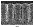
- Figure 1 provides a scanning electron microscope (SEM) image of AlN film deposited using tris(dimethylamino)aluminum and nitrogen plasma at 300 °C, thus demonstrating almost 100% conformality.
- Example 3 PEALD aluminum nitride films using tris(dimethylamino)aluminum (TDMAA) in CN-1 shower head type reactor and nitrogen/argon plasma
- the silicon wafer was loaded into the CN-1 reactor equipped with showerhead design with 13.56 MHz direct plasma and heated to from 100 to 350 °C with chamber pressure of 1 torr (0.13 kPa).
- TDMAA as aluminum precursor was delivered using bubbling method with Ar carrier gas flow rate of 50 sccm into the reactor.
- the PEALD cycle was comprised of the process steps provided in Table 2 and using the following process parameters repeated for 100 cycles:
- Example 4 PEALD aluminum nitride films using tris(dimethylamino)aluminum (TDMAA) in CN-1 shower head type reactor and nitrogen/helium plasma
- the silicon wafer was loaded into the CN-1 reactor equipped with showerhead design with 13.56 MHz direct plasma and heated to from 100 to 350 °C with chamber pressure of 1 torr (0.13 kPa).
- TDMAA as aluminum precursor was delivered using bubbling method with Ar carrier gas flow rate of 50 sccm into the reactor.
- the PEALD cycle was comprised of the process steps provided in Table 2 and using the following process parameters repeated for 100 cycles:
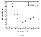
- Figure 3 shows AIN films deposited using tris(dimethylamino)aluminum and 100% nitrogen plasma (Example 2), tris(dimethylamino)aluminum (Example 3) and 50% nitrogen/50% argon plasma, and 50% nitrogen/50% helium plasma (Example 4), demonstrating ALD window from 200 to 350 °C.
- Figure 4 shows reflective index (RI) of AIN film deposited using tris(dimethylamino)aluminum and 100% nitrogen plasma, tris(dimethylamino)aluminum and 50% nitrogen/50% argon plasma, and 50% nitrogen/50% helium plasma, demonstrating high quality AIN films with RI greater than 2.0 can be achieved.
- Tables 3 and 4 summarize AIN film properties.
- Table 3 AIN Film Properties Using the CN-1 with shower head type reactor Temp RF at% at% at% at% at% at% Run # °C Watts N Al H O C N/Al TDMAA+NH 3 thermal or PEALD 3783 300 0 37.23 34.31 25.33 1.03 2.06 1.08 3792 300 200 35.83 35.84 27.03 1.22 0.05 1.00 3796 350 0 34.39 35.65 27.19 0.78 1.95 0.96 TDMAA+N 2 only PEALD 3857 300 200 41.74 41.84 13.89 0.73 1.71 1.00 3908 350 200 42.24 44.6 11.34 0.54 1.25 0.95 TDMAA+N 2 /Ar PEALD 3816 300 200 40.98 40.56 16.14 0.62 1.62 1.01 3827 350 200 41.69 43.17 13.28 0.46 1.31 0.97 TMA+N 2 only PEALD 3916 300 200 40.15 44.35 12.36 1.3 1.79 0.91 3924 350 200 41.31 45.85 9.69 1.85
- Example 5 PEALD boron nitride films using tris(dimethylamino)borane (TDMAB) in CN-1 shower head type reactor and nitrogen plasma
- the silicon wafer was loaded into the CN-1 reactor equipped with showerhead design with 13.56 MHz direct plasma and heated to from 200 to 400 °C with chamber pressure of 2 torr (0.27 kPa).
- TDMAB as boron precursor was delivered using vapor draw method into the reactor.
- the PEALD cycle was comprised of the process steps provided in Table 2 and using the following process parameters repeated for 200 cycles:
- Figure 5 shows thickness of BN films deposited using tris(dimethylamino)borane (TDMAB) and 100% nitrogen plasma vs TDMAB pulse time, demonstrating TDMAB reach self-limiting at 0.5 second.
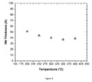
- Figure 6 shows BN films deposited using tris(dimethylamino)borane and 100% nitrogen plasma, demonstrating ALD window from 200 to 400 °C.
- the thickness of BN films vs number of cycles were conducted, the growth rate per cycle was determined from a graph of thickness vs number of cycles as 0.1 ⁇ /cycle.
- Example 6 PEALD aluminum doped titanium nitride film using tris(dimethylamino)aluminum (TDMAA) and tetrakis(dimethylamino)titanium (TDMAT), and nitrogen plasma
- the silicon wafer was loaded into the CN-1 reactor equipped with showerhead design with 13.56 MHz direct plasma and heated to 300 °C with chamber pressure of 2 torr (0.27 kPa). Plasma power was at at 125W. Tris(dimethylamino)aluminum (TDMAA) as aluminum precursor and tetrakis(dimethylamino)titanium (TDMAT) as titanium precursor were delivered using bubbling methods with Ar carrier gas flow rate of 50 sccm into the reactor. Nitrogen plasma was used for plasma. In order to tune aluminum content as well as properties of aluminum doped titanium nitride, the following experiments were performed:
- Figure 7 shows the resistivity of as-deposited aluminum doped titanium nitride films, demonstrating that the resistivity can be tuned via changing ALD conditions.
- Example 7 PEALD boron doped titanium nitride film using tris(dimethylamino)borane (TDMAB) and tetrakis(dimethylamino)titanium (TDMAT), and nitrogen plasma
- the silicon wafer was loaded into the CN-1 reactor equipped with showerhead design with 13.56 MHz direct plasma and heated to 300 °C with chamber pressure of 2 torr (0.27 kPa). Plasma power was at 125W.
- Tris(dimethylamino)borane (TDMAB) as boron precursor was delivered using vapor draw and tetrakis(dimethylamino)titanium (TDMAT) as titanium precursor was delivered using bubbling method with Ar carrier gas flow rate of 50 sccm into the reactor. Nitrogen plasma was used for plasma.
- TDMAB Tris(dimethylamino)borane
- TDMAT tetrakis(dimethylamino)titanium
- Nitrogen plasma was used for plasma.
- Figure 8 shows the resistivity of as-deposited boron doped titanium nitride films, demonstrating that the resistivity can be tuned via changing ALD conditions.
Landscapes
- Chemical & Material Sciences (AREA)
- Engineering & Computer Science (AREA)
- General Chemical & Material Sciences (AREA)
- Chemical Kinetics & Catalysis (AREA)
- Materials Engineering (AREA)
- Mechanical Engineering (AREA)
- Metallurgy (AREA)
- Organic Chemistry (AREA)
- Inorganic Chemistry (AREA)
- Physics & Mathematics (AREA)
- Plasma & Fusion (AREA)
- Electromagnetism (AREA)
- Health & Medical Sciences (AREA)
- Toxicology (AREA)
- Chemical Vapour Deposition (AREA)
- Formation Of Insulating Films (AREA)
Abstract
Description
- Described herein is a method for depositing a stoichiometric or non-stoichiometric metal or a metalloid nitride film of a metal from Group 13 of the Periodic Table using one or more Group 13 metal or metalloid precursors. More specifically, described herein are plasma-based methods for depositing films including, but not limited to, plasma enhanced atomic layer deposition ("PEALD"), and PEALD-like plasma enhanced cyclic chemical vapor deposition ("PECCVD") methods that are typically used for depositing Group 13 metal or metalloid films such as aluminum, gallium, indium, thallium, boron, or combinations thereof that can be used, for example, in the fabrication of integrated circuit devices. Because of their combination of unique properties, Group 13 metal or metalloid containing films, such as, without limitation, aluminum nitride (AIN) or boron nitride (BN) films, can be used for a variety of electronic applications.
- The prior art provides different methods for preparing and using Group 13 metal or metalloid films such as AIN films. For example, the reference "The influence of N2/H2 and ammonia N source materials on optical and structural properties of AIN films grown by plasma enhanced atomic layer deposition," Alevli, M., et al., J. Cryst. Growth, Vol. 335(1): 51-57 (2011), discloses the influence of N2/H2 and ammonia as N source materials on the properties of AIN films grown by plasma enhanced atomic layer deposition using trimethylaluminum as the metal. The AIN growth rate per cycle was decreased from 0.84 to 0.54 Å/cycle (1Å (Angstrom) = 10-9 m) when the N source was changed from NH3 to N2/H2. Growth rate of AIN remained constant within 100-200 °C for both N precursors, confirming the self-limiting growth mode in the ALD window.
- The reference "Optical properties of AIN thin films grown by plasma enhanced atomic layer deposition," Alevli, M., et al., J. Vac. Sci. Technol., A, Vol 30(2): 021506/021501-021506/021506 discloses crystalline aluminum nitride (AIN) films that were prepared by plasma enhanced atomic layer deposition within the temperature range of 100 and 500 °C. The reference shows a relationship between growth temperature and optical properties and the refractive indexes of the AIN films were larger than 1.9 within the 300-1000 nm wavelength range.
- The reference, "PEALD AIN: Controlling growth and film crystallinity," Banerjee, S. et al., Physica Status Solidi (C) Current Topics in Solid State Physics, discloses the growth kinetics and material properties of aluminum nitride (AIN) films deposited on Si(111), with plasma enhanced atomic layer deposition (PEALD). Trimethyl aluminum (TMA) and NH3-plasma were used as the precursors.
- The reference, "Atomic layer deposition of AlN for thin membranes using trimethylaluminum and H2/N2 plasma," Goerke, S., et al., Applied Surface Science Vol. 338(0): 35-41 (2015), describes a method for depositing aluminum nitride (AIN) thin films with thicknesses from 20 to 100 nm on silicon, amorphous silica, silicon nitride, and vitreous carbon by plasma enhanced atomic layer deposition (PEALD) using trimethylaluminum (TMA) and a H2/N2 plasma mixture.
- The reference, "Atomic Layer Deposition of AIN with Tris(Dimethylamido)aluminum and NH3," Liu, G., et al., ECS Transactions 41(2): 219-225 (2011) discloses atomic layer deposition of aluminum nitride on Si wafers using tris(dimethylamido)aluminum and ammonia has been investigated in the temperature range from 180 to 400 °C.
- The reference, "Structural and optical characterization of low-temperature ALD crystalline AIN," Motamedi, P. et al., J. Cryst. Growth 421: 45-52 (2015) describes a plasma enhanced atomic layer deposition (PEALD) process has been used to deposit crystalline AIN thin films at 250 °C using nitrogen 5% hydrogen plasma and trimethylaluminum precursors. Films grown on single crystal silicon and sapphire substrates are crystalline with strong (100) preferred orientation.
- The reference, "Self-limiting low-temperature growth of crystalline AIN thin films by plasma-enhanced atomic layer deposition," Ozgit, C., et al., Thin Solid Films 520(7): 2750-2755 (2012) described PEALD depositions of aluminum-containing films on various substrates using AlMe3 and NH3.
- The reference, "Influence of plasma chemistry on impurity incorporation in AIN prepared by plasma enhanced atomic layer deposition," Perros, A. P., et al., Journal of Physics D: Applied Physics 46(50): 505502 described PEALD depositions of AIN films using NH3, N2 /H2, and N2 plasmas and TMA as the precursor. Different atomistic growth mechanisms are found to exist between the plasma chemistries. The N2 plasma is shown as not suitable for the low-temperature deposition of AIN. Films deposited by NH3 - and N2 /H2 -based processes are nitrogen rich and heavily hydrogenated. Carbon impurities exist at higher concentrations for the N2 /H2 -processes. The discovery of nitrile groups in the films indicates that carbon impurities can be partially attributed to an undesirable reaction occurring during the plasma step between nitrogen species and CH groups.
- The reference, "Structural properties of AlN films deposited by plasma-enhanced atomic layer deposition at different growth temperatures," Alevli, M., et al., Phys. Status Solidi A 209(2): 266-271 (2012) describes the preparation of crystalline aluminum nitride (AIN) films by PEALD within the temp. range from 100° to 500 °C.
- The reference, "Deposition and characterization of BN/Si(001) using tris(dimethylamino)borane," Dumont, H. et al., Mater. Res. Bull. Vol. 37(9), pp. 1565-1572 (2002), describes using a chemical vapor deposition process to deposit BN thin films on Si(001) at temperatures ranging from 750 °C and 1000 °C using (tris(dimethylamino)borane as the precursor.
-
US Pat. No. 7,141,500 discloses a method of forming an aluminum containing film such as aluminum oxide, aluminum nitride, or aluminum oxynitride on a substrate comprising: providing a precursor having the structure Al(NR1R2)(NR3R4)(NR5R6) where each of R1, R2, R3, R4, R5, and R6 is independently selected from the group consisting of hydrogen and an alkyl group including at least 2 carbon atoms. Each of the R1 - R6 groups can be the same or different and can by straight or branched chain alkyls. An exemplary precursor that is useful in forming Al containing films is trisdiethylamino aluminum. -
US Pub. No. 2005/0208718 discloses a method for forming a capacitor using an atomic layer deposition (ALD) process include providing a reactant including an Al precursor onto a substrate to chemisorb a portion of the reactant to a surface of the substrate. An NH3 plasma is provided onto the substrate to form a dielectric layer including Al nitride on the substrate including the lower electrode. - Accordingly, there is a need in the art to provide a low temperature (e.g., processing temperature of 400 °C or below) method for depositing a conformal, high quality, aluminum nitride film wherein the film has one or more of the following characteristics: a density of 2.4 grams per cubic centimeter (g/cc) or greater, a low wet etch rate (as measured in dilute hydrofluoric acid (HF)), hydrogen content less than 20 at.%, reflective index greater than 2.00 and combinations thereof compared to other aluminum nitride films using other deposition methods.
- Described herein are methods for forming stoichiometric or non-stoichiometric Group 13 metal or metalloid containing films such as aluminum nitride, gallium nitride, indium nitride, thallium nitride, boron nitride, or combinations thereof onto at least a portion of a substrate.
- In one aspect, there is provided a method of forming Group 13 nitride films, such as aluminum nitride, boron nitride, gallium nitride, indium nitride, thallium nitride or combinations thereof, or a Group 13 element doped metal nitride film, the method comprising the steps of:
- a. providing a substrate in a reactor;
- b. introducing into the reactor at least one Group 13 metal or metalloid precursor selected from a borane organoamine complex or a precursor represented by the following Formula I:
MRn(NR1R2)3-n I
wherein M is selected from the group consisting of boron (B), aluminum (Al), gallium (Ga), indium (In), thallium (Th), and combinations thereof; R is selected from a linear or branched C1 to C10 alkyl group, a linear or branched C2 to C10 alkenyl group, a linear or branched C2 to C10 alkynyl group, a C1 to C6 dialkylamino group, an electron withdrawing group, and a C6 to C10 aryl group; R1 is selected from hydrogen, a linear or branched C1 to C10 alkyl group, a linear or branched C3 to C10 alkenyl group, a linear or branched C3 to C10 alkynyl group, a C1 to C6 dialkylamino group, an electron withdrawing group, and a C6 to C10 aryl group; R2 is selected from a linear or branched C1 to C10 alkyl group, a linear or branched C3 to C6 alkenyl group, a linear or branched C3 to C6 alkynyl group, a C1 to C6 dialkylamino group, a C6 to C10 aryl group, a linear or branched C1 to C6 fluorinated alkyl group, an electron withdrawing group, and a C4 to C10 aryl group; optionally wherein R1 and R2 are linked together to form a ring selected from a substituted or unsubstituted aromatic ring or a substituted or unsubstituted aliphatic ring; and n=0, 1, 2 or 3, wherein the at least one Group 13 metal or metalloid precursor reacts on at least a portion of the surface of the substrate to provide a chemisorbed layer; - c. purging the reactor with a purge gas;
- d. introducing a plasma comprising nitrogen into the reactor to react with at least a portion of the chemisorbed layer and provide at least one reactive site wherein the plasma is generated at a power density ranging from about 0.01 to about 1.5 W/cm2; and
- e. optionally purging the reactor with an inert gas; and wherein steps b through e are repeated until a desired thickness of the film is obtained. In certain embodiments, R1 and R2 are the same. In other embodiments, R1 and R2 are different. In the foregoing or other embodiments, R1 and R2 can be linked together to form a ring. In yet further embodiments, R1 and R2 are not linked together to form a ring. In a still further embodiment, the plasma comprises a non-hydrogen containing nitrogen plasma selected from the group consisting of nitrogen plasma, nitrogen/helium plasma, nitrogen/argon plasma, nitrogen/neon plasma.
- In another aspect, there is provided a method of forming an aluminum nitride film via plasma enhanced atomic layer deposition process or PEALD-like process, the method comprising the steps of:
- a. providing a substrate in a reactor;
- b. introducing into the reactor at least one aluminum precursor selected from the group consisting of trimethylaluminum, triethylaluminum, tris(dimethylamino)aluminum, and tris(ethylmethylamino)aluminum wherein the at least one aluminum precursor reacts on at least a portion of the surface of the substrate to provide a chemisorbed layer;
- c. purging the reactor with a purge gas comprising at least one selected from nitrogen, a noble gas, and combinations thereof;
- d. introducing a plasma comprising non-hydrogen containing nitrogen plasma into the reactor to react with at least a portion of the chemisorbed layer and provide at least one reactive site wherein the plasma is generated at a power density ranging from 0.01 to 1.5 W/cm2; and
- e. optionally purging the reactor with an inert gas; and wherein steps b through e are repeated until a desired thickness of the aluminum nitride film is obtained
- Aspects of the present invention include the following aspects, numbered #1 to #34:
- #1. A method of forming a Group 13 metal or metalloid nitride film selected from the group consisting of aluminum nitride, boron nitride, gallium nitride, indium nitride, thallium nitride and combinations thereof via a plasma enhanced atomic layer deposition process (PEALD) or a PEALD-like process, the method comprising the steps of:
- a. providing a substrate in a reactor;
- b. introducing into the reactor an at least one Group 13 metal or metalloid precursor represented by the following Formula I:
MRn(NR1R2)3-n I
- wherein M is selected from the group consisting of boron (B), aluminum (Al), gallium (Ga), indium (In), thallium (Th), and combinations thereof; R is selected from a linear or branched C1 to C10 alkyl group, a linear or branched C2 to C10 alkenyl group, a linear or branched C2 to C10 alkynyl group, a C1 to C6 dialkylamino group, an electron withdrawing group, and a C6 to C10 aryl group; R1 is selected from hydrogen, a linear or branched C1 to C10 alkyl group, a linear or branched C3 to C10 alkenyl group, a linear or branched C3 to C10 alkynyl group, a C1 to C6 dialkylamino group, an electron withdrawing group, and a C6 to C10 aryl group; R2 is selected from a linear or branched C1 to C10 alkyl group, a linear or branched C3 to C6 alkenyl group, a linear or branched C3 to C6 alkynyl group, a C1 to C6 dialkylamino group, a C6 to C10 aryl group, a linear or branched C1 to C6 fluorinated alkyl group, an electron withdrawing group, and a C4 to C10 aryl group; optionally wherein R1 and R2 are linked together to form a ring selected from a substituted or unsubstituted aromatic ring or a substituted or unsubstituted aliphatic ring;
- wherein n=0, 1, 2 or 3, wherein the at least one precursor reacts on at least a portion of the surface of the substrate to provide a chemisorbed layer;
- c. purging the reactor with a purge gas;
- d. introducing a plasma comprising non-hydrogen containing nitrogen plasma into the reactor to react with at least a portion of the chemisorbed layer and provide at least one reactive site wherein the plasma is generated at a power density ranging from about 0.01 to about 1.5 W/cm2; and
- e. optionally purge the reactor with an inert gas, wherein the steps b through e are repeated until a desired thickness of the film is obtained.
- #2. The method of
Aspect # 1 wherein the at least one Group 13 metal or metalloid precursor is selected from the group consisting of trimethylaluminum, triethylaluminum, tris(dimethylamino)aluminum, tris(ethylmethylamino)aluminum, trimethylborane, triethylborane, tris(dimethylamino)borane, tris(ethylmethylamino)borane, tris(diethylamino)borane, and a borane organoamine complex. - #3. The method of
Aspect # 2 wherein the at least one Group 13 metal or metalloid precursor is the borane organoamine complex. - #4. The method of Aspect #3 wherein the borane organoamine complex is selected from the group consisting of borane trimethylamine complex, borane triethylamine complex, dimethylamine borane, borane pyridine complex, borane morpholine complex, borane tert-butylamine complex, borane 4-methylmorpholine complex, borane N,N-diisopropylethylamine complex, borane ethylenediamine complex, and 2-Methylpyridine borane complex.
- #5. The method of
Aspect # 1 wherein the method is accomplished via plasma enhanced atomic layer deposition process. - #6. The method of
Aspect # 1 wherein the method is accomplished via the PEALD-like process. - #7. The method of
Aspect # 1 wherein the plasma comprising nitrogen comprises a gas is selected from the group consisting of nitrogen plasma, nitrogen/helium plasma, nitrogen/argon. - #8. The method of
Aspect # 1 wherein the purge gas is a noble gas. - #9. The method of
Aspect # 1 wherein the introducing a plasma step comprises applying energy to create the plasma wherein the energy is provided by at least one of the sources selected from the group consisting of thermal, plasma, pulsed plasma, helicon plasma, high density plasma, inductively coupled plasma, X-ray, e-beam, photon, remote plasma methods, and combinations thereof. - #10. The method of
Aspect # 1 wherein R1 and R2 are the same. - #11. The method of
Aspect # 1 wherein R1 and R2 are different. - #12. The method of
Aspect # 1 wherein R1 and R2 are linked together to form a ring. - #13. The method of
Aspect # 1 further comprising the step of, prior to step d, introducing a plasma comprising hydrogen. - #14. The method of
Aspect # 1 further comprising the step of treating the film once the desired thickness is achieved, wherein the treating is accomplished by exposure to an energy source selected from the group consisting of hydrogen plasma, helium plasma, argon plasma, UV radiation, IR radiation, and combination thereof. - #15. A method of forming an aluminum nitride film, the method comprising the steps of:
- a. providing a substrate in a reactor;
- b. introducing into the reactor an at least one aluminum precursor selected from the group consisting of trimethylaluminum, triethylaluminum, tris(dimethylamino)aluminum, and tris(ethylmethylamino)aluminum wherein the at least one aluminum precursor reacts on at least a portion of the surface of the substrate to provide a chemisorbed layer;
- c. purging the reactor with a purge gas; and
- d. introducing a plasma comprising non-hydrogen containing nitrogen plasma into the reactor to react with at least a portion of the chemisorbed layer and provide at least one reactive site wherein the plasma is generated at a power density ranging from about 0.01 to about 1.5 W/cm2; and
- e. optionally purge the reactor with an inert gas, wherein the steps b through e are repeated until a desired thickness of the aluminum nitride film is obtained.
- #16. The method of Aspect #15 wherein the method is accomplished via plasma enhanced atomic layer deposition process.
- #17. The method of Aspect #15 wherein the method is accomplished via the PEALD-like process.
- #18. The method of Aspect #15 wherein the non-hydrogen containing nitrogen plasma comprises N2 plasma.
- #19. The method of Aspect #15 wherein the purge gas is a noble gas.
- #20. The method of Aspect #15 wherein the introducing a plasma step comprises applying energy to create the plasma wherein the energy is provided by at least one of the sources selected from the group consisting of thermal, plasma, pulsed plasma, helicon plasma, high density plasma, inductively coupled plasma, X-ray, e-beam, photon, remote plasma methods, and combinations thereof.
- #21. A method of forming a boron nitride film, the method comprising the steps of:
- a. providing a substrate in a reactor;
- b. introducing into the reactor an at least one boron precursor selected from the group consisting of trimethylboron, triethylboron, tris(dimethylamino)borane, and tris(ethylmethylamino)borane, tris(diethylamino)borane wherein the at least one boron precursor reacts on at least a portion of the surface of the substrate to provide a chemisorbed layer;
- c. purging the reactor with a purge gas; and
- d. introducing a plasma comprising non-hydrogen containing nitrogen plasma into the reactor to react with at least a portion of the chemisorbed layer and provide at least one reactive site wherein the plasma is generated at a power density ranging from about 0.01 to about 1.5 W/cm2; and
- e. optionally purge the reactor with an inert gas, wherein the steps b through e are repeated until a desired thickness of the boron nitride film is obtained.
- #22. The method of
Aspect # 20 wherein the method is accomplished via plasma enhanced atomic layer deposition process. - #23. The method of Aspect #21 wherein the method is accomplished via the PEALD-like process.
- #24. The method of Aspect #21 wherein the non-hydrogen containing nitrogen plasma comprises N2 plasma.
- #25. The method of Aspect #21 wherein the purge gas is a noble gas.
- #26. The method of Aspect #21 wherein the introducing a plasma step comprises applying energy to create the plasma wherein the energy is provided by at least one of the sources selected from the group consisting of thermal, plasma, pulsed plasma, helicon plasma, high density plasma, inductively coupled plasma, X-ray, e-beam, photon, remote plasma methods, and combinations thereof.
- #27. A method of forming a Group 13 element doped metal nitride such as aluminum doped titanium nitride, boron doped titanium nitride, aluminum doped tantalum nitride, boron doped tantalum nitride, aluminum doped tungsten nitride, boron doped tungsten nitride, aluminum doped vanadium nitride, boron doped vanadium nitride film via plasma enhanced atomic layer deposition process or PEALD-like process, the method comprising the steps of:
- a. providing a substrate in a reactor;
- b. introducing into the reactor at least one aluminum precursor is selected from the group consisting of trimethylaluminum, triethylaluminum, tris(dimethylamino)aluminum, tris(ethylmethylamino)aluminum, trimethylborane, triethylborane, tris(dimethylamino)borane, tris(ethylmethylamino)borane, tris(diethylamino)borane, and borane organoamine complex wherein the at least one aluminum or boron precursor reacts on at least a portion of the surface of the substrate to provide a chemisorbed layer;
- c. purging the reactor with a purge gas comprising at least one selected from nitrogen, a noble gas, and combinations thereof;
- d. introducing a plasma comprising non-hydrogen containing nitrogen plasma into the reactor to react with at least a portion of the chemisorbed layer and provide at least one reactive site wherein the plasma is generated at a power density ranging from about 0.01 to about 1.5 W/cm2;
- e. purging the reactor with a purge gas comprising at least one selected from nitrogen, a noble gas, and combinations thereof;
- f. introducing into the reactor at least one metal precursor is selected from the group consisting zirconium chloride (ZrCl4), tetrakis(dimethylamino)zirconium (TDMAZ), tetrakis(diethylamino)zirconium (TDEAZ), tetrakis(ethylmethylamino)zirconium (TEMAZ), tetrakis(dimethylamino)hafnium (TDMAH), tetrakis(diethylamino)hafnium (TDEAH), and tetrakis(ethylmethylamino)hafnium (TEMAH), titanium chloride (TiCl4), tetrakis(dimethylamino)titanium (TDMAT), tetrakis(diethylamino)titanium (TDEAT), tetrakis(ethylmethylamino)titanium (TEMAT), tantalum chloride (TaCl5), tert-butylimino tri(diethylamino)tantalum (TBTDET), tert-butylimino tri(dimethylamino)tantalum (TBTDMT), tert-butylimino tri(ethylmethylamino)tantalum (TBTEMT), ethylimino tri(diethylamino)tantalum (EITDET), ethylimino tri(dimethylamino)tantalum (EITDMT), ethylimino tri(ethylmethylamino)tantalum (EITEMT), tert-amylimino tri(dimethylamino)tantalum (TAIMAT), tert-amylimino tri(diethylamino)tantalum, pentakis(dimethylamino)tantalum, tert-amylimino tri(ethylmethylamino)tantalum, tungsten hexachloride, tungsten pentachloride, bis(tert-butylimino)bis(dimethylamino)tungsten (BTBMW), bis(tert-butylimino)bis(diethylamino)tungsten, bis(tert-butylimino)bis(ethylmethylamino)tungsten, and combinations thereof wherein the at least one metal precursor reacts on at least a portion of the surface of the substrate to provide a chemisorbed layer;
- g. purging the reactor with a purge gas comprising at least one selected from nitrogen, a noble gas, and combinations thereof;
- h. introducing a plasma comprising non-hydrogen containing nitrogen plasma into the reactor to react with at least a portion of the chemisorbed layer and provide at least one reactive site wherein the plasma is generated at a power density ranging from about 0.01 to about 1.5 W/cm2; and
- i. optionally purging the reactor with an inert gas, wherein the steps b through i are repeated until a desired thickness of the aluminum or boron doped metal nitride film is obtained.
- #28. The method of Aspect #27 wherein the method is accomplished via plasma enhanced atomic layer deposition process.
- #29. The method of Aspect #27 wherein the method is accomplished via the PEALD-like process.
- #30. The method of Aspect #27 wherein the non-hydrogen containing nitrogen plasma comprises N2 plasma.
- #31. The method of Aspect #27 wherein the purge gas is a noble gas.
- #32. The method of Aspect #27 wherein the introducing a plasma step comprises applying energy to create the plasma wherein the energy is provided by at least one of the sources selected from the group consisting of thermal, plasma, pulsed plasma, helicon plasma, high density plasma, inductively coupled plasma, X-ray, e-beam, photon, remote plasma methods, and combinations thereof.
- #33. The method of Aspect #27 wherein steps b to e are repeated to reach a desired a thickness of Group 13 element nitride before step e is performed.
- #34. The method of Aspect #27 wherein steps f to i are repeated more cycles than steps b to e to provide Group 13 element doped metal nitride with Group 13 element content less than 15 at.% by XPS.
-
-
Figure 1 provides a scanning electron microscope (SEM) image of an AIN film deposited using tris(dimethylamino)aluminum and nitrogen plasma, demonstrating almost 100% conformality; -
Figure 2 provides thickness of AIN film deposited using tris(dimethylamino)aluminum and nitrogen plasma vs number of cycles, demonstrating good linearity between film thickness and number of cycles; -
Figure 3 shows thickness of AIN films deposited using tris(dimethylamino)aluminum and 100% nitrogen plasma, tris(dimethylamino)aluminum and 50% nitrogen/50% argon plasma, and tris(dimethylamino)aluminum and 50% nitrogen/50% helium plasma, demonstrating ALD window from 200 to 350 °C.Figure 4 shows the reflective index (RI) of AIN films deposited using tris(dimethylamino)aluminum and 100% nitrogen plasma, tris(dimethylamino)aluminum and 50% nitrogen/50% argon plasma, tri(dimethylamino)aluminum and 50% nitrogen/50% helium plasma, demonstrating high quality AIN films with RI greater than 2.0 can be achieved. Table 3, 4 and 5 summarize ALN film properties; -
Figure 5 shows thickness of BN films deposited using tris(dimethylamino)borane (TDMAB) and 100% nitrogen plasma vs TDMAB pulse time, demonstrating TDMAB reach self-limiting at 0.5 second; -
Figure 6 shows the thickness of BN films deposited using tris(dimethylamino)borane and 100% nitrogen plasma, demonstrating ALD window from 200 to 400 °C; -
Figure 7 shows the resistivity of as-deposited aluminum doped titanium nitride films, demonstrating that the resistivity of aluminum titanium nitride can be tuned via changing ALD conditions; and -
Figure 8 shows the resistivity of as-deposited boron doped titanium nitride, demonstrating that the resistivity of boron titanium nitride can be tuned via changing ALD conditions. - The deposition of conformal Group 13 metal or metalloid nitride films such as, without limitation, aluminum or boron nitride films, at low temperature, e.g., temperatures of 400 °C or less, which meet one or more criteria to be considered a high quality film, has been a long-standing industry challenge. An aluminum nitride film is considered a "high quality" film if it has one or more of the following characteristics: a density of 2.4 grams per cubic centimeter (g/cc) or greater as measured by X-ray-reflectometry (XRR), a low wet etch rate (as measured in dilute hydrofluoric acid (HF)), a hydrogen content of 20 atomic (at.)% or less as measured by Secondary Ion Mass Spectrometry (SIMS), a reflective index greater than 2.00 and combinations thereof.
- Described herein are methods for forming stoichiometric or non-stoichiometric Group 13 nitride films such as aluminum nitride, boron nitride, gallium nitride, indium nitride, thallium nitride and combinations thereof or Group 13 element doped metal nitride films onto at least a portion of a substrate. The Group 13 nitride films such as aluminum nitride, boron nitride, gallium nitride, and indium nitride films or Group 13 element doped metal nitride films described herein are deposited using at least one Group 13 precursor selected from a borane organoamine complex or a precursor represented by the following Formula I:
MRn(NR1R2)3-n I
wherein M is selected from the group consisting of boron (B), aluminum (Al), gallium (Ga), indium (In), and thallium (Th); R is selected from a linear or branched C1 to C10 alkyl group, a linear or branched C2 to C10 alkenyl group, a linear or branched C2 to C10 alkynyl group, a C1 to C6 dialkylamino group, an electron withdrawing group, and a C6 to C10 aryl group; R1 is selected from hydrogen, a linear or branched C1 to C10 alkyl group, a linear or branched C3 to C10 alkenyl group, a linear or branched C3 to C10 alkynyl group, a C1 to C6 dialkylamino group, an electron withdrawing group, and a C6 to C10 aryl group; R2 is selected from a linear or branched C1 to C10 alkyl group, a linear or branched C3 to C6 alkenyl group, a linear or branched C3 to C6 alkynyl group, a C1 to C6 dialkylamino group, a C6 to C10 aryl group, a linear or branched C1 to C6 fluorinated alkyl group, an electron withdrawing group, and a C4 to C10 aryl group; optionally wherein R1 and R2 are linked together to form a ring selected from a substituted or unsubstituted aromatic ring or a substituted or unsubstituted aliphatic ring; and n= 0, 1, 2 or 3. In certain embodiments, R, R1, and R2 are each independently selected from methyl and ethyl. In certain embodiments of Formula I, R, R1, and R2 are methyl. - In the formulae and throughout the description, the term "alkyl" denotes a linear or branched functional group having from 1 to 10 or 1 to 6 carbon atoms. Exemplary alkyl groups include, but are not limited to, methyl (Me), ethyl (Et), propyl (Prn), isopropyl (Pri), butyl (Bun), isobutyl (Bui), sec-butyl (Bus), tert-butyl (But), pentyl, isopentyl, tert-pentyl (Amt), hexyl, iso-hexyl, and neo-hexyl.
- In the formulae and throughout the description, the term "cyclic alkyl" denotes a cyclic functional group having from 3 to 10,from 4 to 10 carbon atoms or from 5 to 10 carbon atoms. Exemplary cyclic alkyl groups include, but are not limited to, cyclobutyl, cyclopentyl, cyclohexyl, and cyclooctyl groups.
- In the formulae and throughout the description, the term "aryl" denotes an aromatic cyclic functional group having from 5 to 12 carbon atoms, from 6 to 10, or from 4 to 10 carbon atoms. Exemplary aryl groups include, but are not limited to, phenyl, benzyl, chlorobenzyl, tolyl, and o-xylyl.
- In the formulae and throughout the description, the term "alkenyl group" denotes a group which has one or more carbon-carbon double bonds and has from 2 to 10, from 3 to 10, from 2 to 6 or from 3 to 4 carbon atoms.
- In the formulae and throughout the description, the term "alkynyl group" denotes a group which has one or more carbon-carbon triple bonds and has from 2 to 10, from 3 to 10, from 3 to 6 or from 3 to 4 carbon atoms.
- In the formulae and throughout the description, the term "dialkylamino group" denotes a group which has two alkyl groups attached to a nitrogen atom and has from 1 to 10, from 2 to 6 or from 2 to 4 carbon atoms. Exemplary dialkylamino groups include, but are not limited to dimethylamino, diethylamino, and ethylmethylamino.
- In the formulae and throughout the description, the term "electron withdrawing group" denotes an atom or group thereof that acts to draw electrons away from the M-N bond. Examples of suitable electron withdrawing groups or substituents include, but are not limited to, nitriles (CN). In certain embodiments, an electron withdrawing substituent can be adjacent to or proximal to N in any one of Formula I. Further, non-limiting examples of an electron withdrawing group include F, Cl, Br, I, CN, NO2, RSO, and/or RSO2, wherein R can be a C1 to C10 alkyl group such as, for example, a methyl group.
- Throughout the description, the term "non-hydrogen containing nitrogen plasma" denotes a plasma that does not having any hydrogen atoms. Examples include, but are not limited, nitrogen plasma, a plasma comprising nitrogen and helium, a plasma comprising nitrogen and argon, a plasma comprising nitrogen and neon. The nitrogen content in the plasma can vary from 0.01 to 100%. Exemplary nitrogen contents include, but are not limited to, 5% nitrogen and 95% helium, 5% nitrogen and 95% argon, 10% nitrogen and 90% helium, 10% nitrogen and 90% argon, 15% nitrogen and 85% helium, 15% nitrogen and 85% argon, 20% nitrogen and 80% helium, 20% nitrogen and 80% argon, 25% nitrogen and 75% helium, 25% nitrogen and 75% argon, 30% nitrogen and 70% helium, 30% nitrogen and 70% argon, 40% nitrogen and 60% helium, 40% nitrogen and 60% argon, 50% nitrogen and 50% helium, 50% nitrogen and 50% argon, 60% nitrogen and 40% argon, 60% nitrogen and 40% helium, 70% nitrogen and 30% argon, 70% nitrogen and 30% helium, 80% nitrogen and 20% argon, 80% nitrogen and 20% helium, 90% nitrogen and 10% argon, 90% nitrogen and 10% helium, 95% nitrogen and 5% argon, 95% nitrogen and 5% helium, 100% nitrogen.
- Throughout the description, the term "conformal" as used herein is defined as a percentage of two thicknesses of the deposited aluminum nitride, boron nitride, gallium nitride, Group 13 element doped metal nitride film in a structured or featured substrate having either vias or trenches or both, with bottom step coverage being the ratio (in %): thickness at the bottom of the feature is divided by thickness at the top of the feature, and middle step coverage being the ratio (in %): thickness on a sidewall of the feature is divided by thickness at the top of the feature. Films deposited using the method described herein exhibit a step coverage of about 60% or greater, about 70% or greater, about 80% or greater, or about 90% or greater which indicates that the films are conformal.
- In certain embodiments, one or more of the alkyl group, alkenyl group, alkynyl group, alkoxy group, dialkylamino group, aryl group, and/or electron withdrawing group in Formula I may be substituted or have one or more atoms or group of atoms substituted in place of a hydrogen atom. Exemplary substituents include, but are not limited to, oxygen, sulfur, halogen atoms (e.g., F, Cl, I, or Br), nitrogen, and phosphorous. For example, the term "fluorinated alkyl group" denotes a group wherein the alkyl group has one or more of its atoms such as a hydrogen atom, substituted with a fluorine atom.
- Exemplary Group 13 metal or metalloid precursors include, but are not limited to, trimethylaluminum, triethylaluminum, tris(dimethylamino)aluminum, tris(ethylmethylamino)aluminum, trimethylborane, triethylborane, tris(dimethylamino)borane, tris(ethylmethylamino)borane, and tris(diethylamino)borane. Further exemplary Group 13 metalloid precursors include a "borane organoamine complex". A "borane organoamine complex" denotes a stable and volatile borane complex formed by reacting borane or diborane with an organoamine. Exemplary organoamine borane complexes include, but are not limited to, borane trimethylamine complex, borane triethylamine complex, dimethylamine borane, borane pyridine complex, borane morpholine complex, borane tert-butylamine complex, borane 4-methylmorpholine complex, borane N,N-diisopropylethylamine complex, borane ethylenediamine complex, and 2-Methylpyridine borane complex.
- The process used to form Group 13 metal or metalloid nitride or metal doped metalloid films includes any suitable deposition process. Examples of suitable deposition processes include, but are not limited to, plasma enhanced ALD (PEALD) or PEALD-like process. As used herein, the term "chemical vapor deposition processes" refers to any process wherein a substrate is exposed to one or more volatile precursors, which react and/or decompose on the substrate surface to produce the desired deposition. As used herein, the term "atomic layer deposition process" refers to a self-limiting (e.g., the amount of film material deposited in each reaction cycle is constant), sequential surface chemistry that deposits films of materials onto substrates of varying compositions. Although the precursors, reagents and sources used herein may be sometimes described as "gaseous," it is understood that the precursors can be either liquid or solid which are transported with or without an inert gas into the reactor via direct vaporization, bubbling or sublimation. In some case, the vaporized precursors can pass through a plasma generator. The term "reactor" as used herein, includes without limitation, reaction chamber or deposition chamber such as a single wafer ALD reactor, semi-batch ALD reactor, or batch furnace ALD reactor; b) each reactant including aluminum precursor or boron precursor or metal precursor and reactive gas is exposed to a substrate by moving or rotating the substrate to different sections of the reactor and each section is separated by inert gas curtain, i.e. spatial ALD reactor or roll to roll ALD reactor. The "PEALD-like" process is defined herein as a plasma enhanced cyclic CVD process that provides a high conformal aluminum nitride or boron nitride or metal doped aluminum nitride or metal doped boron nitride film on a substrate as shown by having at least one of the following: percentage of non-uniformity of 5% or less as measured by ellipsometer, a deposition rate of 0.1 Å or greater per cycle, or a combination thereof.
- In certain embodiments, the method disclosed herein avoids pre-reaction of the precursors by using PEALD or PEALD-like methods that separate the precursors prior to and/or during the introduction to the reactor. In this connection, deposition techniques such as PEALD or PEALD-like processes are used to deposit Group 13 metal or metalloid nitride film. In one embodiment, the film is deposited via a PEALD process by exposing the substrate surface alternatively to the one or more the aluminum nitride precursor, nitrogen-containing source, or other precursor or reagent. Film growth proceeds by self-limiting control of surface reaction, the pulse length of each precursor or reagent, and the deposition temperature. However, once the surface of the substrate is saturated, the film growth ceases.
- Depending upon the deposition method, in certain embodiments, the at least one Group 13 metal or metalloid precursors may be introduced into the reactor at a predetermined molar volume such as, for example, from 0.1 to 1000 micromoles. In this embodiment, the at least one aluminum precursor may be introduced into the reactor for a predetermined time period. In certain embodiments, the time period ranges from 0.001 to 500 seconds.
- In certain embodiments, the Group 13 metal or metalloid nitride films comprise aluminum and/or nitrogen or boron and/or nitrogen. In these embodiments, the aluminum or boron nitride films deposited using the methods described herein are formed in the presence of a nitrogen-containing source. A nitrogen-containing source may be introduced into the reactor in the form of at least one nitrogen-containing source and/or may be present incidentally in the other precursors used in the deposition process. Suitable nitrogen-containing source gases may include, for example, a nitrogen/argon plasma. In certain embodiments, the nitrogen-containing source comprises a nitrogen/argon plasma source gas that is introduced into the reactor at a flow rate ranging from 1 to 2000 standard cubic centimeters (sccm) or from 1 to 1000 sccm. The nitrogen-containing source can be introduced for a time that ranges from 0.1 to 100 seconds. In embodiments wherein the film is deposited by an ALD or a cyclic CVD process, the precursor pulse can have a pulse duration that is greater than 0.01 seconds, and the nitrogen-containing source can have a pulse duration that is less than 0.01 seconds, while the water pulse duration can have a pulse duration that is less than 0.01 seconds. In yet another embodiment, the purge duration between the pulses can be as low as 0 seconds or is continuously pulsed without a purge in-between.
- In the method described herein, a nitrogen-containing plasma comprising a nitrogen containing gas such as, without limitation, nitrogen and optionally a noble gas can be generated in situ or remotely. In a preferred embodiment, the noble gas has an atomic mass greater than nitrogen's atomic mass (i.e., 28 amu). The presence of a noble gas with atomic mass greater than nitrogen's atomic mass is believed to create more atomic nitrogen radicals. The nitrogen plasma source gas is introduced into the reactor at a flow rate ranging from 1 to 2000 square cubic centimeters (sccm) or from 1 to 1000 sccm or more. The nitrogen containing plasma can be introduced for a time that ranges from 0.01 to 100 seconds or more. In embodiments, the precursor pulse can have a pulse duration that is greater than 0.01 seconds, and the nitrogen-containing plasma can have a pulse duration that is less than 0.01 seconds, while the water pulse duration can have a pulse duration that is less than 0.01 seconds. In yet another embodiment, the purge duration between the precursor pulse and nitrogen plasmas can be as low as 0 seconds. In yet another embodiment, a hydrogen plasma can be generated in situ or remotely using pure hydrogen (H2) mixed with a noble gas when a hydrogen plasma can be employed. The weight percentage of the noble gas in the plasma containing both nitrogen and noble gas can vary from 1 wt% to 99 wt% whereas the weight percentage of the noble gas in the plasma containing both hydrogen and noble gas can also vary from 1 wt% to 99 wt%.
- As demonstrated in the working examples herein, conventional nitrogen containing plasma disclosed in the prior art such as ammonia plasma and hydrogen/nitrogen plasma could not provide high quality Group 13 metal or metalloid nitride films using existing aluminum or boron precursors such as tris(dimethylamino)aluminum or tris(dimethylamino)borane. Without being bound by a particular theory, it is believed the plasma containing only nitrogen or both nitrogen and a noble gas such as helium or argon can help the formation of Group 13 metal or metalloid films such as an aluminum or boron nitride film as well as provide reactive sites on at least a portion of the chemisorbed surface for aluminum or boron precursors having Formula I in subsequent deposition cycles to anchor onto these reactive sites. This enables the cyclical deposition to occur whereas conventional nitrogen containing plasma such as ammonia plasma and/or hydrogen/nitrogen plasma may poison the surface, thereby resulting in minimum film deposition. Not being bound by any theory, the plasma density which is defined by plasma power over area of electrodes (for example, plasma power of 450W for a 6" wafer ALD reactor, the plasma density is 2.5W/cm2, assuming the area of electrode is same as the wafer) and is preferably lower than 2 W/cm2 in order to reduce potential plasma damage on the substrate as well as any built-in structures on the substrate, yet still produce high quality aluminum nitride film which can be implemented into semi-conductor manufacturing processes. The plasma density of the method described herein ranges from 0.01 to 2 W/cm2, or from 0.01 to 1.5 W/cm2, or from 0.01 to 1 W/cm2. Typical plasma frequency ranges from 10 KHz to 2.4 GHz, preferably 10 kHz to 60 MHz. In some embodiments, dual RF plasma can be employed, one low frequency ranging from 10 kHz to 1 MHz and the other middle frequency selected from group consisting of 13.56 MHz and 27.1 MHz.
- The deposition methods described herein may involve one or more purge gases. The purge gas, which is used to purge away unconsumed reactants and/or reaction byproducts, is an inert gas that does not react with the precursors. Exemplary purge gases include, but are not limited to, argon (Ar), nitrogen (N2), helium (He), neon (Ne), hydrogen (H2), and mixtures thereof. In certain embodiments, the inert gas that is used as a purge gas comprises a noble gas. The term "noble gas" as used herein means those gases found in Group 18 of the Periodic Table and includes, helium (He), neon (Ne), argon (Ar), Xenon (Xe), krypton (Kr), and mixtures thereof. In one particular embodiment, the noble gas used as a purge gas comprises argon. In this or other embodiments, the purge gas comprising Ar is supplied into the reactor at a flow rate ranging from 10 to 2000 sccm for 0.1 to 1000 seconds, thereby purging the unreacted precursor material and any byproduct that may remain in the reactor.
- The respective step of supplying the precursors, the nitrogen-containing source, and/or other precursors, source gases, and/or reagents may be performed by changing the time for supplying them to change the stoichiometric composition of the resulting aluminum nitride film.
- Energy is applied to the at least one of the precursor, nitrogen-containing source, reducing agent, other precursors or combination thereof to induce reaction and to form the aluminum nitride film or coating on the substrate. Such energy can be provided by, but not limited to, thermal, plasma, pulsed plasma, helicon plasma, high density plasma, inductively coupled plasma, X-ray, e-beam, photon, remote plasma methods, and combinations thereof. In certain embodiments, a secondary RF frequency source can be used to modify the plasma characteristics at the substrate surface. In embodiments wherein the deposition involves plasma, the plasma-generated process may comprise a direct plasma-generated process in which plasma is directly generated in the reactor, or alternatively a remote plasma-generated process in which plasma is generated outside of the reactor and supplied into the reactor.
- The Group 13 metal or metalloid precursors may be delivered to the reaction chamber such as a PEALD or PEALD-like reactor either single wafer or batch in a variety of ways such as bubbling, vapor draw, or direct liquid injection (DLI). In one embodiment, a liquid delivery system may be utilized. In an alternative embodiment, a combined liquid delivery and flash vaporization process unit may be employed, such as, for example, the turbo vaporizer manufactured by MSP Corporation of Shoreview, MN, to enable low volatility materials to be volumetrically delivered, which leads to reproducible transport and deposition without thermal decomposition of the precursor. In liquid delivery formulations, the precursors described herein may be delivered in neat liquid form, or alternatively, may be employed in solvent formulations or compositions comprising same. Thus, in certain embodiments the precursor formulations may include solvent component(s) of suitable character as may be desirable and advantageous in a given end use application to form a film on a substrate.
In certain embodiments, gas lines connecting from the precursor canisters to the reaction chamber are heated to one or more temperatures depending upon the process requirements and the container of the aluminum precursor having the Formula I described herein is kept at one or more temperatures for bubbling. In other embodiments, a solution comprising the at least one aluminum nitride precursor having the formula described herein is injected into a vaporizer kept at one or more temperatures for direct liquid injection. - A flow of argon and/or other inert gas may be employed as a carrier gas to help deliver the vapor of the at least one aluminum precursor to the reaction chamber during the precursor pulsing. In certain embodiments, the reaction chamber process pressure is 2 Torr (0.27 kPa) or less. In other embodiments, the reaction chamber process pressure is 10 Torr (1.3 kPa) or less. In other embodiments, the reaction chamber process pressure is 200 Torr (26.7 kPa) or less.
- In a typical PEALD or PEALD-like process, a substrate such as, without limitation, a silicon oxide, carbon doped silicon oxide, flexible substrate, or metal nitride substrate is heated on a heater stage in a reaction chamber that is exposed to the aluminum nitride precursor initially to allow the aluminum to chemically adsorb onto the surface of the substrate. A purge gas such as nitrogen, argon, or other inert gas purges away unabsorbed excess aluminum from the process chamber. After sufficient purging, an nitrogen-containing source may be introduced into reaction chamber to react with the absorbed surface followed by another gas purge to remove reaction by-products from the chamber. The process cycle can be repeated to achieve the desired film thickness. In other embodiments, pumping under vacuum can be used to remove unabsorbed excess aluminum from the process chamber, after sufficient evacuation under pumping, a nitrogen-containing source may be introduced into reaction chamber to react with the absorbed surface followed by another pumping down purge to remove reaction by-products from the chamber.
- In one aspect, there is provided a method of forming a Group 13 nitride film selected from the group consisting of aluminum nitride, boron nitride, gallium nitride, indium nitride, thallium nitride and combinations thereof, the method comprising the steps of:
- a. providing a substrate in a reactor;
- b. introducing into the reactor an at least one Group 13 precursor represented by the following Formula I:
MRn(NR1R2)3-n I
wherein M is selected from the group consisting of boron (B), aluminum (Al), gallium (Ga), indium (In), thallium (Th), and combinations thereof; R is selected from a linear or branched C1 to C10 alkyl group, a linear or branched C2 to C10 alkenyl group, a linear or branched C2 to C10 alkynyl group, a C1 to C6 dialkylamino group, an electron withdrawing group, and a C6 to C10 aryl group; R1 is selected from hydrogen, a linear or branched C1 to C10 alkyl group, a linear or branched C3 to C10 alkenyl group, a linear or branched C3 to C10 alkynyl group, a C1 to C6 dialkylamino group, an electron withdrawing group, and a C6 to C10 aryl group; R2 is selected from a linear or branched C1 to C10 alkyl group, a linear or branched C3 to C6 alkenyl group, a linear or branched C3 to C6 alkynyl group, a C1 to C6 dialkylamino group, a C6 to C10 aryl group, a linear or branched C1 to C6 fluorinated alkyl group, an electron withdrawing group, and a C4 to C10 aryl group; optionally wherein R1 and R2 are linked together to form a ring selected from a substituted or unsubstituted aromatic ring or a substituted or unsubstituted aliphatic ring; and wherein n=0,1, 2 or 3, wherein the at least one aluminum precursor reacts on at least a portion of the surface of the substrate to provide a chemisorbed layer; - c. purging the reactor with a purge gas;
- d. introducing a plasma comprising nitrogen plasma into the reactor to react with at least a portion of the chemisorbed layer and provide at least one reactive site wherein the plasma is generated at a power density ranging from about 0.01 to about 1.5 W/cm2; and
- e. optionally purging the reactor with an inert gas; and wherein steps b through e are repeated until a desired thickness of the Group 13 metal or metalloid nitride film is obtained. In certain embodiments, R1 and R2 are the same. In other embodiments, R1 and R2 are different. In the foregoing or other embodiments, R1 and R2 can be linked together to form a ring. Examples of the ring include but are not limited to pyrrolidino wherein R1 = R2 = linear C2 alkyl, 2,5-dimethyl- pyrrolidino wherein R1 =R2= branched C3 alkyl, piperidino wherein R1 = R2 = linear C3 alkyl, 2,6-dimethylpiperidino wherein R1 = branched C3 alkyl and R2= branched C4 alkyl. In yet further embodiments, R1 and R2 are not linked together to form a ring. Optionally a plasma comprising hydrogen can be inserted before step d to help remove hydrocarbon generated from the reaction between the Group 13 precursor and the surface. In certain embodiments, the plasma comprising nitrogen is selected from the group consisting of nitrogen plasma, nitrogen/helium, nitrogen/argon plasma, nitrogen/neon plasma and mixtures thereof. In alternative embodiments, the plasma comprises a non-hydrogen plasma.
- In another aspect, there is provided a method of forming an aluminum nitride film via plasma enhanced atomic layer deposition process or PEALD-like process, the method comprising the steps of:
- a. providing a substrate in a reactor;
- b. introducing into the reactor at least one aluminum precursor selected from the group consisting of trimethylaluminum, triethylaluminum, tris(dimethylamino)aluminum, and tris(ethylmethylamino)aluminum wherein the at least one aluminum precursor reacts on at least a portion of the surface of the substrate to provide a chemisorbed layer;
- c. purging the reactor with a purge gas comprising at least one selected from nitrogen, a noble gas, and combinations thereof;
- d. introducing a plasma comprising non-hydrogen containing nitrogen plasma into the reactor to react with at least a portion of the chemisorbed layer and provide at least one reactive site wherein the plasma is generated at a power density ranging from 0.01 to 1.5 W/cm2; and
- e. optionally purging the reactor with an inert gas; and wherein steps b through e are repeated until a desired thickness of the aluminum nitride film is obtained.
- In another aspect, there is provided a method of forming a boron nitride film via plasma enhanced atomic layer deposition process or PEALD-like process, the method comprising the steps of:
- a. providing a substrate in a reactor;
- b. introducing into the reactor at least one boron precursor selected from the group consisting of trimethylborane, triethylborane, tris(dimethylamino)borane, tris(ethylmethylamino)borane, tris(diethylamino)borane, and a borane organoamine complex wherein the at least one boron precursor reacts on at least a portion of the surface of the substrate to provide a chemisorbed layer;
- c. purging the reactor with a purge gas comprising at least one selected from nitrogen, a noble gas, and combinations thereof;
- d. introducing a plasma comprising non-hydrogen containing nitrogen plasma into the reactor to react with at least a portion of the chemisorbed layer and provide at least one reactive site wherein the plasma is generated at a power density ranging from 0.01 to 1.5 W/cm2; and
- e. optionally purging the reactor with an inert gas; and wherein steps b through e are repeated until a desired thickness of the boron nitride film is obtained.
- In another aspect, there is provided a method of forming a Group 13 nitride having two different Group 13 elements such as a boron doped aluminum nitride film via plasma enhanced atomic layer deposition process or PEALD-like process, the method comprising the steps of:
- a. providing a substrate in a reactor;
- b. introducing into the reactor at least one aluminum precursor selected from the group consisting of trimethylaluminum, triethylaluminum, tris(dimethylamino)aluminum, and tris(ethylmethylamino)aluminum wherein the at least one aluminum precursor reacts on at least a portion of the surface of the substrate to provide a chemisorbed layer;
- c. purging the reactor with a purge gas comprising at least one selected from nitrogen, a noble gas, and combinations thereof;
- d. introducing a plasma comprising non-hydrogen containing nitrogen plasma into the reactor to react with at least a portion of the chemisorbed layer and provide at least one reactive site wherein the plasma is generated at a power density ranging from about 0.01 to about 1.5 W/cm2;
- e. purging the reactor with a purge gas comprising at least one selected from nitrogen, a noble gas, and combinations thereof;
- f. introducing into the reactor at least one Group 13 precursor other than aluminum such as boron precursor selected from the group consisting of trimethylborane, triethylborane, tris(dimethylamino)borane, tris(ethylmethylamino)borane, tris(diethylamino)borane, and borane organoamine complex wherein the at least one Group 13 precursor reacts on at least a portion of the surface of the substrate to provide a chemisorbed layer;
- g. purging the reactor with a purge gas comprising at least one selected from nitrogen, a noble gas, and combinations thereof;
- h. introducing a plasma comprising non-hydrogen containing nitrogen plasma into the reactor to react with at least a portion of the chemisorbed layer and provide at least one reactive site wherein the plasma is generated at a power density ranging from 0.01 to 1.5 W/cm2 and
- i. optionally purging the reactor with an inert gas; and wherein steps b through e are repeated until a desired thickness of the boron doped aluminum nitride film is obtained.
- The above steps define one cycle for the method described herein; and the cycle can be repeated until the desired thickness of the film is obtained. In this or other embodiments, it is understood that the steps of the methods described herein may be performed in a variety of orders, may be performed sequentially or concurrently (e.g., during at least a portion of another step), and any combination thereof. The respective step of supplying the precursors and nitrogen-containing source may be performed by varying the duration of the time for supplying them to change the stoichiometric composition of the resulting nitride film, although always using nitrogen in less than a stoichiometric amount relative to the available Group 13 metal or metalloid.
- In another aspect, there is provided a method of forming a Group 13 element doped metal nitride such as aluminum doped titanium nitride, boron doped titanium nitride, aluminum doped tantalum nitride, boron doped tantalum nitride, aluminum doped tungsten nitride, boron doped tungsten nitride, aluminum doped vanadium nitride, boron doped vanadium nitride film via plasma enhanced atomic layer deposition process or PEALD-like process, the method comprising the steps of:
- a. providing a substrate in a reactor;
- b. introducing into the reactor at least one aluminum precursor selected from the group consisting of trimethylaluminum, triethylaluminum, tris(dimethylamino)aluminum, tris(ethylmethylamino)aluminum, trimethylborane, triethylborane, tris(dimethylamino)borane, tris(ethylmethylamino)borane, tris(diethylamino)borane, and borane organoamine complex wherein the at least one aluminum or boron precursor reacts on at least a portion of the surface of the substrate to provide a chemisorbed layer;
- c. purging the reactor with a purge gas comprising at least one selected from nitrogen, a noble gas, and combinations thereof;
- d. introducing a plasma comprising non-hydrogen containing nitrogen plasma into the reactor to react with at least a portion of the chemisorbed layer and provide at least one reactive site wherein the plasma is generated at a power density ranging from 0.01 to 1.5 W/cm2;
- e. purging the reactor with a purge gas comprising at least one selected from nitrogen, a noble gas, and combinations thereof;
- f. introducing into the reactor at least one metal precursor selected from the group consisting of zirconium chloride (ZrCl4), tetrakis(dimethylamino)zirconium (TDMAZ), tetrakis(diethylamino)zirconium (TDEAZ), tetrakis(ethylmethylamino)zirconium (TEMAZ), tetrakis(dimethylamino)hafnium (TDMAH), tetrakis(diethylamino)hafnium (TDEAH), and tetrakis(ethylmethylamino)hafnium (TEMAH), titanium chloride (TiCl4), tetrakis(dimethylamino)titanium (TDMAT), tetrakis(diethylamino)titanium (TDEAT), tetrakis(ethylmethylamino)titanium (TEMAT), tantalum chloride (TaCl5), tert-butylimino tri(diethylamino)tantalum (TBTDET), tert-butylimino tri(dimethylamino)tantalum (TBTDMT), tert-butylimino tri(ethylmethylamino)tantalum (TBTEMT), ethylimino tri(diethylamino)tantalum (EITDET), ethylimino tri(dimethylamino)tantalum (EITDMT), ethylimino tri(ethylmethylamino)tantalum (EITEMT), tert-amylimino tri(dimethylamino)tantalum (TAIMAT), tert-amylimino tri(diethylamino)tantalum, pentakis(dimethylamino)tantalum, tert-amylimino tri(ethylmethylamino)tantalum, tungsten hexachloride, tungsten pentachloride, bis(tert-butylimino)bis(dimethylamino)tungsten (BTBMW), bis(tert-butylimino)bis(diethylamino)tungsten, bis(tert-butylimino)bis(ethylmethylamino)tungsten, and combinations thereof wherein the at least one metal precursor reacts on at least a portion of the surface of the substrate to provide a chemisorbed layer;
- g. purging the reactor with a purge gas comprising at least one selected from nitrogen, a noble gas, and combinations thereof;
- h. introducing a plasma comprising non-hydrogen containing nitrogen plasma into the reactor to react with at least a portion of the chemisorbed layer and provide at least one reactive site wherein the plasma is generated at a power density ranging from 0.01 to 1.5 W/cm2; and
- i. optionally purging the reactor with an inert gas, wherein steps b through e are repeated until a desired thickness of the aluminum or boron doped metal nitride film is obtained.
- The above steps define one cycle for the method described herein and the cycle can be repeated until the desired thickness of the film is obtained. In this or other embodiments, it is understood that the steps of the methods described herein may be performed in a variety of orders, may be performed sequentially or concurrently (e.g., during at least a portion of another step), and any combination thereof. The respective step of supplying the precursors and nitrogen-containing source may be performed by varying the duration of the time for supplying them to change the stoichiometric composition as well as physical properties of the resulting boron or aluminum doped metal nitride film which can be employed as gate electrode or diffusion barrier in fabrication of semi-conductor devices.
- In certain embodiments of the method described herein, steps b to e are repeated to provide the Group 13 metal, metalloid or Group 13 doped metal nitride film with a thickness ranging from 0.1 to 500 Å, or from 0.1 to 5 Å, or from 0.1 to 10 Å, or 0.1 to 50 Å, or 0.1 to 100 Å. In one particular embodiment of the method described herein, a plasma comprising hydrogen selected from the group consisting of hydrogen plasma, hydrogen/helium, hydrogen/argon plasma, hydrogen/neon plasma and mixtures thereof can be inserted before step d or h to help remove hydrocarbon generated from the reaction between the aluminum or boron precursor and the surface. In an alternative embodiment, the plasma comprises a non-hydrogen plasma. In some embodiments, steps f to i can be repeated many times before steps b to e, creating a nanolaminate conducting material comprising an alternating metal nitride and aluminum or boron nitride with lower aluminum or boron content (i.e. aluminum or boron content is 15 at.% or 10 at.% or less, 5 at.% or less based on XPS measurement). The resulting aluminum or boron doped metal can provide proper physical properties such as work function or resistivity suitable for gate electrode or diffusion barrier or heating material in processes for fabricating semi-conductor devices.
- In certain embodiments, the resultant Group 13 metal or metalloid or Group 13 doped metal nitride films or coatings can be exposed to a post-deposition treatment such as, but not limited to, thermal annealing at temperature ranging from 300 to 1000 °C, a plasma treatment such as hydrogen, helium plasma, argon plasma and combination thereof, chemical treatment, ultraviolet light (UV) exposure, infrared light (IR) exposure, electron beam exposure, and/or other treatments to improve one or more properties of the film.
- As mentioned previously, the method described herein may be used to deposit a Group 13 metal, metalloid nitride or Group 13 doped metal nitride film on at least a portion of a substrate. Examples of suitable substrates include but are not limited to, silicon, germanium, SiO2, Si3N4, OSG, FSG, silicon carbide, hydrogenated silicon carbide, silicon nitride, hydrogenated silicon nitride, silicon carbonitride, hydrogenated silicon carbonitride, boronitride, antireflective coatings, photoresists, a flexible substrate such as IGZO, organic polymers, porous organic and inorganic materials, metals such as copper and aluminum, and diffusion barrier layers such as but not limited to TiN, Ti(C)N, TaN, Ta(C)N, Ta, W, or WN. The films are compatible with a variety of subsequent processing steps such as, for example, chemical mechanical planarization (CMP) and anisotropic etching processes.
- The deposited films have applications that include, but are not limited to, computer chips, optical devices, magnetic information storages, coatings on a supporting material or substrate, microelectromechanical systems (MEMS), nanoelectromechanical systems, thin film transistor (TFT), light emitting diodes (LED), organic light emitting diodes (OLED), IGZO, and liquid crystal displays (LCD).
- The following examples illustrate the method for depositing aluminum nitride, boron nitride, aluminum doped metal nitride or boron doped metal nitride films described herein and are not intended to limit it in any way.
- In the following examples, unless stated otherwise, properties were obtained from sample films that were deposited onto medium resistivity (14-17 Ω-cm) single crystal silicon wafer substrates. All film depositions were performed using the CN-1 reactor has showerhead design with 13.56 MHz direct plasma or the cross flow type CN-1 reactor without plasma (for comparative examples). In typical process conditions, unless stated otherwise, the chamber pressure was fixed at a pressure ranging from about 1 to 5 Torr (0.13 to 0.67 kPa). Additional inert gas was used to maintain chamber pressure. The aluminum precursor was delivered using vapor draw (i.e., no argon used at all). Typical RF power used was 125W over electrode area of 150 mm wafer to provide a power density of 0.7 W/cm2. The film depositions comprised the steps listed in Table 1 and 2 for thermal ALD and plasma enhanced ALD, respectively.
Steps 1 through 4 in Table 2 constitute one PEALD cycle and were repeated, unless otherwise specified, a total of 100 times to get the desired film thickness.Table 1. Steps used in thermal ALD aluminum nitride films Step 1 Introduce an aluminum precursor to the reactor; additional inert gas is used to maintain chamber pressure to provide a chemisorbed layer 2 Purge the aluminum precursor from the reactor chamber with inert gas 3 Introduce ammonia react with the surface of the chemisorbed layer and create reactive sites 4 Purge unreacted plasma species out Table 2. Steps used in PEALD aluminum nitride films Step 1 Introduce an aluminum precursor to the reactor; additional inert gas is used to maintain chamber pressure to provide a chemisorbed layer 2 Purge the aluminum precursor from the reactor chamber with inert gas 3 Activate a plasma to react with the surface of the chemisorbed layer and create reactive sites 4 Purge unreacted plasma species out - The reactive index (RI) and thickness for the deposited films were measured using an ellipsometer. Film non-uniformity was calculated using the standard equation: %non-uniformity = ((max thickness - min thickness)/(2*average (avg) thickness)). Film structure and composition were analyzed using Secondary ion mass spectrometry (SIMS). The density for the films was measured with X-ray Reflectometry (XRR).
- The silicon wafer was loaded into CN- cross flow type CN-1 reactor without plasma reactor and heated to from 150 to 350 °C with chamber pressure of 1 torr (0.13 kPa). TDMAA as aluminum precursor was delivered using bubbling method with Ar carrier gas flow rate of 50 sccm into the reactor. The ALD cycle was comprised of the process steps provided in Table 1 and using the following process parameters and repeated for 100 cycles:
- 1. Introduce an aluminum precursor to the reactor
- Argon flow: 1000 sccm
- Aluminum precursor pulse: 3 seconds
- 2. Inert gas purge
- Total flow of
Argon 1000 sccm - Purge time: 30 seconds
- Total flow of
- 3. Introduce ammonia
- Ar flow: 1000 sccm
- Ammonia flow: 500 sccm
- Ammonia pulse: 3 seconds
- 4. Purge
- Total flow of Argon : 1000 sccm
- Purge time: 30 seconds
- The silicon wafer was loaded into the CN-1 reactor equipped with showerhead design with 13.56 MHz direct plasma and heated to from 100 to 400 °C with chamber pressure of 1 torr (0.13 kPa). TDMAA as aluminum precursor was delivered using bubbling method with Ar carrier gas flow rate of 50 sccm into the reactor. The PEALD cycle was comprised of the process steps provided in Table 2 and using the following process parameters repeated for 100 cycles:
- 1. Introduce an aluminum precursor to the reactor
- Argon flow: 1000 sccm
- Aluminum precursor pulse: 3 seconds
- 2. Inert gas purge
- Total flow of
Argon 1000 sccm - Purge time: 30 seconds
- Total flow of
- 3. Introduce ammonia
- Ar flow: 1000 sccm
- Ammonia flow: 500 sccm
- Ammonia pulse: 3 seconds
- 4. Purge
- Total flow of Argon : 1000 sccm
- Purge time: 30 seconds
- The silicon wafer was loaded into the CN-1 reactor equipped with showerhead design with 13.56 MHz direct plasma and heated to from 100 to 400 °C with chamber pressure of 1 torr(0.13 kPa). TDMAA as aluminum precursor was delivered using bubbling method with Ar carrier gas flow rate of 50 sccm into the reactor. The PEALD cycle was comprised of the process steps provided in Table 2 and using the following process parameters repeated for 100 cycles:
- 1. Introduce an aluminum precursor to the reactor
- Argon flow: 1000 sccm
- Aluminum precursor pulse: 3 seconds
- 2. Inert gas purge
- Total flow of
Argon 1000 sccm - Purge time: 30 seconds
- Total flow of
- 3. Introduce ammonia
- Ar flow: 1000 sccm
- Ammonia flow: 500 sccm
- Ammonia pulse: 5 seconds with plasma power of 200W
- 4. Purge
- Total flow of Argon : 1000 sccm
- Purge time: 30 seconds
- The silicon wafer was loaded into the CN-1 reactor equipped with showerhead design with 13.56 MHz direct plasma and heated to from 150 to 400 °C with chamber pressure of 1 torr (0.13 kPa). TMA as aluminum precursor was delivered using vapor draw method into the reactor. The PEALD cycle was comprised of the process steps provided in Table 2 and using the following process parameters repeated for 100 cycles:
- 1. Introduce an aluminum precursor to the reactor
- Nitrogen flow: 1000 sccm
- Aluminum precursor pulse: 3 seconds
- 2. Inert gas purge
- Total flow of
nitrogen 1000 sccm - Purge time: 30 seconds
- Total flow of
- 3. Introduce plasma
- Nitrogen flow: 1000 sccm
- Plasma pulse: 5 seconds with plasma power of 200W
- 4. Purge
- Total flow of Argon : 1000 sccm
- Purge time: 30 seconds
- The silicon wafer was loaded into the CN-1 reactor equipped with showerhead design with 13.56 MHz direct plasma and heated to from 150 to 400 °C with chamber pressure of 1 torr (0.13 kPa). TDMAA as aluminum precursor was delivered using bubbling method with Ar carrier gas flow rate of 50 sccm into the reactor. The PEALD cycle was comprised of the process steps provided in Table 2 and using the following process parameters repeated for 100 cycles:
- 1. Introduce an aluminum precursor to the reactor
- Nitrogen flow: 1000 sccm
- Aluminum precursor pulse: 3 seconds
- 2. Inert gas purge
- Total flow of
nitrogen 1000 sccm - Purge time: 30 seconds
- Total flow of
- 3. Introduce plasma
- Nitrogen flow: 1000 sccm
- Plasma pulse: 5 seconds with plasma power of 200W
- 4. Purge
- Total flow of Argon : 1000 sccm
- Purge time: 30 seconds
-
Figure 1 provides a scanning electron microscope (SEM) image of AlN film deposited using tris(dimethylamino)aluminum and nitrogen plasma at 300 °C, thus demonstrating almost 100% conformality. - The silicon wafer was loaded into the CN-1 reactor equipped with showerhead design with 13.56 MHz direct plasma and heated to from 100 to 350 °C with chamber pressure of 1 torr (0.13 kPa). TDMAA as aluminum precursor was delivered using bubbling method with Ar carrier gas flow rate of 50 sccm into the reactor. The PEALD cycle was comprised of the process steps provided in Table 2 and using the following process parameters repeated for 100 cycles:
- 1. Introduce an aluminum precursor to the reactor
- Nitrogen flow: 500 sccm
- Argon flow: 500 sccm
- Aluminum precursor pulse: 3 seconds
- 2. Inert gas purge
- Nitrogen flow: 500 sccm
- Argon flow: 500 sccm
- Purge time: 30 seconds
- 3. Introduce plasma
- Nitrogen flow: 500 sccm
- Argon flow: 500 sccm
- Plasma pulse: 5 seconds with plasma power of 200W
- 4. Purge
- Nitrogen flow: 500 sccm
- Argon flow: 500 sccm
- Purge time: 30 seconds
- The silicon wafer was loaded into the CN-1 reactor equipped with showerhead design with 13.56 MHz direct plasma and heated to from 100 to 350 °C with chamber pressure of 1 torr (0.13 kPa). TDMAA as aluminum precursor was delivered using bubbling method with Ar carrier gas flow rate of 50 sccm into the reactor. The PEALD cycle was comprised of the process steps provided in Table 2 and using the following process parameters repeated for 100 cycles:
- 1. Introduce an aluminum precursor to the reactor
- Nitrogen flow: 500 sccm
- Helium flow: 500 sccm
- Aluminum precursor pulse: 3 seconds
- 2. Inert gas purge
- Nitrogen flow: 500 sccm
- Helium flow: 500 sccm
- Purge time: 30 seconds
- 3. Introduce plasma
- Nitrogen flow: 500 sccm
- Helium flow: 500 sccm
- Plasma pulse: 5 seconds with plasma power of 200W
- 4. Purge
- Nitrogen flow: 500 sccm
- Helium flow: 500 sccm
- Purge time: 30 seconds
-
Figure 3 shows AIN films deposited using tris(dimethylamino)aluminum and 100% nitrogen plasma (Example 2), tris(dimethylamino)aluminum (Example 3) and 50% nitrogen/50% argon plasma, and 50% nitrogen/50% helium plasma (Example 4), demonstrating ALD window from 200 to 350 °C.Figure 4 shows reflective index (RI) of AIN film deposited using tris(dimethylamino)aluminum and 100% nitrogen plasma, tris(dimethylamino)aluminum and 50% nitrogen/50% argon plasma, and 50% nitrogen/50% helium plasma, demonstrating high quality AIN films with RI greater than 2.0 can be achieved. Tables 3 and 4 summarize AIN film properties.Table 3: AIN Film Properties Using the CN-1 with shower head type reactor Temp RF at% at% at% at% at% Run # °C Watts N Al H O C N/Al TDMAA+NH3 thermal or PEALD 3783 300 0 37.23 34.31 25.33 1.03 2.06 1.08 3792 300 200 35.83 35.84 27.03 1.22 0.05 1.00 3796 350 0 34.39 35.65 27.19 0.78 1.95 0.96 TDMAA+N2 only PEALD 3857 300 200 41.74 41.84 13.89 0.73 1.71 1.00 3908 350 200 42.24 44.6 11.34 0.54 1.25 0.95 TDMAA+N2/Ar PEALD 3816 300 200 40.98 40.56 16.14 0.62 1.62 1.01 3827 350 200 41.69 43.17 13.28 0.46 1.31 0.97 TMA+N2 only PEALD 3916 300 200 40.15 44.35 12.36 1.3 1.79 0.91 3924 350 200 41.31 45.85 9.69 1.85 1.26 0.90 Table 4 AIN Film Properties Using the CN-1 with shower head type reactor Deposition Condition ALD Window, C Dep rate, Å/cy RI value at 300 °C TDMAA+NH3 THALD 225-275 0.73 at 275°C 1.87 TDMAA+NH3 PEALD 200-275 0.65 at 275°C 2.00 TDMAA+N2 PEALD 250-325 0.60 at 300°C 2.07 TDMAA+N2Ar(50%) PEALD 250-325 0.67 at 300°C 2.01 TDMAA+N2He(50%) PEALD 225-325 0.64 at 300°C 2.03 TMA+N2 PEALD 200-325 0.72 at 300°C 2.05 - The silicon wafer was loaded into the CN-1 reactor equipped with showerhead design with 13.56 MHz direct plasma and heated to from 200 to 400 °C with chamber pressure of 2 torr (0.27 kPa). TDMAB as boron precursor was delivered using vapor draw method into the reactor. The PEALD cycle was comprised of the process steps provided in Table 2 and using the following process parameters repeated for 200 cycles:
- 5. Introduce an aluminum precursor to the reactor
- Nitrogen flow: 1000 sccm
- Boron precursor pulse: 0.5 second
- 6. Inert gas purge
- Total flow of
nitrogen 1000 sccm - Purge time: 10 seconds
- Total flow of
- 7. Introduce plasma
- Nitrogen flow: 1000 sccm
- Plasma pulse: 10 second with plasma power of 125W
- 8. Purge
- Total flow of Argon : 1000 sccm
- Purge time: 10 seconds
-
Figure 5 shows thickness of BN films deposited using tris(dimethylamino)borane (TDMAB) and 100% nitrogen plasma vs TDMAB pulse time, demonstrating TDMAB reach self-limiting at 0.5 second.Figure 6 shows BN films deposited using tris(dimethylamino)borane and 100% nitrogen plasma, demonstrating ALD window from 200 to 400 °C. In another set of experiments, the thickness of BN films vs number of cycles were conducted, the growth rate per cycle was determined from a graph of thickness vs number of cycles as 0.1Å/cycle. - The silicon wafer was loaded into the CN-1 reactor equipped with showerhead design with 13.56 MHz direct plasma and heated to 300 °C with chamber pressure of 2 torr (0.27 kPa). Plasma power was at at 125W. Tris(dimethylamino)aluminum (TDMAA) as aluminum precursor and tetrakis(dimethylamino)titanium (TDMAT) as titanium precursor were delivered using bubbling methods with Ar carrier gas flow rate of 50 sccm into the reactor. Nitrogen plasma was used for plasma. In order to tune aluminum content as well as properties of aluminum doped titanium nitride, the following experiments were performed:
- a. One super cycle consisting of one cycle of aluminum nitride (TDMAA/purge/plasma/purge = 2s/20s/5*s/20s) and 10 cycles of titanium nitride (TDMAT/purge/plasma/purge = 1s/10s/5*s/10s). The super cycle was repeated for 30 times.
- b. One super cycle consisting of one cycle of aluminum nitride (TDMAA/purge/plasma/purge = 2s/20s/5*s/20s) and 5 cycles of titanium nitride (TDMAT/purge/plasma/purge = 1s/10s/5*s/10s). The super cycle was repeated for 50 times.
- c. One super cycle consisting of two cycles of aluminum nitride (TDMAA/purge/plasma/purge = 2s/20s/5*s/20s) and 5 cycles of titanium nitride (TDMAT/purge/plasma/purge = 1s/10s/5*s/10s). The super cycle was repeated for 50 times.
-
Figure 7 shows the resistivity of as-deposited aluminum doped titanium nitride films, demonstrating that the resistivity can be tuned via changing ALD conditions. - The silicon wafer was loaded into the CN-1 reactor equipped with showerhead design with 13.56 MHz direct plasma and heated to 300 °C with chamber pressure of 2 torr (0.27 kPa). Plasma power was at 125W. Tris(dimethylamino)borane (TDMAB) as boron precursor was delivered using vapor draw and tetrakis(dimethylamino)titanium (TDMAT) as titanium precursor was delivered using bubbling method with Ar carrier gas flow rate of 50 sccm into the reactor. Nitrogen plasma was used for plasma. In order to tune aluminum content as well as properties of aluminum doped titanium nitride, the following experiments were performed:
- a. One super cycle consisting of one cycle of boron nitride (TDMAB/purge/plasma/purge = 0.5s/10s/10*s/10s) and 5 cycles of titanium nitride (TDMAT/purge/plasma/purge = 1s/10s/5*s/10s). The super cycle was repeated for 50 times.
- b. One super cycle consisting of two cycles of boron nitride (TDMAB/purge/plasma/purge = 0.5s/10s/10*s/10s) and 5 cycles of titanium nitride (TDMAT/purge/plasma/purge = 1s/10s/5*s/10s). The super cycle was repeated for 50 times.
- c. One super cycle consisting of three cycles of boron nitride (TDMAB/purge/plasma/purge = 0.5s/10s/10*s/10s) and 5 cycles of titanium nitride (TDMAT/purge/plasma/purge = 1s/10s/5*s/10s). The super cycle was repeated for 50 times.
- d. One super cycle consisting of four cycles of boron nitride (TDMAB/purge/plasma/purge = 0.5s/10s/10*s/10s) and 5 cycles of titanium nitride (TDMAT/purge/plasma/purge = 1s/10s/5*s/10s). The super cycle was repeated for 50 times.
- e. One super cycle consisting of five cycles of boron nitride (TDMAB/purge/plasma/purge = 0.5s/10s/10*s/10s) and 5 cycles of titanium nitride (TDMAT/purge/plasma/purge = 1s/10s/5*s/10s). The super cycle was repeated for 50 times.
-
Figure 8 shows the resistivity of as-deposited boron doped titanium nitride films, demonstrating that the resistivity can be tuned via changing ALD conditions.
| Al | Ti | N | O | C | H | N/(Al+Ti) | Al/(Al+Ti) |
| 3.48 | 42.23 | 50.8 | 0.77 | 0.58 | 2.15 | 1.11 | 0.08 |
| 6.89 | 37.92 | 49.7 | 1.67 | 0.9 | 2.9 | 1.11 | 0.15 |
| 11 | 33.33 | 47.4 | 3.04 | 1.36 | 3.92 | 1.07 | 0.25 |
| B | Ti | N | O | C | H | N/(B+Ti) | B/(B+Ti) |
| 2.36 | 40.42 | 46.76 | 3.72 | 2.77 | 3.96 | 1.09 | 0.06 |
| 4.18 | 37.79 | 45.29 | 5.18 | 3.13 | 4.44 | 1.08 | 0.10 |
| 6.71 | 34.99 | 43.41 | 5.75 | 3.37 | 5.75 | 1.04 | 0.16 |
| 8.63 | 33.39 | 43.93 | 5.98 | 3.23 | 4.83 | 1.05 | 0.21 |
| 9.60 | 32.76 | 42.70 | 6.45 | 3.21 | 5.28 | 1.01 | 0.23 |
Claims (16)
- A method of forming a Group 13 metal or metalloid nitride film, selected from the group consisting of aluminum nitride, boron nitride, gallium nitride, indium nitride, thallium nitride and combinations thereof, or a Group 13 element doped metal nitride film via a plasma enhanced atomic layer deposition process (PEALD) or a PEALD-like process, the method comprising the steps of:a. providing a substrate in a reactor;b. introducing into the reactor an at least one Group 13 metal or metalloid precursor selected from a borane organoamine complex or a precursor represented by the following Formula I:
MRn(NR1R2)3-n I
wherein M is selected from the group consisting of boron (B), aluminum (Al), gallium (Ga), indium (In), thallium (Th), and combinations thereof; R is selected from a linear or branched C1 to C10 alkyl group, a linear or branched C2 to C10 alkenyl group, a linear or branched C2 to C10 alkynyl group, a C1 to C6 dialkylamino group, an electron withdrawing group, and a C6 to C10 aryl group; R1 is selected from hydrogen, a linear or branched C1 to C10 alkyl group, a linear or branched C3 to C10 alkenyl group, a linear or branched C3 to C10 alkynyl group, a C1 to C6 dialkylamino group, an electron withdrawing group, and a C6 to C10 aryl group; R2 is selected from a linear or branched C1 to C10 alkyl group, a linear or branched C3 to C6 alkenyl group, a linear or branched C3 to C6 alkynyl group, a C1 to C6 dialkylamino group, a C6 to C10 aryl group, a linear or branched C1 to C6 fluorinated alkyl group, an electron withdrawing group, and a C4 to C10 aryl group; optionally wherein R1 and R2 are linked together to form a ring selected from a substituted or unsubstituted aromatic ring or a substituted or unsubstituted aliphatic ring; wherein n=0, 1, 2 or 3, wherein the at least one precursor reacts on at least a portion of the surface of the substrate to provide a chemisorbed layer;c. purging the reactor with a purge gas;d. introducing a plasma comprising non-hydrogen containing nitrogen plasma into the reactor to react with at least a portion of the chemisorbed layer and provide at least one reactive site wherein the plasma is generated at a power density ranging from 0.01 to 1.5 W/cm2; ande. optionally purging the reactor with an inert gas, wherein steps b through e are repeated until a desired thickness of the film is obtained. - The method of claim 1 wherein the at least one Group 13 metal or metalloid precursor is selected from the group consisting of trimethylaluminum, triethylaluminum, tris(dimethylamino)aluminum, tris(ethylmethylamino)aluminum, trimethylborane, triethylborane, tris(dimethylamino)borane, tris(ethylmethylamino)borane, tris(diethylamino)borane, and a borane organoamine complex.
- The method of claim 2 wherein the at least one Group 13 metal or metalloid precursor is the borane organoamine complex.
- The method of claim 3 wherein the borane organoamine complex is selected from the group consisting of borane trimethylamine complex, borane triethylamine complex, dimethylamine borane, borane pyridine complex, borane morpholine complex, borane tert-butylamine complex, borane 4-methylmorpholine complex, borane N,N-diisopropylethylamine complex, borane ethylenediamine complex, and 2-Methylpyridine borane complex.
- The method of any preceding claim wherein the non-hydrogen containing nitrogen plasma comprises a gas is selected from the group consisting of nitrogen plasma, nitrogen/helium plasma, nitrogen/argon.
- The method of any preceding claim wherein the purge gas is nitrogen, a noble gas or a combination thereof; and/or wherein the inert gas is nitrogen, a noble gas or a combination thereof.
- The method of any preceding claim wherein the introducing a plasma step comprises applying energy to create the plasma wherein the energy is provided by at least one of the sources selected from the group consisting of thermal, plasma, pulsed plasma, helicon plasma, high density plasma, inductively coupled plasma, X-ray, e-beam, photon, remote plasma methods, and combinations thereof.
- The method of claims 1 to 7 wherein R1 and R2 are the same.
- The method of claims 1 to 7 wherein R1 and R2 are different.
- The method of any preceding claim wherein R1 and R2 are linked together to form a ring.
- The method of any preceding claim further comprising the step of, prior to step d, introducing a plasma comprising hydrogen.
- The method of any preceding claim further comprising the step of treating the film once the desired thickness is achieved, wherein the treating is accomplished by exposure to an energy source selected from the group consisting of hydrogen plasma, helium plasma, argon plasma, UV radiation, IR radiation, and combination thereof.
- The method of any preceding claim, wherein the film is a Group 13 element doped metal nitride film, the method further comprising the steps of:f. introducing into the reactor at least one metal precursor selected from the group consisting zirconium chloride (ZrCl4), tetrakis(dimethylamino)zirconium (TDMAZ), tetrakis(diethylamino)zirconium (TDEAZ), tetrakis(ethylmethylamino)zirconium (TEMAZ), tetrakis(dimethylamino)hafnium (TDMAH), tetrakis(diethylamino)hafnium (TDEAH), and tetrakis(ethylmethylamino)hafnium (TEMAH), titanium chloride (TiCl4), tetrakis(dimethylamino)titanium (TDMAT), tetrakis(diethylamino)titanium (TDEAT), tetrakis(ethylmethylamino)titanium (TEMAT), tantalum chloride (TaCl5), tert-butylimino tri(diethylamino)tantalum (TBTDET), tert-butylimino tri(dimethylamino)tantalum (TBTDMT), tert-butylimino tri(ethylmethylamino)tantalum (TBTEMT), ethylimino tri(diethylamino)tantalum (EITDET), ethylimino tri(dimethylamino)tantalum (EITDMT), ethylimino tri(ethylmethylamino)tantalum (EITEMT), tert-amylimino tri(dimethylamino)tantalum (TAIMAT), tert-amylimino tri(diethylamino)tantalum, pentakis(dimethylamino)tantalum, tert-amylimino tri(ethylmethylamino)tantalum, tungsten hexachloride, tungsten pentachloride, bis(tert-butylimino)bis(dimethylamino)tungsten (BTBMW), bis(tert-butylimino)bis(diethylamino)tungsten, bis(tert-butylimino)bis(ethylmethylamino)tungsten, and combinations thereof wherein the at least one metal precursor reacts on at least a portion of the surface of the substrate to provide a chemisorbed layer;g. purging the reactor with a purge gas comprising at least one gas selected from nitrogen, a noble gas, and combinations thereof;h. introducing a plasma comprising non-hydrogen containing nitrogen plasma into the reactor to react with at least a portion of the chemisorbed layer and provide at least one reactive site wherein the plasma is generated at a power density ranging from about 0.01 to about 1.5 W/cm2; andi. optionally purging the reactor with an inert gas, wherein steps b through i are repeated until a desired thickness of the Group 13 element doped metal nitride film is obtained.
- The method of claim 13 wherein steps b to e are repeated to reach a desired a thickness of Group 13 element nitride before step f is performed.
- The method according to claim 13 or claim 14, wherein the Group 13 element doped metal nitride film is selected from the group consisting of aluminum doped titanium nitride, boron doped titanium nitride, aluminum doped tantalum nitride, boron doped tantalum nitride, aluminum doped tungsten nitride, boron doped tungsten nitride, aluminum doped vanadium nitride, boron doped vanadium nitride.
- The method of any one of claims 13 to 15 wherein steps f to i are repeated more cycles than steps b to e to provide Group 13 element doped metal nitride with Group 13 element content less than 15 at.% by XPS.
Applications Claiming Priority (2)
| Application Number | Priority Date | Filing Date | Title |
|---|---|---|---|
| US201562196494P | 2015-07-24 | 2015-07-24 | |
| US15/210,172 US10745808B2 (en) | 2015-07-24 | 2016-07-14 | Methods for depositing Group 13 metal or metalloid nitride films |
Publications (1)
| Publication Number | Publication Date |
|---|---|
| EP3121309A1 true EP3121309A1 (en) | 2017-01-25 |
Family
ID=56557514
Family Applications (1)
| Application Number | Title | Priority Date | Filing Date |
|---|---|---|---|
| EP16181088.2A Withdrawn EP3121309A1 (en) | 2015-07-24 | 2016-07-25 | Methods for depositing group 13 metal or metalloid nitride films |
Country Status (6)
| Country | Link |
|---|---|
| US (1) | US10745808B2 (en) |
| EP (1) | EP3121309A1 (en) |
| JP (1) | JP6437962B2 (en) |
| KR (1) | KR101949391B1 (en) |
| CN (1) | CN106367730B (en) |
| TW (1) | TWI591198B (en) |
Cited By (4)
| Publication number | Priority date | Publication date | Assignee | Title |
|---|---|---|---|---|
| WO2019120650A1 (en) | 2017-12-20 | 2019-06-27 | Basf Se | Process for the generation of metal-containing films |
| WO2020244989A1 (en) | 2019-06-06 | 2020-12-10 | Basf Se | Process for the generation of metal- or semimetal-containing films |
| WO2020244988A1 (en) | 2019-06-06 | 2020-12-10 | Basf Se | Process for the generation of metal- or semimetal-containing films |
| US20240150892A1 (en) * | 2020-04-24 | 2024-05-09 | Asm Ip Holding B.V. | Method of forming vanadium nitride-containing layer and structure comprising the same |
Families Citing this family (257)
| Publication number | Priority date | Publication date | Assignee | Title |
|---|---|---|---|---|
| US20130023129A1 (en) | 2011-07-20 | 2013-01-24 | Asm America, Inc. | Pressure transmitter for a semiconductor processing environment |
| US20160376700A1 (en) | 2013-02-01 | 2016-12-29 | Asm Ip Holding B.V. | System for treatment of deposition reactor |
| US10858737B2 (en) | 2014-07-28 | 2020-12-08 | Asm Ip Holding B.V. | Showerhead assembly and components thereof |
| US10941490B2 (en) | 2014-10-07 | 2021-03-09 | Asm Ip Holding B.V. | Multiple temperature range susceptor, assembly, reactor and system including the susceptor, and methods of using the same |
| US10276355B2 (en) | 2015-03-12 | 2019-04-30 | Asm Ip Holding B.V. | Multi-zone reactor, system including the reactor, and method of using the same |
| US10763103B2 (en) * | 2015-03-31 | 2020-09-01 | Versum Materials Us, Llc | Boron-containing compounds, compositions, and methods for the deposition of a boron containing films |
| US11139308B2 (en) | 2015-12-29 | 2021-10-05 | Asm Ip Holding B.V. | Atomic layer deposition of III-V compounds to form V-NAND devices |
| US10529554B2 (en) | 2016-02-19 | 2020-01-07 | Asm Ip Holding B.V. | Method for forming silicon nitride film selectively on sidewalls or flat surfaces of trenches |
| US10343920B2 (en) | 2016-03-18 | 2019-07-09 | Asm Ip Holding B.V. | Aligned carbon nanotubes |
| US11453943B2 (en) | 2016-05-25 | 2022-09-27 | Asm Ip Holding B.V. | Method for forming carbon-containing silicon/metal oxide or nitride film by ALD using silicon precursor and hydrocarbon precursor |
| US10612137B2 (en) | 2016-07-08 | 2020-04-07 | Asm Ip Holdings B.V. | Organic reactants for atomic layer deposition |
| US9859151B1 (en) | 2016-07-08 | 2018-01-02 | Asm Ip Holding B.V. | Selective film deposition method to form air gaps |
| US9812320B1 (en) | 2016-07-28 | 2017-11-07 | Asm Ip Holding B.V. | Method and apparatus for filling a gap |
| US9887082B1 (en) | 2016-07-28 | 2018-02-06 | Asm Ip Holding B.V. | Method and apparatus for filling a gap |
| US11532757B2 (en) | 2016-10-27 | 2022-12-20 | Asm Ip Holding B.V. | Deposition of charge trapping layers |
| US10714350B2 (en) | 2016-11-01 | 2020-07-14 | ASM IP Holdings, B.V. | Methods for forming a transition metal niobium nitride film on a substrate by atomic layer deposition and related semiconductor device structures |
| KR102546317B1 (en) | 2016-11-15 | 2023-06-21 | 에이에스엠 아이피 홀딩 비.브이. | Gas supply unit and substrate processing apparatus including the same |
| US11581186B2 (en) | 2016-12-15 | 2023-02-14 | Asm Ip Holding B.V. | Sequential infiltration synthesis apparatus |
| US11447861B2 (en) * | 2016-12-15 | 2022-09-20 | Asm Ip Holding B.V. | Sequential infiltration synthesis apparatus and a method of forming a patterned structure |
| US11390950B2 (en) | 2017-01-10 | 2022-07-19 | Asm Ip Holding B.V. | Reactor system and method to reduce residue buildup during a film deposition process |
| US10468261B2 (en) | 2017-02-15 | 2019-11-05 | Asm Ip Holding B.V. | Methods for forming a metallic film on a substrate by cyclical deposition and related semiconductor device structures |
| US10535531B2 (en) * | 2017-04-26 | 2020-01-14 | Tokyo Electron Limited | Method of cyclic plasma etching of organic film using carbon-based chemistry |
| US10541146B2 (en) * | 2017-04-26 | 2020-01-21 | Tokyo Electron Limited | Method of cyclic plasma etching of organic film using sulfur-based chemistry |
| US10770286B2 (en) | 2017-05-08 | 2020-09-08 | Asm Ip Holdings B.V. | Methods for selectively forming a silicon nitride film on a substrate and related semiconductor device structures |
| US10886123B2 (en) * | 2017-06-02 | 2021-01-05 | Asm Ip Holding B.V. | Methods for forming low temperature semiconductor layers and related semiconductor device structures |
| US12040200B2 (en) | 2017-06-20 | 2024-07-16 | Asm Ip Holding B.V. | Semiconductor processing apparatus and methods for calibrating a semiconductor processing apparatus |
| US11306395B2 (en) | 2017-06-28 | 2022-04-19 | Asm Ip Holding B.V. | Methods for depositing a transition metal nitride film on a substrate by atomic layer deposition and related deposition apparatus |
| KR20190009245A (en) | 2017-07-18 | 2019-01-28 | 에이에스엠 아이피 홀딩 비.브이. | Methods for forming a semiconductor device structure and related semiconductor device structures |
| US11374112B2 (en) | 2017-07-19 | 2022-06-28 | Asm Ip Holding B.V. | Method for depositing a group IV semiconductor and related semiconductor device structures |
| US10590535B2 (en) | 2017-07-26 | 2020-03-17 | Asm Ip Holdings B.V. | Chemical treatment, deposition and/or infiltration apparatus and method for using the same |
| TWI815813B (en) | 2017-08-04 | 2023-09-21 | 荷蘭商Asm智慧財產控股公司 | Showerhead assembly for distributing a gas within a reaction chamber |
| US10692741B2 (en) | 2017-08-08 | 2020-06-23 | Asm Ip Holdings B.V. | Radiation shield |
| US10770336B2 (en) | 2017-08-08 | 2020-09-08 | Asm Ip Holding B.V. | Substrate lift mechanism and reactor including same |
| US11769682B2 (en) | 2017-08-09 | 2023-09-26 | Asm Ip Holding B.V. | Storage apparatus for storing cassettes for substrates and processing apparatus equipped therewith |
| US11830730B2 (en) | 2017-08-29 | 2023-11-28 | Asm Ip Holding B.V. | Layer forming method and apparatus |
| US11295980B2 (en) | 2017-08-30 | 2022-04-05 | Asm Ip Holding B.V. | Methods for depositing a molybdenum metal film over a dielectric surface of a substrate by a cyclical deposition process and related semiconductor device structures |
| US10658205B2 (en) | 2017-09-28 | 2020-05-19 | Asm Ip Holdings B.V. | Chemical dispensing apparatus and methods for dispensing a chemical to a reaction chamber |
| US10403504B2 (en) | 2017-10-05 | 2019-09-03 | Asm Ip Holding B.V. | Method for selectively depositing a metallic film on a substrate |
| US10923344B2 (en) | 2017-10-30 | 2021-02-16 | Asm Ip Holding B.V. | Methods for forming a semiconductor structure and related semiconductor structures |
| US10332789B2 (en) * | 2017-11-27 | 2019-06-25 | Taiwan Semiconductor Manufacturing Co., Ltd. | Semiconductor device with TiN adhesion layer for forming a contact plug |
| JP7214724B2 (en) | 2017-11-27 | 2023-01-30 | エーエスエム アイピー ホールディング ビー.ブイ. | Storage device for storing wafer cassettes used in batch furnaces |
| TWI791689B (en) | 2017-11-27 | 2023-02-11 | 荷蘭商Asm智慧財產控股私人有限公司 | Apparatus including a clean mini environment |
| US10872771B2 (en) | 2018-01-16 | 2020-12-22 | Asm Ip Holding B. V. | Method for depositing a material film on a substrate within a reaction chamber by a cyclical deposition process and related device structures |
| KR102695659B1 (en) | 2018-01-19 | 2024-08-14 | 에이에스엠 아이피 홀딩 비.브이. | Method for depositing a gap filling layer by plasma assisted deposition |
| TWI799494B (en) | 2018-01-19 | 2023-04-21 | 荷蘭商Asm 智慧財產控股公司 | Deposition method |
| US11081345B2 (en) | 2018-02-06 | 2021-08-03 | Asm Ip Holding B.V. | Method of post-deposition treatment for silicon oxide film |
| US10896820B2 (en) | 2018-02-14 | 2021-01-19 | Asm Ip Holding B.V. | Method for depositing a ruthenium-containing film on a substrate by a cyclical deposition process |
| US11685991B2 (en) | 2018-02-14 | 2023-06-27 | Asm Ip Holding B.V. | Method for depositing a ruthenium-containing film on a substrate by a cyclical deposition process |
| US10731249B2 (en) | 2018-02-15 | 2020-08-04 | Asm Ip Holding B.V. | Method of forming a transition metal containing film on a substrate by a cyclical deposition process, a method for supplying a transition metal halide compound to a reaction chamber, and related vapor deposition apparatus |
| KR102636427B1 (en) | 2018-02-20 | 2024-02-13 | 에이에스엠 아이피 홀딩 비.브이. | Substrate processing method and apparatus |
| US10975470B2 (en) | 2018-02-23 | 2021-04-13 | Asm Ip Holding B.V. | Apparatus for detecting or monitoring for a chemical precursor in a high temperature environment |
| US11473195B2 (en) | 2018-03-01 | 2022-10-18 | Asm Ip Holding B.V. | Semiconductor processing apparatus and a method for processing a substrate |
| KR102646467B1 (en) | 2018-03-27 | 2024-03-11 | 에이에스엠 아이피 홀딩 비.브이. | Method of forming an electrode on a substrate and a semiconductor device structure including an electrode |
| KR102600229B1 (en) | 2018-04-09 | 2023-11-10 | 에이에스엠 아이피 홀딩 비.브이. | Substrate supporting device, substrate processing apparatus including the same and substrate processing method |
| US12025484B2 (en) | 2018-05-08 | 2024-07-02 | Asm Ip Holding B.V. | Thin film forming method |
| US12272527B2 (en) | 2018-05-09 | 2025-04-08 | Asm Ip Holding B.V. | Apparatus for use with hydrogen radicals and method of using same |
| KR102596988B1 (en) | 2018-05-28 | 2023-10-31 | 에이에스엠 아이피 홀딩 비.브이. | Method of processing a substrate and a device manufactured by the same |
| US11718913B2 (en) | 2018-06-04 | 2023-08-08 | Asm Ip Holding B.V. | Gas distribution system and reactor system including same |
| KR102568797B1 (en) | 2018-06-21 | 2023-08-21 | 에이에스엠 아이피 홀딩 비.브이. | Substrate processing system |
| US10797133B2 (en) | 2018-06-21 | 2020-10-06 | Asm Ip Holding B.V. | Method for depositing a phosphorus doped silicon arsenide film and related semiconductor device structures |
| TWI871083B (en) | 2018-06-27 | 2025-01-21 | 荷蘭商Asm Ip私人控股有限公司 | Cyclic deposition processes for forming metal-containing material |
| US11499222B2 (en) | 2018-06-27 | 2022-11-15 | Asm Ip Holding B.V. | Cyclic deposition methods for forming metal-containing material and films and structures including the metal-containing material |
| US10755922B2 (en) | 2018-07-03 | 2020-08-25 | Asm Ip Holding B.V. | Method for depositing silicon-free carbon-containing film as gap-fill layer by pulse plasma-assisted deposition |
| US10388513B1 (en) | 2018-07-03 | 2019-08-20 | Asm Ip Holding B.V. | Method for depositing silicon-free carbon-containing film as gap-fill layer by pulse plasma-assisted deposition |
| CN108950477A (en) * | 2018-07-09 | 2018-12-07 | 圆融光电科技股份有限公司 | A kind of aluminium nitride film and its preparation method and application |
| US11053591B2 (en) | 2018-08-06 | 2021-07-06 | Asm Ip Holding B.V. | Multi-port gas injection system and reactor system including same |
| US11430674B2 (en) | 2018-08-22 | 2022-08-30 | Asm Ip Holding B.V. | Sensor array, apparatus for dispensing a vapor phase reactant to a reaction chamber and related methods |
| KR102707956B1 (en) | 2018-09-11 | 2024-09-19 | 에이에스엠 아이피 홀딩 비.브이. | Method for deposition of a thin film |
| US11024523B2 (en) | 2018-09-11 | 2021-06-01 | Asm Ip Holding B.V. | Substrate processing apparatus and method |
| CN110970344B (en) | 2018-10-01 | 2024-10-25 | Asmip控股有限公司 | Substrate holding device, system including the same and method of using the same |
| KR102592699B1 (en) | 2018-10-08 | 2023-10-23 | 에이에스엠 아이피 홀딩 비.브이. | Substrate support unit and apparatuses for depositing thin film and processing the substrate including the same |
| KR102546322B1 (en) | 2018-10-19 | 2023-06-21 | 에이에스엠 아이피 홀딩 비.브이. | Substrate processing apparatus and substrate processing method |
| US12378665B2 (en) | 2018-10-26 | 2025-08-05 | Asm Ip Holding B.V. | High temperature coatings for a preclean and etch apparatus and related methods |
| US11087997B2 (en) | 2018-10-31 | 2021-08-10 | Asm Ip Holding B.V. | Substrate processing apparatus for processing substrates |
| KR102748291B1 (en) | 2018-11-02 | 2024-12-31 | 에이에스엠 아이피 홀딩 비.브이. | Substrate support unit and substrate processing apparatus including the same |
| US11572620B2 (en) | 2018-11-06 | 2023-02-07 | Asm Ip Holding B.V. | Methods for selectively depositing an amorphous silicon film on a substrate |
| US10818758B2 (en) | 2018-11-16 | 2020-10-27 | Asm Ip Holding B.V. | Methods for forming a metal silicate film on a substrate in a reaction chamber and related semiconductor device structures |
| US12040199B2 (en) | 2018-11-28 | 2024-07-16 | Asm Ip Holding B.V. | Substrate processing apparatus for processing substrates |
| US11217444B2 (en) | 2018-11-30 | 2022-01-04 | Asm Ip Holding B.V. | Method for forming an ultraviolet radiation responsive metal oxide-containing film |
| KR102636428B1 (en) | 2018-12-04 | 2024-02-13 | 에이에스엠 아이피 홀딩 비.브이. | A method for cleaning a substrate processing apparatus |
| US11158513B2 (en) | 2018-12-13 | 2021-10-26 | Asm Ip Holding B.V. | Methods for forming a rhenium-containing film on a substrate by a cyclical deposition process and related semiconductor device structures |
| JP7504584B2 (en) | 2018-12-14 | 2024-06-24 | エーエスエム・アイピー・ホールディング・ベー・フェー | Method and system for forming device structures using selective deposition of gallium nitride - Patents.com |
| TWI866480B (en) | 2019-01-17 | 2024-12-11 | 荷蘭商Asm Ip 私人控股有限公司 | Methods of forming a transition metal containing film on a substrate by a cyclical deposition process |
| TWI873122B (en) | 2019-02-20 | 2025-02-21 | 荷蘭商Asm Ip私人控股有限公司 | Method of filling a recess formed within a surface of a substrate, semiconductor structure formed according to the method, and semiconductor processing apparatus |
| TWI845607B (en) | 2019-02-20 | 2024-06-21 | 荷蘭商Asm Ip私人控股有限公司 | Cyclical deposition method and apparatus for filling a recess formed within a substrate surface |
| KR20200102357A (en) | 2019-02-20 | 2020-08-31 | 에이에스엠 아이피 홀딩 비.브이. | Apparatus and methods for plug fill deposition in 3-d nand applications |
| TWI842826B (en) | 2019-02-22 | 2024-05-21 | 荷蘭商Asm Ip私人控股有限公司 | Substrate processing apparatus and method for processing substrate |
| KR102858005B1 (en) | 2019-03-08 | 2025-09-09 | 에이에스엠 아이피 홀딩 비.브이. | Method for Selective Deposition of Silicon Nitride Layer and Structure Including Selectively-Deposited Silicon Nitride Layer |
| KR102762833B1 (en) | 2019-03-08 | 2025-02-04 | 에이에스엠 아이피 홀딩 비.브이. | STRUCTURE INCLUDING SiOCN LAYER AND METHOD OF FORMING SAME |
| JP2020167398A (en) | 2019-03-28 | 2020-10-08 | エーエスエム・アイピー・ホールディング・ベー・フェー | Door openers and substrate processing equipment provided with door openers |
| KR102809999B1 (en) | 2019-04-01 | 2025-05-19 | 에이에스엠 아이피 홀딩 비.브이. | Method of manufacturing semiconductor device |
| US20200318237A1 (en) * | 2019-04-05 | 2020-10-08 | Asm Ip Holding B.V. | Methods for forming a boron nitride film by a plasma enhanced atomic layer deposition process |
| KR102897355B1 (en) | 2019-04-19 | 2025-12-08 | 에이에스엠 아이피 홀딩 비.브이. | Layer forming method and apparatus |
| KR20200125453A (en) | 2019-04-24 | 2020-11-04 | 에이에스엠 아이피 홀딩 비.브이. | Gas-phase reactor system and method of using same |
| KR102929471B1 (en) | 2019-05-07 | 2026-02-20 | 에이에스엠 아이피 홀딩 비.브이. | Chemical source vessel with dip tube |
| KR102929472B1 (en) | 2019-05-10 | 2026-02-20 | 에이에스엠 아이피 홀딩 비.브이. | Method of depositing material onto a surface and structure formed according to the method |
| JP7612342B2 (en) | 2019-05-16 | 2025-01-14 | エーエスエム・アイピー・ホールディング・ベー・フェー | Wafer boat handling apparatus, vertical batch furnace and method |
| JP7598201B2 (en) | 2019-05-16 | 2024-12-11 | エーエスエム・アイピー・ホールディング・ベー・フェー | Wafer boat handling apparatus, vertical batch furnace and method |
| USD975665S1 (en) | 2019-05-17 | 2023-01-17 | Asm Ip Holding B.V. | Susceptor shaft |
| USD947913S1 (en) | 2019-05-17 | 2022-04-05 | Asm Ip Holding B.V. | Susceptor shaft |
| KR20200141002A (en) | 2019-06-06 | 2020-12-17 | 에이에스엠 아이피 홀딩 비.브이. | Method of using a gas-phase reactor system including analyzing exhausted gas |
| KR102918757B1 (en) | 2019-06-10 | 2026-01-28 | 에이에스엠 아이피 홀딩 비.브이. | Method for cleaning quartz epitaxial chambers |
| KR20200143254A (en) | 2019-06-11 | 2020-12-23 | 에이에스엠 아이피 홀딩 비.브이. | Method of forming an electronic structure using an reforming gas, system for performing the method, and structure formed using the method |
| KR102911421B1 (en) | 2019-07-03 | 2026-01-12 | 에이에스엠 아이피 홀딩 비.브이. | Temperature control assembly for substrate processing apparatus and method of using same |
| JP7499079B2 (en) | 2019-07-09 | 2024-06-13 | エーエスエム・アイピー・ホールディング・ベー・フェー | Plasma device using coaxial waveguide and substrate processing method |
| CN112216646B (en) | 2019-07-10 | 2026-02-10 | Asmip私人控股有限公司 | Substrate support assembly and substrate processing apparatus including the thereof |
| KR102895115B1 (en) | 2019-07-16 | 2025-12-03 | 에이에스엠 아이피 홀딩 비.브이. | Substrate processing apparatus |
| TWI826704B (en) | 2019-07-17 | 2023-12-21 | 荷蘭商Asm Ip私人控股有限公司 | Radical assist ignition plasma system and method |
| KR102860110B1 (en) | 2019-07-17 | 2025-09-16 | 에이에스엠 아이피 홀딩 비.브이. | Methods of forming silicon germanium structures |
| US11643724B2 (en) | 2019-07-18 | 2023-05-09 | Asm Ip Holding B.V. | Method of forming structures using a neutral beam |
| KR102903090B1 (en) | 2019-07-19 | 2025-12-19 | 에이에스엠 아이피 홀딩 비.브이. | Method of Forming Topology-Controlled Amorphous Carbon Polymer Film |
| CN112309843B (en) | 2019-07-29 | 2026-01-23 | Asmip私人控股有限公司 | Selective deposition method for achieving high dopant incorporation |
| CN112309900B (en) | 2019-07-30 | 2025-11-04 | Asmip私人控股有限公司 | Substrate processing equipment |
| KR20210015655A (en) | 2019-07-30 | 2021-02-10 | 에이에스엠 아이피 홀딩 비.브이. | Substrate processing apparatus and method |
| CN112309899B (en) | 2019-07-30 | 2025-11-14 | Asmip私人控股有限公司 | Substrate processing equipment |
| US11587815B2 (en) | 2019-07-31 | 2023-02-21 | Asm Ip Holding B.V. | Vertical batch furnace assembly |
| US11587814B2 (en) | 2019-07-31 | 2023-02-21 | Asm Ip Holding B.V. | Vertical batch furnace assembly |
| US11227782B2 (en) | 2019-07-31 | 2022-01-18 | Asm Ip Holding B.V. | Vertical batch furnace assembly |
| KR20210018759A (en) | 2019-08-05 | 2021-02-18 | 에이에스엠 아이피 홀딩 비.브이. | Liquid level sensor for a chemical source vessel |
| KR20210018761A (en) | 2019-08-09 | 2021-02-18 | 에이에스엠 아이피 홀딩 비.브이. | heater assembly including cooling apparatus and method of using same |
| USD965044S1 (en) | 2019-08-19 | 2022-09-27 | Asm Ip Holding B.V. | Susceptor shaft |
| USD965524S1 (en) | 2019-08-19 | 2022-10-04 | Asm Ip Holding B.V. | Susceptor support |
| JP7810514B2 (en) | 2019-08-21 | 2026-02-03 | エーエスエム・アイピー・ホールディング・ベー・フェー | Film-forming raw material mixed gas generating device and film-forming device |
| USD979506S1 (en) | 2019-08-22 | 2023-02-28 | Asm Ip Holding B.V. | Insulator |
| KR20210024423A (en) | 2019-08-22 | 2021-03-05 | 에이에스엠 아이피 홀딩 비.브이. | Method for forming a structure with a hole |
| KR102928101B1 (en) | 2019-08-23 | 2026-02-13 | 에이에스엠 아이피 홀딩 비.브이. | Method for depositing silicon oxide film having improved quality by peald using bis(diethylamino)silane |
| US11286558B2 (en) | 2019-08-23 | 2022-03-29 | Asm Ip Holding B.V. | Methods for depositing a molybdenum nitride film on a surface of a substrate by a cyclical deposition process and related semiconductor device structures including a molybdenum nitride film |
| KR102868968B1 (en) | 2019-09-03 | 2025-10-10 | 에이에스엠 아이피 홀딩 비.브이. | Methods and apparatus for depositing a chalcogenide film and structures including the film |
| KR102806450B1 (en) | 2019-09-04 | 2025-05-12 | 에이에스엠 아이피 홀딩 비.브이. | Methods for selective deposition using a sacrificial capping layer |
| KR102733104B1 (en) | 2019-09-05 | 2024-11-22 | 에이에스엠 아이피 홀딩 비.브이. | Substrate processing apparatus |
| US12469693B2 (en) | 2019-09-17 | 2025-11-11 | Asm Ip Holding B.V. | Method of forming a carbon-containing layer and structure including the layer |
| US11562901B2 (en) | 2019-09-25 | 2023-01-24 | Asm Ip Holding B.V. | Substrate processing method |
| CN112593212B (en) | 2019-10-02 | 2023-12-22 | Asm Ip私人控股有限公司 | Method for forming topologically selective silicon oxide film through cyclic plasma enhanced deposition process |
| TW202128273A (en) | 2019-10-08 | 2021-08-01 | 荷蘭商Asm Ip私人控股有限公司 | Gas injection system, reactor system, and method of depositing material on surface of substratewithin reaction chamber |
| TWI846953B (en) | 2019-10-08 | 2024-07-01 | 荷蘭商Asm Ip私人控股有限公司 | Substrate processing device |
| KR102948143B1 (en) | 2019-10-08 | 2026-04-07 | 에이에스엠 아이피 홀딩 비.브이. | Reactor system including a gas distribution assembly for use with activated species and method of using same |
| TWI846966B (en) | 2019-10-10 | 2024-07-01 | 荷蘭商Asm Ip私人控股有限公司 | Method of forming a photoresist underlayer and structure including same |
| US12009241B2 (en) | 2019-10-14 | 2024-06-11 | Asm Ip Holding B.V. | Vertical batch furnace assembly with detector to detect cassette |
| TWI834919B (en) | 2019-10-16 | 2024-03-11 | 荷蘭商Asm Ip私人控股有限公司 | Method of topology-selective film formation of silicon oxide |
| US11637014B2 (en) | 2019-10-17 | 2023-04-25 | Asm Ip Holding B.V. | Methods for selective deposition of doped semiconductor material |
| KR102845724B1 (en) | 2019-10-21 | 2025-08-13 | 에이에스엠 아이피 홀딩 비.브이. | Apparatus and methods for selectively etching films |
| US11996292B2 (en) | 2019-10-25 | 2024-05-28 | Asm Ip Holding B.V. | Methods for filling a gap feature on a substrate surface and related semiconductor structures |
| US11646205B2 (en) | 2019-10-29 | 2023-05-09 | Asm Ip Holding B.V. | Methods of selectively forming n-type doped material on a surface, systems for selectively forming n-type doped material, and structures formed using same |
| KR102890638B1 (en) | 2019-11-05 | 2025-11-25 | 에이에스엠 아이피 홀딩 비.브이. | Structures with doped semiconductor layers and methods and systems for forming same |
| US11501968B2 (en) | 2019-11-15 | 2022-11-15 | Asm Ip Holding B.V. | Method for providing a semiconductor device with silicon filled gaps |
| KR102861314B1 (en) | 2019-11-20 | 2025-09-17 | 에이에스엠 아이피 홀딩 비.브이. | Method of depositing carbon-containing material on a surface of a substrate, structure formed using the method, and system for forming the structure |
| KR20210065848A (en) | 2019-11-26 | 2021-06-04 | 에이에스엠 아이피 홀딩 비.브이. | Methods for selectivley forming a target film on a substrate comprising a first dielectric surface and a second metallic surface |
| CN112951697B (en) | 2019-11-26 | 2025-07-29 | Asmip私人控股有限公司 | Substrate processing apparatus |
| CN112885692B (en) | 2019-11-29 | 2025-08-15 | Asmip私人控股有限公司 | Substrate processing apparatus |
| CN120432376A (en) | 2019-11-29 | 2025-08-05 | Asm Ip私人控股有限公司 | Substrate processing equipment |
| JP7527928B2 (en) | 2019-12-02 | 2024-08-05 | エーエスエム・アイピー・ホールディング・ベー・フェー | Substrate processing apparatus and substrate processing method |
| KR20210070898A (en) | 2019-12-04 | 2021-06-15 | 에이에스엠 아이피 홀딩 비.브이. | Substrate processing apparatus |
| US11885013B2 (en) | 2019-12-17 | 2024-01-30 | Asm Ip Holding B.V. | Method of forming vanadium nitride layer and structure including the vanadium nitride layer |
| KR102943768B1 (en) | 2019-12-19 | 2026-03-26 | 에이에스엠 아이피 홀딩 비.브이. | Methods for filling a gap feature on a substrate and related semiconductor structures |
| JP7730637B2 (en) | 2020-01-06 | 2025-08-28 | エーエスエム・アイピー・ホールディング・ベー・フェー | Gas delivery assembly, components thereof, and reactor system including same |
| TWI887322B (en) | 2020-01-06 | 2025-06-21 | 荷蘭商Asm Ip私人控股有限公司 | Reactor system, lift pin, and processing method |
| US11993847B2 (en) | 2020-01-08 | 2024-05-28 | Asm Ip Holding B.V. | Injector |
| KR102882467B1 (en) | 2020-01-16 | 2025-11-05 | 에이에스엠 아이피 홀딩 비.브이. | Method of forming high aspect ratio features |
| KR102675856B1 (en) | 2020-01-20 | 2024-06-17 | 에이에스엠 아이피 홀딩 비.브이. | Method of forming thin film and method of modifying surface of thin film |
| TWI889744B (en) | 2020-01-29 | 2025-07-11 | 荷蘭商Asm Ip私人控股有限公司 | Contaminant trap system, and baffle plate stack |
| TW202513845A (en) | 2020-02-03 | 2025-04-01 | 荷蘭商Asm Ip私人控股有限公司 | Semiconductor structures and methods for forming the same |
| KR20210100010A (en) | 2020-02-04 | 2021-08-13 | 에이에스엠 아이피 홀딩 비.브이. | Method and apparatus for transmittance measurements of large articles |
| US11776846B2 (en) | 2020-02-07 | 2023-10-03 | Asm Ip Holding B.V. | Methods for depositing gap filling fluids and related systems and devices |
| KR102916725B1 (en) | 2020-02-13 | 2026-01-23 | 에이에스엠 아이피 홀딩 비.브이. | Substrate processing apparatus including light receiving device and calibration method of light receiving device |
| KR20210103953A (en) | 2020-02-13 | 2021-08-24 | 에이에스엠 아이피 홀딩 비.브이. | Gas distribution assembly and method of using same |
| US11781243B2 (en) | 2020-02-17 | 2023-10-10 | Asm Ip Holding B.V. | Method for depositing low temperature phosphorous-doped silicon |
| TWI895326B (en) | 2020-02-28 | 2025-09-01 | 荷蘭商Asm Ip私人控股有限公司 | System dedicated for parts cleaning |
| KR102943116B1 (en) | 2020-03-04 | 2026-03-23 | 에이에스엠 아이피 홀딩 비.브이. | Alignment fixture for a reactor system |
| US11876356B2 (en) | 2020-03-11 | 2024-01-16 | Asm Ip Holding B.V. | Lockout tagout assembly and system and method of using same |
| KR20210116240A (en) | 2020-03-11 | 2021-09-27 | 에이에스엠 아이피 홀딩 비.브이. | Substrate handling device with adjustable joints |
| KR102775390B1 (en) | 2020-03-12 | 2025-02-28 | 에이에스엠 아이피 홀딩 비.브이. | Method for Fabricating Layer Structure Having Target Topological Profile |
| US12173404B2 (en) | 2020-03-17 | 2024-12-24 | Asm Ip Holding B.V. | Method of depositing epitaxial material, structure formed using the method, and system for performing the method |
| KR102755229B1 (en) | 2020-04-02 | 2025-01-14 | 에이에스엠 아이피 홀딩 비.브이. | Thin film forming method |
| TWI887376B (en) | 2020-04-03 | 2025-06-21 | 荷蘭商Asm Ip私人控股有限公司 | Method for manufacturing semiconductor device |
| TWI888525B (en) | 2020-04-08 | 2025-07-01 | 荷蘭商Asm Ip私人控股有限公司 | Apparatus and methods for selectively etching silcon oxide films |
| KR20210127620A (en) | 2020-04-13 | 2021-10-22 | 에이에스엠 아이피 홀딩 비.브이. | method of forming a nitrogen-containing carbon film and system for performing the method |
| US11821078B2 (en) | 2020-04-15 | 2023-11-21 | Asm Ip Holding B.V. | Method for forming precoat film and method for forming silicon-containing film |
| KR20210128343A (en) | 2020-04-15 | 2021-10-26 | 에이에스엠 아이피 홀딩 비.브이. | Method of forming chromium nitride layer and structure including the chromium nitride layer |
| US11996289B2 (en) | 2020-04-16 | 2024-05-28 | Asm Ip Holding B.V. | Methods of forming structures including silicon germanium and silicon layers, devices formed using the methods, and systems for performing the methods |
| CN111364017B (en) * | 2020-04-20 | 2022-04-22 | 国家纳米科学中心 | Aluminum nitride film and preparation method and application thereof |
| KR102901748B1 (en) | 2020-04-21 | 2025-12-17 | 에이에스엠 아이피 홀딩 비.브이. | Method for processing a substrate |
| TW202539998A (en) | 2020-04-24 | 2025-10-16 | 荷蘭商Asm Ip私人控股有限公司 | Compositions and vessels including vanadium compounds, and methods and systems for stabilizing vanadium compounds |
| KR102866804B1 (en) | 2020-04-24 | 2025-09-30 | 에이에스엠 아이피 홀딩 비.브이. | Vertical batch furnace assembly comprising a cooling gas supply |
| KR102934380B1 (en) | 2020-04-24 | 2026-03-05 | 에이에스엠 아이피 홀딩 비.브이. | Methods of forming structures including vanadium boride and vanadium phosphide layers |
| KR20210132600A (en) | 2020-04-24 | 2021-11-04 | 에이에스엠 아이피 홀딩 비.브이. | Methods and systems for depositing a layer comprising vanadium, nitrogen, and a further element |
| KR102783898B1 (en) | 2020-04-29 | 2025-03-18 | 에이에스엠 아이피 홀딩 비.브이. | Solid source precursor vessel |
| KR20210134869A (en) | 2020-05-01 | 2021-11-11 | 에이에스엠 아이피 홀딩 비.브이. | Fast FOUP swapping with a FOUP handler |
| JP7726664B2 (en) | 2020-05-04 | 2025-08-20 | エーエスエム・アイピー・ホールディング・ベー・フェー | Substrate processing system for processing a substrate |
| KR20210137395A (en) | 2020-05-07 | 2021-11-17 | 에이에스엠 아이피 홀딩 비.브이. | Apparatus and methods for performing an in-situ etch of reaction chambers with fluorine-based radicals |
| JP7736446B2 (en) | 2020-05-07 | 2025-09-09 | エーエスエム・アイピー・ホールディング・ベー・フェー | Reactor system with tuned circuit |
| KR102788543B1 (en) | 2020-05-13 | 2025-03-27 | 에이에스엠 아이피 홀딩 비.브이. | Laser alignment fixture for a reactor system |
| KR102936676B1 (en) | 2020-05-15 | 2026-03-10 | 에이에스엠 아이피 홀딩 비.브이. | Methods for silicon germanium uniformity control using multiple precursors |
| CN111440210A (en) * | 2020-05-19 | 2020-07-24 | 合肥安德科铭半导体科技有限公司 | Preparation method, product and application of niobium or tantalum-containing organic compound |
| KR102905441B1 (en) | 2020-05-19 | 2025-12-30 | 에이에스엠 아이피 홀딩 비.브이. | Substrate processing apparatus |
| KR20210145079A (en) | 2020-05-21 | 2021-12-01 | 에이에스엠 아이피 홀딩 비.브이. | Flange and apparatus for processing substrates |
| KR102795476B1 (en) | 2020-05-21 | 2025-04-11 | 에이에스엠 아이피 홀딩 비.브이. | Structures including multiple carbon layers and methods of forming and using same |
| TWI873343B (en) | 2020-05-22 | 2025-02-21 | 荷蘭商Asm Ip私人控股有限公司 | Reaction system for forming thin film on substrate |
| KR20210146802A (en) | 2020-05-26 | 2021-12-06 | 에이에스엠 아이피 홀딩 비.브이. | Method for depositing boron and gallium containing silicon germanium layers |
| TWI876048B (en) | 2020-05-29 | 2025-03-11 | 荷蘭商Asm Ip私人控股有限公司 | Substrate processing device |
| TW202212620A (en) | 2020-06-02 | 2022-04-01 | 荷蘭商Asm Ip私人控股有限公司 | Apparatus for processing substrate, method of forming film, and method of controlling apparatus for processing substrate |
| KR20210156219A (en) | 2020-06-16 | 2021-12-24 | 에이에스엠 아이피 홀딩 비.브이. | Method for depositing boron containing silicon germanium layers |
| TWI908816B (en) | 2020-06-24 | 2025-12-21 | 荷蘭商Asm Ip私人控股有限公司 | Method for forming a layer provided with silicon |
| TWI873359B (en) | 2020-06-30 | 2025-02-21 | 荷蘭商Asm Ip私人控股有限公司 | Substrate processing method |
| KR102707957B1 (en) | 2020-07-08 | 2024-09-19 | 에이에스엠 아이피 홀딩 비.브이. | Method for processing a substrate |
| KR20220010438A (en) | 2020-07-17 | 2022-01-25 | 에이에스엠 아이피 홀딩 비.브이. | Structures and methods for use in photolithography |
| KR20220011092A (en) | 2020-07-20 | 2022-01-27 | 에이에스엠 아이피 홀딩 비.브이. | Method and system for forming structures including transition metal layers |
| TWI878570B (en) | 2020-07-20 | 2025-04-01 | 荷蘭商Asm Ip私人控股有限公司 | Method and system for depositing molybdenum layers |
| TW202219303A (en) | 2020-07-27 | 2022-05-16 | 荷蘭商Asm Ip私人控股有限公司 | Thin film deposition process |
| JP7479011B2 (en) * | 2020-08-05 | 2024-05-08 | 国立大学法人東海国立大学機構 | Manufacturing method of hexagonal boron nitride thin film |
| KR20220020210A (en) | 2020-08-11 | 2022-02-18 | 에이에스엠 아이피 홀딩 비.브이. | Methods for Depositing a Titinum Aluminun Carbide Film Structuru on a Substrate and Releated Semiconductor Structures |
| KR102915124B1 (en) | 2020-08-14 | 2026-01-19 | 에이에스엠 아이피 홀딩 비.브이. | Method for processing a substrate |
| US12040177B2 (en) | 2020-08-18 | 2024-07-16 | Asm Ip Holding B.V. | Methods for forming a laminate film by cyclical plasma-enhanced deposition processes |
| TWI911263B (en) | 2020-08-25 | 2026-01-11 | 荷蘭商Asm Ip私人控股有限公司 | Method for cleaning a substrate, method for selectively depositing, and reaction system |
| TW202534193A (en) | 2020-08-26 | 2025-09-01 | 荷蘭商Asm Ip私人控股有限公司 | Method of forming metal silicon oxide layer and metal silicon oxynitride layer |
| TWI911265B (en) | 2020-08-27 | 2026-01-11 | 荷蘭商Asm Ip私人控股有限公司 | Method of forming patterned structures, method of manipulating mechanical property, and device structure |
| USD990534S1 (en) | 2020-09-11 | 2023-06-27 | Asm Ip Holding B.V. | Weighted lift pin |
| KR20220036866A (en) | 2020-09-16 | 2022-03-23 | 에이에스엠 아이피 홀딩 비.브이. | Silicon oxide deposition method |
| CN112221524B (en) * | 2020-09-16 | 2023-01-13 | 西安近代化学研究所 | Preparation method of supported gallium nitride catalyst with large specific surface area |
| JP7159254B2 (en) | 2020-09-18 | 2022-10-24 | 株式会社Kokusai Electric | Substrate processing method, semiconductor device manufacturing method, program, and substrate processing apparatus |
| USD1012873S1 (en) | 2020-09-24 | 2024-01-30 | Asm Ip Holding B.V. | Electrode for semiconductor processing apparatus |
| TWI889903B (en) | 2020-09-25 | 2025-07-11 | 荷蘭商Asm Ip私人控股有限公司 | Semiconductor processing method |
| US12009224B2 (en) | 2020-09-29 | 2024-06-11 | Asm Ip Holding B.V. | Apparatus and method for etching metal nitrides |
| TW202229612A (en) | 2020-10-06 | 2022-08-01 | 荷蘭商Asm Ip私人控股有限公司 | Method and system for forming silicon nitride on a sidewall of a feature |
| KR20220045900A (en) | 2020-10-06 | 2022-04-13 | 에이에스엠 아이피 홀딩 비.브이. | Deposition method and an apparatus for depositing a silicon-containing material |
| CN114293174A (en) | 2020-10-07 | 2022-04-08 | Asm Ip私人控股有限公司 | Gas supply unit and substrate processing apparatus including the same |
| KR102855834B1 (en) | 2020-10-14 | 2025-09-04 | 에이에스엠 아이피 홀딩 비.브이. | Method of Depositing Material on Stepped Structure |
| KR102873665B1 (en) | 2020-10-15 | 2025-10-17 | 에이에스엠 아이피 홀딩 비.브이. | Method of manufacturing semiconductor device, and substrate treatment apparatus using ether-cat |
| TW202217037A (en) | 2020-10-22 | 2022-05-01 | 荷蘭商Asm Ip私人控股有限公司 | Method of depositing vanadium metal, structure, device and a deposition assembly |
| TW202223136A (en) | 2020-10-28 | 2022-06-16 | 荷蘭商Asm Ip私人控股有限公司 | Method for forming layer on substrate, and semiconductor processing system |
| TW202229620A (en) | 2020-11-12 | 2022-08-01 | 特文特大學 | Deposition system, method for controlling reaction condition, method for depositing |
| TW202229795A (en) | 2020-11-23 | 2022-08-01 | 荷蘭商Asm Ip私人控股有限公司 | A substrate processing apparatus with an injector |
| TW202235649A (en) | 2020-11-24 | 2022-09-16 | 荷蘭商Asm Ip私人控股有限公司 | Methods for filling a gap and related systems and devices |
| TW202235675A (en) | 2020-11-30 | 2022-09-16 | 荷蘭商Asm Ip私人控股有限公司 | Injector, and substrate processing apparatus |
| KR102931060B1 (en) | 2020-11-30 | 2026-02-24 | 삼성전자주식회사 | Amorphous boron nitride film and anti-reflection coating structure including the same |
| KR20220077875A (en) | 2020-12-02 | 2022-06-09 | 에이에스엠 아이피 홀딩 비.브이. | Cleaning fixture for showerhead assemblies |
| US12255053B2 (en) | 2020-12-10 | 2025-03-18 | Asm Ip Holding B.V. | Methods and systems for depositing a layer |
| US12159788B2 (en) | 2020-12-14 | 2024-12-03 | Asm Ip Holding B.V. | Method of forming structures for threshold voltage control |
| CN114639631A (en) | 2020-12-16 | 2022-06-17 | Asm Ip私人控股有限公司 | Fixing device for measuring jumping and swinging |
| TW202232639A (en) | 2020-12-18 | 2022-08-16 | 荷蘭商Asm Ip私人控股有限公司 | Wafer processing apparatus with a rotatable table |
| KR20220090438A (en) | 2020-12-22 | 2022-06-29 | 에이에스엠 아이피 홀딩 비.브이. | Transition metal deposition method |
| KR20220090435A (en) | 2020-12-22 | 2022-06-29 | 에이에스엠 아이피 홀딩 비.브이. | Precursor capsule, vessel and method |
| TW202226899A (en) | 2020-12-22 | 2022-07-01 | 荷蘭商Asm Ip私人控股有限公司 | Plasma treatment device having matching box |
| USD981973S1 (en) | 2021-05-11 | 2023-03-28 | Asm Ip Holding B.V. | Reactor wall for substrate processing apparatus |
| USD980813S1 (en) | 2021-05-11 | 2023-03-14 | Asm Ip Holding B.V. | Gas flow control plate for substrate processing apparatus |
| USD980814S1 (en) | 2021-05-11 | 2023-03-14 | Asm Ip Holding B.V. | Gas distributor for substrate processing apparatus |
| USD1023959S1 (en) | 2021-05-11 | 2024-04-23 | Asm Ip Holding B.V. | Electrode for substrate processing apparatus |
| KR20230025343A (en) | 2021-08-13 | 2023-02-21 | 에이에스엠 아이피 홀딩 비.브이. | Deposition of boron nitride films using hydrazido-based precursors |
| USD990441S1 (en) | 2021-09-07 | 2023-06-27 | Asm Ip Holding B.V. | Gas flow control plate |
| US11978625B2 (en) | 2021-10-18 | 2024-05-07 | Applied Materials, Inc. | Methods of forming metal nitride films |
| USD1099184S1 (en) | 2021-11-29 | 2025-10-21 | Asm Ip Holding B.V. | Weighted lift pin |
| US12435415B2 (en) * | 2021-11-30 | 2025-10-07 | Illinois Institute Of Technology | Thermal atomic layer deposition of ternary gallium oxide thin films |
| USD1060598S1 (en) | 2021-12-03 | 2025-02-04 | Asm Ip Holding B.V. | Split showerhead cover |
| CN114381710A (en) * | 2022-01-17 | 2022-04-22 | 西安交通大学 | Preparation method of GaN film, GaN film and application of GaN film |
| KR102872593B1 (en) * | 2022-05-26 | 2025-10-17 | 서울과학기술대학교 산학협력단 | HIGH-QUALITY Mo(C,N) THIN FILM AND METHOD OF DEPOSITIONING Mo(C,N) THIN FILM |
| WO2024019381A1 (en) * | 2022-07-18 | 2024-01-25 | 주성엔지니어링(주) | Semiconductor device manufacturing method |
| CN116299813A (en) * | 2023-02-15 | 2023-06-23 | 太仓斯迪克新材料科技有限公司 | Reflective polarization grating with high aspect ratio and narrow period and its preparation method |
| KR20240143083A (en) * | 2023-03-23 | 2024-10-02 | 주성엔지니어링(주) | Method for forming a gallium nitride film |
Citations (7)
| Publication number | Priority date | Publication date | Assignee | Title |
|---|---|---|---|---|
| US20050003662A1 (en) * | 2003-06-05 | 2005-01-06 | Jursich Gregory M. | Methods for forming aluminum containing films utilizing amino aluminum precursors |
| US20050208718A1 (en) | 2004-03-16 | 2005-09-22 | Lim Jae-Soon | Methods of forming a capacitor using an atomic layer deposition process |
| US20100003406A1 (en) * | 2008-07-03 | 2010-01-07 | Applied Materials, Inc. | Apparatuses and methods for atomic layer deposition |
| US20100102417A1 (en) * | 2008-10-27 | 2010-04-29 | Applied Materials, Inc. | Vapor deposition method for ternary compounds |
| US20130181240A1 (en) * | 2012-01-18 | 2013-07-18 | Crystalwise Technology Inc. | Composite substrate, manufacturing method thereof and light emitting device having the same |
| US20130330473A1 (en) * | 2012-06-11 | 2013-12-12 | Wayne State University | Atomic Layer Deposition of Transition Metal Thin Films Using Boranes as the Reducing Agent |
| US20150140789A1 (en) * | 2012-06-18 | 2015-05-21 | The Government Of The United States Of America, As Represented By The Secretary Of The Navy | Epitaxial Growth of Cubic and Hexagonal InN Films and Their Alloys with AlN and GaN |
Family Cites Families (17)
| Publication number | Priority date | Publication date | Assignee | Title |
|---|---|---|---|---|
| US6849464B2 (en) * | 2002-06-10 | 2005-02-01 | Micron Technology, Inc. | Method of fabricating a multilayer dielectric tunnel barrier structure |
| US7067434B2 (en) * | 2003-12-22 | 2006-06-27 | Texas Instruments Incorporated | Hydrogen free integration of high-k gate dielectrics |
| WO2011027664A1 (en) * | 2009-09-04 | 2011-03-10 | Semiconductor Energy Laboratory Co., Ltd. | Liquid crystal display device and method for manufacturing the same |
| US8288292B2 (en) * | 2010-03-30 | 2012-10-16 | Novellus Systems, Inc. | Depositing conformal boron nitride film by CVD without plasma |
| US8546161B2 (en) * | 2010-09-13 | 2013-10-01 | Semiconductor Energy Laboratory Co., Ltd. | Manufacturing method of thin film transistor and liquid crystal display device |
| US8617305B2 (en) * | 2011-01-25 | 2013-12-31 | Air Products And Chemicals, Inc. | Metal complexes for metal-containing film deposition |
| US8143147B1 (en) * | 2011-02-10 | 2012-03-27 | Intermolecular, Inc. | Methods and systems for forming thin films |
| US8993072B2 (en) * | 2011-09-27 | 2015-03-31 | Air Products And Chemicals, Inc. | Halogenated organoaminosilane precursors and methods for depositing films comprising same |
| US8633094B2 (en) | 2011-12-01 | 2014-01-21 | Power Integrations, Inc. | GaN high voltage HFET with passivation plus gate dielectric multilayer structure |
| TWI496932B (en) * | 2012-03-09 | 2015-08-21 | 氣體產品及化學品股份公司 | Resistive material for display device |
| US9024324B2 (en) * | 2012-09-05 | 2015-05-05 | Freescale Semiconductor, Inc. | GaN dual field plate device with single field plate metal |
| US9905415B2 (en) | 2013-10-03 | 2018-02-27 | Versum Materials Us, Llc | Methods for depositing silicon nitride films |
| US9627197B2 (en) * | 2014-04-15 | 2017-04-18 | Globalwafers Co., Ltd. | Composite substrate, semiconductor device including the same, and method of manufacturing the same |
| WO2016094711A2 (en) * | 2014-12-13 | 2016-06-16 | L'air Liquide, Societe Anonyme Pour L'etude Et L'exploitation Des Procedes Georges Claude | Organosilane precursors for ald/cvd silicon-containing film applications and methods of using the same |
| KR102188750B1 (en) * | 2015-09-11 | 2020-12-08 | 버슘머트리얼즈 유에스, 엘엘씨 | Method for depositing conformal metal or metalloid silicon nitride film and film obtained |
| JP6730429B2 (en) * | 2015-10-06 | 2020-07-29 | バーサム マテリアルズ ユーエス,リミティド ライアビリティ カンパニー | Method for depositing conformal metal or metalloid silicon nitride film |
| US10340135B2 (en) * | 2016-11-28 | 2019-07-02 | Asm Ip Holding B.V. | Method of topologically restricted plasma-enhanced cyclic deposition of silicon or metal nitride |
-
2016
- 2016-07-14 US US15/210,172 patent/US10745808B2/en not_active Expired - Fee Related
- 2016-07-21 TW TW105123108A patent/TWI591198B/en not_active IP Right Cessation
- 2016-07-22 KR KR1020160093513A patent/KR101949391B1/en not_active Expired - Fee Related
- 2016-07-22 JP JP2016144114A patent/JP6437962B2/en not_active Expired - Fee Related
- 2016-07-25 CN CN201610592097.9A patent/CN106367730B/en not_active Expired - Fee Related
- 2016-07-25 EP EP16181088.2A patent/EP3121309A1/en not_active Withdrawn
Patent Citations (8)
| Publication number | Priority date | Publication date | Assignee | Title |
|---|---|---|---|---|
| US20050003662A1 (en) * | 2003-06-05 | 2005-01-06 | Jursich Gregory M. | Methods for forming aluminum containing films utilizing amino aluminum precursors |
| US7141500B2 (en) | 2003-06-05 | 2006-11-28 | American Air Liquide, Inc. | Methods for forming aluminum containing films utilizing amino aluminum precursors |
| US20050208718A1 (en) | 2004-03-16 | 2005-09-22 | Lim Jae-Soon | Methods of forming a capacitor using an atomic layer deposition process |
| US20100003406A1 (en) * | 2008-07-03 | 2010-01-07 | Applied Materials, Inc. | Apparatuses and methods for atomic layer deposition |
| US20100102417A1 (en) * | 2008-10-27 | 2010-04-29 | Applied Materials, Inc. | Vapor deposition method for ternary compounds |
| US20130181240A1 (en) * | 2012-01-18 | 2013-07-18 | Crystalwise Technology Inc. | Composite substrate, manufacturing method thereof and light emitting device having the same |
| US20130330473A1 (en) * | 2012-06-11 | 2013-12-12 | Wayne State University | Atomic Layer Deposition of Transition Metal Thin Films Using Boranes as the Reducing Agent |
| US20150140789A1 (en) * | 2012-06-18 | 2015-05-21 | The Government Of The United States Of America, As Represented By The Secretary Of The Navy | Epitaxial Growth of Cubic and Hexagonal InN Films and Their Alloys with AlN and GaN |
Non-Patent Citations (11)
| Title |
|---|
| ALEVLI, M. ET AL.: "Optical properties of AIN thin films grown by plasma enhanced atomic layer deposition", J. VAC. SCI. TECHNOL., A, vol. 30, no. 2, pages 021506,021501 - 021506,021506 |
| ALEVLI, M. ET AL.: "Structural properties of AIN films deposited by plasma-enhanced atomic layer deposition at different growth temperatures", PHYS. STATUS SOLIDI A, vol. 209, no. 2, 2012, pages 266 - 271 |
| ALEVLI, M. ET AL.: "The influence of N /H and ammonia N source materials on optical and structural properties of AIN films grown by plasma enhanced atomic layer deposition", J. CRYST. GROWTH, vol. 335, no. 1, 2011, pages 51 - 57, XP028319253, DOI: doi:10.1016/j.jcrysgro.2011.09.003 |
| BANERJEE, S. ET AL., PHYSICA STATUS SOLIDI (C) CURRENT TOPICS IN SOLID STATE PHYSICS |
| CHARLES R. EDDY ET AL: "Perspectives on future directions in III-N semiconductor research", JOURNAL OF VACUUM SCIENCE AND TECHNOLOGY: PART A., vol. 31, no. 5, 16 July 2013 (2013-07-16), MELVILLE, NY., US, pages 058501, XP055329789, ISSN: 0734-2101, DOI: 10.1116/1.4813687 * |
| DUMONT, H. ET AL.: "Deposition and characterization of BN/Si(001) using tris(dimethylamino)borane", MATER. RES. BULL, vol. 37, no. 9, 2002, pages 1565 - 1572, XP004372473, DOI: doi:10.1016/S0025-5408(02)00844-9 |
| GOERKE, S. ET AL.: "Atomic layer deposition of AIN for thin membranes using trimethylaluminum and H /N plasma", APPLIED SURFACE SCIENCE, vol. 338, no. 0, 2015, pages 35 - 41 |
| LIU, G. ET AL.: "Atomic Layer Deposition of AIN with Tris(Dimethylamido)aluminum and NH", ECS TRANSACTIONS, vol. 41, no. 2, 2011, pages 219 - 225 |
| MOTAMEDI, P. ET AL.: "Structural and optical characterization of low-temperature ALD crystalline AIN", J. CRYST. GROWTH, vol. 421, 2015, pages 45 - 52, XP029239339, DOI: doi:10.1016/j.jcrysgro.2015.04.009 |
| OZGIT, C. ET AL.: "Self-limiting low-temperature growth of crystalline AIN thin films by plasma-enhanced atomic layer deposition", THIN SOLID FILMS, vol. 520, no. 7, 2012, pages 2750 - 2755 |
| PERROS, A. P. ET AL.: "Influence of plasma chemistry on impurity incorporation in AIN prepared by plasma enhanced atomic layer deposition", JOURNAL OF PHYSICS D: APPLIED PHYSICS, vol. 46, no. 50, pages 505502, XP020255158, DOI: doi:10.1088/0022-3727/46/50/505502 |
Cited By (8)
| Publication number | Priority date | Publication date | Assignee | Title |
|---|---|---|---|---|
| WO2019120650A1 (en) | 2017-12-20 | 2019-06-27 | Basf Se | Process for the generation of metal-containing films |
| US11319332B2 (en) | 2017-12-20 | 2022-05-03 | Basf Se | Process for the generation of metal-containing films |
| US11655262B2 (en) | 2017-12-20 | 2023-05-23 | Basf Se | Process for the generation of metal-containing films |
| WO2020244989A1 (en) | 2019-06-06 | 2020-12-10 | Basf Se | Process for the generation of metal- or semimetal-containing films |
| WO2020244988A1 (en) | 2019-06-06 | 2020-12-10 | Basf Se | Process for the generation of metal- or semimetal-containing films |
| US12492475B2 (en) | 2019-06-06 | 2025-12-09 | Basf Se | Process for the generation of metal- or semimetal-containing films |
| US20240150892A1 (en) * | 2020-04-24 | 2024-05-09 | Asm Ip Holding B.V. | Method of forming vanadium nitride-containing layer and structure comprising the same |
| US12448683B2 (en) * | 2020-04-24 | 2025-10-21 | Asm Ip Holding B.V. | Method of forming a vanadium nitride-containing layer |
Also Published As
| Publication number | Publication date |
|---|---|
| US20170022612A1 (en) | 2017-01-26 |
| CN106367730B (en) | 2020-06-02 |
| KR20170012129A (en) | 2017-02-02 |
| US10745808B2 (en) | 2020-08-18 |
| TW201704521A (en) | 2017-02-01 |
| JP6437962B2 (en) | 2018-12-12 |
| TWI591198B (en) | 2017-07-11 |
| JP2017025412A (en) | 2017-02-02 |
| KR101949391B1 (en) | 2019-02-18 |
| CN106367730A (en) | 2017-02-01 |
Similar Documents
| Publication | Publication Date | Title |
|---|---|---|
| US10745808B2 (en) | Methods for depositing Group 13 metal or metalloid nitride films | |
| US11732351B2 (en) | Methods for depositing a conformal metal or metalloid silicon nitride film and resultant films | |
| US11605535B2 (en) | Boron-containing compounds, compositions, and methods for the deposition of a boron containing films | |
| EP3431629B1 (en) | Compositions and methods using same for deposition of silicon-containing films | |
| EP2460807B1 (en) | Metal-enolate precursors for depositing metal-containing films | |
| US12163224B2 (en) | Methods for depositing a conformal metal or metalloid silicon nitride film | |
| US20160032454A1 (en) | Bis(alkylimido)-bis(alkylamido)tungsten molecules for deposition of tungsten-containing films |
Legal Events
| Date | Code | Title | Description |
|---|---|---|---|
| PUAI | Public reference made under article 153(3) epc to a published international application that has entered the european phase |
Free format text: ORIGINAL CODE: 0009012 |
|
| STAA | Information on the status of an ep patent application or granted ep patent |
Free format text: STATUS: THE APPLICATION HAS BEEN PUBLISHED |
|
| AK | Designated contracting states |
Kind code of ref document: A1 Designated state(s): AL AT BE BG CH CY CZ DE DK EE ES FI FR GB GR HR HU IE IS IT LI LT LU LV MC MK MT NL NO PL PT RO RS SE SI SK SM TR |
|
| AX | Request for extension of the european patent |
Extension state: BA ME |
|
| STAA | Information on the status of an ep patent application or granted ep patent |
Free format text: STATUS: REQUEST FOR EXAMINATION WAS MADE |
|
| 17P | Request for examination filed |
Effective date: 20170725 |
|
| RBV | Designated contracting states (corrected) |
Designated state(s): AL AT BE BG CH CY CZ DE DK EE ES FI FR GB GR HR HU IE IS IT LI LT LU LV MC MK MT NL NO PL PT RO RS SE SI SK SM TR |
|
| RAP1 | Party data changed (applicant data changed or rights of an application transferred) |
Owner name: VERSUM MATERIALS US, LLC |
|
| STAA | Information on the status of an ep patent application or granted ep patent |
Free format text: STATUS: EXAMINATION IS IN PROGRESS |
|
| 17Q | First examination report despatched |
Effective date: 20190328 |
|
| STAA | Information on the status of an ep patent application or granted ep patent |
Free format text: STATUS: THE APPLICATION IS DEEMED TO BE WITHDRAWN |
|
| 18D | Application deemed to be withdrawn |
Effective date: 20220216 |