EP3109864B1 - Resistor switching circuit, storage circuit, and consumable chip - Google Patents
Resistor switching circuit, storage circuit, and consumable chip Download PDFInfo
- Publication number
- EP3109864B1 EP3109864B1 EP15863566.4A EP15863566A EP3109864B1 EP 3109864 B1 EP3109864 B1 EP 3109864B1 EP 15863566 A EP15863566 A EP 15863566A EP 3109864 B1 EP3109864 B1 EP 3109864B1
- Authority
- EP
- European Patent Office
- Prior art keywords
- switching
- signal line
- resistor
- circuit
- resistance
- Prior art date
- Legal status (The legal status is an assumption and is not a legal conclusion. Google has not performed a legal analysis and makes no representation as to the accuracy of the status listed.)
- Active
Links
Images

Classifications
-
- G—PHYSICS
- G11—INFORMATION STORAGE
- G11C—STATIC STORES
- G11C7/00—Arrangements for writing information into, or reading information out from, a digital store
- G11C7/10—Input/output [I/O] data interface arrangements, e.g. I/O data control circuits, I/O data buffers
- G11C7/1078—Data input circuits, e.g. write amplifiers, data input buffers, data input registers, data input level conversion circuits
- G11C7/109—Control signal input circuits
-
- B—PERFORMING OPERATIONS; TRANSPORTING
- B41—PRINTING; LINING MACHINES; TYPEWRITERS; STAMPS
- B41J—TYPEWRITERS; SELECTIVE PRINTING MECHANISMS, i.e. MECHANISMS PRINTING OTHERWISE THAN FROM A FORME; CORRECTION OF TYPOGRAPHICAL ERRORS
- B41J2/00—Typewriters or selective printing mechanisms characterised by the printing or marking process for which they are designed
- B41J2/005—Typewriters or selective printing mechanisms characterised by the printing or marking process for which they are designed characterised by bringing liquid or particles selectively into contact with a printing material
- B41J2/01—Ink jet
- B41J2/17—Ink jet characterised by ink handling
- B41J2/175—Ink supply systems ; Circuit parts therefor
- B41J2/17503—Ink cartridges
- B41J2/17543—Cartridge presence detection or type identification
- B41J2/17546—Cartridge presence detection or type identification electronically
-
- G—PHYSICS
- G11—INFORMATION STORAGE
- G11C—STATIC STORES
- G11C13/00—Digital stores characterised by the use of storage elements not covered by groups G11C11/00, G11C23/00, or G11C25/00
- G11C13/0002—Digital stores characterised by the use of storage elements not covered by groups G11C11/00, G11C23/00, or G11C25/00 using resistive RAM [RRAM] elements
-
- G—PHYSICS
- G11—INFORMATION STORAGE
- G11C—STATIC STORES
- G11C13/00—Digital stores characterised by the use of storage elements not covered by groups G11C11/00, G11C23/00, or G11C25/00
- G11C13/0002—Digital stores characterised by the use of storage elements not covered by groups G11C11/00, G11C23/00, or G11C25/00 using resistive RAM [RRAM] elements
- G11C13/0004—Digital stores characterised by the use of storage elements not covered by groups G11C11/00, G11C23/00, or G11C25/00 using resistive RAM [RRAM] elements comprising amorphous/crystalline phase transition cells
-
- G—PHYSICS
- G11—INFORMATION STORAGE
- G11C—STATIC STORES
- G11C13/00—Digital stores characterised by the use of storage elements not covered by groups G11C11/00, G11C23/00, or G11C25/00
- G11C13/0002—Digital stores characterised by the use of storage elements not covered by groups G11C11/00, G11C23/00, or G11C25/00 using resistive RAM [RRAM] elements
- G11C13/0021—Auxiliary circuits
- G11C13/0023—Address circuits or decoders
-
- G—PHYSICS
- G11—INFORMATION STORAGE
- G11C—STATIC STORES
- G11C13/00—Digital stores characterised by the use of storage elements not covered by groups G11C11/00, G11C23/00, or G11C25/00
- G11C13/0002—Digital stores characterised by the use of storage elements not covered by groups G11C11/00, G11C23/00, or G11C25/00 using resistive RAM [RRAM] elements
- G11C13/0021—Auxiliary circuits
- G11C13/0069—Writing or programming circuits or methods
-
- G—PHYSICS
- G11—INFORMATION STORAGE
- G11C—STATIC STORES
- G11C7/00—Arrangements for writing information into, or reading information out from, a digital store
-
- G—PHYSICS
- G11—INFORMATION STORAGE
- G11C—STATIC STORES
- G11C7/00—Arrangements for writing information into, or reading information out from, a digital store
- G11C7/20—Memory cell initialisation circuits, e.g. when powering up or down, memory clear, latent image memory
-
- H—ELECTRICITY
- H03—ELECTRONIC CIRCUITRY
- H03M—CODING; DECODING; CODE CONVERSION IN GENERAL
- H03M11/00—Coding in connection with keyboards or like devices, i.e. coding of the position of operated keys
- H03M11/22—Static coding
- H03M11/24—Static coding using analogue means, e.g. by coding the states of multiple switches into a single multi-level analogue signal or by indicating the type of a device using the voltage level at a specific tap of a resistive divider
Definitions
- the present disclosure relates to the field of printing and imaging technology, and particularly to a chip comprised in a consumable cartridge for containing coloring materials.
- a printing and imaging device has been diversified.
- the printing and imaging device widely used at present includes an ink jet printer, a laser printer, an LED printer, a needle printer, a thermal printer and so on.
- the printing and imaging device will consume a coloring material such as ink or toner, and the coloring material is normally placed in a consumable cartridge to be supplemented or replaced conveniently.
- a consumable chip is provided on the consumable cartridge, in order to electronically record information such as a source and usage of the consumable cartridge.
- the coloring material in the consumable cartridge is used up, the coloring material can be supplemented by a user by replacing the consumable cartridge.
- the printing and imaging device reads the information on the consumable chip electronically, so as to update a state of the printing and imaging device timely and automatically without manually entering, by a user, information of the consumable cartridge such as a type and a production date.
- an EPROM is normally adopted as a memory unit.
- the printing and imaging device can access or rewrite data in the EPROM by selectively inputting a voltage source signal or a current source signal to a signal line ID. Since erasure for the EPROM can only be realized by illuminating the EPROM for 20 minutes with ultraviolet light or X-ray, and such an erasure tool is not provided in a printer generally, the printer can only change the data in the consumable chip from "0" to "1", or in other words, data in each bit of the consumable chip can only be rewritten once.
- a non-volatile memory for example, a flash memory
- whether "0" or "1" is read out is represented by the non-volatile memory by outputting a high level or a low level in response to access of the printing and imaging device.
- the data on the high level or the low level cannot be directly transmitted to the printing and imaging device via the signal line.
- Document US 2005/259123 A1 discloses systems and methods for identifying a device using a programmable memory circuit having at least one partially blown fuse.
- a fluid ejection apparatus includes an electronic controller. The electronic controller is configured to determine a resistance associated with a partially blown fuse in a programmable memory circuit and to determine an identifier based on the resistance.
- Document US 5 602 925 A discloses a hearing aid houses and an integrated circuit having at least one programmable resistor for setting the audio response of the hearing aid.
- a bus carries a 4 bit code from a memory, which is representative of a control word required to selectively activate a set of MOS switches .
- a decoder receives the code and decodes it into an appropriate 8 bit switch command word for controlling the gates of FET switches. Any decoding circuit, such as a ROM, can be used to realize the function of decoder circuit.
- the present disclosure provides a chip comprised in a consumable cartridge according to independent claim 1.
- the resistor switching circuit includes four resistance switching branches, with resistance values of resistors in the four resistance switching branches being different from each other and increasing gradually from a first resistance switching branch to a fourth resistance switching branch.
- the decoder is a 2/4 decoder.
- the decoder is configured to:
- the switching switch may include a transistor.
- the storage circuit includes multiple resistor switching circuits.
- the data storage module includes any one of an EERPOM memory, a ferroelectric memory, a phase change memory, a flash memory, and a volatile memory connected with a power supply.
- the consumable chip further includes an operation instruction generation circuit connected with the signal line and configured to generate an operation instruction based on a signal transmitted via the signal line and output the operation instruction to the read/write control circuit.
- the resistor switching circuit according to the present disclosure is particularly suitable for the non-volatile memory easy to be rewritten.
- Such non-volatile memory easy to be rewritten represents whether "0" or "1" is read out by outputting a high level or a low level in response to a read instruction, and the level is unable to match with the printing and imaging device normally.
- the resistor switching circuit according to the present disclosure changes a resistance in the conductive loop of the signal line based on a level signal outputted by the memory, so as to change a voltage of the signal line. In this way, the printing and imaging device can acquire data at a corresponding address of the memory by detecting the voltage on the signal line.
- the consumable chip including the resistor switching circuit can be modified easily and is suitable for the printing and imaging device which accesses the data of the consumable chip through a voltage source or a current source, thereby facilitating maintenance of the consumable chip and improving the recycle efficiency.
- a current source 101 and a voltage source 102 are provided in the printing and imaging device.
- the voltage source 102 has an output voltage of 16V and a drive current greater than 10mA; and the current source 101 has a drive current of 1mA and a highest voltage amplitude of 15V.
- a switching switch 104 can switch to output a current source signal or a voltage source signal onto a signal line ID.
- the signal line ID is connected to a consumable chip 105.
- the printing and imaging device performs a read operation, the printing and imaging device outputs the current source signal onto the signal line ID, and detects a voltage on the signal line ID via an ADC106, so as to read out data stored in the consumable chip.
- the printing and imaging device performs a write operation, the printing and imaging device outputs the voltage source signal onto the signal line ID, so as to write data to be written into the consumable chip.
- the present disclosure provides a new resistor switching circuit and a storage circuit and a consumable chip which include the resistor switching circuit.
- FIG. 2 is a schematic structural diagram of a consumable chip according to the embodiment.
- the consumable chip according to the embodiment includes an operation instruction generation circuit 201 and a storage circuit 202.
- the operation instruction generation circuit 201 is configured to identify whether a voltage source signal or a current source signal is transmitted on a signal line ID, that is, whether a voltage source or a current source is connected with the signal line ID in the printing and imaging device. In a case that the voltage source signal is transmitted on the signal line ID, the operation instruction generation circuit 201 outputs a write instruction WR; or in a case that the current source signal is transmitted on the signal line ID, the operation instruction generation circuit 201 outputs a read instruction RD.
- the operation instruction generation circuit 201 includes one input terminal for receiving a signal transmitted on the signal line ID and two output terminals.
- the two output terminals include a read instruction output terminal RD and a write instruction output terminal WR. Therefore, the operation instruction generation circuit in the embodiment is also referred to as a RD/WR identification circuit.
- the storage circuit 202 includes a resistor switching circuit 203, a data storage module 204 and a read/write control circuit 205.
- the read/write control circuit 205 is connected with the data storage module 204 and the operation instruction generation circuit 201, and is configured to perform a read/write operation on a corresponding address of the data storage module 204 based on address data that is received and an operation instruction that is generated by the operation instruction generation circuit 201.
- the read/write control circuit 205 writes data into corresponding address space of the data storage module 204; and in a case that the operation instruction generation circuit 201 generates a read instruction, the read/write control circuit 205 controls the data storage module 204 to output data stored in corresponding address space to the resistor switching circuit 203.
- a memory for example, an EEPROM, a ferroelectric memory, a phase change memory, a flash memory and the like
- a combination for example, an SRAM having a battery and the like
- information stored in the data storage module 204 includes consumable-cartridge identification information, a manufacturer, a production date, ink usage amount, ink remaining amount, a toner color and so on.
- the information stored in the data storage module 204 may include some of the information described above, or may further include other reasonable information not listed, which is not limited in the present disclosure.
- the read instruction output terminal RD and the write instruction output terminal WR each output a high-level signal or a low-level signal.
- the high-level signal is defined as an effective signal. That is, in a case that the read instruction output terminal RD outputs the high-level signal, it indicates that a read instruction is effective. In a case that the write instruction output terminal WR outputs the high-level signal, it indicates that a write instruction is effective.
- the effective signal outputted by the operation instruction generation circuit 201 only includes two signals, that is, either the read instruction or the write instruction is effective.
- the two output terminals can be integrated into one output terminal in the operation instruction generation circuit 201. For example, in a case that a high-level signal is outputted by the output terminal, it is defined that the write instruction is effective; and in a case that a low-level signal is outputted by the output terminal, it is defined that the read instruction is effective.
- the storage circuit 202 only has one input port to receive the read/write instruction, and does not require two ports to respectively receive the read instruction and the write instruction, thereby not only simplifying a circuit structure of the data storage circuit, but also simplifying an analysis processing process of the read/write instruction by the data storage circuit, and therefore improving read/write efficiency for data.
- the operation instruction generation circuit 201 outputs a high-level signal at the read instruction output terminal RD, it indicates that the printing and imaging device is to read out data stored in the consumable chip.
- the printing and imaging device reads out the data by detecting a voltage on the signal line ID.
- the storage circuit 202 of the consumable chip outputs data at a target address of the storage circuit 202 to the resistor switching circuit 203 based on received address information.
- the resistor switching circuit 203 selects a resistance value by means of a switch based on the data outputted by the data storage circuit.
- the resistor switching circuit 203 also receives a current source signal outputted by the signal line ID. Since the current source signal flows through the selected resistance value in the resistor switching circuit 203, voltage drop is generated.
- the digital-to-analog converter ADC in the printing and imaging device can detect a voltage on the signal line ID, thereby reading the data.
- the combined resistance values in the resistor switching circuit include 1.5k ⁇ , 4k ⁇ , 7k ⁇ and an infinite value, which are four resistance values between a source electrode and a drain electrode in an EPROM circuit in the conventional technology.
- the consumable chip in the embodiment determines an intention of the printing and imaging device based on the signal outputted by the printing and imaging device on the signal line ID. In a case that a current source signal is transmitted on the signal line ID, the consumable chip determines that the printing and imaging device is to perform a read operation; and in a case that a voltage source signal is transmitted on the signal line ID, the consumable chip determines that the printing and imaging device is to perform a write operation (for example, a programming operation).
- a write operation for example, a programming operation
- the non-volatile memory (for example, the flash memory) easy to be rewritten is not directly suitable for the printing and imaging device which accesses data of the consumable chip through the voltage source and the current source.
- the operation instruction generation circuit in the embodiment may generate a corresponding operation instruction (for example, the read instruction and the write instruction) based on the voltage source signal or the current source signal, so that the non-volatile memory easy to be rewritten can be installed and used in the printing and imaging device.
- the consumable chip feedbacks information at a target address to the printing and imaging device based on the read signal and the address information that is received from the printing and the imaging device.
- the existing printing and imaging device reads information on the consumable chip by a connection way shown in Figure 3 .
- a current source I and a voltage source U are provided in the printing and imaging device.
- the voltage source U has an output voltage of 16V, and a drive current greater than 10 ma; and current source I has a drive current of 1mA, and a highest voltage amplitude of 15V.
- a switch K may be used to switch to output a current source signal or a voltage source signal onto the signal line ID.
- the signal line ID is connected with an EPROM (Electrically Programmable Read-Only-Memory) storage circuit of the consumable chip.
- the EPROM storage circuit illustratively includes four information bits, that is, FGI, FG2, FG3 and FG4.
- the bit FG1 is a reference bit, and is set to be un-programmable.
- the bit FG2 has been programmed completely, and a resistance value between a drain electrode and a source electrode is very large (equivalent to an open circuit).
- Each of the bits FG3 and FG4 is a stacked-gate injection MOS (Stacked-gate Injection Metal Oxide Semiconductor).
- the consumable chip receives address information sent by a printer (a transmission path for the address information is not shown in Figure 3 ), and selects a bit to be accessed through a word line WL (Word Line) and a bit line BL (Bit Line) after decoding. A source electrode of the selected bit is connected with a low level.
- the printer In a case that the printer is to program the bit FG4 (normally it is defined that the programming is to write "1", and information "1" is stored in the programmed SIMOS), the printer outputs a voltage source signal on the signal line ID, and selects the bit FG4 through the word line WL and the bit line BL.
- a control gate electrode and a drain electrode of the bit FG4 have a high voltage of 16V, and a source electrode thereof has a low level
- a programming condition for the SIMOS is met, and avalanche breakdown occurs in a PN junction between the drain electrode of FG4 and a substrate.
- High-energy electrons generated by the avalanche breakdown passes through a silicon oxide insulation layer of the control gate electrode under effect of a gate electric field, to inject into a floating gate. After the electrodes are injected into the floating gate, a turn-on voltage (also referred to as a threshold voltage) of the SIMOS is raised.
- the printer In order to access the EPROM storage circuit, the printer outputs a current source signal on the signal line ID, and selects a bit pointed by address information through the word line WL and the bit line BL.
- the digital-to-analog converter ADC analog to digital converter
- the printer may detect a voltage on the signal line ID. The printer can determine a value read in the EPROM storage circuit based on the voltage value.
- a turn-on voltage of the bit FG3 is low, a resistance value between a drain electrode and a source electrode of FG3 is low (approximately 1.5k ⁇ ).
- a voltage detected on the signal line ID by the printer is approximately 1.5V.
- a turn-on voltage of the bit FG4 is raised, and a resistance value between a drain electrode and a source electrode of the FG4 is increased (approximately 7k ⁇ ).
- a voltage detected on the signal line ID by the printer is approximately 7V.
- a resistance value between a drain electrode and a source electrode of FG1 is a value (for example, 4k ⁇ ) between a value in a case of being programmed and a value in a case of being un-programmed.
- a voltage detected on the signal line ID by the printer is approximately 4V.
- a voltage detected on the signal line ID by the printer is the highest voltage amplitude (i.e., 15V) outputted by the current source.
- ADC analog-to-digital converter
- the consumable chip In a case that the non-volatile memory (for example, the flash memory) is adopted to store data in the consumable chip, the consumable chip is unable to be directly suitable for the printing and imaging device which accesses the consumable chip through the voltage source/current source. This is because that read/write operation performed on the memory in the consumable chip is realized by adding a read indication code or a write indication code to an instruction, and the consumable chip represents whether "0" or "1" is read out by outputting a high-level signal or a low-level signal.
- the non-volatile memory for example, the flash memory
- FIG. 4 is a schematic structural diagram of a storage circuit according to an embodiment.
- an input terminal of a read/write control circuit 205 includes a read instruction receiving port RD, a write instruction receiving port WR and an address information receiving port Add.
- the read/write control circuit further includes some interfaces (for example, a series data port SDA and a series clock port SCK using the IIC protocol) for purposes of production and processing, to program and erase a memory array.
- the resistor switching circuit 203 includes a decoder 203a and four resistance switching branches 203b.
- the four resistance switching branches have a same structure.
- Each of the four resistance switching branches includes a switching switch and a resistor which are connected in series in a conductive loop of a signal line.
- a first resistance switching branch includes a resistor R5 and a transistor K1.
- the resistor R5 is connected between the signal line ID and a source electrode of the transistor K1, a gate electrode of the transistor K1 is connected with a corresponding port of the decoder 203a, and a drain electrode of the transistor K1 is grounded.
- a second resistance switching branch, a third resistance switching branch and a fourth resistance switching branch each have a same structure as the structure of the first resistance switching branch, and the only difference is that the four resistance switching branches have the resistors with different resistance values.
- the resistance values of the resistors that is, from a resistor R1 to a resistor R4 increases gradually from the first resistance switching branch to a fourth resistance switching branch.
- the decoder 203a is connected with a data storage module 204, and is configured to generate a switching instruction based on a signal outputted by the data storage module 204, to control the switching switch of a respective one of the resistance switching branches to connect the resistor corresponding to the switching switch to the conductive loop of the signal line ID (that is, to turn on the resistance switching branch), so as to change a resistance value in the conductive loop of the signal line ID.
- the resistor switching circuit 203 includes a resistor array including resistors R5, R6, R7 and R8 and transistors K1, K2, K3 and K4 connected with the resistors R5, R6, R7 and R8 respectively to serve as a switch, and a 2/4 decoder.
- resistance values of the four resistors are 1.5k ⁇ , 4k ⁇ , 7k ⁇ and 10M ⁇ , respectively.
- the 2/4 decoder 203a associates 00 outputted by the data storage module 204 with the switching switch K1, associates 01 outputted by the data storage module 204 with the switching switch K2, associates 10 outputted by the data storage module 204 with the switching switch K3 and associates 11 outputted by the data storage module 204 with the switching switch K4.
- data 10 i.e., "1" is stored at an address of the data storage module 204 corresponding to the address information.
- the read/write control circuit 205 controls the data storage module 204 to output the data 10 stored therein to the 2/4 decoder 203a.
- the 2/4 decoder 203a outputs a high level at a gate electrode of the switching switch K3 to turn on the switching switch K3, to select the third resistor R7, and other switching switches are turned off in this case. Since the resistance value of the third resistor R7 is 7k ⁇ . A dividing voltage of 7V is generated on the resistor R7 by the current source signal, and a voltage of the signal line ID is 7V. The voltage is detected by the ADC in the printing and imaging device, to read the data "1".
- bit values in the memory array corresponding to data "0" and data “1” may be other reasonable values, and the number of output terminals of the decoder and the number of resistance switching branches may be adjusted , which is not limited in the present disclosure.
- 000 represents “0”
- 111 represents “1”
- eight resistance switching branches may be provided and a 3/8 decoder may be used.
- the storage circuit of the consumable chip may include multiple resistor switching circuits.
- Each of the multiple resistor switching circuits is connected with the data storage module 204, which is not limited in the present disclosure.
- the consumable chip is accessed through the voltage source/current source, and the EPROM storage circuit is used in the consumable chip. Since the EPROM storage circuit can be wrote only once, it is not convenient to maintain or recycle the consumable chip in such printing and imaging device.
- the resistor switching circuit is provided in the embodiment, which is particularly suitable for the non-volatile memory easy to be rewritten.
- Such non-volatile memory easy to be rewritten represents whether "0" or "1" is read out by outputting a high level or a low level in response to a read instruction, and the level is unable to match with the printing and imaging device normally.
- the resistor switching circuit according to the embodiments changes a resistance value in the conductive loop of the signal line based on a level signal outputted by the memory, so as to change a voltage of the signal line. In this way, the printing and imaging device can acquire data at a corresponding address of the memory by detecting the voltage on the signal line.
- the consumable chip including the resistor switching circuit can be modified easily and is suitable for the printing and imaging device which accesses the data of the consumable chip through a voltage source or a current source, thereby facilitating maintenance of the consumable chip and improving the recycle efficiency.
Landscapes
- Engineering & Computer Science (AREA)
- Theoretical Computer Science (AREA)
- Chemical & Material Sciences (AREA)
- Crystallography & Structural Chemistry (AREA)
- Accessory Devices And Overall Control Thereof (AREA)
- Read Only Memory (AREA)
- Semiconductor Memories (AREA)
- Ink Jet (AREA)
Description
- The present disclosure relates to the field of printing and imaging technology, and particularly to a chip comprised in a consumable cartridge for containing coloring materials.
- A printing and imaging device has been diversified. The printing and imaging device widely used at present includes an ink jet printer, a laser printer, an LED printer, a needle printer, a thermal printer and so on. In a process of printing, the printing and imaging device will consume a coloring material such as ink or toner, and the coloring material is normally placed in a consumable cartridge to be supplemented or replaced conveniently.
- A consumable chip is provided on the consumable cartridge, in order to electronically record information such as a source and usage of the consumable cartridge. In this way, in a case that the coloring material in the consumable cartridge is used up, the coloring material can be supplemented by a user by replacing the consumable cartridge. The printing and imaging device reads the information on the consumable chip electronically, so as to update a state of the printing and imaging device timely and automatically without manually entering, by a user, information of the consumable cartridge such as a type and a production date.
- In an existing consumable chip, an EPROM is normally adopted as a memory unit. The printing and imaging device can access or rewrite data in the EPROM by selectively inputting a voltage source signal or a current source signal to a signal line ID. Since erasure for the EPROM can only be realized by illuminating the EPROM for 20 minutes with ultraviolet light or X-ray, and such an erasure tool is not provided in a printer generally, the printer can only change the data in the consumable chip from "0" to "1", or in other words, data in each bit of the consumable chip can only be rewritten once. However, in a production process of the consumable chip, once the consumable chip is programmed, it is difficult to modify the consumable chip, e.g., modify a model and a production date of the consumable cartridge. In addition, an erasure process of the EPROM for recycling the consumable chip is time consuming, which results in low recycle efficiency and therefore increased cost.
- If a non-volatile memory (for example, a flash memory) easy to be rewritten is adopted as the memory unit in the consumable chip, whether "0" or "1" is read out is represented by the non-volatile memory by outputting a high level or a low level in response to access of the printing and imaging device. The data on the high level or the low level cannot be directly transmitted to the printing and imaging device via the signal line.
- Document
US 2005/259123 A1 discloses systems and methods for identifying a device using a programmable memory circuit having at least one partially blown fuse. A fluid ejection apparatus includes an electronic controller. The electronic controller is configured to determine a resistance associated with a partially blown fuse in a programmable memory circuit and to determine an identifier based on the resistance. DocumentUS 5 602 925 A discloses a hearing aid houses and an integrated circuit having at least one programmable resistor for setting the audio response of the hearing aid. A bus carries a 4 bit code from a memory, which is representative of a control word required to selectively activate a set of MOS switches . A decoder receives the code and decodes it into an appropriate 8 bit switch command word for controlling the gates of FET switches. Any decoding circuit, such as a ROM, can be used to realize the function of decoder circuit. - In order to solve the problems described above, the present disclosure provides a chip comprised in a consumable cartridge according to independent claim 1.
- According to an embodiment of the present disclosure, the resistor switching circuit includes four resistance switching branches, with resistance values of resistors in the four resistance switching branches being different from each other and increasing gradually from a first resistance switching branch to a fourth resistance switching branch.
- According to an embodiment of the present disclosure, the decoder is a 2/4 decoder.
- According to an embodiment of the present disclosure, the decoder is configured to:
- generate a switching instruction to connect the resistor in the first resistance switching branch to the conductive loop of the signal line, in a case that data received by the decoder is "00";
- generate a switching instruction to connect the resistor in a second resistance switching branch to the conductive loop of the signal line, in a case that data received by the decoder is "01";
- generate a switching instruction to connect the resistor in a third resistance switching branch to the conductive loop of the signal line, in a case that data received by the decoder is "10"; or
- generate a switching instruction to connect the resistor in the fourth resistance switching branch to the conductive loop of the signal line, in a case that data received by the decoder is "11".
- According to an example of the present disclosure, the switching switch may include a transistor.
- According to an embodiment of the present disclosure, the storage circuit includes multiple resistor switching circuits.
- According to an embodiment of the present disclosure, the data storage module includes any one of an EERPOM memory, a ferroelectric memory, a phase change memory, a flash memory, and a volatile memory connected with a power supply.
- According to an embodiment of the present disclosure, the consumable chip further includes an operation instruction generation circuit connected with the signal line and configured to generate an operation instruction based on a signal transmitted via the signal line and output the operation instruction to the read/write control circuit.
- The resistor switching circuit according to the present disclosure is particularly suitable for the non-volatile memory easy to be rewritten. Such non-volatile memory easy to be rewritten represents whether "0" or "1" is read out by outputting a high level or a low level in response to a read instruction, and the level is unable to match with the printing and imaging device normally. The resistor switching circuit according to the present disclosure changes a resistance in the conductive loop of the signal line based on a level signal outputted by the memory, so as to change a voltage of the signal line. In this way, the printing and imaging device can acquire data at a corresponding address of the memory by detecting the voltage on the signal line. The consumable chip including the resistor switching circuit can be modified easily and is suitable for the printing and imaging device which accesses the data of the consumable chip through a voltage source or a current source, thereby facilitating maintenance of the consumable chip and improving the recycle efficiency.
- Other features and advantages of the present disclosure will be described in the subsequent specification, and partially become apparent from the specification, or be understood by embodying the present disclosure. The objective and other advantages of the present disclosure can be realized and acquired through a structure set forth particularly in the specification, claims and drawings.
- In order to clearly illustrate the technical solution in the embodiments of the present disclosure or in the conventional technology, the drawings required for description of the embodiments or the conventional technology are introduced simply below.
-
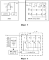
Figure 1 is a schematic diagram of a connection relation between an existing printing and imaging device and a consumable chip; -
Figure 2 is a schematic structural diagram of a consumable chip according to an embodiment of the present disclosure; -
Figure 3 is a schematic structural diagram of a storage circuit in an existing consumable chip; and -
Figure 4 is a schematic structural diagram of a storage circuit according to an embodiment of the present disclosure. - The embodiments of the present disclosure are described in detail below in conjunction with the drawings and the embodiments, so as to fully understand and implement the implementation process of how the present disclosure solves the technical problem via technical means and achieves the technical effect. It is to be understood that the embodiments of the present disclosure and features of the embodiments of the present disclosure can be combined with each other as long as no conflict occurs, and a technical solution formed in this way falls within the scope of protection of the present disclosure.
- Also, multiple specific details are set forth in the specification for purposes of explanation, to provide throughout understanding of the embodiments of the present disclosure. However, it is apparent to those skilled in the art that the present disclosure can be implemented without the specific details here or the described specific ways.
- Some of the existing printing and imaging devices are configured to read information on a consumable chip or write information into the consumable chip by means of a connection way shown in
Figure 1 . As shown inFigure 1 , acurrent source 101 and avoltage source 102 are provided in the printing and imaging device. Normally, thevoltage source 102 has an output voltage of 16V and a drive current greater than 10mA; and thecurrent source 101 has a drive current of 1mA and a highest voltage amplitude of 15V. Under control of acontroller 103, aswitching switch 104 can switch to output a current source signal or a voltage source signal onto a signal line ID. - The signal line ID is connected to a
consumable chip 105. In a case that the printing and imaging device performs a read operation, the printing and imaging device outputs the current source signal onto the signal line ID, and detects a voltage on the signal line ID via an ADC106, so as to read out data stored in the consumable chip. In a case that the printing and imaging device performs a write operation, the printing and imaging device outputs the voltage source signal onto the signal line ID, so as to write data to be written into the consumable chip. - To solve the problem that the existing consumable chip is unable to directly communicate with the printing and imaging device in a case that non-volatile memory (for example, the flash memory) easy to be rewritten is adopted as the memory unit, the present disclosure provides a new resistor switching circuit and a storage circuit and a consumable chip which include the resistor switching circuit.
-
Figure 2 is a schematic structural diagram of a consumable chip according to the embodiment. As shown inFigure 2 , the consumable chip according to the embodiment includes an operation instruction generation circuit 201 and astorage circuit 202. Specifically, the operation instruction generation circuit 201 is configured to identify whether a voltage source signal or a current source signal is transmitted on a signal line ID, that is, whether a voltage source or a current source is connected with the signal line ID in the printing and imaging device. In a case that the voltage source signal is transmitted on the signal line ID, the operation instruction generation circuit 201 outputs a write instruction WR; or in a case that the current source signal is transmitted on the signal line ID, the operation instruction generation circuit 201 outputs a read instruction RD. - In the embodiment, the operation instruction generation circuit 201 includes one input terminal for receiving a signal transmitted on the signal line ID and two output terminals. The two output terminals include a read instruction output terminal RD and a write instruction output terminal WR. Therefore, the operation instruction generation circuit in the embodiment is also referred to as a RD/WR identification circuit.
- In the consumable chip according to the embodiment, the
storage circuit 202 includes aresistor switching circuit 203, adata storage module 204 and a read/write control circuit 205. The read/write control circuit 205 is connected with thedata storage module 204 and the operation instruction generation circuit 201, and is configured to perform a read/write operation on a corresponding address of thedata storage module 204 based on address data that is received and an operation instruction that is generated by the operation instruction generation circuit 201. - Specifically, in a case that the operation instruction generation circuit 201 generates a write instruction, the read/
write control circuit 205 writes data into corresponding address space of thedata storage module 204; and in a case that the operation instruction generation circuit 201 generates a read instruction, the read/write control circuit 205 controls thedata storage module 204 to output data stored in corresponding address space to theresistor switching circuit 203. - In different embodiments of the present disclosure, in the
data storage module 204, a memory (for example, an EEPROM, a ferroelectric memory, a phase change memory, a flash memory and the like) easy to be programmed and erased may be adopted as the memory unit, or a combination (for example, an SRAM having a battery and the like) of an volatile memory and a power supply may be adopted as the memory unit, which is not limited in the present disclosure. In the embodiment, information stored in thedata storage module 204 includes consumable-cartridge identification information, a manufacturer, a production date, ink usage amount, ink remaining amount, a toner color and so on. Of course, in other embodiments of the present disclosure, the information stored in thedata storage module 204 may include some of the information described above, or may further include other reasonable information not listed, which is not limited in the present disclosure. - The read instruction output terminal RD and the write instruction output terminal WR each output a high-level signal or a low-level signal. In the embodiment, the high-level signal is defined as an effective signal. That is, in a case that the read instruction output terminal RD outputs the high-level signal, it indicates that a read instruction is effective. In a case that the write instruction output terminal WR outputs the high-level signal, it indicates that a write instruction is effective.
- The effective signal outputted by the operation instruction generation circuit 201 only includes two signals, that is, either the read instruction or the write instruction is effective. In other embodiments of the present disclosure, the two output terminals can be integrated into one output terminal in the operation instruction generation circuit 201. For example, in a case that a high-level signal is outputted by the output terminal, it is defined that the write instruction is effective; and in a case that a low-level signal is outputted by the output terminal, it is defined that the read instruction is effective. In this way, the
storage circuit 202 only has one input port to receive the read/write instruction, and does not require two ports to respectively receive the read instruction and the write instruction, thereby not only simplifying a circuit structure of the data storage circuit, but also simplifying an analysis processing process of the read/write instruction by the data storage circuit, and therefore improving read/write efficiency for data. - In a case that the operation instruction generation circuit 201 outputs a high-level signal at the read instruction output terminal RD, it indicates that the printing and imaging device is to read out data stored in the consumable chip. The printing and imaging device reads out the data by detecting a voltage on the signal line ID. In this case, the
storage circuit 202 of the consumable chip outputs data at a target address of thestorage circuit 202 to theresistor switching circuit 203 based on received address information. - In response to the read instruction, the
resistor switching circuit 203 selects a resistance value by means of a switch based on the data outputted by the data storage circuit. Theresistor switching circuit 203 also receives a current source signal outputted by the signal line ID. Since the current source signal flows through the selected resistance value in theresistor switching circuit 203, voltage drop is generated. The digital-to-analog converter ADC in the printing and imaging device can detect a voltage on the signal line ID, thereby reading the data. - Different resistance values can be obtained by reasonably combining resistance values in the resistor switching circuit. For example, in the embodiment, the combined resistance values in the resistor switching circuit include 1.5kΩ, 4kΩ, 7kΩ and an infinite value, which are four resistance values between a source electrode and a drain electrode in an EPROM circuit in the conventional technology.
- As mentioned above, the consumable chip in the embodiment determines an intention of the printing and imaging device based on the signal outputted by the printing and imaging device on the signal line ID. In a case that a current source signal is transmitted on the signal line ID, the consumable chip determines that the printing and imaging device is to perform a read operation; and in a case that a voltage source signal is transmitted on the signal line ID, the consumable chip determines that the printing and imaging device is to perform a write operation (for example, a programming operation).
- The non-volatile memory (for example, the flash memory) easy to be rewritten is not directly suitable for the printing and imaging device which accesses data of the consumable chip through the voltage source and the current source. The operation instruction generation circuit in the embodiment may generate a corresponding operation instruction (for example, the read instruction and the write instruction) based on the voltage source signal or the current source signal, so that the non-volatile memory easy to be rewritten can be installed and used in the printing and imaging device.
- In a case that the operation instruction generation circuit identifies that the ID signal is the current source signal, that is, an effective signal inputted to the storage circuit is the read signal, the consumable chip feedbacks information at a target address to the printing and imaging device based on the read signal and the address information that is received from the printing and the imaging device.
- The existing printing and imaging device reads information on the consumable chip by a connection way shown in
Figure 3 . A current source I and a voltage source U are provided in the printing and imaging device. Specifically, the voltage source U has an output voltage of 16V, and a drive current greater than 10 ma; and current source I has a drive current of 1mA, and a highest voltage amplitude of 15V. Under control of a controller, a switch K may be used to switch to output a current source signal or a voltage source signal onto the signal line ID. - The signal line ID is connected with an EPROM (Electrically Programmable Read-Only-Memory) storage circuit of the consumable chip. The EPROM storage circuit illustratively includes four information bits, that is, FGI, FG2, FG3 and FG4. Specifically, the bit FG1 is a reference bit, and is set to be un-programmable. The bit FG2 has been programmed completely, and a resistance value between a drain electrode and a source electrode is very large (equivalent to an open circuit). Each of the bits FG3 and FG4 is a stacked-gate injection MOS (Stacked-gate Injection Metal Oxide Semiconductor).
- The consumable chip receives address information sent by a printer (a transmission path for the address information is not shown in
Figure 3 ), and selects a bit to be accessed through a word line WL (Word Line) and a bit line BL (Bit Line) after decoding. A source electrode of the selected bit is connected with a low level. - For example, in a case that the printer is to program the bit FG4 (normally it is defined that the programming is to write "1", and information "1" is stored in the programmed SIMOS), the printer outputs a voltage source signal on the signal line ID, and selects the bit FG4 through the word line WL and the bit line BL.
- Since a control gate electrode and a drain electrode of the bit FG4 have a high voltage of 16V, and a source electrode thereof has a low level, a programming condition for the SIMOS is met, and avalanche breakdown occurs in a PN junction between the drain electrode of FG4 and a substrate. High-energy electrons generated by the avalanche breakdown passes through a silicon oxide insulation layer of the control gate electrode under effect of a gate electric field, to inject into a floating gate. After the electrodes are injected into the floating gate, a turn-on voltage (also referred to as a threshold voltage) of the SIMOS is raised.
- In order to access the EPROM storage circuit, the printer outputs a current source signal on the signal line ID, and selects a bit pointed by address information through the word line WL and the bit line BL. In this case, the digital-to-analog converter ADC (analog to digital converter) provided within the printer may detect a voltage on the signal line ID. The printer can determine a value read in the EPROM storage circuit based on the voltage value.
- For example, in a case that the printer is to read data in the bit FG3, since the FG3 is not programmed (it is defined that information "0" is stored in FG3), a turn-on voltage of the bit FG3 is low, a resistance value between a drain electrode and a source electrode of FG3 is low (approximately 1.5kΩ). In this case, a voltage detected on the signal line ID by the printer is approximately 1.5V.
- Similarly, in a case that the printer is to access the bit FG4, since the bit FG4 is programmed, a turn-on voltage of the bit FG4 is raised, and a resistance value between a drain electrode and a source electrode of the FG4 is increased (approximately 7kΩ). In this case, a voltage detected on the signal line ID by the printer is approximately 7V.
- In a case that the printer is to access the reference bit FG1, a resistance value between a drain electrode and a source electrode of FG1 is a value (for example, 4kΩ) between a value in a case of being programmed and a value in a case of being un-programmed. In this case, a voltage detected on the signal line ID by the printer is approximately 4V.
- In a case that the printer is to access the bit FG2, since FG2 is equivalent to an open circuit, a voltage detected on the signal line ID by the printer is the highest voltage amplitude (i.e., 15V) outputted by the current source.
- It can be seen that, in a case that the printer is to access the consumable chip, the analog-to-digital converter, ADC will read four signals having different voltage values instead of only a high-level signal or a low-level signal.
- In a case that the non-volatile memory (for example, the flash memory) is adopted to store data in the consumable chip, the consumable chip is unable to be directly suitable for the printing and imaging device which accesses the consumable chip through the voltage source/current source. This is because that read/write operation performed on the memory in the consumable chip is realized by adding a read indication code or a write indication code to an instruction, and the consumable chip represents whether "0" or "1" is read out by outputting a high-level signal or a low-level signal.
- For the problem described above, a novel resistor switching circuit is provided according to the present disclosure, for reading corresponding data in the data storage module.
Figure 4 is a schematic structural diagram of a storage circuit according to an embodiment. - As shown in
Figure 4 , in the embodiment, an input terminal of a read/write control circuit 205 includes a read instruction receiving port RD, a write instruction receiving port WR and an address information receiving port Add. In addition, the read/write control circuit further includes some interfaces (for example, a series data port SDA and a series clock port SCK using the IIC protocol) for purposes of production and processing, to program and erase a memory array. - The
resistor switching circuit 203 includes adecoder 203a and fourresistance switching branches 203b. The four resistance switching branches have a same structure. Each of the four resistance switching branches includes a switching switch and a resistor which are connected in series in a conductive loop of a signal line. Specifically, as shown inFigure 4 , in the embodiment, a first resistance switching branch includes a resistor R5 and a transistor K1. The resistor R5 is connected between the signal line ID and a source electrode of the transistor K1, a gate electrode of the transistor K1 is connected with a corresponding port of thedecoder 203a, and a drain electrode of the transistor K1 is grounded. A second resistance switching branch, a third resistance switching branch and a fourth resistance switching branch each have a same structure as the structure of the first resistance switching branch, and the only difference is that the four resistance switching branches have the resistors with different resistance values. In the embodiment, the resistance values of the resistors (that is, from a resistor R1 to a resistor R4) increases gradually from the first resistance switching branch to a fourth resistance switching branch. - The
decoder 203a is connected with adata storage module 204, and is configured to generate a switching instruction based on a signal outputted by thedata storage module 204, to control the switching switch of a respective one of the resistance switching branches to connect the resistor corresponding to the switching switch to the conductive loop of the signal line ID (that is, to turn on the resistance switching branch), so as to change a resistance value in the conductive loop of the signal line ID. - As shown in
Figure 4 , in a case that thestorage circuit 202 uses two bits to represent information stored in an SIMOS of the EPROM, theresistor switching circuit 203 includes a resistor array including resistors R5, R6, R7 and R8 and transistors K1, K2, K3 and K4 connected with the resistors R5, R6, R7 and R8 respectively to serve as a switch, and a 2/4 decoder. - In the embodiment, resistance values of the four resistors are 1.5kΩ, 4kΩ, 7kΩ and 10MΩ, respectively. As described above, in a case that 00 represents "0", 01 represents a reference bit, 10 represents "1" and 11 represents a bit having a large resistance value, the 2/4
decoder 203a associates 00 outputted by thedata storage module 204 with the switching switch K1, associates 01 outputted by thedata storage module 204 with the switching switch K2, associates 10 outputted by thedata storage module 204 with the switching switch K3 and associates 11 outputted by thedata storage module 204 with the switching switch K4. - In a case that the address information indicates that SIMOS programmed is to be read, data 10, i.e., "1", is stored at an address of the
data storage module 204 corresponding to the address information. In this case, the read/write control circuit 205 controls thedata storage module 204 to output the data 10 stored therein to the 2/4decoder 203a. The 2/4decoder 203a outputs a high level at a gate electrode of the switching switch K3 to turn on the switching switch K3, to select the third resistor R7, and other switching switches are turned off in this case. Since the resistance value of the third resistor R7 is 7kΩ. A dividing voltage of 7V is generated on the resistor R7 by the current source signal, and a voltage of the signal line ID is 7V. The voltage is detected by the ADC in the printing and imaging device, to read the data "1". - Practically, in other embodiments of the present disclosure, bit values in the memory array corresponding to data "0" and data "1" may be other reasonable values, and the number of output terminals of the decoder and the number of resistance switching branches may be adjusted , which is not limited in the present disclosure. For example, in an embodiment of the present disclosure, 000 represents "0", and 111 represents "1"; and in this case, eight resistance switching branches may be provided and a 3/8 decoder may be used.
- It should be illustrated that, in other embodiments of the present disclosure, the storage circuit of the consumable chip may include multiple resistor switching circuits. Each of the multiple resistor switching circuits is connected with the
data storage module 204, which is not limited in the present disclosure. - It can be seen from above that, in the existing printing and imaging device, the consumable chip is accessed through the voltage source/current source, and the EPROM storage circuit is used in the consumable chip. Since the EPROM storage circuit can be wrote only once, it is not convenient to maintain or recycle the consumable chip in such printing and imaging device.
- The resistor switching circuit is provided in the embodiment, which is particularly suitable for the non-volatile memory easy to be rewritten. Such non-volatile memory easy to be rewritten represents whether "0" or "1" is read out by outputting a high level or a low level in response to a read instruction, and the level is unable to match with the printing and imaging device normally. The resistor switching circuit according to the embodiments changes a resistance value in the conductive loop of the signal line based on a level signal outputted by the memory, so as to change a voltage of the signal line. In this way, the printing and imaging device can acquire data at a corresponding address of the memory by detecting the voltage on the signal line. The consumable chip including the resistor switching circuit can be modified easily and is suitable for the printing and imaging device which accesses the data of the consumable chip through a voltage source or a current source, thereby facilitating maintenance of the consumable chip and improving the recycle efficiency.
- "An embodiment" or "embodiments" mentioned in the specification refers to that the specific features, structures or characteristics described in conjunction with the embodiment are included in at least one embodiment of the present disclosure. Therefore, a phrase "an embodiment" or "embodiments" everywhere in the specification does not necessarily refer to the same one embodiment.
- Although the examples described above are used to illustrate a principle of the present disclosure in one or more applications, various modifications can be made to forms, usages or implementation details by those skilled in the art without creative work and without departing the principle and concept of the present disclosure. Therefore, the present disclosure is limited by the appended claims.
Claims (4)
- A chip (105) comprised in a consumable cartridge for containing coloring materials, wherein the chip (105) is connected to a printing and imaging device via a signal line ID; the printing and imaging device comprises a current source (101) for transmitting a current source signal on the signal line ID; the chip comprises an operation instruction generation circuit (201) and a storage circuit (202); and the storage circuit (202) further comprises a data storage module (204), a read/write control circuit (205) and a resistor switching circuit (203), wherein:the operation instruction generation circuit (201) is connected with the signal line ID and configured to generate and output a read instruction to the read/write control circuit (205), based on the current source signal transmitted on the signal line ID;the data storage module (204) is configured to store data associated with the consumable cartridge for containing coloring materials, and the data storage module (204) comprises any one of an EEPROM memory, a ferroelectric memory, a phase change memory, a flash memory, and a volatile memory connected with a power supply;the read/write control circuit (205) is connected with the data storage module (204) and configured to, based on the read instruction generated by the operation instruction generation circuit (201) and address data that is received, control the data storage module (204) to output data; andthe resistor switching circuit (203) is configured to change a resistance value in a conductive loop of the signal line ID based on data outputted by the data storage module (204), wherein the resistor switching circuit (203) comprises:a plurality of resistance switching branches, wherein each of the plurality of resistance switching branches comprises a switching switch (K1, K2, K3 or K4) and a resistor (R5, R6, R7, or R8) which are connected in series in the conductive loop of the signal line ID; anda decoder (203a) connected with the data storage module (204) and configured to generate a switching instruction based on data outputted by the data storage module (204), to control the switching switch (K1, K2, K3 or K4) of a respective one of the resistance switching branches to connect the resistor (R5, R6, R7, or R8) corresponding to the switching switch (K1, K2, K3 or K4) to the conductive loop of the signal line ID, so as to change a resistance value in the conductive loop of the signal line ID, wherein the current source signal flows through the resistance value and generates voltage drop.
- The chip (105) according to claim 1, wherein the resistor switching circuit (203) comprises four resistance switching branches, with resistance values of resistors (R5, R6, R7, or R8) in the four resistance switching branches being different from each other and increasing gradually from a first resistance switching branch to a fourth resistance switching branch.
- The chip (105) according to claim 2, wherein the decoder (203a) is a 2/4 decoder.
- The chip (105) according to claim 3, wherein the decoder (203a) is configured to:generate a switching instruction to connect the resistor in the first resistance switching branch to the conductive loop of the signal line ID, in a case that data received by the decoder (203a) is "00";generate a switching instruction to connect the resistor in a second resistance switching branch to the conductive loop of the signal line, in a case that data received by the decoder (203a) is "01";generate a switching instruction to connect the resistor in a third resistance switching branch to the conductive loop of the signal line, in a case that data received by the decoder (203a) is "10"; orgenerate a switching instruction to connect the resistor in the fourth resistance switching branch to the conductive loop of the signal line, in a case that data received by the decoder (203a) is "11".
Applications Claiming Priority (3)
| Application Number | Priority Date | Filing Date | Title |
|---|---|---|---|
| CN201410715520 | 2014-11-28 | ||
| CN201510317377.4A CN104952485B (en) | 2014-11-28 | 2015-06-10 | A kind of resistance switching circuit, storage circuit and consumable chip |
| PCT/CN2015/095536 WO2016082760A1 (en) | 2014-11-28 | 2015-11-25 | Resistor switching circuit, storage circuit, and consumable chip |
Publications (3)
| Publication Number | Publication Date |
|---|---|
| EP3109864A1 EP3109864A1 (en) | 2016-12-28 |
| EP3109864A4 EP3109864A4 (en) | 2017-07-26 |
| EP3109864B1 true EP3109864B1 (en) | 2019-04-24 |
Family
ID=54158682
Family Applications (1)
| Application Number | Title | Priority Date | Filing Date |
|---|---|---|---|
| EP15863566.4A Active EP3109864B1 (en) | 2014-11-28 | 2015-11-25 | Resistor switching circuit, storage circuit, and consumable chip |
Country Status (5)
| Country | Link |
|---|---|
| US (2) | US9633701B2 (en) |
| EP (1) | EP3109864B1 (en) |
| CN (2) | CN104943395B (en) |
| ES (1) | ES2735751T3 (en) |
| WO (2) | WO2016082760A1 (en) |
Families Citing this family (13)
| Publication number | Priority date | Publication date | Assignee | Title |
|---|---|---|---|---|
| CN104943395B (en) * | 2014-11-28 | 2016-08-31 | 珠海艾派克微电子有限公司 | A kind of operational order generative circuit and consumable chip |
| CN113589045B (en) * | 2018-01-17 | 2024-09-20 | 珠海极海半导体有限公司 | Sensitive resistor measuring device and measuring method |
| CN109263287B (en) * | 2018-08-15 | 2020-01-31 | 珠海艾派克微电子有限公司 | RC switching circuit, electric storage device and printing material replacement part |
| CN109334261B (en) * | 2018-10-09 | 2023-12-29 | 杭州旗捷科技有限公司 | Instruction generation circuit, consumable chip and consumable |
| CN112100117A (en) * | 2019-06-18 | 2020-12-18 | 北京小米移动软件有限公司 | Power supply multiplexing circuit, data signal switching method and device and electronic equipment |
| CN112259138A (en) * | 2019-07-22 | 2021-01-22 | 森富科技股份有限公司 | Memory device |
| CN111016465B (en) * | 2019-12-24 | 2021-09-07 | 珠海艾派克微电子有限公司 | A chip and imaging cartridge |
| CN113442597B (en) * | 2019-12-31 | 2022-12-23 | 极海微电子股份有限公司 | Consumable chip, response method of consumable chip, consumable box and storage medium |
| CN111806095B (en) * | 2020-07-20 | 2021-09-07 | 珠海艾派克微电子有限公司 | Consumables remaining quantity detection method, consumables, and image forming apparatus |
| CN111817284B (en) * | 2020-09-04 | 2021-01-19 | 深圳市永联科技股份有限公司 | Direct current bus communication circuit and method |
| CN113110119B (en) * | 2020-11-26 | 2022-08-19 | 国网天津市电力公司 | Electronic type full-automatic branch exchanger |
| CN113203921A (en) * | 2020-11-26 | 2021-08-03 | 国网天津市电力公司 | One-key type full-automatic tester for insulation standardization between branches |
| CN113848415A (en) * | 2021-01-28 | 2021-12-28 | 江西理工大学 | IRF generator, generation method of fault resistance and IRF injection method |
Citations (1)
| Publication number | Priority date | Publication date | Assignee | Title |
|---|---|---|---|---|
| US20050259123A1 (en) * | 2004-02-13 | 2005-11-24 | Hugh Rice | Device identification using a programmable memory circuit |
Family Cites Families (19)
| Publication number | Priority date | Publication date | Assignee | Title |
|---|---|---|---|---|
| JPH08235875A (en) | 1994-12-27 | 1996-09-13 | Nkk Corp | Multilevel information storage device and operating method thereof |
| US5602925A (en) * | 1995-01-31 | 1997-02-11 | Etymotic Research, Inc. | Hearing aid with programmable resistor |
| US6655775B1 (en) * | 1996-10-15 | 2003-12-02 | Hewlett-Packard Development Company, L.P. | Method and apparatus for drop weight encoding |
| JP3133706B2 (en) * | 1997-06-19 | 2001-02-13 | 三洋電機株式会社 | Nonvolatile semiconductor memory device |
| ES2231266T3 (en) * | 1999-10-04 | 2005-05-16 | Seiko Epson Corporation | INTEGRATED CIRCUIT, INK CARTRIDGE AND INK BLACK PRINTER. |
| JP4081963B2 (en) * | 2000-06-30 | 2008-04-30 | セイコーエプソン株式会社 | Storage device and access method for storage device |
| CN1280102C (en) * | 2003-03-14 | 2006-10-18 | 国际联合科技股份有限公司 | Burning method of identification circuit of inkjet printing head |
| US20050062584A1 (en) * | 2003-09-24 | 2005-03-24 | Broadcom Corporation | High-linearity switched-resistor network for programmability |
| KR100725979B1 (en) * | 2005-07-23 | 2007-06-08 | 삼성전자주식회사 | Apparatus and method for improving write / read durability of nonvolatile memory |
| DE102005043489B4 (en) | 2005-09-13 | 2009-07-23 | Abb Ag | Automation device |
| ES2403304T3 (en) * | 2007-11-14 | 2013-05-17 | Hewlett-Packard Development Company, L.P. | An inkjet printhead with shared data lines |
| US8599424B2 (en) * | 2008-09-04 | 2013-12-03 | Fb Sistemas S.A. | Printer cartridge microchip |
| KR101047051B1 (en) * | 2009-05-20 | 2011-07-06 | 주식회사 하이닉스반도체 | Nonvolatile Semiconductor Memory Circuit |
| US8284589B2 (en) * | 2010-08-20 | 2012-10-09 | Sandisk 3D Llc | Single device driver circuit to control three-dimensional memory element array |
| US8787068B2 (en) * | 2011-04-07 | 2014-07-22 | Elpida Memory, Inc. | Semiconductor device |
| CN202332456U (en) | 2011-11-29 | 2012-07-11 | 上海贝岭股份有限公司 | Numerical control rheostat based on weighing switching network |
| KR20140080942A (en) * | 2012-12-21 | 2014-07-01 | 에스케이하이닉스 주식회사 | Non-volatile memory apparatus |
| CN203191538U (en) * | 2013-04-12 | 2013-09-11 | 昆明理工大学 | Numerical control resistance box of binary resistor |
| CN104943395B (en) * | 2014-11-28 | 2016-08-31 | 珠海艾派克微电子有限公司 | A kind of operational order generative circuit and consumable chip |
-
2015
- 2015-06-10 CN CN201510317365.1A patent/CN104943395B/en active Active
- 2015-06-10 CN CN201510317377.4A patent/CN104952485B/en active Active
- 2015-11-25 WO PCT/CN2015/095536 patent/WO2016082760A1/en not_active Ceased
- 2015-11-25 WO PCT/CN2015/095537 patent/WO2016082761A1/en not_active Ceased
- 2015-11-25 US US15/122,722 patent/US9633701B2/en active Active
- 2015-11-25 EP EP15863566.4A patent/EP3109864B1/en active Active
- 2015-11-25 US US15/528,925 patent/US9865314B2/en active Active
- 2015-11-25 ES ES15863566T patent/ES2735751T3/en active Active
Patent Citations (1)
| Publication number | Priority date | Publication date | Assignee | Title |
|---|---|---|---|---|
| US20050259123A1 (en) * | 2004-02-13 | 2005-11-24 | Hugh Rice | Device identification using a programmable memory circuit |
Also Published As
| Publication number | Publication date |
|---|---|
| CN104952485B (en) | 2019-07-19 |
| CN104943395A (en) | 2015-09-30 |
| WO2016082761A1 (en) | 2016-06-02 |
| US20170330604A1 (en) | 2017-11-16 |
| CN104943395B (en) | 2016-08-31 |
| WO2016082760A1 (en) | 2016-06-02 |
| EP3109864A1 (en) | 2016-12-28 |
| CN104952485A (en) | 2015-09-30 |
| EP3109864A4 (en) | 2017-07-26 |
| US9633701B2 (en) | 2017-04-25 |
| US20170069357A1 (en) | 2017-03-09 |
| US9865314B2 (en) | 2018-01-09 |
| ES2735751T3 (en) | 2019-12-20 |
Similar Documents
| Publication | Publication Date | Title |
|---|---|---|
| US9633701B2 (en) | Resistor switching circuit, storage circuit, and consumable chip | |
| US8144525B2 (en) | Memory cell sensing using negative voltage | |
| US9824766B2 (en) | Semiconductor device including nonvolatile memory configured to switch between a reference current reading system and a complementary reading system | |
| KR101618063B1 (en) | Non-volatile semiconductor memory device and method of reading the same | |
| US8913436B2 (en) | Non-volatile memory (NVM) with word line driver/decoder using a charge pump voltage | |
| TW200710678A (en) | Apparatus and method for reading an array of nonvolatile memory cells including switchable resistor memory elements | |
| US9263145B2 (en) | Current detection circuit and semiconductor memory apparatus | |
| CN113678202B (en) | ReRAM memory cell with dual wordline control | |
| US20150303922A1 (en) | High voltage switch circuit and nonvolatile memory including the same | |
| US8289776B2 (en) | Expanded programming window for non-volatile multilevel memory cells | |
| CN210606643U (en) | Resistive random access memory | |
| JP2009283118A (en) | Program method of nonvolatile memory device | |
| CN105931669A (en) | Semiconductor device | |
| US7355903B2 (en) | Semiconductor device including memory cells and current limiter | |
| CN109102835A (en) | non-volatile semiconductor storage device and reading method thereof | |
| KR970008166A (en) | Semiconductor nonvolatile memory device and computer system using the same | |
| CN103794248B (en) | The control grid word line driver circuit of multigrid tube memory | |
| WO2007062378A2 (en) | Array source line (avss) controlled high voltage regulation for programming flash or ee array | |
| US9336868B1 (en) | Common plate switching reduction in resistive switching memory devices | |
| US9224486B1 (en) | Control gate driver for use with split gate memory cells | |
| KR101310075B1 (en) | Single-Poly Multi-Time Programmable memory | |
| JPH10334073A (en) | One-chip microcomputer | |
| JP2009259351A (en) | Nonvolatile storage device and control method of nonvolatile storage device | |
| KR20160099455A (en) | Systems, devices and methods for memory operations | |
| CN104750584A (en) | Semiconductor storing device and system starting method |
Legal Events
| Date | Code | Title | Description |
|---|---|---|---|
| PUAI | Public reference made under article 153(3) epc to a published international application that has entered the european phase |
Free format text: ORIGINAL CODE: 0009012 |
|
| STAA | Information on the status of an ep patent application or granted ep patent |
Free format text: STATUS: REQUEST FOR EXAMINATION WAS MADE |
|
| 17P | Request for examination filed |
Effective date: 20160921 |
|
| AK | Designated contracting states |
Kind code of ref document: A1 Designated state(s): AL AT BE BG CH CY CZ DE DK EE ES FI FR GB GR HR HU IE IS IT LI LT LU LV MC MK MT NL NO PL PT RO RS SE SI SK SM TR |
|
| AX | Request for extension of the european patent |
Extension state: BA ME |
|
| A4 | Supplementary search report drawn up and despatched |
Effective date: 20170622 |
|
| RIC1 | Information provided on ipc code assigned before grant |
Ipc: H03M 11/24 20060101ALI20170616BHEP Ipc: G11C 16/10 20060101AFI20170616BHEP Ipc: B41J 2/175 20060101ALI20170616BHEP |
|
| DAV | Request for validation of the european patent (deleted) | ||
| DAX | Request for extension of the european patent (deleted) | ||
| STAA | Information on the status of an ep patent application or granted ep patent |
Free format text: STATUS: EXAMINATION IS IN PROGRESS |
|
| 17Q | First examination report despatched |
Effective date: 20180515 |
|
| GRAP | Despatch of communication of intention to grant a patent |
Free format text: ORIGINAL CODE: EPIDOSNIGR1 |
|
| STAA | Information on the status of an ep patent application or granted ep patent |
Free format text: STATUS: GRANT OF PATENT IS INTENDED |
|
| INTG | Intention to grant announced |
Effective date: 20181114 |
|
| GRAS | Grant fee paid |
Free format text: ORIGINAL CODE: EPIDOSNIGR3 |
|
| GRAA | (expected) grant |
Free format text: ORIGINAL CODE: 0009210 |
|
| STAA | Information on the status of an ep patent application or granted ep patent |
Free format text: STATUS: THE PATENT HAS BEEN GRANTED |
|
| AK | Designated contracting states |
Kind code of ref document: B1 Designated state(s): AL AT BE BG CH CY CZ DE DK EE ES FI FR GB GR HR HU IE IS IT LI LT LU LV MC MK MT NL NO PL PT RO RS SE SI SK SM TR |
|
| REG | Reference to a national code |
Ref country code: GB Ref legal event code: FG4D |
|
| REG | Reference to a national code |
Ref country code: CH Ref legal event code: EP |
|
| REG | Reference to a national code |
Ref country code: AT Ref legal event code: REF Ref document number: 1125088 Country of ref document: AT Kind code of ref document: T Effective date: 20190515 Ref country code: IE Ref legal event code: FG4D |
|
| REG | Reference to a national code |
Ref country code: DE Ref legal event code: R096 Ref document number: 602015029107 Country of ref document: DE |
|
| REG | Reference to a national code |
Ref country code: NL Ref legal event code: FP |
|
| REG | Reference to a national code |
Ref country code: LT Ref legal event code: MG4D |
|
| PG25 | Lapsed in a contracting state [announced via postgrant information from national office to epo] |
Ref country code: PT Free format text: LAPSE BECAUSE OF FAILURE TO SUBMIT A TRANSLATION OF THE DESCRIPTION OR TO PAY THE FEE WITHIN THE PRESCRIBED TIME-LIMIT Effective date: 20190824 Ref country code: SE Free format text: LAPSE BECAUSE OF FAILURE TO SUBMIT A TRANSLATION OF THE DESCRIPTION OR TO PAY THE FEE WITHIN THE PRESCRIBED TIME-LIMIT Effective date: 20190424 Ref country code: AL Free format text: LAPSE BECAUSE OF FAILURE TO SUBMIT A TRANSLATION OF THE DESCRIPTION OR TO PAY THE FEE WITHIN THE PRESCRIBED TIME-LIMIT Effective date: 20190424 Ref country code: NO Free format text: LAPSE BECAUSE OF FAILURE TO SUBMIT A TRANSLATION OF THE DESCRIPTION OR TO PAY THE FEE WITHIN THE PRESCRIBED TIME-LIMIT Effective date: 20190724 Ref country code: FI Free format text: LAPSE BECAUSE OF FAILURE TO SUBMIT A TRANSLATION OF THE DESCRIPTION OR TO PAY THE FEE WITHIN THE PRESCRIBED TIME-LIMIT Effective date: 20190424 Ref country code: HR Free format text: LAPSE BECAUSE OF FAILURE TO SUBMIT A TRANSLATION OF THE DESCRIPTION OR TO PAY THE FEE WITHIN THE PRESCRIBED TIME-LIMIT Effective date: 20190424 Ref country code: LT Free format text: LAPSE BECAUSE OF FAILURE TO SUBMIT A TRANSLATION OF THE DESCRIPTION OR TO PAY THE FEE WITHIN THE PRESCRIBED TIME-LIMIT Effective date: 20190424 |
|
| PG25 | Lapsed in a contracting state [announced via postgrant information from national office to epo] |
Ref country code: RS Free format text: LAPSE BECAUSE OF FAILURE TO SUBMIT A TRANSLATION OF THE DESCRIPTION OR TO PAY THE FEE WITHIN THE PRESCRIBED TIME-LIMIT Effective date: 20190424 Ref country code: PL Free format text: LAPSE BECAUSE OF FAILURE TO SUBMIT A TRANSLATION OF THE DESCRIPTION OR TO PAY THE FEE WITHIN THE PRESCRIBED TIME-LIMIT Effective date: 20190424 Ref country code: GR Free format text: LAPSE BECAUSE OF FAILURE TO SUBMIT A TRANSLATION OF THE DESCRIPTION OR TO PAY THE FEE WITHIN THE PRESCRIBED TIME-LIMIT Effective date: 20190725 Ref country code: BG Free format text: LAPSE BECAUSE OF FAILURE TO SUBMIT A TRANSLATION OF THE DESCRIPTION OR TO PAY THE FEE WITHIN THE PRESCRIBED TIME-LIMIT Effective date: 20190724 Ref country code: LV Free format text: LAPSE BECAUSE OF FAILURE TO SUBMIT A TRANSLATION OF THE DESCRIPTION OR TO PAY THE FEE WITHIN THE PRESCRIBED TIME-LIMIT Effective date: 20190424 |
|
| REG | Reference to a national code |
Ref country code: AT Ref legal event code: MK05 Ref document number: 1125088 Country of ref document: AT Kind code of ref document: T Effective date: 20190424 |
|
| REG | Reference to a national code |
Ref country code: ES Ref legal event code: FG2A Ref document number: 2735751 Country of ref document: ES Kind code of ref document: T3 Effective date: 20191220 |
|
| PG25 | Lapsed in a contracting state [announced via postgrant information from national office to epo] |
Ref country code: IS Free format text: LAPSE BECAUSE OF FAILURE TO SUBMIT A TRANSLATION OF THE DESCRIPTION OR TO PAY THE FEE WITHIN THE PRESCRIBED TIME-LIMIT Effective date: 20190824 |
|
| REG | Reference to a national code |
Ref country code: DE Ref legal event code: R097 Ref document number: 602015029107 Country of ref document: DE |
|
| PG25 | Lapsed in a contracting state [announced via postgrant information from national office to epo] |
Ref country code: DK Free format text: LAPSE BECAUSE OF FAILURE TO SUBMIT A TRANSLATION OF THE DESCRIPTION OR TO PAY THE FEE WITHIN THE PRESCRIBED TIME-LIMIT Effective date: 20190424 Ref country code: EE Free format text: LAPSE BECAUSE OF FAILURE TO SUBMIT A TRANSLATION OF THE DESCRIPTION OR TO PAY THE FEE WITHIN THE PRESCRIBED TIME-LIMIT Effective date: 20190424 Ref country code: CZ Free format text: LAPSE BECAUSE OF FAILURE TO SUBMIT A TRANSLATION OF THE DESCRIPTION OR TO PAY THE FEE WITHIN THE PRESCRIBED TIME-LIMIT Effective date: 20190424 Ref country code: AT Free format text: LAPSE BECAUSE OF FAILURE TO SUBMIT A TRANSLATION OF THE DESCRIPTION OR TO PAY THE FEE WITHIN THE PRESCRIBED TIME-LIMIT Effective date: 20190424 Ref country code: RO Free format text: LAPSE BECAUSE OF FAILURE TO SUBMIT A TRANSLATION OF THE DESCRIPTION OR TO PAY THE FEE WITHIN THE PRESCRIBED TIME-LIMIT Effective date: 20190424 Ref country code: SK Free format text: LAPSE BECAUSE OF FAILURE TO SUBMIT A TRANSLATION OF THE DESCRIPTION OR TO PAY THE FEE WITHIN THE PRESCRIBED TIME-LIMIT Effective date: 20190424 |
|
| PG25 | Lapsed in a contracting state [announced via postgrant information from national office to epo] |
Ref country code: SM Free format text: LAPSE BECAUSE OF FAILURE TO SUBMIT A TRANSLATION OF THE DESCRIPTION OR TO PAY THE FEE WITHIN THE PRESCRIBED TIME-LIMIT Effective date: 20190424 |
|
| PLBE | No opposition filed within time limit |
Free format text: ORIGINAL CODE: 0009261 |
|
| STAA | Information on the status of an ep patent application or granted ep patent |
Free format text: STATUS: NO OPPOSITION FILED WITHIN TIME LIMIT |
|
| PG25 | Lapsed in a contracting state [announced via postgrant information from national office to epo] |
Ref country code: TR Free format text: LAPSE BECAUSE OF FAILURE TO SUBMIT A TRANSLATION OF THE DESCRIPTION OR TO PAY THE FEE WITHIN THE PRESCRIBED TIME-LIMIT Effective date: 20190424 |
|
| 26N | No opposition filed |
Effective date: 20200127 |
|
| PG25 | Lapsed in a contracting state [announced via postgrant information from national office to epo] |
Ref country code: SI Free format text: LAPSE BECAUSE OF FAILURE TO SUBMIT A TRANSLATION OF THE DESCRIPTION OR TO PAY THE FEE WITHIN THE PRESCRIBED TIME-LIMIT Effective date: 20190424 |
|
| REG | Reference to a national code |
Ref country code: CH Ref legal event code: PL |
|
| PG25 | Lapsed in a contracting state [announced via postgrant information from national office to epo] |
Ref country code: LI Free format text: LAPSE BECAUSE OF NON-PAYMENT OF DUE FEES Effective date: 20191130 Ref country code: CH Free format text: LAPSE BECAUSE OF NON-PAYMENT OF DUE FEES Effective date: 20191130 Ref country code: MC Free format text: LAPSE BECAUSE OF FAILURE TO SUBMIT A TRANSLATION OF THE DESCRIPTION OR TO PAY THE FEE WITHIN THE PRESCRIBED TIME-LIMIT Effective date: 20190424 Ref country code: LU Free format text: LAPSE BECAUSE OF NON-PAYMENT OF DUE FEES Effective date: 20191125 |
|
| REG | Reference to a national code |
Ref country code: BE Ref legal event code: MM Effective date: 20191130 |
|
| PG25 | Lapsed in a contracting state [announced via postgrant information from national office to epo] |
Ref country code: IE Free format text: LAPSE BECAUSE OF NON-PAYMENT OF DUE FEES Effective date: 20191125 |
|
| PG25 | Lapsed in a contracting state [announced via postgrant information from national office to epo] |
Ref country code: BE Free format text: LAPSE BECAUSE OF NON-PAYMENT OF DUE FEES Effective date: 20191130 |
|
| PG25 | Lapsed in a contracting state [announced via postgrant information from national office to epo] |
Ref country code: CY Free format text: LAPSE BECAUSE OF FAILURE TO SUBMIT A TRANSLATION OF THE DESCRIPTION OR TO PAY THE FEE WITHIN THE PRESCRIBED TIME-LIMIT Effective date: 20190424 |
|
| PG25 | Lapsed in a contracting state [announced via postgrant information from national office to epo] |
Ref country code: MT Free format text: LAPSE BECAUSE OF FAILURE TO SUBMIT A TRANSLATION OF THE DESCRIPTION OR TO PAY THE FEE WITHIN THE PRESCRIBED TIME-LIMIT Effective date: 20190424 Ref country code: HU Free format text: LAPSE BECAUSE OF FAILURE TO SUBMIT A TRANSLATION OF THE DESCRIPTION OR TO PAY THE FEE WITHIN THE PRESCRIBED TIME-LIMIT; INVALID AB INITIO Effective date: 20151125 |
|
| PG25 | Lapsed in a contracting state [announced via postgrant information from national office to epo] |
Ref country code: MK Free format text: LAPSE BECAUSE OF FAILURE TO SUBMIT A TRANSLATION OF THE DESCRIPTION OR TO PAY THE FEE WITHIN THE PRESCRIBED TIME-LIMIT Effective date: 20190424 |
|
| REG | Reference to a national code |
Ref country code: DE Ref legal event code: R081 Ref document number: 602015029107 Country of ref document: DE Owner name: GEEHY MICROELECTRONICS INC., ZHUHAI, CN Free format text: FORMER OWNER: APEX MICROELECTRONICS CO., LTD, ZHUHAI, GUANGDONG, CN Ref country code: DE Ref legal event code: R082 Ref document number: 602015029107 Country of ref document: DE Representative=s name: DENNEMEYER & ASSOCIATES S.A., DE Ref country code: DE Ref legal event code: R082 Ref document number: 602015029107 Country of ref document: DE Representative=s name: DENNEMEYER & ASSOCIATES RECHTSANWALTSGESELLSCH, DE |
|
| P01 | Opt-out of the competence of the unified patent court (upc) registered |
Effective date: 20230530 |
|
| REG | Reference to a national code |
Ref country code: NL Ref legal event code: PD Owner name: GEEHY MICROELECTRONICS INC.; CN Free format text: DETAILS ASSIGNMENT: CHANGE OF OWNER(S), CHANGE OF LEGAL ENTITY; FORMER OWNER NAME: APEX MICROELECTRONICS CO., LTD Effective date: 20231103 |
|
| REG | Reference to a national code |
Ref country code: ES Ref legal event code: PC2A Owner name: GEEHY MICROELECTRONICS INC. Effective date: 20241014 |
|
| REG | Reference to a national code |
Ref country code: DE Ref legal event code: R082 Ref document number: 602015029107 Country of ref document: DE Representative=s name: DENNEMEYER & ASSOCIATES RECHTSANWALTSGESELLSCH, DE |
|
| PGFP | Annual fee paid to national office [announced via postgrant information from national office to epo] |
Ref country code: NL Payment date: 20251119 Year of fee payment: 11 |
|
| PGFP | Annual fee paid to national office [announced via postgrant information from national office to epo] |
Ref country code: DE Payment date: 20251119 Year of fee payment: 11 |
|
| PGFP | Annual fee paid to national office [announced via postgrant information from national office to epo] |
Ref country code: GB Payment date: 20251120 Year of fee payment: 11 |
|
| PGFP | Annual fee paid to national office [announced via postgrant information from national office to epo] |
Ref country code: IT Payment date: 20251125 Year of fee payment: 11 |
|
| PGFP | Annual fee paid to national office [announced via postgrant information from national office to epo] |
Ref country code: FR Payment date: 20251126 Year of fee payment: 11 |
|
| PGFP | Annual fee paid to national office [announced via postgrant information from national office to epo] |
Ref country code: ES Payment date: 20251229 Year of fee payment: 11 |