EP3104455B1 - Dipole-shaped radiator assembly - Google Patents
Dipole-shaped radiator assembly Download PDFInfo
- Publication number
- EP3104455B1 EP3104455B1 EP16172969.4A EP16172969A EP3104455B1 EP 3104455 B1 EP3104455 B1 EP 3104455B1 EP 16172969 A EP16172969 A EP 16172969A EP 3104455 B1 EP3104455 B1 EP 3104455B1
- Authority
- EP
- European Patent Office
- Prior art keywords
- radiator
- dipole
- line
- support
- halves
- Prior art date
- Legal status (The legal status is an assumption and is not a legal conclusion. Google has not performed a legal analysis and makes no representation as to the accuracy of the status listed.)
- Active
Links
- 239000000758 substrate Substances 0.000 claims description 25
- 230000008878 coupling Effects 0.000 claims description 10
- 238000010168 coupling process Methods 0.000 claims description 10
- 238000005859 coupling reaction Methods 0.000 claims description 10
- 238000011144 upstream manufacturing Methods 0.000 claims description 3
- 230000007704 transition Effects 0.000 claims 2
- 230000010287 polarization Effects 0.000 description 71
- 239000004020 conductor Substances 0.000 description 45
- 239000002184 metal Substances 0.000 description 7
- 238000005192 partition Methods 0.000 description 6
- 239000000463 material Substances 0.000 description 4
- 239000000969 carrier Substances 0.000 description 3
- 238000005476 soldering Methods 0.000 description 3
- 230000005540 biological transmission Effects 0.000 description 2
- 230000015572 biosynthetic process Effects 0.000 description 2
- 238000010276 construction Methods 0.000 description 2
- 230000009977 dual effect Effects 0.000 description 2
- 230000010363 phase shift Effects 0.000 description 2
- 230000006978 adaptation Effects 0.000 description 1
- 238000003491 array Methods 0.000 description 1
- 238000005452 bending Methods 0.000 description 1
- 238000005266 casting Methods 0.000 description 1
- 238000010586 diagram Methods 0.000 description 1
- 238000007688 edging Methods 0.000 description 1
- 230000000694 effects Effects 0.000 description 1
- 238000009434 installation Methods 0.000 description 1
- 238000004080 punching Methods 0.000 description 1
- 230000005855 radiation Effects 0.000 description 1
- 230000000630 rising effect Effects 0.000 description 1
- 238000007493 shaping process Methods 0.000 description 1
Images


Classifications
-
- H—ELECTRICITY
- H01—ELECTRIC ELEMENTS
- H01Q—ANTENNAS, i.e. RADIO AERIALS
- H01Q9/00—Electrically-short antennas having dimensions not more than twice the operating wavelength and consisting of conductive active radiating elements
- H01Q9/04—Resonant antennas
- H01Q9/16—Resonant antennas with feed intermediate between the extremities of the antenna, e.g. centre-fed dipole
- H01Q9/28—Conical, cylindrical, cage, strip, gauze, or like elements having an extended radiating surface; Elements comprising two conical surfaces having collinear axes and adjacent apices and fed by two-conductor transmission lines
- H01Q9/285—Planar dipole
-
- H—ELECTRICITY
- H01—ELECTRIC ELEMENTS
- H01Q—ANTENNAS, i.e. RADIO AERIALS
- H01Q1/00—Details of, or arrangements associated with, antennas
- H01Q1/50—Structural association of antennas with earthing switches, lead-in devices or lightning protectors
-
- H—ELECTRICITY
- H01—ELECTRIC ELEMENTS
- H01Q—ANTENNAS, i.e. RADIO AERIALS
- H01Q1/00—Details of, or arrangements associated with, antennas
- H01Q1/12—Supports; Mounting means
- H01Q1/22—Supports; Mounting means by structural association with other equipment or articles
- H01Q1/24—Supports; Mounting means by structural association with other equipment or articles with receiving set
- H01Q1/241—Supports; Mounting means by structural association with other equipment or articles with receiving set used in mobile communications, e.g. GSM
- H01Q1/246—Supports; Mounting means by structural association with other equipment or articles with receiving set used in mobile communications, e.g. GSM specially adapted for base stations
-
- H—ELECTRICITY
- H01—ELECTRIC ELEMENTS
- H01Q—ANTENNAS, i.e. RADIO AERIALS
- H01Q1/00—Details of, or arrangements associated with, antennas
- H01Q1/36—Structural form of radiating elements, e.g. cone, spiral, umbrella; Particular materials used therewith
-
- H—ELECTRICITY
- H01—ELECTRIC ELEMENTS
- H01Q—ANTENNAS, i.e. RADIO AERIALS
- H01Q1/00—Details of, or arrangements associated with, antennas
- H01Q1/48—Earthing means; Earth screens; Counterpoises
-
- H—ELECTRICITY
- H01—ELECTRIC ELEMENTS
- H01Q—ANTENNAS, i.e. RADIO AERIALS
- H01Q19/00—Combinations of primary active antenna elements and units with secondary devices, e.g. with quasi-optical devices, for giving the antenna a desired directional characteristic
- H01Q19/10—Combinations of primary active antenna elements and units with secondary devices, e.g. with quasi-optical devices, for giving the antenna a desired directional characteristic using reflecting surfaces
- H01Q19/12—Combinations of primary active antenna elements and units with secondary devices, e.g. with quasi-optical devices, for giving the antenna a desired directional characteristic using reflecting surfaces wherein the surfaces are concave
-
- H—ELECTRICITY
- H01—ELECTRIC ELEMENTS
- H01Q—ANTENNAS, i.e. RADIO AERIALS
- H01Q21/00—Antenna arrays or systems
- H01Q21/24—Combinations of antenna units polarised in different directions for transmitting or receiving circularly and elliptically polarised waves or waves linearly polarised in any direction
-
- H—ELECTRICITY
- H01—ELECTRIC ELEMENTS
- H01Q—ANTENNAS, i.e. RADIO AERIALS
- H01Q9/00—Electrically-short antennas having dimensions not more than twice the operating wavelength and consisting of conductive active radiating elements
- H01Q9/04—Resonant antennas
- H01Q9/16—Resonant antennas with feed intermediate between the extremities of the antenna, e.g. centre-fed dipole
- H01Q9/18—Vertical disposition of the antenna
-
- H—ELECTRICITY
- H01—ELECTRIC ELEMENTS
- H01Q—ANTENNAS, i.e. RADIO AERIALS
- H01Q9/00—Electrically-short antennas having dimensions not more than twice the operating wavelength and consisting of conductive active radiating elements
- H01Q9/04—Resonant antennas
- H01Q9/16—Resonant antennas with feed intermediate between the extremities of the antenna, e.g. centre-fed dipole
- H01Q9/28—Conical, cylindrical, cage, strip, gauze, or like elements having an extended radiating surface; Elements comprising two conical surfaces having collinear axes and adjacent apices and fed by two-conductor transmission lines
Definitions
- the invention relates to a dipole radiator arrangement according to claim 1.
- Dipole radiators are for example from the Vorveröttingungen DE 197 22 742 A such as DE 196 27 015 A known.
- Such dipole radiators can have a conventional dipole structure in the form of a simple dipole or consist for example of a crossed dipole or a dipole square, etc.
- a so-called vector dipole is eg from the pre-publication WO 00/39894 A1 known. Its structure seems to be comparable to a dipole square.
- due to the specific design of the dipole radiator according to this prior publication and the special feed of this dipole radiator acts much like a cross dipole, which radiates in two polarization planes perpendicular to each other. In constructive In particular, it is rather square because of its outer contour design.
- Such dipole radiators are usually fed in such a way that a dipole or radiator half is DC-connected (ie galvanically) to an outer conductor, whereas the inner conductor of a coaxial connecting cable is connected to the second dipole or radiator half in a DC manner (ie in turn galvanically).
- the feed takes place in each case at the mutually facing end portions of the dipole or radiator halves.
- the support means or the respectively associated half of the support means of the radiator arrangement can therefore also capacitively coupled to ground at its base or at its base to ground or galvanically connected to the reflector and thereby be grounded.
- such single- or dual-polarized emitters can also have a very broadband design so that they can transmit and / or receive in different frequency ranges or frequency bands.
- radiators can usually be superimposed in one or more antenna columns.
- Such antenna arrays can also be controlled, for example using phase shifters, in particular differential phase shifters, with different phase, so that a different down-angle can be set.
- phase shifters in particular differential phase shifters, with different phase, so that a different down-angle can be set.
- a possible arrangement using multiple-phase shifters for different setting of a down-tilt angle with corresponding supply of dual-polarized radiators is for example from EP 2 406 851 B1 refer to.
- the feed is usually asymmetrical using a coaxial cable, which thus comprises a cable structure with a signal line and a ground line.
- a single-polarized dipole radiator is usually fed by means of a coaxial cable, wherein the outer conductor of the coaxial cable is soldered at the inner end of one of the radiator halves approximately at the level of the radiator halves, ie in particular the dipole halves.
- the inner conductor is passed over it, to the adjacent inner end of the second radiator half, i. in the specific case of the second dipole half, where the inner conductor forming the signal line is soldered.
- a corresponding supply also takes place via a coaxial conductor for each of the two polarization planes, as explained above.
- a dipole-shaped radiator is further from the US 2003/0193377 A1 known.
- the publication describes a feed point at the dipole point. Via the network, a specific signal is generated at the feed station.
- the mentioned MEM switches are arranged. This makes it possible to realize a switching of the supply, which leads to a 180 ° phase shift. This is equivalent to a reversal of the current flow in the feed of the dipole.
- the object of the present invention is now to provide an improved feed structure on the basis of such a prior art.
- a significantly improved feed structure is created in a surprising manner, which is not only advantageous on its own, but also opens up a number of advantageous application possibilities.
- asymmetrical feed structure for example using a coaxial cable, for which at least one plane of polarization is fed twice.
- a double-feed can be realized for the preferably two polarization planes.
- a ground conductor is not only galvanically or optionally also capacitively coupled to the one radiator half and the associated signal conductor on the opposite radiator half, but that next to it a second feed structure is provided.
- This second radiator structure is basically the same or similar, but the ground conductor of the second feed structure preferably at the inner end of those Hallower half is galvanically or capacitively connected, to which the signal or inner conductor of the first feed structure is coupled. Conversely, the signal or inner conductor of the second feed structure is continued beyond the ground conductor to the second radiator half belonging to the same plane of polarization and there coupled galvanically or capacitively, ie with the radiator half, in which the ground conductor of the first feed structure is coupled.
- the ground connection to the radiator device can also take place in a region below the actual radiator halves or dipole halves. for example, at the level of the base of the support means of the radiator structure.
- This double feed allows, for example, that the same physical radiator for two different frequency ranges can be fed via different upstream phase shifters. This makes it possible in the simplest way to operate the same physical radiator, for example, in two different frequency bands and these frequency bands via upstream phase shifter different in their down-tilt range or to change this lowering angle.
- This improvement can be realized without additional increase in the required installation space on the reflector back of such a radiator arrangement or such a radiator array. Because today's generation of particular intended for mobile antennas is fitted on the back of the reflector usually provided with a variety of components, so that there is hardly any free space available.
- the inventively proposed feed structure requires only that from the back of the reflector, via corresponding passages or holes, the corresponding unbalanced lines to the radiator side of the reflector, ie to the so-called front or front side are passed, up to the corresponding coupling points where the signal lines and the ground lines are coupled to the respective radiator halves.
- the invention also opens up the possibility that the aforementioned asymmetrical radiator structure can be implemented in a simple manner not only using coaxial cables, but also using another, two-line feed system, for example in the form of a micro-strip line, a coplanar line arrangement , an arrangement using single or multilayer boards which are part of the dipole structure and which on the preferably opposite side to the electrically conductive surface of Carrying device of the radiator structure and / or the radiator or dipole structure itself are provided with the aforementioned micro-strip line, which is once designed as a ground line and once as a signal line.
- FIG. 1 is a schematic plan view of an antenna array, that is shown in the concrete, a single-column antenna array 1, which is usually mounted extending in the vertical direction.
- This antenna array 1 comprises a reflector 3, which in a vertical plan view in FIG FIG. 1 is shown.
- V of the antenna array 1 are generally mounted at equidistant intervals A radiator 5 (distance A between two neighboring in the V direction centers of two radiators).
- FIG. 1 For example, two single-polarized radiators 5a arranged at a distance from one another in the direction V are reproduced, whose two dipole radiator halves 7.1a and 7.1b are aligned transversely and in particular perpendicular to the vertical or longitudinal direction V.
- an associated, perpendicular to the reflector plane RE extending polarization plane P1 is defined, which in FIG. 1 is shown in dashed lines and perpendicular to the reflector plane RE and thus perpendicular to the plane.
- a dipole-shaped cross-radiator 5b is shown for clarity, and a so-called vector radiator 5c is again offset, having two polarization planes P1 and P2 oriented perpendicular to one another.
- An equally usable dipole square is not shown for clarity, but could be used as well.
- radiators 5a are simply polarized dipole radiators
- the in FIG. 1 represented Dipolnch 5b and the vector dipole 5c in two mutually perpendicular polarization planes P1 and P2 send and / or can receive, as well as, for example, in a correspondingly aligned dipole square.
- the actual radiator elements i. the dipole halves 7.1a and 7.1b with singly polarized radiators and the radiator halves 7.1a, 7.1b and 7.2a, 7.2b in dual polarized radiators usually extend at a distance from the reflector 3 in parallel alignment with the reflector plane RE.
- radiators are only examples in FIG. 1 to clarify that an antenna array 1 can be constructed using a variety of radiators 5a, 5b and / or 5c, ie using emitters of the same type or of radiators with different designs.
- the structures can thus be different, whereby differently shaped radiators can be used, which radiate in different bands.
- vector emitters 5c these can be designed in a very broadband fashion so that they can transmit and / or receive in at least two or even several mutually offset frequency bands.
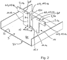
- FIG. 2 is a corresponding spatial representation of the in FIG. 1 shown antenna array, but only under a simplified view of a simple dipole radiator 5a, which radiates only in a polarization plane P1.
- Such dipole-shaped radiators usually have a carrier 11 which, in the case of a dipole radiator 2, comprises carrier halves 11.1a and 11.1b which extend from the reflector plane RE of the reflector 3 to the level of the dipole halves 7.1a and 13b extending laterally away from one another 7.1b, with the formation of a slit 13.1 provided therebetween, which in the case of a dipole can also be referred to as Symmetri mecanicsschlitz 13.1.
- the dipole halves 7.1a and 7.1b are separated from each other at the level of the radiators via the mentioned slot 13.1, and thus have adjacent to each other so-called inner Strahlerendabroughe 107, i. 107.1a and 107.1b and removes lying outwardly facing Strahlerendabête 117.1a and 117.1b, which are hereinafter also referred to as outer Strahlerendabchae 117.1a, 117.1b.
- Such a dipole or generally dipole radiator may be made of a conductive metal, such as a casting.
- a corresponding dipole for example a crossed dipole, may also consist of a sheet metal part or be made of a sheet metal part which can be shaped accordingly by tilting, punching, edging and / or bending.
- dipole radiators can also be made, for example, using a dielectric, e.g. be formed in the form of a single or multi-layer board or using a corresponding board material, which at least on one side, i. the front or the back is covered with a metallized layer. Preferably, the entire surface is metallized accordingly.
- the slot 13.1 extends, as mentioned, almost over the entire height of the dipole or may deviate in the illustrated embodiment FIG. 2 one below to the reflector 3 lying, the two carrier halves 11.1a and 11.1b connecting connecting web 15.1 have, whereby the entire common base 17 of the carrier 11.1 and thus the base 17 of the radiator 5 is formed.
- This connecting web 15.1 is one of the possible variants in FIG. 2 drawn only by dashed lines, since the radiator halves 7.1a and 7.1b can also extend to the reflector plane RE through the slot 13 separately.
- connection of the underside of the carrier 11.1 or the carrier halves 11.1a, 11.1b with or without additional connecting web 15.1 preferably be realized by means of a galvanic contacting with the conductive reflector 3 , but also possible here is the formation of a capacitive connection. If an insulating intermediate layer between the base 17, so the bottom of the base 17 (with or without in FIG. 2 shown connecting web 15.1) and the electrically conductive reflector layer is provided, thereby generating a capacitive coupling of the respective radiator on the reflector 3. In other words, a capacitive or, if necessary, a galvanic connection to the reflector can be provided here on the base 17 of the carrier 11.
- the feed height or the eating plane SpE is usually provided, which in FIG. 2 is shown in dashed form, this plane is parallel to the reflector plane RE.
- this feed height or feed level the feeding of the transmission signals or the received signals, which is explained in detail below, usually takes place.
- the feed can certainly be provided in a certain range even below the height range in which the dipole or radiator halves 7.1a, 7.1b are formed.
- the radiator height H with respect to the reflector plane RE and thus more or less the length of the slot 13.1 generally correspond to a value of about ⁇ / 4.
- the radiator height and / or the slot length should preferably not fall below a value of ⁇ / 10.
- the radiator height could basically be an arbitrary multiple of ⁇ (especially since a radiator has a radiation diagram even without a reflector).
- ⁇ preferably represents a wavelength from the frequency band to be transmitted, preferably in a middle frequency of the band to be transmitted. If it is a broadband radiator transmitting two or more frequency bands, the value of ⁇ should preferably be a mean size of the entire frequency band range from the lowest to the highest value of the different frequency bands.
- FIG. 3a is a schematic side view, in FIG. 3b in spatial view and in Figure 3c in plan view a section of the dipole radiator 7.1 according to FIG. 1 and 2 reproduced, namely with its two carrier halves 11.1a, 11.1b and the lower connecting web 15, without the running away at the upper end of the carrier 11.1 dipole or radiator halves 7.1a, 7.1b, the only in FIG. 3a are indicated.
- such a dipole radiator is fed asymmetrically, using a two-line feed 21.1, 21.1a, e.g. in the form of an asymmetrical coaxial cable 121.1a, which is guided from the underside or rear side of the reflector 3 via a recess or bore in the reflector 3 to the radiator side and then along a support half, for example, the carrier half 11.1a towards the top lying end of the carrier 11.1 out running is.
- a two-line feed 21.1, 21.1a e.g. in the form of an asymmetrical coaxial cable 121.1a, which is guided from the underside or rear side of the reflector 3 via a recess or bore in the reflector 3 to the radiator side and then along a support half, for example, the carrier half 11.1a towards the top lying end of the carrier 11.1 out running is.
- the upper end of the ground conductor 25.1 in the case of a coaxial cable 125a in the form of an outer conductor 125.1a, can be capacitively and preferably galvanically connected, in particular by soldering, to the electrically conductive surface of the adjacent carrier half 11a, ie, for example at a ground feeding point 126.1a.
- the outer conductor of the in FIGS. 3a to 3c shown coaxial cable 125.1 still surrounded by an insulating outer sheath, which leads to the vicinity of the feed point 126.1a, where the then exposed outer conductor is soldered to the upper end of the carrier of the radiator.
- This insulating outer sheath is not shown in the figures for the sake of simplicity.
- ⁇ represents, however, as a rule and preferably the mean wavelength of the frequency band to be transmitted.
- the signal line 27.1 extends, here in the form of an inner conductor 127.1a of the coaxial cable 121.1a, wherein the inner conductor is also passed over the slot 13 and capacitively or galvanically connected to the opposite portion of the other dipole or radiator half 7.1b.
- the connection should be done galvanically, for example by means of soldering.
- the signal coupling takes place via the signal line here in the form of the inner conductor 27.1a at a signal feed point 128.1b at the top and inner region of the second carrier half 11b.
- the supply carried out at there formed dining points or points 126.1a and 128.1b, by at the one dining place 126.1a of the ground conductor 25.1a and at the other feed point 126.1b of the signal conductor 27.1a is connected galvanically or capacitively.
- FIGS. 3a to 3c But how about the FIGS. 3a to 3c It can also be seen, in the context of the invention to the same radiator or dipole 5 still a second feed 21.1b is provided, which is formed exactly the opposite of the first.
- the second two-line feed 21.1b may be provided, for example in the form of another coaxial cable 121.1b, which, for example, on the second carrier half 11.1b from the back of the reflector via a bore in the outer or inner reflector in the upper direction End of the carrier 11.1 is designed to extend.
- the associated ground conductor 25.1b in the form of the associated outer conductor 125.1b is in turn capacitively or galvanically connected to the associated carrier 11.1b in the region of the overhead feed point 126.1b and thus capacitively or galvanically connected to the associated dipole or radiator half 7.1b
- the signal line 27.1b, here in the form of the inner conductor 127.1b over the slot 13 away in the reverse direction to the inner conductor 127.1a of the first two-line feed 21.1a to the opposite portion of the carrier half 11.1a and thus to the inner feed point 128.1a at the inner radiator end portion 107.1a of the associated dipole or radiator half 7.1a running trained and connected there galvanically or capacitively.
- the same radiator 5 can be operated, for example, in two different frequency ranges, wherein the one frequency band in the transmitting and / or receiving direction via the one two-line feed 21.1a, here in the form of coaxial cable 121.1a, and another Two-line feed 21.1b can be done for example for a second frequency range via the second coaxial cable 121.1b.
- the peculiarity is that the two coaxial cables 121.1a and 121.1b can be preceded by different phase adjustment devices, for example in the form of phase shifters and in particular differential phase shifters, so that the different frequency ranges that transmit and receive via the same radiators 5 are different and different from each other separate down-tilt angles can be easily adjusted.
- the coaxial cables 121.1a, 121.1b arranged with their ground or outer conductors and their inner or signal conductors on the same side of the associated dipole or radiator 5, for example on the in the FIGS. 3a and 3b Therefore, the two outer conductors 125.1a and 125.1b terminate in slightly different height H1 or H2 with respect to the reflector plane RE, ie the underside of the base 17.1, so that the lines can be mounted without collision.
- this is a coaxial two-line feed system 21.1a, for example formed on the first or front side 31 of the preferably perpendicular to the reflector plane RE rising Stahlers or dipole, whereas the second two-line feeder 21.1b is formed on the opposite second or rear side 32 of the dipole or radiator 5, ie in plan view of a about a leading through the center of the radiator and perpendicular to the reflector plane RE central axis rotated by 180 ° alignment and arrangement.
- the feed points 126.1a and 126.1b for the ground or outer conductors of the two coaxial cables 121.1a and 121.1b as well as the feed points 128.1b and 128.1a for the inner or signal conductors 27.1a, 27.1b are usually on same height level H1, although here, too, a certain height difference would be quite possible.
- this embodiment is a cross-shaped dipole radiator 5b which transmits and receives in two mutually perpendicular polarization planes P1 and P2.
- the further difference to the previous embodiment is that the unbalanced two-line system 21.1 and 21.1b is realized not by means of coaxial cable 121, but by using microstrip lines 221 (strip lines).
- the cross-shaped radiator 5b comprises two perpendicular dipoles 7.1 and 7.2, each with two in the associated plane of polarization P1, P2 dipole or radiator halves 7.1a, 7.1b and 7.2a, 7.2b, wherein the polarization planes P1 , P2, as in the first embodiment also, are aligned perpendicular to the reflector plane RE according to the design of the radiator.
- the two polarization planes P1 and P2 intersect at the center of the radiators such that the two dipole halves 7.1a, 7.1b lie in the first polarization plane P1 and the two perpendicular radiator or dipole halves 7.2a, 7.2b in the second polarization plane P2.
- Each of the carriers 11.1 and 11.2 lying parallel to the planes of polarization P1, P2 with the associated carrier halves 11.1a and 11.1b or 11.2a, 11.2b can be made of metal or metal plates, in particular of one or more assembled sheet metal parts. It is also possible that these carriers are formed, for example, from printed circuit board material, ie from a dielectric, wherein at least one and preferably both of the opposite side surfaces are coated with an electrically conductive layer, which are preferably galvanically connected to one another.
- the paired carrier halves 11.1a, 11.1b and 11.2a, 11.2b which are perpendicular to each other with respect to both polarization planes P1, P2, can be mounted and / or held on a common base 17, with which they are preferably also electrically connected , Via a provided for example in the middle of the base 17 bore 18 then the base as well as the radiator can be connected in total galvanic or capacitive as explained with an electrically conductive reflector, whereby it is electrically connected and mechanically held accordingly.
- the two feed systems are basically similar and similar to the previous embodiment.
- connection of a ground line 25 (as generally based on FIGS. 3a and 3b already described), ie in the present case, the connection of a ground line 25.1a, 25.1b or 25.2a, 25.2b, for example via the galvanic connection of the lower end of the carrier 11, ie the respective carrier halves 11.1a, 11.1b and 11.2a, 11.2b not only directly, but also for example via the electrically conductive base 17 with the reflector 3 and / or a separate mass Connection lead (which in the FIGS. 5a to 5e not shown).
- a galvanic or capacitive connection of the ground line for example in the vicinity of the upper portions of a carrier half 11.1a, 11.1b and 11.2a, 11.2b are performed, as based on FIGS. 3a to 4c explained.
- the in the embodiment according to FIGS. 5a to 5e respectively provided two signal lines 27.1a, 27.1b and 27.2a, 27.2b (of which, due to the illustration, only the signal lines located on one side of the carrier halves 27.1a and 27.2a are visible) are in this embodiment preferably each as a micro-strip -Leitung (ie as a strip line) 221.a, 221b and 221.2a, 221.2b formed, so as a conductor on a corresponding dielectric 128, for example in the form of a printed circuit board material 128, which thus serves as a substrate or support, here in specific as a support plate.
- a micro-strip -Leitung ie as a strip line
- the design of the respective ground line 25.1a, 25.1b and 25.2a, 25.2b in microstrip form 221.1a, 221.1b or 221.2a, 221.2b designed in a lateral plan view in the manner of an inverted L or approximately L-shaped designed, including the associated Carrier or the substrate 128 may be designed with appropriate shape but can not.
- This printed circuit board material 128 with the microstrip feed or signal line 27.1, 27.2 thereon is in each case in parallel contact with the actual plate-shaped carrier 11, for each polarization P1 or P2. the respective carrier half 11.1 or 11.2, for each polarization in the form of the carrier half 11.1a, 11.1b or 11.2a, 11.2b adjacent or provided at a small distance.
- the electrically conductive surface of the carrier 11 serves as a ground plane for the spaced apart by the thickness of the substrate 128 to the micro-strip conductor track.
- the signal lines 27.1a, 27.1b and 27.2a, 27.2b are preferably respectively facing outward on the associated non-conductive surface of the carrier 11.
- an associated ground surface may be formed on the immediate, opposite rear side of the substrate 128 for forming the microstrip interconnects, which is preferably separated from the ground plane of the carrier halves with the interposition of a dielectric film or with the interposition of an air gap.
- the structure is, for example, for the polarization P1 such that the corresponding in the form of an inverted L approximate support structure is positioned in the form of the carrier 128 with the conductor thereon 127.1a in abutment on one side 31 of the associated carrier halves, for the first feed system 21.1a.
- the intended for the same plane of polarization second feed system 21.1b is preferably arranged on the opposite side of the same carrier half, so that the feed is formed inversely for each polarization, as described with reference to FIGS. 4a to 4c for a coaxial cable feed.
- the feed takes place in microstrip form for the second polarization P2, so that two feed systems 21.1a, 21.1b and 21.2a, 21.2b for the first polarization plane P1 and two feed systems for the second polarization plane P2 are present.
- the respective plate-shaped dielectric support (substrate) 128 preferably has a tongue 128a projecting at the lower end, wherein the signal or conductor track 27.1a, 27.1b, 27.2a, 27.2b provided on the plate-shaped dielectric support 128 extends into the region of the projecting tongue 128a is formed running.
- the respective conductor track 27 terminates preferably in the region of this protruding tongue 128a, which preferably protrudes in the mounted state via a bore or recess in the reflector 3 from the radiator or front side to the rear side of the reflector, so that there the corresponding end 27th 'of the signal conductor 27.1a, 27.1b and 27.2a, 27.2b can be connected to a corresponding feed network (usually by soldering).
- the signal line in the form of the conductor path thus runs parallel to the underlying conductor track carrier section in the form of the mentioned dielectric 128 from the tongue 128a to the level of the overhead dipole or radiator section 7.1, 7.1b and 7.2a, 7.2b, then in a perpendicular to this line section to pass in the area the opposite dipole or radiator half in parallel alignment ends. In each case, this results in a capacitive coupling between the section of the microstrip line 221.1a, 221.1b or 221.2a, 221.2b, which is routed via the slot 13, for the two polarization planes.
- the corresponding connection of the respective second feed system for the first and second polarization plane takes place in a plan view perpendicular to the plane of the drawing according to FIG. 5d (ie parallel to the central axis Z lying centrally) by 180 ° in an identical manner (the central axis Z being perpendicular to the plane of the drawing in FIG FIG. 5d runs). That is, the two second signal lines of the second feed system extend on the respectively opposite and also outwardly facing sides of the respective other carrier portion, from its lower connection point to the level of the overhead dipole or radiator half. From there, they preferably extend at right angles to the opposite dipole radiator section and the coupling surface provided there.
- this ground surface can extend into the area of the tongue 128a (also there on the rear side to the end 27 ').
- the feed line 21) run, in order to then also be connected to ground at the appropriate point below the reflector plane RE, ie on the back of the reflector or in the region of the reflector itself.
- the microstrip lines could also be formed on the side of the substrate 128 facing the associated support section 11.1 or 11.2 of the associated dipole or radiator half, if in particular between this microstrip line and the associated ground plane of the carrier 11.1, 11.2 or the dipole or radiator surface nor an insulating intermediate layer is provided.
- a double feed system is provided for each polarization plane P1 and P2.
- the two feed lines for both polarization levels can end at about the same height.
- the corresponding dielectric carrier plates that is to say the substrate 128 on which the microstrip lines 221.1a, 221.1b for the one polarization plane P1 or 221.2a, 221.2b for the second polarization plane P2 are formed, are made even larger can be and still offer more space to larger sized Filter structures F and / or matching circuits F to realize.
- a vector dipole made from one or more sheet-metal parts can also be manufactured in the form of stamped parts, which is designed according to the invention. It is so far only exemplary of the pre-published DE 20 2005 015 708 U1 referred, from which a demér structure is basically to be taken as known. The signal or feed line to be taken there can then likewise be realized again in quasi double execution.
- FIGS. 7a to 7c a further embodiment is shown in exploded view, namely for a vector dipole 5, which basically has a cross-shaped radiator structure.
- the vector dipole can basically have a shape as they are only exemplary and in principle from the WO 2008/022703 A1 or the WO 2005/060049 A1 or one of the above-described and mentioned prior publications is dealt with.
- vector dipoles also radiate and receive in two mutually perpendicular planes of polarization P1 and P2, wherein the mutually perpendicular polarization planes each extend through the diagonal through a vector dipole.
- the two radiator halves provided for each plane of polarization are taken to be more square in plan view or approximate to a square of the basic structure.
- the support 11 here consists of four support quadrants 11.1a, 11.1b, 11.2a, 11.2b, which are arranged lying in plan view about the central central axis Z offset by 90 °.
- two adjacent carrier quadrants are separated from one another by a slot 13 extending from the base upwards and thus almost over the entire height of the beam.
- the carrier quadrants are connected to one another only via their underlying base 17, which extends only in a small partial height. It is also possible that the individual Suquadranten separated from each other directly electrically or capacitively electrically connected to the electrically conductive reflector and are mechanically fixed there.
- Each extending in the diagonal direction, ie congruent to two mutually perpendicular polarization planes P1, P2 are formed from the center Z outwardly extending U-shaped wall portions 43, the U-shaped connecting web facing outward, so that the four thus formed, in plan view to 90th ° offset U-shaped pocket-shaped receiving areas 45 converge in the middle to a common central space 46 or connected to it.
- the signal or feed lines 27 are described below in detail housed.
- each of the U-shaped pockets in plan view (which are closed to the outside and converge in the central central region to form a common space 46) are still separated from one another by a respective central partition wall 47.
- This partition is externally connected to the bottom-shaped web of the U-shaped receiving areas 45 in the illustrated embodiment.
- the opposite inwardly to the center indicative boundary edges of this partition 47 terminate at a distance from each other, so that there again the mentioned common central interior 46 is formed.
- each two feed systems for each of the two polarization planes can be introduced by a dielectric 128 can be inserted with thereon feed line for each polarization plane ,
- the respective two feed systems for both polarization planes P1 and P2 are preferably plate-shaped, wherein the signal lines are formed as micro-strip lines which run on corresponding dielectric carriers or substrates 128.
- a support or substrate plate 128.1 can be used for one polarization plane P1 in one of the subdivided U-shaped pockets, whereas the second support or substrate plate 128.2 belonging to the same plane of polarization is rotated through 180 ° into the center Z opposite to the one other side of the partition wall 47 formed chamber can be inserted.
- the respective horizontal line sections which terminate in the corresponding coupling sections, are arranged at a slightly different height for the one polarization plane than the two horizontal coupling and line sections with respect to the two further feed systems for the other polarization plane, so that in principle a structural design results, as it was made clear in itself with reference to the two preceding embodiments.
- connection stub 525 serving for galvanic ground connection preferably protrudes perpendicularly at the underside of the base.
- a coaxial, preferably galvanic connection to a ground line not shown in detail or a ground connection can preferably be made on the underside of the reflector via this connection stub.
- the connection stub 525 serving for the ground connection would be inserted through corresponding bores through the reflector.
- signal connection coupler 701 can be used, which can be plugged with suitable training directly on the counter to the beam direction of the radiator downwardly extending, free-ended signal lines.
- a double system is shown.
- two dipole-shaped vector radiators 5c which radiate in two polarization planes P1 and P2, are arranged on a common carrier plate 63 at a distance from one another.
- the vector dipoles therefore have respective receiving pockets 45 extending inward diagonally from the center Z, in each case diagonally to the approximately square outer contour of the vector radiator, in each of which the respective plate-shaped carrier (plate-shaped substrate or dielectric) passes into the two for each polarization plane P1 and P2 the partitions 47 can be used separate chambers.
- the illustrated signal line 27.1a, 27.1b, 27.2a, 27.2b is formed in each case on one side in the form of a microstrip line 221, so that for each polarization plane P1 and P2 two feed systems 21.1 and 21.2 are provided.
- the individual substrates i. the plate-shaped carrier 128 is designed for the two polarizations such that their upper coupling section extending across the respective slot 13 is provided at different altitudes A1 and A2 for the two polarizations, so that the corresponding micro-strip line sections intersect with respect to the two polarization planes can.
Landscapes
- Engineering & Computer Science (AREA)
- Computer Networks & Wireless Communication (AREA)
- Variable-Direction Aerials And Aerial Arrays (AREA)
- Aerials With Secondary Devices (AREA)
Description
Die Erfindung betrifft eine dipolförmige Strahleranordnung nach Anspruch 1.The invention relates to a dipole radiator arrangement according to
Dipolstrahler sind beispielsweise aus den Vorveröffentlichungen
Ein sogenannter Vektor-Dipol ist z.B. aus der Vorveröffentlichung
A so-called vector dipole is eg from the pre-publication
Aus der
Derartige Dipolstrahler werden üblicherweise so gespeist, dass eine Dipol- oder Strahlerhälfte mit einem Außenleiter gleichstrommäßig (also galvanisch) verbunden wird, wohingegen der Innenleiter eines koaxialen Anschlusskabels mit der zweiten Dipol- oder Strahlerhälfte gleichstrommäßig (also wiederum galvanisch) verbunden wird. Die Einspeisung erfolgt dabei jeweils an den aufeinander zu weisenden Endbereichen der Dipol- oder Strahlerhälften.Such dipole radiators are usually fed in such a way that a dipole or radiator half is DC-connected (ie galvanically) to an outer conductor, whereas the inner conductor of a coaxial connecting cable is connected to the second dipole or radiator half in a DC manner (ie in turn galvanically). The feed takes place in each case at the mutually facing end portions of the dipole or radiator halves.
Aus der
Derartige einfach- oder dualpolarisierte Strahler können gegebenenfalls auch sehr breitbandig ausgebildet sein, so dass sie in unterschiedlichen Frequenzbereichen oder Frequenzbändern senden und/oder empfangen können.If appropriate, such single- or dual-polarized emitters can also have a very broadband design so that they can transmit and / or receive in different frequency ranges or frequency bands.
Ferner können derartige Strahler üblicherweise in einer oder in mehreren Antennenspalten übereinander beabstandet sein. Derartige Antennenarrays können ferner beispielsweise unter Verwendung von Phasenschiebern, insbesondere Differenz-Phasenschiebern, so mit unterschiedlicher Phase angesteuert werden, dass sich ein unterschiedlicher Absenkwinkel (Down-Tilt-Winkel) einstellen lässt. Eine mögliche Anordnung unter Verwendung von Mehrfach-Phasenschiebern zur unterschiedlichen Einstellung eines Down-Tilt-Winkels mit entsprechender Anspeisung von dualpolarisierten Strahlern ist beispielsweise aus der
Unterschiedliche Ausführungsformen von dipolförmigen Antennen bzw. von kreuzförmigen Strahleranordnungen sind unter anderem auch aus der
Bei den erläuterten einfach- oder dualpolarisierten Strahlern erfolgt die Speisung üblicherweise unsymmetrisch unter Verwendung eines Koaxialkabels, welches also eine Kabelstruktur mit einer Signalleitung und einer Masseleitung umfasst.In the illustrated single- or dual-polarized radiators, the feed is usually asymmetrical using a coaxial cable, which thus comprises a cable structure with a signal line and a ground line.
Ein einfach-polarisierter Dipolstrahler wird dabei in der Regel mittels einer Koaxialleitung gespeist, wobei der Außenleiter des Koaxialkabels etwa in Höhe der Strahlerhälften, also insbesondere der Dipolhälften, an dem innenliegenden Ende einer der Strahlerhälften angelötet wird. Der Innenleiter wird darüber hinweg geführt, und zwar zu dem benachbarten innenliegenden Ende der zweiten Strahlerhälfte, d.h. in dem konkreten Fall der zweiten Dipolhälfte, wo der die Signalleitung bildende Innenleiter angelötet ist.A single-polarized dipole radiator is usually fed by means of a coaxial cable, wherein the outer conductor of the coaxial cable is soldered at the inner end of one of the radiator halves approximately at the level of the radiator halves, ie in particular the dipole halves. The inner conductor is passed over it, to the adjacent inner end of the second radiator half, i. in the specific case of the second dipole half, where the inner conductor forming the signal line is soldered.
Im Falle eines Kreuzdipols oder eines Vektordipols mit kreuzförmiger Struktur (also mit zwei senkrecht zueinander stehenden Polarisationsebenen) erfolgt ebenfalls für jede der beiden Polarisationsebenen eine entsprechende Einspeisung über einen Koaxialleiter, wie vorstehend erläutert.In the case of a cross dipole or a vector dipole with a cross-shaped structure (that is to say with two polarization planes perpendicular to one another), a corresponding supply also takes place via a coaxial conductor for each of the two polarization planes, as explained above.
Ein dipolförmiger Strahler ist ferner aus der
Eine insoweit vergleichbare Lösung ist auch aus der
Nur zur Vervollständigung soll noch angegeben werden, dass aus der
Auch bei der vorstehend genannten Vorveröffentlichung
Aufgabe der vorliegenden Erfindung ist es nunmehr, ausgehend von einem derartigen Stand der Technik eine verbesserte Speisestruktur zu schaffen.The object of the present invention is now to provide an improved feed structure on the basis of such a prior art.
Die Aufgabe wird erfindungsgemäß entsprechend den im Anspruch 1 angegebenen Merkmalen gelöst. Vorteilhafte Ausgestaltungen der Erfindung sind in den Unteransprüchen angegeben.The object is achieved according to the features specified in
Im Rahmen der vorliegenden Erfindung wird auf überraschende Weise eine deutlich verbesserte Speisestruktur geschaffen, die nicht nur für sich genommen vorteilhaft ist, sondern zudem eine Reihe vorteilhafter Anwendungsmöglichkeiten eröffnet.In the context of the present invention, a significantly improved feed structure is created in a surprising manner, which is not only advantageous on its own, but also opens up a number of advantageous application possibilities.
Erfindungsgemäß ist nämlich vorgesehen, dass bei Verwendung einer unsymmetrischen Speisestruktur, beispielsweise unter Verwendung eines Koaxialkabels, für die zumindest eine Polarisationsebene eine zweifache Speisung erfolgt. Im Falle eines dualpolarisierten Strahlers kann für die bevorzugt beiden Polarisationsebenen jeweils eine zweifache Speisung realisiert sein.In accordance with the invention, it is provided that when using an asymmetrical feed structure, for example using a coaxial cable, for which at least one plane of polarization is fed twice. In the case of a dual-polarized radiator, in each case a double-feed can be realized for the preferably two polarization planes.
Mit anderen Worten ist im Rahmen der Erfindung vorgesehen, dass ein Masseleiter nicht nur an der einen Strahlerhälfte und der dazugehörige Signalleiter an der gegenüberliegenden Strahlerhälfte galvanisch oder gegebenenfalls auch kapazitiv angekoppelt ist, sondern dass daneben eine zweite Speisestruktur vorgesehen ist.In other words, it is provided within the scope of the invention that a ground conductor is not only galvanically or optionally also capacitively coupled to the one radiator half and the associated signal conductor on the opposite radiator half, but that next to it a second feed structure is provided.
Diese zweite Strahlerstuktur ist grundsätzlich gleich oder ähnlich aufgebaut, wobei jedoch der Masseleiter der zweiten Speisestruktur bevorzugt am inneren Ende derjenigen Strahlerhälfte galvanisch oder kapazitiv angebunden ist, an der der Signal- oder Innenleiter der ersten Speisestruktur gekoppelt ist. Umgekehrt ist der Signal- oder Innenleiter der zweiten Speisestruktur über den Masseleiter hinaus zu der zur gleichen Polarisationsebene gehörenden zweiten Strahlerhälfte weitergeführt und dort galvanisch oder kapazitiv gekoppelt, also mit der Strahlerhälfte, bei der der Masseleiter der ersten Speisestruktur angekoppelt ist.This second radiator structure is basically the same or similar, but the ground conductor of the second feed structure preferably at the inner end of those Hallower half is galvanically or capacitively connected, to which the signal or inner conductor of the first feed structure is coupled. Conversely, the signal or inner conductor of the second feed structure is continued beyond the ground conductor to the second radiator half belonging to the same plane of polarization and there coupled galvanically or capacitively, ie with the radiator half, in which the ground conductor of the first feed structure is coupled.
Wenn dabei die Trageinrichtung des dipolförmigen Strahlers von Hause aus mit einem geschirmten Kanal versehen ist, in dessen Inneren ein Innen- oder Signalleiter geschirmt geführt werden kann, dann kann die Masseanbindung an die Strahlereinrichtung beispielsweise auch in einem Bereich unterhalb der eigentlichen Strahlerhälften oder Dipolhälften erfolgen, beispielsweise in Höhe der Basis der Trageinrichtung der Strahlerstruktur.If the support device of the dipole radiator is provided with a shielded channel from the inside, in the interior of which an inner or signal conductor can be shielded, then the ground connection to the radiator device can also take place in a region below the actual radiator halves or dipole halves. for example, at the level of the base of the support means of the radiator structure.
Mit anderen Worten besteht also für eine oder vorzugsweise für jede der beiden in der Regel senkrecht zueinander stehenden Polarisationsebenen eine doppelte Einspeisung.In other words, therefore, there is a double feed for one or preferably for each of the two polarization planes, which are generally perpendicular to one another.
Diese doppelte Einspeisung ermöglicht es beispielsweise, dass der gleiche physikalische Strahler für zwei unterschiedliche Frequenzbereiche über unterschiedliche vorgeschaltete Phasenschieber gespeist werden kann. Dadurch ist es auf einfachste Weise möglich, den gleichen physikalischen Strahler beispielsweise in zwei unterschiedlichen Frequenzbändern zu betreiben und diese Frequenzbänder über vorgeschaltete Phasenschieber unterschiedlich in ihrem Down-Tilt-Bereich einzustellen oder diesen Absenkwinkel zu verändern.This double feed allows, for example, that the same physical radiator for two different frequency ranges can be fed via different upstream phase shifters. This makes it possible in the simplest way to operate the same physical radiator, for example, in two different frequency bands and these frequency bands via upstream phase shifter different in their down-tilt range or to change this lowering angle.
Diese Verbesserung lässt sich dabei ohne zusätzliche Vergrößerung des benötigten Bauraums auf der ReflektorRückseite einer derartigen Strahleranordnung oder eines derartigen Strahlerarrays realisieren. Denn die heutige Generation von insbesondere für den Mobilfunk vorgesehenen Antennen ist auf der Rückseite des üblicherweise vorgesehenen Reflektors mit einer Vielzahl von Komponenten bestückt, so dass hier kaum noch freier Bauraum zur Verfügung steht.This improvement can be realized without additional increase in the required installation space on the reflector back of such a radiator arrangement or such a radiator array. Because today's generation of particular intended for mobile antennas is fitted on the back of the reflector usually provided with a variety of components, so that there is hardly any free space available.
Die erfindungsgemäß vorgeschlagene Speisestruktur erfordert dabei lediglich, dass von der Rückseite des Reflektors ausgehend über entsprechende Durchlässe oder Bohrungen die entsprechenden unsymmetrischen Leitungen zur Strahlerseite des Reflektors, also zu der sogenannten Vorder- oder Frontseite hindurchgeführt werden, und zwar bis zu den entsprechenden Koppelstellen, an denen die Signalleitungen und die Masseleitungen an den jeweiligen Strahlerhälften angekoppelt sind.The inventively proposed feed structure requires only that from the back of the reflector, via corresponding passages or holes, the corresponding unbalanced lines to the radiator side of the reflector, ie to the so-called front or front side are passed, up to the corresponding coupling points where the signal lines and the ground lines are coupled to the respective radiator halves.
Zudem eröffnet die Erfindung auch die Möglichkeit, dass die erwähnte unsymmetrische Strahlerstruktur auf einfache Weise nicht nur unter Verwendung von Koaxialkabeln umgesetzt sein kann, sondern auch unter Verwendung eines anderen, zwei Leitungen umfassenden Speisesystems beispielsweise in Form einer Mikro-Strip-Leitung, einer koplanaren Leitungsanordnung, einer Anordnung unter Verwendung von ein- oder mehrlagigen Platinen, die Teil der Dipolstruktur sind und die auf der bevorzugt gegenüberliegenden Seite zur elektrisch leitfähigen Fläche der Trageinrichtung der Strahlerstruktur und/oder der Strahler- oder Dipolstruktur selbst mit der erwähnten Mikro-Strip-Leitung versehen sind, die einmal als Masseleitung und einmal als Signalleitung ausgebildet ist.In addition, the invention also opens up the possibility that the aforementioned asymmetrical radiator structure can be implemented in a simple manner not only using coaxial cables, but also using another, two-line feed system, for example in the form of a micro-strip line, a coplanar line arrangement , an arrangement using single or multilayer boards which are part of the dipole structure and which on the preferably opposite side to the electrically conductive surface of Carrying device of the radiator structure and / or the radiator or dipole structure itself are provided with the aforementioned micro-strip line, which is once designed as a ground line and once as a signal line.
Die Erfindung wird nachfolgend anhand von Zeichnungen näher erläutert. Dabei zeigen im Einzelnen:
- Figur 1:
- eine schematische Draufsicht auf ein einspaltiges Antennenarray unter Darstellung unterschiedlicher, im Rahmen der Erfindung verwendbarer Dipol-Strahler;
- Figur 2:
- eine ausschnittsweise vereinfachte räumliche Darstellung eines einfach polarisierten DipolStrahlers, wie er im Rahmen der Erfindung verwendet werden kann;
- Figuren 3a bis 3c:
- drei vereinfachte Darstellungen in Seitenansicht, räumlicher Darstellung bzw. in Draufsicht bezüglich eines ersten erfindungsgemäßen Ausführungsbeispiels;
- Figuren 4a
- bis 4c: drei weitere Darstellungen zu dem Ausführungsbeispiel gemäß
Figuren 3a bis 3c bezüglich eines leicht abgewandelten erfindungsgemäßen Ausführungsbeispiels; - Figuren 5a bis 5e:
- zwei räumliche Darstellungen, eine Seitendarstellung, eine Draufsicht und eine weitere räumliche Darstellung eines erfindungsgemäßen kreuzförmigen Dipol-Strahlers mit erfindungsgemäß vorgesehenen jeweils zwei Speisesystemen pro Polarisationsebene;
- Figuren 6a bis 6d:
- ein zu dem vorausgegangenen Ausführungsbeispiel ähnliches Ausführungsbeispiel in unterschiedlichen Darstellungen mit größer dimensionierten Trägerplatten für die jeweils beiden Speisesysteme pro Polarisationsebene zur Unterbringung weiterer Funktionsteile;
- Figuren 7a bis 7c:
- zwei räumliche Darstellungen und eine Seitendarstellung eines abgewandelten Ausführungsbeispiels mit jeweils zwei Speisesystemen pro Polarisationsebene unter Verwendung eines Vektordipols; und
- Figur 8:
- eine räumliche Darstellung einer erfindungsgemäßen Doppel-Anordnung zweier Vektordipole einer gemeinsamen Trägerplatte.
- FIG. 1:
- a schematic plan view of a single-column antenna array showing various usable in the invention dipole radiator;
- FIG. 2:
- a partial simplified spatial representation of a simple polarized DipolStrahlers, as it can be used in the invention;
- FIGS. 3a to 3c:
- three simplified representations in side view, spatial representation and in plan view with respect to a first embodiment of the invention;
- FIGS. 4a
- to 4c: three further illustrations of the embodiment according to
FIGS. 3a to 3c with respect to a slightly modified embodiment according to the invention; - FIGS. 5a to 5e:
- two spatial representations, one page presentation, one top view and one more Spatial representation of a cross-shaped dipole radiator according to the invention with inventively provided two feed systems per polarization plane;
- FIGS. 6a to 6d:
- an embodiment similar to the previous embodiment in different representations with larger-sized carrier plates for each of the two feed systems per polarization plane for accommodating further functional parts;
- FIGS. 7a to 7c:
- two spatial representations and a page representation of a modified embodiment with two feed systems per polarization plane using a vector dipole; and
- FIG. 8:
- a spatial representation of a double arrangement according to the invention of two vector dipoles a common carrier plate.
In
Dieses Antennenarray 1 umfasst einen Reflektor 3, der in senkrechter Draufsicht in
In Vertikal- oder Längsrichtung V des Antennenarrays 1 sind in der Regel in äquidistanten Abständen A Strahler 5 montiert (Abstand A zwischen zwei in V-Richtung benachbarten Zentren von zwei Strahlern).In the vertical or longitudinal direction V of the
Bei der Darstellung gemäß
Versetzt zu den beiden vorstehend erwähnten einfachpolarisierten Strahlern 5a sind nur zur Verdeutlichung noch ein dipolförmiger Kreuzstrahler 5b und nochmals versetzt liegend ein sogenannter Vektorstrahler 5c in Draufsicht wiedergegeben, die zwei senkrecht zueinander ausgerichtete Polarisationsebenen P1 und P2 aufweisen. Ein ebenso einsetzbares Dipolquadrat ist zur Erzielung einer besseren Übersichtlichkeit nicht dargestellt, könnte aber genauso eingesetzt werden.Offset from the two simple-polarized radiators 5a mentioned above, only a dipole-shaped cross-radiator 5b is shown for clarity, and a so-called vector radiator 5c is again offset, having two polarization planes P1 and P2 oriented perpendicular to one another. An equally usable dipole square is not shown for clarity, but could be used as well.
Während es sich bei den Strahlern 5a um einfach polarisierte Dipolstrahler handelt, würde das in
Die eigentlichen Strahlerelemente, d.h. die Dipolhälften 7.1a und 7.1b bei einfach polarisierten Strahlern sowie die Strahlerhälften 7.1a, 7.1b und 7.2a, 7.2b bei dualpolarisierten Strahlern verlaufen üblicherweise in einem Abstand zum Reflektor 3 in paralleler Ausrichtung zur Reflektorebene RE.The actual radiator elements, i. the dipole halves 7.1a and 7.1b with singly polarized radiators and the radiator halves 7.1a, 7.1b and 7.2a, 7.2b in dual polarized radiators usually extend at a distance from the
Die unterschiedlichen Strahler sind nur beispielhaft in
In
Derartige dipolförmige Strahler weisen üblicherweise einen Träger 11 auf, der im Falle eines Dipolstrahlers 2 Trägerhälften 11.1a und 11.1b umfasst, die sich von der Reflektorebene RE des Reflektors 3 bis in Höhe der seitlich voneinander weg verlaufenden Dipolhälften 7.1a und 7.1b erstrecken, und zwar unter Ausbildung eines dazwischen vorgesehenen Schlitzes 13.1, der im Falle eines Dipols auch als Symmetrierungsschlitz 13.1 bezeichnet werden kann.Such dipole-shaped radiators usually have a carrier 11 which, in the case of a dipole radiator 2, comprises carrier halves 11.1a and 11.1b which extend from the reflector plane RE of the
Die Dipolhälften 7.1a und 7.1b sind dabei in Höhe der Strahler über den erwähnten Schlitz 13.1 voneinander getrennt, und weisen dadurch benachbart zueinander liegende sogenannte innere Strahlerendabschnitte 107, d.h. 107.1a und 107.1b und entfernt dazu liegend nach außen weisende Strahlerendabschnitte 117.1a und 117.1b auf, die nachfolgend auch als äußere Strahlerendabschnitte 117.1a, 117.1b bezeichnet werden.The dipole halves 7.1a and 7.1b are separated from each other at the level of the radiators via the mentioned slot 13.1, and thus have adjacent to each other so-called inner Strahlerendabschnitte 107, i. 107.1a and 107.1b and removes lying outwardly facing Strahlerendabschnitte 117.1a and 117.1b, which are hereinafter also referred to as outer Strahlerendabschnitte 117.1a, 117.1b.
Ein derartiger Dipol oder allgemein dipolförmiger Strahler kann aus einem leitenden Metall hergestellt sein, beispielsweise aus einem Gussteil. Wie später noch gezeigt wird, kann ein entsprechender Dipol, beispielsweise ein Kreuzdipol, auch aus einem Blechteil bestehen oder aus einem Blechteil hergestellt sein, welches durch Neigen, Stanzen, Kanten und/oder Biegen entsprechend geformt werden kann. Ebenso können derartige dipolförmige Strahler aber auch beispielsweise unter Verwendung eines Dielektrikums z.B. in Form einer ein- oder mehrlagigen Platine oder unter Verwendung eines entsprechenden Platinenmaterials gebildet sein, welches zumindest an einer Seite, d.h. der Front- oder der Rückseite mit einer metallisierten Schicht überzogen ist. Bevorzugt ist die gesamte Oberfläche entsprechend metallisiert.Such a dipole or generally dipole radiator may be made of a conductive metal, such as a casting. As will be shown later, a corresponding dipole, for example a crossed dipole, may also consist of a sheet metal part or be made of a sheet metal part which can be shaped accordingly by tilting, punching, edging and / or bending. Likewise, however, such dipole radiators can also be made, for example, using a dielectric, e.g. be formed in the form of a single or multi-layer board or using a corresponding board material, which at least on one side, i. the front or the back is covered with a metallized layer. Preferably, the entire surface is metallized accordingly.
Der Schlitz 13.1 erstreckt sich, wie erwähnt, fast über die gesamte Höhe des Dipols oder kann abweichend im gezeigten Ausführungsbeispiel nach
Wie aus
Die vorstehend gemachten Ausführungen gelten grundsätzlich allgemein auch für andere dualpolarisierte Strahlertypen, beispielsweise für den oben erwähnten Kreuzstrahler 5b und vor allem auch für den Vektordipol 5c.The statements made above generally apply generally to other dual-polarized radiator types, for example for the above-mentioned cross radiator 5b and, above all, also for the vector dipole 5c.
Im Bereich der Dipole 7.1a und 7.1b ist üblicherweise die Speisehöhe oder die Speiseebene SpE vorgesehen, die in
Die Strahlerhöhe H gegenüber der Reflektorebene RE und damit mehr oder weniger die Länge des Schlitzes 13.1 entsprechen in der Regel einem Wert von etwa λ/4. Die Strahlerhöhe und/oder die Schlitzlänge sollten allerdings bevorzugt einen Wert von λ/10 nicht unterschreiten. Eine Beschränkung nach oben hin besteht grundsätzlich nicht, so dass die Strahlerhöhe grundsätzlich ein beliebiges Vielfaches von λ betragen könnte (zumal ein Strahler auch ohne Reflektor ein Strahlungsdiagramm aufweist). λ stellt dabei bevorzugt eine Wellenlänge aus dem zu übertragenden Frequenzband dar, vorzugsweise in einer mittleren Frequenz des zu übertragenden Bandes. Handelt es sich um einen breitbandigen Strahler, der zwei oder mehrere Frequenzbänder überträgt, sollte der Wert für λ bevorzugt eine mittlere Größe des gesamten Frequenzbandbereiches von dem niedrigsten bis zum höchsten Wert der verschiedenen Frequenzbänder betragen.The radiator height H with respect to the reflector plane RE and thus more or less the length of the slot 13.1 generally correspond to a value of about λ / 4. However, the radiator height and / or the slot length should preferably not fall below a value of λ / 10. In principle, there is no restriction upwards, so that the radiator height could basically be an arbitrary multiple of λ (especially since a radiator has a radiation diagram even without a reflector). λ preferably represents a wavelength from the frequency band to be transmitted, preferably in a middle frequency of the band to be transmitted. If it is a broadband radiator transmitting two or more frequency bands, the value of λ should preferably be a mean size of the entire frequency band range from the lowest to the highest value of the different frequency bands.
Nachfolgend wird auf die Speisung des Dipols näher eingegangen.In the following, the feeding of the dipole is explained in more detail.
In
Ein derartiger Dipol-Strahler wird dabei in der Regel unsymmetrisch gespeist, und zwar unter Verwendung einer Zwei-Leitungs-Speisung 21.1, 21.1a z.B. in Form eines unsymmetrischen Koaxialkabels 121.1a, welches von der Unterseite oder Rückseite des Reflektors 3 über eine Ausnehmung oder Bohrung im Reflektor 3 auf die Strahlerseite hindurchgeführt und dann längs einer Trägerhälfte, beispielsweise der Trägerhälfte 11.1a in Richtung oben liegendes Ende des Trägers 11.1 verlaufend geführt ist.As a rule, such a dipole radiator is fed asymmetrically, using a two-line feed 21.1, 21.1a, e.g. in the form of an asymmetrical coaxial cable 121.1a, which is guided from the underside or rear side of the
Das obere Ende des Masseleiters 25.1, im Falle eines Koaxialkabels 125a in Form eines Außenleiters 125.1a, kann kapazitiv und bevorzugt galvanisch insbesondere durch Löten mit der elektrisch leitfähigen Oberfläche der angrenzenden Trägerhälfte 11a verbunden sein, also beispielsweise an einer Massespeisestelle 126.1a. Üblicherweise ist der Außenleiter des in den
Unter der zuvor erläuterten Ausbildung des Trägers 11.1 mit dem die beiden Trägerhälften 11.1a und 11.1b sowie dem die vorstehend genannten Trägerhälften trennenden Schlitz 13 wird ein zwischen der Trägerbasis und dem Reflektor bestehender Kurzschluss in einen Leerlauf in Dipolhöhe (etwa λ/4 Höhe gegenüber der Reflektorebene) transformiert, wodurch sich der gewünschte Balun-Effekt einstellt. λ stellt aber in der Regel und bevorzugt die mittlere Wellenlänge des zu übertragenden Frequenzbandes dar.Under the above-described embodiment of the carrier 11.1 with the two carrier halves 11.1a and 11.1b and the above-mentioned carrier
In der koaxialen Masseleitung 25.1, d.h. in dem Außenleiter 125.1a verläuft die Signalleitung 27.1, hier in Form eines Innenleiters 127.1a des Koaxialkabels 121.1a, wobei der Innenleiter ferner über den Schlitz 13 hinweggeführt und an dem gegenüberliegenden Abschnitt der anderen Dipol- oder Strahlerhälfte 7.1b kapazitiv oder galvanisch angebunden ist. Im gezeigten Ausführungsbeispiel soll die Anbindung galvanisch beispielsweise mittels Löten erfolgen. Mit anderen Worten erfolgt die Signaleinkopplung über die Signalleitung hier in Form des Innenleiters 27.1a an einer Signalspeisestelle 128.1b an dem oben und innenliegenden Bereich der zweiten Trägerhälfte 11b.In the coaxial ground line 25.1, i. In the outer conductor 125.1a, the signal line 27.1 extends, here in the form of an inner conductor 127.1a of the coaxial cable 121.1a, wherein the inner conductor is also passed over the
Mit anderen Worten wird beabstandet und entfernt zum Reflektor 3 liegend im Bereich oder in der Nähe des offenen Endes des Schlitzes 13 in einem Bereich benachbart zu den beiden aufeinander zu weisenden, also innenliegenden Strahlerendabschnitten, also den sogenannten inneren Strahlerendabschnitten 107.1a und 107.1b die Speisung an dort ausgebildeten Speisestellen oder -punkten 126.1a und 128.1b durchgeführt, indem an der einen Speisestelle 126.1a der Masseleiter 25.1a und an der anderen Speisestelle 126.1b der Signalleiter 27.1a galvanisch oder kapazitiv angebunden ist.In other words, spaced and remote from the
Der bisherige erläuterte Aufbau unter Verwendung lediglich eines Speisessystems 21.1a würde dem Stand der Technik entsprechen.The previously explained construction using only one feed system 21.1a would correspond to the prior art.
Wie aber aus den
Denn gemäß dem erläuterten Ausführungsbeispiel kann die zweite Zwei-Leitungs-Speisung 21.1b beispielsweise in Form eines weiteren Koaxialkabels 121.1b vorgesehen sein, welches beispielsweise an der zweiten Trägerhälfte 11.1b von der Rückseite des Reflektors über eine Bohrung im Außen- oder Innenreflektor in Richtung oberes Ende des Trägers 11.1 verlaufend ausgebildet ist. Auch in diesem Falle ist der zugehörige Masseleiter 25.1b in Form des zughörigen Außenleiters 125.1b wiederum kapazitiv oder galvanisch mit dem zugehörigen Träger 11.1b im Bereich der oben liegenden Speisestelle 126.1b und damit mit der zugehörigen Dipol- oder Strahlerhälfte 7.1b kapazitiv oder galvanisch verbunden. Auch in diesem Falle ist wiederum die Signalleitung 27.1b, hier in Form des Innenleiters 127.1b, über den Schlitz 13 hinweg in umgekehrter Richtung zu dem Innenleiter 127.1a der ersten Zwei-Leitungs-Speisung 21.1a zum gegenüberliegenden Abschnitt der Trägerhälfte 11.1a und damit zu der innenliegenden Speisestelle 128.1a am inneren Strahlerendabschnitt 107.1a der zugehörigen Dipol- oder Strahlerhälfte 7.1a verlaufend ausgebildet und dort galvanisch oder kapazitiv angebunden.Because according to the illustrated embodiment, the second two-line feed 21.1b may be provided, for example in the form of another coaxial cable 121.1b, which, for example, on the second carrier half 11.1b from the back of the reflector via a bore in the outer or inner reflector in the upper direction End of the carrier 11.1 is designed to extend. In this case too, the associated ground conductor 25.1b in the form of the associated outer conductor 125.1b is in turn capacitively or galvanically connected to the associated carrier 11.1b in the region of the overhead feed point 126.1b and thus capacitively or galvanically connected to the associated dipole or radiator half 7.1b , Also in this case again the signal line 27.1b, here in the form of the inner conductor 127.1b, over the
Durch einen derartigen Aufbau kann der gleiche Strahler 5 beispielsweise in zwei unterschiedlichen Frequenzbereichen betrieben werden, wobei das eine Frequenzband in Sende- und/oder Empfangsrichtung über die eine Zwei-Leitungs-Speisung 21.1a, hier in Form des Koaxialkabels 121.1a, und eine weitere Zwei-Leitungs-Speisung 21.1b beispielsweise für einen zweiten Frequenzbereich über das zweite Koaxialkabel 121.1b erfolgen kann. Die Besonderheit nunmehr ist, dass den beiden Koaxialkabeln 121.1a und 121.1b unterschiedliche Phaseneinstelleinrichtungen beispielsweise in Form von Phasenschiebern und insbesondere Differenz-Phasenschiebern vorgeschaltet sein können, so dass die unterschiedlichen Frequenzbereiche, die über die gleichen Strahler 5 senden und empfangen, in unterschiedlichen und voneinander getrennten Down-Tilt-Winkeln problemlos eingestellt werden können.By such a construction, the same radiator 5 can be operated, for example, in two different frequency ranges, wherein the one frequency band in the transmitting and / or receiving direction via the one two-line feed 21.1a, here in the form of coaxial cable 121.1a, and another Two-line feed 21.1b can be done for example for a second frequency range via the second coaxial cable 121.1b. The peculiarity is that the two coaxial cables 121.1a and 121.1b can be preceded by different phase adjustment devices, for example in the form of phase shifters and in particular differential phase shifters, so that the different frequency ranges that transmit and receive via the same radiators 5 are different and different from each other separate down-tilt angles can be easily adjusted.
Bei der Variante gemäß
Bei dem Ausführungsbeispiel gemäß
Nachfolgend wird auch ein weiteres Ausführungsbeispiel an Hand der
Bei diesem Ausführungsbeispiel handelt es sich, abweichend zu dem Ausführungsbeispiel nach den zunächst erläuterten Figuren, um einen kreuzförmigen Dipolstrahler 5b, der in zwei senkrecht zueinander stehenden Polarisationsebenen P1 und P2 sendet und empfängt.In contrast to the exemplary embodiment according to the figures initially explained, this embodiment is a cross-shaped dipole radiator 5b which transmits and receives in two mutually perpendicular polarization planes P1 and P2.
Der weitere Unterschied zu dem vorausgegangenen Ausführungsbeispiel ist, dass das unsymmetrische Zwei-Leitungs-System 21.1 und 21.1b nicht mittels Koaxialkabel 121 realisiert ist, sondern unter Verwendung von Mikro-Strip-Leitungen 221 (Streifenleitungen).The further difference to the previous embodiment is that the unbalanced two-line system 21.1 and 21.1b is realized not by means of coaxial cable 121, but by using microstrip lines 221 (strip lines).
Bereits an dieser Stelle wird angemerkt, dass auch bei dem Ausführungsbeispiel mit einem dualpolarisierten Strahler nach
Aus den
Jeder der parallel zu den Polarisationsebenen P1, P2 liegenden Träger 11.1 und 11.2 mit den zugehörigen Trägerhälften 11.1a und 11.1b bzw. 11.2a, 11.2b kann aus Metall oder Metallplatten bestehen, insbesondere aus einem oder mehreren zusammengefügten Blechteilen. Möglich ist genauso, dass diese Träger beispielsweise aus Leiterplattenmaterial, also aus einem Dielektrikum gebildet sind, wobei zumindest eine und vorzugsweise beide der gegenüberliegenden Seitenflächen mit einer elektrisch leitfähigen Schicht überzogen sind, die vorzugsweise galvanisch miteinander verbunden sind.Each of the carriers 11.1 and 11.2 lying parallel to the planes of polarization P1, P2 with the associated carrier halves 11.1a and 11.1b or 11.2a, 11.2b can be made of metal or metal plates, in particular of one or more assembled sheet metal parts. It is also possible that these carriers are formed, for example, from printed circuit board material, ie from a dielectric, wherein at least one and preferably both of the opposite side surfaces are coated with an electrically conductive layer, which are preferably galvanically connected to one another.
Die jeweils paarweise ausgebildeten Trägerhälften 11.1a, 11.1b bzw. 11.2a, 11.2b, die bezüglich beider Polarisationsebenen P1, P2 senkrecht zueinander stehen, können auf einer gemeinsamen Basis 17 montiert und/oder gehalten sein, mit der sie bevorzugt ebenfalls galvanisch verbunden sind. Über eine beispielsweise mittig in der Basis 17 vorgesehene Bohrung 18 kann dann die Basis wie auch der Strahler insgesamt galvanisch oder aber auch kapazitiv wie erläutert mit einem elektrisch leitfähigen Reflektor verbunden werden, wodurch er entsprechend elektrisch angebunden und mechanisch gehalten ist.The paired carrier halves 11.1a, 11.1b and 11.2a, 11.2b, which are perpendicular to each other with respect to both polarization planes P1, P2, can be mounted and / or held on a
Die beiden Speisesysteme sind grundsätzlich ähnlich und vergleichbar zu dem vorherigen Ausführungsbeispiel ausgebildet.The two feed systems are basically similar and similar to the previous embodiment.
Bei der Variante gemäß den
Die bei dem Ausführungsbeispiel gemäß
Dabei ist die Ausbildung der jeweiligen Masseleitung 25.1a, 25.1b sowie 25.2a, 25.2b in Mikro-Strip-Form 221.1a, 221.1b bzw. 221.2a, 221.2b in seitlicher Draufsicht nach Art eines umgekehrten L gestaltet oder näherungsweise L-förmig gestaltet, wobei auch der zugehörige Träger oder das Substrat 128 mit entsprechender Formgebung gestaltet sein kann aber nicht muss.The design of the respective ground line 25.1a, 25.1b and 25.2a, 25.2b in microstrip form 221.1a, 221.1b or 221.2a, 221.2b designed in a lateral plan view in the manner of an inverted L or approximately L-shaped designed, including the associated Carrier or the
Dieses Leiterplattenmaterial 128 mit der darauf befindlichen Mikro-Strip-Speise- oder Signalleitung 27.1, 27.2 ist jeweils für jede Polarisation P1 bzw. P2 in paralleler Anlage zu dem eigentlichen plattenförmigen Träger 11, d.h. der jeweiligen Trägerhälfte 11.1 bzw. 11.2, für jede Polarisation in Form der Trägerhälfte 11.1a, 11.1b bzw. 11.2a, 11.2b anliegend oder in geringem Abstand vorgesehen. Dabei dient die elektrisch leitfähige Oberfläche des Trägers 11 als Massefläche für die durch die Dicke des Substrats 128 dazu beabstandet liegende Mikro-Strip-Leiterbahn. Mit anderen Worten liegen also die Signalleitungen 27.1a, 27.1b sowie 27.2a, 27.2b bevorzugt jeweils nach außen weisend auf der zugehörigen nicht-leitenden Fläche des Trägers 11.This printed
Alternativ und ergänzend kann dazu auf der unmittelbaren, gegenüberliegenden Rückseite des Substrates 128 zur Bildung der Micro-Strip-Leiterbahnen eine zugehörige Massefläche ausgebildet sein, die bevorzugt unter Zwischenschaltung eines dielektrischen Films oder unter Zwischenschaltung eines Luft aufnehmenden Abstandsspaltes von der Massefläche der Trägerhälften getrennt ist.Alternatively and additionally, an associated ground surface may be formed on the immediate, opposite rear side of the
Der Aufbau ist dabei beispielsweise für die Polarisation P1 derart, dass die entsprechende nach Art eines umgekehrten L angenäherte Trägerstruktur in Form des Trägers 128 mit der darauf befindlichen Leiterbahn 127.1a in Anlage auf der einen Seite 31 der zugehörigen Trägerhälften positioniert wird, und zwar für das erste Speisesystem 21.1a. Das für die gleiche Polarisationsebene vorgesehene zweite Speisesystem 21.1b wird bevorzugt auf der gegenüberliegenden Seite der gleichen Trägerhälfte angeordnet, so dass die Speisung jeweils umgekehrt pro Polarisation ausgebildet ist, wie dies anhand von
Entsprechend erfolgt die Speisung in Mikro-Strip-Form für die zweite Polarisation P2, so dass zwei Speisesysteme 21.1a, 21.1b und 21.2a, 21.2b für die erste Polarisationsebene P1 und zwei Speisesysteme für die zweite Polarisationsebene P2 vorhanden sind.Accordingly, the feed takes place in microstrip form for the second polarization P2, so that two feed systems 21.1a, 21.1b and 21.2a, 21.2b for the first polarization plane P1 and two feed systems for the second polarization plane P2 are present.
Dabei weist der jeweilige plattenförmige dielektrische Träger (Substrat) 128 vorzugsweise eine am unteren Ende vorstehende Zunge 128a auf, wobei die auf dem plattenförmigen dielektrischen Träger 128 vorgesehene Signaloder Leiterbahn 27.1a, 27.1b, 27.2a, 27.2b bis in den Bereich der vorstehenden Zunge 128a verlaufend ausgebildet ist. Dabei endet die jeweilige Leiterbahn 27 vorzugsweise im Bereich dieser vorstehenden Zunge 128a, die im montierten Zustand bevorzugt über eine Bohrung oder Ausnehmung im Reflektor 3 von der Strahler- oder Frontseite aus bis auf die Rückseite des Reflektor hindurch ragt, so dass dort das entsprechende Ende 27' des Signalleiters 27.1a, 27.1b sowie 27.2a, 27.2b an einem entsprechenden Speisenetzwerk angeschlossen werden kann (in der Regel durch Löten). Die Signalleitung in Form der Leiterbahn verläuft also parallel zum dahinter befindlichen Leitungsbahn-Trägerabschnitt in Form des erwähnten Dielektrikums 128 von der Zunge 128a bis in Höhe des oben liegenden Dipol- oder Strahlerabschnittes 7.1, 7.1b sowie 7.2a, 7.2b, um dann in einen rechtwinklig dazu verlaufenden Leitungsabschnitt überzugehen, der im Bereich der gegenüberliegenden Dipol- oder Strahlerhälfte in Parallelausrichtung dazu endet. Dadurch ergibt sich z.B. jeweils eine kapazitive Kopplung zwischen dem über den Schlitz 13 hinweg geführten Abschnitt der Mikro-Strip-Leitung 221.1a, 221.1b bzw. 221.2a, 221.2b für die beiden Polarisationsebenen. In diesen Bereichen ist dann quasi auch die entsprechende Signalleiter-Speisestelle 126.1a, 128.1b, 126.1b, 128.1a für die eine Polarisationsebene P1 und die Signalleiter-Speisestelle 126.2a, 128.2b bzw. 126.2b, 128.2a für die andere Polarisationsebene P2 gegeben.In this case, the respective plate-shaped dielectric support (substrate) 128 preferably has a
Die entsprechende Anbindung des jeweils zweiten Speisesystems für die erste und zweite Polarisationsebene erfolgt in Draufsicht senkrecht zur Zeichenebene gemäß Figur 5d (also parallel zur mittig liegenden Zentralachse Z) in identischer Weise um 180° verdreht (wobei die Zentralachse Z senkrecht zur Zeichenebene in
Anstelle einer kapazitiven Anbindung könnte aber auch hier eine galvanische Anbindung zwischen dem Signalleiter und der zugehörigen Dipol- und Strahlerhälfte realisiert sein.Instead of a capacitive connection but could also be realized here a galvanic connection between the signal conductor and the associated dipole and radiator half.
Ist die zur Speiseleitung 27 gegenüberliegende Seite des Trägers 11 zur Erzeugung der gewünschten Micro-Strip-Leitungen in der Regel vollflächig metallisiert und damit elektrisch leitfähig, so kann diese Massefläche bis in den Bereich der Zunge 128a (auch dort auf der Rückseite zum Ende 27' der Speiseleitung 21) verlaufen, um dann ebenfalls an entsprechender Stelle unterhalb der Reflektorebene RE, also auf der Rückseite des Reflektors oder im Bereich des Reflektors selbst, an Masse angebunden zu sein.If the side of the carrier 11 opposite the
Grundsätzlich könnten die Mikro-Strip-Leitungen auch auf der dem zughörigen Trägerabschnitt 11.1 bzw. 11.2 der zughörigen Dipol- oder Strahlerhälfte zugewandt liegenden Seite des Substrates 128 ausgebildet sein, wenn insbesondere zwischen dieser Mikro-Strip-Leitung und der zugehörigen Massefläche des Trägers 11.1, 11.2 bzw. der Dipol- oder Strahlerfläche noch eine isolierende Zwischenschicht vorgesehen ist.In principle, the microstrip lines could also be formed on the side of the
Bei dem erläuterten Ausführungsbeispiel ist also für jede Polarisationsebene P1 und P2 ein doppeltes Speisesystem vorgesehen. Dabei können die jeweils beiden Speiseleitungen für beide Polarisationsebenen auf etwa gleicher Höhe enden.In the illustrated embodiment, therefore, a double feed system is provided for each polarization plane P1 and P2. The two feed lines for both polarization levels can end at about the same height.
Wie aus den Varianten zu ersehen ist, sind beispielsweise die ersten beiden Speisesysteme für die eine Polarisationsebene P1 in einer Höhe H1 und die dazu senkrecht verlaufenden beiden weiteren Speisesysteme für die dazu senkrecht verlaufende Polarisationsebene in einem geringen Abstand tiefer liegend mit ihrem horizontal von einer Dipol-Strahlerhälfte zur gegenüberliegenden Dipol-Strahlerhälfte verlaufenden Leitungsabschnitt ausgebildet, so dass sich hier die beiden oben liegenden, in der Regel parallel zur Reflektorebene verlaufenden Leiterbahnen im Vertikalabstand zueinander kontaktfrei kreuzen können.As can be seen from the variants, for example, the first two feed systems for the one polarization plane P1 at a height H1 and the perpendicular thereto two further feed systems for the perpendicular polarization plane at a small distance deeper lying with their horizontally from a dipole Radiator half to the opposite dipole radiator half formed running line portion, so that here the two overhead, usually parallel to the reflector plane extending interconnects in the vertical distance from each other without contact can cross.
Das anhand des ersten Ausführungsbeispiels erläuterte doppelte Speisesystem unter Verwendung von unsymmetrischen Koaxialkabeln könnte ebenso aber auch bei einem Kreuzdipol realisiert werden, wie dies anhand des zweiten Ausführungsbeispiels für die Mikro-Strip-Leitungen gezeigt ist.The dual feed system explained using the first exemplary embodiment using asymmetrical coaxial cables could also be realized in the case of a crossed dipole, as shown by the second exemplary embodiment of the micro-strip lines.
Nur der Vollständigkeit halber wird auch noch erwähnt, dass insbesondere bei Ausbildung des doppelten Speisesystems für zumindest eine und bevorzugt beide senkrecht zueinander stehenden Polarisationsebenen auch die Möglichkeit eröffnet wird, dass durch unterschiedliche Gestaltung und Formgebung der Mikro-Strip-Signalleitungen besonders leicht und einfach Anpassstrukturen einschließlich Filterstrukturen ausgebildet sein können. Entsprechende Anpassungen und/oder Filterstrukturen F sind in den Figuren nur angedeutet.For the sake of completeness, it is also mentioned that, in particular when the double feed system is designed for at least one and preferably both polarization planes perpendicular to one another, it is also possible to provide matching structures particularly easily and simply by different design and shaping of the microstrip signal lines Filter structures can be formed. Corresponding adaptations and / or filter structures F are only indicated in the figures.
Bei dem grundsätzlich ähnlichen dritten Ausführungsbeispiel gemäß den
Dadurch ist es möglich beispielsweise schon im Bereich der Strahler Duplex-Strukturen auszubilden, um die Signalwege zur Einspeisung des Sendesignals in die Dipol- und/oder Strahlerhälften 5a, 5b und die hierüber empfangenen Empfangssignale auf einen davon getrennten Übertragungsweg frequenzselektiert in die nachgeordneten Empfangssysteme weiterzuleiten.This makes it possible, for example, already in the field of emitters form duplex structures to the signal paths for feeding the transmit signal in the dipole and / or radiator halves 5a, 5b and the receive signals received via this frequency-selectively forwarded to a separate transmission path in the downstream receiving systems.
An dieser Stelle wird bereits angemerkt, dass ganz ähnlich zu dem vorausgehend erläuterten Ausführungsbeispiel auch ein Vektordipol aus einem oder mehreren Blechteilen bespielweise in Form von Stanzteilen hergestellt sein kann, der entsprechend erfindungsgemäß ausgestaltet ist. Es wird insoweit nur beispielhaft auf die vorveröffentlichte
Anhand von
Der Vektordipol kann dabei grundsätzlich eine Form aufweisen, wie sie nur beispielhaft und grundsätzlich aus der
Daraus ist bekannt, dass Vektordipole ebenfalls in zwei senkrecht zueinander stehenden Polarisationsebenen P1 und P2 strahlen und empfangen, wobei die senkrecht zueinander stehenden Polarisationsebenen jeweils durch die Diagonalen durch einen Vektordipol verlaufen. Die beiden, für jede Polarisationsebene vorgesehenen Strahlerhälften sind dabei für sich genommen in Draufsicht eher quadratisch gebildet oder einem Quadrat von der Grundstruktur her angenähert.From this it is known that vector dipoles also radiate and receive in two mutually perpendicular planes of polarization P1 and P2, wherein the mutually perpendicular polarization planes each extend through the diagonal through a vector dipole. The two radiator halves provided for each plane of polarization are taken to be more square in plan view or approximate to a square of the basic structure.
Der Träger 11 besteht hier aus vier Trägerquadranten 11.1a, 11.1b, 11.2a, 11.2b, die in Draufsicht um die mittlere Zentralachse Z jeweils um 90° versetzt liegend angeordnet sind. Dabei sind jeweils zwei benachbarte Trägerquadranten über einen von der Basis nach oben und damit fast über die gesamte Höhe des Strahles verlaufenden Schlitz 13 voneinander getrennt. Mit anderen Worten sind die Trägerquadranten lediglich über ihre untenliegende und nur in einer geringen Teilhöhe verlaufende Basis 17 miteinander verbunden. Möglich ist auch, dass die einzelnen Trägerquadranten voneinander getrennt direkt galvanisch oder kapazitiv auf dem elektrisch leitfähigen Reflektor elektrisch angebunden und dort mechanisch befestigt sind.The support 11 here consists of four support quadrants 11.1a, 11.1b, 11.2a, 11.2b, which are arranged lying in plan view about the central central axis Z offset by 90 °. In each case, two adjacent carrier quadrants are separated from one another by a
Jeweils in Diagonalrichtung verlaufend, also deckungsgleich zu beiden senkrecht zueinander verlaufenden Polarisationsebenen P1, P2 sind vom Zentrum Z nach außen verlaufende U-förmige Wandabschnitte 43 gebildet, deren U-förmiger Verbindungssteg nach außen weist, so dass die vier so gebildeten, in Draufsicht um 90° versetzt liegenden U-förmigen taschenförmigen Aufnahmebereiche 45 in der Mitte zu einem gemeinsamen zentralen Raum 46 zusammenlaufen oder hierüber verbunden sind. In den erläuterten Aufnahmebereichen 45 sind die nachfolgend im Detail beschriebenen Signal- oder Speiseleitungen 27 mit untergebracht.Each extending in the diagonal direction, ie congruent to two mutually perpendicular polarization planes P1, P2 are formed from the center Z outwardly extending U-shaped wall portions 43, the U-shaped connecting web facing outward, so that the four thus formed, in plan view to 90th ° offset U-shaped pocket-shaped
Aus den Darstellungen ist auch zu ersehen, dass jede der in Draufsicht U-förmigen Taschen (die nach außen verschlossen sind und in dem zentralen mittleren Bereich zu einem gemeinsamen Raum 46 zusammenlaufen) noch durch jeweils eine mittige Trennwand 47 voneinander getrennt sind. Diese Trennwand ist außenliegend mit dem bodenförmigen Steg der U-förmigen Aufnahmebereiche 45 im gezeigten Ausführungsbeispiel verbunden. Die gegenüberliegenden nach innen zum Zentrum hinweisenden Begrenzungskanten dieser Trennwand 47 enden im Abstand voneinander, so dass dort wiederum der erwähnte gemeinsame zentrale Innenraum 46 gebildet ist.It can also be seen from the illustrations that each of the U-shaped pockets in plan view (which are closed to the outside and converge in the central central region to form a common space 46) are still separated from one another by a respective
Der erwähnte Raum in den einzelnen, durch die Trennwände 47 noch unterteilten Kammern ist so dimensioniert, dass die in den Zeichnungen dargestellten jeweils beiden Speisesysteme für jede der beiden Polarisationsebenen eingeführt werden können, indem für jede Polarisationsebene ein Dielektrikum 128 mit darauf befindlicher Speiseleitung eingefügt werden kann.The mentioned space in the individual, through the
Dazu sind die jeweils beiden Speisesysteme für beide Polarisationsebenen P1 und P2, wie anhand der vorausgegangenen beiden Ausführungsbeispielen erläutert, bevorzugt plattenförmig ausgebildet, wobei die Signalleitungen als Mikro-Strip-Leitungen gebildet sind, die auf entsprechenden dielektrischen Trägern oder Substraten 128 verlaufen.For this purpose, the respective two feed systems for both polarization planes P1 and P2, as explained with reference to the preceding two exemplary embodiments, are preferably plate-shaped, wherein the signal lines are formed as micro-strip lines which run on corresponding dielectric carriers or
So kann beispielsweise eine Träger- oder Substratplatte 128.1 für die eine Polarisationsebene P1 in eine der unterteilten U-förmigen Taschen eingesetzt werden, wohingegen die zur gleichen Polarisationsebene gehörende zweite Träger- oder Substratplatte 128.2 um 180° verdreht in die zum Zentrum Z gegenüberliegende, auf der anderen Seite der Trennwand 47 ausgebildete Kammer eingefügt werden kann.Thus, for example, a support or substrate plate 128.1 can be used for one polarization plane P1 in one of the subdivided U-shaped pockets, whereas the second support or substrate plate 128.2 belonging to the same plane of polarization is rotated through 180 ° into the center Z opposite to the one other side of the
Das Gleiche gilt für die beiden weiteren Träger- oder Substratplatten 128 mit den darauf ausgebildeten Signalleitungen für die zweite Polarisationsebene. Mit anderen Worten wirken jeweils zwei in gleicher Parallellage zueinander ausgerichtete Träger- oder Substratplatten 128 mit den beiden gegensinnig verlaufenden (also im Sinne einer 180°-Rotation), über die Zentralachse Z verdrehten Lager zueinander zusammen, um sowohl für die eine Polarisationsebene P1 als auch für die zweite Polarisationsebene P2 jeweils zwei unsymmetrische Speisesysteme zur Verfügung zu stellen.The same applies to the two further carrier or
Ferner sind die jeweils horizontalen Leitungsabschnitte, die in den entsprechenden Koppelabschnitten enden, für die eine Polarisationsebene in geringfügig anderer Höhe angeordnet als die beiden horizontalen Koppel- und Leitungsabschnitte bezüglich der beiden weiteren Speisesysteme für die andere Polarisationsebene, so dass sich grundsätzlich ein struktureller Aufbau ergibt, wie er an sich anhand der beiden vorausgegangenen Ausführungsbeispiele verdeutlicht wurde.Furthermore, the respective horizontal line sections, which terminate in the corresponding coupling sections, are arranged at a slightly different height for the one polarization plane than the two horizontal coupling and line sections with respect to the two further feed systems for the other polarization plane, so that in principle a structural design results, as it was made clear in itself with reference to the two preceding embodiments.
Beispielsweise ist bei der Variante gemäß
Anhand der Variante gemäß
Die Vektor-Dipole weisen also innenliegend vom Zentrum Z ausgehend jeweils diagonalförmig zu der näherungsweise quadratischen Außenkontur des Vektorstrahlers verlaufend entsprechende Aufnahmetaschen 45 auf, in denen jeweils für jede Polarisationsebene P1 und P2 beispielsweise die zugehörigen plattenförmigen Träger (plattenförmiges Substrat oder Dielektrikum) in die beiden durch die Trennwände 47 getrennten Kammern eingesetzt werden können.The vector dipoles therefore have respective receiving pockets 45 extending inward diagonally from the center Z, in each case diagonally to the approximately square outer contour of the vector radiator, in each of which the respective plate-shaped carrier (plate-shaped substrate or dielectric) passes into the two for each polarization plane P1 and P2 the
Auf jeder dieser vier plattenförmigen Substrate 128 ist jeweils auf einer Seite die erläuterte Signalleitung 27.1a, 27.1b, 27.2a, 27.2b in Form einer Mikro-Strip-Leitung 221 ausgebildet, so dass für jede Polarisationsebene P1 und P2 jeweils zwei Speisesysteme 21.1 und 21.2 vorgesehen sind.On each of these four plate-shaped
Bei dieser Variante wird angemerkt, dass für jede Polarisationsebene auch nur ein einziges Substrat vorgesehen sein könnte, auf dessen einer Seite die Mikro-Strip-Leitung 227 für das eine Speisesystem und auf dessen gegenüberliegender zweiten Seite die Mikro-Strip-Leitung für die jeweils weitere Einspeisung mit der gleichen Polarisation mit der zugehörigen Signalleitung ausgebildet ist. Zur Realisierung einer kapazitiven Einspeisung muss lediglich sichergestellt sein, dass die Mikro-Strip-Leitungen 227 von den angrenzenden Wandabschnitten der taschenförmigen Aufnahmebereiche 45 galvanisch getrennt sind, z.B. durch eine entsprechende Isolier-Zwischenschicht etc.In this variant, it is noted that for each plane of polarization, only a single substrate could be provided, on one side of which the micro-strip line 227 for one feed system and on the opposite second side of the micro-strip line for each further Infeed with the same polarization is formed with the associated signal line. To realize a capacitive feed, it merely has to be ensured that the microstrip lines 227 are galvanically isolated from the adjacent wall sections of the pocket-shaped
Dabei sind die einzelnen Substrate, d.h. die plattenförmigen Träger 128 für die beiden Polarisationen so ausgebildet, dass deren oberer über den jeweiligen Schlitz 13 hinweg verlaufender Koppelabschnitt in unterschiedlicher Höhenlage A1 bzw. A2 für die beiden Polarisationen vorgesehen ist, damit sich die entsprechenden Mikro-Strip-Leitungsabschnitte bezüglich der beiden Polarisationsebenen kreuzen können.The individual substrates, i. the plate-shaped
Claims (15)
- Dipole-type radiator assembly comprising the following features- the dipole-type radiator assembly comprises at least one radiator (5a, 5b, 5c) having at least two radiator halves (7.1a, 7.1b; 7.2a, 7.2b) via which the dipole-type radiator assembly radiates in at least one polarisation plane (P1, P2),- the at least two radiator halves (7.1a, 7.1b; 7.2a, 7.2b) are arranged and/or held by a support (11; 11.1a, 11.1b; 11.2a, 11.2b) in front of an electrically conductive reflector (3),- the support comprises two support halves (11.1a, 11.1b; 11.2a, 11.2b) for each polarisation (P1, P2), which halves are separated by a slot (13.1, 13.2) therebetween which extends over the total height of the dipole-type radiator (5a, 5b, 5c) or extends as far as a connecting portion (15) between the two support halves (11a, 11b), which portion is formed at the base of the support and connects the two support halves (11.1a, 11.1b; 11.2a, 11.2b),- the two radiator halves (7.1a, 7.1b; 7.2a, 7.2b) are fed via an asymmetric two-line system (21) having an earth line (25.1a; 25.2a) and a signal line (27.1a; 27.2a),a) in which the earth line (25.1a; 25.2a) is galvanically or capacitively coupled in the region of a first radiator half or support half (7.1a, 11.1a; 7.2a, 11.2a) to said radiator half or support half (7.1a, 11.1a; 7.2a, 11.2a), andb) the signal line (27.1a; 27.2a) is guided over the slot (13) towards the second radiator half (7.1b; 7.2b) opposite the first radiator half or support half (27.1a; 27.2a) and is galvanically or capacitively coupled to said radiator half (7.1b; 7.2b) in this region, characterised by the following further features:- a second, additional two-line system (21.1b; 21.2b) is provided for the at least one polarisation plane (P1, P2),- the second two-line feed system (21.1b; 21.2b) also comprises feeding by means of a signal line (27.1b; 27.2b) and by means of an earth line (25.1b; 25.2b),- the first two-line feed system (21.1a; 21.2a) provided for the at least one polarisation plane (P1, P2) and the second two-line feed system (21.1b; 21.2b) provided by the at least one polarisation plane (P1, P2) form a dual-feed system having dual-feeding,- the second two-line feed system (21.1b; 21.2b) is provided opposite the first two-line feed system (21.1a; 21.2a), with respect to the two radiator halves (7.1a, 7.1b; 7.2a, 7.2b), in such a way thata) the associated second earth line (25.1b, 25.2b) is galvanically or capacitively coupled in the region of the second radiator half or support half (7.1b, 11.1b; 7.2b, 11.2b) to said radiator half or support half (7.1b, 11.1b; 7.2b, 11.2b), andb) the associated second signal line (27.1b; 27.2b) is guided over the slot (13) towards the first radiator half (7.1a; 7.1b) opposite the second radiator half or support half (27.1b; 27.2b) and is galvanically or capacitively coupled to said radiator half (7.1a; 7.2a) in this region.
- Dipole-type radiator assembly according to claim 1, characterised in that the two-line feed system (21.1a, 21.1b; 21.2a, 21.2b) is designed as an asymmetric two-line feed system (21.1a, 21.1b; 21.2a, 21.2b) for the at least one polarisation plane (P1, P2) or for the two polarisation planes (P1, P2).
- Dipole-type radiator assembly according to either claim 1 or claim 2, characterised in that the two-line feed system (21.1a, 21.1b; 21.2a, 21.2b) comprises coaxial cables (121.1a, 121.1b; 121.2a, 121.2b) or consists thereof.
- Dipole-type radiator assembly according to either claim 1 or claim 2, characterised in that the two-line feed system (21.1a, 21.1b; 21.2a, 21.2b) comprises microstrip lines or asymmetric striplines (221.1a, 221.1b; 221.2a, 221.2b) or consists thereof.
- Dipole-type radiator assembly according to claim 4, characterised in that only the signal line (27.1a, 27.1b; 27.2a, 27.2b) extends on the associated support (11.1a, 11.b; 11.2a, 11.2b) as a stripline or microstrip line and in that earthing is provided in the base region of the support (11.1a, 11.1b; 11.2a, 11.2b).
- Dipole-type radiator assembly according to either claim 4 or claim 5, characterised in that the stripline or the microstrip line (221.1a, 221.1b; 221.2a, 221.2b) is formed on a substrate (128) that is separate from the support (11), preferably as a planar substrate (128).
- Dipole-type radiator assembly according to claim 6, characterised in that the stripline or the microstrip line (221.1a, 221.1b; 221.2a, 221.2b) is in each case arranged on the side of the associated substrate (128) that faces away from the support (11.1a, 11.1b; 11.2a, 11.2b).
- Dipole-type radiator assembly according to claim 6, characterised in that the stripline or the microstrip line (221.1a, 221.1b; 221.2a, 221.2b) is in each case arranged on the side of the associated substrate (128) that faces the support (11.1a, 11.1b; 11.2a, 11.2b), specifically so as to form an insulating gap between the stripline or microstrip line (221.1a, 221.1b; 221.2a, 221.2b) and the adjacently extending support (11.1a, 11.1b; 11.2a, 11.2b) and/or with interposition of a further insulating layer or a further insulating substrate.
- Dipole-type radiator assembly according to any of claims 4 to 8, characterised in that the stripline or the microstrip line (221.1a, 221.1b; 221.2a, 221.2b) extends from the support base as far as the vicinity of the top of the associated radiator halves (7.1a, 7.1b; 7.2a, 7.2b) and, from there, transitions into a line extension which leads over the slot (13.1, 13.2) and transitions into a coupling portion that is capacitively or galvanically coupled to the associated radiator half (11.a; 11.2a).
- Dipole-type radiator assembly according to any of claims 4 to 9, characterised in that the dipole-type radiator assembly comprises structures, including filter structures, formed by the stripline or the microstrip line (221.1a, 221.1b; 221.2a, 221.2b), and in that the substrate (128) receiving the stripline or the microstrip line (221.1a, 221.1b; 221.2a, 221.2b) is designed to be large enough for other structures, including filter structures, formed by the stripline or the microstrip line (221.1a, 221.1b; 221.2a, 221.2b) to also be formed thereon.
- Dipole-type radiator assembly according to any of claims 1 to 10, characterised in that the at least one radiator consists of a simple dipole radiator (5a), a cruciform radiator (5b) or a vector radiator (5c) or comprises same.
- Dipole-type radiator assembly according to claim 11 in conjunction with at least one of claims 4 to 10, characterised in that the simple dipole radiator (5a) or the cruciform radiator (5b) have planar supports or two support halves (11; 11.1a, 11.1b; 11.2a, 11.2b) for each polarisation plane (P1, P2), in parallel with which supports or halves the planar substrate (128) provided with the stripline or the microstrip line (221.1a, 221.1b; 221.2a, 221.2b) is arranged.
- Dipole-type radiator assembly according to either claim 11 or claim 12, characterised in that the vector radiator (5c) is provided, in the region of the two mutually perpendicular polarisation planes (P1, P2), with receiving regions (45) that are closed towards the outside and open towards the centre of the radiator, and are U-shaped in plan view and designed as pockets, in which regions planar substrates (128) are arranged for the signal line (27.1a, 27.1b; 27.2a, 27.2b) formed there.
- Dipole-type radiator assembly according to claim 13, characterised in that the U-shaped receiving regions (45) designed as pockets are provided with a central separating wall (47) such that a substrate (128) having an associated stripline or microstrip line (221.1a, 221.1b; 221.2a, 221.2b) as a signal line (27.1a, 27.1b; 27.2a, 27.2b) is provided in each of the U-shaped receiving regions, designed as pockets, separated by said wall.
- Dipole-type radiator assembly according to any of claims 1 to 14, characterised in that the dipole-type radiator assembly is constructed such that various phase-adjustment means, in particular in the form of phase shifters, are positioned upstream of the first two-line feed system (21.1a; 21.2a) and the second two-line feed system (21.1b; 21.2b) in order to transmit or receive at various frequency ranges via the first and the second two-line feed system (21.1a, 21.2a; 21.1b, 21.2b).
Applications Claiming Priority (1)
| Application Number | Priority Date | Filing Date | Title |
|---|---|---|---|
| DE102015007504.7A DE102015007504B4 (en) | 2015-06-11 | 2015-06-11 | Dipole radiator arrangement |
Publications (2)
| Publication Number | Publication Date |
|---|---|
| EP3104455A1 EP3104455A1 (en) | 2016-12-14 |
| EP3104455B1 true EP3104455B1 (en) | 2018-11-14 |
Family
ID=56116276
Family Applications (1)
| Application Number | Title | Priority Date | Filing Date |
|---|---|---|---|
| EP16172969.4A Active EP3104455B1 (en) | 2015-06-11 | 2016-06-03 | Dipole-shaped radiator assembly |
Country Status (4)
| Country | Link |
|---|---|
| US (1) | US9923276B2 (en) |
| EP (1) | EP3104455B1 (en) |
| CN (1) | CN106299686B (en) |
| DE (1) | DE102015007504B4 (en) |
Families Citing this family (12)
| Publication number | Priority date | Publication date | Assignee | Title |
|---|---|---|---|---|
| CN110603686B (en) * | 2017-05-12 | 2021-11-12 | 瑞典爱立信有限公司 | Single-polarized radiator and wide-band antenna operating in frequency range |
| DE102017116920A1 (en) * | 2017-06-09 | 2018-12-13 | Kathrein Se | Dual polarized cross dipole and antenna arrangement with two such dual polarized cross dipoles |
| US11522298B2 (en) * | 2017-07-07 | 2022-12-06 | Commscope Technologies Llc | Ultra-wide bandwidth low-band radiating elements |
| CN111492538B (en) * | 2017-10-04 | 2023-12-08 | 约翰梅扎林加瓜联合有限责任公司D/B/A Jma无线 | Integrated filter radiator for multi-band antenna |
| US11095035B2 (en) * | 2019-02-14 | 2021-08-17 | Aeroantenna Technology, Inc. | Broad band dipole antenna |
| CN112448155B (en) * | 2019-09-05 | 2022-03-11 | 华为机器有限公司 | Antenna, antenna array and communication equipment |
| JP2023526582A (en) * | 2020-04-22 | 2023-06-22 | テレフオンアクチーボラゲット エルエム エリクソン(パブル) | Antenna arrangements for mobile radio systems, stacked antenna systems and mobile radio antennas comprising antenna arrangements and stacked antenna systems |
| US11901638B2 (en) | 2021-01-25 | 2024-02-13 | Nokia Shanghai Bell Co. Ltd. | Dipole antenna |
| WO2023117098A1 (en) * | 2021-12-22 | 2023-06-29 | Telefonaktiebolaget Lm Ericsson (Publ) | Connection assembly for a radiator head |
| US20240283144A1 (en) * | 2023-02-17 | 2024-08-22 | Bae Systems Information And Electronic Systems Integration Inc. | Resistively loaded tightly coupled dipole array additively manufactured modular aperture |
| US20240283134A1 (en) * | 2023-02-17 | 2024-08-22 | Bae Systems Information And Electronic Systems Integration Inc. | Integrated additively manufactured modular aperture antenna |
| US20240283168A1 (en) * | 2023-02-17 | 2024-08-22 | Bae Systems Information And Electronic Systems Integration Inc. | Ultra-wide band single-ended additively manufactured modular aperture antenna |
Family Cites Families (15)
| Publication number | Priority date | Publication date | Assignee | Title |
|---|---|---|---|---|
| US4800393A (en) * | 1987-08-03 | 1989-01-24 | General Electric Company | Microstrip fed printed dipole with an integral balun and 180 degree phase shift bit |
| DE19627015C2 (en) | 1996-07-04 | 2000-07-13 | Kathrein Werke Kg | Antenna field |
| DE19722742C2 (en) | 1997-05-30 | 2002-07-18 | Kathrein Werke Kg | Dual polarized antenna arrangement |
| US6072439A (en) * | 1998-01-15 | 2000-06-06 | Andrew Corporation | Base station antenna for dual polarization |
| US6069590A (en) * | 1998-02-20 | 2000-05-30 | Ems Technologies, Inc. | System and method for increasing the isolation characteristic of an antenna |
| DE19860121A1 (en) | 1998-12-23 | 2000-07-13 | Kathrein Werke Kg | Dual polarized dipole emitter |
| US6674340B2 (en) * | 2002-04-11 | 2004-01-06 | Raytheon Company | RF MEMS switch loop 180° phase bit radiator circuit |
| DE10320621A1 (en) | 2003-05-08 | 2004-12-09 | Kathrein-Werke Kg | Dipole emitters, especially dual polarized dipole emitters |
| DE10359622A1 (en) | 2003-12-18 | 2005-07-21 | Kathrein-Werke Kg | Antenna with at least one dipole or a dipole-like radiator arrangement |
| DE202005015708U1 (en) | 2005-10-06 | 2005-12-29 | Kathrein-Werke Kg | Dual-polarized broadside dipole array, e.g. for crossed antennas, has a dual-polarized radiator with polarizing planes and a structure like a dipole square |
| DE102006039279B4 (en) | 2006-08-22 | 2013-10-10 | Kathrein-Werke Kg | Dipole radiator arrangement |
| DE102009019557A1 (en) | 2009-04-30 | 2010-11-11 | Kathrein-Werke Kg | A method of operating a phased array antenna and a phase shifter assembly and associated phased array antenna |
| KR101711150B1 (en) * | 2011-01-31 | 2017-03-03 | 주식회사 케이엠더블유 | Dual-polarized antenna for mobile communication base station and multi-band antenna system |
| US9083086B2 (en) * | 2012-09-12 | 2015-07-14 | City University Of Hong Kong | High gain and wideband complementary antenna |
| CN204271259U (en) * | 2014-06-12 | 2015-04-15 | 京信通信技术(广州)有限公司 | Multiband radiating element and mobile communication antenna |
-
2015
- 2015-06-11 DE DE102015007504.7A patent/DE102015007504B4/en not_active Expired - Fee Related
-
2016
- 2016-06-03 EP EP16172969.4A patent/EP3104455B1/en active Active
- 2016-06-08 CN CN201610662878.0A patent/CN106299686B/en not_active Expired - Fee Related
- 2016-06-10 US US15/179,377 patent/US9923276B2/en active Active
Non-Patent Citations (1)
| Title |
|---|
| None * |
Also Published As
| Publication number | Publication date |
|---|---|
| CN106299686A (en) | 2017-01-04 |
| US9923276B2 (en) | 2018-03-20 |
| DE102015007504A1 (en) | 2016-12-15 |
| CN106299686B (en) | 2019-03-29 |
| US20160365641A1 (en) | 2016-12-15 |
| EP3104455A1 (en) | 2016-12-14 |
| DE102015007504B4 (en) | 2019-03-28 |
Similar Documents
| Publication | Publication Date | Title |
|---|---|---|
| EP3104455B1 (en) | Dipole-shaped radiator assembly | |
| DE102017103161B4 (en) | Antenna device and antenna array | |
| DE60009874T2 (en) | V-slot antenna for circular polarization | |
| DE102006039279B4 (en) | Dipole radiator arrangement | |
| DE69827471T2 (en) | APPROACHING FLAT, APERTURE-COUPLED ANTENNA ELEMENT | |
| DE602005002330T2 (en) | Logarithmic periodic microstrip array antenna with grounded semi-coplanar waveguide to microstrip line transition | |
| DE102008023030B4 (en) | Radar antenna array | |
| EP3440738B1 (en) | Antenna device | |
| EP2929589B1 (en) | Dual polarized, omnidirectional antenna | |
| DE60102574T2 (en) | Printed dipole antenna with dual spirals | |
| EP3220480A1 (en) | Dipole-shaped radiator assembly | |
| EP3306742A1 (en) | Mobile radio antenna | |
| DE10012809A1 (en) | Dual polarized dipole array antenna has supply cable fed to supply point on one of two opposing parallel dipoles, connecting cable to supply point on opposing dipole | |
| DE102011076209B4 (en) | antenna | |
| EP1104587A2 (en) | Wide band planar radiator | |
| DE102005061636A1 (en) | Antenna for base station of mobile radio antenna, has longitudinal and/or cross bars that are length-variable in direct or indirect manner by deviation and/or bending and/or deformation and curving | |
| WO2016198232A1 (en) | Dipole-shaped antenna arrangement | |
| DE102005047975B4 (en) | Antenna with at least one radiator and a feed network | |
| WO2016050336A1 (en) | Multi-band radiator system | |
| DE102018120612A1 (en) | Multiband antenna arrangement for mobile radio applications | |
| DE69835664T2 (en) | MICROBAND GRADDER DISTRIBUTION ARRAY FOR GROUP ANTENNA AND SUCH A GROUP ANTENNA | |
| EP1561257B1 (en) | Connection device for the connection of at least two radiator devices of an antenna arrangement, whereby said radiator devices are arranged in an offset position in relation to each other | |
| EP1410062A2 (en) | Radar device | |
| DE60019412T2 (en) | ANTENNA WITH VERTICAL POLARIZATION | |
| DE102017101676A1 (en) | Broadband dual polarized omnidirectional antenna |
Legal Events
| Date | Code | Title | Description |
|---|---|---|---|
| PUAI | Public reference made under article 153(3) epc to a published international application that has entered the european phase |
Free format text: ORIGINAL CODE: 0009012 |
|
| STAA | Information on the status of an ep patent application or granted ep patent |
Free format text: STATUS: THE APPLICATION HAS BEEN PUBLISHED |
|
| AK | Designated contracting states |
Kind code of ref document: A1 Designated state(s): AL AT BE BG CH CY CZ DE DK EE ES FI FR GB GR HR HU IE IS IT LI LT LU LV MC MK MT NL NO PL PT RO RS SE SI SK SM TR |
|
| AX | Request for extension of the european patent |
Extension state: BA ME |
|
| STAA | Information on the status of an ep patent application or granted ep patent |
Free format text: STATUS: REQUEST FOR EXAMINATION WAS MADE |
|
| 17P | Request for examination filed |
Effective date: 20170612 |
|
| RBV | Designated contracting states (corrected) |
Designated state(s): AL AT BE BG CH CY CZ DE DK EE ES FI FR GB GR HR HU IE IS IT LI LT LU LV MC MK MT NL NO PL PT RO RS SE SI SK SM TR |
|
| STAA | Information on the status of an ep patent application or granted ep patent |
Free format text: STATUS: EXAMINATION IS IN PROGRESS |
|
| 17Q | First examination report despatched |
Effective date: 20171010 |
|
| REG | Reference to a national code |
Ref country code: DE Ref legal event code: R079 Ref document number: 502016002476 Country of ref document: DE Free format text: PREVIOUS MAIN CLASS: H01Q0001240000 Ipc: H01Q0021240000 |
|
| GRAP | Despatch of communication of intention to grant a patent |
Free format text: ORIGINAL CODE: EPIDOSNIGR1 |
|
| STAA | Information on the status of an ep patent application or granted ep patent |
Free format text: STATUS: GRANT OF PATENT IS INTENDED |
|
| RIC1 | Information provided on ipc code assigned before grant |
Ipc: H01Q 21/24 20060101AFI20180522BHEP Ipc: H01Q 9/28 20060101ALI20180522BHEP Ipc: H01Q 9/16 20060101ALI20180522BHEP Ipc: H01Q 1/24 20060101ALI20180522BHEP |
|
| INTG | Intention to grant announced |
Effective date: 20180618 |
|
| GRAS | Grant fee paid |
Free format text: ORIGINAL CODE: EPIDOSNIGR3 |
|
| GRAA | (expected) grant |
Free format text: ORIGINAL CODE: 0009210 |
|
| STAA | Information on the status of an ep patent application or granted ep patent |
Free format text: STATUS: THE PATENT HAS BEEN GRANTED |
|
| AK | Designated contracting states |
Kind code of ref document: B1 Designated state(s): AL AT BE BG CH CY CZ DE DK EE ES FI FR GB GR HR HU IE IS IT LI LT LU LV MC MK MT NL NO PL PT RO RS SE SI SK SM TR |
|
| REG | Reference to a national code |
Ref country code: CH Ref legal event code: EP Ref country code: AT Ref legal event code: REF Ref document number: 1065933 Country of ref document: AT Kind code of ref document: T Effective date: 20181115 |
|
| REG | Reference to a national code |
Ref country code: DE Ref legal event code: R096 Ref document number: 502016002476 Country of ref document: DE |
|
| REG | Reference to a national code |
Ref country code: IE Ref legal event code: FG4D Free format text: LANGUAGE OF EP DOCUMENT: GERMAN |
|
| RAP2 | Party data changed (patent owner data changed or rights of a patent transferred) |
Owner name: KATHREIN SE |
|
| REG | Reference to a national code |
Ref country code: DE Ref legal event code: R081 Ref document number: 502016002476 Country of ref document: DE Owner name: KATHREIN SE, DE Free format text: FORMER OWNER: KATHREIN-WERKE KG, 83022 ROSENHEIM, DE Ref country code: DE Ref legal event code: R081 Ref document number: 502016002476 Country of ref document: DE Owner name: ERICSSON AB, SE Free format text: FORMER OWNER: KATHREIN-WERKE KG, 83022 ROSENHEIM, DE Ref country code: DE Ref legal event code: R081 Ref document number: 502016002476 Country of ref document: DE Owner name: TELEFONAKTIEBOLAGET LM ERICSSON (PUBL), SE Free format text: FORMER OWNER: KATHREIN-WERKE KG, 83022 ROSENHEIM, DE |
|
| REG | Reference to a national code |
Ref country code: SE Ref legal event code: TRGR |
|
| REG | Reference to a national code |
Ref country code: NL Ref legal event code: MP Effective date: 20181114 |
|
| REG | Reference to a national code |
Ref country code: LT Ref legal event code: MG4D |
|
| PG25 | Lapsed in a contracting state [announced via postgrant information from national office to epo] |
Ref country code: HR Free format text: LAPSE BECAUSE OF FAILURE TO SUBMIT A TRANSLATION OF THE DESCRIPTION OR TO PAY THE FEE WITHIN THE PRESCRIBED TIME-LIMIT Effective date: 20181114 Ref country code: LT Free format text: LAPSE BECAUSE OF FAILURE TO SUBMIT A TRANSLATION OF THE DESCRIPTION OR TO PAY THE FEE WITHIN THE PRESCRIBED TIME-LIMIT Effective date: 20181114 Ref country code: NO Free format text: LAPSE BECAUSE OF FAILURE TO SUBMIT A TRANSLATION OF THE DESCRIPTION OR TO PAY THE FEE WITHIN THE PRESCRIBED TIME-LIMIT Effective date: 20190214 Ref country code: LV Free format text: LAPSE BECAUSE OF FAILURE TO SUBMIT A TRANSLATION OF THE DESCRIPTION OR TO PAY THE FEE WITHIN THE PRESCRIBED TIME-LIMIT Effective date: 20181114 Ref country code: ES Free format text: LAPSE BECAUSE OF FAILURE TO SUBMIT A TRANSLATION OF THE DESCRIPTION OR TO PAY THE FEE WITHIN THE PRESCRIBED TIME-LIMIT Effective date: 20181114 Ref country code: BG Free format text: LAPSE BECAUSE OF FAILURE TO SUBMIT A TRANSLATION OF THE DESCRIPTION OR TO PAY THE FEE WITHIN THE PRESCRIBED TIME-LIMIT Effective date: 20190214 Ref country code: IS Free format text: LAPSE BECAUSE OF FAILURE TO SUBMIT A TRANSLATION OF THE DESCRIPTION OR TO PAY THE FEE WITHIN THE PRESCRIBED TIME-LIMIT Effective date: 20190314 |
|
| PG25 | Lapsed in a contracting state [announced via postgrant information from national office to epo] |
Ref country code: GR Free format text: LAPSE BECAUSE OF FAILURE TO SUBMIT A TRANSLATION OF THE DESCRIPTION OR TO PAY THE FEE WITHIN THE PRESCRIBED TIME-LIMIT Effective date: 20190215 Ref country code: RS Free format text: LAPSE BECAUSE OF FAILURE TO SUBMIT A TRANSLATION OF THE DESCRIPTION OR TO PAY THE FEE WITHIN THE PRESCRIBED TIME-LIMIT Effective date: 20181114 Ref country code: AL Free format text: LAPSE BECAUSE OF FAILURE TO SUBMIT A TRANSLATION OF THE DESCRIPTION OR TO PAY THE FEE WITHIN THE PRESCRIBED TIME-LIMIT Effective date: 20181114 Ref country code: PT Free format text: LAPSE BECAUSE OF FAILURE TO SUBMIT A TRANSLATION OF THE DESCRIPTION OR TO PAY THE FEE WITHIN THE PRESCRIBED TIME-LIMIT Effective date: 20190314 Ref country code: NL Free format text: LAPSE BECAUSE OF FAILURE TO SUBMIT A TRANSLATION OF THE DESCRIPTION OR TO PAY THE FEE WITHIN THE PRESCRIBED TIME-LIMIT Effective date: 20181114 |
|
| PG25 | Lapsed in a contracting state [announced via postgrant information from national office to epo] |
Ref country code: DK Free format text: LAPSE BECAUSE OF FAILURE TO SUBMIT A TRANSLATION OF THE DESCRIPTION OR TO PAY THE FEE WITHIN THE PRESCRIBED TIME-LIMIT Effective date: 20181114 Ref country code: IT Free format text: LAPSE BECAUSE OF FAILURE TO SUBMIT A TRANSLATION OF THE DESCRIPTION OR TO PAY THE FEE WITHIN THE PRESCRIBED TIME-LIMIT Effective date: 20181114 Ref country code: CZ Free format text: LAPSE BECAUSE OF FAILURE TO SUBMIT A TRANSLATION OF THE DESCRIPTION OR TO PAY THE FEE WITHIN THE PRESCRIBED TIME-LIMIT Effective date: 20181114 Ref country code: PL Free format text: LAPSE BECAUSE OF FAILURE TO SUBMIT A TRANSLATION OF THE DESCRIPTION OR TO PAY THE FEE WITHIN THE PRESCRIBED TIME-LIMIT Effective date: 20181114 |
|
| REG | Reference to a national code |
Ref country code: DE Ref legal event code: R097 Ref document number: 502016002476 Country of ref document: DE |
|
| PG25 | Lapsed in a contracting state [announced via postgrant information from national office to epo] |
Ref country code: RO Free format text: LAPSE BECAUSE OF FAILURE TO SUBMIT A TRANSLATION OF THE DESCRIPTION OR TO PAY THE FEE WITHIN THE PRESCRIBED TIME-LIMIT Effective date: 20181114 Ref country code: SK Free format text: LAPSE BECAUSE OF FAILURE TO SUBMIT A TRANSLATION OF THE DESCRIPTION OR TO PAY THE FEE WITHIN THE PRESCRIBED TIME-LIMIT Effective date: 20181114 Ref country code: EE Free format text: LAPSE BECAUSE OF FAILURE TO SUBMIT A TRANSLATION OF THE DESCRIPTION OR TO PAY THE FEE WITHIN THE PRESCRIBED TIME-LIMIT Effective date: 20181114 Ref country code: SM Free format text: LAPSE BECAUSE OF FAILURE TO SUBMIT A TRANSLATION OF THE DESCRIPTION OR TO PAY THE FEE WITHIN THE PRESCRIBED TIME-LIMIT Effective date: 20181114 |
|
| PLBE | No opposition filed within time limit |
Free format text: ORIGINAL CODE: 0009261 |
|
| STAA | Information on the status of an ep patent application or granted ep patent |
Free format text: STATUS: NO OPPOSITION FILED WITHIN TIME LIMIT |
|
| 26N | No opposition filed |
Effective date: 20190815 |
|
| PG25 | Lapsed in a contracting state [announced via postgrant information from national office to epo] |
Ref country code: SI Free format text: LAPSE BECAUSE OF FAILURE TO SUBMIT A TRANSLATION OF THE DESCRIPTION OR TO PAY THE FEE WITHIN THE PRESCRIBED TIME-LIMIT Effective date: 20181114 |
|
| PG25 | Lapsed in a contracting state [announced via postgrant information from national office to epo] |
Ref country code: MC Free format text: LAPSE BECAUSE OF FAILURE TO SUBMIT A TRANSLATION OF THE DESCRIPTION OR TO PAY THE FEE WITHIN THE PRESCRIBED TIME-LIMIT Effective date: 20181114 |
|
| REG | Reference to a national code |
Ref country code: CH Ref legal event code: PL |
|
| REG | Reference to a national code |
Ref country code: DE Ref legal event code: R082 Ref document number: 502016002476 Country of ref document: DE Representative=s name: FLACH BAUER STAHL PATENTANWAELTE PARTNERSCHAFT, DE Ref country code: DE Ref legal event code: R081 Ref document number: 502016002476 Country of ref document: DE Owner name: ERICSSON AB, SE Free format text: FORMER OWNER: KATHREIN SE, 83022 ROSENHEIM, DE Ref country code: DE Ref legal event code: R081 Ref document number: 502016002476 Country of ref document: DE Owner name: TELEFONAKTIEBOLAGET LM ERICSSON (PUBL), SE Free format text: FORMER OWNER: KATHREIN SE, 83022 ROSENHEIM, DE |
|
| REG | Reference to a national code |
Ref country code: BE Ref legal event code: MM Effective date: 20190630 |
|
| PG25 | Lapsed in a contracting state [announced via postgrant information from national office to epo] |
Ref country code: TR Free format text: LAPSE BECAUSE OF FAILURE TO SUBMIT A TRANSLATION OF THE DESCRIPTION OR TO PAY THE FEE WITHIN THE PRESCRIBED TIME-LIMIT Effective date: 20181114 |
|
| PG25 | Lapsed in a contracting state [announced via postgrant information from national office to epo] |
Ref country code: IE Free format text: LAPSE BECAUSE OF NON-PAYMENT OF DUE FEES Effective date: 20190603 |
|
| REG | Reference to a national code |
Ref country code: DE Ref legal event code: R082 Ref document number: 502016002476 Country of ref document: DE Representative=s name: FLACH BAUER STAHL PATENTANWAELTE PARTNERSCHAFT, DE Ref country code: DE Ref legal event code: R081 Ref document number: 502016002476 Country of ref document: DE Owner name: TELEFONAKTIEBOLAGET LM ERICSSON (PUBL), SE Free format text: FORMER OWNER: ERICSSON AB, STOCKHOLM, SE |
|
| PG25 | Lapsed in a contracting state [announced via postgrant information from national office to epo] |
Ref country code: CH Free format text: LAPSE BECAUSE OF NON-PAYMENT OF DUE FEES Effective date: 20190630 Ref country code: LI Free format text: LAPSE BECAUSE OF NON-PAYMENT OF DUE FEES Effective date: 20190630 Ref country code: BE Free format text: LAPSE BECAUSE OF NON-PAYMENT OF DUE FEES Effective date: 20190630 Ref country code: LU Free format text: LAPSE BECAUSE OF NON-PAYMENT OF DUE FEES Effective date: 20190603 |
|
| PG25 | Lapsed in a contracting state [announced via postgrant information from national office to epo] |
Ref country code: FR Free format text: LAPSE BECAUSE OF NON-PAYMENT OF DUE FEES Effective date: 20190630 |
|
| GBPC | Gb: european patent ceased through non-payment of renewal fee |
Effective date: 20200603 |
|
| PG25 | Lapsed in a contracting state [announced via postgrant information from national office to epo] |
Ref country code: GB Free format text: LAPSE BECAUSE OF NON-PAYMENT OF DUE FEES Effective date: 20200603 |
|
| PG25 | Lapsed in a contracting state [announced via postgrant information from national office to epo] |
Ref country code: CY Free format text: LAPSE BECAUSE OF FAILURE TO SUBMIT A TRANSLATION OF THE DESCRIPTION OR TO PAY THE FEE WITHIN THE PRESCRIBED TIME-LIMIT Effective date: 20181114 |
|
| REG | Reference to a national code |
Ref country code: FI Ref legal event code: PCE Owner name: TELEFONAKTIEBOLAGET LM ERICSSON (PUBL) |
|
| PG25 | Lapsed in a contracting state [announced via postgrant information from national office to epo] |
Ref country code: MT Free format text: LAPSE BECAUSE OF FAILURE TO SUBMIT A TRANSLATION OF THE DESCRIPTION OR TO PAY THE FEE WITHIN THE PRESCRIBED TIME-LIMIT Effective date: 20181114 Ref country code: HU Free format text: LAPSE BECAUSE OF FAILURE TO SUBMIT A TRANSLATION OF THE DESCRIPTION OR TO PAY THE FEE WITHIN THE PRESCRIBED TIME-LIMIT; INVALID AB INITIO Effective date: 20160603 |
|
| PG25 | Lapsed in a contracting state [announced via postgrant information from national office to epo] |
Ref country code: MK Free format text: LAPSE BECAUSE OF FAILURE TO SUBMIT A TRANSLATION OF THE DESCRIPTION OR TO PAY THE FEE WITHIN THE PRESCRIBED TIME-LIMIT Effective date: 20181114 |
|
| PGFP | Annual fee paid to national office [announced via postgrant information from national office to epo] |
Ref country code: SE Payment date: 20220627 Year of fee payment: 7 |
|
| REG | Reference to a national code |
Ref country code: AT Ref legal event code: MM01 Ref document number: 1065933 Country of ref document: AT Kind code of ref document: T Effective date: 20210603 |
|
| PGFP | Annual fee paid to national office [announced via postgrant information from national office to epo] |
Ref country code: FI Payment date: 20220629 Year of fee payment: 7 |
|
| PG25 | Lapsed in a contracting state [announced via postgrant information from national office to epo] |
Ref country code: AT Free format text: LAPSE BECAUSE OF NON-PAYMENT OF DUE FEES Effective date: 20210603 |
|
| REG | Reference to a national code |
Ref country code: SE Ref legal event code: EUG |
|
| PG25 | Lapsed in a contracting state [announced via postgrant information from national office to epo] |
Ref country code: FI Free format text: LAPSE BECAUSE OF NON-PAYMENT OF DUE FEES Effective date: 20230603 |
|
| PG25 | Lapsed in a contracting state [announced via postgrant information from national office to epo] |
Ref country code: SE Free format text: LAPSE BECAUSE OF NON-PAYMENT OF DUE FEES Effective date: 20230604 |
|
| PGFP | Annual fee paid to national office [announced via postgrant information from national office to epo] |
Ref country code: DE Payment date: 20240627 Year of fee payment: 9 |