EP3104408B1 - Package structure and method for manufacturing the same - Google Patents
Package structure and method for manufacturing the same Download PDFInfo
- Publication number
- EP3104408B1 EP3104408B1 EP15183101.3A EP15183101A EP3104408B1 EP 3104408 B1 EP3104408 B1 EP 3104408B1 EP 15183101 A EP15183101 A EP 15183101A EP 3104408 B1 EP3104408 B1 EP 3104408B1
- Authority
- EP
- European Patent Office
- Prior art keywords
- disposed
- contact pads
- layer
- circuit board
- build
- Prior art date
- Legal status (The legal status is an assumption and is not a legal conclusion. Google has not performed a legal analysis and makes no representation as to the accuracy of the status listed.)
- Active
Links
Images


Classifications
-
- H—ELECTRICITY
- H10—SEMICONDUCTOR DEVICES; ELECTRIC SOLID-STATE DEVICES NOT OTHERWISE PROVIDED FOR
- H10W—GENERIC PACKAGES, INTERCONNECTIONS, CONNECTORS OR OTHER CONSTRUCTIONAL DETAILS OF DEVICES COVERED BY CLASS H10
- H10W90/00—Package configurations
- H10W90/701—Package configurations characterised by the relative positions of pads or connectors relative to package parts
-
- H—ELECTRICITY
- H10—SEMICONDUCTOR DEVICES; ELECTRIC SOLID-STATE DEVICES NOT OTHERWISE PROVIDED FOR
- H10W—GENERIC PACKAGES, INTERCONNECTIONS, CONNECTORS OR OTHER CONSTRUCTIONAL DETAILS OF DEVICES COVERED BY CLASS H10
- H10W42/00—Arrangements for protection of devices
- H10W42/121—Arrangements for protection of devices protecting against mechanical damage
-
- H—ELECTRICITY
- H10—SEMICONDUCTOR DEVICES; ELECTRIC SOLID-STATE DEVICES NOT OTHERWISE PROVIDED FOR
- H10W—GENERIC PACKAGES, INTERCONNECTIONS, CONNECTORS OR OTHER CONSTRUCTIONAL DETAILS OF DEVICES COVERED BY CLASS H10
- H10W70/00—Package substrates; Interposers; Redistribution layers [RDL]
- H10W70/01—Manufacture or treatment
- H10W70/05—Manufacture or treatment of insulating or insulated package substrates, or of interposers, or of redistribution layers
- H10W70/095—Manufacture or treatment of insulating or insulated package substrates, or of interposers, or of redistribution layers of vias therein
-
- H—ELECTRICITY
- H10—SEMICONDUCTOR DEVICES; ELECTRIC SOLID-STATE DEVICES NOT OTHERWISE PROVIDED FOR
- H10W—GENERIC PACKAGES, INTERCONNECTIONS, CONNECTORS OR OTHER CONSTRUCTIONAL DETAILS OF DEVICES COVERED BY CLASS H10
- H10W70/00—Package substrates; Interposers; Redistribution layers [RDL]
- H10W70/60—Insulating or insulated package substrates; Interposers; Redistribution layers
- H10W70/611—Insulating or insulated package substrates; Interposers; Redistribution layers for connecting multiple chips together
-
- H—ELECTRICITY
- H10—SEMICONDUCTOR DEVICES; ELECTRIC SOLID-STATE DEVICES NOT OTHERWISE PROVIDED FOR
- H10W—GENERIC PACKAGES, INTERCONNECTIONS, CONNECTORS OR OTHER CONSTRUCTIONAL DETAILS OF DEVICES COVERED BY CLASS H10
- H10W70/00—Package substrates; Interposers; Redistribution layers [RDL]
- H10W70/60—Insulating or insulated package substrates; Interposers; Redistribution layers
- H10W70/62—Insulating or insulated package substrates; Interposers; Redistribution layers characterised by their interconnections
- H10W70/63—Vias, e.g. via plugs
- H10W70/635—Through-vias
-
- H—ELECTRICITY
- H10—SEMICONDUCTOR DEVICES; ELECTRIC SOLID-STATE DEVICES NOT OTHERWISE PROVIDED FOR
- H10W—GENERIC PACKAGES, INTERCONNECTIONS, CONNECTORS OR OTHER CONSTRUCTIONAL DETAILS OF DEVICES COVERED BY CLASS H10
- H10W70/00—Package substrates; Interposers; Redistribution layers [RDL]
- H10W70/60—Insulating or insulated package substrates; Interposers; Redistribution layers
- H10W70/67—Insulating or insulated package substrates; Interposers; Redistribution layers characterised by their insulating layers or insulating parts
- H10W70/68—Shapes or dispositions thereof
- H10W70/685—Shapes or dispositions thereof comprising multiple insulating layers
-
- H—ELECTRICITY
- H10—SEMICONDUCTOR DEVICES; ELECTRIC SOLID-STATE DEVICES NOT OTHERWISE PROVIDED FOR
- H10W—GENERIC PACKAGES, INTERCONNECTIONS, CONNECTORS OR OTHER CONSTRUCTIONAL DETAILS OF DEVICES COVERED BY CLASS H10
- H10W72/00—Interconnections or connectors in packages
- H10W72/071—Connecting or disconnecting
- H10W72/072—Connecting or disconnecting of bump connectors
-
- H—ELECTRICITY
- H10—SEMICONDUCTOR DEVICES; ELECTRIC SOLID-STATE DEVICES NOT OTHERWISE PROVIDED FOR
- H10W—GENERIC PACKAGES, INTERCONNECTIONS, CONNECTORS OR OTHER CONSTRUCTIONAL DETAILS OF DEVICES COVERED BY CLASS H10
- H10W76/00—Containers; Fillings or auxiliary members therefor; Seals
- H10W76/40—Fillings or auxiliary members in containers, e.g. centering rings
-
- H—ELECTRICITY
- H10—SEMICONDUCTOR DEVICES; ELECTRIC SOLID-STATE DEVICES NOT OTHERWISE PROVIDED FOR
- H10W—GENERIC PACKAGES, INTERCONNECTIONS, CONNECTORS OR OTHER CONSTRUCTIONAL DETAILS OF DEVICES COVERED BY CLASS H10
- H10W40/00—Arrangements for thermal protection or thermal control
- H10W40/10—Arrangements for heating
-
- H—ELECTRICITY
- H10—SEMICONDUCTOR DEVICES; ELECTRIC SOLID-STATE DEVICES NOT OTHERWISE PROVIDED FOR
- H10W—GENERIC PACKAGES, INTERCONNECTIONS, CONNECTORS OR OTHER CONSTRUCTIONAL DETAILS OF DEVICES COVERED BY CLASS H10
- H10W40/00—Arrangements for thermal protection or thermal control
- H10W40/20—Arrangements for cooling
- H10W40/25—Arrangements for cooling characterised by their materials
- H10W40/255—Arrangements for cooling characterised by their materials having a laminate or multilayered structure, e.g. direct bond copper [DBC] ceramic substrates
-
- H—ELECTRICITY
- H10—SEMICONDUCTOR DEVICES; ELECTRIC SOLID-STATE DEVICES NOT OTHERWISE PROVIDED FOR
- H10W—GENERIC PACKAGES, INTERCONNECTIONS, CONNECTORS OR OTHER CONSTRUCTIONAL DETAILS OF DEVICES COVERED BY CLASS H10
- H10W70/00—Package substrates; Interposers; Redistribution layers [RDL]
- H10W70/60—Insulating or insulated package substrates; Interposers; Redistribution layers
- H10W70/62—Insulating or insulated package substrates; Interposers; Redistribution layers characterised by their interconnections
- H10W70/65—Shapes or dispositions of interconnections
- H10W70/657—Shapes or dispositions of interconnections on sidewalls or bottom surfaces of the package substrates, interposers or redistribution layers
-
- H—ELECTRICITY
- H10—SEMICONDUCTOR DEVICES; ELECTRIC SOLID-STATE DEVICES NOT OTHERWISE PROVIDED FOR
- H10W—GENERIC PACKAGES, INTERCONNECTIONS, CONNECTORS OR OTHER CONSTRUCTIONAL DETAILS OF DEVICES COVERED BY CLASS H10
- H10W72/00—Interconnections or connectors in packages
- H10W72/851—Dispositions of multiple connectors or interconnections
- H10W72/874—On different surfaces
- H10W72/877—Bump connectors and die-attach connectors
-
- H—ELECTRICITY
- H10—SEMICONDUCTOR DEVICES; ELECTRIC SOLID-STATE DEVICES NOT OTHERWISE PROVIDED FOR
- H10W—GENERIC PACKAGES, INTERCONNECTIONS, CONNECTORS OR OTHER CONSTRUCTIONAL DETAILS OF DEVICES COVERED BY CLASS H10
- H10W74/00—Encapsulations, e.g. protective coatings
- H10W74/10—Encapsulations, e.g. protective coatings characterised by their shape or disposition
- H10W74/131—Encapsulations, e.g. protective coatings characterised by their shape or disposition the semiconductor body being only partially enclosed
- H10W74/142—Encapsulations, e.g. protective coatings characterised by their shape or disposition the semiconductor body being only partially enclosed the encapsulations exposing the passive side of the semiconductor body
-
- H—ELECTRICITY
- H10—SEMICONDUCTOR DEVICES; ELECTRIC SOLID-STATE DEVICES NOT OTHERWISE PROVIDED FOR
- H10W—GENERIC PACKAGES, INTERCONNECTIONS, CONNECTORS OR OTHER CONSTRUCTIONAL DETAILS OF DEVICES COVERED BY CLASS H10
- H10W90/00—Package configurations
-
- H—ELECTRICITY
- H10—SEMICONDUCTOR DEVICES; ELECTRIC SOLID-STATE DEVICES NOT OTHERWISE PROVIDED FOR
- H10W—GENERIC PACKAGES, INTERCONNECTIONS, CONNECTORS OR OTHER CONSTRUCTIONAL DETAILS OF DEVICES COVERED BY CLASS H10
- H10W90/00—Package configurations
- H10W90/701—Package configurations characterised by the relative positions of pads or connectors relative to package parts
- H10W90/721—Package configurations characterised by the relative positions of pads or connectors relative to package parts of bump connectors
- H10W90/722—Package configurations characterised by the relative positions of pads or connectors relative to package parts of bump connectors between stacked chips
-
- H—ELECTRICITY
- H10—SEMICONDUCTOR DEVICES; ELECTRIC SOLID-STATE DEVICES NOT OTHERWISE PROVIDED FOR
- H10W—GENERIC PACKAGES, INTERCONNECTIONS, CONNECTORS OR OTHER CONSTRUCTIONAL DETAILS OF DEVICES COVERED BY CLASS H10
- H10W90/00—Package configurations
- H10W90/701—Package configurations characterised by the relative positions of pads or connectors relative to package parts
- H10W90/721—Package configurations characterised by the relative positions of pads or connectors relative to package parts of bump connectors
- H10W90/724—Package configurations characterised by the relative positions of pads or connectors relative to package parts of bump connectors between a chip and a stacked insulating package substrate, interposer or RDL
Definitions
- the invention relates to a semiconductor structure and a method for manufacturing the same, and particularly relates to a three-dimensional package structure and a method for manufacturing the same.
- a method for fabricating the multi-layer circuit structure is to construct a build-up structure by using copper foils or other suitable conductive materials and prepreg (PP) or other suitable dielectric materials, and repeatedly laminate the build-up structure for stacking on a core layer, so as to form the multi-layer circuit structure, by which an internal wiring space of the multi-layer circuit structure is increased.
- the conductive material on the build-up structure can construct a conductive circuit according to a required circuit layout, and blind holes or through holes of the build-up structure can be filled with a conductive material for conducting each of the layers. In this way, the number of the circuit layers of the multi-layer circuit structure can be adjusted according to an actual requirement, and the multi-layer circuit structure can be manufactured according to the above method.
- the prepreg or the other suitable dielectric material is relatively soft, a warpage issue of the multi-layer circuit structure is probably encountered during the manufacturing process thereof.
- the POP structure may also have the warpage issue, by which a yield of the POP structure is decreased.
- the invention is directed to a three-dimensional (3D) package structure and a method for manufacturing the same, by which a warpage issue of the 3D package structure is resolved, and a yield thereof is increased.
- the invention provides a package structure including a circuit board, a plurality of first contact pads, a plurality of metal pillars and at least one chip.
- the first contact pads are disposed on the circuit board.
- the chip is disposed on one portion of the first contact pads.
- the metal pillars are disposed on the other portion of the first contact pads, where the metal pillars surround the chip.
- the circuit board includes a build-up structure, second contact pads and a solder mask layer.
- the second contact pads are disposed between the build-up structure and the solder mask layer.
- the build-up structure includes a plurality of dielectric layers, a plurality of patterned circuit layers and a plurality of first conductive through vias. Each of the patterned circuit layers is disposed between the adjacent dielectric layers.
- the first conductive through vias are disposed in the dielectric layer for electrically connecting the adjacent patterned circuit layers.
- the package structure further includes a supporting structure disposed in the circuit board.
- the supporting structure includes a vertical supporting structure and a horizontal supporting structure.
- the vertical supporting structure has a plurality of second conductive through vias disposed in the dielectric layer and disposed around the circuit board.
- the second conductive through vias are aligned to each other to form a continuous structure.
- the package structure further includes a first heat dissipation structure disposed between the build-up structure and the second contact pads.
- the first heat dissipation structure is electrically connected to the vertical supporting structure to form an inverted U-shape structure.
- the patterned circuit layer has a main pattern and a supporting pattern.
- the supporting pattern is disposed around the main pattern to form the horizontal supporting structure.
- the supporting pattern is a mesh pattern.
- the package structure further includes a second heat dissipation structure disposed on the chip.
- a material of the second heat dissipation structure includes silver, nickel, copper, aluminium, gold, palladium or a combination thereof.
- the package structure further includes an insulating structure disposed on the first contact pads.
- the insulating structure does not cover a surface of the chip.
- a material of the insulating structure includes epoxy, polyimide or a combination thereof.
- the package structure further includes a plurality of bumps and a plurality of etching stop layers.
- the bumps are disposed between the first contact pads and the chip.
- the etching stop layers are disposed between the first contact pads and the metal pillars.
- the invention provides a method for manufacturing a package structure, which includes following steps.
- a substrate is provided.
- the substrate includes a first metal layer, a second metal layer and an etching stop layer.
- the etching stop layer is disposed between the first metal layer and the second metal layer.
- the second metal layer is patterned to form a plurality of first contact pads.
- a circuit board is formed on a first surface of the first contact pads.
- the first metal layer is patterned to form a plurality of metal pillars.
- the etching stop layer that is not covered by the metal pillars is removed to expose a second surface of the first contact pads.
- the metal pillars are electrically connected to the circuit board through the first contact pads and the etching stop layer covered by the metal pillars.
- At least one chip is formed on the second surface of the first contact pads, where the metal pillars surround the chip.
- the circuit board includes a build-up structure, second contact pads and a solder mask layer.
- the second contact pads are disposed between the build-up structure and the solder mask layer.
- the build-up structure includes a plurality of dielectric layers, a plurality of patterned circuit layers and a plurality of first conductive through vias. Each of the patterned circuit layers is disposed between the adjacent dielectric layers.
- the first conductive through vias are disposed in the dielectric layer for electrically connecting the adjacent patterned circuit layers.
- the method for manufacturing the package structure further includes forming a supporting structure in the circuit board.
- the supporting structure includes a vertical supporting structure and a horizontal supporting structure.
- the vertical supporting structure has a plurality of second conductive through vias disposed in the dielectric layer and disposed around the circuit board.
- the second conductive through vias are aligned to each other to form a continuous structure.
- the method for manufacturing the package structure further includes forming a first heat dissipation structure between the build-up structure and the second contact pads.
- the first heat dissipation structure is electrically connected to the vertical supporting structure to form an inverted U-shape structure.
- the patterned circuit layer has a main pattern and a supporting pattern.
- the supporting pattern is disposed around the main pattern to form the horizontal supporting structure.
- the supporting pattern is a mesh pattern.
- the method for manufacturing the package structure further includes forming a second heat dissipation structure on a third surface of the chip.
- the method for manufacturing the package structure further includes forming an insulating structure on the second surface of the first contact pads.
- the insulating structure does not cover the third surface of the chip.
- the method for manufacturing the package structure further includes forming a plurality of bumps between the first contact pads and the chip.
- the supporting structure disposed in the circuit board and the insulating structure disposed on the second surface of the first contact pads are used to enhance the strength of the package structure, so as to resolve the warpage issue of the package structure to further improve a yield of the package structure.
- the first heat dissipation structure and the second heat dissipation structure are adopted in the invention, by which not only a temperature of the package structure is decreased, but also the strength of the package structure is further enhanced.
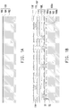
- FIG. 1A to FIG. 1D are cross-sectional views of a manufacturing process of a package structure according to a first embodiment which is not part of the invention.
- a substrate 100 is provided.
- the substrate 100 includes a first metal layer 102, a second metal layer 106 and an etching stop layer 104.
- the etching stop layer 104 is disposed between the first metal layer 102 and the second metal layer 106.
- the substrate 100 is, for example, a three-layer structure composed of Cu-Ni-Cu, or a three-layer structure composed of Cu-Al-Cu, as long as a material of the etching stop layer 104 is different to the material of the first metal layer 102 and the material of the second metal layer 106, though the invention is not limited thereto.
- the material of the first metal layer 102 is, for example, silver, nickel, copper, aluminium, gold, palladium or a combination thereof, and a thickness thereof is between 10 ⁇ m and 150 ⁇ m.
- the material of the second metal layer 106 is, for example, silver, nickel, copper, aluminium, gold, palladium or a combination thereof, and a thickness thereof is between 10 ⁇ m and 80 ⁇ m.
- the material of the etching stop layer 104 is, for example, silver, nickel, copper, aluminium, gold, palladium or a combination thereof, and a thickness thereof is between 0.5 ⁇ m and 30 ⁇ m.
- the second metal layer 106 is patterned to form a plurality of first contact pads 106a and 106b.
- the first contact pads 106a and 106 have a first surface S1 and a second surface S2 opposite to each other.
- the first contact pads 106a are not electrically connected to the subsequently formed conductive through vias 114.
- the first contact pads 106b are electrically connected to the subsequently formed conductive through vias 114.
- the circuit board 107 is formed on the first surface S1 of the first contact pads 106a and 106b.
- the circuit board 107 includes a build-up structure 108, second contact pads 116 and a solder mask layer 118.
- the build-up structure 108 includes a plurality of dielectric layers 110, a plurality of patterned circuit layers 112 and a plurality of conductive through vias 114. Each of the patterned circuit layers 112 is disposed between the adjacent dielectric layers 110.
- a method for forming the patterned circuit layers 112 is, for example, to first form a photoresist layer such as a dry film (not shown) on the first contact pads 106a and 106b or on the circuit layer.
- the photoresist layer is patterned through a photolithography process to expose one portion of the first contact pads 106a and 106b or the circuit layer. Thereafter, a electroplating process and a remove process of the photoresist layer is performed, so as to form the patterned circuit layers 112. Afterwards, the dielectric layers 110 are formed on the patterned circuit layers 112. Then, the conductive through vias 114 are formed in the dielectric layers 110, where the conductive through vias 114 are electrically connected to two adjacent patterned circuit layers 112. Although only 5-layer of the dielectric layers 110 and 5-layer of the patterned circuit layers 112 are illustrated in FIG. 1B , the present embodiment which is not part of the invention is not limited thereto.
- the number of the patterned circuit layers 112 can be added according to a build-up method, and can be adjusted according to an actual design requirement.
- a material of the dielectric layers 110 may include a dielectric material, and the dielectric material is, for example, prepreg, ajinomoto build-up film (ABF) or a combination thereof.
- a material of the patterned circuit layers 112 may include a metal material, and the metal material is, for example, silver, nickel, copper, aluminium, gold, palladium or a combination thereof.
- the patterned circuit layers 112 can be regarded as wires on the circuit board 107, which can be designed according to a required circuit layout.
- a material of the solder mask layer 118 is, for example, a dielectric material, an ABF layer or a combination thereof.
- a method for forming the solder mask layer 118 is, for example, to first form a solder mask material layer on the second contact pads 116 (not shown). Then, the solder mask material layer is patterned to expose the surface of one portion of the second contact pads 116.
- a surface treatment layer can be formed on the second contact pads 116 and between the second contact pads 116 and the solder mask layer 118 (not shown).
- a material of the surface treatment layer is, for example, organic solderability preservative (OSP), electroplating Ni/Au, electroplating Ni/Pd, electroplating Sn, electroplating Ag, electroless Au, electroless nickel electroless palladium immersion gold (ENEPIG) or a combination thereof.
- OSP organic solderability preservative
- electroplating Ni/Au electroplating Ni/Pd
- electroplating Sn electroplating Ag
- electroless Au electroless nickel electroless palladium immersion gold
- ENEPIG electroless nickel electroless palladium immersion gold
- the first metal layer 102 is patterned to form a plurality of metal pillars 102a.
- a method for forming the metal pillars 102a is, for example, to form a patterned photoresist layer on the first metal layer 102 to expose a surface of one portion of the first metal layer 102 (not shown).
- the etching stop layer 104 is taken as an etching stop layer to perform an etching process on the first metal layer 102, so as to form the metal pillars 102a.
- the etching stop layer 104 that is not covered by the metal pillars 102a is removed to expose the second surface S2 of the first contact pad 106c, so as to form the etching stop layer 104a covered by the metal pillars 102a.
- the metal pillars 102a can be electrically connected to the circuit board 107 through the etching stop layer 104a and the first contact pads 106a and 106b.
- a height of the metal pillars can be adjusted according to subsequently formed chips 124a and 125b, which is not limited by the invention.
- the chips 124a and 124b are formed on the second surface S2 of the first contact pads 106c.
- the metal pillars 102a surround the chips 124a and 124b.
- the chips 124a and 124b are electrically connected to the circuit board 107 through bumps 120 and the first contact pads 106c.
- a plurality of bumps 122 are also formed on the second contact pads 116 of the circuit board 107.
- the package structure 10 of the first embodiment can be electrically connected to other package structure through the bumps 122 to form a package-on-package (POP) structure.
- POP package-on-package
- FIG. 1D only two chips 124a and 124b are illustrated, though the invention is not limited thereto. In other embodiments, the number of the chips can be adjusted according to an actual requirement.
- the package structure 10 of the first embodiment includes the first contact pads 106a, 106b, 106c, the circuit board 107, the metal pillars 102a and the chips 124a and 124b.
- the first contact pads 106a, 106b and 106c have the first surface S1 and the second surface S2 opposite to each other.
- the circuit board 107 is disposed on the first surface S1 of the first contact pads 106a, 106b and 106c.
- the metal pillars 102a is disposed on the second surface S2 of the first contact pads 106a, 106b and 106c.
- the chips 124a and 124b are disposed on the second surface S2 of the first contact pads 106c.
- the metal pillars 102a surround the chips 124a and 124b. Since the material of the metal pillars 102a is relatively hard, and the metal pillars 102a surround the chips 124a and 124b, the structural strength of the package structure 10 of the first embodiment is strengthened. In this way, the package structure 10 of the first embodiment may resolve the warpage issue occurred in a chip bonding process, so as to improve a yield of the package structure 10.
- the method for manufacturing the package structure 10 of the first embodiment is to first form the circuit board 107 on the relatively thick substrate 100. Then, an etching process is performed on the first metal layer 102 to form the metal pillars 102a. Therefore, in view of the manufacturing process, the warpage issue of the circuit board 107 made of a relatively soft material is avoided during the manufacturing process, so as to further improve the yield of the circuit board 107.
- the same or similar components, members or layers are denoted by the similar referential numbers.
- the substrate 100 and the substrates 200, 300 and 400 are the same or similar components
- the build-up structure 108 and the build-up structures 208, 308 and 408 are the same or similar components, and details thereof are not repeated.
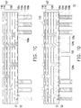
- FIG. 2A to FIG. 2D are cross-sectional views of a manufacturing process of a package structure according to a second embodiment which is not part of the invention.
- FIG. 3 is a top view of a supporting structure of FIG. 2B .
- the manufacturing process of the package structure 20 of the second embodiment which is not part of the invention is basically similar to the manufacturing process of the package structure 10 of the first embodiment, and a difference therebetween is that besides the conductive through vias 214b (similar to the conductive through vias 114 of the first embodiment), the circuit board 207 of the second embodiment further has a plurality of conductive through vias 214a disposed in the dielectric layer 210.
- the conductive through vias 214a can be disposed around the circuit board 207 (regarding the cross-sectional view of FIG. 2B , the surrounding of the circuit board 207 can be regarded to be close to two sides 226 and 228 of the circuit board 207).
- the conductive through vias 214a are aligned to each other to form a continuous structure.
- the conductive through vias 214a disposed around the circuit board 207 and having the continuous structure can be regarded as a conductive pillar, which can serve as a vertical supporting structure.
- the vertical supporting structure can be used to strengthen a structural strength of the package structure 20 of the second embodiment along a vertical direction, so as to resolve the warpage issue of the package structure to improve the yield of the package structure.
- the conductive through vias 214a can be designed according to a required circuit layout. In other words, the conductive through vias 214a and the conductive through vias 214b can be formed together without an additional process.
- the circuit board 207 of the second embodiment has a supporting structure 230.
- the supporting structure 230 can be regarded as a horizontal supporting structure, which can be designed according to a layout of the patterned circuit layer 212.
- the patterned circuit layer 212 is disposed on the dielectric layer 210.
- the patterned circuit layer 212 has a main pattern 212a and a supporting pattern 212b.
- the supporting pattern 212b is disposed around the main pattern 212a to form the horizontal supporting structure 230.
- the main pattern 212a can be regarded as wires originally designed on the circuit board 207.
- the supporting pattern 212b is disposed around the main pattern 212a to strengthen a lateral structural strength of the patterned circuit layer 212.
- the supporting pattern 212b (i.e. the supporting structure 230) can resolve the warpage issue of the package structure, so as to improve the yield of the package structure.
- each layer of the patterned circuit layer 212 may have the supporting pattern 212b disposed around the main pattern 212a to form the horizontal supporting structure 230. Therefore, the lateral structural strength of each layer of the patterned circuit layer 212 can be enhanced without an additional process.
- the supporting pattern 212b is, for example, a mesh pattern.
- the manufacturing steps thereof are the same to that of FIG. 1C and FIG. 1D , and materials, thickness and formation methods of the metal pillars 202a, the etching stop layer 204a, the bumps 220, 222 and the chips 224a and 224b are the same to that of the metal pillars 102a, the etching stop layer 104a, the bumps 120, 122 and the chips 124a and 124b of the first embodiment, so that details thereof are not repeated.
- FIG. 4A to FIG. 4D are cross-sectional views of a manufacturing process of a package structure according to a third embodiment which corresponds to the claimed invention.
- FIG. 5 is a top view of a heat dissipation structure of FIG. 4A .
- the manufacturing process of the package structure 30 of the third embodiment which corresponds to the claimed invention is basically similar to the manufacturing process of the package structure 20 of the second embodiment.
- a difference between the embodiments of FIG. 4A and FIG. 2B is that the circuit board 307 of the third embodiment further has the first heat dissipation structure 330 and a dielectric layer 332 disposed between the build-up structure 308 and the second contact pads 316.
- the first heat dissipation structure 330 is electrically connected to the vertical supporting structure 314a (i.e. the conductive through vias 314a) to form an inverted U-shape structure.
- the first heat dissipation structure 330 can be regarded as another layer of the patterned circuit layer 312 disposed between the build-up structure 308 and the second contact pads 316.
- the pattern of the first heat dissipation structure 330 includes a mesh pattern 330a, a conductive through via pattern 330b and a corner pattern 330c.
- the dielectric layer 332 is disposed on the first heat dissipation structure 330.
- the mesh pattern 330a is not only used for increasing a heat dissipation performance of the package structure 30 of the third embodiment, but also is further used for strengthening a lateral structural strength of the package structure 30 of the third embodiment.
- the conductive through via pattern 330b is used for electrically connecting the build-up structure 308 and the second contact pads 316.
- the corner pattern 330c can be electrically connected to the vertical supporting structure 314a (i.e. the conductive through via 314a) to form an inverted U-shape structure. Therefore, the corner pattern 330c not only increases a heat dissipation performance of the package structure 30 of the third embodiment, but also enhances the structural strength of the package structure 30 of the third embodiment along the vertical direction.
- a material of the first heat dissipation structure 330 may include a metal material, and the metal material is, for example, silver, nickel, copper, aluminium, gold, palladium or a combination thereof.
- a material of the dielectric layer 332 may include a dielectric material, and the dielectric material is, for example, prepreg, an ABF layer or a combination thereof.
- the manufacturing steps thereof are the same to that of FIG. 2C and FIG. 2D , and materials, thickness and formation methods of the metal pillars 302a, the etching stop layer 304a, the bumps 320, 322 and the chips 324a and 324b are the same to that of the metal pillars 202a, the etching stop layer 204a, the bumps 220, 222 and the chips 224a and 224b of the second embodiment, so that details thereof are not repeated.
- a second heat dissipation structure 334 is formed on a third surface S3 of the chips 324a and 324b.
- the second heat dissipation structure 334 may enhance the heat dissipation performance of the package structure 30 of the third embodiment to decrease a temperature of the whole package structure 30.
- a material of the second heat dissipation structure 334 is, for example, silver, nickel, copper, aluminium, gold, palladium or a combination thereof.
- FIG. 6A to FIG. 6E are cross-sectional views of a manufacturing process of a package structure according to a fourth embodiment which is not part of the invention.
- the manufacturing process of the package structure 40 of the fourth embodiment which is not part of the invention is basically similar to the manufacturing process of the package structure 10 of the first embodiment.
- Materials, thickness and formation methods of the metal pillars 402a, the etching stop layer 404a, the first contact pads 406a, 406b and 406c, the circuit board 407, the bumps 420, 422 and the chips 424a and 424b are the same to that of the metal pillars 102a, the etching stop layer 104a, the first contact pads 106a, 106b and 106c, the circuit board 107, the bumps 120, 122 and the chips 124a and 124b of the first embodiment, so that details thereof are not repeated.
- the package structure 40 of the fourth embodiment has an insulating structure 430 disposed on the second surface S2 of the first contact pads 406a, 406b and 406c.
- the insulating structure 430 does not cover the third surface S3 of the chips 424a and 424b.
- a material of the insulating structure 430 is, for example, epoxy, polyimide or a combination thereof.
- a method for forming the insulating structure 430 is, for example, to first form an insulating structure material layer on the second surface S2 of the first contact pads 406a, 406b and 406c. Then, a curing process is performed, so as to form the insulating structure 430.
- the insulating structure 430 can strengthen the structural strength of the package structure 40 of the fourth embodiment. It should be noticed that since a thickness of the insulating structure 430 is smaller than a thickness of the chips 424a and 424b, and the insulating structure 430 does not cover the third surface s3 of the chips 424a and 424b, a confliction between the chips 424a and 424b is avoided. In an embodiment, the thickness of the insulating structure 430 can be between 10 ⁇ m and 100 ⁇ m.
- the supporting structure disposed in the circuit board and the insulating structure disposed on the second surface of the first contact pads are used to enhance a strength of the package structure, so as to resolve the warpage issue of the package structure to further improve a yield of the package structure.
- the first heat dissipation structure and the second heat dissipation structure are adopted in the invention, by which not only a temperature of the package structure is decreased, but also the strength of the package structure is further enhanced.
- the manufacturing method of the invention is to first form the circuit board on the relatively thick substrate. Then, the first metal layer is etched to form a plurality of metal pillars. In this way, in view of the manufacturing process, the warpage issue of the circuit board made of a relatively soft material is avoided during the manufacturing process, so as to enhance the yield of the circuit board.
Landscapes
- Production Of Multi-Layered Print Wiring Board (AREA)
- Structures For Mounting Electric Components On Printed Circuit Boards (AREA)
- Wire Bonding (AREA)
Description
- The invention relates to a semiconductor structure and a method for manufacturing the same, and particularly relates to a three-dimensional package structure and a method for manufacturing the same.
- In recent years, in order to increase applications of printed circuit board (PCB), the PCB is fabricated into a multi-layer circuit structure according to many techniques. A method for fabricating the multi-layer circuit structure is to construct a build-up structure by using copper foils or other suitable conductive materials and prepreg (PP) or other suitable dielectric materials, and repeatedly laminate the build-up structure for stacking on a core layer, so as to form the multi-layer circuit structure, by which an internal wiring space of the multi-layer circuit structure is increased. The conductive material on the build-up structure can construct a conductive circuit according to a required circuit layout, and blind holes or through holes of the build-up structure can be filled with a conductive material for conducting each of the layers. In this way, the number of the circuit layers of the multi-layer circuit structure can be adjusted according to an actual requirement, and the multi-layer circuit structure can be manufactured according to the above method.
- However, since the prepreg or the other suitable dielectric material is relatively soft, a warpage issue of the multi-layer circuit structure is probably encountered during the manufacturing process thereof. When the above PCB is applied to a package-on-package (POP) structure, the POP structure may also have the warpage issue, by which a yield of the POP structure is decreased.
- Package structures of the prior art are known from
US 2015/041987 A1 ,US 2012/286404 A1 ,US 2015/014031 A1 ,US 2009/145635 A1 ,US 2010/175917 A1 ,CN 104 241 219 A andUS 2014/264815 A1 . - The invention is directed to a three-dimensional (3D) package structure and a method for manufacturing the same, by which a warpage issue of the 3D package structure is resolved, and a yield thereof is increased.
- The invention provides a package structure including a circuit board, a plurality of first contact pads, a plurality of metal pillars and at least one chip. The first contact pads are disposed on the circuit board. The chip is disposed on one portion of the first contact pads. The metal pillars are disposed on the other portion of the first contact pads, where the metal pillars surround the chip.
- According to the invention, the circuit board includes a build-up structure, second contact pads and a solder mask layer. The second contact pads are disposed between the build-up structure and the solder mask layer. The build-up structure includes a plurality of dielectric layers, a plurality of patterned circuit layers and a plurality of first conductive through vias. Each of the patterned circuit layers is disposed between the adjacent dielectric layers. The first conductive through vias are disposed in the dielectric layer for electrically connecting the adjacent patterned circuit layers.
- According to the invention, the package structure further includes a supporting structure disposed in the circuit board. The supporting structure includes a vertical supporting structure and a horizontal supporting structure.
- According to the invention, the vertical supporting structure has a plurality of second conductive through vias disposed in the dielectric layer and disposed around the circuit board. The second conductive through vias are aligned to each other to form a continuous structure.
- According to the invention, the package structure further includes a first heat dissipation structure disposed between the build-up structure and the second contact pads. The first heat dissipation structure is electrically connected to the vertical supporting structure to form an inverted U-shape structure.
- According to an embodiment which is not part of the invention, the patterned circuit layer has a main pattern and a supporting pattern. The supporting pattern is disposed around the main pattern to form the horizontal supporting structure. The supporting pattern is a mesh pattern.
- According to an advantageous embodiment of the invention, the package structure further includes a second heat dissipation structure disposed on the chip.
- According to an advantageous embodiment of the invention, a material of the second heat dissipation structure includes silver, nickel, copper, aluminium, gold, palladium or a combination thereof.
- According to an embodiment which is not part of the invention, the package structure further includes an insulating structure disposed on the first contact pads. The insulating structure does not cover a surface of the chip.
- According to an embodiment which is not part of the invention, a material of the insulating structure includes epoxy, polyimide or a combination thereof.
- According to an advantageous embodiment of the invention, the package structure further includes a plurality of bumps and a plurality of etching stop layers. The bumps are disposed between the first contact pads and the chip. The etching stop layers are disposed between the first contact pads and the metal pillars.
- The invention provides a method for manufacturing a package structure, which includes following steps. A substrate is provided. The substrate includes a first metal layer, a second metal layer and an etching stop layer. The etching stop layer is disposed between the first metal layer and the second metal layer. The second metal layer is patterned to form a plurality of first contact pads. A circuit board is formed on a first surface of the first contact pads. The first metal layer is patterned to form a plurality of metal pillars. The etching stop layer that is not covered by the metal pillars is removed to expose a second surface of the first contact pads. The metal pillars are electrically connected to the circuit board through the first contact pads and the etching stop layer covered by the metal pillars. At least one chip is formed on the second surface of the first contact pads, where the metal pillars surround the chip.
- According to the invention, the circuit board includes a build-up structure, second contact pads and a solder mask layer. The second contact pads are disposed between the build-up structure and the solder mask layer. The build-up structure includes a plurality of dielectric layers, a plurality of patterned circuit layers and a plurality of first conductive through vias. Each of the patterned circuit layers is disposed between the adjacent dielectric layers. The first conductive through vias are disposed in the dielectric layer for electrically connecting the adjacent patterned circuit layers.
- According to the invention, the method for manufacturing the package structure further includes forming a supporting structure in the circuit board. The supporting structure includes a vertical supporting structure and a horizontal supporting structure.
- According to the invention, the vertical supporting structure has a plurality of second conductive through vias disposed in the dielectric layer and disposed around the circuit board. The second conductive through vias are aligned to each other to form a continuous structure.
- According to the invention, the method for manufacturing the package structure further includes forming a first heat dissipation structure between the build-up structure and the second contact pads. The first heat dissipation structure is electrically connected to the vertical supporting structure to form an inverted U-shape structure.
- According to an embodiment which is not part of the invention, the patterned circuit layer has a main pattern and a supporting pattern. The supporting pattern is disposed around the main pattern to form the horizontal supporting structure. The supporting pattern is a mesh pattern.
- According to an advantageous embodiment of the invention, the method for manufacturing the package structure further includes forming a second heat dissipation structure on a third surface of the chip.
- According to an embodiment which is not part of the invention, the method for manufacturing the package structure further includes forming an insulating structure on the second surface of the first contact pads. The insulating structure does not cover the third surface of the chip.
- According to an advantageous embodiment of the invention, the method for manufacturing the package structure further includes forming a plurality of bumps between the first contact pads and the chip.
- According to the above descriptions, the supporting structure disposed in the circuit board and the insulating structure disposed on the second surface of the first contact pads are used to enhance the strength of the package structure, so as to resolve the warpage issue of the package structure to further improve a yield of the package structure. Moreover, the first heat dissipation structure and the second heat dissipation structure are adopted in the invention, by which not only a temperature of the package structure is decreased, but also the strength of the package structure is further enhanced.
- To make the aforementioned and other features and advantages of the invention more comprehensible, several embodiments, which are part or not of the present invention, accompanied with drawings are described in detail as follows.
-
-
FIG. 1A to FIG. 1D are cross-sectional views of a manufacturing process of a package structure according to a first embodiment which is not part of the invention. -
FIG. 2A to FIG. 2D are cross-sectional views of a manufacturing process of a package structure according to a second embodiment which is not part of the invention. -
FIG. 3 is a top view of a supporting structure ofFIG. 2B . -
FIG. 4A to FIG. 4D are cross-sectional views of a manufacturing process of a package structure according to a third embodiment which corresponds to the claimed invention. -
FIG. 5 is a top view of a heat dissipation structure ofFIG. 4A . -
FIG. 6A to FIG. 6E are cross-sectional views of a manufacturing process of a package structure according to a fourth embodiment which is not part of the invention. -
FIG. 1A to FIG. 1D are cross-sectional views of a manufacturing process of a package structure according to a first embodiment which is not part of the invention. - Referring to
FIG. 1A , asubstrate 100 is provided. Thesubstrate 100 includes afirst metal layer 102, asecond metal layer 106 and anetching stop layer 104. Theetching stop layer 104 is disposed between thefirst metal layer 102 and thesecond metal layer 106. In the present embodiment, thesubstrate 100 is, for example, a three-layer structure composed of Cu-Ni-Cu, or a three-layer structure composed of Cu-Al-Cu, as long as a material of theetching stop layer 104 is different to the material of thefirst metal layer 102 and the material of thesecond metal layer 106, though the invention is not limited thereto. In another embodiment, the material of thefirst metal layer 102 is, for example, silver, nickel, copper, aluminium, gold, palladium or a combination thereof, and a thickness thereof is between 10 µm and 150 µm. The material of thesecond metal layer 106 is, for example, silver, nickel, copper, aluminium, gold, palladium or a combination thereof, and a thickness thereof is between 10 µm and 80 µm. The material of theetching stop layer 104 is, for example, silver, nickel, copper, aluminium, gold, palladium or a combination thereof, and a thickness thereof is between 0.5 µm and 30 µm. - Then, referring to
FIG. 1A and FIG. 1B , thesecond metal layer 106 is patterned to form a plurality offirst contact pads first contact pads first contact pads 106a are not electrically connected to the subsequently formed conductive throughvias 114. Thefirst contact pads 106b are electrically connected to the subsequently formed conductive throughvias 114. - Thereafter, a
circuit board 107 is formed on the first surface S1 of thefirst contact pads circuit board 107 includes a build-upstructure 108,second contact pads 116 and asolder mask layer 118. In detail, the build-upstructure 108 includes a plurality ofdielectric layers 110, a plurality of patterned circuit layers 112 and a plurality of conductive throughvias 114. Each of the patterned circuit layers 112 is disposed between the adjacent dielectric layers 110. A method for forming the patterned circuit layers 112 is, for example, to first form a photoresist layer such as a dry film (not shown) on thefirst contact pads first contact pads dielectric layers 110 are formed on the patterned circuit layers 112. Then, the conductive throughvias 114 are formed in thedielectric layers 110, where the conductive throughvias 114 are electrically connected to two adjacent patterned circuit layers 112. Although only 5-layer of thedielectric layers 110 and 5-layer of the patterned circuit layers 112 are illustrated inFIG. 1B , the present embodiment which is not part of the invention is not limited thereto. Basically, the number of the patterned circuit layers 112 can be added according to a build-up method, and can be adjusted according to an actual design requirement. A material of thedielectric layers 110 may include a dielectric material, and the dielectric material is, for example, prepreg, ajinomoto build-up film (ABF) or a combination thereof. A material of the patterned circuit layers 112 may include a metal material, and the metal material is, for example, silver, nickel, copper, aluminium, gold, palladium or a combination thereof. In the present embodiment, the patterned circuit layers 112 can be regarded as wires on thecircuit board 107, which can be designed according to a required circuit layout. - Then, the
second contact pads 116 and thesolder mask layer 118 are formed on the build-upstructure 108. The material of thesecond contact pads 116 and the method for forming the same are similar to that of the aforementioned patternedcircuit layer 112, which are not repeated. In the present embodiment, a material of thesolder mask layer 118 is, for example, a dielectric material, an ABF layer or a combination thereof. A method for forming thesolder mask layer 118 is, for example, to first form a solder mask material layer on the second contact pads 116 (not shown). Then, the solder mask material layer is patterned to expose the surface of one portion of thesecond contact pads 116. Moreover, a surface treatment layer can be formed on thesecond contact pads 116 and between thesecond contact pads 116 and the solder mask layer 118 (not shown). A material of the surface treatment layer is, for example, organic solderability preservative (OSP), electroplating Ni/Au, electroplating Ni/Pd, electroplating Sn, electroplating Ag, electroless Au, electroless nickel electroless palladium immersion gold (ENEPIG) or a combination thereof. - Referring to
FIG. 1C , thefirst metal layer 102 is patterned to form a plurality ofmetal pillars 102a. In detail, a method for forming themetal pillars 102a is, for example, to form a patterned photoresist layer on thefirst metal layer 102 to expose a surface of one portion of the first metal layer 102 (not shown). Then, theetching stop layer 104 is taken as an etching stop layer to perform an etching process on thefirst metal layer 102, so as to form themetal pillars 102a. Thereafter, theetching stop layer 104 that is not covered by themetal pillars 102a is removed to expose the second surface S2 of thefirst contact pad 106c, so as to form theetching stop layer 104a covered by themetal pillars 102a. Themetal pillars 102a can be electrically connected to thecircuit board 107 through theetching stop layer 104a and thefirst contact pads chips 124a and 125b, which is not limited by the invention. - Referring to
FIG. 1D , thechips first contact pads 106c. Themetal pillars 102a surround thechips chips circuit board 107 throughbumps 120 and thefirst contact pads 106c. On the other hand, a plurality ofbumps 122 are also formed on thesecond contact pads 116 of thecircuit board 107. Thepackage structure 10 of the first embodiment can be electrically connected to other package structure through thebumps 122 to form a package-on-package (POP) structure. InFIG. 1D , only twochips - Referring to
FIG. 1D , thepackage structure 10 of the first embodiment includes thefirst contact pads circuit board 107, themetal pillars 102a and thechips first contact pads circuit board 107 is disposed on the first surface S1 of thefirst contact pads metal pillars 102a is disposed on the second surface S2 of thefirst contact pads chips first contact pads 106c. Themetal pillars 102a surround thechips metal pillars 102a is relatively hard, and themetal pillars 102a surround thechips package structure 10 of the first embodiment is strengthened. In this way, thepackage structure 10 of the first embodiment may resolve the warpage issue occurred in a chip bonding process, so as to improve a yield of thepackage structure 10. - Moreover, the method for manufacturing the
package structure 10 of the first embodiment is to first form thecircuit board 107 on the relativelythick substrate 100. Then, an etching process is performed on thefirst metal layer 102 to form themetal pillars 102a. Therefore, in view of the manufacturing process, the warpage issue of thecircuit board 107 made of a relatively soft material is avoided during the manufacturing process, so as to further improve the yield of thecircuit board 107. - In the following embodiment which is not part of the invention, the same or similar components, members or layers are denoted by the similar referential numbers. For example, the
substrate 100 and thesubstrates structure 108 and the build-upstructures -
FIG. 2A to FIG. 2D are cross-sectional views of a manufacturing process of a package structure according to a second embodiment which is not part of the invention.FIG. 3 is a top view of a supporting structure ofFIG. 2B . - Referring to
FIG. 2A to FIG. 2C , the manufacturing process of the package structure 20 of the second embodiment which is not part of the invention is basically similar to the manufacturing process of thepackage structure 10 of the first embodiment, and a difference therebetween is that besides the conductive throughvias 214b (similar to the conductive throughvias 114 of the first embodiment), thecircuit board 207 of the second embodiment further has a plurality of conductive throughvias 214a disposed in thedielectric layer 210. The conductive through vias 214a can be disposed around the circuit board 207 (regarding the cross-sectional view ofFIG. 2B , the surrounding of thecircuit board 207 can be regarded to be close to twosides vias 214a are aligned to each other to form a continuous structure. In the present embodiment, the conductive through vias 214a disposed around thecircuit board 207 and having the continuous structure can be regarded as a conductive pillar, which can serve as a vertical supporting structure. The vertical supporting structure can be used to strengthen a structural strength of the package structure 20 of the second embodiment along a vertical direction, so as to resolve the warpage issue of the package structure to improve the yield of the package structure. In the present embodiment, the conductive through vias 214a can be designed according to a required circuit layout. In other words, the conductive throughvias 214a and the conductive throughvias 214b can be formed together without an additional process. - Moreover, the
circuit board 207 of the second embodiment has a supportingstructure 230. Referring toFIG. 2B andFIG. 3 , the supportingstructure 230 can be regarded as a horizontal supporting structure, which can be designed according to a layout of the patternedcircuit layer 212. In detail, the patternedcircuit layer 212 is disposed on thedielectric layer 210. The patternedcircuit layer 212 has amain pattern 212a and a supportingpattern 212b. The supportingpattern 212b is disposed around themain pattern 212a to form the horizontal supportingstructure 230. Themain pattern 212a can be regarded as wires originally designed on thecircuit board 207. The supportingpattern 212b is disposed around themain pattern 212a to strengthen a lateral structural strength of the patternedcircuit layer 212. Therefore, the supportingpattern 212b (i.e. the supporting structure 230) can resolve the warpage issue of the package structure, so as to improve the yield of the package structure. Generally, each layer of the patternedcircuit layer 212 may have the supportingpattern 212b disposed around themain pattern 212a to form the horizontal supportingstructure 230. Therefore, the lateral structural strength of each layer of the patternedcircuit layer 212 can be enhanced without an additional process. In the present embodiment, the supportingpattern 212b is, for example, a mesh pattern. - Referring to
FIG. 2C and FIG. 2D , the manufacturing steps thereof are the same to that ofFIG. 1C and FIG. 1D , and materials, thickness and formation methods of themetal pillars 202a, theetching stop layer 204a, thebumps chips metal pillars 102a, theetching stop layer 104a, thebumps chips -
FIG. 4A to FIG. 4D are cross-sectional views of a manufacturing process of a package structure according to a third embodiment which corresponds to the claimed invention.FIG. 5 is a top view of a heat dissipation structure ofFIG. 4A . - The manufacturing process of the
package structure 30 of the third embodiment which corresponds to the claimed invention is basically similar to the manufacturing process of the package structure 20 of the second embodiment. Referring toFIG. 4A ,FIG. 2B andFIG. 5 , a difference between the embodiments ofFIG. 4A andFIG. 2B is that thecircuit board 307 of the third embodiment further has the firstheat dissipation structure 330 and adielectric layer 332 disposed between the build-upstructure 308 and thesecond contact pads 316. As shown inFIG. 4A , the firstheat dissipation structure 330 is electrically connected to the vertical supportingstructure 314a (i.e. the conductive through vias 314a) to form an inverted U-shape structure. In detail, the firstheat dissipation structure 330 can be regarded as another layer of the patternedcircuit layer 312 disposed between the build-upstructure 308 and thesecond contact pads 316. As shown inFIG. 5 , the pattern of the firstheat dissipation structure 330 includes a mesh pattern 330a, a conductive through via pattern 330b and a corner pattern 330c. Thedielectric layer 332 is disposed on the firstheat dissipation structure 330. The mesh pattern 330a is not only used for increasing a heat dissipation performance of thepackage structure 30 of the third embodiment, but also is further used for strengthening a lateral structural strength of thepackage structure 30 of the third embodiment. The conductive through via pattern 330b is used for electrically connecting the build-upstructure 308 and thesecond contact pads 316. The corner pattern 330c can be electrically connected to the vertical supportingstructure 314a (i.e. the conductive through via 314a) to form an inverted U-shape structure. Therefore, the corner pattern 330c not only increases a heat dissipation performance of thepackage structure 30 of the third embodiment, but also enhances the structural strength of thepackage structure 30 of the third embodiment along the vertical direction. In the present embodiment, a material of the firstheat dissipation structure 330 may include a metal material, and the metal material is, for example, silver, nickel, copper, aluminium, gold, palladium or a combination thereof. A material of thedielectric layer 332 may include a dielectric material, and the dielectric material is, for example, prepreg, an ABF layer or a combination thereof. - Referring to
FIG. 4B andFIG. 4C , the manufacturing steps thereof are the same to that ofFIG. 2C and FIG. 2D , and materials, thickness and formation methods of themetal pillars 302a, theetching stop layer 304a, thebumps chips metal pillars 202a, theetching stop layer 204a, thebumps chips - Referring to
FIG. 4D , a secondheat dissipation structure 334 is formed on a third surface S3 of thechips heat dissipation structure 334 may enhance the heat dissipation performance of thepackage structure 30 of the third embodiment to decrease a temperature of thewhole package structure 30. In the present embodiment, a material of the secondheat dissipation structure 334 is, for example, silver, nickel, copper, aluminium, gold, palladium or a combination thereof. -
FIG. 6A to FIG. 6E are cross-sectional views of a manufacturing process of a package structure according to a fourth embodiment which is not part of the invention. - Referring to
FIG. 6A to FIG. 6D , the manufacturing process of thepackage structure 40 of the fourth embodiment which is not part of the invention is basically similar to the manufacturing process of thepackage structure 10 of the first embodiment. Materials, thickness and formation methods of themetal pillars 402a, theetching stop layer 404a, thefirst contact pads circuit board 407, thebumps chips metal pillars 102a, theetching stop layer 104a, thefirst contact pads circuit board 107, thebumps chips - Referring to
FIG. 6E , different to thepackage structure 10 of the first embodiment, thepackage structure 40 of the fourth embodiment has an insulatingstructure 430 disposed on the second surface S2 of thefirst contact pads structure 430 does not cover the third surface S3 of thechips structure 430 is, for example, epoxy, polyimide or a combination thereof. A method for forming the insulatingstructure 430 is, for example, to first form an insulating structure material layer on the second surface S2 of thefirst contact pads structure 430. Since the material of the insulatingstructure 430 is relatively hard, the insulatingstructure 430 can strengthen the structural strength of thepackage structure 40 of the fourth embodiment. It should be noticed that since a thickness of the insulatingstructure 430 is smaller than a thickness of thechips structure 430 does not cover the third surface s3 of thechips chips structure 430 can be between 10 µm and 100 µm. - In summary, the supporting structure disposed in the circuit board and the insulating structure disposed on the second surface of the first contact pads are used to enhance a strength of the package structure, so as to resolve the warpage issue of the package structure to further improve a yield of the package structure. Also, the first heat dissipation structure and the second heat dissipation structure are adopted in the invention, by which not only a temperature of the package structure is decreased, but also the strength of the package structure is further enhanced.
- Moreover, the manufacturing method of the invention is to first form the circuit board on the relatively thick substrate. Then, the first metal layer is etched to form a plurality of metal pillars. In this way, in view of the manufacturing process, the warpage issue of the circuit board made of a relatively soft material is avoided during the manufacturing process, so as to enhance the yield of the circuit board.
Claims (5)
- A package structure (30), comprising:a circuit board (307), wherein the circuit board (307) comprises a build-up structure (308), second contact pads (316) and a solder mask layer (318), the second contact pads (316) being disposed between the build-up structure (308) and the solder mask layer (318), and wherein the build-up structure (308) comprises:a plurality of dielectric layers (310);a plurality of patterned circuit layers (312), each of the patterned circuit layers (312) being disposed between the adjacent dielectric layers (310); anda plurality of first conductive through vias (314a), disposed in the dielectric layers (310), and electrically connecting the adjacent patterned circuit layers (312);a supporting structure (314a, 330), disposed in the circuit board (307), wherein the supporting structure (314a, 330) comprises a vertical supporting structure (314a) and a horizontal supporting structure (330), wherein the vertical supporting structure (314a) has a plurality of second conductive through vias (314a) disposed in the dielectric layers (310) and disposed at the outer circumference of the circuit board (307), the second conductive through vias (314a) being aligned to each other to form a continuous structure;a first heat dissipation structure (330), disposed in the circuit board (307) and between the build-up structure (308) and the second contact pads (316), wherein the first heat dissipation structure (330) is electrically connected to the vertical supporting structure (314a) to form an inverted U-shape structure;a plurality of first contact pads (306a-306c), disposed on the circuit board (307);at least one chip (324a, 324b), disposed on one portion of the first contact pads (306c); anda plurality of metal pillars (302a), disposed on the other portion of the first contact pads (306a-306b), wherein the metal pillars (302a) surround the at least one chip (324a, 324b).
- The package structure (30) as claimed in claim 1, further comprising a second heat dissipation structure (334) disposed on the chip (324a, 324b).
- The package structure (30) as claimed in claim 1, further comprising:a plurality of bumps (320), disposed between the first contact pads (306c) and the chip (324a, 324b); anda plurality of metal layers (304a), disposed between the first contact pads (306a-306b) and the metal pillars (302a).
- A method for manufacturing a package structure (30), comprising:providing a substrate (300) comprising a first metal layer (302), a second metal layer (306) and an etching stop layer (304), wherein the etching stop layer (304) is disposed between the first metal layer (302) and the second metal layer (306);patterning the second metal layer (306) to form a plurality of first contact pads (306a-306c);forming a circuit board (307) on a first surface (S1) of the first contact pads (306a-306c), wherein the circuit board (307) comprises a build-up structure (308), second contact pads (316) and a solder mask layer (318), the second contact pads (316) being disposed between the build-up structure (308) and the solder mask layer (318), wherein the build-up structure (308) comprises:a plurality of dielectric layers (310);a plurality of patterned circuit layers (312), each of the patterned circuit layers (312) being disposed between the adjacent dielectric layers (310); anda plurality of first conductive through vias (314a) disposed in the dielectric layers (310), and electrically connecting the adjacent patterned circuit layers (312);patterning the first metal layer (302) to form a plurality of metal pillars (302a);removing the etching stop layer (304) that is not covered by the metal pillars (302a) to expose a second surface (S2) of the first contact pads (306a-306c), wherein the metal pillars (302a) are electrically connected to the circuit board (307) through the first contact pads (306a-306b) and the etching stop layer (304a) covered by the metal pillars (302a);forming at least one chip (324a, 324b) on the second surface (S2) of the first contact pads (306c), wherein the at least one chip (324a, 324b) is surrounded by the metal pillars (302a);forming a supporting structure (314a, 330) in the circuit board (307), wherein the supporting structure (314a, 330) comprises a vertical supporting structure (314a) and a horizontal supporting structure (330) and wherein the vertical supporting structure (314a) has a plurality of second conductive through vias (314a) disposed in the dielectric layers (310) and disposed around the circuit board (307), the second conductive through vias (314a) are aligned to each other to form a continuous structure; andforming a first heat dissipation structure (330) in the circuit board (307) and between the build-up structure (308) and the second contact pads (316), wherein the first heat dissipation structure (330) is electrically connected to the vertical supporting structure (314a) to form an inverted U-shape structure.
- The method for manufacturing the package structure (30) as claimed in claim 4, further comprising:
forming a second heat dissipation structure (334) on a third surface (S3) of the at least one chip (324a, 324b).
Applications Claiming Priority (1)
| Application Number | Priority Date | Filing Date | Title |
|---|---|---|---|
| TW104116526A TWI595810B (en) | 2015-05-22 | 2015-05-22 | Package structure and manufacturing method thereof |
Publications (3)
| Publication Number | Publication Date |
|---|---|
| EP3104408A2 EP3104408A2 (en) | 2016-12-14 |
| EP3104408A3 EP3104408A3 (en) | 2017-03-29 |
| EP3104408B1 true EP3104408B1 (en) | 2019-04-17 |
Family
ID=54014624
Family Applications (1)
| Application Number | Title | Priority Date | Filing Date |
|---|---|---|---|
| EP15183101.3A Active EP3104408B1 (en) | 2015-05-22 | 2015-08-31 | Package structure and method for manufacturing the same |
Country Status (3)
| Country | Link |
|---|---|
| US (1) | US9559045B2 (en) |
| EP (1) | EP3104408B1 (en) |
| TW (1) | TWI595810B (en) |
Families Citing this family (9)
| Publication number | Priority date | Publication date | Assignee | Title |
|---|---|---|---|---|
| JP6276721B2 (en) * | 2015-02-06 | 2018-02-07 | 日立オートモティブシステムズ株式会社 | Power module |
| MY172923A (en) * | 2016-03-31 | 2019-12-13 | Twisden Ltd | Integrated circuit package having pin up interconnect |
| MY181637A (en) | 2016-03-31 | 2020-12-30 | Qdos Flexcircuits Sdn Bhd | Single layer integrated circuit package |
| CN208938956U (en) * | 2017-11-07 | 2019-06-04 | 台湾东电化股份有限公司 | Substrate structure |
| US10368448B2 (en) | 2017-11-11 | 2019-07-30 | At&S Austria Technologie & Systemtechnik Aktiengesellschaft | Method of manufacturing a component carrier |
| TWI753468B (en) * | 2020-06-24 | 2022-01-21 | 欣興電子股份有限公司 | Substrate structure with heat dissipation structure and manufacturing method thereof |
| US11257742B2 (en) * | 2020-07-02 | 2022-02-22 | Advanced Semiconductor Engineering, Inc. | Wiring structure and method for manufacturing the same |
| TWI759095B (en) * | 2021-02-04 | 2022-03-21 | 欣興電子股份有限公司 | Package structure and manufacturing method thereof |
| US12438007B2 (en) | 2021-11-12 | 2025-10-07 | Taiwan Semiconductor Manufacturing Co., Ltd. | Staggered metal mesh on backside of device die and method forming same |
Family Cites Families (15)
| Publication number | Priority date | Publication date | Assignee | Title |
|---|---|---|---|---|
| TW508987B (en) * | 2001-07-27 | 2002-11-01 | Phoenix Prec Technology Corp | Method of forming electroplated solder on organic printed circuit board |
| JP2003209366A (en) * | 2002-01-15 | 2003-07-25 | Sony Corp | Flexible multilayer wiring board and method of manufacturing the same |
| US20040084206A1 (en) * | 2002-11-06 | 2004-05-06 | I-Chung Tung | Fine pad pitch organic circuit board for flip chip joints and board to board solder joints and method |
| TWI303105B (en) * | 2006-01-11 | 2008-11-11 | Advanced Semiconductor Eng | Wafer level package for image sensor components and its fabricating method |
| TWI353047B (en) * | 2006-12-28 | 2011-11-21 | Siliconware Precision Industries Co Ltd | Heat-dissipating-type semiconductor package |
| JP4993739B2 (en) * | 2007-12-06 | 2012-08-08 | 新光電気工業株式会社 | WIRING BOARD, MANUFACTURING METHOD THEREOF, AND ELECTRONIC COMPONENT DEVICE |
| JP5339928B2 (en) * | 2009-01-15 | 2013-11-13 | 新光電気工業株式会社 | Wiring board and manufacturing method thereof |
| JP5147779B2 (en) * | 2009-04-16 | 2013-02-20 | 新光電気工業株式会社 | Wiring board manufacturing method and semiconductor package manufacturing method |
| US8039304B2 (en) * | 2009-08-12 | 2011-10-18 | Stats Chippac, Ltd. | Semiconductor device and method of dual-molding die formed on opposite sides of build-up interconnect structures |
| US8169065B2 (en) * | 2009-12-22 | 2012-05-01 | Epic Technologies, Inc. | Stackable circuit structures and methods of fabrication thereof |
| US8901732B2 (en) * | 2013-03-12 | 2014-12-02 | Taiwan Semiconductor Manufacturing Company, Ltd. | Semiconductor device package and method |
| US9406641B2 (en) * | 2013-07-10 | 2016-08-02 | Kinsus Interconnect Technology Corp. | Compound carrier board structure of flip-chip chip-scale package and manufacturing method thereof |
| US9252076B2 (en) * | 2013-08-07 | 2016-02-02 | Taiwan Semiconductor Manufacturing Company, Ltd. | 3D packages and methods for forming the same |
| US9165877B2 (en) * | 2013-10-04 | 2015-10-20 | Mediatek Inc. | Fan-out semiconductor package with copper pillar bumps |
| CN104241219B (en) * | 2014-08-26 | 2019-06-21 | 日月光半导体制造股份有限公司 | Element embedded packaging structure and manufacturing method thereof |
-
2015
- 2015-05-22 TW TW104116526A patent/TWI595810B/en active
- 2015-07-15 US US14/799,593 patent/US9559045B2/en active Active
- 2015-08-31 EP EP15183101.3A patent/EP3104408B1/en active Active
Non-Patent Citations (1)
| Title |
|---|
| None * |
Also Published As
| Publication number | Publication date |
|---|---|
| EP3104408A3 (en) | 2017-03-29 |
| TW201642714A (en) | 2016-12-01 |
| TWI595810B (en) | 2017-08-11 |
| US20160343645A1 (en) | 2016-11-24 |
| US9559045B2 (en) | 2017-01-31 |
| EP3104408A2 (en) | 2016-12-14 |
Similar Documents
| Publication | Publication Date | Title |
|---|---|---|
| US9559045B2 (en) | Package structure and method for manufacturing the same | |
| CN106165554B (en) | Printed circuit board, package substrate and manufacturing method thereof | |
| CN104332417B (en) | Manufacturing method of embedded semiconductor packaging part | |
| TWI508196B (en) | Method for manufacturing recessed substrate with built-in reinforcing layer | |
| KR100395862B1 (en) | Flip chip type semiconductor device and method for manufacturing the same | |
| US8941016B2 (en) | Laminated wiring board and manufacturing method for same | |
| TWI446464B (en) | Package structure and manufacturing method thereof | |
| JP5945564B2 (en) | Package carrier and manufacturing method thereof | |
| CN115020243B (en) | Intermediate substrate and method for making the same | |
| KR101883046B1 (en) | Coil Electronic Component | |
| KR20160002069A (en) | Pcb, package substrate and a manufacturing method thereof | |
| US20100289132A1 (en) | Substrate having embedded single patterned metal layer, and package applied with the same, and methods of manufacturing of the substrate and package | |
| TWI517269B (en) | Cascaded package structure and its preparation method | |
| JP2014187350A (en) | Component built-in board, method of manufacturing the same, and mounting body | |
| US8334590B1 (en) | Semiconductor device having insulating and interconnection layers | |
| CN106298707B (en) | Package structure and method of making the same | |
| JP6505521B2 (en) | WIRING BOARD, SEMICONDUCTOR DEVICE, AND WIRING BOARD MANUFACTURING METHOD | |
| CN102711390A (en) | Circuit board manufacturing method | |
| TWI566330B (en) | Electronic packaging structure | |
| CN104576402B (en) | Package carrier and method for manufacturing the same | |
| JP6062884B2 (en) | Component-embedded substrate, manufacturing method thereof, and mounting body | |
| KR20140079204A (en) | Semiconductor package substrate, semiconductor package and the method for fabricating same of | |
| KR101553474B1 (en) | Method of manufacturing embedded type printed circuit board and stack package including the embedded type printed circuit board | |
| JP6105517B2 (en) | Wiring board | |
| CN112151433B (en) | Substrate structure, packaging structure and manufacturing method thereof |
Legal Events
| Date | Code | Title | Description |
|---|---|---|---|
| PUAI | Public reference made under article 153(3) epc to a published international application that has entered the european phase |
Free format text: ORIGINAL CODE: 0009012 |
|
| STAA | Information on the status of an ep patent application or granted ep patent |
Free format text: STATUS: REQUEST FOR EXAMINATION WAS MADE |
|
| 17P | Request for examination filed |
Effective date: 20150831 |
|
| AK | Designated contracting states |
Kind code of ref document: A2 Designated state(s): AL AT BE BG CH CY CZ DE DK EE ES FI FR GB GR HR HU IE IS IT LI LT LU LV MC MK MT NL NO PL PT RO RS SE SI SK SM TR |
|
| AX | Request for extension of the european patent |
Extension state: BA ME |
|
| PUAL | Search report despatched |
Free format text: ORIGINAL CODE: 0009013 |
|
| AK | Designated contracting states |
Kind code of ref document: A3 Designated state(s): AL AT BE BG CH CY CZ DE DK EE ES FI FR GB GR HR HU IE IS IT LI LT LU LV MC MK MT NL NO PL PT RO RS SE SI SK SM TR |
|
| AX | Request for extension of the european patent |
Extension state: BA ME |
|
| RIC1 | Information provided on ipc code assigned before grant |
Ipc: H01L 25/065 20060101ALI20170223BHEP Ipc: H01L 23/373 20060101ALI20170223BHEP Ipc: H01L 23/36 20060101ALI20170223BHEP Ipc: H01L 23/16 20060101ALI20170223BHEP Ipc: H01L 23/538 20060101ALI20170223BHEP Ipc: H01L 23/00 20060101ALI20170223BHEP Ipc: H01L 23/498 20060101AFI20170223BHEP Ipc: H01L 25/10 20060101ALI20170223BHEP Ipc: H01L 21/48 20060101ALI20170223BHEP |
|
| RBV | Designated contracting states (corrected) |
Designated state(s): AL AT BE BG CH CY CZ DE DK EE ES FI FR GB GR HR HU IE IS IT LI LT LU LV MC MK MT NL NO PL PT RO RS SE SI SK SM TR |
|
| GRAP | Despatch of communication of intention to grant a patent |
Free format text: ORIGINAL CODE: EPIDOSNIGR1 |
|
| STAA | Information on the status of an ep patent application or granted ep patent |
Free format text: STATUS: GRANT OF PATENT IS INTENDED |
|
| INTG | Intention to grant announced |
Effective date: 20181105 |
|
| GRAS | Grant fee paid |
Free format text: ORIGINAL CODE: EPIDOSNIGR3 |
|
| GRAA | (expected) grant |
Free format text: ORIGINAL CODE: 0009210 |
|
| STAA | Information on the status of an ep patent application or granted ep patent |
Free format text: STATUS: THE PATENT HAS BEEN GRANTED |
|
| AK | Designated contracting states |
Kind code of ref document: B1 Designated state(s): AL AT BE BG CH CY CZ DE DK EE ES FI FR GB GR HR HU IE IS IT LI LT LU LV MC MK MT NL NO PL PT RO RS SE SI SK SM TR |
|
| REG | Reference to a national code |
Ref country code: GB Ref legal event code: FG4D |
|
| REG | Reference to a national code |
Ref country code: CH Ref legal event code: EP |
|
| REG | Reference to a national code |
Ref country code: DE Ref legal event code: R096 Ref document number: 602015028359 Country of ref document: DE |
|
| REG | Reference to a national code |
Ref country code: AT Ref legal event code: REF Ref document number: 1122500 Country of ref document: AT Kind code of ref document: T Effective date: 20190515 Ref country code: IE Ref legal event code: FG4D |
|
| REG | Reference to a national code |
Ref country code: NL Ref legal event code: MP Effective date: 20190417 |
|
| REG | Reference to a national code |
Ref country code: LT Ref legal event code: MG4D |
|
| PG25 | Lapsed in a contracting state [announced via postgrant information from national office to epo] |
Ref country code: NL Free format text: LAPSE BECAUSE OF FAILURE TO SUBMIT A TRANSLATION OF THE DESCRIPTION OR TO PAY THE FEE WITHIN THE PRESCRIBED TIME-LIMIT Effective date: 20190417 |
|
| PG25 | Lapsed in a contracting state [announced via postgrant information from national office to epo] |
Ref country code: NO Free format text: LAPSE BECAUSE OF FAILURE TO SUBMIT A TRANSLATION OF THE DESCRIPTION OR TO PAY THE FEE WITHIN THE PRESCRIBED TIME-LIMIT Effective date: 20190717 Ref country code: HR Free format text: LAPSE BECAUSE OF FAILURE TO SUBMIT A TRANSLATION OF THE DESCRIPTION OR TO PAY THE FEE WITHIN THE PRESCRIBED TIME-LIMIT Effective date: 20190417 Ref country code: SE Free format text: LAPSE BECAUSE OF FAILURE TO SUBMIT A TRANSLATION OF THE DESCRIPTION OR TO PAY THE FEE WITHIN THE PRESCRIBED TIME-LIMIT Effective date: 20190417 Ref country code: FI Free format text: LAPSE BECAUSE OF FAILURE TO SUBMIT A TRANSLATION OF THE DESCRIPTION OR TO PAY THE FEE WITHIN THE PRESCRIBED TIME-LIMIT Effective date: 20190417 Ref country code: PT Free format text: LAPSE BECAUSE OF FAILURE TO SUBMIT A TRANSLATION OF THE DESCRIPTION OR TO PAY THE FEE WITHIN THE PRESCRIBED TIME-LIMIT Effective date: 20190817 Ref country code: ES Free format text: LAPSE BECAUSE OF FAILURE TO SUBMIT A TRANSLATION OF THE DESCRIPTION OR TO PAY THE FEE WITHIN THE PRESCRIBED TIME-LIMIT Effective date: 20190417 Ref country code: AL Free format text: LAPSE BECAUSE OF FAILURE TO SUBMIT A TRANSLATION OF THE DESCRIPTION OR TO PAY THE FEE WITHIN THE PRESCRIBED TIME-LIMIT Effective date: 20190417 Ref country code: LT Free format text: LAPSE BECAUSE OF FAILURE TO SUBMIT A TRANSLATION OF THE DESCRIPTION OR TO PAY THE FEE WITHIN THE PRESCRIBED TIME-LIMIT Effective date: 20190417 |
|
| PG25 | Lapsed in a contracting state [announced via postgrant information from national office to epo] |
Ref country code: BG Free format text: LAPSE BECAUSE OF FAILURE TO SUBMIT A TRANSLATION OF THE DESCRIPTION OR TO PAY THE FEE WITHIN THE PRESCRIBED TIME-LIMIT Effective date: 20190717 Ref country code: PL Free format text: LAPSE BECAUSE OF FAILURE TO SUBMIT A TRANSLATION OF THE DESCRIPTION OR TO PAY THE FEE WITHIN THE PRESCRIBED TIME-LIMIT Effective date: 20190417 Ref country code: RS Free format text: LAPSE BECAUSE OF FAILURE TO SUBMIT A TRANSLATION OF THE DESCRIPTION OR TO PAY THE FEE WITHIN THE PRESCRIBED TIME-LIMIT Effective date: 20190417 Ref country code: LV Free format text: LAPSE BECAUSE OF FAILURE TO SUBMIT A TRANSLATION OF THE DESCRIPTION OR TO PAY THE FEE WITHIN THE PRESCRIBED TIME-LIMIT Effective date: 20190417 Ref country code: GR Free format text: LAPSE BECAUSE OF FAILURE TO SUBMIT A TRANSLATION OF THE DESCRIPTION OR TO PAY THE FEE WITHIN THE PRESCRIBED TIME-LIMIT Effective date: 20190718 |
|
| REG | Reference to a national code |
Ref country code: AT Ref legal event code: MK05 Ref document number: 1122500 Country of ref document: AT Kind code of ref document: T Effective date: 20190417 |
|
| PG25 | Lapsed in a contracting state [announced via postgrant information from national office to epo] |
Ref country code: IS Free format text: LAPSE BECAUSE OF FAILURE TO SUBMIT A TRANSLATION OF THE DESCRIPTION OR TO PAY THE FEE WITHIN THE PRESCRIBED TIME-LIMIT Effective date: 20190817 |
|
| REG | Reference to a national code |
Ref country code: DE Ref legal event code: R097 Ref document number: 602015028359 Country of ref document: DE |
|
| PG25 | Lapsed in a contracting state [announced via postgrant information from national office to epo] |
Ref country code: SK Free format text: LAPSE BECAUSE OF FAILURE TO SUBMIT A TRANSLATION OF THE DESCRIPTION OR TO PAY THE FEE WITHIN THE PRESCRIBED TIME-LIMIT Effective date: 20190417 Ref country code: CZ Free format text: LAPSE BECAUSE OF FAILURE TO SUBMIT A TRANSLATION OF THE DESCRIPTION OR TO PAY THE FEE WITHIN THE PRESCRIBED TIME-LIMIT Effective date: 20190417 Ref country code: RO Free format text: LAPSE BECAUSE OF FAILURE TO SUBMIT A TRANSLATION OF THE DESCRIPTION OR TO PAY THE FEE WITHIN THE PRESCRIBED TIME-LIMIT Effective date: 20190417 Ref country code: EE Free format text: LAPSE BECAUSE OF FAILURE TO SUBMIT A TRANSLATION OF THE DESCRIPTION OR TO PAY THE FEE WITHIN THE PRESCRIBED TIME-LIMIT Effective date: 20190417 Ref country code: AT Free format text: LAPSE BECAUSE OF FAILURE TO SUBMIT A TRANSLATION OF THE DESCRIPTION OR TO PAY THE FEE WITHIN THE PRESCRIBED TIME-LIMIT Effective date: 20190417 Ref country code: DK Free format text: LAPSE BECAUSE OF FAILURE TO SUBMIT A TRANSLATION OF THE DESCRIPTION OR TO PAY THE FEE WITHIN THE PRESCRIBED TIME-LIMIT Effective date: 20190417 |
|
| PLBE | No opposition filed within time limit |
Free format text: ORIGINAL CODE: 0009261 |
|
| STAA | Information on the status of an ep patent application or granted ep patent |
Free format text: STATUS: NO OPPOSITION FILED WITHIN TIME LIMIT |
|
| PG25 | Lapsed in a contracting state [announced via postgrant information from national office to epo] |
Ref country code: SM Free format text: LAPSE BECAUSE OF FAILURE TO SUBMIT A TRANSLATION OF THE DESCRIPTION OR TO PAY THE FEE WITHIN THE PRESCRIBED TIME-LIMIT Effective date: 20190417 |
|
| 26N | No opposition filed |
Effective date: 20200120 |
|
| PG25 | Lapsed in a contracting state [announced via postgrant information from national office to epo] |
Ref country code: TR Free format text: LAPSE BECAUSE OF FAILURE TO SUBMIT A TRANSLATION OF THE DESCRIPTION OR TO PAY THE FEE WITHIN THE PRESCRIBED TIME-LIMIT Effective date: 20190417 |
|
| GBPC | Gb: european patent ceased through non-payment of renewal fee |
Effective date: 20190831 |
|
| PG25 | Lapsed in a contracting state [announced via postgrant information from national office to epo] |
Ref country code: SI Free format text: LAPSE BECAUSE OF FAILURE TO SUBMIT A TRANSLATION OF THE DESCRIPTION OR TO PAY THE FEE WITHIN THE PRESCRIBED TIME-LIMIT Effective date: 20190417 Ref country code: CH Free format text: LAPSE BECAUSE OF NON-PAYMENT OF DUE FEES Effective date: 20190831 Ref country code: LI Free format text: LAPSE BECAUSE OF NON-PAYMENT OF DUE FEES Effective date: 20190831 Ref country code: MC Free format text: LAPSE BECAUSE OF FAILURE TO SUBMIT A TRANSLATION OF THE DESCRIPTION OR TO PAY THE FEE WITHIN THE PRESCRIBED TIME-LIMIT Effective date: 20190417 Ref country code: LU Free format text: LAPSE BECAUSE OF NON-PAYMENT OF DUE FEES Effective date: 20190831 |
|
| REG | Reference to a national code |
Ref country code: BE Ref legal event code: MM Effective date: 20190831 |
|
| PG25 | Lapsed in a contracting state [announced via postgrant information from national office to epo] |
Ref country code: IE Free format text: LAPSE BECAUSE OF NON-PAYMENT OF DUE FEES Effective date: 20190831 |
|
| PG25 | Lapsed in a contracting state [announced via postgrant information from national office to epo] |
Ref country code: BE Free format text: LAPSE BECAUSE OF NON-PAYMENT OF DUE FEES Effective date: 20190831 Ref country code: GB Free format text: LAPSE BECAUSE OF NON-PAYMENT OF DUE FEES Effective date: 20190831 |
|
| PG25 | Lapsed in a contracting state [announced via postgrant information from national office to epo] |
Ref country code: CY Free format text: LAPSE BECAUSE OF FAILURE TO SUBMIT A TRANSLATION OF THE DESCRIPTION OR TO PAY THE FEE WITHIN THE PRESCRIBED TIME-LIMIT Effective date: 20190417 |
|
| PG25 | Lapsed in a contracting state [announced via postgrant information from national office to epo] |
Ref country code: MT Free format text: LAPSE BECAUSE OF FAILURE TO SUBMIT A TRANSLATION OF THE DESCRIPTION OR TO PAY THE FEE WITHIN THE PRESCRIBED TIME-LIMIT Effective date: 20190417 Ref country code: HU Free format text: LAPSE BECAUSE OF FAILURE TO SUBMIT A TRANSLATION OF THE DESCRIPTION OR TO PAY THE FEE WITHIN THE PRESCRIBED TIME-LIMIT; INVALID AB INITIO Effective date: 20150831 |
|
| PG25 | Lapsed in a contracting state [announced via postgrant information from national office to epo] |
Ref country code: MK Free format text: LAPSE BECAUSE OF FAILURE TO SUBMIT A TRANSLATION OF THE DESCRIPTION OR TO PAY THE FEE WITHIN THE PRESCRIBED TIME-LIMIT Effective date: 20190417 |
|
| PGFP | Annual fee paid to national office [announced via postgrant information from national office to epo] |
Ref country code: DE Payment date: 20250702 Year of fee payment: 11 |
|
| PGFP | Annual fee paid to national office [announced via postgrant information from national office to epo] |
Ref country code: IT Payment date: 20250722 Year of fee payment: 11 |
|
| PGFP | Annual fee paid to national office [announced via postgrant information from national office to epo] |
Ref country code: FR Payment date: 20250703 Year of fee payment: 11 |
|
| REG | Reference to a national code |
Ref country code: DE Ref legal event code: R079 Ref document number: 602015028359 Country of ref document: DE Free format text: PREVIOUS MAIN CLASS: H01L0023498000 Ipc: H10W0070620000 |