EP3101760B1 - Charging method and system - Google Patents
Charging method and system Download PDFInfo
- Publication number
- EP3101760B1 EP3101760B1 EP14881200.1A EP14881200A EP3101760B1 EP 3101760 B1 EP3101760 B1 EP 3101760B1 EP 14881200 A EP14881200 A EP 14881200A EP 3101760 B1 EP3101760 B1 EP 3101760B1
- Authority
- EP
- European Patent Office
- Prior art keywords
- current
- charging
- cell
- controller
- adjusting
- Prior art date
- Legal status (The legal status is an assumption and is not a legal conclusion. Google has not performed a legal analysis and makes no representation as to the accuracy of the status listed.)
- Active
Links
Images


Classifications
-
- H—ELECTRICITY
- H02—GENERATION; CONVERSION OR DISTRIBUTION OF ELECTRIC POWER
- H02J—CIRCUIT ARRANGEMENTS OR SYSTEMS FOR SUPPLYING OR DISTRIBUTING ELECTRIC POWER; SYSTEMS FOR STORING ELECTRIC ENERGY
- H02J7/00—Circuit arrangements for charging or depolarising batteries or for supplying loads from batteries
- H02J7/007—Regulation of charging or discharging current or voltage
- H02J7/00712—Regulation of charging or discharging current or voltage the cycle being controlled or terminated in response to electric parameters
-
- H—ELECTRICITY
- H02—GENERATION; CONVERSION OR DISTRIBUTION OF ELECTRIC POWER
- H02J—CIRCUIT ARRANGEMENTS OR SYSTEMS FOR SUPPLYING OR DISTRIBUTING ELECTRIC POWER; SYSTEMS FOR STORING ELECTRIC ENERGY
- H02J7/00—Circuit arrangements for charging or depolarising batteries or for supplying loads from batteries
- H02J7/0042—Circuit arrangements for charging or depolarising batteries or for supplying loads from batteries characterised by the mechanical construction
- H02J7/0045—Circuit arrangements for charging or depolarising batteries or for supplying loads from batteries characterised by the mechanical construction concerning the insertion or the connection of the batteries
-
- H—ELECTRICITY
- H02—GENERATION; CONVERSION OR DISTRIBUTION OF ELECTRIC POWER
- H02J—CIRCUIT ARRANGEMENTS OR SYSTEMS FOR SUPPLYING OR DISTRIBUTING ELECTRIC POWER; SYSTEMS FOR STORING ELECTRIC ENERGY
- H02J7/00—Circuit arrangements for charging or depolarising batteries or for supplying loads from batteries
- H02J7/007—Regulation of charging or discharging current or voltage
- H02J7/0071—Regulation of charging or discharging current or voltage with a programmable schedule
Definitions
- the present disclosure generally relates to mobile terminal field, and more particularly, to a charging method and system.
- a user not only can use a mobile terminal to perform conventional applications, such as use a smart phone to answer a call or call somebody up, but also can use the mobile terminal to browse a webpage, transmit a picture or play a game and so on.
- the charging current is 2A
- the charging adapter with which a charging with bigger current can be performed stability.
- the constant current charging with bigger current can bring safety risks. For example, the cell and charging circuit in the mobile terminal can be damaged or even a fire is caused due to the continuous charging with bigger current, if the charging adapter is not disconnected from the mobile terminal in time when electric quantity in the cell is full.
- the document CN 102 208 702 A is identified. Said document discloses a battery charging method wherein dynamically regulating the output current of the electronic device is according to the difference between output voltage and the battery voltage.
- An objective of the present disclosure is to provide a charging method and a charging device, so as to solve a problem in the related art that a cell and a charging circuit are easy to be damaged if a charging adapter charges the cell of a mobile terminal with constant, single and larger charging current.
- a charging method provided in the present disclosure is applied in a charging system including a charging adapter and a mobile terminal.
- the charging method includes:
- a charging system provided in the present disclosure includes a charging adapter and a mobile terminal.
- the charging adapter includes a second controller and an adjusting circuit.
- the mobile terminal includes a cell detection circuit and a cell.
- the cell detection circuit is configured to acquire a voltage value of the cell, and to send the voltage value of the cell to the second controller.
- the second controller is configured to search a threshold range table for a current adjusting instruction matched with a threshold range containing the voltage value of the cell, and to send the current adjusting instruction to the adjusting circuit, in which the threshold range table records one or more threshold ranges and one or more current adjusting instructions having a one-to-one mapping relation with the one or more threshold ranges.
- the adjusting circuit is configured to perform a current adjustment according to the current adjusting instruction, and to output a power signal after the current adjustment, wherein the adjusting circuit comprises a current detection circuit; the current detection circuit is configured to detect a current value of the power signal outputted by the adjusting circuit, and to send the current value detected to the second controller; the second controller is further configured to calculate a difference between the current value detected and a current value specified by the current adjusting instruction, and to send a calibration instruction to the adjusting circuit if an absolute value of the difference calculated is greater than a difference threshold; and the adjusting circuit is further configured to calibrate the power signal according to a current difference specified by the calibration instruction, and to output a calibrated power signal, wherein a current value of the calibrated power signal is equal to the current value specified by the current adjusting instruction.
- the second controller in the charging adapter acquires the voltage value of the cell of the mobile terminal in real time, determines according to the threshold range table and the voltage value of the cell whether there is a need to adjust the current value of the power signal (the power signal outputted by the adjusting circuit after the current adjustment) outputted by the charging adapter, such that the charging current flowing into the cell can be adjusted in real time, thus avoiding the over-charging of the cell and protecting the charging circuit in the mobile terminal and the charging circuit in the charging adapter.
- a charging adapter in embodiments of the present disclosure includes a terminal capable of outputting a power signal to charge a cell (a cell of a mobile terminal), such as a power adapter, a charger, an IPAD and a smart phone.
- an impedance such as, an internal resistance, a parasitic resistance, and coupling resistance, etc.
- the introduced impedance can reduce the charging current for directly charging the cell (for example, the charging current outputted from the charging adapter is 3A, and the charging current finally flowing into the cell will be 2.4A when the cell is charged by the charging loop with the introduced impedance). It can be seen that, the introduced impedance can waste electric power, resulting in a huge amount of thermal-power consumption.
- Fig. 1 is a first flow chart showing a charging method provided by an embodiment of the present disclosure. For illustration purposes, only parts related to embodiments of the present disclosure are shown, which will be described in detail in the following.
- the charging method provided by an embodiment of the present disclosure is applied in a charging system including a charging adapter and a mobile terminal.
- the charging method includes the following steps.
- a cell detection circuit acquires a voltage value of a cell, and sends the voltage value of the cell to a second controller.
- the charging adapter includes the second controller; the mobile terminal includes the cell detection circuit and the cell.
- step S2 the second controller searches a threshold range table for a current adjusting instruction matched with a threshold range containing the voltage value of the cell, and sends the current adjusting instruction to an adjusting circuit.
- the charging adapter includes the adjusting circuit.
- the threshold range table records one or more threshold ranges and one or more current adjusting instructions having a one-to-one mapping relation with the one or more threshold ranges.
- step S3 the adjusting circuit performs a current adjustment according to the current adjusting instruction, and outputs a power signal after the current adjustment.
- the charging adapter when a first charging interface of the mobile terminal is insertion-coupled to a second charging interface of the charging adapter, the charging adapter can charge the cell of the mobile terminal.
- the cell In order to reduce the charging time and to protect the cell and the charging circuit, in normal conditions, the cell can be charged with large current by changing an electric component capable of supporting large current (a charging current which is 3A or higher than 3A) or choosing a charging circuit capable of supporting large current (including the charging circuit in the charging adapter (such as, a rectifier and filter circuit and a voltage and current adjusting circuit), and further including a voltage-dropping circuit in the mobile terminal).
- the cell detection circuit of the charging adapter acquires the voltage value of the cell in real time, and sends the voltage value of the cell to the second controller in real time, such that the second controller adjusts the power signal outputted from the charging adapter in real time.
- a threshold range table is stored in the second controller.
- the threshold range table can be preset according to a corresponding control requirement to be performed based on the charging time and charging current required for charging the cell.
- the threshold range table is downloaded to the second controller.
- the threshold range table records one or more threshold ranges, each of which (being a value range) contains an upper limit and a lower limit for the voltage value.
- the threshold range table further records one or more current adjusting instructions, in which each current adjusting instruction corresponds to one threshold range.
- the charging adapter if the voltage value of the cell detected is in a range of OV-4.3V, the charging adapter outputs a power signal of 4A to charge the cell. If the voltage value of the cell detected is in a range of 4.3V-4.32V, the charging adapter outputs a power signal of 3A to charge the cell.
- the charging adapter If the voltage value of the cell detected is in a range of 4.32V-4.35V, the charging adapter outputs a power signal of 2A to charge the cell. If the voltage value of the cell detected exceeds 4.35V, the charging adapter just outputs a power signal of several hundreds mA to charge the cell. In this way, the overcharging of the cell is avoided, and also the charging time is reduced.
- the voltage threshold range consisting of all threshold ranges recorded in the threshold range table is continuous in value. In this way, it can be ensured that a corresponding current adjusting instruction can be found for each voltage value detected (the voltage value of the cell).
- the second controller can send a current adjusting instruction matched with the other threshold range to the adjusting circuit.
- the adjusting circuit adjusts the power signal outputted from the charging adapter, and a current value of an adjusted power signal is equal to a current value specified by the current adjusting instruction.
- an impedance such as, an internal resistance, a parasitic resistance, and coupling resistance, etc.
- the introduced impedance can consume a part of charging current (this part of charging current would not flow into the cell of the mobile terminal)
- the current value specified by the current adjusting instruction is equal to a sum of the present current value directly flowing into the cell and the current value of the part of charging current consumed by the introduced impedance. For example, if it is expected that the current value of the power signal entering the cell is 3A and the current value of the part of charging current consumed by the introduced impedance is 0.8A, the current value specified by the current adjusting instruction (i.e., the current value of the power signal outputted from the charging adapter) is set to 4A.
- Fig. 2 is a specific flow chart showing step S3 in a charging method provided by an embodiment of the present disclosure. For illustration purposes, only parts related to embodiments of the present disclosure are shown, which will be described in detail in the following.
- the adjusting circuit in order to ensure that the power signal outputted from the adjusting circuit has large current, it is required to monitor in real time whether the current value of the power signal outputted from the charging adapter is equal to the current value specified by the current adjusting instruction.
- the adjusting circuit includes a current detection circuit.
- performing by the adjusting circuit a current adjustment according to the current adjusting instruction and outputting the power signal after the current adjustment specifically includes the flowing steps.
- step S31 the current detection circuit detects a current value of the power signal outputted by the adjusting circuit, and sends the current value detected to the second controller.
- step S32 the second controller calculates a difference between the current value detected and a current value specified by the current adjusting instruction, and sends a calibration instruction to the adjusting circuit if an absolute value of the difference calculated is greater than a difference threshold.
- step S33 the adjusting circuit calibrates the power signal according to a current difference specified by the calibration instruction, and outputs a calibrated power signal.
- the current value of the calibrated power signal is equal to the current value specified by the current adjusting instruction.
- the adjusting circuit includes a current detection circuit, and the current value of the power signal outputted by the adjusting circuit (i.e., the current value of the power signal outputted from the charging adapter) is detected by the current detection circuit in real time.
- the current detection circuit includes a current detecting resistor. The current detecting resistor detects the current value of the power signal outputted by the adjusting circuit in real time and converts the current value into a voltage value, and then sends the voltage value to the second controller, such that the second controller determines the detected current value of the power signal outputted by the adjusting circuit according to the voltage value received and the resistance value of the current detecting resistor.
- the second controller calculates a difference between the current value detected and the current value specified by the current adjusting instruction, and calculates an absolute value of the difference, determines whether the absolute value is greater than a difference threshold, and feeds back a calibration instruction to the adjusting circuit if the absolute value is greater than the difference threshold, such that the adjusting circuit adjusts the current value of the power signal outputted in time according to the calibration instruction.
- the difference threshold can be pre-adjusted according to the actual operating circumstance of the adjusting circuit.
- the adjusting circuit receives the calibration instruction, it indicates that the difference between the current value of the power signal outputted by the adjusting circuit and the current value specified by the current adjusting instruction is big, and it is required to perform the current adjustment again by the adjusting circuit. Specifically, the current adjustment is performed according to a current difference specified by the calibration instruction, thus ensuring that the current value of the power signal outputted by the adjusting circuit is equal to the current value specified by the current adjusting instruction.
- the adjusting circuit further includes a voltage and current adjusting circuit.
- the voltage and current adjusting circuit acquires an original power signal by rectifying and filtering the electric supply.
- the adjusting circuit can determine a voltage adjusting instruction according to the calibration instruction and sends the voltage adjusting instruction determined to the voltage and current adjusting circuit, during a voltage adjustment performed on the voltage of the original power signal.
- the voltage and current adjusting circuit performs a voltage adjustment according to the voltage adjusting instruction determined and outputs the power signal after the voltage adjustment.
- the detecting resistor detects whether the current value of the power signal after the voltage adjustment is equal to the current value specified by the current adjusting instruction. If the current value of the power signal flowing through the detecting resistor (the power signal after the voltage adjustment) is equal to the current value specified by the current adjusting instruction, the adjusting circuit stops determining the voltage adjusting instruction according to the calibration instruction received, and stops sending the voltage adjusting instruction determined to the voltage and current adjusting circuit. The voltage and current adjusting circuit stops performing the voltage adjustment.
- the detecting resistor performs a real-time detection. If the current is over-high or too small, the current value is fed back to the second controller.
- the second controller generates the calibration instruction according to the current value fed back, and sends the calibration instruction to the adjusting circuit.
- the adjusting circuit determines the voltage adjusting instruction according to the calibration instruction and sends the voltage adjusting instruction to the voltage and current adjusting circuit, such that the voltage and current adjusting circuit performs the voltage adjustment according to the voltage adjusting instruction and outputs the power signal after the voltage adjustment. Then, the detecting resistor continues to detect whether the current value of the power signal after the voltage adjustment is equal to the current value specified by the current adjusting instruction.
- Fig. 3 is a second flow chart showing a charging method provided by an embodiment of the present disclosure. For illustration purposes, only parts related to embodiments of the present disclosure are shown, which will be described in detail in the following.
- the charging method further includes the following steps.
- step S4 the charging adapter sends the power signal to a first charging interface of the mobile terminal through a second charging interface, such that the charging adapter charges the cell of the mobile terminal.
- a first power line in the first charging interface is coupled to a second power line in the second charging interface.
- a first ground line in the first charging interface is coupled to a second ground line in the second charging interface.
- an existing MICRO USB interface (including the MICRO USB plug of the charging adapter and the MICRO USB jack of the mobile terminal) only has one power line and one ground line, such that only one charging loop can be formed by the power line and the ground line, and the charging current is typically several hundreds mA, and is typically not higher than 3A.
- this embodiment provides a first charging interface capable of supporting a large current charging (charging current which is 3A or higher than 3A). Since the first charging interface has at least two first power lines and at least two first ground lines, the mobile terminal can support a charging with large current through the first charging interface.
- the charging adapter insertion-coupled to the first charging interface is an existing charging adapter (such as a charging adapter using the MICRO USB interface to charge)
- a conventional charging still can be performed (by insertion-connecting the power line and ground line contained in the MICRO USB interface with one first power line and one first ground line in the first charging interface respectively), i.e., the cell is charged by only using the power line and the ground line.
- the P first power lines in the first charging interface are coupled to the P second power lines in the second charging interface respectively.
- the Q first ground lines in the first charging interface are coupled to the Q second ground lines in the second charging interface respectively.
- the insertion-connected first charging interface and second charging interface can support a charging with large current (a charging current which is 3A or higher than 3A).
- the charging adapter can output a power signal with large current (such as a power signal of 4A) when the voltage value of the cell is small (for example, the voltage value of the cell is lower than 4.3V), so as to charge the cell of the mobile terminal with large current.
- each of the power line and the ground line of the existing MICRO USB interface is made of metal copper foil with conductivity less than 20%.
- each of the first power lines and the first ground lines included in the first charging interface, and the second power lines and the second ground lines included in the second charging interface provided in this embodiment is made of phosphor bronze C7025 with conductivity reaching 50%, such that the charging current can be further increased in the case that the cell of mobile terminal is charged using at least two charging loops (including at least two first power lines, at least two first ground lines, at least two second power lines and at least two second ground lines).
- each of the first power lines and the first ground lines included in the first charging interface, and the second power lines and the second ground lines included in the second charging interface is made of chromium bronze C18400 with conductivity reaching 70%, which can further increase the charging current.
- the cell detection circuit includes a cell connector and a first controller.
- the step of acquiring by the cell detection circuit the voltage value of the cell and sending the voltage value of the cell to the second controller is specifically performed in such a way that the first controller acquires the voltage value of the cell through the cell connector and sends the voltage value of the cell to the second controller.
- the mobile terminal not only has a third controller configured to process application programs (the third controller can be preset in the mobile terminal), but also has a first controller. With the first controller, charging the cell of the mobile terminal can be controlled.
- the cell connector acquires the voltage value of the cell in real time, and sends the voltage value of the cell to the first controller.
- the charging is performed by the charging circuit existed in the mobile terminal.
- the mobile terminal of this embodiment is further provided with a switch circuit, such that when the second charging interface is insertion-coupled to the first charging interface, not only the charging can be performed by the charging circuit existed in the mobile terminal, but also the switch circuit can be controlled to turn on by the first controller.
- the switch circuit can be controlled to turn on by the first controller.
- the cell connector is further configured to generate an anode contact signal when detecting whether an anode of the cell is contacted, to generate a cathode contact signal when detecting whether a cathode of the cell is contacted, to generate a temperature signal when detecting a temperature of the cell, and to send the anode contact signal, the cathode contact signal and the temperature signal to the first controller.
- the first controller forwards the anode contact signal, the cathode contact signal and the temperature signal to the third controller.
- the third controller determines according to the anode contact signal whether the anode charging contact of the charging circuit of the mobile terminal and the switch circuit well contacts to the anode of the cell, determines according to the cathode contact signal whether the cathode charging contact of the charging circuit of the mobile terminal and the switch circuit well contacts to the cathode of the cell, and determines according to the temperature signal whether the temperature of the cell exceeds a temperature threshold.
- the third controller is configured to send a disconnect instruction to the first controller if it is determined according to the anode contact signal that the anode charging contact does not well contact to the anode of the cell, or it is determined according to the cathode contact signal that the cathode charging contact does not well contact to the cathode of the cell, or it is determined according to the temperature signal that the temperature of the cell exceeds a temperature threshold, such that the first controller sends a first disconnect instruction to the switch circuit, and then the switch circuit is turned off, such that the charging adapter stops charging the cell through the switch circuit.
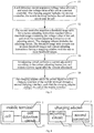
- Fig. 4 is a first block diagram showing a charging system provided by an embodiment of the present disclosure. For illustration purposes, only parts related to embodiments of the present disclosure are shown, which will be described in detail in the following.
- the charging system includes: a charging adapter 2 including a second controller 21 and an adjusting circuit 22, and a mobile terminal 1 including a cell detection circuit 11 and a cell.
- the cell detection circuit 11 is configured to acquire a voltage value of the cell, and to send the voltage value of the cell to the second controller 21.
- the second controller 21 is configured to search a threshold range table for a current adjusting instruction matched with a threshold range containing the voltage value of the cell, and to send the current adjusting instruction to the adjusting circuit 22.
- the threshold range table records one or more threshold ranges, and one or more current adjusting instructions having a one-to-one mapping relation with the one or more threshold ranges.
- the adjusting circuit 22 is configured to perform a current adjustment according to the current adjusting instruction, and to output a power signal after the current adjustment.
- Fig. 5 is a second block diagram showing a charging system provided by an embodiment of the present disclosure. For illustration purposes, only parts related to embodiments of the present disclosure are shown, which will be described in detail in the following.
- the adjusting circuit 22 includes a current detection circuit 221.
- the current detection circuit 221 is configured to detect a current value of the power signal outputted by the adjusting circuit 22, and to send the current value detected to the second controller 21.
- the second controller 21 is further configured to calculate a difference between the current value detected and a current value specified by the current adjusting instruction, and to send a calibration instruction to the adjusting circuit 22 if an absolute value of the difference calculated is greater than a difference threshold.
- the adjusting circuit 22 is further configured to calibrate the power signal according to a current difference specified by the calibration instruction, and to output a calibrated power signal.
- a current value of the calibrated power signal is equal to the current value specified by the current adjusting instruction.
- Fig. 6 is a third block diagram showing a charging system provided by an embodiment of the present disclosure. For illustration purposes, only parts related to embodiments of the present disclosure are shown, which will be described in detail in the following.
- the charging adapter 2 further includes a second charging interface 23, and the mobile terminal 1 further includes a first charging interface 12.
- the charging adapter 2 is further configured to send the power signal to the first charging interface 12 through the second charging interface 23, such that the charging adapter 2 charges the cell of the mobile terminal 1.
- a first power line in the first charging interface 12 is coupled to a second power line in the second charging interface 23, a first ground line in the first charging interface 12 is coupled to a second ground line in the second charging interface 23.
- P second power lines and Q second ground lines there are P second power lines and Q second ground lines.
- the P first power lines in the first charging interface 12 are connected respectively with the P second power lines in the second charging interface 23
- the Q first ground lines in the first charging interface 12 are connected respectively with the Q second ground lines in the second charging interface 23.
- Fig. 7 is a fourth block diagram showing a charging system provided by an embodiment of the present disclosure. For illustration purposes, only parts related to embodiments of the present disclosure are shown, which will be described in detail in the following.
- the cell detection circuit 11 includes a cell connector 112 and a first controller 111.
- the first controller 111 is configured to acquire the voltage value of the cell through the cell connector 112, and send the voltage value of the cell to the second controller 21.
Landscapes
- Engineering & Computer Science (AREA)
- Power Engineering (AREA)
- Charge And Discharge Circuits For Batteries Or The Like (AREA)
- Secondary Cells (AREA)
Priority Applications (1)
| Application Number | Priority Date | Filing Date | Title |
|---|---|---|---|
| EP19165440.9A EP3534487B1 (en) | 2014-01-28 | 2014-05-09 | Charging method and system |
Applications Claiming Priority (2)
| Application Number | Priority Date | Filing Date | Title |
|---|---|---|---|
| CN201410042717.2A CN103746434B (zh) | 2014-01-28 | 2014-01-28 | 充电方法和系统 |
| PCT/CN2014/077150 WO2015113339A1 (zh) | 2014-01-28 | 2014-05-09 | 充电方法和系统 |
Related Child Applications (2)
| Application Number | Title | Priority Date | Filing Date |
|---|---|---|---|
| EP19165440.9A Division EP3534487B1 (en) | 2014-01-28 | 2014-05-09 | Charging method and system |
| EP19165440.9A Division-Into EP3534487B1 (en) | 2014-01-28 | 2014-05-09 | Charging method and system |
Publications (3)
| Publication Number | Publication Date |
|---|---|
| EP3101760A1 EP3101760A1 (en) | 2016-12-07 |
| EP3101760A4 EP3101760A4 (en) | 2017-09-13 |
| EP3101760B1 true EP3101760B1 (en) | 2019-07-03 |
Family
ID=50503438
Family Applications (2)
| Application Number | Title | Priority Date | Filing Date |
|---|---|---|---|
| EP14881200.1A Active EP3101760B1 (en) | 2014-01-28 | 2014-05-09 | Charging method and system |
| EP19165440.9A Active EP3534487B1 (en) | 2014-01-28 | 2014-05-09 | Charging method and system |
Family Applications After (1)
| Application Number | Title | Priority Date | Filing Date |
|---|---|---|---|
| EP19165440.9A Active EP3534487B1 (en) | 2014-01-28 | 2014-05-09 | Charging method and system |
Country Status (7)
| Country | Link |
|---|---|
| US (4) | US10177587B2 (es) |
| EP (2) | EP3101760B1 (es) |
| CN (1) | CN103746434B (es) |
| DK (1) | DK3101760T3 (es) |
| ES (1) | ES2742867T3 (es) |
| PT (1) | PT3101760T (es) |
| WO (1) | WO2015113339A1 (es) |
Families Citing this family (16)
| Publication number | Priority date | Publication date | Assignee | Title |
|---|---|---|---|---|
| CN103746427A (zh) * | 2014-01-09 | 2014-04-23 | 小米科技有限责任公司 | 电源、电源充电电路、方法及终端设备 |
| CN103746434B (zh) | 2014-01-28 | 2016-04-06 | 广东欧珀移动通信有限公司 | 充电方法和系统 |
| CN103762690B (zh) * | 2014-01-28 | 2016-08-24 | 广东欧珀移动通信有限公司 | 充电系统 |
| EP3101770B1 (en) * | 2014-01-28 | 2019-05-15 | Guangdong Oppo Mobile Telecommunications Corp., Ltd | Power adapter and terminal |
| CN106716389B (zh) * | 2014-08-05 | 2020-04-10 | 德州仪器公司 | 用于快速usb充电的方法、电子装置及充电器设备 |
| EP3923443A1 (en) * | 2014-11-11 | 2021-12-15 | Guangdong Oppo Mobile Telecommunications Corp., Ltd. | Communication method, power adaptor and terminal |
| CN105098883A (zh) * | 2015-07-01 | 2015-11-25 | 深圳天珑无线科技有限公司 | 充电系统 |
| CN105098913A (zh) * | 2015-08-21 | 2015-11-25 | 上海传英信息技术有限公司 | 一种用于手持设备的3a快速充电系统及其充电方法 |
| CN105730265B (zh) * | 2016-01-21 | 2019-02-05 | 易事特集团股份有限公司 | 一种电动汽车的直流充电桩的充电启动装置 |
| KR102157343B1 (ko) | 2016-02-05 | 2020-09-17 | 광동 오포 모바일 텔레커뮤니케이션즈 코포레이션 리미티드 | 단말을 위한 충전 시스템, 충전 방법 및 전원 어댑터, 스위칭 전원 |
| CN105958581B (zh) * | 2016-05-31 | 2024-01-09 | 零度智控(北京)智能科技有限公司 | 充电方法、充电装置以及无人机 |
| CN107231014B (zh) * | 2016-09-20 | 2019-02-19 | 华为技术有限公司 | 一种充电电路、终端以及充电系统 |
| CN106410917B (zh) * | 2016-11-15 | 2019-05-03 | Oppo广东移动通信有限公司 | 充电系统及移动终端 |
| CN107645186A (zh) * | 2017-05-04 | 2018-01-30 | 合肥中耐电子设备有限公司 | 一种具备智能检测功能的充电器 |
| CN113824167B (zh) * | 2020-06-19 | 2024-04-30 | 青岛海信移动通信技术有限公司 | 一种充电电路和充电方法 |
| CN113851745A (zh) * | 2021-09-29 | 2021-12-28 | 东莞新能安科技有限公司 | 电芯充电控制方法、电池包以及并机系统 |
Citations (1)
| Publication number | Priority date | Publication date | Assignee | Title |
|---|---|---|---|---|
| CN102208702A (zh) * | 2011-05-06 | 2011-10-05 | 惠州Tcl移动通信有限公司 | 电池充电方法和电子装置 |
Family Cites Families (19)
| Publication number | Priority date | Publication date | Assignee | Title |
|---|---|---|---|---|
| JP2914259B2 (ja) * | 1995-12-14 | 1999-06-28 | 日本電気株式会社 | 携帯電子機器と携帯電子機器の充電制御方法 |
| US5684382A (en) * | 1996-07-19 | 1997-11-04 | Compaq Computer Corporation | Control of computer AC adapter output voltage via battery pack feedback |
| US6222347B1 (en) * | 1998-04-30 | 2001-04-24 | Apple Computer, Inc. | System for charging portable computer's battery using both the dynamically determined power available based on power consumed by sub-system devices and power limits from the battery |
| EP1128517A3 (en) * | 2000-02-24 | 2003-12-10 | Makita Corporation | Adapters for rechargeable battery packs |
| JP4728303B2 (ja) * | 2007-08-31 | 2011-07-20 | パナソニック株式会社 | 充電回路、及びこれを備えた電池パック、充電システム |
| JP4966998B2 (ja) * | 2009-06-18 | 2012-07-04 | パナソニック株式会社 | 充電制御回路、電池パック、及び充電システム |
| US8816648B2 (en) * | 2009-08-17 | 2014-08-26 | Apple Inc. | Modulated, temperature-based multi-CC-CV charging technique for Li-ion/Li-polymer batteries |
| US8319470B2 (en) * | 2010-02-12 | 2012-11-27 | Suncore, Inc. | Stand alone solar battery charger |
| JP2011217571A (ja) * | 2010-04-01 | 2011-10-27 | Sanyo Electric Co Ltd | 電池パック用充電器 |
| JP5369082B2 (ja) * | 2010-12-06 | 2013-12-18 | パナソニック株式会社 | 充電器、アダプタ及び充電システム |
| US8497737B2 (en) * | 2011-03-28 | 2013-07-30 | Infineon Technologies Ag | Amplifier circuit, mobile communication device and method for adjusting a bias of a power amplifier |
| CN102931693B (zh) * | 2011-08-10 | 2014-12-10 | 联发科技(新加坡)私人有限公司 | 充电控制方法、装置以及充电系统和便携式设备 |
| CN103199582B (zh) * | 2013-03-27 | 2016-02-03 | 广东欧珀移动通信有限公司 | 充电电流调整方法和装置 |
| CN103219762B (zh) * | 2013-04-01 | 2017-02-08 | 海能达通信股份有限公司 | 一种充电控制电路 |
| CN103219769B (zh) * | 2013-04-17 | 2015-12-02 | 广东欧珀移动通信有限公司 | 电池充电方法、电池充电系统及移动终端 |
| CN103236568B (zh) * | 2013-05-03 | 2016-03-30 | 努比亚技术有限公司 | 充电方法和充电系统 |
| CN103746434B (zh) | 2014-01-28 | 2016-04-06 | 广东欧珀移动通信有限公司 | 充电方法和系统 |
| CN104810879B (zh) * | 2014-01-28 | 2016-12-14 | 广东欧珀移动通信有限公司 | 快速充电方法和系统 |
| CN104810909B (zh) * | 2014-01-28 | 2016-09-28 | 广东欧珀移动通信有限公司 | 快速充电控制方法和系统 |
-
2014
- 2014-01-28 CN CN201410042717.2A patent/CN103746434B/zh active Active
- 2014-05-09 DK DK14881200.1T patent/DK3101760T3/da active
- 2014-05-09 EP EP14881200.1A patent/EP3101760B1/en active Active
- 2014-05-09 EP EP19165440.9A patent/EP3534487B1/en active Active
- 2014-05-09 ES ES14881200T patent/ES2742867T3/es active Active
- 2014-05-09 WO PCT/CN2014/077150 patent/WO2015113339A1/zh active Application Filing
- 2014-05-09 US US15/114,952 patent/US10177587B2/en active Active
- 2014-05-09 PT PT14881200T patent/PT3101760T/pt unknown
-
2017
- 2017-05-16 US US15/596,985 patent/US10135278B2/en active Active
-
2018
- 2018-10-04 US US16/152,350 patent/US10439420B2/en active Active
- 2018-11-29 US US16/204,769 patent/US10447058B2/en active Active
Patent Citations (1)
| Publication number | Priority date | Publication date | Assignee | Title |
|---|---|---|---|---|
| CN102208702A (zh) * | 2011-05-06 | 2011-10-05 | 惠州Tcl移动通信有限公司 | 电池充电方法和电子装置 |
Also Published As
| Publication number | Publication date |
|---|---|
| US20170250544A1 (en) | 2017-08-31 |
| EP3534487B1 (en) | 2020-04-22 |
| EP3101760A4 (en) | 2017-09-13 |
| DK3101760T3 (da) | 2019-09-02 |
| EP3534487A1 (en) | 2019-09-04 |
| EP3101760A1 (en) | 2016-12-07 |
| CN103746434B (zh) | 2016-04-06 |
| US20190036352A1 (en) | 2019-01-31 |
| ES2742867T3 (es) | 2020-02-17 |
| US10135278B2 (en) | 2018-11-20 |
| US10439420B2 (en) | 2019-10-08 |
| US10447058B2 (en) | 2019-10-15 |
| US20160344199A1 (en) | 2016-11-24 |
| WO2015113339A1 (zh) | 2015-08-06 |
| US10177587B2 (en) | 2019-01-08 |
| PT3101760T (pt) | 2019-09-10 |
| CN103746434A (zh) | 2014-04-23 |
| US20190109467A1 (en) | 2019-04-11 |
Similar Documents
| Publication | Publication Date | Title |
|---|---|---|
| US10447058B2 (en) | Charging method and system | |
| US10714950B2 (en) | Charging control method and charging device | |
| US10148113B2 (en) | Charging method, device and charging device | |
| EP3101436A1 (en) | Interface insertion anomaly detection circuit and method | |
| US9859726B2 (en) | Detection circuit and method for starting charging | |
| US20170222453A1 (en) | Device, apparatus and method for supporting multi-battery quick charge |
Legal Events
| Date | Code | Title | Description |
|---|---|---|---|
| PUAI | Public reference made under article 153(3) epc to a published international application that has entered the european phase |
Free format text: ORIGINAL CODE: 0009012 |
|
| STAA | Information on the status of an ep patent application or granted ep patent |
Free format text: STATUS: REQUEST FOR EXAMINATION WAS MADE |
|
| 17P | Request for examination filed |
Effective date: 20160708 |
|
| AK | Designated contracting states |
Kind code of ref document: A1 Designated state(s): AL AT BE BG CH CY CZ DE DK EE ES FI FR GB GR HR HU IE IS IT LI LT LU LV MC MK MT NL NO PL PT RO RS SE SI SK SM TR |
|
| AX | Request for extension of the european patent |
Extension state: BA ME |
|
| DAX | Request for extension of the european patent (deleted) | ||
| A4 | Supplementary search report drawn up and despatched |
Effective date: 20170817 |
|
| RIC1 | Information provided on ipc code assigned before grant |
Ipc: H02J 7/00 20060101AFI20170810BHEP |
|
| STAA | Information on the status of an ep patent application or granted ep patent |
Free format text: STATUS: EXAMINATION IS IN PROGRESS |
|
| 17Q | First examination report despatched |
Effective date: 20180611 |
|
| REG | Reference to a national code |
Ref country code: DE Ref legal event code: R079 Ref document number: 602014049677 Country of ref document: DE Free format text: PREVIOUS MAIN CLASS: H02J0007000000 Ipc: H02M0007040000 |
|
| GRAP | Despatch of communication of intention to grant a patent |
Free format text: ORIGINAL CODE: EPIDOSNIGR1 |
|
| STAA | Information on the status of an ep patent application or granted ep patent |
Free format text: STATUS: GRANT OF PATENT IS INTENDED |
|
| RIC1 | Information provided on ipc code assigned before grant |
Ipc: H02M 7/04 20060101AFI20181109BHEP Ipc: H02J 7/00 20060101ALI20181109BHEP |
|
| INTG | Intention to grant announced |
Effective date: 20181130 |
|
| GRAS | Grant fee paid |
Free format text: ORIGINAL CODE: EPIDOSNIGR3 |
|
| GRAA | (expected) grant |
Free format text: ORIGINAL CODE: 0009210 |
|
| STAA | Information on the status of an ep patent application or granted ep patent |
Free format text: STATUS: THE PATENT HAS BEEN GRANTED |
|
| AK | Designated contracting states |
Kind code of ref document: B1 Designated state(s): AL AT BE BG CH CY CZ DE DK EE ES FI FR GB GR HR HU IE IS IT LI LT LU LV MC MK MT NL NO PL PT RO RS SE SI SK SM TR |
|
| REG | Reference to a national code |
Ref country code: GB Ref legal event code: FG4D |
|
| REG | Reference to a national code |
Ref country code: CH Ref legal event code: EP Ref country code: AT Ref legal event code: REF Ref document number: 1152188 Country of ref document: AT Kind code of ref document: T Effective date: 20190715 |
|
| REG | Reference to a national code |
Ref country code: IE Ref legal event code: FG4D |
|
| REG | Reference to a national code |
Ref country code: DE Ref legal event code: R096 Ref document number: 602014049677 Country of ref document: DE |
|
| REG | Reference to a national code |
Ref country code: NL Ref legal event code: FP |
|
| REG | Reference to a national code |
Ref country code: DK Ref legal event code: T3 Effective date: 20190827 |
|
| REG | Reference to a national code |
Ref country code: PT Ref legal event code: SC4A Ref document number: 3101760 Country of ref document: PT Date of ref document: 20190910 Kind code of ref document: T Free format text: AVAILABILITY OF NATIONAL TRANSLATION Effective date: 20190820 |
|
| REG | Reference to a national code |
Ref country code: LT Ref legal event code: MG4D |
|
| RAP2 | Party data changed (patent owner data changed or rights of a patent transferred) |
Owner name: GUANGDONG OPPO MOBILE TELECOMMUNICATIONS CORP., LT |
|
| PG25 | Lapsed in a contracting state [announced via postgrant information from national office to epo] |
Ref country code: SE Free format text: LAPSE BECAUSE OF FAILURE TO SUBMIT A TRANSLATION OF THE DESCRIPTION OR TO PAY THE FEE WITHIN THE PRESCRIBED TIME-LIMIT Effective date: 20190703 Ref country code: NO Free format text: LAPSE BECAUSE OF FAILURE TO SUBMIT A TRANSLATION OF THE DESCRIPTION OR TO PAY THE FEE WITHIN THE PRESCRIBED TIME-LIMIT Effective date: 20191003 Ref country code: BG Free format text: LAPSE BECAUSE OF FAILURE TO SUBMIT A TRANSLATION OF THE DESCRIPTION OR TO PAY THE FEE WITHIN THE PRESCRIBED TIME-LIMIT Effective date: 20191003 Ref country code: LT Free format text: LAPSE BECAUSE OF FAILURE TO SUBMIT A TRANSLATION OF THE DESCRIPTION OR TO PAY THE FEE WITHIN THE PRESCRIBED TIME-LIMIT Effective date: 20190703 Ref country code: HR Free format text: LAPSE BECAUSE OF FAILURE TO SUBMIT A TRANSLATION OF THE DESCRIPTION OR TO PAY THE FEE WITHIN THE PRESCRIBED TIME-LIMIT Effective date: 20190703 Ref country code: CZ Free format text: LAPSE BECAUSE OF FAILURE TO SUBMIT A TRANSLATION OF THE DESCRIPTION OR TO PAY THE FEE WITHIN THE PRESCRIBED TIME-LIMIT Effective date: 20190703 Ref country code: FI Free format text: LAPSE BECAUSE OF FAILURE TO SUBMIT A TRANSLATION OF THE DESCRIPTION OR TO PAY THE FEE WITHIN THE PRESCRIBED TIME-LIMIT Effective date: 20190703 |
|
| REG | Reference to a national code |
Ref country code: ES Ref legal event code: FG2A Ref document number: 2742867 Country of ref document: ES Kind code of ref document: T3 Effective date: 20200217 |
|
| PG25 | Lapsed in a contracting state [announced via postgrant information from national office to epo] |
Ref country code: LV Free format text: LAPSE BECAUSE OF FAILURE TO SUBMIT A TRANSLATION OF THE DESCRIPTION OR TO PAY THE FEE WITHIN THE PRESCRIBED TIME-LIMIT Effective date: 20190703 Ref country code: AL Free format text: LAPSE BECAUSE OF FAILURE TO SUBMIT A TRANSLATION OF THE DESCRIPTION OR TO PAY THE FEE WITHIN THE PRESCRIBED TIME-LIMIT Effective date: 20190703 Ref country code: RS Free format text: LAPSE BECAUSE OF FAILURE TO SUBMIT A TRANSLATION OF THE DESCRIPTION OR TO PAY THE FEE WITHIN THE PRESCRIBED TIME-LIMIT Effective date: 20190703 Ref country code: IS Free format text: LAPSE BECAUSE OF FAILURE TO SUBMIT A TRANSLATION OF THE DESCRIPTION OR TO PAY THE FEE WITHIN THE PRESCRIBED TIME-LIMIT Effective date: 20191103 Ref country code: GR Free format text: LAPSE BECAUSE OF FAILURE TO SUBMIT A TRANSLATION OF THE DESCRIPTION OR TO PAY THE FEE WITHIN THE PRESCRIBED TIME-LIMIT Effective date: 20191004 |
|
| PG25 | Lapsed in a contracting state [announced via postgrant information from national office to epo] |
Ref country code: TR Free format text: LAPSE BECAUSE OF FAILURE TO SUBMIT A TRANSLATION OF THE DESCRIPTION OR TO PAY THE FEE WITHIN THE PRESCRIBED TIME-LIMIT Effective date: 20190703 |
|
| PG25 | Lapsed in a contracting state [announced via postgrant information from national office to epo] |
Ref country code: RO Free format text: LAPSE BECAUSE OF FAILURE TO SUBMIT A TRANSLATION OF THE DESCRIPTION OR TO PAY THE FEE WITHIN THE PRESCRIBED TIME-LIMIT Effective date: 20190703 Ref country code: PL Free format text: LAPSE BECAUSE OF FAILURE TO SUBMIT A TRANSLATION OF THE DESCRIPTION OR TO PAY THE FEE WITHIN THE PRESCRIBED TIME-LIMIT Effective date: 20190703 Ref country code: EE Free format text: LAPSE BECAUSE OF FAILURE TO SUBMIT A TRANSLATION OF THE DESCRIPTION OR TO PAY THE FEE WITHIN THE PRESCRIBED TIME-LIMIT Effective date: 20190703 |
|
| PG25 | Lapsed in a contracting state [announced via postgrant information from national office to epo] |
Ref country code: SM Free format text: LAPSE BECAUSE OF FAILURE TO SUBMIT A TRANSLATION OF THE DESCRIPTION OR TO PAY THE FEE WITHIN THE PRESCRIBED TIME-LIMIT Effective date: 20190703 Ref country code: SK Free format text: LAPSE BECAUSE OF FAILURE TO SUBMIT A TRANSLATION OF THE DESCRIPTION OR TO PAY THE FEE WITHIN THE PRESCRIBED TIME-LIMIT Effective date: 20190703 Ref country code: IS Free format text: LAPSE BECAUSE OF FAILURE TO SUBMIT A TRANSLATION OF THE DESCRIPTION OR TO PAY THE FEE WITHIN THE PRESCRIBED TIME-LIMIT Effective date: 20200224 |
|
| REG | Reference to a national code |
Ref country code: DE Ref legal event code: R097 Ref document number: 602014049677 Country of ref document: DE |
|
| PLBE | No opposition filed within time limit |
Free format text: ORIGINAL CODE: 0009261 |
|
| STAA | Information on the status of an ep patent application or granted ep patent |
Free format text: STATUS: NO OPPOSITION FILED WITHIN TIME LIMIT |
|
| PG2D | Information on lapse in contracting state deleted |
Ref country code: IS |
|
| 26N | No opposition filed |
Effective date: 20200603 |
|
| PG25 | Lapsed in a contracting state [announced via postgrant information from national office to epo] |
Ref country code: SI Free format text: LAPSE BECAUSE OF FAILURE TO SUBMIT A TRANSLATION OF THE DESCRIPTION OR TO PAY THE FEE WITHIN THE PRESCRIBED TIME-LIMIT Effective date: 20190703 |
|
| PG25 | Lapsed in a contracting state [announced via postgrant information from national office to epo] |
Ref country code: CH Free format text: LAPSE BECAUSE OF NON-PAYMENT OF DUE FEES Effective date: 20200531 Ref country code: MC Free format text: LAPSE BECAUSE OF FAILURE TO SUBMIT A TRANSLATION OF THE DESCRIPTION OR TO PAY THE FEE WITHIN THE PRESCRIBED TIME-LIMIT Effective date: 20190703 Ref country code: LI Free format text: LAPSE BECAUSE OF NON-PAYMENT OF DUE FEES Effective date: 20200531 |
|
| REG | Reference to a national code |
Ref country code: BE Ref legal event code: MM Effective date: 20200531 |
|
| PG25 | Lapsed in a contracting state [announced via postgrant information from national office to epo] |
Ref country code: LU Free format text: LAPSE BECAUSE OF NON-PAYMENT OF DUE FEES Effective date: 20200509 |
|
| PG25 | Lapsed in a contracting state [announced via postgrant information from national office to epo] |
Ref country code: IE Free format text: LAPSE BECAUSE OF NON-PAYMENT OF DUE FEES Effective date: 20200509 |
|
| PG25 | Lapsed in a contracting state [announced via postgrant information from national office to epo] |
Ref country code: BE Free format text: LAPSE BECAUSE OF NON-PAYMENT OF DUE FEES Effective date: 20200531 |
|
| REG | Reference to a national code |
Ref country code: AT Ref legal event code: UEP Ref document number: 1152188 Country of ref document: AT Kind code of ref document: T Effective date: 20190703 |
|
| PG25 | Lapsed in a contracting state [announced via postgrant information from national office to epo] |
Ref country code: MT Free format text: LAPSE BECAUSE OF FAILURE TO SUBMIT A TRANSLATION OF THE DESCRIPTION OR TO PAY THE FEE WITHIN THE PRESCRIBED TIME-LIMIT Effective date: 20190703 Ref country code: CY Free format text: LAPSE BECAUSE OF FAILURE TO SUBMIT A TRANSLATION OF THE DESCRIPTION OR TO PAY THE FEE WITHIN THE PRESCRIBED TIME-LIMIT Effective date: 20190703 |
|
| PG25 | Lapsed in a contracting state [announced via postgrant information from national office to epo] |
Ref country code: MK Free format text: LAPSE BECAUSE OF FAILURE TO SUBMIT A TRANSLATION OF THE DESCRIPTION OR TO PAY THE FEE WITHIN THE PRESCRIBED TIME-LIMIT Effective date: 20190703 |
|
| P01 | Opt-out of the competence of the unified patent court (upc) registered |
Effective date: 20230412 |
|
| PGFP | Annual fee paid to national office [announced via postgrant information from national office to epo] |
Ref country code: NL Payment date: 20230427 Year of fee payment: 10 |
|
| PGFP | Annual fee paid to national office [announced via postgrant information from national office to epo] |
Ref country code: PT Payment date: 20230417 Year of fee payment: 10 Ref country code: IT Payment date: 20230523 Year of fee payment: 10 Ref country code: FR Payment date: 20230523 Year of fee payment: 10 Ref country code: ES Payment date: 20230607 Year of fee payment: 10 Ref country code: DK Payment date: 20230427 Year of fee payment: 10 Ref country code: DE Payment date: 20230510 Year of fee payment: 10 |
|
| PGFP | Annual fee paid to national office [announced via postgrant information from national office to epo] |
Ref country code: AT Payment date: 20230421 Year of fee payment: 10 |
|
| PGFP | Annual fee paid to national office [announced via postgrant information from national office to epo] |
Ref country code: GB Payment date: 20230519 Year of fee payment: 10 |