EP3093648A1 - Particulate substance detection element, particulate substance detection sensor, and method for manufacturing particulate substance detection element - Google Patents
Particulate substance detection element, particulate substance detection sensor, and method for manufacturing particulate substance detection element Download PDFInfo
- Publication number
- EP3093648A1 EP3093648A1 EP15734833.5A EP15734833A EP3093648A1 EP 3093648 A1 EP3093648 A1 EP 3093648A1 EP 15734833 A EP15734833 A EP 15734833A EP 3093648 A1 EP3093648 A1 EP 3093648A1
- Authority
- EP
- European Patent Office
- Prior art keywords
- particulate matter
- conductor
- conductor layer
- end edge
- layers
- Prior art date
- Legal status (The legal status is an assumption and is not a legal conclusion. Google has not performed a legal analysis and makes no representation as to the accuracy of the status listed.)
- Withdrawn
Links
Images








Classifications
-
- G—PHYSICS
- G01—MEASURING; TESTING
- G01N—INVESTIGATING OR ANALYSING MATERIALS BY DETERMINING THEIR CHEMICAL OR PHYSICAL PROPERTIES
- G01N15/00—Investigating characteristics of particles; Investigating permeability, pore-volume or surface-area of porous materials
- G01N15/06—Investigating concentration of particle suspensions
- G01N15/0656—Investigating concentration of particle suspensions using electric, e.g. electrostatic methods or magnetic methods
-
- G—PHYSICS
- G01—MEASURING; TESTING
- G01M—TESTING STATIC OR DYNAMIC BALANCE OF MACHINES OR STRUCTURES; TESTING OF STRUCTURES OR APPARATUS, NOT OTHERWISE PROVIDED FOR
- G01M15/00—Testing of engines
- G01M15/04—Testing internal-combustion engines
- G01M15/10—Testing internal-combustion engines by monitoring exhaust gases or combustion flame
- G01M15/102—Testing internal-combustion engines by monitoring exhaust gases or combustion flame by monitoring exhaust gases
-
- G—PHYSICS
- G01—MEASURING; TESTING
- G01N—INVESTIGATING OR ANALYSING MATERIALS BY DETERMINING THEIR CHEMICAL OR PHYSICAL PROPERTIES
- G01N15/00—Investigating characteristics of particles; Investigating permeability, pore-volume or surface-area of porous materials
- G01N15/06—Investigating concentration of particle suspensions
- G01N15/0606—Investigating concentration of particle suspensions by collecting particles on a support
-
- G—PHYSICS
- G01—MEASURING; TESTING
- G01N—INVESTIGATING OR ANALYSING MATERIALS BY DETERMINING THEIR CHEMICAL OR PHYSICAL PROPERTIES
- G01N15/00—Investigating characteristics of particles; Investigating permeability, pore-volume or surface-area of porous materials
- G01N2015/0042—Investigating dispersion of solids
- G01N2015/0046—Investigating dispersion of solids in gas, e.g. smoke
Definitions
- the present disclosure relates to a particulate matter detection element favorably used for an exhaust gas purification system of a vehicle internal combustion engine to detect particulate matter present in an exhaust gas that is a gas to be measured, and relates to a particulate matter detection sensor, and a method of manufacturing the particulate matter detection element.
- Particulate matter detection sensors that detect particulate matter in various gases to be measured have been proposed.
- a pair of electrodes are formed on a surface of a substrate having insulating properties.
- the particulate matter detection sensor senses changes in electrical characteristics, such as resistance and capacitance, caused by particulate matter being deposited between the pair of electrodes to thereby detect the particulate matter contained in a gas to be measured, such as a combustion exhaust gas of an internal combustion engine.
- a patent literature JP-A-2008-502892 discloses a sensor element in which a pair of comb-shaped electrodes are formed on an insulated substrate such as of alumina ceramic.
- a voltage is applied across the pair of electrodes from a power supply unit to form a non-uniform electric field in a space between the comb-shaped electrodes meshing with each other.
- soot particles contained in an exhaust gas passing through the sensor element are attracted to the electrodes and deposited thereon. Detecting the resistance across the electrodes of this moment, the amount of deposited soot can be measured.
- a patent literature JP-A-S60-196659 discloses resistance measurement electrodes for use in a sensor.
- the resistance measurement electrodes have a laminated structure in which conductor layers and insulating layers are alternately laminated using thick-film printing and green sheets to accurately form electrodes with a distance of 50 ⁇ m or less therebetween, which has been difficult to achieve with conventional thick-film printing.
- a cross section of the laminated structure is used as the resistance measurement electrodes, with the conductor layers serving as the electrodes.
- the patent literature JP-A-S60-196659 discloses that the distance between the electrodes can be reduced to about 10 ⁇ m which is determined by the thickness of the insulating layer.
- a laminated structure can be formed by alternately laminating conductor layers and insulating layers, with the conductor layers being exposed to a cross section of the laminated structure for use as a pair of electrodes as disclosed in JP-A-2008-502892 .
- a voltage can be applied across the electrodes to form an electric field to deposit particulate matter between the electrodes as disclosed in JP-A-2008-502892 .
- electric charge is concentrated at corners of the electrode end portions.
- the present disclosure has as its object to provide a particulate matter detection element having a laminated structure in which flat-shaped conductor layers and flat-shaped insulating layers are alternately laminated, the structure having a cross section where the conductor layers are exposed as a pair of electrodes to configure a detecting unit, with each electrode layer end portion being in a characteristic shape to minimize electric field concentration thereon, to provide a particulate matter detection sensor that uses the particulate matter detection element to form an electric field by applying a high voltage across the pair of electrodes to collect particulate matter, while detecting electrical characteristics changing with the amount of particulate matter in a gas to be measured deposited between the electrodes to highly accurately detect the particulate matter, and to provide a method of manufacturing the particulate matter detection element that minimizes concentration of electric charge on the electrode end portion to realize high detection accuracy.
- a particulate matter detection element (10, 10a, 10c, 10d, 10f) of the present disclosure has a laminated structure in which flat-shaped conductor layers (11, 11a, 11c, 11d, 11f, 12, 12a, 12c, 12d, 12f) and flat-shaped insulating layers (100, 100a, 100c, 100c, 100d, 100f) are alternately laminated.
- a detecting unit 13, 13a, 13c, 13d, 13f having the conductor layers of different polarities as a pair of detection electrodes is configured. Electrical characteristics changing with the amount of particulate matter deposited in the detecting unit are measured and for use in detecting particulate matter in a gas to be measured.
- the particulate matter detection element is characterized in that the conductor layers each have a constant thickness, and include conductor layer planar portions (110, 110a, 110c, 110d, 110f, 120, 120a, 120c, 120d, 120f) having a stripped-pattern cross section, and tapered conductor layer end edge portions (111, 111a, 111c, 111d, 111f, 121, 121a, 121c, 121d, 121f) each having a triangular cross section, provided on both sides of the respective conductor layer planar portions.
- conductor layer planar portions 110, 110a, 110c, 110d, 110f, 120, 120a, 120c, 120d, 120f
- tapered conductor layer end edge portions 111, 111a, 111c, 111d, 111f, 121, 121a, 121c, 121d, 121f
- the conductor layers may also each have a constant thickness, and include conductor layer planar portions (110b, 110e, 110g, 120b, 120e, 120g) having a stripped-pattern cross section, and gently curved conductor layer end edge portions (111b, 111e, 111g, 121b, 121e, 121g) each having a circular-arc cross section, provided on both sides of the respective conductor layer planar portions.
- electric field concentration is minimized in the conductor layer end edge portions, and variation in insensible mass due to local deposition of particulate matter is minimized in electric field concentration portions. Therefore, a particulate matter detection element having stable detection accuracy can be realized.
- the particulate matter detection sensor 1 (hereafter referred to as sensor 1) of the present disclosure is configured by the particulate matter detection element 10 (hereafter referred to as element 10), a power supply 2, and a measuring unit 3.
- the element 10 includes a detecting unit 13 which is disposed in a gas to be measured that is an exhaust gas of an internal combustion engine.
- the power supply 2 applies a predetermined voltage to the element 10.
- the measuring unit 3 measures electrical characteristics, such as changes in current flowing through the element 10, and changes in voltage and impedance of the element 10, to detect particulate matter in the gas to be measured.
- the element 10 side provided with the detecting unit 13 and exposed to the gas to be measured is referred to as a tip end side.
- the element 10 side connected to the power supply 2 and the measuring unit 3 is referred to as a base end side.
- the sensor 1 can be arranged downstream of a diesel particulate filter (DPF) to detect abnormality of the DPF.
- DPF diesel particulate filter
- the sensor 1 can be arranged upstream of the DPF and used in a system that directly detects particulate matter PM flowing into the DPF.
- a known configuration commonly used as a particulate matter detection sensor including a housing or a cover protecting the detecting unit 13, not shown, can be appropriately used to fix the element 10.
- the element 10 has a laminated structure in which flat-shaped conductor layers 11 and 12 and flat-shaped insulating layers 100 are alternately laminated.
- the element 10 uses its cross section to configure the detecting unit 13 where the conductor layers 11 and 12 having differing polarities form a pair of detection electrodes.
- the detecting unit 13 is configured such that the cross sections of the conductor layers 11 and 12 are alternated, with the insulating layer 100 being interposed between each pair of the conductor layers 11 and 12.
- the conductor layers 11 and 12 are characterized in that they each have a constant thickness and include respective conductor layer planar portions 110 and 120 (hereafter referred to as planar portions 110 and 120) and respective conductor layer end edge portions 111 and 121 (hereafter referred to as end edge portions 111 and 121).
- the planar portions 110 and 120 have cross sections in a stripped pattern.
- the end edge portions 111 and 112, which are each tapered and have a triangular cross section, are provided to both sides of the respective conductor layer planar portions 110 and 120.
- the present disclosure can reduce electric field concentration at the end edges of the conductor layers 11 and 12.
- particulate matter is prevented from being locally deposited on electric field concentration portions (i.e., portions where electric field is concentrated) and detection accuracy is improved and stabilized.
- conductive materials can be used as appropriate for the conductor layers 11 and 12.
- conductive materials that can be used include metal materials such as aluminum, gold, platinum, and tungsten, metal oxide materials such as ruthenium oxide, and any perovskite-type conductive oxide material selected from LNF (LaNi 0.6 Fe 0.4 O 3 ), LSN (LaNi 0.6 Fe 0.4 O 3 ), LSM (La 1-X Sr X MnO 3- ⁇ ), LSC (La 1-X SrXCoO 3- ⁇ ), LCC (La 1-X Ca X CrO 3- ⁇ ), and LSCN (La 0.85 Sr 0.15 Cr 1-X Ni X O 3- ⁇ ) (0.1 ⁇ X ⁇ 0.7).
- insulating layer materials such as alumina, magnesia, titania and mullite, dielectric materials each being a mixture of a high-dielectric constant material, such as barium titanate, with alumina or zirconia, and known ceramic materials such as partially stabilized zirconia, represented by 8YSZ (ZrO 2 ) 0.82 (Y 2 O 3 ) 0.08 ).
- the present embodiment shows an example in which the detecting unit 13 is formed such that the cross sections of the pair of conductor layers 11 and 12 are exposed parallel to a lateral face on the tip end side of the particulate matter detection element 10 in a rectangular parallelepiped shape.
- the detecting unit 13 may be provided such that the cross sections of the pair of conductor layers 11 and 12 are exposed from a bottom surface on the tip end side of the element 10.
- FIGs. 1A to 1C different hatchings are used to clarify that the pair of conductor layers 11 and 12 are alternately laminated and the polarities are alternated. The different hatchings are not used for discriminating the materials of the conductor layers 11 and 12.
- the insulating layer 100 is formed into a flat shape by a known manufacturing method, such as doctor blading, with through holes being punched, as necessary, in predetermined positions to thereby form through hole electrodes 114 and 124.
- the pair of conductor layers 11 and 12 are configured by the planar portions 110 and 120 which are provided with the end edge portions 111 and 121 using a manufacturing method described hereafter, lead portions 112 and 122 connected to the outside, terminal portions 113 and 123, and through hole electrodes 114, 124, and 125.
- the through hole electrodes 114 and 124 electrically conduct the planar portions 110 and 120 having the same polarity.
- the lead portions 112 and 122, the through hole electrodes 114 and 124, and the terminal portions 113 and 123 are formed by a manufacturing method, such as known thick-film printing.
- a laminated structure is used for the element 10. Specifically, in the laminated structure, several conductor layers 11 and 12 are laminated on respective insulating layers 100 such that the conductor layers 11 and 12 are alternated.
- the present embodiment includes a lowermost insulating layer 100H which is provided with a heating element 140 that generates heat by energization and a pair of lead 141 and terminal 142 for electrically conducting the heating element 140, thereby configuring a heating unit 14.
- a known heating resistor material such as tungsten, molybdenum silicide, or ruthenium oxide is used.
- a known electrically conductive metal material such as gold, platinum, or tungsten is used.
- a known method, such as thick-film printing, is used for forming these components.
- the element 10 is integrally formed by baking.
- the element 10 after being laminated and baked, is appropriately cut such that a cross section thereof is exposed to a lateral side face thereof, followed by polishing.
- a basic structure of both the comparative examples and the examples is a laminated structure similar to that of example 1 shown in Fig. 1C .
- corresponding portions are represented by reference signs suffixed with z, y, x, and w for comparative examples 1, 2, 3, and 4, and suffixed with a to g for examples 2 to 8.
- insulating layers 100z are laminated with respective conductor layers 110z and conductor layers 120z, such that the conductor layers 110z are alternated with the conductor layers 120z.
- the conductor layers 110z and 120z of the comparative example 1 each have a rectangular cross section, with end faces being in a square shape and aligned.
- the insulating layers 100 are laminated with the respective conductor layers 110 and the conductor layers 120, such that the conductor layers 110 are alternated with the conductor layers 120.
- the conductor layers 110 and 120 of example 1 have the tapered end edge portions 111 and 121, respectively, which have a triangular (obtuse angle) cross section and are aligned.
- An element 10a shown in Fig. 2C as example 2 is different from example 1 in that end edge portions 111a and 121a have an acute triangular cross section.
- An element 10b shown in Fig. 2D as example 3 is different from example 1 in that end edge portions 111b and 121b are curved and have a circular-arc cross section.
- the element 10b is characterized in that the conductor layers each have a constant thickness, and include respective conductor layer planar portions 110b and 120b in a stripped pattern in the cross section of the element, and smoothly curved conductor layer end edge portions 111b and 121b having a circular arc cross section, provided on both sides of the respective conductor layer planar portions.
- conductor layers 110y and 120y have square end faces similarly to comparative example 1.
- the element 10y is different from comparative example 1 in that the end faces are not aligned.
- conductor layers 110c and 120c are provided with tapered end edge portions 111c and 121c having a triangular (obtuse angle) cross section similarly to example 1.
- the element 10c are different from example 1 in that the end edge portions 111c and 121c are not aligned.
- conductor layers 110d and 120d are provided with tapered end edge portions 111d and 121d having a triangular (acute angle) cross section similarly to in example 2.
- the element 10d is different from example 2 in that the end edge portions 111d and 121d are not aligned.
- curved end edge portions 111e and 121e have a circular-arc cross section similarly to example 3.
- the element 10e is different from example 3 in that the end edge portions 111e and 121e are not aligned.
- examples 4 and 5 it has been found that more electric field concentration is caused than in examples 1 and 2, and the electric field intensity in the areas between the planar portions 110c and 110d, and between 120c and 120d in which the electric field intensity is uniform becomes relatively lower than in examples 1 and 2.
- example 6 it has been found that the electric field concentration is more reduced than in example 3, and the electric field intensity in the area between the planar portions 110e and 120e in which the electric field intensity is uniform becomes relatively higher than in example 3.
- a shielding layer 14 is provided to the detecting unit 13f to cover all the end edge portions 111f and 121f and part of the planar portions 110f and 120f, that is to say, to cover the areas where the electric field intensity is non-uniform.
- the shielding layer 14 is made of a known insulating material, such as glass or alumina, or the same material as the insulating layer 100.
- the configuration provided with the shielding layer 14 can also be used in any of the foregoing examples 1 to 6.
- Figs. 7A and 7B the results of the tests conducted to confirm the advantageous effects of the present disclosure will be described.
- the detecting unit 13 of the element 10 is located in a flow path of a gas to be measured and exposed to a gas, with a predetermined voltage being applied to the detecting unit 13 from the power supply 2, and with a known amount of particulate matter being permitted to flow.
- example 1 it has been found that the average value ⁇ 1 of the insensible masses Q 0 is greater than that of the insensible masses in comparative example 1, but the variation ⁇ 1 between the samples is much smaller.
- each sample is evaluated by calculating a variation coefficient CV (100 ⁇ 2 / ⁇ ) (%).
- the evaluation results are shown in Fig. 7B .
- the variation in comparative example 2 is smaller than in comparative example 1 but, in all examples 1 to 7, the variation coefficient can be made smaller than in comparative examples 1 to 4.
- the present disclosure has an effect of improving reliability as a sensor.
- concentration of the electric field and local deposition of particulate matter in the end portions of the conductor layers 11 and 12 are reduced by providing the end edge portions 111, 121, 111a, 121a, 111b, 121b, 111c, 121c, 111d, 121d, 111e, and 121e having a triangular or circular-arc cross section to both end faces of the respective conductor layers 11 and 12.
- Comparative example 1 shows a basic method of manufacturing the particulate matter detection element 10z in which a cross section of the alternate lamination of the conductor layers 11z and 12z and the insulating layers 100z is used as the detecting unit 13z.
- An insulating material such as alumina
- a known binder, plasticizer, dispersant, solvent, and the like is mixed with a known binder, plasticizer, dispersant, solvent, and the like, and stirred to form a slurry.
- the slurry is formed into a sheet shape by a known manufacturing method, such as doctor blading, thereby obtaining an insulating sheet 100zGS.
- the insulating sheet 100zGS is punched using a die or the like to form in advance, as required, an alignment guide for printing, through holes for embedding through hole electrodes 114z and 124z that connect conductor layers of the same polarity, and the like, and the insulating sheet 100zGS is punched out into a predetermined outer shape.
- a conductor paste is injected from a thick-film printing screen in which a predetermined conductor pattern is formed to transfer conductor layer printed films 11zPRT and 12zPRT to the insulating layer sheets 100zGS.
- intermediate layer 101z is formed by thick-film printing, using a paste containing the same materials as the insulating material for forming the insulating layer 100z, so as to cover portions except for the conductor layers.
- the intermediate layer 101z has the same thickness as that of the conductor layer printed films 11zPRT and 12zPRT.
- the insulating layer sheets 100zGS are laminated such that the polarities of the conductor layer printed films 11zPRT and 12zPRT are alternated, followed by pressure-bonding using a die or the like.
- a laminated structure obtained in this way is integrated by simultaneously baking the conductor layers 11z and 12z and the insulating layers 100z.
- the integrated object is cut and polished, for example, to expose cross sections of the conductor layers 11z and 12z forming the detecting unit 13, thereby completing the element 10z.
- the element 10y shown as comparative example 2 is based on a manufacturing method similar to that of comparative example 1.
- the conductor layers 11y and 12y are laminated with the end faces thereof being misaligned as designed.
- FIG. 8B an outline of a manufacturing process for the element 10x as comparative example 3 and problems of comparative example 3 will be described.
- Conductor layer printed films 11xPRT and 12xPRT are harder than the insulating layer sheets 100xGS. Therefore, in the laminating and pressure-bonding step P2x, the insulating layer sheets 100xGS are elastically deformed when they are laminated and pressure-bonded. Resultantly, the insulating layer sheets 100xGS are adhered to each other, embedding the conductor layer printed films 11xPRT and 12xPRT therebetween.
- gaps each having a triangular cross section are formed on both sides of the conductor layer printed films 11xPRT and 12xPRT.
- the laminated body is sintered and the gaps are reduced as a result of the surface areas of the gaps being reduced.
- the gaps are not completely eliminated and some remains as voids. Thus, there is a concern that the gaps can trigger delamination.
- the end faces of the conductor layers 11x and 12x after baking become polygonal or irregularly shaped.
- concentration of the electric field at the corners is easily caused.
- a recessed sheet 100PCD is formed in the punching step P0.
- the recessed sheet 100PCD is provided with a recess 101 at the position corresponding to the position where the conductor layer 110 or 120 is formed by printing.
- the recess 101 is in conformity with the predetermined shape of the conductor layer end edge portion 111 or 112.
- the punching die is provided with a protrusion for forming the recess 101, and the surface of the insulating layer sheet 100GS is pressed against the die.
- a tapered surface that is sloped at a desired angle can be formed in the portion in which the conductor layer end edge portion 111 or 121 is formed.
- the conductor layer end edge portion 111 or 121 side to be in contact with the insulating layer sheet 100GS is sloped conforming to the shape of the recess 101.
- the recess 101 is also formed on the underside of the recessed sheet 100PCD, when the recessed sheets are laminated in the laminating and pressure-bonding step P1, adhesion is improved between the conductor layer printed films 110 and 120, forming no voids, unlike in comparative example 2.
- the insulating layer sheets 100GS can be easily adhered to each other.
- the conductor layer end edge portions 111 and 121 can be formed into a tapered shape having a triangular cross section, the element 10 that can reduce concentration of the electric field can be easily realized.
- a conductor printing step P1a according to the present embodiment is different from the foregoing embodiments in that partially changed opening-ratio printing screens PPM and PPMA are used when the conductor layers 11 and 12 are printed on the insulating layer sheet 100(GS).
- a mesh opening ratio is partially changed such that the film thickness resulting from the printing is reduced at predetermined positions.
- the partially changed opening-ratio printing screens PPM and PPMA will be described.
- the partially changed opening-ratio printing screen PPM used can reduce the amount of conductor paste injected from the portions where the opening ratio is designed to be low.
- the thickness of the conductor layer formed can be reduced, enabling formation of the conductor layer end edge portions 111a and 112a tapered outward with acutely-angled sloped surfaces and having a triangular cross section.
- the conductor layers 11a and 12a having the conductor layer end edge portions 111a and 121a with a triangular cross section are formed in the insulating layer sheets 100GS. Further the insulating layer sheets 100GS are laminated and pressure-bonded using a die or the like. Thus, the insulating layers 100GS are brought into intimate contact with each other, embedding the conductor layers 11a and 12a therebetween.
- the laminated structure prepared in this way is baked in a baking step P3a.
- the element 10a reducing concentration of the electric field near the conductor end faces can be quite easily formed.
- a partially reduced opening-ratio screen M used in manufacturing the particulate matter detection element 10 of the present disclosure, and the shape of the conductor layers 11 and 12 formed by using the screen M.
- drawings to be referred to show only a pattern for forming the conductor layer planar portion 110 and the conductor layer end edge portion 111 in one of the pair of conductor layers 11 and 12.
- the pattern for forming the conductor layer planar portion 120 and the conductor layer end edge portion 121 of the other conductor layer corresponds to a left-and-right reverse of the pattern of the firstly mentioned conductor layer. Therefore, the following description is provided omitting the secondly mentioned conductor layer and using a combined reference sign 110/120 for the common configuration.
- the partially reduced opening-ratio screen M used in the present embodiment is obtained by partially rolling and smoothing a thick-film printing screen generally used in thick-film printing and by reducing a mesh thickness and mesh opening ratio.
- a resist film R is formed into a predetermined printed pattern by coating an emulsion onto a printing screen, followed by exposure with a pattern conforming to the configuration of the conductor layer planar portions 110 and 120, and further followed by curing.
- portions where the conductor layer end edge portions 111 and 121 are printed have a large thickness in the cross-sectional direction and a large line width in the planar direction. Therefore, the opening ratio of the portions where the conductor layer end edge portions 111 and 121 are printed, that is, opening ratios P 111 and P 121 for forming the end edge portions are lower than the opening ratio of a mask M1 used for portions where the conductor layer planar portion 110 is formed, that is, opening efficiency P 111 and P 121 of forming a planar portion.
- an opening ratio P 111 A / P 121 A for forming an end edge portion can be design to be lower than an opening ratio P 110 A / P 120 A for forming a planar portion, by increasing a weave density of lateral and vertical threads of a mask M2A for printing the conductor layer end edge portions 111 and 121, compared to a mask M1A for printing the conductor layer planar portions 110 and 120.
- the resist R is formed into a predetermined conductor pattern on a screen mesh whose opening ratio is partially adjusted in advance.
- the amount of conductor paste injected from the mask M2A is reduced in the conductor layer end edge portions 111 and 121, thereby forming the conductor layer end edge portions 111 and 121 with a thickness smaller than the conductor layer planar portions 110 and 120. Further, by gradually increasing the weave density outward, the conductor layer end edge portions 111 and 121 can be gradually thinned outward, thereby forming the tapered end edge portions with a triangular cross section.
- the conductor layers 11 and 12 have been laminated and pressure-bonded after being dried, as an example.
- the conductor layers 11 and 12 may be laminated and pressure-bonded in an undried state.
- the conductor layer end edge portions 111 and 121 can be formed into a desired shape.
- the intermediate layer 101 made of an insulating material as in comparative example 1 is not used in the laminating and pressure-bonding process P3.
- the intermediate layer 101 may be printed using a paste made of an insulating material, in the printing step.
- Use of the intermediate layer 101 can mitigate the shear stress applied to the insulating layer sheet 100 during lamination and pressure-bonding, or can improve mechanical strength of the element 10, or can minimize formation of cracks in the baking step.
Landscapes
- Chemical & Material Sciences (AREA)
- General Physics & Mathematics (AREA)
- Physics & Mathematics (AREA)
- Biochemistry (AREA)
- Life Sciences & Earth Sciences (AREA)
- Analytical Chemistry (AREA)
- Health & Medical Sciences (AREA)
- General Health & Medical Sciences (AREA)
- Dispersion Chemistry (AREA)
- Immunology (AREA)
- Pathology (AREA)
- Engineering & Computer Science (AREA)
- Combustion & Propulsion (AREA)
- Investigating Or Analyzing Materials By The Use Of Electric Means (AREA)
- Measuring Oxygen Concentration In Cells (AREA)
Abstract
Description
- The present disclosure relates to a particulate matter detection element favorably used for an exhaust gas purification system of a vehicle internal combustion engine to detect particulate matter present in an exhaust gas that is a gas to be measured, and relates to a particulate matter detection sensor, and a method of manufacturing the particulate matter detection element.
- Particulate matter detection sensors that detect particulate matter in various gases to be measured have been proposed. In such a particulate matter detection sensor, a pair of electrodes are formed on a surface of a substrate having insulating properties. Taking advantage of particulate matter having electrical conductivity, the particulate matter detection sensor senses changes in electrical characteristics, such as resistance and capacitance, caused by particulate matter being deposited between the pair of electrodes to thereby detect the particulate matter contained in a gas to be measured, such as a combustion exhaust gas of an internal combustion engine.
- For example, a patent literature
JP-A-2008-502892 - In the sensor element of the patent literature mentioned above, a voltage is applied across the pair of electrodes from a power supply unit to form a non-uniform electric field in a space between the comb-shaped electrodes meshing with each other. Thus, soot particles contained in an exhaust gas passing through the sensor element are attracted to the electrodes and deposited thereon. Detecting the resistance across the electrodes of this moment, the amount of deposited soot can be measured.
- On the other hand, a patent literature
JP-A-S60-196659 JP-A-S60-196659 -
- [PTL 1]
JP-A-2008-502892 - [PTL 2]
JP-A-S60-196659 - A laminated structure can be formed by alternately laminating conductor layers and insulating layers, with the conductor layers being exposed to a cross section of the laminated structure for use as a pair of electrodes as disclosed in
JP-A-2008-502892 JP-A-2008-502892 - It has been found that such electric charge concentration tends to cause particulate matter to be locally deposited near the electrode end portions where electric field intensity is high. Thus, there is a concern that the differences between the masses to which the detection is sensitive and insensitive is increased and detection accuracy is deteriorated.
- In light of the circumstances set forth above, the present disclosure has as its object to provide a particulate matter detection element having a laminated structure in which flat-shaped conductor layers and flat-shaped insulating layers are alternately laminated, the structure having a cross section where the conductor layers are exposed as a pair of electrodes to configure a detecting unit, with each electrode layer end portion being in a characteristic shape to minimize electric field concentration thereon, to provide a particulate matter detection sensor that uses the particulate matter detection element to form an electric field by applying a high voltage across the pair of electrodes to collect particulate matter, while detecting electrical characteristics changing with the amount of particulate matter in a gas to be measured deposited between the electrodes to highly accurately detect the particulate matter, and to provide a method of manufacturing the particulate matter detection element that minimizes concentration of electric charge on the electrode end portion to realize high detection accuracy.
- A particulate matter detection element (10, 10a, 10c, 10d, 10f) of the present disclosure has a laminated structure in which flat-shaped conductor layers (11, 11a, 11c, 11d, 11f, 12, 12a, 12c, 12d, 12f) and flat-shaped insulating layers (100, 100a, 100c, 100c, 100d, 100f) are alternately laminated. Using a cross section of the laminated structure, a detecting unit (13, 13a, 13c, 13d, 13f) having the conductor layers of different polarities as a pair of detection electrodes is configured. Electrical characteristics changing with the amount of particulate matter deposited in the detecting unit are measured and for use in detecting particulate matter in a gas to be measured. The particulate matter detection element is characterized in that the conductor layers each have a constant thickness, and include conductor layer planar portions (110, 110a, 110c, 110d, 110f, 120, 120a, 120c, 120d, 120f) having a stripped-pattern cross section, and tapered conductor layer end edge portions (111, 111a, 111c, 111d, 111f, 121, 121a, 121c, 121d, 121f) each having a triangular cross section, provided on both sides of the respective conductor layer planar portions.
- In the present disclosure, the conductor layers may also each have a constant thickness, and include conductor layer planar portions (110b, 110e, 110g, 120b, 120e, 120g) having a stripped-pattern cross section, and gently curved conductor layer end edge portions (111b, 111e, 111g, 121b, 121e, 121g) each having a circular-arc cross section, provided on both sides of the respective conductor layer planar portions.
- According to the present disclosure, electric field concentration is minimized in the conductor layer end edge portions, and variation in insensible mass due to local deposition of particulate matter is minimized in electric field concentration portions. Therefore, a particulate matter detection element having stable detection accuracy can be realized.
- In the accompanying drawings:
-
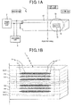
Fig. 1A is a schematic diagram illustrating a general configuration of a particulatematter detection sensor 1, according to a first embodiment of the present disclosure; -
Fig. 1B is an enlarged perspective view illustrating a detectingunit 13 that is a major part of a particulatematter detection element 10 used in the particulatematter detection sensor 1 illustrated inFig. 1A ; -
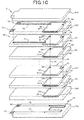
Fig. 1C is an exploded perspective view illustrating an example of an inner structure of the particulatematter detection element 10 used in the particulatematter detection sensor 1 illustratedFig. 1A ; -
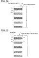
Fig. 2A is an enlarged view illustrating a major part of a conventional particulatematter detection element 10z in which an electrode layer end face is in a square shape, according to comparative example 1; -
Fig. 2B is an enlarged view illustrating a major part of the particulatematter detection element 10 in which an electrode layer end face is in an obtuse-angle triangular shape, given as example 1 of the present disclosure; -
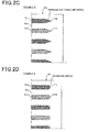
Fig. 2C is an enlarged view illustrating a major part of a particulatematter detection element 10a in which an electrode layer end face is in an acute triangular shape, according to example 2 of the present disclosure; -
Fig. 2D is an enlarged view illustrating a major part of a particulate matter detection element 10b in which an electrode layer end face is in a circular-arc shape, according to example 3 of the present disclosure; -
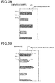
Fig. 3A is an enlarged view illustrating a major part of a conventional particulatematter detection element 10y in which an electrode layer end face is in a square shape and the end face position is not fixed, according to comparative example 2; -
Fig. 3B is an enlarged view illustrating a major part of a particulatematter detection element 10c in which an electrode layer end face is in an obtuse triangular shape and the end face position is not fixed, according to example 4 of the present disclosure; -
Fig. 3C is an enlarged view illustrating a major part of a particulatematter detection element 10d in which an electrode layer end face is in an acute triangular shape and the end face position is not fixed, according to example 5 of the present disclosure; -
Fig. 3D is an enlarged view illustrating a major part of a particulatematter detection element 10e in which an electrode layer end face is in a circular-arc shape and the end face position is not fixed, according to example 6 of the present disclosure; -
Fig. 4A is a schematic diagram illustrating electric field intensity distribution on a detecting unit plane, according to comparative example 1; -
Fig. 4B is a schematic diagram illustrating electric field intensity distribution on a detecting unit plane, according to example 1; -
Fig. 4C is a schematic diagram illustrating electric field intensity distribution on a detecting unit plane, according to example 2; -
Fig. 4D is a schematic diagram illustrating electric field intensity distribution on a detecting unit plane, according to example 3; -
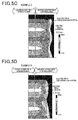
Fig. 5A is a schematic diagram illustrating electric field intensity distribution on a detecting unit plane, according to comparative example 2; -
Fig. 5B is a schematic diagram illustrating electric field intensity distribution on a detecting unit plane, according to example 4; -
Fig. 5C is a schematic diagram illustrating electric field intensity distribution on a detecting unit plane, according to example 5; -
Fig. 5D is a schematic diagram illustrating electric field intensity distribution on a detecting unit plane, according to example 6; -
Fig. 6 is an enlarged schematic perspective view illustrating a detectingunit 13f, according to example 7; -
Fig. 7A is a characteristics diagram illustrating variation in sensor output, according to comparative example 1 and example 1; -
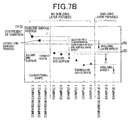
Fig. 7B is a characteristics diagram illustrating effects of reducing variation of insensible mass, according to several comparative examples and the present disclosure; -
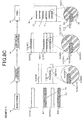
Fig. 8A is a schematic diagram illustrating a manufacturing process, according to comparative example 1; -
Fig. 8B is a schematic diagram illustrating a manufacturing process, according to comparative example 3; -
Fig. 8C is a schematic diagram illustrating a manufacturing process, according to example 1 of the present disclosure; -
Fig. 8D is a schematic diagram illustrating a manufacturing process, according to example 2 of the present disclosure; -
Fig. 9A is a schematic plan view illustrating a thick-film printing screen used in manufacturing the particulate matter detection element of the present disclosure; -
Fig. 9B is a set of diagrams including a cross-sectional view taken along the line B-B ofFig. 9A , and cross-sectional and plan views illustrating an insulating layer with a conductor layer being formed corresponding to the B-B cross-sectional view; and -
Fig. 10 is a plan view illustrating a modification of the thick-film printing screen used in the present disclosure. - With reference to
Figs. 1A, 1B , and1C , hereinafter is described an outline of a particulatematter detection sensor 1 according to a first embodiment of the present disclosure and a particulatematter detection element 10 that is a major part of the present disclosure. - The particulate matter detection sensor 1 (hereafter referred to as sensor 1) of the present disclosure is configured by the particulate matter detection element 10 (hereafter referred to as element 10), a
power supply 2, and ameasuring unit 3. Theelement 10 includes a detectingunit 13 which is disposed in a gas to be measured that is an exhaust gas of an internal combustion engine. Thepower supply 2 applies a predetermined voltage to theelement 10. The measuringunit 3 measures electrical characteristics, such as changes in current flowing through theelement 10, and changes in voltage and impedance of theelement 10, to detect particulate matter in the gas to be measured. - Electrical characteristics changing with the amount of particulate matter deposited in the detecting
unit 13 of theelement 10 are measured by the measuringunit 3 to detect particulate matter in the gas to be measured. - In the description hereinafter, the
element 10 side provided with the detectingunit 13 and exposed to the gas to be measured is referred to as a tip end side. Theelement 10 side connected to thepower supply 2 and the measuringunit 3 is referred to as a base end side. - The
sensor 1 can be arranged downstream of a diesel particulate filter (DPF) to detect abnormality of the DPF. Alternatively, thesensor 1 can be arranged upstream of the DPF and used in a system that directly detects particulate matter PM flowing into the DPF. - When the
sensor 1 is actually arranged in a flow path of a gas to be measured, a known configuration commonly used as a particulate matter detection sensor including a housing or a cover protecting the detectingunit 13, not shown, can be appropriately used to fix theelement 10. - Referring to
Fig. 1B , characteristics of theelement 10 that is a major part of the present disclosure will be specifically described. - The
element 10 has a laminated structure in which flat-shaped conductor layers 11 and 12 and flat-shaped insulatinglayers 100 are alternately laminated. - The
element 10 uses its cross section to configure the detectingunit 13 where the conductor layers 11 and 12 having differing polarities form a pair of detection electrodes. - As shown in
Fig. 1B , the detectingunit 13 is configured such that the cross sections of the conductor layers 11 and 12 are alternated, with the insulatinglayer 100 being interposed between each pair of the conductor layers 11 and 12. - According to the present embodiment, the conductor layers 11 and 12 are characterized in that they each have a constant thickness and include respective conductor layer
planar portions 110 and 120 (hereafter referred to asplanar portions 110 and 120) and respective conductor layerend edge portions 111 and 121 (hereafter referred to asend edge portions 111 and 121). Theplanar portions end edge portions planar portions - Since the conductor layer
end edge portions - Known conductive materials can be used as appropriate for the conductor layers 11 and 12. For example, conductive materials that can be used include metal materials such as aluminum, gold, platinum, and tungsten, metal oxide materials such as ruthenium oxide, and any perovskite-type conductive oxide material selected from LNF (LaNi0.6Fe0.4O3), LSN (LaNi0.6Fe0.4O3), LSM (La1-XSrXMnO3-δ), LSC (La1-XSrXCoO3-δ), LCC (La1-XCaXCrO3-δ), and LSCN (La0.85Sr0.15Cr1-XNiXO3-δ) (0.1 ≤ X ≤ 0.7).
- Materials that can be used, as appropriate, for the insulating
layer 100 include insulating layer materials such as alumina, magnesia, titania and mullite, dielectric materials each being a mixture of a high-dielectric constant material, such as barium titanate, with alumina or zirconia, and known ceramic materials such as partially stabilized zirconia, represented by 8YSZ (ZrO2)0.82(Y2O3)0.08). - The present embodiment shows an example in which the detecting
unit 13 is formed such that the cross sections of the pair of conductor layers 11 and 12 are exposed parallel to a lateral face on the tip end side of the particulatematter detection element 10 in a rectangular parallelepiped shape. However, the detectingunit 13 may be provided such that the cross sections of the pair of conductor layers 11 and 12 are exposed from a bottom surface on the tip end side of theelement 10. - In
Figs. 1A to 1C , different hatchings are used to clarify that the pair of conductor layers 11 and 12 are alternately laminated and the polarities are alternated. The different hatchings are not used for discriminating the materials of the conductor layers 11 and 12. - Referring to
Fig. 1C , an inner structure of theelement 10 will be more specifically described. - The insulating
layer 100 is formed into a flat shape by a known manufacturing method, such as doctor blading, with through holes being punched, as necessary, in predetermined positions to thereby form throughhole electrodes - The pair of conductor layers 11 and 12 are configured by the
planar portions end edge portions lead portions terminal portions hole electrodes - The through
hole electrodes planar portions - The
lead portions hole electrodes terminal portions - A laminated structure is used for the
element 10. Specifically, in the laminated structure, several conductor layers 11 and 12 are laminated on respective insulatinglayers 100 such that the conductor layers 11 and 12 are alternated. The present embodiment includes a lowermost insulatinglayer 100H which is provided with aheating element 140 that generates heat by energization and a pair oflead 141 and terminal 142 for electrically conducting theheating element 140, thereby configuring aheating unit 14. - For the
heating element 140, a known heating resistor material such as tungsten, molybdenum silicide, or ruthenium oxide is used. For thelead 141 and the terminal 142, a known electrically conductive metal material such as gold, platinum, or tungsten is used. A known method, such as thick-film printing, is used for forming these components. - The
element 10 is integrally formed by baking. - In forming the detecting
unit 13 of the present embodiment, theelement 10, after being laminated and baked, is appropriately cut such that a cross section thereof is exposed to a lateral side face thereof, followed by polishing. - Referring now to
Figs. 2A, 2B ,2C, 2D ,3A, 3B ,3C, and 3D , hereinafter are described comparative example 1, example 1, example 2, example 3, comparative example 2, example 4, example 5, and example 6 through the study of which the advantageous effects of the present disclosure have been confirmed. - A basic structure of both the comparative examples and the examples is a laminated structure similar to that of example 1 shown in
Fig. 1C . In the description below, for clarity's sake, corresponding portions are represented by reference signs suffixed with z, y, x, and w for comparative examples 1, 2, 3, and 4, and suffixed with a to g for examples 2 to 8. - In an
element 10z shown inFig. 2A as comparative example 1, insulatinglayers 100z are laminated with respective conductor layers 110z andconductor layers 120z, such that the conductor layers 110z are alternated with the conductor layers 120z. - The conductor layers 110z and 120z of the comparative example 1 each have a rectangular cross section, with end faces being in a square shape and aligned.
- In the
element 10 shown inFig. 2B as example 1, the insulatinglayers 100 are laminated with the respective conductor layers 110 and the conductor layers 120, such that the conductor layers 110 are alternated with the conductor layers 120. - The conductor layers 110 and 120 of example 1 have the tapered
end edge portions - An
element 10a shown inFig. 2C as example 2 is different from example 1 in thatend edge portions - An element 10b shown in
Fig. 2D as example 3 is different from example 1 in thatend edge portions 111b and 121b are curved and have a circular-arc cross section. The element 10b is characterized in that the conductor layers each have a constant thickness, and include respective conductor layerplanar portions end edge portions 111b and 121b having a circular arc cross section, provided on both sides of the respective conductor layer planar portions. - In an
element 10y shown inFig. 3A as comparative example 2,conductor layers element 10y is different from comparative example 1 in that the end faces are not aligned. - In an
element 10c shown inFig. 3B as example 4, conductor layers 110c and 120c are provided with taperedend edge portions element 10c are different from example 1 in that theend edge portions - In an
element 10d shown inFig. 3C as example 5, conductor layers 110d and 120d are provided with taperedend edge portions element 10d is different from example 2 in that theend edge portions - In an
element 10e shown inFig. 3D as example 6, curvedend edge portions element 10e is different from example 3 in that theend edge portions - Referring to
Figs. 4A, 4B ,4C, 4D ,5A, 5B ,5C, and 5D , hereinafter are described differences between comparative example 1, examples 1 to 3, comparative example 2 and examples 4 to 6 on the basis of simulation results, for electric field distribution generated on a detecting unit plane when a given voltage is applied across each pair of conductor layers. - As shown in
Fig. 4A , in comparative example 1, it has been found that strong electric field concentration occurs at corners of the conductor layers 11z and 12z, and the electric field intensity is relatively low in the area between a pair ofplanar portions - As shown in
Fig. 4B , in example 1, it has been found that the electric field concentration is dispersed into three areas in each of theend edge portions planar portions - As shown in
Fig. 4C , in example 2, it has been found that the electric field concentration is further reduced, and accordingly, the electric field strength in the area between theplanar portions - As shown in
Fig. 4D , in example 3 as well, it has been found that electric field concentration is reduced, and the electric field strength in the area between theplanar portions - In the case where the end faces are not aligned, as shown in
Fig. 5A , in comparative example 2, it has been found that the electric field concentration is more reduced than in comparative example 1, and the electric field intensity in the area between theplanar portions - On the other hand, in examples 4 and 5, it has been found that more electric field concentration is caused than in examples 1 and 2, and the electric field intensity in the areas between the
planar portions - However, in example 6, it has been found that the electric field concentration is more reduced than in example 3, and the electric field intensity in the area between the
planar portions - Referring to
Fig. 6 , anelement 10f of example 7 of the present disclosure will be described. - In the present example, a
shielding layer 14 is provided to the detectingunit 13f to cover all theend edge portions planar portions shielding layer 14 is made of a known insulating material, such as glass or alumina, or the same material as the insulatinglayer 100. - The configuration provided with the
shielding layer 14 can also be used in any of the foregoing examples 1 to 6. - Referring now to
Figs. 7A and7B , the results of the tests conducted to confirm the advantageous effects of the present disclosure will be described. Let us assume the case where the detectingunit 13 of theelement 10 is located in a flow path of a gas to be measured and exposed to a gas, with a predetermined voltage being applied to the detectingunit 13 from thepower supply 2, and with a known amount of particulate matter being permitted to flow. In this case, there is an insensible mass Q0 (dead period) for which the particulate matter cannot be detected until a fixed amount or more of the particulate matter is deposited in the detectingunit 13. - In addition to comparative examples 1 and 2, and examples 1 to 7, the following examples and comparative examples were also prepared. For each of the examples and comparative examples, several samples were prepared and a given amount of particulate matter was inputted to the samples to measure the insensible mass Q0. The examples and comparative examples additionally prepared were: comparative example 3 obtained by forming conductor layers similar to those of comparative example 1 without forming intermediate layers; comparative example 4 obtained by providing the
shielding layer 14 mentioned above to comparative example 2; and example 8 obtained by providing a shielding layer to example 6. - As shown in
Fig. 7A , in comparative example 1, it has been found that an average value µ2 of the insensible masses Q0 is small and the particulate matter is detectable at an early stage, but a variation σ2 between the samples is great. - On the other hand, in example 1, it has been found that the average value µ1 of the insensible masses Q0 is greater than that of the insensible masses in comparative example 1, but the variation σ1 between the samples is much smaller.
- The reason for this is estimated to be that, in comparative example 1, a high concentration of the electric field occurs at the corners of the end faces of the conductor layers 11z and 12z, the particulate matter is attracted to the electric charge collected on the surfaces at the corners and locally deposited, and the local deposition forms a conduction path at an early stage.
- However, the electric field concentration at the corners greatly varies between the samples and is considered unstable.
- Therefore, the samples have been evaluated using a variation coefficient. Specifically, each sample is evaluated by calculating a variation coefficient CV (100√σ2/μ) (%). The evaluation results are shown in
Fig. 7B . - As can be seen, the variation in comparative example 2 is smaller than in comparative example 1 but, in all examples 1 to 7, the variation coefficient can be made smaller than in comparative examples 1 to 4. Thus, it will be understood that the present disclosure has an effect of improving reliability as a sensor.
- It is considered that concentration of the electric field and local deposition of particulate matter in the end portions of the conductor layers 11 and 12 are reduced by providing the
end edge portions - In the
end edge portions end edge portions - The following description sets forth methods of manufacturing the particulate
matter detection elements Figs. 8A ,8B ,8C and8D are referred to. - Comparative example 1 shows a basic method of manufacturing the particulate
matter detection element 10z in which a cross section of the alternate lamination of the conductor layers 11z and 12z and the insulatinglayers 100z is used as the detecting unit 13z. - An insulating material, such as alumina, is mixed with a known binder, plasticizer, dispersant, solvent, and the like, and stirred to form a slurry. The slurry is formed into a sheet shape by a known manufacturing method, such as doctor blading, thereby obtaining an insulating sheet 100zGS.
- In a punching step P0z, not shown, the insulating sheet 100zGS is punched using a die or the like to form in advance, as required, an alignment guide for printing, through holes for embedding through hole electrodes 114z and 124z that connect conductor layers of the same polarity, and the like, and the insulating sheet 100zGS is punched out into a predetermined outer shape.
- In a printing step P1z, a conductor paste is injected from a thick-film printing screen in which a predetermined conductor pattern is formed to transfer conductor layer printed films 11zPRT and 12zPRT to the insulating layer sheets 100zGS.
- At this time, as shown being enlarged in the circle, due to the effects of the rheological characteristics and surface tension of the paste, the film thickness near the center is reduced and the film thickness near the outer periphery is increased, although very slightly.
- In comparative example 1, intermediate layer 101z is formed by thick-film printing, using a paste containing the same materials as the insulating material for forming the insulating
layer 100z, so as to cover portions except for the conductor layers. The intermediate layer 101z has the same thickness as that of the conductor layer printed films 11zPRT and 12zPRT. - In the subsequent laminating and pressure-bonding step P2z, the insulating layer sheets 100zGS are laminated such that the polarities of the conductor layer printed films 11zPRT and 12zPRT are alternated, followed by pressure-bonding using a die or the like.
- In a baking step P3z, a laminated structure obtained in this way is integrated by simultaneously baking the conductor layers 11z and 12z and the insulating
layers 100z. - Subsequently, the integrated object is cut and polished, for example, to expose cross sections of the conductor layers 11z and 12z forming the detecting
unit 13, thereby completing theelement 10z. - In comparative example 1, due to the provision of the intermediate layer 101z, the conductor layer printed films 11zPRT and 12zPRT and the
conductor layer sheet 110z are hardly deformed during lamination and pressure bonding, and the mechanical strength of theelement 10z is good. The conductor layers 11z and 12z retain the stripped-pattern cross section. - However, it has been found that, when a voltage is applied across the conductor layers, concentration of the electric field at the corners is great, and as described above, variation in insensible mass is great.
- The
element 10y shown as comparative example 2 is based on a manufacturing method similar to that of comparative example 1. In the laminating and pressure-bonding step, the conductor layers 11y and 12y are laminated with the end faces thereof being misaligned as designed. - Referring to
Fig. 8B , an outline of a manufacturing process for theelement 10x as comparative example 3 and problems of comparative example 3 will be described. - In comparative example 3, as shown in a printing step P1x, only the conductor layers 110x and 120x are printed on an insulating layer sheet 100xGS that has been punched out into a predetermined shape. Thus, without providing an intermediate layer, the manufacturing process proceeds to a laminating and pressure-bonding step P2x.
- Conductor layer printed films 11xPRT and 12xPRT are harder than the insulating layer sheets 100xGS. Therefore, in the laminating and pressure-bonding step P2x, the insulating layer sheets 100xGS are elastically deformed when they are laminated and pressure-bonded. Resultantly, the insulating layer sheets 100xGS are adhered to each other, embedding the conductor layer printed films 11xPRT and 12xPRT therebetween.
- At this time, as shown being enlarged in the circle of
Fig. 8B illustrating the laminating and pressure-bonding step P2x, gaps each having a triangular cross section are formed on both sides of the conductor layer printed films 11xPRT and 12xPRT. - Through the subsequent baking step P3x, the laminated body is sintered and the gaps are reduced as a result of the surface areas of the gaps being reduced. However, the gaps are not completely eliminated and some remains as voids. Thus, there is a concern that the gaps can trigger delamination.
- Further, the end faces of the conductor layers 11x and 12x after baking become polygonal or irregularly shaped. Thus, similarly to comparative example 2, concentration of the electric field at the corners is easily caused.
- Referring to
Fig. 8C , an outline of a manufacturing process of example 1 of the present disclosure will be described. - According to the present embodiment, a process similar to that of comparative example 1, i.e., a punching step P0, is performed to punch an alignment guide and through holes, as required, in an insulating layer sheet 100GS and to punch the insulating layer sheet 100GS into a predetermined outer shape. In the punching step P0, simultaneously with punching the insulating layer sheet 100GS, a recessed sheet 100PCD is formed. The recessed sheet 100PCD is provided with a
recess 101 at the position corresponding to the position where theconductor layer recess 101 is in conformity with the predetermined shape of the conductor layerend edge portion - Specifically, the punching die is provided with a protrusion for forming the
recess 101, and the surface of the insulating layer sheet 100GS is pressed against the die. - Thus, a tapered surface that is sloped at a desired angle can be formed in the portion in which the conductor layer
end edge portion - As a result, if normal thick-film printing is performed in a printing step P1, the conductor layer
end edge portion recess 101. - Further, since the
recess 101 is also formed on the underside of the recessed sheet 100PCD, when the recessed sheets are laminated in the laminating and pressure-bonding step P1, adhesion is improved between the conductor layer printedfilms - Furthermore, if an intermediate layer as used in comparative example 1 is not provided, the insulating layer sheets 100GS can be easily adhered to each other.
- As a result, when the conductor layers 11 and 12 and the insulating
layers 100 are integrated in a baking step P3, theelement 10 hardly causing delamination can be formed. - In addition, since the conductor layer
end edge portions element 10 that can reduce concentration of the electric field can be easily realized. - Referring to
Fig. 8D , an outline of a manufacturing process of example 2 of the present disclosure will be described. - A conductor printing step P1a according to the present embodiment is different from the foregoing embodiments in that partially changed opening-ratio printing screens PPM and PPMA are used when the conductor layers 11 and 12 are printed on the insulating layer sheet 100(GS). In the partially changed opening-ratio printing screens PPM and PPMA, a mesh opening ratio is partially changed such that the film thickness resulting from the printing is reduced at predetermined positions.
- Referring to
Figs. 9A, 9B , and10 , the partially changed opening-ratio printing screens PPM and PPMA will be described. According to the present embodiment, the partially changed opening-ratio printing screen PPM used can reduce the amount of conductor paste injected from the portions where the opening ratio is designed to be low. Thus, the thickness of the conductor layer formed can be reduced, enabling formation of the conductor layerend edge portions 111a and 112a tapered outward with acutely-angled sloped surfaces and having a triangular cross section. - As described above, the conductor layers 11a and 12a having the conductor layer
end edge portions - At this time, since the conductor layer
end edge portions - Further, the laminated structure prepared in this way is baked in a baking step P3a. Thus, the
element 10a reducing concentration of the electric field near the conductor end faces can be quite easily formed. - Referring to
Figs. 9A and 9B , hereinafter are described characteristics of a partially reduced opening-ratio screen M used in manufacturing the particulatematter detection element 10 of the present disclosure, and the shape of the conductor layers 11 and 12 formed by using the screen M. - It should be noted that the drawings to be referred to show only a pattern for forming the conductor layer
planar portion 110 and the conductor layerend edge portion 111 in one of the pair of conductor layers 11 and 12. The pattern for forming the conductor layerplanar portion 120 and the conductor layerend edge portion 121 of the other conductor layer corresponds to a left-and-right reverse of the pattern of the firstly mentioned conductor layer. Therefore, the following description is provided omitting the secondly mentioned conductor layer and using a combinedreference sign 110/120 for the common configuration. - The partially reduced opening-ratio screen M used in the present embodiment is obtained by partially rolling and smoothing a thick-film printing screen generally used in thick-film printing and by reducing a mesh thickness and mesh opening ratio.
- A resist film R is formed into a predetermined printed pattern by coating an emulsion onto a printing screen, followed by exposure with a pattern conforming to the configuration of the conductor layer
planar portions - As shown in
Figs. 9A and 9B , in a mask M2, portions where the conductor layerend edge portions end edge portions planar portion 110 is formed, that is, opening efficiency P111 and P121 of forming a planar portion. - Therefore, as shown in
Fig. 9B , when the conductor layerplanar portions end edge portions planar portions - Referring to
Fig. 10A , a modification MA of the partially reduced opening-ratio screen will be described. - The foregoing embodiment has shown, as an example, the partially reduced opening-ratio screen M in which part of the thick-film printing screen is pressed to reduce the opening ratio. However, as shown in
Fig. 10 , in a partially reduced opening-ratio screen MA, an opening ratio P111A / P121A for forming an end edge portion can be design to be lower than an opening ratio P110A / P120A for forming a planar portion, by increasing a weave density of lateral and vertical threads of a mask M2A for printing the conductor layerend edge portions planar portions - In the partially reduced opening-ratio screen MA of the present embodiment, the resist R is formed into a predetermined conductor pattern on a screen mesh whose opening ratio is partially adjusted in advance.
- Thus, when the conductor layers 11 and 12 are printed, the amount of conductor paste injected from the mask M2A is reduced in the conductor layer
end edge portions end edge portions planar portions end edge portions - The foregoing embodiments have shown methods by which the conductor layer
end edge portions - In the laminating and pressure-bonding step, the conductor layers 11 and 12 have been laminated and pressure-bonded after being dried, as an example. However, the conductor layers 11 and 12 may be laminated and pressure-bonded in an undried state.
- In particular, when the
recess 10 is provided in the insulating layer sheet 100(GS) in the punching step P0, and when the conductor layers 11 and 12 are laminated and pressure-bonded in an undried state, the conductor layers 11 and 12 are deformed in a fluid manner conforming to the shape of therecess 10. Therefore, the conductor layerend edge portions - The foregoing embodiments have shown the methods in which the
intermediate layer 101 made of an insulating material as in comparative example 1 is not used in the laminating and pressure-bonding process P3. However, when the conductor layerend edge portions intermediate layer 101 may be printed using a paste made of an insulating material, in the printing step. - Use of the
intermediate layer 101 can mitigate the shear stress applied to the insulatinglayer sheet 100 during lamination and pressure-bonding, or can improve mechanical strength of theelement 10, or can minimize formation of cracks in the baking step. - In addition to the improvement in detection accuracy, an effect of improving durability of the
element 10 can be expected. -
- 1 particulate matter detection sensor
- 10 particulate matter detection element
- 100 insulating layer
- 11, 12 conductor layer
- 110, 120 conductor layer planar portion
- 111, 121 conductor layer end edge portion
- 13 detecting unit
- 14 insulating protective layer
- 2 power supply unit
- 3 measuring unit
- P0 punching step
- P1 conductor layer printing step
- P2 laminating and pressure-bonding step
- P3 baking step
- P111, P111A, P121, P121A opening ratio for forming an end edge portion
- P110, P110A, P120, P120A opening ratio for forming a planar portion
- M, MA partially reduced opening-ratio screen
Claims (8)
- A particulate matter detection element (10, 10a, 10c, 10d, 10f) for measuring electrical characteristics changing with an amount of deposited particulate matter, and for detecting particulate matter in a gas to be measured, characterized in that the particulate matter detection element comprises:flat-shaped conductor layers (11, 11a, 11c, 11d, 11f, 12, 12a, 12c, 12d, 12f);flat-shaped insulating layers (100, 100a, 100c, 100c, 100d, 100f);a laminated structure in which the conductor layers and the insulating layers are alternately laminated; anda detecting unit (13, 13a, 13c, 13d, 13f) having the conductor layers of different polarities as a pair of detection electrodes on a cross section of the laminated structure, and deposited with particulate matter, whereinthe conductor layers each have a constant thickness, and include conductor layer planar portions (110, 110a, 110c, 110d, 110f, 120, 120a, 120c, 120d, 120f) having a stripped-pattern cross section, and tapered conductor layer end edge portions (111, 111a, 111c, 111d, 111f, 121, 121a, 121c, 121d, 121f) each having a triangular cross section, provided on both sides of the respective conductor layer planar portions.
- A particulate matter detection element (10b, 10e, 10g) for measuring electrical characteristics changing with an amount of deposited particulate matter, and for detecting particulate matter in a gas to be measured, characterized in that the particulate matter detection element comprises:flat-shaped conductor layers (11b, 11e, 11g, 12b, 12e, 12g);flat-shaped insulating layers (100b, 100e, 100g);a laminated structure in which the conductor layers and the insulating layers are alternately laminated; anda detecting unit (13b, 13e, 13g) having the conductor layers of different polarities as a pair of detection electrodes on a cross section of the laminated structure, and deposited with particulate matter, whereinthe conductor layers each have a constant thickness, and include conductor layer planar portions (110b, 110e, 110g, 120b, 120e, 120g) having a stripped-pattern cross section, and gently curved conductor layer end edge portions (111b, 111e, 111g, 121b, 121e, 121g) each having a circular-arc cross section, provided on both sides of the respective conductor layer planar portions.
- The particulate matter detection element (10f, 10g) according to claim 1 or 2, comprising a shielding layer (14) made of an insulating material and covering all the conductor layer end edge portions and part of the conductor layer planar portions.
- A particulate matter detection sensor (1, 1a to 1g) that detects particulate matter present in a gas to be measured, comprising:the particulate matter detection element (10, 10a to 10g) according to any of claims 1 to 3;a power supply (2) that applies a voltage across the pair of detection electrodes; anda measuring unit (3) that allows an electric field to act on particulate matter present in the gas to be measured for collection to the detecting unit, the electric field being generated by applying a voltage across the detection electrodes by the power supply, and measures electrical characteristics between the pair of detection electrodes, the electrical characteristics changing with deposition of particulate matter on the detecting unit.
- A method of manufacturing a particulate matter detection element according to any of claims 1 to 3, characterized in that the method comprises:a punching step (P0) of punching at least an alignment guide and a through hole, as required, in an insulating layer sheet made of an insulating material, and punching the insulating layer sheet into a predetermined outer shape;a thick-film printing step (P1) of injecting a conductor paste made of an electrically conductive material onto the insulating layer sheet (100GS), which has been obtained in the punching step, from a thick-film printing screen in which a predetermined conductor layer pattern is formed to form a conductor layer printed film (11PRT, 11aPRT, 12PRT, 12aPRT) of a predetermined shape;a laminating and pressure-bonding step (P2) of laminating and pressure-bonding the insulating layer sheets provided with the conductor layers, which have been obtained in the thick-film printing step; anda baking step (P3) of baking and integrating a laminated structure obtained in the laminating and pressure-bonding step, whereinsimultaneously with punching the insulating layer sheet, the punching step forms a recessed sheet (100PCD) provided with a recess (101), which is in conformity with a predetermined shape of the conductor layer end edge portion, at a position corresponding to the position where the conductor layer is printed.
- A method of manufacturing a particulate matter detection element according to any of claims 1 to 3, characterized in that the method comprises:a punching step (P0) of punching at least an alignment guide and a through hole, as required, in an insulating layer sheet made of an insulating material, and punching the insulating layer sheet into a predetermined outer shape;a thick-film printing step (P1) of injecting a conductor paste made of an electrically conductive material onto the insulating layer sheet, which has been obtained in the punching step, from a thick-film printing screen in which a predetermined conductor layer pattern is formed to form a conductor layer printed film of a predetermined shape;a laminating and pressure-bonding step (P2) of laminating and pressure-bonding the insulating layer sheets provided with the conductor layers, which have been obtained in the thick-film printing step; anda baking step (P3) of baking and integrating a laminated structure obtained in the laminating and pressure-bonding step, whereinthe thick-film printing step (P1) uses a partially reduced opening-ratio screen (M, MA) in which an opening ratio at a position of forming the conductor layer end edge portion in the thick-film printing screen, that is, an opening ratio for forming an end edge portion (P111, P111A, P121, P121A) is permitted to be lower than an opening ratio at a position of forming the conductor layer planar portion, that is, an opening ratio for forming a planar portion (P110, P110A, P120, P120A), in conformity with a predetermined shape of a conductor layer end edge portion (111PRT, 121PRT).
- A method of manufacturing a particulate matter detection element according to any of claims 1 to 3, characterized in that the method comprises:a punching step (P0) of punching at least an alignment guide and a through hole, as required, in an insulating layer sheet made of an insulating material, and punching the insulating layer sheet into a predetermined outer shape;a thick-film printing step (P1) injecting a conductor paste made of an electrically conductive material onto the insulating layer sheet (100GS), which has been obtained in the punching step, from a thick-film printing screen in which a predetermined conductor layer pattern is formed to form a conductor layer printed film (11PRT, 11aPRT, 12PRT, 12aPRT) of a predetermined shape;a laminating and pressure-bonding step (P2) of laminating and pressure-bonding the insulating layer sheets, on which the conductor layers are formed and obtained in the thick-film printing step; anda baking step (P3) baking and integrating a laminated structure obtained in the laminating and pressure-bonding step, whereinsimultaneously with punching the insulating layer sheet, the punching step forms a recessed sheet (100PCD) provided with a recess (101), which is in conformity with a predetermined shape of the conductor layer end edge portion, at a position corresponding to the position where the conductor layer is printed, and the thick-film printing step uses a partially reduced opening-ratio screen (M, MA) in which an opening ratio at a position of forming the conductor layer end edge portion in the thick-film printing screen, that is, an opening ratio for forming an end edge portion (P111, P111A, P121, P121A) is permitted to be lower than an opening ratio at a position of forming the conductor layer planar portion, that is, an opening ratio for forming a planar portion (P110, P110A, P120, P120A), in conformity with a predetermined shape of a conductor layer end edge portion (111PRT, 121PRT).
- The method of manufacturing a particulate matter detection element according to any of claims 5 to 7, wherein, in the laminating and pressure-bonding step, the conductor layers are laminated and pressure-bonded while being in an undried state.
Applications Claiming Priority (2)
| Application Number | Priority Date | Filing Date | Title |
|---|---|---|---|
| JP2014002882A JP6228018B2 (en) | 2014-01-10 | 2014-01-10 | Particulate matter detection element, particulate matter detection sensor, and method for manufacturing particulate matter detection element |
| PCT/JP2015/050508 WO2015105182A1 (en) | 2014-01-10 | 2015-01-09 | Particulate substance detection element, particulate substance detection sensor, and method for manufacturing particulate substance detection element |
Publications (2)
| Publication Number | Publication Date |
|---|---|
| EP3093648A1 true EP3093648A1 (en) | 2016-11-16 |
| EP3093648A4 EP3093648A4 (en) | 2017-09-13 |
Family
ID=53524005
Family Applications (1)
| Application Number | Title | Priority Date | Filing Date |
|---|---|---|---|
| EP15734833.5A Withdrawn EP3093648A4 (en) | 2014-01-10 | 2015-01-09 | Particulate substance detection element, particulate substance detection sensor, and method for manufacturing particulate substance detection element |
Country Status (5)
| Country | Link |
|---|---|
| US (3) | US10520415B2 (en) |
| EP (1) | EP3093648A4 (en) |
| JP (1) | JP6228018B2 (en) |
| CN (1) | CN105899934B (en) |
| WO (1) | WO2015105182A1 (en) |
Cited By (2)
| Publication number | Priority date | Publication date | Assignee | Title |
|---|---|---|---|---|
| CN111094934A (en) * | 2017-09-06 | 2020-05-01 | 日本碍子株式会社 | Particle detection element and particle detector |
| US10782222B2 (en) | 2015-10-20 | 2020-09-22 | Bayerische Motoren Werke Aktiengesellschaft | Diesel particulate sensor |
Families Citing this family (10)
| Publication number | Priority date | Publication date | Assignee | Title |
|---|---|---|---|---|
| JP6228018B2 (en) | 2014-01-10 | 2017-11-08 | 株式会社Soken | Particulate matter detection element, particulate matter detection sensor, and method for manufacturing particulate matter detection element |
| JP6441161B2 (en) * | 2015-04-28 | 2018-12-19 | 株式会社デンソー | Particulate matter detection sensor |
| US9951672B2 (en) * | 2015-11-10 | 2018-04-24 | Ford Global Technologies, Llc | Method and system for exhaust particulate matter sensing |
| US10768131B2 (en) * | 2015-11-25 | 2020-09-08 | Kyocera Corporation | Sensor substrate arrangement for a particulate sensor device |
| CN106053308A (en) * | 2016-07-07 | 2016-10-26 | 中国第汽车股份有限公司 | Chip type particulate matter sensor chip for vehicles and method for manufacturing chip type particulate matter sensor chip |
| JP6068738B1 (en) * | 2016-09-16 | 2017-01-25 | キヤノンアネルバ株式会社 | Heating apparatus, substrate heating apparatus, and semiconductor device manufacturing method |
| JPWO2019049567A1 (en) * | 2017-09-06 | 2020-10-29 | 日本碍子株式会社 | Particle detection element and particle detector |
| JP2020008317A (en) * | 2018-07-03 | 2020-01-16 | 新日本無線株式会社 | Ion sensor |
| JP2020034349A (en) * | 2018-08-28 | 2020-03-05 | イビデン株式会社 | Particulate matter detection sensor element |
| JP2020034348A (en) * | 2018-08-28 | 2020-03-05 | イビデン株式会社 | Particulate matter detection sensor element |
Family Cites Families (26)
| Publication number | Priority date | Publication date | Assignee | Title |
|---|---|---|---|---|
| JPS60196659A (en) | 1984-03-21 | 1985-10-05 | Hitachi Ltd | Resistance measurement electrode for sensor |
| US5008628A (en) * | 1989-06-05 | 1991-04-16 | Wahlco, Inc. | Measurement of electrical resistivity of particulate entrained in a gas stream |
| JP3486955B2 (en) * | 1994-04-29 | 2004-01-13 | 株式会社デンソー | Gas sensor |
| DE102004028997A1 (en) | 2004-06-16 | 2006-01-05 | Robert Bosch Gmbh | Method for influencing the soot accumulation on sensors |
| DE102005053120A1 (en) * | 2005-11-08 | 2007-05-10 | Robert Bosch Gmbh | Sensor element for gas sensors and method for operating the same |
| JPWO2008062554A1 (en) * | 2006-11-20 | 2010-03-04 | 株式会社東芝 | Gas purification device, gas purification system, and gas purification method |
| CN201034969Y (en) * | 2007-05-31 | 2008-03-12 | 李金波 | Minisize electrochemical sensor |
| DE102007029888B4 (en) * | 2007-06-28 | 2016-04-07 | Siemens Aktiengesellschaft | Medical diagnostic imaging and apparatus operating according to this method |
| US20090056416A1 (en) | 2007-08-30 | 2009-03-05 | Nair Balakrishnan G | Ceramic Particulate Matter Sensor With Low Electrical Leakage |
| CA2700507C (en) * | 2007-09-24 | 2018-05-29 | Bayer Healthcare Llc | Multi-region and potential test sensors, methods, and systems |
| US7966862B2 (en) * | 2008-01-28 | 2011-06-28 | Honeywell International Inc. | Electrode structure for particulate matter sensor |
| KR100999820B1 (en) * | 2008-12-01 | 2010-12-08 | 조근호 | Paste composition for forming a heat resistant conductive pattern on a substrate by a direct printing method |
| CN101482528B (en) * | 2009-01-23 | 2013-01-02 | 南京大学 | Production method for integrated concentrated nano-particle monolayer film hydrogen sensor |
| JP2011080926A (en) * | 2009-10-09 | 2011-04-21 | Denso Corp | Particulate detection element |
| US20130028388A1 (en) * | 2010-04-07 | 2013-01-31 | Shimadzu Corporation | Fluoroscopic x-ray apparatus |
| JP5225321B2 (en) * | 2010-04-21 | 2013-07-03 | 関西オートメイション株式会社 | Powder flow measurement device |
| JP5542006B2 (en) * | 2010-08-26 | 2014-07-09 | 日本碍子株式会社 | Particulate matter detector |
| JP5500028B2 (en) * | 2010-09-30 | 2014-05-21 | 株式会社デンソー | Method for manufacturing particulate matter detection sensor |
| JP5201194B2 (en) * | 2010-10-28 | 2013-06-05 | 株式会社デンソー | Particulate matter detection device and method for manufacturing particulate matter detection element |
| JP5223905B2 (en) | 2010-10-28 | 2013-06-26 | 株式会社デンソー | Particulate matter detection element |
| JP5333675B2 (en) * | 2011-03-16 | 2013-11-06 | トヨタ自動車株式会社 | Particulate matter treatment equipment |
| JP5418611B2 (en) * | 2011-04-21 | 2014-02-19 | 株式会社デンソー | Method for correcting particulate matter detection device |
| CN202611819U (en) * | 2012-02-10 | 2012-12-19 | 金坛鸿鑫电子科技有限公司 | Particle sensor used for improving measuring precision |
| JP5634433B2 (en) | 2012-04-27 | 2014-12-03 | 株式会社日本自動車部品総合研究所 | Particulate matter detection element, manufacturing method thereof, and particulate matter detection sensor |
| CN202974933U (en) * | 2012-09-12 | 2013-06-05 | 江西恒盛晶微技术有限公司 | PH value measuring electrode for integrated thin-film microelectrode biosensing device |
| JP6228018B2 (en) | 2014-01-10 | 2017-11-08 | 株式会社Soken | Particulate matter detection element, particulate matter detection sensor, and method for manufacturing particulate matter detection element |
-
2014
- 2014-01-10 JP JP2014002882A patent/JP6228018B2/en active Active
-
2015
- 2015-01-09 WO PCT/JP2015/050508 patent/WO2015105182A1/en not_active Ceased
- 2015-01-09 US US15/110,447 patent/US10520415B2/en active Active
- 2015-01-09 CN CN201580004118.4A patent/CN105899934B/en not_active Expired - Fee Related
- 2015-01-09 EP EP15734833.5A patent/EP3093648A4/en not_active Withdrawn
-
2018
- 2018-11-15 US US16/191,489 patent/US20190078991A1/en not_active Abandoned
-
2019
- 2019-11-19 US US16/687,737 patent/US11231354B2/en not_active Expired - Fee Related
Cited By (2)
| Publication number | Priority date | Publication date | Assignee | Title |
|---|---|---|---|---|
| US10782222B2 (en) | 2015-10-20 | 2020-09-22 | Bayerische Motoren Werke Aktiengesellschaft | Diesel particulate sensor |
| CN111094934A (en) * | 2017-09-06 | 2020-05-01 | 日本碍子株式会社 | Particle detection element and particle detector |
Also Published As
| Publication number | Publication date |
|---|---|
| US20190078991A1 (en) | 2019-03-14 |
| US20200080923A1 (en) | 2020-03-12 |
| US11231354B2 (en) | 2022-01-25 |
| US10520415B2 (en) | 2019-12-31 |
| WO2015105182A1 (en) | 2015-07-16 |
| JP6228018B2 (en) | 2017-11-08 |
| CN105899934A (en) | 2016-08-24 |
| US20160334321A1 (en) | 2016-11-17 |
| CN105899934B (en) | 2019-08-27 |
| JP2015132486A (en) | 2015-07-23 |
| EP3093648A4 (en) | 2017-09-13 |
Similar Documents
| Publication | Publication Date | Title |
|---|---|---|
| EP3093648A1 (en) | Particulate substance detection element, particulate substance detection sensor, and method for manufacturing particulate substance detection element | |
| US9528971B2 (en) | Particulate matter detection element and method of manufacturing same | |
| US8402813B2 (en) | Sensor element of a gas sensor | |
| JP5709808B2 (en) | Particulate matter detection element manufacturing method and particulate matter detection sensor | |
| US10591431B2 (en) | Sensor element | |
| CN110261463A (en) | Gas sensor | |
| DE102008007664A1 (en) | Ceramic heating element for use in electrochemical gas sensor that detects soot particle in exhaust gas of e.g. internal combustion engine, has electric resistor elements arranged parallel to each other in ceramic layer plane | |
| EP3382379A1 (en) | Sensor substrate and sensor device | |
| US10495521B2 (en) | Sensor substrate and sensor apparatus | |
| JP6488352B2 (en) | Particulate matter detection element | |
| WO2006120080A1 (en) | Sensor element for gas sensors which comprises an ltcc substrate | |
| EP3532831A1 (en) | Sensor element for determining particles in a fluid medium | |
| KR102380365B1 (en) | A sensor element that detects particles of the measurement gas in the measurement gas chamber | |
| CN109891211B (en) | Sensor element for sensing particles of a measurement gas in a measurement gas chamber | |
| KR20160124384A (en) | Sensor element for sensing particle concentration | |
| US12222314B2 (en) | Sensor element of NOx sensor | |
| JP2016085132A (en) | Sensor substrate and sensor device | |
| US20200182768A1 (en) | Sensor board and sensor device including sensor board | |
| JP3724939B2 (en) | NOx gas concentration detector | |
| JPS6244655A (en) | Gaseous component detecting element |
Legal Events
| Date | Code | Title | Description |
|---|---|---|---|
| PUAI | Public reference made under article 153(3) epc to a published international application that has entered the european phase |
Free format text: ORIGINAL CODE: 0009012 |
|
| 17P | Request for examination filed |
Effective date: 20160713 |
|
| AK | Designated contracting states |
Kind code of ref document: A1 Designated state(s): AL AT BE BG CH CY CZ DE DK EE ES FI FR GB GR HR HU IE IS IT LI LT LU LV MC MK MT NL NO PL PT RO RS SE SI SK SM TR |
|
| AX | Request for extension of the european patent |
Extension state: BA ME |
|
| DAX | Request for extension of the european patent (deleted) | ||
| A4 | Supplementary search report drawn up and despatched |
Effective date: 20170810 |
|
| RIC1 | Information provided on ipc code assigned before grant |
Ipc: G01N 15/06 20060101AFI20170804BHEP Ipc: G01N 15/00 20060101ALN20170804BHEP Ipc: G01N 27/04 20060101ALI20170804BHEP |
|
| STAA | Information on the status of an ep patent application or granted ep patent |
Free format text: STATUS: EXAMINATION IS IN PROGRESS |
|
| 17Q | First examination report despatched |
Effective date: 20210312 |
|
| STAA | Information on the status of an ep patent application or granted ep patent |
Free format text: STATUS: THE APPLICATION IS DEEMED TO BE WITHDRAWN |
|
| 18D | Application deemed to be withdrawn |
Effective date: 20230613 |