EP3086112B1 - Elektronische vorrichtung zum messen mindestens eines elektrischen parameters eines gegenstands - Google Patents
Elektronische vorrichtung zum messen mindestens eines elektrischen parameters eines gegenstands Download PDFInfo
- Publication number
- EP3086112B1 EP3086112B1 EP16165876.0A EP16165876A EP3086112B1 EP 3086112 B1 EP3086112 B1 EP 3086112B1 EP 16165876 A EP16165876 A EP 16165876A EP 3086112 B1 EP3086112 B1 EP 3086112B1
- Authority
- EP
- European Patent Office
- Prior art keywords
- electrodes
- measuring
- measuring unit
- sets
- electrode
- Prior art date
- Legal status (The legal status is an assumption and is not a legal conclusion. Google has not performed a legal analysis and makes no representation as to the accuracy of the status listed.)
- Not-in-force
Links
Images


Classifications
-
- G—PHYSICS
- G01—MEASURING; TESTING
- G01N—INVESTIGATING OR ANALYSING MATERIALS BY DETERMINING THEIR CHEMICAL OR PHYSICAL PROPERTIES
- G01N27/00—Investigating or analysing materials by the use of electric, electrochemical, or magnetic means
- G01N27/02—Investigating or analysing materials by the use of electric, electrochemical, or magnetic means by investigating impedance
- G01N27/04—Investigating or analysing materials by the use of electric, electrochemical, or magnetic means by investigating impedance by investigating resistance
- G01N27/041—Investigating or analysing materials by the use of electric, electrochemical, or magnetic means by investigating impedance by investigating resistance of a solid body
-
- G—PHYSICS
- G01—MEASURING; TESTING
- G01N—INVESTIGATING OR ANALYSING MATERIALS BY DETERMINING THEIR CHEMICAL OR PHYSICAL PROPERTIES
- G01N27/00—Investigating or analysing materials by the use of electric, electrochemical, or magnetic means
- G01N27/02—Investigating or analysing materials by the use of electric, electrochemical, or magnetic means by investigating impedance
- G01N27/04—Investigating or analysing materials by the use of electric, electrochemical, or magnetic means by investigating impedance by investigating resistance
- G01N27/12—Investigating or analysing materials by the use of electric, electrochemical, or magnetic means by investigating impedance by investigating resistance of a solid body in dependence upon absorption of a fluid; of a solid body in dependence upon reaction with a fluid, for detecting components in the fluid
- G01N27/128—Microapparatus
-
- G—PHYSICS
- G01—MEASURING; TESTING
- G01N—INVESTIGATING OR ANALYSING MATERIALS BY DETERMINING THEIR CHEMICAL OR PHYSICAL PROPERTIES
- G01N27/00—Investigating or analysing materials by the use of electric, electrochemical, or magnetic means
- G01N27/02—Investigating or analysing materials by the use of electric, electrochemical, or magnetic means by investigating impedance
- G01N27/04—Investigating or analysing materials by the use of electric, electrochemical, or magnetic means by investigating impedance by investigating resistance
- G01N27/12—Investigating or analysing materials by the use of electric, electrochemical, or magnetic means by investigating impedance by investigating resistance of a solid body in dependence upon absorption of a fluid; of a solid body in dependence upon reaction with a fluid, for detecting components in the fluid
- G01N27/122—Circuits particularly adapted therefor, e.g. linearising circuits
-
- G—PHYSICS
- G01—MEASURING; TESTING
- G01N—INVESTIGATING OR ANALYSING MATERIALS BY DETERMINING THEIR CHEMICAL OR PHYSICAL PROPERTIES
- G01N33/00—Investigating or analysing materials by specific methods not covered by groups G01N1/00 - G01N31/00
- G01N33/48—Biological material, e.g. blood, urine; Haemocytometers
- G01N33/483—Physical analysis of biological material
- G01N33/487—Physical analysis of biological material of liquid biological material
- G01N33/48707—Physical analysis of biological material of liquid biological material by electrical means
- G01N33/48721—Investigating individual macromolecules, e.g. by translocation through nanopores
Definitions
- the invention relates to a device and a method for measuring at least one electrical characteristic of an object.
- a possible characterization is the determination of the contribution of the object to the passage of a current through a circuit closed by said object. We can thus study the electrical transport of the object.
- object characterization devices employing electrodes used to serve as contact areas with the object for electrical conduction.
- EP2333517 A2 US2011259079 A1 and DE102011077875 A1 describe other devices comprising at least two measurement units with interdigital electrodes.
- the present invention overcomes all or part of the technical disadvantages currently known.
- An aspect of embodiments of the invention relates to an electronic device for measuring at least one electrical characteristic of an object according to claim 1, comprising, inter alia, a support provided with at least two measurement units each comprising at least two sets of electrodes with an integer greater than or equal to 2, each set of electrodes comprising an e number of electrodes greater than or equal to one, the electrodes of a set of electrodes having a dimension in width, the electrodes sets of electrodes of the same measurement unit being interdigitated so that each electrode of one of the sets of electrodes Ji of said measurement unit is spaced apart by an inter-electrode distance from an electrode, by other sets of electrodes Ji + 1 of said unit of measurement, which is adjacent thereto; the electrodes of the electrode sets of a measuring unit forming for said measurement unit, a reception zone of at least one object, each object in this reception zone defining a zone of discontinuous contact with the electrodes of the measurement unit, said contacting zone having a length determined according to the width dimension (W) of the electrodes corresponding to the sum of the
- a potential advantage of the invention is to allow a differential measurement of the currents passing through objects via the electrodes so as to control, or even cancel, the effects of parasitic phenomena such as the formation of parasitic currents at the contacts between the electrodes. object and the electrodes.
- parasitic currents due to the contact resistances, are taken into account differentially by employing several units of measurement differing by the contact resistance they cause.
- Another aspect of the invention is a method of manufacturing a measuring device.
- Another aspect of the invention is to be able to perform a statistical measurement of nano objects.
- a large number of units will preferably be fabricated on a substrate and a statistical study with a large amount of information (W, G, etc.) that can be analyzed.
- Another aspect of the invention is to promote the deposition of small tools such as proteins. It is difficult to control the exact positioning, in particular by depositing a liquid containing the nano objects between two electrodes.
- the invention is therefore particularly interesting because because of a large number of potentially manufactured devices on a substrate, it increases the probability that at least one protein is positioned at best on the electrodes.
- the invention thus proposes an industrial aspect by the use of these electrodes on a substrate (examples: silicon with 100 mm, 200 mm or 300 mm plates) making it possible to obtain a large number of nano objects on a conventional and usable substrate. by the industry.
- Another aspect of the invention is a system comprising a device according to the invention and at least one object of a given type.
- the invention makes it possible, by means of measurement units, to make a measurement of the electrical characteristics of an object, an electrical measurement that can in particular be deduced from the contribution of a current passing through of the object when the latter is placed so as to close a circuit between two sets of electrodes, the circuit then comprising an electrical supply source and current measurement means between the electrodes.
- the invention makes it possible in particular to characterize the electrical and conduction or contact properties of objects that can be used for a large number of devices used for example as sensors, interconnections of objects.
- the fields of application of these devices being, for example, microelectronics, medicine, biology, automotive, agro-food ...
- a preferred placement is to orient the object transversely to the width dimension of the electrodes. This is particularly preferable in the case of filiform objects, understood here objects having a high aspect ratio, for example greater than 10 or even 50. These objects can also be micro or nano objects, it is to say that at least one of their dimensions is to scale, respectively micron or nanometer.
- the length of the object may be between 1 ⁇ and 1 nm and more preferably between 100 nm and 100 ⁇ m.
- the width or the diameter of the object may for example be between 1 nm and 10 ⁇ m.
- the object may itself be composed of one or more parts and therefore be complex such bio inspired nano-objects from biological or living components. Several objects can be measured simultaneously.
- the filiform aspect of the object is not limiting and the invention applies in particular to spherical objects.
- the object or objects are preferably solid under the conditions of measurement and can be placed directly on the units 20 without being dispersed in a fluid, or else be supported by a fluid, in particular a liquid.
- the object or objects can be dispersed in a fluid, such as a solution, for their handling.
- a fluid such as a solution
- the current measurements can be made in this fluid phase.
- the fluid phase is removed before the measurements.
- the object or objects are brought into contact with the measurement units by being carried by a solution (aqueous in particular). Then, drying ensures the removal of the liquid phase so that the objects remain in the solid state without liquid environment for the measurement phase.
- the object or objects are directly placed on the units 20 without the use of a fluidic transport phase.
- the device of the invention is an electronic device in that it comprises electrical parts on a support which can preferably comprise a substrate for example of semiconductor material, in particular based on silicon. It can therefore be a microelectronic device.
- the units 20 are here independent structures formed at a first face 4 of a support 3, for example from a manufacturing process on a silicon substrate or other semiconductor material.
- Each unit 20 comprises two sets of electrodes.
- the electrodes 11 belong to a first set. They are electrically conductive and arranged in a parallel manner along their longitudinal direction, the electrodes 11 being advantageously rectilinear. They form a terminal of an electrical circuit, open in the absence of an object to be measured, and closed when an object is placed on the measuring unit.
- a comb bar 8 for example oriented transversely to the electrodes 11 and itself electrically connected to a stud 1 which can serve as a contact area for measurement by a measuring part of the overall constructed electrical circuit.
- the pad 1 may be remote from the set of electrodes 11.
- an interconnection line 6, of variable shape and length, may be present between the electrodes 11 and the pad 1.
- the stud 1 is accessible on the first face 4 where the electrodes 11 are located.
- An alternative configuration consists in arranging the stud 1 on another face of the support 3, for example an opposite face (second face 5 described below with reference to the figure 5a for example) to the first face 4.
- the interconnection line 6 can pass through the support 3, according to its thickness.
- Through vias often referred to as Through Silicon Via (TSV), can be used for silicon-based substrates.
- TSV Through Silicon Via
- the set of electrodes 11 thus forms a first comb and their upper surface, that is to say parallel to the surface of the first face 4, provides an object placement area to be characterized, with possible electrical conduction.
- the measurement unit 20 then comprises another set of electrodes 12 complementary to the set of electrodes 11, in that they form another electrical connection terminal of an object placed on the measurement unit 20.
- the set of electrodes 12 may be similar to the set of electrodes 11.
- the set of electrodes 12 may therefore also be connected in particular to a pad 2a, via an interconnection line 7a. , a comb bar 9a serving as common electrical recovery at one end of the electrodes12.
- the electrodes 12 are arranged interdigitatively with the electrodes 11 so that in a direction transverse to the length of the electrodes 11, 12 (which corresponds to the dimension in width), the electrodes 11 and 12 are alternated with an interstitial space. -electrodes in each case.
- the interdigitation must make it possible to place an object, transversely to the length of the electrodes, and to form contacts between at least one electrode 11 and an electrode 12, so as to close the portion of the electrical circuit between the two sets of electrodes 11 , 12.
- At least one of the sets of electrodes comprises more than one electrode 11 or 12, but an extreme case consists in using two sets of a single electrode each.
- the interdigitation is then a juxtaposition of the electrodes 11, 12 along a width W.
- the width W of the electrodes 11, 12 is fixed. Their length is also advantageously.
- the width W of the electrodes 11, 12 may be different between the two sets of electrodes constituting a measurement unit 20.
- two units 20 have two sets of two electrodes 11, 12.
- the interdigitation produces a space between the electrodes of a measurement unit 20.
- this space has the same length along the width dimension W of the electrodes. It is also here called inter-electrode distance G.
- This area is even larger than the width W of the electrodes is important and / or the number m of electrodes games is high. This is also verified, even if the object is not strictly oriented perpendicular to the electrodes.
- the contact area will be smaller than the sum of the widths of the electrodes. This case is particularly observed at the ends of the nano-object because the beginning and the end of the nano-object is not always in contact over the entire width of the electrode but only on a part of the electrode. It is particularly interesting in this case to proceed to a morphological characterization, by SEM imaging (scanning electron microscope) or TEM (transmission electron microscope) or AFM (atomic force microscope) to determine precisely the value of the area. of contact. It may be noted that the reduction of the values G, W proposed in the invention makes it possible to reduce the uncertainty on these specific zones.
- a type of object is generally to be characterized.
- a single object may be sufficient and in this case it will be in contact with several units 20; several objects can also be used, for example two objects of a given type placed on a reception area of a different unit.
- object type means that the objects have at least one identical characteristic (in particular material and / or length and / or width) if although they reflect a common nature and a similarity sufficient to allow a characterization of the type of object by characterizing each one of them. It is not excluded that the objects of a type varies somewhat from each other so far. For example, they may be of different lengths, but for example each time sufficient to cooperate with all or a majority of the electrodes of the measurement units.
- a characterization can be performed with a contact of an object with at least two electrodes of two units, the object being for example straddling between these units.
- a measure will be a fortiori possible with a greater cooperation between the object and the units 20: in the illustration of the figure 2 the object may be in contact with all the electrodes of the middle unit and in contact with only a portion of the electrodes of at least one of the other two surrounding units.
- the object to be measured is preferably longer than the series of units 20 juxtaposed so as to obtain, as in figure 2 , a contact on all the electrodes.
- the units all have widths of object receiving areas of the same length (in a long direction of the electrodes perpendicular to the width W). In this case it is desirable to align the units so that the reception areas are linked together as in figure 2 .
- the spacing between two measurement units 20 in the direction of juxtaposition is less than 10 times, or even 5 times (and preferably 2 times) the highest value of W in all of these units 20 juxtaposed.
- a current source makes it possible to pass a current through the object.
- the electrical characterization is defined for example by parameters such as current, electron flow through a section of a nano object, electrical conduction or resistance. This electrical characterization can also make it possible to study the transport properties and the behavior of the nano-object.
- the through current is influenced by a parasitic current, a part of which is due to the resistance of the active electrodes and the resistance of the other parts involved in the measuring circuit such as the resistance of line or that of the pads or pads.
- This part of parasitic current can be determined by performing an electrical measurement of the unit in the absence of the object, for example a measurement called "4 points". Another part of the parasitic current is due to the contact resistance between the electrode and the object.
- This resistance is proportional to the contact area between the object and the electrodes (therefore proportional to the length of the contacting zone which depends on the number of electrodes m and the width of the electrodes. the object, it is also necessary to take into account the length of the inter-electrode zone which is the value complementary to that of the contacting zone,
- the value of at least one parameter among the number of electrodes m, the width of the electrodes W and the distance which separates the electrodes to vary, from one unit of measurement to another the value of the contact resistance and, carrying the value of the parasitic current. Then, knowing the parasitic current, one can determine the current passing through the object or any object of the same nature.
- the invention operates a differential measurement by employing at least two different measurement units so as to have different parasitic current values.
- the same electrical parameters are used in each measurement unit (in particular current value) for this measurement.
- the electrodes of all the units are of the same material, or of materials having identical electrical resistivity properties.
- the electrodes of the measurement units differ only in their number and / or the value of G and / or the value of W.
- the measured current variation corresponds to a parasitic current variation which can therefore be determined.
- Another possibility is to change the number of electrodes with the same effect as in the first case on the modification of the contact area.
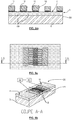
- the representation of the figure 1 shows the case of an inter-electrode gap modification G between the units 20, the other parameters being identical (same width W for the electrodes 11, 12, 21, 22 and two electrodes per set of electrodes).
- the units 20 are here separate structures.
- figure 2 with a plurality of units 20 each having a set of electrodes connected to a pad 1 as the three grouped units here have different inter-electrode distances so as to measure the object over several distances.
- This is particularly suitable for organic inspired nano-objects, heterogeneous as a protein with several functions along its length.
- several units 20 are juxtaposed so as to register continuity in a preferred direction which may be that of the width of the electrodes.
- the units 20 are in a row following a preferred direction of placement of an object, but also benefits from pooling a connection to the unit of measure, by sets of electrodes placed in series, games of opposing electrodes remaining separately connected to the measuring unit.
- at least a portion of the measurement units 20 are arranged in series, with respectively one set of electrodes connected to the same pad and the other sets of electrodes connected to separate pads.
- the measurement conditions are close (such as quasi-simultaneity, humidity, pressure, brightness) all on the same material.
- This design can be used for proteins of great length 100nm or to a complex object formed of several elementary objects (such as grouped nano-objects). With a high number of electrodes m, one can characterize many sections of the object and derive an average value.
- the number of measurement units 20 is not limited according to the invention. Multiply them makes it possible to carry out measurements in parallel on several objects of a same type (same material, same form in particular). This is illustrated by figure 3 with ten units. Four of them are similar to those of the figure 1 , for a measure of a first type of object. Six others are in the mode of figure 2 , with multiple parameters, applied to another type of object.
- This structure makes it possible to characterize an organic object inspired over distances of 3.76 ⁇ m and 0.86 ⁇ m taking into account a contact resistance of electrodes of width 1.99 ⁇ m using the design of the figure 1 .
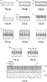
- FIG. 5a to 5h show an example.
- the height of the electrodes will be adjusted according to the object to be characterized and the object / support contact resistance constraints.
- the electrode height will preferably be between 10 nm and several tens of micrometers. Typically, the height will be 200 nm but may vary for example between 10 nm and 100 microns.
- the figure 5a has a plate of semiconductor material, such as silicon, which can form the starting substrate 50 of the manufacturing process. It comprises a first face 51 by which a unit of measure will be manufactured, and an opposite face which will form the second face 5 of the device.
- semiconductor material such as silicon
- An optional step presented in figure 5b consists in forming a oxide layer 52, in particular silicon, around the substrate 50, to protect the surfaces during a subsequent step, also optional, ion implantation.
- the oxidation is for example resulting from a heat treatment such as annealing in an oxygen atmosphere or be operated by deposition.
- the implantation is shown schematically in zone 53 figure 5c . It can allow a more efficient contact with the rear face 5. It can be carried out by p-type doping or n, for example with dopant concentrations between 10 16 to 10 20 at / cm 3 followed by annealing. activation.
- the oxide layer 52 from the figure 5b may be withdrawn, at least in part, as in figure 5d . Engraving, dry or wet, may be suitable. This step is also optional.
- the electrically conductive material (s) that will serve to form the electrode sets and any other associated conductive part are deposited after placement of an insulating layer 54 (such as SiO 2 ) if the substrate is conductive.
- the layer 54 may be epitaxially or deposited in particular by a conventional vapor phase deposition technique, typically from a few nanometers to several microns. SiH 4 can also be used.
- a tie layer 55 is preferably deposited for making the conductive layer.
- a titanium layer deposited by the PVD (Physical Vapor Deposition) or electrolysis technique can be used.
- the thickness of the layer will for example be of the order of a few nanometers to several microns thick but typically a 10 nm layer of titanium is sufficient.
- the conductive layer 56 is deposited by various techniques well known to those skilled in the art, typically by PVD, electrolysis or evaporation.
- the materials used may be platinum, gold but preferably a multi-layer will be used, one of which is composed of Ruthenium.
- the thicknesses will be of the order of a few nanometers to a few microns.
- two layers composed of gold of 200 nm and then a layer of ruthenium of 50 nm will be deposited. Ruthenium makes it possible to obtain flanks perfectly straight and thus to reduce the spacing between two electrodes, because of the anisotropy of its etching.
- mask patterns 57 are produced in order to obtain electrodes of very small widths (for example 100 nm to 10 ⁇ m but typically 1 ⁇ m).
- the height of the electrodes will be adjusted according to the nano object or other object to be characterized and the contact resistance constraints of the object or the support.
- the electrode height will be between 10 nm and several tens of micrometers. Typically, the height will be 200 nm.
- an insulating layer 58 may be deposited with at least the height of the electrodes.
- This layer will be deposited by conventional techniques such as PECVD (plasma enhanced chemical vapor deposition), LPCVD (low pressure chemical vapor deposition) and other techniques well known to those skilled in the art.
- PECVD plasma enhanced chemical vapor deposition
- LPCVD low pressure chemical vapor deposition
- a silicon oxide layer will be deposited on a silicon substrate by PECVD with a height at least equal to the height of the electrodes.
- the oxide thickness between the electrodes will be at least 200 nm equivalent to the height of the electrodes of 200 nm. This is visible in figure 5j .
- an insulating layer 58 may be present on the electrodes.
- a partial polishing removal step such as Chemical Mechanical Polishing (CMP) or dry and / or wet etching will be performed to expose the electrodes.
- CMP Chemical Mechanical Polishing
- a removal of 300 nm of oxide will be carried out. The result is visible in figure 5k .
- the conductive layer 58 may be in several sub-layers of different materials.
- FIG. figure 5k shows electrodes flush with the first face 4 of the device thus constructed. Similarly, inter-electrode non-conductive portions 59 are flush with the first face 4. This provides a planar contact for the object to be measured, as is apparent from FIG. figure 5l .
- the non-conductive portions 59 are at a lower height level than the electrodes 11, 12 so that the object 10, particularly if it is filiform such a filiform protein, is deformed according to the thickness of the substrate, and not not in the plane of the upper face of the electrodes 11, 12. This case is generally less favorable than that of the figure 5l .
- the embodiment flush of the electrodes 11, 12 relative to the non-conductive portions, so that the assembly is in the plane of the face of the support 3 is preferred. This characteristic of forming the electrodes 11, 12 flush can also be implemented independently of other aspects of the invention, for example those related to the differential measurement with several units of measurement.
- the invention also relates to a device for measuring an electrical characteristic of an object comprising at least one measuring unit, with two sets of electrodes whose upper surface is flush with respect to the part of the face of the support. which surrounds the electrodes, including conductive inter-electrode portions.
- the measurement circuit typically comprises a power supply source 30 and at least one measuring system 40 of electrical quantities, in particular currents, these elements being fixedly connected or not to the electrodes, preferably via pins 1, 2a. , 2b, 2c (not visible in figure 6b ). It is thus possible, with a measurement of the current at the terminals of the studs 1, 2a, 2b, 2c, to evaluate the electrical contribution of the object to the currents measured, advantageously taking account of parasitic currents.
- the currents are often low for nano-objects, for example between 5-10 -9 A and 5 ⁇ 10 -8 A for an amyloid protein.
- At least one object is placed on a unit of measurement, arranging so that it has a transverse orientation to the length of the electrodes.
- the placement can take place by depositing drops of solution in which the object or objects to be characterized are present.
- the device itself may also be immersed, at least by one face where units of measurement are located, in a solution containing the objects.
- the presence of multiple units of measurement increases the likelihood of good positioning of the objects on the units.
- the objects placed on the units are identical (in particular same material and same dimensions) simultaneous measurements are possible.
Landscapes
- Chemical & Material Sciences (AREA)
- Health & Medical Sciences (AREA)
- Life Sciences & Earth Sciences (AREA)
- Physics & Mathematics (AREA)
- Engineering & Computer Science (AREA)
- Biochemistry (AREA)
- Immunology (AREA)
- Pathology (AREA)
- General Physics & Mathematics (AREA)
- General Health & Medical Sciences (AREA)
- Analytical Chemistry (AREA)
- Biomedical Technology (AREA)
- Chemical Kinetics & Catalysis (AREA)
- Electrochemistry (AREA)
- Urology & Nephrology (AREA)
- Food Science & Technology (AREA)
- Medicinal Chemistry (AREA)
- Molecular Biology (AREA)
- Nanotechnology (AREA)
- Hematology (AREA)
- Biophysics (AREA)
- Spectroscopy & Molecular Physics (AREA)
- Investigating Or Analyzing Materials By The Use Of Electric Means (AREA)
Claims (16)
- Elektronische Vorrichtung zum Messen mindestens eines elektrischen Parameters eines bestimmten Typs eines Gegenstands (10), umfassend:- einen Träger (3), der mit mindestens zwei Messeinheiten (20) versehen ist, wobei jede mindestens zwei Elektrodensätze Ji umfasst mit i als ganzer Zahl größer oder gleich 2, jeder Elektrodensatz (Ji) eine Anzahl mi von Elektroden umfasst, die größer oder gleich eins ist, die Elektroden eines Elektrodensatzes Ji eine Breitenabmessung (WJi) aufweisen, die Elektroden der Elektrodensätze einer selben Messeinheit (20) so ineinandergreifen, dass jede Elektrode des einen der Elektrodensätze Ji der Messeinheit (20) mit einem interelektrodischen Abstand (G(JiJi+1)) von einer Elektrode des anderen der Elektrodensätze Ji+1 der Messeinheit (20) angeordnet ist, die an diese angrenzt; wobei die Elektroden der Elektrodensätze einer Messeinheit für diese Messeinheit (20) eine Aufnahmezone (ZJ1J2) für mindestens einen Gegenstand (10) des bestimmten Typs bilden, in dieser Aufnahmezone eine diskontinuierliche Kontaktierzone mit den Elektroden der Messeinheit definiert wird, die geeignet ist, mit einem Gegenstand (10) des bestimmten Typs in Kontakt gebracht zu werden, die Kontaktierzone eine Länge aufweist, die gemäß der Breitenabmessung (W) der Elektroden entsprechend der Summe der Breiten (WJi) der Elektroden bestimmt wird, und jede Aufnahmezone ferner eine diskontinuierliche interelektrodische Zone umfasst, die eine Länge aufweist, die gemäß der Breitenabmessung (W) der Elektroden der Messeinheit (20) vorgegeben wird;- eine Messschaltung, die mit den Elektrodensätzen jeder Messeinheit verbunden ist, um für jede Messeinheit einen durch den Gegenstand fließenden Stromwert zu bestimmen;wobei sich in der Vorrichtung mindestens zwei Messeinheiten (20) untereinander hinsichtlich der Länge ihrer Kontaktierzonen und/oder der Länge ihrer interelektrodischen Zonen unterscheiden, wobei die Messschaltung dazu ausgelegt ist, einen Unterschied der Stromwerte der mindestens zwei Messeinheiten (20) zu bestimmen und einen Differenzwert des elektrischen Kontaktwiderstands zwischen einem Gegenstand des bestimmten Typs und den Elektroden einer jeden Messeinheit (20) zu bestimmen.
- Vorrichtung nach dem vorangehenden Anspruch, bei der für zumindest eine Messeinheit (20) zumindest ein Elektrodensatz (Ji) eine Anzahl mi von Elektroden umfasst, die größer oder gleich 2 ist.
- Vorrichtung nach einem der vorangehenden Ansprüche, bei der jede Messeinheit (20) eine Breitenabmessung aufweist, die kleiner oder gleich der Längenabmessung des bestimmten Gegenstandstyps ist.
- Vorrichtung nach einem der vorangehenden Ansprüche, umfassend mindestens zwei Messeinheiten, die gemäß der Breitenabmessung (W) nebeneinander angeordnet sind.
- Vorrichtung nach einem der vorangehenden Ansprüche, bei der in jedem Elektrodensatz einer jeden Messeinheit (20) die Breitenabmessung (W) der Elektroden identisch ist und bei der sich die Länge der Kontaktierzone von mindestens zwei Messeinheiten durch die Breite (W) der Elektroden von mindestens einem Elektrodensatz einer jeden der mindestens zwei Messeinheiten (20) unterscheidet.
- Vorrichtung nach einem der vorangehenden Ansprüche, bei der sich die Länge der Kontaktierzone von mindestens zwei Messeinheiten (20) durch die Anzahl (m) der Elektroden ihrer Elektrodensätze unterscheidet.
- Vorrichtung nach einem der vorangehenden Ansprüche, bei der in jedem Elektrodensatz einer jeden Messeinheit (20) der interelektrodische Abstand identisch ist und bei der sich die Längen der interelektrodischen Zonen von mindestens zwei Messeinheiten (20) durch ihren interelektrodischen Abstand unterscheiden.
- Vorrichtung nach einem der vorangehenden Ansprüche, bei der die Messschaltung Kontaktstücke (1, 2a, 2b, 2c) aufweist, wobei die Elektrodensätze einer selben Messeinheit (20) mit verschiedenen Kontaktstücken (1, 2a, 2b, 2c) verbunden sind und bei der in der Messschaltung mindestens ein Kontaktstück (1) vorhanden ist, das mit mehreren Elektrodensätzen verbunden ist, die jeweils zu einer unterschiedlichen Messeinheit (20) gehören.
- Vorrichtung nach dem vorangehenden Anspruch, bei der mindestens ein Kontaktstück auf einer Seite des Trägers (3) vorgesehen ist, die sich von einer Seite (4) unterscheidet, auf der die Messeinheit (20) vorgesehen ist, mit der das mindestens eine Kontaktstück (1, 2a, 2b, 2c) verbunden ist, und bei der die Messschaltung einen Verbindungsabschnitt zu dem mindestens einen Kontaktstück (1, 2a, 2b, 2c) der Messeinheit (20) umfasst, vorzugsweise den Träger durchquerend.
- Vorrichtung nach einem der vorangehenden Ansprüche, bei der die Elektroden der Elektrodensätze von mindestens einer Messeinheit bündig auf einer Seite des Trägers (3) sind und bei der die Elektroden der Elektrodensätze der mindestens einen Messeinheit (20) durch nichtleitende Abschnitte beabstandet sind, die bündig auf der Seite (4) des Trägers (3) sind.
- Vorrichtung nach einem der vorangehenden Ansprüche, bei der die Breitenabmessung (W) der Elektroden geringer als 1 µm ist und/oder der interelektrodische Abstand zwischen 500 nm und 1 µm beträgt.
- Vorrichtung nach einem der vorangehenden Ansprüche, bei der der Träger (3) eine erste Seite, die mit mindestens einer Messeinheit (20) versehen ist, und eine von der ersten Seite verschiedene zweite Seite aufweist, die mit mindestens einer Messeinheit (20) versehen ist.
- System, umfassend mindestens einen Gegenstand eines bestimmten Typs und eine Vorrichtung nach einem der vorangehenden Ansprüche, wobei mindestens zwei Messeinheiten (20) in ihren jeweiligen Aufnahmezonen einen Gegenstand empfangen.
- Verfahren zum Messen mindestens eines elektrischen Parameters eines Gegenstands, umfassend:- die Verwendung einer Vorrichtung nach einem der Ansprüche 1 bis 12;- einen Schritt des Anordnens eines Gegenstands (10) eines bestimmten Typs auf der Aufnahmezone einer Messeinheit (20) und einen Schritt des Messens des zwischen den Elektrodensätzen der Einheit (20) fließenden Stroms;- einen Schritt des Anordnens des Gegenstands (10) oder eines Gegenstands vom bestimmten Typ auf der Aufnahmezone einer anderen Messeinheit (20) und einen Schritt des Messens des zwischen den Elektrodensätzen der anderen Einheit (20) fließenden Stroms;- eine Bestimmung einer Differenz der Stromwerte der Messeinheiten (20) und eine Bestimmung eines Differenzwertes des elektrischen Kontaktwiderstands zwischen einem Gegenstand vom bestimmten Typ und den Elektroden einer jeden der Messeinheiten (20);- eine Bewertung des den Gegenstand durchfließenden Stroms anhand der in den vorangehenden Schritten ausgeführten Messungen des Stroms.
- Verfahren nach dem vorangehenden Anspruch, bei dem der Typ des Gegenstands in einem festen Zustand besteht.
- Verfahren nach einem der zwei vorangehenden Ansprüche, bei dem eine Vorrichtung verwendet wird, die mindestens zwei Messeinheiten umfasst, die gemäß der Breitenabmessung (W) nebeneinander angeordnet sind, und ein Gegenstand vom bestimmten Typ gleichzeitig auf den mindestens zwei nebeneinander angeordneten Messeinheiten angeordnet wird.
Applications Claiming Priority (1)
| Application Number | Priority Date | Filing Date | Title |
|---|---|---|---|
| FR1553533A FR3035220A1 (fr) | 2015-04-20 | 2015-04-20 | " dispositif electronique de mesure d'au moins une caracteristique electrique d'un objet " |
Publications (2)
| Publication Number | Publication Date |
|---|---|
| EP3086112A1 EP3086112A1 (de) | 2016-10-26 |
| EP3086112B1 true EP3086112B1 (de) | 2018-01-31 |
Family
ID=54329597
Family Applications (1)
| Application Number | Title | Priority Date | Filing Date |
|---|---|---|---|
| EP16165876.0A Not-in-force EP3086112B1 (de) | 2015-04-20 | 2016-04-18 | Elektronische vorrichtung zum messen mindestens eines elektrischen parameters eines gegenstands |
Country Status (3)
| Country | Link |
|---|---|
| US (1) | US10107772B2 (de) |
| EP (1) | EP3086112B1 (de) |
| FR (1) | FR3035220A1 (de) |
Families Citing this family (18)
| Publication number | Priority date | Publication date | Assignee | Title |
|---|---|---|---|---|
| CA3050062A1 (en) | 2016-01-14 | 2017-07-20 | Roswell Biotechnologies, Inc. | Molecular sensors and related methods |
| JP7280590B2 (ja) | 2016-01-28 | 2023-05-24 | ロズウェル バイオテクノロジーズ,インコーポレイテッド | 大スケールの分子電子工学センサアレイを使用する被分析物を測定するための方法および装置 |
| EP3408219B1 (de) | 2016-01-28 | 2022-08-17 | Roswell Biotechnologies, Inc | Massiv parallele dna-sequenzierungsvorrichtung |
| US10737263B2 (en) | 2016-02-09 | 2020-08-11 | Roswell Biotechnologies, Inc. | Electronic label-free DNA and genome sequencing |
| US10597767B2 (en) | 2016-02-22 | 2020-03-24 | Roswell Biotechnologies, Inc. | Nanoparticle fabrication |
| US9829456B1 (en) | 2016-07-26 | 2017-11-28 | Roswell Biotechnologies, Inc. | Method of making a multi-electrode structure usable in molecular sensing devices |
| WO2018132457A1 (en) | 2017-01-10 | 2018-07-19 | Roswell Biotechnologies, Inc. | Methods and systems for dna data storage |
| CN110520517A (zh) | 2017-01-19 | 2019-11-29 | 罗斯威尔生命技术公司 | 包括二维层材料的固态测序装置 |
| KR102879682B1 (ko) | 2017-04-25 | 2025-10-30 | 로스웰 엠이 아이엔씨. | 분자 센서들을 위한 효소 회로들 |
| US10508296B2 (en) | 2017-04-25 | 2019-12-17 | Roswell Biotechnologies, Inc. | Enzymatic circuits for molecular sensors |
| CA3057155A1 (en) | 2017-05-09 | 2018-11-15 | Roswell Biotechnologies, Inc. | Binding probe circuits for molecular sensors |
| EP3676389A4 (de) | 2017-08-30 | 2021-06-02 | Roswell Biotechnologies, Inc | Prozessive enzymatische molekulare elektronische sensoren zur speicherung von dna-daten |
| EP3694990A4 (de) | 2017-10-10 | 2022-06-15 | Roswell Biotechnologies, Inc. | Verfahren, vorrichtung und systeme zur amplikationsfreien dna-datenspeicherung |
| GB2568292B (en) * | 2017-11-11 | 2020-01-22 | Zedsen Ltd | Examining electrical properties of objects |
| CN113994013A (zh) | 2019-04-12 | 2022-01-28 | 罗斯威尔生命技术公司 | 用于分子电子学传感器的多环芳族桥 |
| WO2021045900A1 (en) | 2019-09-06 | 2021-03-11 | Roswell Biotechnologies, Inc. | Methods of fabricating nanoscale structures usable in molecular sensors and other devices |
| FR3124258B1 (fr) * | 2021-06-22 | 2023-07-14 | Withings | Dispositif de mesure électronique avec électrode |
| FR3156201A1 (fr) * | 2023-12-01 | 2025-06-06 | Commissariat à l'Energie Atomique et aux Energies Alternatives | Dispositif pour déterminer une conductivité ionique et une résistance au transport de dioxygène et de dihydrogène d’un film de polymère conducteur ionique |
Family Cites Families (8)
| Publication number | Priority date | Publication date | Assignee | Title |
|---|---|---|---|---|
| DE29501233U1 (de) * | 1995-01-27 | 1995-04-27 | SIBET GmbH (SICAN Forschungs- und Entwicklungsbetriebsgesellschaft), 30419 Hannover | Selbstüberwachungsfähiger Halbleitersensor für agressive Stoffe |
| US6557393B1 (en) * | 2000-11-22 | 2003-05-06 | Panametrics, Inc. | Thin film ppb oxygen sensor |
| CA2529300C (en) * | 2003-06-20 | 2011-10-18 | F.Hoffmann-La Roche Ag | Devices and methods relating to electrochemical biosensors |
| DE102009058260A1 (de) * | 2009-12-14 | 2011-06-16 | Continental Automotive Gmbh | Rußsensor |
| JP2011232065A (ja) * | 2010-04-26 | 2011-11-17 | Denso Corp | ガスセンサ |
| DE102011077875A1 (de) * | 2011-06-21 | 2012-12-27 | Robert Bosch Gmbh | Flüssigkeitsbehälter mit Verunreinigungssensor |
| WO2013039468A1 (en) * | 2011-09-12 | 2013-03-21 | Hewlett-Packard Development Company, L.P. | Configurable sensor arrays |
| EP2833129B1 (de) * | 2013-07-30 | 2019-10-09 | Sensirion AG | Verfahren und Vorrichtung zur Analyse von Gasen durch einen auf Leitfähigkeit basierenden Partikulat-Metalloxid-Gassensor |
-
2015
- 2015-04-20 FR FR1553533A patent/FR3035220A1/fr not_active Withdrawn
-
2016
- 2016-04-18 EP EP16165876.0A patent/EP3086112B1/de not_active Not-in-force
- 2016-04-19 US US15/132,463 patent/US10107772B2/en active Active
Non-Patent Citations (1)
| Title |
|---|
| None * |
Also Published As
| Publication number | Publication date |
|---|---|
| US20160377564A1 (en) | 2016-12-29 |
| US10107772B2 (en) | 2018-10-23 |
| FR3035220A1 (fr) | 2016-10-21 |
| EP3086112A1 (de) | 2016-10-26 |
Similar Documents
| Publication | Publication Date | Title |
|---|---|---|
| EP3086112B1 (de) | Elektronische vorrichtung zum messen mindestens eines elektrischen parameters eines gegenstands | |
| EP0267069B1 (de) | Verfahren zur Herstellung eines Dehnungsmessstreifens mit Piezowiderstand, sowie eines Beschleunigungsmessers mit einem solchen Dehnungsmessstreifen | |
| FR2951014A1 (fr) | Structure d'actionnement piezoelectrique comportant une jauge de contrainte piezoresistive integree et son procede de realisation | |
| EP2963695A2 (de) | Elektrische mehrschichtenvorrichtung | |
| FR2994019A1 (fr) | Procede pour la realisation d'une capacite | |
| EP3424875B1 (de) | Sensorvorrichtung auf der basis von nanodrähten mit zunehmender länge | |
| EP2772943B1 (de) | Herstellungsverfahren einer mikroelektronischen Vorrichtung und entsprechende Vorrichtung | |
| EP2680287B1 (de) | Anordnung für Superkondensatorvorrichtung, Superkondensatorvorrichtung, die eine solche Anordnung umfasst, und Herstellungsverfahren einer solchen Anordnung | |
| EP4635278A1 (de) | Halbleiterbauelement mit einem kapazitiven stapel und einer säule und verfahren zur herstellung davon | |
| FR2860594A1 (fr) | Magnetometre a circuit magnetique ouvert et son procede de realisation. | |
| KR102267328B1 (ko) | 프로브 니들을 제조하는 방법 및 이에 의해 제조되는 프로브 니들 | |
| EP2093797B1 (de) | Ausrichtungsverfahren von zwei Substraten mit Hilfe von Mikrospulen | |
| CH701487B1 (fr) | Structure de plots de connexion pour composant électronique. | |
| WO2015082844A1 (fr) | Systeme de determination de la forme au moins partielle d'un objet tridimentionnel et procede correspondant | |
| EP3675160A1 (de) | Gesicherte integrierte schaltung und verfahren zu ihrer herstellung | |
| EP3611660A1 (de) | Erzeugungsverfahren einer pixelmatrix eines thermischen mustersensors, und entsprechender sensor | |
| FR3011363A1 (fr) | Circuit neuromimetrique et procede de fabrication | |
| EP4256327B1 (de) | Nanostrukturplattform für zellulare schnittstelle und entsprechendes herstellungsverfahren | |
| EP4056529B1 (de) | Verfahren zum ätzen eines lochs und verfahren zur herstellung einer mikronadel unter verwendung eines solchen lochs | |
| EP3985438B1 (de) | Verfahren zur herstellung einer elektronischen baugruppe auf der vorderseite eines halbleitersubstrats | |
| WO2006040500A2 (fr) | Procede de realisation d'heterostructures resonnantes a transport planaire | |
| EP4484932A1 (de) | Fluoreszenznachweisvorrichtung mit nanofotodetektoren | |
| EP4482286A1 (de) | Elektronische vorrichtung mit einer schicht aus 2d-material | |
| EP4484933A1 (de) | Fluoreszenznachweisvorrichtung mit nanofotodetektoren | |
| FR3117101A1 (fr) | Plateforme de nanostructures pour l’interfaçage cellulaire et procédé de fabrication correspondant |
Legal Events
| Date | Code | Title | Description |
|---|---|---|---|
| PUAI | Public reference made under article 153(3) epc to a published international application that has entered the european phase |
Free format text: ORIGINAL CODE: 0009012 |
|
| 17P | Request for examination filed |
Effective date: 20160418 |
|
| AK | Designated contracting states |
Kind code of ref document: A1 Designated state(s): AL AT BE BG CH CY CZ DE DK EE ES FI FR GB GR HR HU IE IS IT LI LT LU LV MC MK MT NL NO PL PT RO RS SE SI SK SM TR |
|
| AX | Request for extension of the european patent |
Extension state: BA ME |
|
| GRAP | Despatch of communication of intention to grant a patent |
Free format text: ORIGINAL CODE: EPIDOSNIGR1 |
|
| STAA | Information on the status of an ep patent application or granted ep patent |
Free format text: STATUS: GRANT OF PATENT IS INTENDED |
|
| RIC1 | Information provided on ipc code assigned before grant |
Ipc: G01N 27/12 20060101AFI20170627BHEP Ipc: G01N 33/487 20060101ALI20170627BHEP |
|
| INTG | Intention to grant announced |
Effective date: 20170714 |
|
| GRAS | Grant fee paid |
Free format text: ORIGINAL CODE: EPIDOSNIGR3 |
|
| GRAJ | Information related to disapproval of communication of intention to grant by the applicant or resumption of examination proceedings by the epo deleted |
Free format text: ORIGINAL CODE: EPIDOSDIGR1 |
|
| GRAL | Information related to payment of fee for publishing/printing deleted |
Free format text: ORIGINAL CODE: EPIDOSDIGR3 |
|
| STAA | Information on the status of an ep patent application or granted ep patent |
Free format text: STATUS: REQUEST FOR EXAMINATION WAS MADE |
|
| GRAR | Information related to intention to grant a patent recorded |
Free format text: ORIGINAL CODE: EPIDOSNIGR71 |
|
| STAA | Information on the status of an ep patent application or granted ep patent |
Free format text: STATUS: GRANT OF PATENT IS INTENDED |
|
| INTC | Intention to grant announced (deleted) | ||
| GRAA | (expected) grant |
Free format text: ORIGINAL CODE: 0009210 |
|
| STAA | Information on the status of an ep patent application or granted ep patent |
Free format text: STATUS: THE PATENT HAS BEEN GRANTED |
|
| INTG | Intention to grant announced |
Effective date: 20171218 |
|
| AK | Designated contracting states |
Kind code of ref document: B1 Designated state(s): AL AT BE BG CH CY CZ DE DK EE ES FI FR GB GR HR HU IE IS IT LI LT LU LV MC MK MT NL NO PL PT RO RS SE SI SK SM TR |
|
| REG | Reference to a national code |
Ref country code: GB Ref legal event code: FG4D Free format text: NOT ENGLISH Ref country code: CH Ref legal event code: EP |
|
| REG | Reference to a national code |
Ref country code: AT Ref legal event code: REF Ref document number: 967843 Country of ref document: AT Kind code of ref document: T Effective date: 20180215 |
|
| REG | Reference to a national code |
Ref country code: IE Ref legal event code: FG4D Free format text: LANGUAGE OF EP DOCUMENT: FRENCH |
|
| REG | Reference to a national code |
Ref country code: DE Ref legal event code: R096 Ref document number: 602016001501 Country of ref document: DE |
|
| REG | Reference to a national code |
Ref country code: FR Ref legal event code: PLFP Year of fee payment: 3 |
|
| REG | Reference to a national code |
Ref country code: NL Ref legal event code: MP Effective date: 20180131 |
|
| REG | Reference to a national code |
Ref country code: LT Ref legal event code: MG4D |
|
| REG | Reference to a national code |
Ref country code: AT Ref legal event code: MK05 Ref document number: 967843 Country of ref document: AT Kind code of ref document: T Effective date: 20180131 |
|
| PG25 | Lapsed in a contracting state [announced via postgrant information from national office to epo] |
Ref country code: LT Free format text: LAPSE BECAUSE OF FAILURE TO SUBMIT A TRANSLATION OF THE DESCRIPTION OR TO PAY THE FEE WITHIN THE PRESCRIBED TIME-LIMIT Effective date: 20180131 Ref country code: HR Free format text: LAPSE BECAUSE OF FAILURE TO SUBMIT A TRANSLATION OF THE DESCRIPTION OR TO PAY THE FEE WITHIN THE PRESCRIBED TIME-LIMIT Effective date: 20180131 Ref country code: NL Free format text: LAPSE BECAUSE OF FAILURE TO SUBMIT A TRANSLATION OF THE DESCRIPTION OR TO PAY THE FEE WITHIN THE PRESCRIBED TIME-LIMIT Effective date: 20180131 Ref country code: FI Free format text: LAPSE BECAUSE OF FAILURE TO SUBMIT A TRANSLATION OF THE DESCRIPTION OR TO PAY THE FEE WITHIN THE PRESCRIBED TIME-LIMIT Effective date: 20180131 Ref country code: NO Free format text: LAPSE BECAUSE OF FAILURE TO SUBMIT A TRANSLATION OF THE DESCRIPTION OR TO PAY THE FEE WITHIN THE PRESCRIBED TIME-LIMIT Effective date: 20180430 Ref country code: ES Free format text: LAPSE BECAUSE OF FAILURE TO SUBMIT A TRANSLATION OF THE DESCRIPTION OR TO PAY THE FEE WITHIN THE PRESCRIBED TIME-LIMIT Effective date: 20180131 |
|
| PG25 | Lapsed in a contracting state [announced via postgrant information from national office to epo] |
Ref country code: AT Free format text: LAPSE BECAUSE OF FAILURE TO SUBMIT A TRANSLATION OF THE DESCRIPTION OR TO PAY THE FEE WITHIN THE PRESCRIBED TIME-LIMIT Effective date: 20180131 Ref country code: RS Free format text: LAPSE BECAUSE OF FAILURE TO SUBMIT A TRANSLATION OF THE DESCRIPTION OR TO PAY THE FEE WITHIN THE PRESCRIBED TIME-LIMIT Effective date: 20180131 Ref country code: LV Free format text: LAPSE BECAUSE OF FAILURE TO SUBMIT A TRANSLATION OF THE DESCRIPTION OR TO PAY THE FEE WITHIN THE PRESCRIBED TIME-LIMIT Effective date: 20180131 Ref country code: GR Free format text: LAPSE BECAUSE OF FAILURE TO SUBMIT A TRANSLATION OF THE DESCRIPTION OR TO PAY THE FEE WITHIN THE PRESCRIBED TIME-LIMIT Effective date: 20180501 Ref country code: SE Free format text: LAPSE BECAUSE OF FAILURE TO SUBMIT A TRANSLATION OF THE DESCRIPTION OR TO PAY THE FEE WITHIN THE PRESCRIBED TIME-LIMIT Effective date: 20180131 Ref country code: IS Free format text: LAPSE BECAUSE OF FAILURE TO SUBMIT A TRANSLATION OF THE DESCRIPTION OR TO PAY THE FEE WITHIN THE PRESCRIBED TIME-LIMIT Effective date: 20180531 Ref country code: BG Free format text: LAPSE BECAUSE OF FAILURE TO SUBMIT A TRANSLATION OF THE DESCRIPTION OR TO PAY THE FEE WITHIN THE PRESCRIBED TIME-LIMIT Effective date: 20180430 Ref country code: PL Free format text: LAPSE BECAUSE OF FAILURE TO SUBMIT A TRANSLATION OF THE DESCRIPTION OR TO PAY THE FEE WITHIN THE PRESCRIBED TIME-LIMIT Effective date: 20180131 |
|
| PG25 | Lapsed in a contracting state [announced via postgrant information from national office to epo] |
Ref country code: MT Free format text: LAPSE BECAUSE OF FAILURE TO SUBMIT A TRANSLATION OF THE DESCRIPTION OR TO PAY THE FEE WITHIN THE PRESCRIBED TIME-LIMIT Effective date: 20180131 |
|
| PG25 | Lapsed in a contracting state [announced via postgrant information from national office to epo] |
Ref country code: RO Free format text: LAPSE BECAUSE OF FAILURE TO SUBMIT A TRANSLATION OF THE DESCRIPTION OR TO PAY THE FEE WITHIN THE PRESCRIBED TIME-LIMIT Effective date: 20180131 Ref country code: EE Free format text: LAPSE BECAUSE OF FAILURE TO SUBMIT A TRANSLATION OF THE DESCRIPTION OR TO PAY THE FEE WITHIN THE PRESCRIBED TIME-LIMIT Effective date: 20180131 Ref country code: IT Free format text: LAPSE BECAUSE OF FAILURE TO SUBMIT A TRANSLATION OF THE DESCRIPTION OR TO PAY THE FEE WITHIN THE PRESCRIBED TIME-LIMIT Effective date: 20180131 Ref country code: AL Free format text: LAPSE BECAUSE OF FAILURE TO SUBMIT A TRANSLATION OF THE DESCRIPTION OR TO PAY THE FEE WITHIN THE PRESCRIBED TIME-LIMIT Effective date: 20180131 |
|
| REG | Reference to a national code |
Ref country code: DE Ref legal event code: R097 Ref document number: 602016001501 Country of ref document: DE |
|
| PG25 | Lapsed in a contracting state [announced via postgrant information from national office to epo] |
Ref country code: SK Free format text: LAPSE BECAUSE OF FAILURE TO SUBMIT A TRANSLATION OF THE DESCRIPTION OR TO PAY THE FEE WITHIN THE PRESCRIBED TIME-LIMIT Effective date: 20180131 Ref country code: SM Free format text: LAPSE BECAUSE OF FAILURE TO SUBMIT A TRANSLATION OF THE DESCRIPTION OR TO PAY THE FEE WITHIN THE PRESCRIBED TIME-LIMIT Effective date: 20180131 Ref country code: DK Free format text: LAPSE BECAUSE OF FAILURE TO SUBMIT A TRANSLATION OF THE DESCRIPTION OR TO PAY THE FEE WITHIN THE PRESCRIBED TIME-LIMIT Effective date: 20180131 Ref country code: MC Free format text: LAPSE BECAUSE OF FAILURE TO SUBMIT A TRANSLATION OF THE DESCRIPTION OR TO PAY THE FEE WITHIN THE PRESCRIBED TIME-LIMIT Effective date: 20180131 Ref country code: CZ Free format text: LAPSE BECAUSE OF FAILURE TO SUBMIT A TRANSLATION OF THE DESCRIPTION OR TO PAY THE FEE WITHIN THE PRESCRIBED TIME-LIMIT Effective date: 20180131 |
|
| PLBE | No opposition filed within time limit |
Free format text: ORIGINAL CODE: 0009261 |
|
| STAA | Information on the status of an ep patent application or granted ep patent |
Free format text: STATUS: NO OPPOSITION FILED WITHIN TIME LIMIT |
|
| REG | Reference to a national code |
Ref country code: BE Ref legal event code: MM Effective date: 20180430 |
|
| 26N | No opposition filed |
Effective date: 20181102 |
|
| REG | Reference to a national code |
Ref country code: IE Ref legal event code: MM4A |
|
| PG25 | Lapsed in a contracting state [announced via postgrant information from national office to epo] |
Ref country code: LU Free format text: LAPSE BECAUSE OF NON-PAYMENT OF DUE FEES Effective date: 20180418 |
|
| PG25 | Lapsed in a contracting state [announced via postgrant information from national office to epo] |
Ref country code: SI Free format text: LAPSE BECAUSE OF FAILURE TO SUBMIT A TRANSLATION OF THE DESCRIPTION OR TO PAY THE FEE WITHIN THE PRESCRIBED TIME-LIMIT Effective date: 20180131 Ref country code: BE Free format text: LAPSE BECAUSE OF NON-PAYMENT OF DUE FEES Effective date: 20180430 |
|
| PG25 | Lapsed in a contracting state [announced via postgrant information from national office to epo] |
Ref country code: IE Free format text: LAPSE BECAUSE OF NON-PAYMENT OF DUE FEES Effective date: 20180418 |
|
| REG | Reference to a national code |
Ref country code: CH Ref legal event code: PL |
|
| PG25 | Lapsed in a contracting state [announced via postgrant information from national office to epo] |
Ref country code: CH Free format text: LAPSE BECAUSE OF NON-PAYMENT OF DUE FEES Effective date: 20190430 Ref country code: LI Free format text: LAPSE BECAUSE OF NON-PAYMENT OF DUE FEES Effective date: 20190430 |
|
| PG25 | Lapsed in a contracting state [announced via postgrant information from national office to epo] |
Ref country code: TR Free format text: LAPSE BECAUSE OF FAILURE TO SUBMIT A TRANSLATION OF THE DESCRIPTION OR TO PAY THE FEE WITHIN THE PRESCRIBED TIME-LIMIT Effective date: 20180131 |
|
| PG25 | Lapsed in a contracting state [announced via postgrant information from national office to epo] |
Ref country code: PT Free format text: LAPSE BECAUSE OF FAILURE TO SUBMIT A TRANSLATION OF THE DESCRIPTION OR TO PAY THE FEE WITHIN THE PRESCRIBED TIME-LIMIT Effective date: 20180131 |
|
| PG25 | Lapsed in a contracting state [announced via postgrant information from national office to epo] |
Ref country code: MK Free format text: LAPSE BECAUSE OF NON-PAYMENT OF DUE FEES Effective date: 20180131 Ref country code: HU Free format text: LAPSE BECAUSE OF FAILURE TO SUBMIT A TRANSLATION OF THE DESCRIPTION OR TO PAY THE FEE WITHIN THE PRESCRIBED TIME-LIMIT; INVALID AB INITIO Effective date: 20160418 Ref country code: CY Free format text: LAPSE BECAUSE OF FAILURE TO SUBMIT A TRANSLATION OF THE DESCRIPTION OR TO PAY THE FEE WITHIN THE PRESCRIBED TIME-LIMIT Effective date: 20180131 |
|
| PGFP | Annual fee paid to national office [announced via postgrant information from national office to epo] |
Ref country code: DE Payment date: 20230418 Year of fee payment: 8 |
|
| PGFP | Annual fee paid to national office [announced via postgrant information from national office to epo] |
Ref country code: GB Payment date: 20240418 Year of fee payment: 9 |
|
| PGFP | Annual fee paid to national office [announced via postgrant information from national office to epo] |
Ref country code: FR Payment date: 20240422 Year of fee payment: 9 |
|
| REG | Reference to a national code |
Ref country code: DE Ref legal event code: R119 Ref document number: 602016001501 Country of ref document: DE |
|
| GBPC | Gb: european patent ceased through non-payment of renewal fee |
Effective date: 20250418 |
|
| PG25 | Lapsed in a contracting state [announced via postgrant information from national office to epo] |
Ref country code: DE Free format text: LAPSE BECAUSE OF NON-PAYMENT OF DUE FEES Effective date: 20251104 |
|
| PG25 | Lapsed in a contracting state [announced via postgrant information from national office to epo] |
Ref country code: GB Free format text: LAPSE BECAUSE OF NON-PAYMENT OF DUE FEES Effective date: 20250418 |
|
| PG25 | Lapsed in a contracting state [announced via postgrant information from national office to epo] |
Ref country code: FR Free format text: LAPSE BECAUSE OF NON-PAYMENT OF DUE FEES Effective date: 20250430 |