EP3080845B1 - Method and circuitry for controlling a depletion-mode transistor - Google Patents
Method and circuitry for controlling a depletion-mode transistor Download PDFInfo
- Publication number
- EP3080845B1 EP3080845B1 EP14861236.9A EP14861236A EP3080845B1 EP 3080845 B1 EP3080845 B1 EP 3080845B1 EP 14861236 A EP14861236 A EP 14861236A EP 3080845 B1 EP3080845 B1 EP 3080845B1
- Authority
- EP
- European Patent Office
- Prior art keywords
- transistor
- response
- turning
- gate
- circuitry
- Prior art date
- Legal status (The legal status is an assumption and is not a legal conclusion. Google has not performed a legal analysis and makes no representation as to the accuracy of the status listed.)
- Active
Links
- 238000000034 method Methods 0.000 title claims description 10
- 238000001514 detection method Methods 0.000 claims description 10
- 229910002601 GaN Inorganic materials 0.000 claims description 5
- JMASRVWKEDWRBT-UHFFFAOYSA-N Gallium nitride Chemical compound [Ga]#N JMASRVWKEDWRBT-UHFFFAOYSA-N 0.000 claims description 3
- 239000008186 active pharmaceutical agent Substances 0.000 description 3
- 230000005669 field effect Effects 0.000 description 3
- 238000010586 diagram Methods 0.000 description 2
- HBMJWWWQQXIZIP-UHFFFAOYSA-N silicon carbide Chemical compound [Si+]#[C-] HBMJWWWQQXIZIP-UHFFFAOYSA-N 0.000 description 2
- 229910010271 silicon carbide Inorganic materials 0.000 description 2
- 230000001419 dependent effect Effects 0.000 description 1
- 229910044991 metal oxide Inorganic materials 0.000 description 1
- 150000004706 metal oxides Chemical class 0.000 description 1
- 238000012986 modification Methods 0.000 description 1
- 230000004048 modification Effects 0.000 description 1
- 239000004065 semiconductor Substances 0.000 description 1
Images
Classifications
-
- H—ELECTRICITY
- H03—ELECTRONIC CIRCUITRY
- H03K—PULSE TECHNIQUE
- H03K17/00—Electronic switching or gating, i.e. not by contact-making and –breaking
- H03K17/08—Modifications for protecting switching circuit against overcurrent or overvoltage
- H03K17/082—Modifications for protecting switching circuit against overcurrent or overvoltage by feedback from the output to the control circuit
- H03K17/0822—Modifications for protecting switching circuit against overcurrent or overvoltage by feedback from the output to the control circuit in field-effect transistor switches
-
- H—ELECTRICITY
- H02—GENERATION; CONVERSION OR DISTRIBUTION OF ELECTRIC POWER
- H02H—EMERGENCY PROTECTIVE CIRCUIT ARRANGEMENTS
- H02H3/00—Emergency protective circuit arrangements for automatic disconnection directly responsive to an undesired change from normal electric working condition with or without subsequent reconnection ; integrated protection
-
- H—ELECTRICITY
- H03—ELECTRONIC CIRCUITRY
- H03K—PULSE TECHNIQUE
- H03K17/00—Electronic switching or gating, i.e. not by contact-making and –breaking
- H03K17/08—Modifications for protecting switching circuit against overcurrent or overvoltage
-
- H—ELECTRICITY
- H03—ELECTRONIC CIRCUITRY
- H03K—PULSE TECHNIQUE
- H03K17/00—Electronic switching or gating, i.e. not by contact-making and –breaking
- H03K17/10—Modifications for increasing the maximum permissible switched voltage
- H03K17/102—Modifications for increasing the maximum permissible switched voltage in field-effect transistor switches
-
- H—ELECTRICITY
- H03—ELECTRONIC CIRCUITRY
- H03K—PULSE TECHNIQUE
- H03K3/00—Circuits for generating electric pulses; Monostable, bistable or multistable circuits
- H03K3/01—Details
- H03K3/012—Modifications of generator to improve response time or to decrease power consumption
-
- H—ELECTRICITY
- H03—ELECTRONIC CIRCUITRY
- H03K—PULSE TECHNIQUE
- H03K17/00—Electronic switching or gating, i.e. not by contact-making and –breaking
- H03K17/08—Modifications for protecting switching circuit against overcurrent or overvoltage
- H03K2017/0806—Modifications for protecting switching circuit against overcurrent or overvoltage against excessive temperature
-
- H—ELECTRICITY
- H03—ELECTRONIC CIRCUITRY
- H03K—PULSE TECHNIQUE
- H03K17/00—Electronic switching or gating, i.e. not by contact-making and –breaking
- H03K17/51—Electronic switching or gating, i.e. not by contact-making and –breaking characterised by the components used
- H03K17/56—Electronic switching or gating, i.e. not by contact-making and –breaking characterised by the components used by the use, as active elements, of semiconductor devices
- H03K17/687—Electronic switching or gating, i.e. not by contact-making and –breaking characterised by the components used by the use, as active elements, of semiconductor devices the devices being field-effect transistors
- H03K2017/6875—Electronic switching or gating, i.e. not by contact-making and –breaking characterised by the components used by the use, as active elements, of semiconductor devices the devices being field-effect transistors using self-conductive, depletion FETs
Definitions
- This relates in general to electronic circuitry, and in particular to a method and circuitry for controlling a depletion-mode transistor.
- depletion-mode (“d-mode”) transistors such as gallium nitride (“GaN”) high-electron-mobility transistors (“HEMTs”) and silicon carbide (“SiC”) junction gate field-effect transistors (“JFETs”)
- GaN gallium nitride
- HEMTs high-electron-mobility transistors
- SiC silicon carbide
- JFETs junction gate field-effect transistors
- e-mode enhancement-mode
- a normally “off e-mode transistor may help to substantially prevent cross-conduction (such as short circuiting) in response to certain fault conditions.
- Circuits for controlling a depletion-mode transistor are known from documents DE 10 2010 046539 A1 , US 4 042 839 A and DE 10 2006 029928 B3 .
- Circuitry for controlling a depletion-mode transistor and a corresponding method according to the invention are defined in the appended independent claims. Preferred embodiments are defined in the dependent claims.
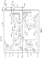
- FIG. 1 is a schematic electrical circuit diagram of circuitry of the example embodiments.
- FIG. 1 is a schematic electrical circuit diagram of circuitry 100 of the example embodiments.
- a high-voltage d-mode transistor 102 such as a GaN HEMT, is connected in series with a low-voltage e-mode NFET ("LV switch") 104.
- LV switch 104 is discrete.
- the LV switch 104 is integrated with another component (such as being integrated with driver circuitry 105).
- a drain of the d-mode transistor 102 is connected to a voltage output node VOUT whose voltage may range up to 600 volts (or beyond).
- a source of the d-mode transistor 102 is connected to a drain of the LV switch 104.
- a source of the LV switch 104 is connected to a voltage reference node, such as a ground node GND whose voltage is 0 volts. In at least one example, the ground node GND is connected to a local ground instead of a global ground.
- the LV switch 104 (a) turns on for normal operation, so that n-channel metal oxide semiconductor ("NMOS") switching dynamics are substantially removed from overall switching dynamics of the circuitry 100 during normal operation; and (b) turns off for safety (such as device protection) in response to one or more detected fault conditions (such as during startup). Examples of such fault conditions are under-voltage, over-voltage, over-current, and over-temperature.
- NMOS metal oxide semiconductor
- under-voltage lockout (“UVLO") circuitry 106 detects: (a) whether an under-voltage condition exists or is absent; and (b) whether an over-voltage condition exists or is absent. In response to such detection, the UVLO circuitry 106 outputs a signal on a PGOOD line to respective first inputs of AND gates 108 and 110. Accordingly, in response to the UVLO circuitry 106 detecting neither an under-voltage condition nor an over-voltage condition, the signal from the UVLO circuitry 106 on the PGOOD line has a binary logic 1 ("true") state. Conversely, in response to the UVLO circuitry 106 detecting either an under-voltage condition or an over-voltage condition, the signal from the UVLO circuitry 106 on the PGOOD line has a binary logic 0 ("false") state.
- UVLO under-voltage lockout
- over-current protection (“OCP”) over-temperature protection (“OTP”) circuitry 112 detects: (a) whether an over-current condition exists or is absent; and (b) whether an over-temperature condition exists or is absent. In response to such detection, the OCP OTP circuitry 112 outputs a signal on a /FAULT line to respective second inputs of the AND gates 108 and 110.
- the OCP OTP circuitry 112 and the UVLO circuitry 106 are examples of fault detection circuitry.
- An output of the AND gate 110 is coupled through a buffer 114 to a control node 115.
- the control node 115 is coupled to the gate of the LV switch 104. Accordingly, if the signal on the PGOOD line has the true state, and if the signal on the /FAULT line has the true state, then the output of the AND gate 110 has the true state, and the LV switch 104 turns on for normal operation. Conversely, if the signal on the PGOOD line has the false state, or if the signal on the /FAULT line has the false state, then the output of the AND gate 110 has the false state, and the LV switch 104 turns off for safety in response to one or more of those detected fault conditions.
- an output of the AND gate 108 is coupled through an inverter 116 to a gate of an n-channel field-effect transistor ("NFET") 118.
- NFET n-channel field-effect transistor
- a source of the NFET 118 is connected to the ground node GND, and a drain of the NFET 118 is connected to a FAULT node. Accordingly, if the signal on the PGOOD line has the true state, and if the signal on the /FAULT line has the true state, then the output of the AND gate 108 has the true state, so the NFET 118 turns off.
- the output of the AND gate 108 has the false state, thereby turning on the NFET 118.
- the FAULT node is coupled through the NFET 118 to 0 volts, which thereby communicates (via the FAULT node) existence of one or more of those detected fault conditions.
- the output of the AND gate 108 is connected to a first input of an AND gate 120.
- An input node IN is coupled through a buffer 122 to a second input of the AND gate 120.
- the input node IN receives a pulse width modulated (“PWM”) signal (such as from a PWM controller), which alternates between a binary logic 1 (“true”) state and a binary logic 0 (“false”) state.
- PWM pulse width modulated
- the logic state of the input node IN propagates through the AND gate 120, so the output of the AND gate 120 has the same logic (either true or false) state as the input node IN; and (b) conversely, if the signal on the PGOOD line has the false state, or if the signal on the /FAULT line has the false state, then the output of the AND gate 120 has the false state.
- a low-dropout (“LDO") regulator 124 In response to a 12-volt input voltage at a node ("+12 V node”), a low-dropout (“LDO") regulator 124 generates a 5-volt voltage at a node ("+5 V node”).
- the +12 V node is connected to a source of a p-channel field-effect transistor ("PFET") 126.
- An inverting buck-boost controller 128 is connected to a gate of the PFET 126 and to a gate of an NFET 130.
- a source of the NFET 130 is connected to a line 132.
- a switch node SW is connected to a drain of the PFET 126 and to a drain of the NFET 130.
- an inductor (not shown for clarity) is connected between the switch node SW and the ground node GND whose voltage is 0 volts. Accordingly, in response to signals (such as voltage signals) at a feedback node FB, the controller 128 controls switching (between on and off) of the PFET 126 and NFET 130 to regulate a voltage of -12 volts on the line 132. In another example, the controller 128 is replaced by an inverting charge pump to regulate the voltage of -12 volts on the line 132 ("-12 V node").
- a gate of the d-mode transistor 102 is connected to a drain of a PFET 134 and to a drain of an NFET 136.
- a source of the PFET 134 is connected to the ground node GND whose voltage is 0 volts, and a source of the NFET 136 is connected to the line 132 whose voltage is -12 volts.
- a body diode 138 of the PFET 134 is connected from the drain of the PFET 134 to the source of the PFET 134.
- a binary logic 0 (“false”) state is represented by -5 volts
- a binary logic 1 (“true”) state is represented by 0 volts
- an AND gate 148 and a buffer 150 a binary logic 0 (“false”) state is represented by -12 volts
- a binary logic 1 (“true”) state is represented by -7 volts.
- a level shifter (L/S) 152 (a) receives the output of the AND gate 120; and (b) converts such output to corresponding signals that are suitable for the inverters 140 and 146. Accordingly, in response to the output of the AND gate 120 having the false state, the L/S 152 outputs: (a) to an input of the inverter 140, a signal whose voltage is -5 volts; and (b) to an input of the inverter 146, a signal whose voltage is -12 volts.
- the L/S 152 outputs: (a) to the input of the inverter 140, a signal whose voltage is 0 volts; and (b) to the input of the inverter 146, a signal whose voltage is -7 volts.
- An output of the inverter 140 is connected to a first input of the OR gate 142.
- An output of the OR gate 142 is connected to an input of the buffer 144.
- An output of the buffer 144 is connected to a gate of the PFET 134.
- An output of the inverter 146 is connected to a first input of the AND gate 148.
- An output of the AND gate 148 is connected to an input of the buffer 150.
- An output of the buffer 150 is connected to a gate of the NFET 136.
- a level shifter (L/S) 154 (a) receives the output of the AND gate 148; and (b) converts such output to a corresponding signal that is suitable for the OR gate 142. Accordingly: (a) in response to the output of the AND gate 148 having the false state (-12 volts), the L/S 154 outputs (to a second input of the OR gate 142) a signal whose voltage is -5 volts; and (b) conversely, in response to the output of the AND gate 148 having the true state (-7 volts), the L/S 154 outputs (to the second input of the OR gate 142) a signal whose voltage is 0 volts.
- the level shifter (L/S) 154 (a) receives the output of the OR gate 142; and (b) converts such output to a corresponding signal that is suitable for the AND gate 148. Accordingly: (a) in response to the output of the OR gate 142 having the false state (-5 volts), the L/S 154 outputs (to a second input of the AND gate 148) a signal whose voltage is -12 volts; and (b) conversely, in response to the output of the OR gate 142 having the true state (0 volts), the L/S 154 outputs (to the second input of the AND gate 148) a signal whose voltage is -7 volts.
- the respective outputs of the inverters 140 and 146 have the same binary logic state as one another, and such logic state is latched by the respective outputs of the OR gate 142 and the AND gate 148.
- a threshold voltage (V T ) of the d-mode transistor 102 is -10 volts, so the gate of the d-mode transistor 102 operates from a negative potential relative to the source of the LV switch 104.
- the circuitry 100 is operable to actively switch the gate of the d-mode transistor 102 between 0 volts and -12 volts. Accordingly, the circuitry 100 achieves a native d-mode device's superior switching performance and maintains a controllable edge rate, while preserving a cascode arrangement's inherent normally-off capability.
- the input node IN is cleared to the false state, so the output of the AND gate 120 has the false state, thereby turning off the PFET 134 and turning on the NFET 136.
- the output of the AND gate 120 has the false state, thereby turning off the PFET 134 and turning on the NFET 136.
- the gate of the d-mode transistor 102 is coupled through the NFET 136 to the line 132 whose voltage is -12 volts, so the d-mode transistor 102 is turned off.
- the input node IN is set to the true state, so the output of the AND gate 120 has the true state (but only while the output of the AND gate 108 likewise has the true state), thereby turning on the PFET 134 and turning off the NFET 136.
- the PFET 134 By turning on the PFET 134 in that manner:
- the driver circuitry 105 If the driver circuitry 105 is unpowered, then the LV switch 104 is turned off, and the gate of the d-mode transistor 102 is coupled to near 0 volts (of the ground node GND) through the diode 138. Or, if the driver circuitry 105 has power, yet any one or more of the +12 V, +5 V or -12 V nodes is not at its suitable voltage level, then the signal from the UVLO circuitry 106 on the PGOOD line has a binary logic 0 ("false") state, so the LV switch 104 is turned off.
- V DS of the LV switch 104 increases, which eventually causes V GS of the d-mode transistor 102 to reach (and continue beyond) its threshold voltage (V T ), so the d-mode transistor 102 begins (and continues) turning off, even if the line 132 is not at its suitable voltage level of -12 volts.
Description
- This relates in general to electronic circuitry, and in particular to a method and circuitry for controlling a depletion-mode transistor.
- In many situations, depletion-mode ("d-mode") transistors, such as gallium nitride ("GaN") high-electron-mobility transistors ("HEMTs") and silicon carbide ("SiC") junction gate field-effect transistors ("JFETs"), have switching performance that is superior to enhancement-mode ("e-mode") transistors. Nevertheless, in some power electronic circuit implementations, a normally "on" d-mode transistor (e.g., whose VGS = 0V) may raise concerns about safety. By comparison, a normally "off e-mode transistor may help to substantially prevent cross-conduction (such as short circuiting) in response to certain fault conditions.
- Circuits for controlling a depletion-mode transistor are known from documents
DE 10 2010 046539 A1 ,US 4 042 839 A andDE 10 2006 029928 B3 . - Circuitry for controlling a depletion-mode transistor and a corresponding method according to the invention are defined in the appended independent claims. Preferred embodiments are defined in the dependent claims.
-
FIG. 1 is a schematic electrical circuit diagram of circuitry of the example embodiments. -
FIG. 1 is a schematic electrical circuit diagram ofcircuitry 100 of the example embodiments. As shown inFIG. 1 , a high-voltage d-mode transistor 102, such as a GaN HEMT, is connected in series with a low-voltage e-mode NFET ("LV switch") 104. In a first example, theLV switch 104 is discrete. In a second example, theLV switch 104 is integrated with another component (such as being integrated with driver circuitry 105). - A drain of the d-
mode transistor 102 is connected to a voltage output node VOUT whose voltage may range up to 600 volts (or beyond). A source of the d-mode transistor 102 is connected to a drain of theLV switch 104. A source of theLV switch 104 is connected to a voltage reference node, such as a ground node GND whose voltage is 0 volts. In at least one example, the ground node GND is connected to a local ground instead of a global ground. - The LV switch 104: (a) turns on for normal operation, so that n-channel metal oxide semiconductor ("NMOS") switching dynamics are substantially removed from overall switching dynamics of the
circuitry 100 during normal operation; and (b) turns off for safety (such as device protection) in response to one or more detected fault conditions (such as during startup). Examples of such fault conditions are under-voltage, over-voltage, over-current, and over-temperature. - For example, in response to voltages at the +12 V, +5 V and -12 V nodes, under-voltage lockout ("UVLO")
circuitry 106 detects: (a) whether an under-voltage condition exists or is absent; and (b) whether an over-voltage condition exists or is absent. In response to such detection, theUVLO circuitry 106 outputs a signal on a PGOOD line to respective first inputs ofAND gates UVLO circuitry 106 detecting neither an under-voltage condition nor an over-voltage condition, the signal from theUVLO circuitry 106 on the PGOOD line has a binary logic 1 ("true") state. Conversely, in response to theUVLO circuitry 106 detecting either an under-voltage condition or an over-voltage condition, the signal from theUVLO circuitry 106 on the PGOOD line has a binary logic 0 ("false") state. - Similarly, in response to voltages at a gate of the
LV switch 104 and at the drain of theLV switch 104, over-current protection ("OCP") over-temperature protection ("OTP")circuitry 112 detects: (a) whether an over-current condition exists or is absent; and (b) whether an over-temperature condition exists or is absent. In response to such detection, theOCP OTP circuitry 112 outputs a signal on a /FAULT line to respective second inputs of theAND gates OCP OTP circuitry 112 detecting neither an over-current condition nor an over-temperature condition, the signal from theOCP OTP circuitry 112 on the /FAULT line has a binary logic 1 ("true" = no fault) state. Conversely, in response to theOCP OTP circuitry 112 detecting either an over-current condition or an over-temperature condition, the signal from theOCP OTP circuitry 112 on the /FAULT line has a binary logic 0 ("false" = fault) state. TheOCP OTP circuitry 112 and theUVLO circuitry 106 are examples of fault detection circuitry. - An output of the
AND gate 110 is coupled through abuffer 114 to acontrol node 115. Thecontrol node 115 is coupled to the gate of theLV switch 104. Accordingly, if the signal on the PGOOD line has the true state, and if the signal on the /FAULT line has the true state, then the output of theAND gate 110 has the true state, and theLV switch 104 turns on for normal operation. Conversely, if the signal on the PGOOD line has the false state, or if the signal on the /FAULT line has the false state, then the output of theAND gate 110 has the false state, and theLV switch 104 turns off for safety in response to one or more of those detected fault conditions. - Similarly, an output of the
AND gate 108 is coupled through aninverter 116 to a gate of an n-channel field-effect transistor ("NFET") 118. A source of the NFET 118 is connected to the ground node GND, and a drain of the NFET 118 is connected to aFAULT node. Accordingly, if the signal on the PGOOD line has the true state, and if the signal on the /FAULT line has the true state, then the output of theAND gate 108 has the true state, so the NFET 118 turns off. Conversely, if the signal on the PGOOD line has the false state, or if the signal on the /FAULT line has the false state, then the output of theAND gate 108 has the false state, thereby turning on the NFET 118. By turning on theNFET 118, theFAULT node is coupled through theNFET 118 to 0 volts, which thereby communicates (via theFAULT node) existence of one or more of those detected fault conditions. - Also, the output of the
AND gate 108 is connected to a first input of anAND gate 120. An input node IN is coupled through abuffer 122 to a second input of theAND gate 120. Thus, if the input node IN has a binary logic 0 ("false") state, then an output of theAND gate 120 has the false state. - For normal operation, the input node IN receives a pulse width modulated ("PWM") signal (such as from a PWM controller), which alternates between a binary logic 1 ("true") state and a binary logic 0 ("false") state. Accordingly, during normal operation: (a) if the signal on the PGOOD line has the true state, and if the signal on the /FAULT line has the true state, then the logic state of the input node IN propagates through the
AND gate 120, so the output of theAND gate 120 has the same logic (either true or false) state as the input node IN; and (b) conversely, if the signal on the PGOOD line has the false state, or if the signal on the /FAULT line has the false state, then the output of theAND gate 120 has the false state. - In response to a 12-volt input voltage at a node ("+12 V node"), a low-dropout ("LDO")
regulator 124 generates a 5-volt voltage at a node ("+5 V node"). The +12 V node is connected to a source of a p-channel field-effect transistor ("PFET") 126. An inverting buck-boost controller 128 is connected to a gate of thePFET 126 and to a gate of an NFET 130. A source of the NFET 130 is connected to aline 132. A switch node SW is connected to a drain of thePFET 126 and to a drain of the NFET 130. In at least one example, an inductor (not shown for clarity) is connected between the switch node SW and the ground node GND whose voltage is 0 volts. Accordingly, in response to signals (such as voltage signals) at a feedback node FB, thecontroller 128 controls switching (between on and off) of thePFET 126 and NFET 130 to regulate a voltage of -12 volts on theline 132. In another example, thecontroller 128 is replaced by an inverting charge pump to regulate the voltage of -12 volts on the line 132 ("-12 V node"). - A gate of the d-
mode transistor 102 is connected to a drain of aPFET 134 and to a drain of anNFET 136. A source of thePFET 134 is connected to the ground node GND whose voltage is 0 volts, and a source of theNFET 136 is connected to theline 132 whose voltage is -12 volts. Abody diode 138 of thePFET 134 is connected from the drain of thePFET 134 to the source of thePFET 134. - For an
inverter 140, anOR gate 142 and abuffer 144, a binary logic 0 ("false") state is represented by -5 volts, and a binary logic 1 ("true") state is represented by 0 volts. For aninverter 146, anAND gate 148 and abuffer 150, a binary logic 0 ("false") state is represented by -12 volts, and a binary logic 1 ("true") state is represented by -7 volts. - A level shifter (L/S) 152: (a) receives the output of the
AND gate 120; and (b) converts such output to corresponding signals that are suitable for theinverters AND gate 120 having the false state, the L/S 152 outputs: (a) to an input of theinverter 140, a signal whose voltage is -5 volts; and (b) to an input of theinverter 146, a signal whose voltage is -12 volts. Conversely, in response to the output of theAND gate 120 having the true state, the L/S 152 outputs: (a) to the input of theinverter 140, a signal whose voltage is 0 volts; and (b) to the input of theinverter 146, a signal whose voltage is -7 volts. - An output of the
inverter 140 is connected to a first input of theOR gate 142. An output of the ORgate 142 is connected to an input of thebuffer 144. An output of thebuffer 144 is connected to a gate of thePFET 134. - An output of the
inverter 146 is connected to a first input of theAND gate 148. An output of the ANDgate 148 is connected to an input of thebuffer 150. An output of thebuffer 150 is connected to a gate of theNFET 136. - A level shifter (L/S) 154: (a) receives the output of the AND
gate 148; and (b) converts such output to a corresponding signal that is suitable for theOR gate 142. Accordingly: (a) in response to the output of the ANDgate 148 having the false state (-12 volts), the L/S 154 outputs (to a second input of the OR gate 142) a signal whose voltage is -5 volts; and (b) conversely, in response to the output of the ANDgate 148 having the true state (-7 volts), the L/S 154 outputs (to the second input of the OR gate 142) a signal whose voltage is 0 volts. - Similarly, the level shifter (L/S) 154: (a) receives the output of the
OR gate 142; and (b) converts such output to a corresponding signal that is suitable for the ANDgate 148. Accordingly: (a) in response to the output of theOR gate 142 having the false state (-5 volts), the L/S 154 outputs (to a second input of the AND gate 148) a signal whose voltage is -12 volts; and (b) conversely, in response to the output of theOR gate 142 having the true state (0 volts), the L/S 154 outputs (to the second input of the AND gate 148) a signal whose voltage is -7 volts. - In that manner, the respective outputs of the
inverters OR gate 142 and the ANDgate 148. - In at least one embodiment, a threshold voltage (VT) of the d-
mode transistor 102 is -10 volts, so the gate of the d-mode transistor 102 operates from a negative potential relative to the source of theLV switch 104. For example, during normal operation, thecircuitry 100 is operable to actively switch the gate of the d-mode transistor 102 between 0 volts and -12 volts. Accordingly, thecircuitry 100 achieves a native d-mode device's superior switching performance and maintains a controllable edge rate, while preserving a cascode arrangement's inherent normally-off capability. - For turning off the d-
mode transistor 102, the input node IN is cleared to the false state, so the output of the ANDgate 120 has the false state, thereby turning off thePFET 134 and turning on theNFET 136. Likewise, in response to one or more of the detected fault conditions (irrespective of whether the input node IN is cleared to the false state or set to the true state), the output of the ANDgate 120 has the false state, thereby turning off thePFET 134 and turning on theNFET 136. By turning on theNFET 136 in that manner, the gate of the d-mode transistor 102 is coupled through theNFET 136 to theline 132 whose voltage is -12 volts, so the d-mode transistor 102 is turned off. - For turning on the d-
mode transistor 102, the input node IN is set to the true state, so the output of the ANDgate 120 has the true state (but only while the output of the ANDgate 108 likewise has the true state), thereby turning on thePFET 134 and turning off theNFET 136. By turning on thePFET 134 in that manner: - (a) the gate of the d-
mode transistor 102 is coupled through thePFET 134 to the ground node GND (and likewise to the source of the LV switch 104) whose voltage is 0 volts, so VGS of the d-mode transistor 102 is approximately equal to (but opposite polarity from) VDS of theLV switch 104; and - (b) accordingly, if the
LV switch 104 is turned on, then VDS of theLV switch 104 is relatively small, and VGS of the d-mode transistor 102 is relatively small, so the d-mode transistor 102 is turned on. - If the
driver circuitry 105 is unpowered, then theLV switch 104 is turned off, and the gate of the d-mode transistor 102 is coupled to near 0 volts (of the ground node GND) through thediode 138. Or, if thedriver circuitry 105 has power, yet any one or more of the +12 V, +5 V or -12 V nodes is not at its suitable voltage level, then the signal from theUVLO circuitry 106 on the PGOOD line has a binary logic 0 ("false") state, so theLV switch 104 is turned off. If theLV switch 104 is turned off (such as for safety in response to one or more of the detected fault conditions), then VDS of theLV switch 104 increases, which eventually causes VGS of the d-mode transistor 102 to reach (and continue beyond) its threshold voltage (VT), so the d-mode transistor 102 begins (and continues) turning off, even if theline 132 is not at its suitable voltage level of -12 volts. - Modifications are possible in the described examples, and other examples are possible, within the scope of the claims.
Claims (14)
- Circuitry for controlling a depletion-mode transistor (102), the circuitry comprising:a first transistor (104) having: a drain couplable to a source of the depletion-mode transistor; a source coupled to a first voltage node; and a gate coupled to a control node;a second transistor (134) having: a drain couplable to a gate of the depletion-mode transistor; a source coupled to the first voltage node; and a gate coupled through at least one first logic device (142) to an input node;a third transistor (136) having: a drain couplable to the gate of the depletion-mode transistor; a source coupled to a second voltage node; and a gate coupled through at least one second logic device (148) to the input node; andfault detection circuitry (106, 112) adapted to detect a fault condition,wherein the fault condition includes at least one of: an under-voltage condition; an over-voltage condition; an over-current condition; and an over-temperature condition, andwherein a voltage of the second voltage node is for turning off the depletion-mode transistor.
- The circuitry of claim 1, for controlling a gallium nitride high-electron-mobility depletion-mode transistor.
- The circuitry of claim 1, wherein the first transistor is an enhancement-mode NFET.
- The circuitry of claim 1, wherein the second transistor is a PFET, and the third transistor is an NFET.
- The circuitry of claim 1, wherein: the at least one first logic device is adapted to turn on the second transistor in response to the input node having a first logic state, and is adapted to turn off the second transistor in response to the input node having a second logic state; and the at least one second logic device is adapted to turn off the third transistor in response to the input node having the first logic state, and is adapted to turn on the third transistor in response to the input node having the second logic state.
- The circuitry of claim 1, wherein the fault detection circuitry is coupled to the control node and is adapted to turn off the first transistor in response to existence of the fault condition, and wherein turning off the first transistor is for turning off the depletion-mode transistor.
- The circuitry of claim 1, wherein: the at least one first logic device is coupled to the fault detection circuitry, and is adapted to turn on the second transistor in response to absence of the fault condition, and is adapted to turn off the second transistor in response to existence of the fault condition; and the at least one second logic device is coupled to the fault detection circuitry, and is adapted to turn off the third transistor in response to absence of the fault condition, and is adapted to turn on the third transistor in response to existence of the fault condition.
- A method of controlling a depletion-mode transistor (102), the method comprising:in response to absence of a fault condition, turning on a first transistor (104) having: a drain coupled to a source of the depletion-mode transistor; a source coupled to a first voltage node; and a gate coupled to a control node;in response to an input node having a first logic state, turning on a second transistor (134) having: a drain coupled to a gate of the depletion-mode transistor; a source coupled to the first voltage node; and a gate coupled through at least one first logic device (142) to the input node;in response to the input node having the first logic state, turning off a third transistor (136) having: a drain coupled to the gate of the depletion-mode transistor; a source coupled to a second voltage node; and a gate coupled through at least one second logic device (148) to the input node; andin response to the input node having a second logic state, turning off the second transistor, and turning on the third transistor,wherein a voltage of the second voltage node is for turning off the depletion-mode transistor, andwherein the fault condition includes at least one of: an under-voltage condition; an over-voltage condition; an over-current condition; and an over-temperature condition.
- The method of claim 8, wherein the depletion-mode transistor is a gallium nitride high-electron-mobility transistor.
- The method of claim 8, wherein the first transistor is an enhancement-mode NFET.
- The method of claim 8, wherein the second transistor is a PFET, and the third transistor is an NFET.
- The method of claim 8, and comprising: in response to existence of the fault condition, turning off the first transistor, wherein turning off the first transistor is for turning off the depletion-mode transistor.
- The method of claim 8, and comprising:in response to absence of the fault condition, turning on the second transistor, and turning off the third transistor; andin response to existence of the fault condition, turning off the second transistor, and turning on the third transistor.
- Circuitry for controlling a depletion-mode transistor according to claim 1 or 2,wherein the first transistor is an enhancement-mode NFET;wherein the second transistor is a PFET;wherein the third transistor is an NFET; andwherein the fault detection circuitry is coupled to the control node and is adapted to turn off the first transistor in response to existence of the fault condition, wherein turning off the first transistor is for turning off the depletion-mode transistor, and wherein the fault condition includes at least one of: an under-voltage condition; an over-voltage condition; an over-current condition; and an over-temperature condition;wherein: the at least one first logic device is adapted to turn on the second transistor in response to the input node having a first logic state, and is adapted to turn off the second transistor in response to the input node having a second logic state; and the at least one second logic device is adapted to turn off the third transistor in response to the input node having the first logic state, and is adapted to turn on the third transistor in response to the input node having the second logic state; andwherein: the at least one first logic device is coupled to the fault detection circuitry, and is adapted to turn on the second transistor in response to absence of the fault condition, and is adapted to turn off the second transistor in response to existence of the fault condition; and the at least one second logic device is coupled to the fault detection circuitry, and is adapted to turn off the third transistor in response to absence of the fault condition, and is adapted to turn on the third transistor in response to existence of the fault condition.
Priority Applications (1)
| Application Number | Priority Date | Filing Date | Title |
|---|---|---|---|
| EP21216651.6A EP4064349A1 (en) | 2013-11-15 | 2014-11-17 | Method and circuitry for controlling a depletion-mode transistor |
Applications Claiming Priority (2)
| Application Number | Priority Date | Filing Date | Title |
|---|---|---|---|
| US201361904777P | 2013-11-15 | 2013-11-15 | |
| PCT/US2014/065978 WO2015073980A1 (en) | 2013-11-15 | 2014-11-17 | Method and circuitry for controlling a depletion-mode transistor |
Related Child Applications (1)
| Application Number | Title | Priority Date | Filing Date |
|---|---|---|---|
| EP21216651.6A Division EP4064349A1 (en) | 2013-11-15 | 2014-11-17 | Method and circuitry for controlling a depletion-mode transistor |
Publications (3)
| Publication Number | Publication Date |
|---|---|
| EP3080845A1 EP3080845A1 (en) | 2016-10-19 |
| EP3080845A4 EP3080845A4 (en) | 2017-10-04 |
| EP3080845B1 true EP3080845B1 (en) | 2021-12-22 |
Family
ID=53058146
Family Applications (2)
| Application Number | Title | Priority Date | Filing Date |
|---|---|---|---|
| EP21216651.6A Pending EP4064349A1 (en) | 2013-11-15 | 2014-11-17 | Method and circuitry for controlling a depletion-mode transistor |
| EP14861236.9A Active EP3080845B1 (en) | 2013-11-15 | 2014-11-17 | Method and circuitry for controlling a depletion-mode transistor |
Family Applications Before (1)
| Application Number | Title | Priority Date | Filing Date |
|---|---|---|---|
| EP21216651.6A Pending EP4064349A1 (en) | 2013-11-15 | 2014-11-17 | Method and circuitry for controlling a depletion-mode transistor |
Country Status (5)
| Country | Link |
|---|---|
| US (3) | US9762230B2 (en) |
| EP (2) | EP4064349A1 (en) |
| JP (4) | JP6470284B2 (en) |
| CN (2) | CN110166033B (en) |
| WO (1) | WO2015073980A1 (en) |
Families Citing this family (11)
| Publication number | Priority date | Publication date | Assignee | Title |
|---|---|---|---|---|
| US9479159B2 (en) * | 2014-08-29 | 2016-10-25 | Infineon Technologies Austria Ag | System and method for a switch having a normally-on transistor and a normally-off transistor |
| US9467061B2 (en) | 2014-08-29 | 2016-10-11 | Infineon Technologies Austria Ag | System and method for driving a transistor |
| US9559683B2 (en) | 2014-08-29 | 2017-01-31 | Infineon Technologies Austria Ag | System and method for a switch having a normally-on transistor and a normally-off transistor |
| US9991225B2 (en) * | 2015-06-23 | 2018-06-05 | Texas Instruments Incorporated | High voltage device with multi-electrode control |
| US10122274B2 (en) | 2015-12-11 | 2018-11-06 | Freebird Semiconductor Corporation | Multi-function power control circuit using enhancement mode gallium nitride (GaN) high electron mobility transistors (HEMTs) |
| EP3442019A4 (en) * | 2016-04-06 | 2019-12-04 | Shindengen Electric Manufacturing Co., Ltd. | Power module |
| US10270239B2 (en) * | 2016-06-15 | 2019-04-23 | Texas Instruments Incorporated | Overvoltage protection and short-circuit withstanding for gallium nitride devices |
| FR3082076B1 (en) * | 2018-06-01 | 2020-05-08 | Exagan | SELF-POWERED SWITCHING DEVICE AND METHOD FOR OPERATING SUCH A DEVICE |
| JP7455604B2 (en) | 2020-02-14 | 2024-03-26 | 株式会社東芝 | Normally-on transistor drive circuit and drive method |
| US11689097B2 (en) | 2021-05-05 | 2023-06-27 | Analog Devices, Inc. | High-voltage to low-voltage interface in power converter circuit |
| CN117200776B (en) * | 2023-09-22 | 2024-03-08 | 江苏帝奥微电子股份有限公司 | Depletion type switch circuit architecture for improving unidirectional or bidirectional isolation signals |
Family Cites Families (48)
| Publication number | Priority date | Publication date | Assignee | Title |
|---|---|---|---|---|
| US3870901A (en) * | 1973-12-10 | 1975-03-11 | Gen Instrument Corp | Method and apparatus for maintaining the charge on a storage node of a mos circuit |
| GB1511239A (en) * | 1974-07-15 | 1978-05-17 | Hitachi Ltd | Driver circuit for a liquid crystal display device |
| JPS5198938A (en) * | 1975-02-26 | 1976-08-31 | ||
| US3995172A (en) * | 1975-06-05 | 1976-11-30 | International Business Machines Corporation | Enhancement-and depletion-type field effect transistors connected in parallel |
| US4064405A (en) * | 1976-11-09 | 1977-12-20 | Westinghouse Electric Corporation | Complementary MOS logic circuit |
| US4093875A (en) * | 1977-01-31 | 1978-06-06 | International Business Machines Corporation | Field effect transistor (FET) circuit utilizing substrate potential for turning off depletion mode devices |
| JPS58137331A (en) * | 1982-02-10 | 1983-08-15 | Nec Corp | Inverter circuit |
| US4525640A (en) * | 1983-03-31 | 1985-06-25 | Ibm Corporation | High performance and gate having an "natural" or zero threshold transistor for providing a faster rise time for the output |
| US4858180A (en) * | 1986-02-28 | 1989-08-15 | Data General Corporation | Content addressable memory and self-blocking driver |
| JP2701546B2 (en) * | 1991-01-18 | 1998-01-21 | 日本電気株式会社 | Charge transfer device having signal charge detection circuit |
| US6215633B1 (en) | 1996-02-26 | 2001-04-10 | Marconi Communications, Inc. | Active current limiter |
| JPH10233506A (en) * | 1997-02-21 | 1998-09-02 | Toshiba Corp | Insulating gate type semiconductor device |
| US5914898A (en) * | 1997-08-05 | 1999-06-22 | Micron Technology, Inc. | Memory device and system with leakage blocking circuitry |
| US6351360B1 (en) | 1999-09-20 | 2002-02-26 | National Semiconductor Corporation | Apparatus for selective shutdown of devices of an integrated circuit in response to thermal fault detection |
| US6525559B1 (en) * | 2002-04-22 | 2003-02-25 | Pericom Semiconductor Corp. | Fail-safe circuit with low input impedance using active-transistor differential-line terminators |
| US6661278B1 (en) * | 2002-07-08 | 2003-12-09 | Impinj, Inc. | High voltage charge pump circuit |
| JP2005073423A (en) * | 2003-08-26 | 2005-03-17 | Matsushita Electric Ind Co Ltd | Motor driving device |
| US6836173B1 (en) * | 2003-09-24 | 2004-12-28 | System General Corp. | High-side transistor driver for power converters |
| US8253196B2 (en) | 2004-01-29 | 2012-08-28 | Enpirion, Inc. | Integrated circuit with a laterally diffused metal oxide semiconductor device and method of forming the same |
| US7268590B2 (en) * | 2005-12-15 | 2007-09-11 | International Business Machines Corporation | Method and apparatus for implementing subthreshold leakage reduction in LSDL |
| DE102006029928B3 (en) * | 2006-06-29 | 2007-09-06 | Siemens Ag | Electronic switching device for switching high electric current, has isolating unit connected between control connection of switching unit and load supply of another switching unit, where isolation unit decouples switching units |
| US8063613B2 (en) * | 2006-12-11 | 2011-11-22 | International Rectifier Corporation | Power converter driver with split power supply |
| US8018694B1 (en) | 2007-02-16 | 2011-09-13 | Fairchild Semiconductor Corporation | Over-current protection for a power converter |
| US7501670B2 (en) * | 2007-03-20 | 2009-03-10 | Velox Semiconductor Corporation | Cascode circuit employing a depletion-mode, GaN-based FET |
| RU2468450C2 (en) * | 2007-07-11 | 2012-11-27 | Сони Корпорейшн | Display device and display device control method |
| US7960997B2 (en) * | 2007-08-08 | 2011-06-14 | Advanced Analogic Technologies, Inc. | Cascode current sensor for discrete power semiconductor devices |
| US7923973B2 (en) | 2008-09-15 | 2011-04-12 | Power Integrations, Inc. | Method and apparatus to reduce line current harmonics from a power supply |
| JP2010130557A (en) * | 2008-11-28 | 2010-06-10 | Yaskawa Electric Corp | Gate driving device |
| JP5461899B2 (en) * | 2009-06-26 | 2014-04-02 | 株式会社東芝 | Power converter |
| DE102009034350A1 (en) * | 2009-07-23 | 2011-02-03 | Tridonicatco Gmbh & Co. Kg | Method and circuit for power factor correction |
| US8004361B2 (en) * | 2010-01-08 | 2011-08-23 | Taiwan Semiconductor Manufacturing Company, Ltd. | Constant transconductance operational amplifier and method for operation |
| JP5603674B2 (en) * | 2010-06-24 | 2014-10-08 | 株式会社アドバンテスト | Switch device and test device |
| US8270135B2 (en) | 2010-07-09 | 2012-09-18 | Infineon Technologies Austria Ag | Transistor half-bridge control |
| DE102010046539A1 (en) * | 2010-09-27 | 2012-03-29 | Sma Solar Technology Ag | Circuit arrangement for operating cascode circuit of inverter for operating motor circuit, has backup line with latch circuit for supplying closing signal to normally-off semiconductor switch when voltage criterion is satisfied |
| JP2012134690A (en) * | 2010-12-21 | 2012-07-12 | Mitsumi Electric Co Ltd | Level shift circuit and switching power supply device |
| US8680627B2 (en) | 2011-01-14 | 2014-03-25 | International Rectifier Corporation | Stacked half-bridge package with a common conductive clip |
| CN202094794U (en) * | 2011-05-18 | 2011-12-28 | 南京博兰得电子科技有限公司 | Bootstrap driving and controlling circuit of gate pole |
| GB201112144D0 (en) * | 2011-07-15 | 2011-08-31 | Cambridge Entpr Ltd | Switching circuits |
| JP5910395B2 (en) * | 2011-09-16 | 2016-04-27 | サンケン電気株式会社 | Drive circuit |
| JP2013162585A (en) * | 2012-02-02 | 2013-08-19 | Sony Computer Entertainment Inc | Dc/dc converter |
| JP2013183584A (en) * | 2012-03-02 | 2013-09-12 | Fuji Electric Co Ltd | Inverter circuit |
| KR101946006B1 (en) * | 2012-03-14 | 2019-02-08 | 삼성전자주식회사 | Power Management Chip and Power Management Device having the same |
| TWI465013B (en) * | 2012-03-15 | 2014-12-11 | Univ Nat Chiao Tung | High-side driver circuit |
| KR101874414B1 (en) * | 2012-04-05 | 2018-07-04 | 삼성전자주식회사 | High side gate driver, switching chip, and power device |
| EP2693639B1 (en) * | 2012-07-30 | 2015-09-09 | Nxp B.V. | Cascoded semiconductor devices |
| US9159725B2 (en) * | 2013-07-19 | 2015-10-13 | Texas Instruments Incorporated | Controlled on and off time scheme for monolithic cascoded power transistors |
| CN103440839B (en) * | 2013-08-09 | 2016-03-23 | 京东方科技集团股份有限公司 | Shifting deposit unit, shift register and display device |
| US9660516B2 (en) | 2014-12-10 | 2017-05-23 | Monolithic Power Systems, Inc. | Switching controller with reduced inductor peak-to-peak ripple current variation |
-
2014
- 2014-11-17 CN CN201910444195.1A patent/CN110166033B/en active Active
- 2014-11-17 JP JP2016531716A patent/JP6470284B2/en active Active
- 2014-11-17 EP EP21216651.6A patent/EP4064349A1/en active Pending
- 2014-11-17 WO PCT/US2014/065978 patent/WO2015073980A1/en active Application Filing
- 2014-11-17 CN CN201480061907.7A patent/CN105874598B/en active Active
- 2014-11-17 EP EP14861236.9A patent/EP3080845B1/en active Active
- 2014-11-17 US US14/542,962 patent/US9762230B2/en active Active
-
2017
- 2017-09-12 US US15/702,493 patent/US20180006640A1/en not_active Abandoned
-
2019
- 2019-01-17 JP JP2019005639A patent/JP6722308B2/en active Active
-
2020
- 2020-06-19 JP JP2020105752A patent/JP6959694B2/en active Active
-
2021
- 2021-02-11 US US17/173,981 patent/US11356087B2/en active Active
- 2021-09-29 JP JP2021158745A patent/JP7249482B2/en active Active
Also Published As
| Publication number | Publication date |
|---|---|
| EP3080845A4 (en) | 2017-10-04 |
| US9762230B2 (en) | 2017-09-12 |
| JP2019083684A (en) | 2019-05-30 |
| CN110166033A (en) | 2019-08-23 |
| JP2022023075A (en) | 2022-02-07 |
| JP6470284B2 (en) | 2019-02-13 |
| EP3080845A1 (en) | 2016-10-19 |
| JP2016540477A (en) | 2016-12-22 |
| CN105874598B (en) | 2019-06-18 |
| US11356087B2 (en) | 2022-06-07 |
| JP6959694B2 (en) | 2021-11-05 |
| JP2020167935A (en) | 2020-10-08 |
| JP6722308B2 (en) | 2020-07-15 |
| CN105874598A (en) | 2016-08-17 |
| JP7249482B2 (en) | 2023-03-31 |
| WO2015073980A1 (en) | 2015-05-21 |
| EP4064349A1 (en) | 2022-09-28 |
| US20180006640A1 (en) | 2018-01-04 |
| CN110166033B (en) | 2023-07-07 |
| US20150137619A1 (en) | 2015-05-21 |
| US20210167767A1 (en) | 2021-06-03 |
Similar Documents
| Publication | Publication Date | Title |
|---|---|---|
| US11356087B2 (en) | Method and circuitry for controlling a depletion-mode transistor | |
| US7639064B2 (en) | Drive circuit for reducing inductive kickback voltage | |
| US8867186B2 (en) | Low power analog switch circuits that provide over-voltage, under-voltage and power-off protection, and related methods and systems | |
| US8169763B2 (en) | Transient blocking unit having an enhancement mode device in the primary current path | |
| US9190826B2 (en) | Cascoded semiconductor devices | |
| US9098100B2 (en) | Voltage regulator with improved reverse current protection | |
| US8300373B2 (en) | Voltage triggered transient blocking unit | |
| US9444451B2 (en) | Switch circuit | |
| JP2014110569A (en) | Comparator | |
| US20080123232A1 (en) | Bi-directional transient blocking unit having a dual-gate transistor | |
| JP6648895B2 (en) | Output circuit | |
| US7843246B2 (en) | Clamp control circuit having current feedback | |
| US7741882B1 (en) | Current-limited output buffer | |
| JP2017017688A (en) | Power semiconductor circuit having field effect transistor | |
| US20150236635A1 (en) | Inverter output circuit | |
| US20220094353A1 (en) | Semiconductor device | |
| JP4632415B2 (en) | Load drive circuit | |
| US9673312B2 (en) | Power semiconductor device with over-current protection | |
| EP3646465B1 (en) | Pre-driver | |
| CN112240990A (en) | Semiconductor device with a plurality of semiconductor chips |
Legal Events
| Date | Code | Title | Description |
|---|---|---|---|
| PUAI | Public reference made under article 153(3) epc to a published international application that has entered the european phase |
Free format text: ORIGINAL CODE: 0009012 |
|
| 17P | Request for examination filed |
Effective date: 20160909 |
|
| AK | Designated contracting states |
Kind code of ref document: A1 Designated state(s): AL AT BE BG CH CY CZ DE DK EE ES FI FR GB GR HR HU IE IS IT LI LT LU LV MC MK MT NL NO PL PT RO RS SE SI SK SM TR |
|
| AX | Request for extension of the european patent |
Extension state: BA ME |
|
| DAX | Request for extension of the european patent (deleted) | ||
| A4 | Supplementary search report drawn up and despatched |
Effective date: 20170906 |
|
| RIC1 | Information provided on ipc code assigned before grant |
Ipc: H01L 27/098 20060101AFI20170831BHEP Ipc: H03K 17/10 20060101ALI20170831BHEP |
|
| STAA | Information on the status of an ep patent application or granted ep patent |
Free format text: STATUS: REQUEST FOR EXAMINATION WAS MADE |
|
| STAA | Information on the status of an ep patent application or granted ep patent |
Free format text: STATUS: EXAMINATION IS IN PROGRESS |
|
| 17Q | First examination report despatched |
Effective date: 20190408 |
|
| STAA | Information on the status of an ep patent application or granted ep patent |
Free format text: STATUS: EXAMINATION IS IN PROGRESS |
|
| GRAP | Despatch of communication of intention to grant a patent |
Free format text: ORIGINAL CODE: EPIDOSNIGR1 |
|
| STAA | Information on the status of an ep patent application or granted ep patent |
Free format text: STATUS: GRANT OF PATENT IS INTENDED |
|
| INTG | Intention to grant announced |
Effective date: 20210708 |
|
| GRAS | Grant fee paid |
Free format text: ORIGINAL CODE: EPIDOSNIGR3 |
|
| GRAA | (expected) grant |
Free format text: ORIGINAL CODE: 0009210 |
|
| STAA | Information on the status of an ep patent application or granted ep patent |
Free format text: STATUS: THE PATENT HAS BEEN GRANTED |
|
| AK | Designated contracting states |
Kind code of ref document: B1 Designated state(s): AL AT BE BG CH CY CZ DE DK EE ES FI FR GB GR HR HU IE IS IT LI LT LU LV MC MK MT NL NO PL PT RO RS SE SI SK SM TR |
|
| REG | Reference to a national code |
Ref country code: GB Ref legal event code: FG4D |
|
| REG | Reference to a national code |
Ref country code: CH Ref legal event code: EP |
|
| REG | Reference to a national code |
Ref country code: DE Ref legal event code: R096 Ref document number: 602014081853 Country of ref document: DE |
|
| REG | Reference to a national code |
Ref country code: AT Ref legal event code: REF Ref document number: 1457632 Country of ref document: AT Kind code of ref document: T Effective date: 20220115 |
|
| REG | Reference to a national code |
Ref country code: IE Ref legal event code: FG4D |
|
| REG | Reference to a national code |
Ref country code: LT Ref legal event code: MG9D |
|
| PG25 | Lapsed in a contracting state [announced via postgrant information from national office to epo] |
Ref country code: RS Free format text: LAPSE BECAUSE OF FAILURE TO SUBMIT A TRANSLATION OF THE DESCRIPTION OR TO PAY THE FEE WITHIN THE PRESCRIBED TIME-LIMIT Effective date: 20211222 Ref country code: LT Free format text: LAPSE BECAUSE OF FAILURE TO SUBMIT A TRANSLATION OF THE DESCRIPTION OR TO PAY THE FEE WITHIN THE PRESCRIBED TIME-LIMIT Effective date: 20211222 Ref country code: FI Free format text: LAPSE BECAUSE OF FAILURE TO SUBMIT A TRANSLATION OF THE DESCRIPTION OR TO PAY THE FEE WITHIN THE PRESCRIBED TIME-LIMIT Effective date: 20211222 Ref country code: BG Free format text: LAPSE BECAUSE OF FAILURE TO SUBMIT A TRANSLATION OF THE DESCRIPTION OR TO PAY THE FEE WITHIN THE PRESCRIBED TIME-LIMIT Effective date: 20220322 |
|
| REG | Reference to a national code |
Ref country code: NL Ref legal event code: MP Effective date: 20211222 |
|
| REG | Reference to a national code |
Ref country code: AT Ref legal event code: MK05 Ref document number: 1457632 Country of ref document: AT Kind code of ref document: T Effective date: 20211222 |
|
| PG25 | Lapsed in a contracting state [announced via postgrant information from national office to epo] |
Ref country code: SE Free format text: LAPSE BECAUSE OF FAILURE TO SUBMIT A TRANSLATION OF THE DESCRIPTION OR TO PAY THE FEE WITHIN THE PRESCRIBED TIME-LIMIT Effective date: 20211222 Ref country code: NO Free format text: LAPSE BECAUSE OF FAILURE TO SUBMIT A TRANSLATION OF THE DESCRIPTION OR TO PAY THE FEE WITHIN THE PRESCRIBED TIME-LIMIT Effective date: 20220322 Ref country code: LV Free format text: LAPSE BECAUSE OF FAILURE TO SUBMIT A TRANSLATION OF THE DESCRIPTION OR TO PAY THE FEE WITHIN THE PRESCRIBED TIME-LIMIT Effective date: 20211222 Ref country code: HR Free format text: LAPSE BECAUSE OF FAILURE TO SUBMIT A TRANSLATION OF THE DESCRIPTION OR TO PAY THE FEE WITHIN THE PRESCRIBED TIME-LIMIT Effective date: 20211222 Ref country code: GR Free format text: LAPSE BECAUSE OF FAILURE TO SUBMIT A TRANSLATION OF THE DESCRIPTION OR TO PAY THE FEE WITHIN THE PRESCRIBED TIME-LIMIT Effective date: 20220323 |
|
| PG25 | Lapsed in a contracting state [announced via postgrant information from national office to epo] |
Ref country code: NL Free format text: LAPSE BECAUSE OF FAILURE TO SUBMIT A TRANSLATION OF THE DESCRIPTION OR TO PAY THE FEE WITHIN THE PRESCRIBED TIME-LIMIT Effective date: 20211222 |
|
| PG25 | Lapsed in a contracting state [announced via postgrant information from national office to epo] |
Ref country code: SM Free format text: LAPSE BECAUSE OF FAILURE TO SUBMIT A TRANSLATION OF THE DESCRIPTION OR TO PAY THE FEE WITHIN THE PRESCRIBED TIME-LIMIT Effective date: 20211222 Ref country code: SK Free format text: LAPSE BECAUSE OF FAILURE TO SUBMIT A TRANSLATION OF THE DESCRIPTION OR TO PAY THE FEE WITHIN THE PRESCRIBED TIME-LIMIT Effective date: 20211222 Ref country code: RO Free format text: LAPSE BECAUSE OF FAILURE TO SUBMIT A TRANSLATION OF THE DESCRIPTION OR TO PAY THE FEE WITHIN THE PRESCRIBED TIME-LIMIT Effective date: 20211222 Ref country code: PT Free format text: LAPSE BECAUSE OF FAILURE TO SUBMIT A TRANSLATION OF THE DESCRIPTION OR TO PAY THE FEE WITHIN THE PRESCRIBED TIME-LIMIT Effective date: 20220422 Ref country code: ES Free format text: LAPSE BECAUSE OF FAILURE TO SUBMIT A TRANSLATION OF THE DESCRIPTION OR TO PAY THE FEE WITHIN THE PRESCRIBED TIME-LIMIT Effective date: 20211222 Ref country code: EE Free format text: LAPSE BECAUSE OF FAILURE TO SUBMIT A TRANSLATION OF THE DESCRIPTION OR TO PAY THE FEE WITHIN THE PRESCRIBED TIME-LIMIT Effective date: 20211222 Ref country code: CZ Free format text: LAPSE BECAUSE OF FAILURE TO SUBMIT A TRANSLATION OF THE DESCRIPTION OR TO PAY THE FEE WITHIN THE PRESCRIBED TIME-LIMIT Effective date: 20211222 |
|
| PG25 | Lapsed in a contracting state [announced via postgrant information from national office to epo] |
Ref country code: PL Free format text: LAPSE BECAUSE OF FAILURE TO SUBMIT A TRANSLATION OF THE DESCRIPTION OR TO PAY THE FEE WITHIN THE PRESCRIBED TIME-LIMIT Effective date: 20211222 Ref country code: AT Free format text: LAPSE BECAUSE OF FAILURE TO SUBMIT A TRANSLATION OF THE DESCRIPTION OR TO PAY THE FEE WITHIN THE PRESCRIBED TIME-LIMIT Effective date: 20211222 |
|
| REG | Reference to a national code |
Ref country code: DE Ref legal event code: R097 Ref document number: 602014081853 Country of ref document: DE |
|
| PG25 | Lapsed in a contracting state [announced via postgrant information from national office to epo] |
Ref country code: IS Free format text: LAPSE BECAUSE OF FAILURE TO SUBMIT A TRANSLATION OF THE DESCRIPTION OR TO PAY THE FEE WITHIN THE PRESCRIBED TIME-LIMIT Effective date: 20220422 |
|
| PLBE | No opposition filed within time limit |
Free format text: ORIGINAL CODE: 0009261 |
|
| STAA | Information on the status of an ep patent application or granted ep patent |
Free format text: STATUS: NO OPPOSITION FILED WITHIN TIME LIMIT |
|
| PG25 | Lapsed in a contracting state [announced via postgrant information from national office to epo] |
Ref country code: DK Free format text: LAPSE BECAUSE OF FAILURE TO SUBMIT A TRANSLATION OF THE DESCRIPTION OR TO PAY THE FEE WITHIN THE PRESCRIBED TIME-LIMIT Effective date: 20211222 Ref country code: AL Free format text: LAPSE BECAUSE OF FAILURE TO SUBMIT A TRANSLATION OF THE DESCRIPTION OR TO PAY THE FEE WITHIN THE PRESCRIBED TIME-LIMIT Effective date: 20211222 |
|
| 26N | No opposition filed |
Effective date: 20220923 |
|
| PG25 | Lapsed in a contracting state [announced via postgrant information from national office to epo] |
Ref country code: SI Free format text: LAPSE BECAUSE OF FAILURE TO SUBMIT A TRANSLATION OF THE DESCRIPTION OR TO PAY THE FEE WITHIN THE PRESCRIBED TIME-LIMIT Effective date: 20211222 |
|
| PG25 | Lapsed in a contracting state [announced via postgrant information from national office to epo] |
Ref country code: IT Free format text: LAPSE BECAUSE OF FAILURE TO SUBMIT A TRANSLATION OF THE DESCRIPTION OR TO PAY THE FEE WITHIN THE PRESCRIBED TIME-LIMIT Effective date: 20211222 |
|
| P01 | Opt-out of the competence of the unified patent court (upc) registered |
Effective date: 20230523 |
|
| PG25 | Lapsed in a contracting state [announced via postgrant information from national office to epo] |
Ref country code: MC Free format text: LAPSE BECAUSE OF FAILURE TO SUBMIT A TRANSLATION OF THE DESCRIPTION OR TO PAY THE FEE WITHIN THE PRESCRIBED TIME-LIMIT Effective date: 20211222 |
|
| REG | Reference to a national code |
Ref country code: CH Ref legal event code: PL |
|
| REG | Reference to a national code |
Ref country code: BE Ref legal event code: MM Effective date: 20221130 |
|
| PG25 | Lapsed in a contracting state [announced via postgrant information from national office to epo] |
Ref country code: LI Free format text: LAPSE BECAUSE OF NON-PAYMENT OF DUE FEES Effective date: 20221130 Ref country code: CH Free format text: LAPSE BECAUSE OF NON-PAYMENT OF DUE FEES Effective date: 20221130 |
|
| PG25 | Lapsed in a contracting state [announced via postgrant information from national office to epo] |
Ref country code: LU Free format text: LAPSE BECAUSE OF NON-PAYMENT OF DUE FEES Effective date: 20221117 |
|
| PG25 | Lapsed in a contracting state [announced via postgrant information from national office to epo] |
Ref country code: IE Free format text: LAPSE BECAUSE OF NON-PAYMENT OF DUE FEES Effective date: 20221117 |
|
| PG25 | Lapsed in a contracting state [announced via postgrant information from national office to epo] |
Ref country code: BE Free format text: LAPSE BECAUSE OF NON-PAYMENT OF DUE FEES Effective date: 20221130 |
|
| PGFP | Annual fee paid to national office [announced via postgrant information from national office to epo] |
Ref country code: GB Payment date: 20231019 Year of fee payment: 10 |
|
| PGFP | Annual fee paid to national office [announced via postgrant information from national office to epo] |
Ref country code: FR Payment date: 20231019 Year of fee payment: 10 Ref country code: DE Payment date: 20231019 Year of fee payment: 10 |
|
| PG25 | Lapsed in a contracting state [announced via postgrant information from national office to epo] |
Ref country code: HU Free format text: LAPSE BECAUSE OF FAILURE TO SUBMIT A TRANSLATION OF THE DESCRIPTION OR TO PAY THE FEE WITHIN THE PRESCRIBED TIME-LIMIT; INVALID AB INITIO Effective date: 20141117 |