EP3076534B1 - Schaltvorrichtung - Google Patents
Schaltvorrichtung Download PDFInfo
- Publication number
- EP3076534B1 EP3076534B1 EP14865677.0A EP14865677A EP3076534B1 EP 3076534 B1 EP3076534 B1 EP 3076534B1 EP 14865677 A EP14865677 A EP 14865677A EP 3076534 B1 EP3076534 B1 EP 3076534B1
- Authority
- EP
- European Patent Office
- Prior art keywords
- signal lines
- signal
- switching
- switching device
- signal line
- Prior art date
- Legal status (The legal status is an assumption and is not a legal conclusion. Google has not performed a legal analysis and makes no representation as to the accuracy of the status listed.)
- Active
Links
Images




Classifications
-
- H—ELECTRICITY
- H03—ELECTRONIC CIRCUITRY
- H03K—PULSE TECHNIQUE
- H03K17/00—Electronic switching or gating, i.e. not by contact-making and –breaking
- H03K17/04—Modifications for accelerating switching
- H03K17/041—Modifications for accelerating switching without feedback from the output circuit to the control circuit
- H03K17/0412—Modifications for accelerating switching without feedback from the output circuit to the control circuit by measures taken in the control circuit
-
- H—ELECTRICITY
- H03—ELECTRONIC CIRCUITRY
- H03K—PULSE TECHNIQUE
- H03K17/00—Electronic switching or gating, i.e. not by contact-making and –breaking
- H03K17/16—Modifications for eliminating interference voltages or currents
- H03K17/161—Modifications for eliminating interference voltages or currents in field-effect transistor switches
- H03K17/162—Modifications for eliminating interference voltages or currents in field-effect transistor switches without feedback from the output circuit to the control circuit
Definitions
- the present invention relates to a switching device.
- Patent Literature 1 discloses the controlling of gate voltage to be applied to the control terminal (gate terminal) of the switching element in order to solve technical problems originating from increase in speed of switching operation.
- Patent Literature 2 discloses improved methods and structures using capacitive techniques to reduce noise in high speed interconnections, such as in CMOS integrated circuits. This document offers an improved signal to noise ratio.
- Patent Literature 1 in order to suppress increase in surge voltage due to high-speed switching, a gate resistor is provided on a signal line connected to the gate terminal to thereby keep the rate of change in gate voltage low. Consequently, the switching speed of the switching element is reduced.
- Patent Literature 2 shows capacitive techniques to reduce noise in high speed interconnections.
- the present invention has been made in View of the above problem, and an object thereof is to provide a switching device which reduces ringing noise due to reflection of a control signal while maintaining the switching speed of its switching element at high speed.
- a switching device according to the invention is defined in independent claim 1.
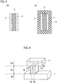
- the switching device comprises: a main circuit 1 including a switching element; a control circuit 2 which generates a control signal for switching the switching element between an on state (conducting state) and an off state (non-conducting state); and a first signal line 3 and a second signal line 4 which transfer the control signal which is outputted from the control circuit 2, to the main circuit 1.
- a switching element 11 included in the main circuit 1 is, for example, a semiconductor element including an IGBT or MOSFET capable of high-speed switching operation.
- Fig. 2 exemplarily shows an IGBT including a collector electrode (C), an emitter electrode (E), and a gate electrode (G).
- the main circuit 1 further includes a first input terminal 12 connected to the gate electrode (G) and a second input terminal 13 connected to the emitter electrode (E).
- the main circuit 1 functions as switching means for performing switching operation with the switching element 11.
- the control circuit 2 generates the control signal in two voltage levels to control two states (on state and off state) of the switching element 11 which is included in the main circuit 1. For example, the control circuit 2 generates, as the control signal, a potential difference (voltage level) between a node between two switching elements (16, 17) connected in series to each other and the other terminal of one of the switching elements, or the switching element 17. The control signal is generated in the different voltage levels in accordance with the on-off states of the switching elements (16, 17).
- the control circuit 2 includes a first output terminal 14 and a second output terminal 15 for outputting the generated control signal. The first output terminal 14 is connected to the node between the two switching elements (16, 17), and the second output terminal 15 is connected to the other terminal of the one switching element 17. The potential difference between the first output terminal 14 and the second output terminal 15 is outputted as the control signal.
- the control circuit 2 thus functions as controlling means for controlling the switching operation of the main circuit 1 with the control signal.
- the first signal line 3 transfers the control signal by connecting the first output terminal 14 and the first input terminal 12 to each other.
- the second signal line 4 transfers the control signal by connecting the second output terminal 15 and the second input terminal 13 to each other.
- the first and second signal lines (3, 4) thus function as transferring means for transferring the control signal.
- the output impedance (Z ab ) of the control circuit 2 which outputs the control signal represents the impedance between the first output terminal 14 and the second output terminal 15.
- the input impedance (Z ef ) of the main circuit 1 to which the control signal is inputted represents the impedance between the first input terminal 12 and the second input terminal 13.
- the value of the characteristic impedance (Z cd ) of the first and second signal lines (3, 4) which transfer the control signal is adjusted to suppress the reflection of the control signal at each portion where the impedance is discontinuous.
- the value of the characteristic impedance (Z cd ) of the first and second signal lines (3, 4) which transfer the control signal is adjusted and set between the value of the output impedance (Z ab ) of the control circuit 2 which outputs the control signal, and the value of the input impedance (Z ef ) of the main circuit 1 to which the control signal is inputted.
- the impedances Z ab , Z cd , and Z ef satisfy either Inequality (2) or Inequality (3).
- the impedances Z ab , Z cd , and Z ef are expressed by Formula (4), Formula (5), and Formula (6), respectively, where L ab , L cd , and L ef are the inductance components of the impedances Z ab , Z cd , and Z ef , C ab , C cd , and C ef are the capacitance components of the impedances Z ab , Z cd , and Z ef , R ab , R cd , and R ef are the resistance components of the impedances Z ab , Z cd , and Z ef , and G ab , G cd , and G ef are the admittance components of the impedances Z ab , Z cd , and Z ef , respectively.
- ⁇ indicates the angular frequency of the alternating current.
- Z ab R ab + j ⁇ L ab G ab + j ⁇ C ab
- Z cd R cd + j ⁇ L cd G cd + j ⁇ C cd
- Z ef R ef + j ⁇ L ef G ef + j ⁇ C ef
- the real parts (R cd , G cd ) of the characteristic impedance Z cd are generally small enough to be negligible as compared to the real parts (R ab , G ab , R ef , G ef ) of the output impedance Z ab and the input impedance Z ef .
- the characteristic impedance Z cd of the first and second signal lines (3, 4) can then be approximated as shown in Formula (7).
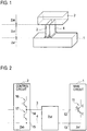
- the self-inductance Lo and the mutual inductance Mo are approximated by Formula (9) and Formula (10), respectively, in a case where the first and second signal lines (3, 4) are formed of flat plates parallel to each other. As shown in Fig. 3 , the length, width, and height of each of the first and second signal lines (3, 4) is 1, w, and H, respectively, and the distance between the first signal line 3 and the second signal line 4 is d.
- [Math. 9] L o ⁇ ⁇ 0 l 2 ⁇ ln 2 l w + H + 1 2 + 0.2235 w + H l
- the capacitance component C cd of the characteristic impedance Z cd is approximated by Formula (11), where ⁇ r is relative permittivity between the first signal line 3 and the second signal line 4, ⁇ 0 is vacuum permittivity, and S is the area of the mutually facing surfaces of the first signal line 3 and the second signal line 4. Note that in the first embodiment, air is filled between the first and second signal lines (3, 4), and thus the relative permittivity ⁇ r is the relative permittivity of air. [Math. 11] C cd ⁇ ⁇ 0 ⁇ r S d
- the characteristic impedance Z cd which is calculated from Formula (7) to Formula (11) is matched to the output impedance Z ab and the input impedance Z ef which are calculated from Formula (4) and Formula (6), such that the absolute values of the reflection coefficients ( ⁇ 1 , ⁇ 2 ) which are shown in Formula (1) can be small.
- the characteristic impedance Z cd is adjusted to satisfy Inequality (2) or Inequality (3).
- the characteristic impedance Z cd may be adjusted using the length (1), width (w), and height (H) of each of the first and second signal lines (3, 4), the distance (d) between the first signal line 3 and the second signal line 4, and the area (S) of the mutually facing surfaces of the first signal line 3 and the second signal line 4.
- Satisfying Inequality (2) or Inequality (3) can suppress the impedance discontinuity between the control circuit 2 and the first and second signal lines (3, 4) and between the first and second signal lines (3, 4) and the main circuit 1 and thus make the absolute values of the reflection coefficients ( ⁇ 1 , ⁇ 2 ) small. This makes it possible to suppress ringing due to the reflection of the control signal between the two terminals (12, 13) of the main circuit 1, and also achieve high-speed performance. Hence, the switching loss can be reduced.
- Satisfying Inequality (2) or Inequality (3) makes the difference between the output impedance (Z ab ) and the characteristic impedance (Z cd ) small and makes the difference between the characteristic impedance (Z cd ) and the input impedance (Z ef ) small.
- This makes it possible to suppress the reflection of the control signal at the nodes between the control circuit 2 and the first and second signal lines (3, 4) and the reflection of the control signal at the nodes between the first and second signal lines (3, 4) and the main circuit 1.
- the ringing noise due to the reflection of the control signal can be reduced with the switching speed of the switching element maintained at high speed.
- the capacitance component (C cd ) of the pair of signal lines can be easily controlled by adjusting the area (S) of and the distance (d) between the mutually facing first and second signal lines (3, 4).
- forming the first and second signal lines (3, 4) with flat plates parallel to each other makes it possible to easily control the characteristic impedance Z cd through adjustment of the parameters (1, w, H, d, S) of the first and second signal lines (3, 4).
- a switching device further comprises a dielectric body 5 disposed between first and second signal lines (3, 4).
- the relative permittivity ( ⁇ r ) is the relative permittivity of air since air is filled between the first and second signal lines (3, 4).
- the dielectric body 5 which is higher in relative permittivity than air is provided between the first and second signal lines (3, 4).
- the capacitance component C cd which is shown in Formula (11) is increased.
- the characteristic impedance Z cd can be reduced to satisfy Inequality (2) or Inequality (3).
- the peripheries of the first and second signal lines (3, 4) with the dielectric body 5 sandwiched therebetween may be covered with resin 6.
- the mechanical strength of the first and second signal lines (3, 4) with the dielectric body 5 sandwiched therebetween can be enhanced.
- the peripheries of the first and second signal lines (3, 4) with air filled therebetween as shown in the first embodiment may be covered with the resin 6.
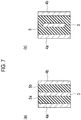
- a switching device comprises one first signal line 3 and two second signal lines (4a, 4b), and the first signal line 3 is disposed between the two second signal lines (4a, 4b).
- Dielectric bodies (5a, 5b) are disposed between the first signal line 3 and the second signal lines (4a, 4b), respectively.
- a capacitance component C cd between the first and second signal lines (3, 4a, 4b) is increased.
- characteristic impedance Z cd of the first and second signal lines (3, 4a, 4b) can be reduced.
- the first signal line 3 and the two second signal lines (4a, 4b) shown in Part (a) of Fig. 7 have an equal width.
- the width (w) of the first signal line 3 may be smaller than the width of each second signal line (4a, 4b), for example.
- the first signal line 3 with its periphery covered with a dielectric body 5 is sandwiched between the two second signal lines (4a, 4b).
- the mechanical strength of the signal lines (3, 4a, 4b) as a whole can be enhanced.
- air may be filled between the first signal line 3 and the second signal lines (4a, 4b).
- a switching device further comprises insulating bodies (7a, 7b) disposed between first and second signal lines (3, 4).
- the first and second signal lines (3, 4) each have a plate shape and are rolled in a state where the insulating bodies (7a, 7b) and the first and second signal lines (3, 4) are superposed one on another.
- a signal line 8 as a whole has a cylindrical shape.
- a capacitance component C cd between the first and second signal lines (3, 4) is increased, and an inductance component L cd is reduced.
- characteristic impedance Z cd of the first and second signal lines can be reduced.
- a first signal line 3 is disposed to surround a second signal line 4.
- the second signal line 4 has a solid cylindrical shape while the first signal line 3 has a hollow cylindrical shape.
- the inner diameter of the first signal line 3 is larger than the outer diameter of the second signal line 4.
- the second signal line 4 is disposed inside the first signal line 3, and a dielectric body 5 is disposed between the second signal line 4 and the first signal line 3.
- a main circuit 1 includes a plurality of switching elements, and a plurality of first and second signal lines (3a, 3b, 3c, ..., 3f, 4a, 4b, 4c, ..., 4g) are provided to transfer a control signal to each of the plurality of switching elements.
- the first and second signal lines (3a to 3f, 4a to 4g) are alternately arranged, and a dielectric body (5a, ...) is disposed between the first and second signal lines.
- a capacitance component C cd between the first and second signal lines (3a to 3f, 4a to 4g) can be increased.
- characteristic impedance Z cd of the first and second signal lines (3a to 3f, 4a to 4g) can be reduced.
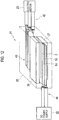
- the switching device can be applied for example to a power converting apparatus 21 which converts DC power outputted from a DC power supply 22 such as a secondary battery into AC power, as shown in Fig. 11 and Fig. 12 .
- the power converting apparatus 21 includes: a power module 25 formed of an inverter 27 which converts the DC power into three-phase AC power and a smoothing capacitor 28 which absorbs fluctuations in the DC voltage to be inputted into the inverter 27; and a metal housing 26 storing the power module 25.
- the inverter 27 includes a plurality of switching elements (31 to 36) capable of high-speed switching operation.
- the inverter 27 includes two switching element for each of the three phases (U phase, V phase, W phase), the two switching elements connected in series to each other and constituting upper and lower arms.
- the inverter 27 is connected in parallel to the DC power supply 22 and the smoothing capacitor 28 by first and second power-feed bus lines.
- the three-phase AC power which is obtained by the conversion by the inverter 27 is fed to an electric motor 23 such as a three-phase AC electric motor.
- the power converting system shown in Fig. 11 and Fig. 12 can be applied to a vehicle that travels with the electric motor 23 as a drive source for travel, i.e. an electric vehicle or hybrid vehicle (HEV) with the output shaft of the electric motor 23 coupled to the vehicle's axle.
- HEV electric vehicle or hybrid vehicle
- the output terminals of the DC power supply 22 are connected to first and second power-feed bus lines 53, 54 in the metal housing 26 by a pair of shield lines 44.
- the control circuit 2 is stored in the metal housing 26 and connected to the plurality of switching elements (31 to 36) by the first and second signal lines, which are not shown.
- the output terminals of the inverter 27 are connected to three shield lines 42 by bus bars 43 disposed in the metal housing 26.
- the three shield lines 42 are connected to the input terminals of the electric motor 23.
- the three-phase AC power which is obtained by the conversion by the inverter 27 is outputted to the electric motor 23 through the bus bars 43 and the shield lines 42.
- the shield lines 42, 44 are each an electric line formed by coating a metal line with resin.
- the switching device according to this embodiment can be applied to the inverter 27 which feeds AC power to the electric motor 23 such as a three-phase AC electric motor.
- the vertical axis in Part (b) of Fig. 13 indicates the amount of ringing peak (RGp) and the switching loss (SLp) in a comparative example in which a gate resistor is provided on a signal line connected to the control terminal (gate terminal) of a switching element, and the amount of ringing peak (RGv) and the switching loss (SLv) in any of the foregoing embodiments of the present invention, in which no gate resistor is provided.
- the horizontal axis in Part (b) of Fig. 13 indicates the gate resistance in the comparative example and the characteristic impedance Z cd of the first and second signal lines (3, 4) in the embodiment of the present invention.
- the larger the gate resistance the smaller the amount of ringing peak (RGp). This is because the larger the gate resistance, the lower the switching speed and the longer the transition time TT and therefore the smaller the ringing noise.
- the gate resistance is so small that the amount of ringing peak (RGp) is larger than a threshold TH for the occurrence of the erroneous operation Ga, the switching loss (SLp) in the comparative example rapidly increases due to the erroneous operation Ga. Even in a range where the amount of ringing peak (RGp) is smaller than the threshold TH, the switching loss (SLp) in the comparative example increases with increase in gate resistance.
- the amount of ringing peak (RGv) in the embodiment starts increasing with increase in characteristic impedance Z cd while the characteristic impedance Z cd satisfies Inequality (2) or Inequality (3). Even if the characteristic impedance Z cd further increases and stops satisfying Inequality (2) or Inequality (3), the amount of ringing peak (RGv) continues to increase further.
- the switching loss (SLv) in the embodiment remains low while the characteristic impedance Z cd satisfies Inequality (2) or Inequality (3), but rapidly increases once the characteristic impedance Z cd stops satisfying Inequality (2) or Inequality (3).
- the switching loss (Gv) in the embodiment can be reduced by 30% or more.
- the real parts of the characteristic impedance Z cd of the first and second signal lines (3, 4) may be ignored and only its imaginary parts (inductance component L cd and capacitance component C cd ) may be taken into consideration. This brings about an advantage that the designing of the characteristic impedance Z cd is easier.
- the characteristic impedance Z cd may be designed by ignoring the inductance component L cd and taking only the capacitance component C cd into consideration.
- the rate of change in the capacitance component (C cd ) between the first bus line and the second bus line is dominant over the rate of change in the inductance component (L cd ) which is shown in Formula (8) to Formula (10).
- the characteristic impedance Z cd can be designed more easily.
Landscapes
- Electronic Switches (AREA)
- Power Conversion In General (AREA)
- Inverter Devices (AREA)
Claims (8)
- Schaltvorrichtung, umfassend:eine Hauptschaltung (1) mit einem Schaltelement (11), einem ersten Eingangsanschluss (12), der mit dem Schaltelement (11) verbunden ist, und einem zweiten Eingangsanschluss (13), der mit dem Schaltelement (11) verbunden ist;eine Steuerschaltung (2), die ein Steuersignal zum Schalten des Schaltelements (11) zwischen einem Ein-Zustand und einem Aus-Zustand erzeugt und einen ersten Ausgangsanschluss (14) und einen zweiten Ausgangsanschluss (15) zum Ausgeben des erzeugten Steuersignals umfasst; undeine erste Signalleitung (3), die den ersten Ausgangsanschluss (14) und den ersten Eingangsanschluss (12) verbindet, und eine zweite Signalleitung (4), die den zweiten Ausgangsanschluss (15) und den zweiten Eingangsanschluss (13) verbindet, die das von der Steuerschaltung (2) ausgegebene Steuersignal an die Hauptschaltung (1) übertragen, wobeiein Wert der charakteristischen Impedanz der ersten und zweiten Signalleitungen (3, 4), die das Steuersignal übertragen, zwischen einem Wert der Ausgangsimpedanz der Steuerschaltung (2), die das Steuersignal ausgibt, und einem Wert der Eingangsimpedanz der Hauptschaltung (1) festgelegt ist, in die das Steuersignal eingegeben wird.
- Schaltvorrichtung nach Anspruch 1, wobei die ersten und zweiten Signalleitungen (3, 4) aus zueinander parallelen flachen Platten gebildet sind.
- Schaltvorrichtung nach Anspruch 1 oder 2, umfassend zwei zweite Signalleitungen, wobei die erste Signalleitung (3) zwischen zwei der zweiten Signalleitungen (4a, 4b) angeordnet ist.
- Schaltvorrichtung nach Anspruch 1 oder 2, wobei die erste Signalleitung (3) die zweite Signalleitung (4) umschließend angeordnet ist.
- Schaltvorrichtung nach einem der Ansprüche 1 bis 4, ferner umfassend einen dielektrischen Körper (5), der zwischen der ersten und zweiten Signalleitungen (3, 4) angeordnet ist.
- Schaltvorrichtung nach Anspruch 1, weiterhin umfassend
einen Isolierkörper (7a, 7b), der zwischen den ersten und zweiten Signalleitungen (3, 4) angeordnet ist, wobei
die ersten und zweiten Signalleitungen (3, 4) jeweils eine Plattenform aufweisen und sind in einem Zustand gerollt sind, in dem der Isolierkörper (7a, 7b) und die ersten und zweiten Signalleitungen (3, 4) übereinander liegen. - Schaltvorrichtung nach Anspruch 1, wobei mindestens eine der ersten und zweiten Signalleitungen (3, 4) mit Harz (6) bedeckt ist.
- Schaltvorrichtung nach Anspruch 1 oder 2, wobei
die Hauptschaltung (1) eine Vielzahl der Schaltelemente (31 bis 36) umfasst,
eine Vielzahl der ersten und zweiten Signalleitungen (3a bis 3f, 4a bis 4g) zum Übertragen des Steuersignals an jedes der Vielzahl der Schaltelemente (31 bis 36) vorgesehen sind,
die ersten und zweiten Signalleitungen (3a bis 3f, 4a bis 4g) abwechselnd angeordnet sind, und ein dielektrischer Körper (5a) zwischen den ersten und zweiten Signalleitungen (3a bis 3f, 4a bis 4g) angeordnet ist.
Applications Claiming Priority (2)
| Application Number | Priority Date | Filing Date | Title |
|---|---|---|---|
| JP2013247038 | 2013-11-29 | ||
| PCT/JP2014/079448 WO2015079882A1 (ja) | 2013-11-29 | 2014-11-06 | スイッチング装置 |
Publications (3)
| Publication Number | Publication Date |
|---|---|
| EP3076534A1 EP3076534A1 (de) | 2016-10-05 |
| EP3076534A4 EP3076534A4 (de) | 2017-04-12 |
| EP3076534B1 true EP3076534B1 (de) | 2019-01-09 |
Family
ID=53198830
Family Applications (1)
| Application Number | Title | Priority Date | Filing Date |
|---|---|---|---|
| EP14865677.0A Active EP3076534B1 (de) | 2013-11-29 | 2014-11-06 | Schaltvorrichtung |
Country Status (5)
| Country | Link |
|---|---|
| US (1) | US10312897B2 (de) |
| EP (1) | EP3076534B1 (de) |
| JP (1) | JP6146481B2 (de) |
| CN (1) | CN105993122B (de) |
| WO (1) | WO2015079882A1 (de) |
Citations (2)
| Publication number | Priority date | Publication date | Assignee | Title |
|---|---|---|---|---|
| US6373740B1 (en) * | 1999-07-30 | 2002-04-16 | Micron Technology, Inc. | Transmission lines for CMOS integrated circuits |
| US20050040846A1 (en) * | 2003-07-28 | 2005-02-24 | Kanji Otsuka | Signal transmission system, and signal transmission line |
Family Cites Families (23)
| Publication number | Priority date | Publication date | Assignee | Title |
|---|---|---|---|---|
| US5055721A (en) * | 1989-04-13 | 1991-10-08 | Mitsubishi Denki Kabushiki Kaisha | Drive circuit for igbt device |
| JP2855816B2 (ja) * | 1990-07-25 | 1999-02-10 | 三菱電機株式会社 | 半導体制御装置 |
| JPH05161343A (ja) * | 1991-11-28 | 1993-06-25 | Toshiba F Ee Syst Eng Kk | Mosゲートトランジスタの駆動回路 |
| US5296765A (en) * | 1992-03-20 | 1994-03-22 | Siliconix Incorporated | Driver circuit for sinking current to two supply voltages |
| JP3462032B2 (ja) | 1997-03-04 | 2003-11-05 | 株式会社東芝 | 電力変換装置 |
| JP2000116117A (ja) * | 1998-10-01 | 2000-04-21 | Fuji Electric Co Ltd | 半導体スイッチ素子のゲート接続構造 |
| US7101770B2 (en) | 2002-01-30 | 2006-09-05 | Micron Technology, Inc. | Capacitive techniques to reduce noise in high speed interconnections |
| JP2003309461A (ja) * | 2002-04-15 | 2003-10-31 | Nec Electronics Corp | 出力バッファ回路 |
| JP2004014547A (ja) * | 2002-06-03 | 2004-01-15 | Toshiba Corp | 半導体装置及び容量調節回路 |
| US6577178B1 (en) * | 2002-07-23 | 2003-06-10 | International Business Machines Corporation | Transient gate tunneling current control |
| US7132874B2 (en) * | 2003-04-23 | 2006-11-07 | The Regents Of The University Of Michigan | Linearizing apparatus and method |
| CN1776830A (zh) | 2004-11-16 | 2006-05-24 | 松下电器产业株式会社 | 信号传输电缆及信号传输电缆的制造方法 |
| US7668667B2 (en) * | 2005-03-07 | 2010-02-23 | Microstrain, Inc. | Miniature stimulating and sensing system |
| CN2812397Y (zh) | 2005-11-03 | 2006-08-30 | 杭州华为三康技术有限公司 | 一种脉冲幅度调制开关电源电路 |
| EP1821313A1 (de) * | 2006-02-17 | 2007-08-22 | Sicon Semiconductor AB | Abtast- und Halteschaltung |
| US7768311B2 (en) * | 2006-08-30 | 2010-08-03 | Stmicroelectronics Pvt. Ltd. | Suppressing ringing in high speed CMOS output buffers driving transmission line load |
| US8674823B1 (en) * | 2009-05-12 | 2014-03-18 | Plug ID, LLC. | Power management system |
| JP5460653B2 (ja) * | 2011-07-14 | 2014-04-02 | 本田技研工業株式会社 | 半導体装置 |
| KR101297460B1 (ko) * | 2012-04-24 | 2013-08-16 | 엘에스산전 주식회사 | 게이트 구동 장치 |
| DE112012007247B4 (de) * | 2012-12-21 | 2022-11-10 | Mitsubishi Electric Corporation | Ansteuerschaltung für ein Schaltelement, Leistungsmodul und Kraftfahrzeug |
| JP2014171296A (ja) * | 2013-03-01 | 2014-09-18 | Panasonic Corp | 半導体スイッチ素子の駆動装置 |
| US20150207508A1 (en) * | 2014-01-22 | 2015-07-23 | The Regents Of The University Of Michigan | Level conversion circuit |
| JP6208326B2 (ja) * | 2014-03-10 | 2017-10-04 | 株式会社日立製作所 | 電力変換ユニット、電力変換装置、および電力変換方法 |
-
2014
- 2014-11-06 EP EP14865677.0A patent/EP3076534B1/de active Active
- 2014-11-06 CN CN201480064374.8A patent/CN105993122B/zh active Active
- 2014-11-06 WO PCT/JP2014/079448 patent/WO2015079882A1/ja not_active Ceased
- 2014-11-06 US US15/039,612 patent/US10312897B2/en active Active
- 2014-11-06 JP JP2015550629A patent/JP6146481B2/ja active Active
Patent Citations (2)
| Publication number | Priority date | Publication date | Assignee | Title |
|---|---|---|---|---|
| US6373740B1 (en) * | 1999-07-30 | 2002-04-16 | Micron Technology, Inc. | Transmission lines for CMOS integrated circuits |
| US20050040846A1 (en) * | 2003-07-28 | 2005-02-24 | Kanji Otsuka | Signal transmission system, and signal transmission line |
Also Published As
| Publication number | Publication date |
|---|---|
| US20170264279A1 (en) | 2017-09-14 |
| JPWO2015079882A1 (ja) | 2017-03-16 |
| CN105993122B (zh) | 2018-05-18 |
| CN105993122A (zh) | 2016-10-05 |
| EP3076534A4 (de) | 2017-04-12 |
| JP6146481B2 (ja) | 2017-06-14 |
| US10312897B2 (en) | 2019-06-04 |
| WO2015079882A1 (ja) | 2015-06-04 |
| EP3076534A1 (de) | 2016-10-05 |
Similar Documents
| Publication | Publication Date | Title |
|---|---|---|
| US20200007026A1 (en) | Power converter | |
| EP3305018B1 (de) | Stromversorgungsvorrichtung für induktionsheizung | |
| US9610847B2 (en) | Power conversion device | |
| US20170324281A1 (en) | Wireless power trnsfer device | |
| CN102098003A (zh) | 振荡电路及半导体装置 | |
| EP3306799B1 (de) | Stromwandlungsvorrichtung | |
| CN103489854A (zh) | 半导体装置及dc-dc转换器 | |
| US10511267B2 (en) | Power amplifier | |
| CN109314460B (zh) | 电力转换装置 | |
| CN106558982B (zh) | 射频干扰抑制电路 | |
| JP6464580B2 (ja) | 電力変換装置 | |
| US10312897B2 (en) | Switching device | |
| EP3629457B1 (de) | Leistungsmodul | |
| JP6862722B2 (ja) | 電力変換装置 | |
| US12243857B2 (en) | Semiconductor integrated circuit | |
| JP6669253B2 (ja) | 電力変換装置 | |
| CN116388546B (zh) | 利用负电感消除寄生电感的振荡抑制电路及方法 | |
| CN214626715U (zh) | 一种电机逆变器 | |
| US20250330102A1 (en) | Electronic power converter circuit apparatus provided with inverter circuit including bridge circuit with switch elements | |
| US11632041B2 (en) | Power semiconductor module | |
| EP4243264A1 (de) | Schaltkreis und stromversorgungsvorrichtung | |
| JP2021129367A (ja) | スイッチング電源装置 |
Legal Events
| Date | Code | Title | Description |
|---|---|---|---|
| PUAI | Public reference made under article 153(3) epc to a published international application that has entered the european phase |
Free format text: ORIGINAL CODE: 0009012 |
|
| 17P | Request for examination filed |
Effective date: 20160524 |
|
| AK | Designated contracting states |
Kind code of ref document: A1 Designated state(s): AL AT BE BG CH CY CZ DE DK EE ES FI FR GB GR HR HU IE IS IT LI LT LU LV MC MK MT NL NO PL PT RO RS SE SI SK SM TR |
|
| AX | Request for extension of the european patent |
Extension state: BA ME |
|
| DAX | Request for extension of the european patent (deleted) | ||
| REG | Reference to a national code |
Ref country code: DE Ref legal event code: R079 Ref document number: 602014039795 Country of ref document: DE Free format text: PREVIOUS MAIN CLASS: H02M0001080000 Ipc: H03K0017160000 |
|
| A4 | Supplementary search report drawn up and despatched |
Effective date: 20170315 |
|
| RIC1 | Information provided on ipc code assigned before grant |
Ipc: H03K 17/0412 20060101ALI20170309BHEP Ipc: H03K 17/16 20060101AFI20170309BHEP |
|
| STAA | Information on the status of an ep patent application or granted ep patent |
Free format text: STATUS: EXAMINATION IS IN PROGRESS |
|
| 17Q | First examination report despatched |
Effective date: 20180201 |
|
| GRAP | Despatch of communication of intention to grant a patent |
Free format text: ORIGINAL CODE: EPIDOSNIGR1 |
|
| STAA | Information on the status of an ep patent application or granted ep patent |
Free format text: STATUS: GRANT OF PATENT IS INTENDED |
|
| INTG | Intention to grant announced |
Effective date: 20180926 |
|
| GRAS | Grant fee paid |
Free format text: ORIGINAL CODE: EPIDOSNIGR3 |
|
| GRAA | (expected) grant |
Free format text: ORIGINAL CODE: 0009210 |
|
| STAA | Information on the status of an ep patent application or granted ep patent |
Free format text: STATUS: THE PATENT HAS BEEN GRANTED |
|
| AK | Designated contracting states |
Kind code of ref document: B1 Designated state(s): AL AT BE BG CH CY CZ DE DK EE ES FI FR GB GR HR HU IE IS IT LI LT LU LV MC MK MT NL NO PL PT RO RS SE SI SK SM TR |
|
| REG | Reference to a national code |
Ref country code: GB Ref legal event code: FG4D |
|
| REG | Reference to a national code |
Ref country code: CH Ref legal event code: EP Ref country code: AT Ref legal event code: REF Ref document number: 1088596 Country of ref document: AT Kind code of ref document: T Effective date: 20190115 |
|
| REG | Reference to a national code |
Ref country code: IE Ref legal event code: FG4D |
|
| REG | Reference to a national code |
Ref country code: DE Ref legal event code: R096 Ref document number: 602014039795 Country of ref document: DE |
|
| REG | Reference to a national code |
Ref country code: NL Ref legal event code: MP Effective date: 20190109 |
|
| REG | Reference to a national code |
Ref country code: LT Ref legal event code: MG4D |
|
| PG25 | Lapsed in a contracting state [announced via postgrant information from national office to epo] |
Ref country code: NL Free format text: LAPSE BECAUSE OF FAILURE TO SUBMIT A TRANSLATION OF THE DESCRIPTION OR TO PAY THE FEE WITHIN THE PRESCRIBED TIME-LIMIT Effective date: 20190109 |
|
| REG | Reference to a national code |
Ref country code: AT Ref legal event code: MK05 Ref document number: 1088596 Country of ref document: AT Kind code of ref document: T Effective date: 20190109 |
|
| PG25 | Lapsed in a contracting state [announced via postgrant information from national office to epo] |
Ref country code: FI Free format text: LAPSE BECAUSE OF FAILURE TO SUBMIT A TRANSLATION OF THE DESCRIPTION OR TO PAY THE FEE WITHIN THE PRESCRIBED TIME-LIMIT Effective date: 20190109 Ref country code: LT Free format text: LAPSE BECAUSE OF FAILURE TO SUBMIT A TRANSLATION OF THE DESCRIPTION OR TO PAY THE FEE WITHIN THE PRESCRIBED TIME-LIMIT Effective date: 20190109 Ref country code: PT Free format text: LAPSE BECAUSE OF FAILURE TO SUBMIT A TRANSLATION OF THE DESCRIPTION OR TO PAY THE FEE WITHIN THE PRESCRIBED TIME-LIMIT Effective date: 20190509 Ref country code: ES Free format text: LAPSE BECAUSE OF FAILURE TO SUBMIT A TRANSLATION OF THE DESCRIPTION OR TO PAY THE FEE WITHIN THE PRESCRIBED TIME-LIMIT Effective date: 20190109 Ref country code: PL Free format text: LAPSE BECAUSE OF FAILURE TO SUBMIT A TRANSLATION OF THE DESCRIPTION OR TO PAY THE FEE WITHIN THE PRESCRIBED TIME-LIMIT Effective date: 20190109 Ref country code: SE Free format text: LAPSE BECAUSE OF FAILURE TO SUBMIT A TRANSLATION OF THE DESCRIPTION OR TO PAY THE FEE WITHIN THE PRESCRIBED TIME-LIMIT Effective date: 20190109 Ref country code: NO Free format text: LAPSE BECAUSE OF FAILURE TO SUBMIT A TRANSLATION OF THE DESCRIPTION OR TO PAY THE FEE WITHIN THE PRESCRIBED TIME-LIMIT Effective date: 20190409 |
|
| PG25 | Lapsed in a contracting state [announced via postgrant information from national office to epo] |
Ref country code: RS Free format text: LAPSE BECAUSE OF FAILURE TO SUBMIT A TRANSLATION OF THE DESCRIPTION OR TO PAY THE FEE WITHIN THE PRESCRIBED TIME-LIMIT Effective date: 20190109 Ref country code: HR Free format text: LAPSE BECAUSE OF FAILURE TO SUBMIT A TRANSLATION OF THE DESCRIPTION OR TO PAY THE FEE WITHIN THE PRESCRIBED TIME-LIMIT Effective date: 20190109 Ref country code: IS Free format text: LAPSE BECAUSE OF FAILURE TO SUBMIT A TRANSLATION OF THE DESCRIPTION OR TO PAY THE FEE WITHIN THE PRESCRIBED TIME-LIMIT Effective date: 20190509 Ref country code: LV Free format text: LAPSE BECAUSE OF FAILURE TO SUBMIT A TRANSLATION OF THE DESCRIPTION OR TO PAY THE FEE WITHIN THE PRESCRIBED TIME-LIMIT Effective date: 20190109 Ref country code: BG Free format text: LAPSE BECAUSE OF FAILURE TO SUBMIT A TRANSLATION OF THE DESCRIPTION OR TO PAY THE FEE WITHIN THE PRESCRIBED TIME-LIMIT Effective date: 20190409 Ref country code: GR Free format text: LAPSE BECAUSE OF FAILURE TO SUBMIT A TRANSLATION OF THE DESCRIPTION OR TO PAY THE FEE WITHIN THE PRESCRIBED TIME-LIMIT Effective date: 20190410 |
|
| REG | Reference to a national code |
Ref country code: DE Ref legal event code: R097 Ref document number: 602014039795 Country of ref document: DE |
|
| PG25 | Lapsed in a contracting state [announced via postgrant information from national office to epo] |
Ref country code: DK Free format text: LAPSE BECAUSE OF FAILURE TO SUBMIT A TRANSLATION OF THE DESCRIPTION OR TO PAY THE FEE WITHIN THE PRESCRIBED TIME-LIMIT Effective date: 20190109 Ref country code: AT Free format text: LAPSE BECAUSE OF FAILURE TO SUBMIT A TRANSLATION OF THE DESCRIPTION OR TO PAY THE FEE WITHIN THE PRESCRIBED TIME-LIMIT Effective date: 20190109 Ref country code: EE Free format text: LAPSE BECAUSE OF FAILURE TO SUBMIT A TRANSLATION OF THE DESCRIPTION OR TO PAY THE FEE WITHIN THE PRESCRIBED TIME-LIMIT Effective date: 20190109 Ref country code: IT Free format text: LAPSE BECAUSE OF FAILURE TO SUBMIT A TRANSLATION OF THE DESCRIPTION OR TO PAY THE FEE WITHIN THE PRESCRIBED TIME-LIMIT Effective date: 20190109 Ref country code: RO Free format text: LAPSE BECAUSE OF FAILURE TO SUBMIT A TRANSLATION OF THE DESCRIPTION OR TO PAY THE FEE WITHIN THE PRESCRIBED TIME-LIMIT Effective date: 20190109 Ref country code: CZ Free format text: LAPSE BECAUSE OF FAILURE TO SUBMIT A TRANSLATION OF THE DESCRIPTION OR TO PAY THE FEE WITHIN THE PRESCRIBED TIME-LIMIT Effective date: 20190109 Ref country code: SK Free format text: LAPSE BECAUSE OF FAILURE TO SUBMIT A TRANSLATION OF THE DESCRIPTION OR TO PAY THE FEE WITHIN THE PRESCRIBED TIME-LIMIT Effective date: 20190109 Ref country code: AL Free format text: LAPSE BECAUSE OF FAILURE TO SUBMIT A TRANSLATION OF THE DESCRIPTION OR TO PAY THE FEE WITHIN THE PRESCRIBED TIME-LIMIT Effective date: 20190109 |
|
| PLBE | No opposition filed within time limit |
Free format text: ORIGINAL CODE: 0009261 |
|
| STAA | Information on the status of an ep patent application or granted ep patent |
Free format text: STATUS: NO OPPOSITION FILED WITHIN TIME LIMIT |
|
| PG25 | Lapsed in a contracting state [announced via postgrant information from national office to epo] |
Ref country code: SM Free format text: LAPSE BECAUSE OF FAILURE TO SUBMIT A TRANSLATION OF THE DESCRIPTION OR TO PAY THE FEE WITHIN THE PRESCRIBED TIME-LIMIT Effective date: 20190109 |
|
| 26N | No opposition filed |
Effective date: 20191010 |
|
| PG25 | Lapsed in a contracting state [announced via postgrant information from national office to epo] |
Ref country code: SI Free format text: LAPSE BECAUSE OF FAILURE TO SUBMIT A TRANSLATION OF THE DESCRIPTION OR TO PAY THE FEE WITHIN THE PRESCRIBED TIME-LIMIT Effective date: 20190109 |
|
| PG25 | Lapsed in a contracting state [announced via postgrant information from national office to epo] |
Ref country code: TR Free format text: LAPSE BECAUSE OF FAILURE TO SUBMIT A TRANSLATION OF THE DESCRIPTION OR TO PAY THE FEE WITHIN THE PRESCRIBED TIME-LIMIT Effective date: 20190109 |
|
| REG | Reference to a national code |
Ref country code: CH Ref legal event code: PL |
|
| PG25 | Lapsed in a contracting state [announced via postgrant information from national office to epo] |
Ref country code: LI Free format text: LAPSE BECAUSE OF NON-PAYMENT OF DUE FEES Effective date: 20191130 Ref country code: MC Free format text: LAPSE BECAUSE OF FAILURE TO SUBMIT A TRANSLATION OF THE DESCRIPTION OR TO PAY THE FEE WITHIN THE PRESCRIBED TIME-LIMIT Effective date: 20190109 Ref country code: CH Free format text: LAPSE BECAUSE OF NON-PAYMENT OF DUE FEES Effective date: 20191130 Ref country code: LU Free format text: LAPSE BECAUSE OF NON-PAYMENT OF DUE FEES Effective date: 20191106 |
|
| REG | Reference to a national code |
Ref country code: BE Ref legal event code: MM Effective date: 20191130 |
|
| PG25 | Lapsed in a contracting state [announced via postgrant information from national office to epo] |
Ref country code: IE Free format text: LAPSE BECAUSE OF NON-PAYMENT OF DUE FEES Effective date: 20191106 |
|
| PG25 | Lapsed in a contracting state [announced via postgrant information from national office to epo] |
Ref country code: BE Free format text: LAPSE BECAUSE OF NON-PAYMENT OF DUE FEES Effective date: 20191130 |
|
| PG25 | Lapsed in a contracting state [announced via postgrant information from national office to epo] |
Ref country code: CY Free format text: LAPSE BECAUSE OF FAILURE TO SUBMIT A TRANSLATION OF THE DESCRIPTION OR TO PAY THE FEE WITHIN THE PRESCRIBED TIME-LIMIT Effective date: 20190109 |
|
| PG25 | Lapsed in a contracting state [announced via postgrant information from national office to epo] |
Ref country code: HU Free format text: LAPSE BECAUSE OF FAILURE TO SUBMIT A TRANSLATION OF THE DESCRIPTION OR TO PAY THE FEE WITHIN THE PRESCRIBED TIME-LIMIT; INVALID AB INITIO Effective date: 20141106 Ref country code: MT Free format text: LAPSE BECAUSE OF FAILURE TO SUBMIT A TRANSLATION OF THE DESCRIPTION OR TO PAY THE FEE WITHIN THE PRESCRIBED TIME-LIMIT Effective date: 20190109 |
|
| PG25 | Lapsed in a contracting state [announced via postgrant information from national office to epo] |
Ref country code: MK Free format text: LAPSE BECAUSE OF FAILURE TO SUBMIT A TRANSLATION OF THE DESCRIPTION OR TO PAY THE FEE WITHIN THE PRESCRIBED TIME-LIMIT Effective date: 20190109 |
|
| PGFP | Annual fee paid to national office [announced via postgrant information from national office to epo] |
Ref country code: DE Payment date: 20251022 Year of fee payment: 12 |
|
| PGFP | Annual fee paid to national office [announced via postgrant information from national office to epo] |
Ref country code: GB Payment date: 20251023 Year of fee payment: 12 |
|
| PGFP | Annual fee paid to national office [announced via postgrant information from national office to epo] |
Ref country code: FR Payment date: 20251022 Year of fee payment: 12 |