EP3074812B1 - Matrix circuit substrate, display apparatus, and manufacturing method of matrix circuit substrate - Google Patents
Matrix circuit substrate, display apparatus, and manufacturing method of matrix circuit substrate Download PDFInfo
- Publication number
- EP3074812B1 EP3074812B1 EP14815264.8A EP14815264A EP3074812B1 EP 3074812 B1 EP3074812 B1 EP 3074812B1 EP 14815264 A EP14815264 A EP 14815264A EP 3074812 B1 EP3074812 B1 EP 3074812B1
- Authority
- EP
- European Patent Office
- Prior art keywords
- substrate
- conductive material
- matrix circuit
- sidewall
- circuit substrate
- Prior art date
- Legal status (The legal status is an assumption and is not a legal conclusion. Google has not performed a legal analysis and makes no representation as to the accuracy of the status listed.)
- Active
Links
Images


Classifications
-
- G—PHYSICS
- G02—OPTICS
- G02F—OPTICAL DEVICES OR ARRANGEMENTS FOR THE CONTROL OF LIGHT BY MODIFICATION OF THE OPTICAL PROPERTIES OF THE MEDIA OF THE ELEMENTS INVOLVED THEREIN; NON-LINEAR OPTICS; FREQUENCY-CHANGING OF LIGHT; OPTICAL LOGIC ELEMENTS; OPTICAL ANALOGUE/DIGITAL CONVERTERS
- G02F1/00—Devices or arrangements for the control of the intensity, colour, phase, polarisation or direction of light arriving from an independent light source, e.g. switching, gating or modulating; Non-linear optics
- G02F1/01—Devices or arrangements for the control of the intensity, colour, phase, polarisation or direction of light arriving from an independent light source, e.g. switching, gating or modulating; Non-linear optics for the control of the intensity, phase, polarisation or colour
- G02F1/13—Devices or arrangements for the control of the intensity, colour, phase, polarisation or direction of light arriving from an independent light source, e.g. switching, gating or modulating; Non-linear optics for the control of the intensity, phase, polarisation or colour based on liquid crystals, e.g. single liquid crystal display cells
- G02F1/133—Constructional arrangements; Operation of liquid crystal cells; Circuit arrangements
- G02F1/1333—Constructional arrangements; Manufacturing methods
- G02F1/13338—Input devices, e.g. touch panels
-
- G—PHYSICS
- G02—OPTICS
- G02F—OPTICAL DEVICES OR ARRANGEMENTS FOR THE CONTROL OF LIGHT BY MODIFICATION OF THE OPTICAL PROPERTIES OF THE MEDIA OF THE ELEMENTS INVOLVED THEREIN; NON-LINEAR OPTICS; FREQUENCY-CHANGING OF LIGHT; OPTICAL LOGIC ELEMENTS; OPTICAL ANALOGUE/DIGITAL CONVERTERS
- G02F1/00—Devices or arrangements for the control of the intensity, colour, phase, polarisation or direction of light arriving from an independent light source, e.g. switching, gating or modulating; Non-linear optics
- G02F1/01—Devices or arrangements for the control of the intensity, colour, phase, polarisation or direction of light arriving from an independent light source, e.g. switching, gating or modulating; Non-linear optics for the control of the intensity, phase, polarisation or colour
- G02F1/13—Devices or arrangements for the control of the intensity, colour, phase, polarisation or direction of light arriving from an independent light source, e.g. switching, gating or modulating; Non-linear optics for the control of the intensity, phase, polarisation or colour based on liquid crystals, e.g. single liquid crystal display cells
- G02F1/133—Constructional arrangements; Operation of liquid crystal cells; Circuit arrangements
- G02F1/1333—Constructional arrangements; Manufacturing methods
- G02F1/133308—Support structures for LCD panels, e.g. frames or bezels
-
- G—PHYSICS
- G02—OPTICS
- G02F—OPTICAL DEVICES OR ARRANGEMENTS FOR THE CONTROL OF LIGHT BY MODIFICATION OF THE OPTICAL PROPERTIES OF THE MEDIA OF THE ELEMENTS INVOLVED THEREIN; NON-LINEAR OPTICS; FREQUENCY-CHANGING OF LIGHT; OPTICAL LOGIC ELEMENTS; OPTICAL ANALOGUE/DIGITAL CONVERTERS
- G02F1/00—Devices or arrangements for the control of the intensity, colour, phase, polarisation or direction of light arriving from an independent light source, e.g. switching, gating or modulating; Non-linear optics
- G02F1/01—Devices or arrangements for the control of the intensity, colour, phase, polarisation or direction of light arriving from an independent light source, e.g. switching, gating or modulating; Non-linear optics for the control of the intensity, phase, polarisation or colour
- G02F1/13—Devices or arrangements for the control of the intensity, colour, phase, polarisation or direction of light arriving from an independent light source, e.g. switching, gating or modulating; Non-linear optics for the control of the intensity, phase, polarisation or colour based on liquid crystals, e.g. single liquid crystal display cells
- G02F1/133—Constructional arrangements; Operation of liquid crystal cells; Circuit arrangements
- G02F1/1333—Constructional arrangements; Manufacturing methods
- G02F1/1335—Structural association of cells with optical devices, e.g. polarisers or reflectors
- G02F1/133509—Filters, e.g. light shielding masks
- G02F1/133514—Colour filters
-
- G—PHYSICS
- G02—OPTICS
- G02F—OPTICAL DEVICES OR ARRANGEMENTS FOR THE CONTROL OF LIGHT BY MODIFICATION OF THE OPTICAL PROPERTIES OF THE MEDIA OF THE ELEMENTS INVOLVED THEREIN; NON-LINEAR OPTICS; FREQUENCY-CHANGING OF LIGHT; OPTICAL LOGIC ELEMENTS; OPTICAL ANALOGUE/DIGITAL CONVERTERS
- G02F1/00—Devices or arrangements for the control of the intensity, colour, phase, polarisation or direction of light arriving from an independent light source, e.g. switching, gating or modulating; Non-linear optics
- G02F1/01—Devices or arrangements for the control of the intensity, colour, phase, polarisation or direction of light arriving from an independent light source, e.g. switching, gating or modulating; Non-linear optics for the control of the intensity, phase, polarisation or colour
- G02F1/13—Devices or arrangements for the control of the intensity, colour, phase, polarisation or direction of light arriving from an independent light source, e.g. switching, gating or modulating; Non-linear optics for the control of the intensity, phase, polarisation or colour based on liquid crystals, e.g. single liquid crystal display cells
- G02F1/133—Constructional arrangements; Operation of liquid crystal cells; Circuit arrangements
- G02F1/1333—Constructional arrangements; Manufacturing methods
- G02F1/1343—Electrodes
- G02F1/134309—Electrodes characterised by their geometrical arrangement
- G02F1/134336—Matrix
-
- G—PHYSICS
- G02—OPTICS
- G02F—OPTICAL DEVICES OR ARRANGEMENTS FOR THE CONTROL OF LIGHT BY MODIFICATION OF THE OPTICAL PROPERTIES OF THE MEDIA OF THE ELEMENTS INVOLVED THEREIN; NON-LINEAR OPTICS; FREQUENCY-CHANGING OF LIGHT; OPTICAL LOGIC ELEMENTS; OPTICAL ANALOGUE/DIGITAL CONVERTERS
- G02F1/00—Devices or arrangements for the control of the intensity, colour, phase, polarisation or direction of light arriving from an independent light source, e.g. switching, gating or modulating; Non-linear optics
- G02F1/01—Devices or arrangements for the control of the intensity, colour, phase, polarisation or direction of light arriving from an independent light source, e.g. switching, gating or modulating; Non-linear optics for the control of the intensity, phase, polarisation or colour
- G02F1/13—Devices or arrangements for the control of the intensity, colour, phase, polarisation or direction of light arriving from an independent light source, e.g. switching, gating or modulating; Non-linear optics for the control of the intensity, phase, polarisation or colour based on liquid crystals, e.g. single liquid crystal display cells
- G02F1/133—Constructional arrangements; Operation of liquid crystal cells; Circuit arrangements
- G02F1/1333—Constructional arrangements; Manufacturing methods
- G02F1/1343—Electrodes
- G02F1/13439—Electrodes characterised by their electrical, optical, physical properties; materials therefor; method of making
-
- G—PHYSICS
- G02—OPTICS
- G02F—OPTICAL DEVICES OR ARRANGEMENTS FOR THE CONTROL OF LIGHT BY MODIFICATION OF THE OPTICAL PROPERTIES OF THE MEDIA OF THE ELEMENTS INVOLVED THEREIN; NON-LINEAR OPTICS; FREQUENCY-CHANGING OF LIGHT; OPTICAL LOGIC ELEMENTS; OPTICAL ANALOGUE/DIGITAL CONVERTERS
- G02F1/00—Devices or arrangements for the control of the intensity, colour, phase, polarisation or direction of light arriving from an independent light source, e.g. switching, gating or modulating; Non-linear optics
- G02F1/01—Devices or arrangements for the control of the intensity, colour, phase, polarisation or direction of light arriving from an independent light source, e.g. switching, gating or modulating; Non-linear optics for the control of the intensity, phase, polarisation or colour
- G02F1/13—Devices or arrangements for the control of the intensity, colour, phase, polarisation or direction of light arriving from an independent light source, e.g. switching, gating or modulating; Non-linear optics for the control of the intensity, phase, polarisation or colour based on liquid crystals, e.g. single liquid crystal display cells
- G02F1/133—Constructional arrangements; Operation of liquid crystal cells; Circuit arrangements
- G02F1/1333—Constructional arrangements; Manufacturing methods
- G02F1/1345—Conductors connecting electrodes to cell terminals
- G02F1/13452—Conductors connecting driver circuitry and terminals of panels
-
- G—PHYSICS
- G02—OPTICS
- G02F—OPTICAL DEVICES OR ARRANGEMENTS FOR THE CONTROL OF LIGHT BY MODIFICATION OF THE OPTICAL PROPERTIES OF THE MEDIA OF THE ELEMENTS INVOLVED THEREIN; NON-LINEAR OPTICS; FREQUENCY-CHANGING OF LIGHT; OPTICAL LOGIC ELEMENTS; OPTICAL ANALOGUE/DIGITAL CONVERTERS
- G02F1/00—Devices or arrangements for the control of the intensity, colour, phase, polarisation or direction of light arriving from an independent light source, e.g. switching, gating or modulating; Non-linear optics
- G02F1/01—Devices or arrangements for the control of the intensity, colour, phase, polarisation or direction of light arriving from an independent light source, e.g. switching, gating or modulating; Non-linear optics for the control of the intensity, phase, polarisation or colour
- G02F1/13—Devices or arrangements for the control of the intensity, colour, phase, polarisation or direction of light arriving from an independent light source, e.g. switching, gating or modulating; Non-linear optics for the control of the intensity, phase, polarisation or colour based on liquid crystals, e.g. single liquid crystal display cells
- G02F1/133—Constructional arrangements; Operation of liquid crystal cells; Circuit arrangements
- G02F1/1333—Constructional arrangements; Manufacturing methods
- G02F1/1345—Conductors connecting electrodes to cell terminals
- G02F1/13454—Drivers integrated on the active matrix substrate
-
- G—PHYSICS
- G02—OPTICS
- G02F—OPTICAL DEVICES OR ARRANGEMENTS FOR THE CONTROL OF LIGHT BY MODIFICATION OF THE OPTICAL PROPERTIES OF THE MEDIA OF THE ELEMENTS INVOLVED THEREIN; NON-LINEAR OPTICS; FREQUENCY-CHANGING OF LIGHT; OPTICAL LOGIC ELEMENTS; OPTICAL ANALOGUE/DIGITAL CONVERTERS
- G02F1/00—Devices or arrangements for the control of the intensity, colour, phase, polarisation or direction of light arriving from an independent light source, e.g. switching, gating or modulating; Non-linear optics
- G02F1/01—Devices or arrangements for the control of the intensity, colour, phase, polarisation or direction of light arriving from an independent light source, e.g. switching, gating or modulating; Non-linear optics for the control of the intensity, phase, polarisation or colour
- G02F1/13—Devices or arrangements for the control of the intensity, colour, phase, polarisation or direction of light arriving from an independent light source, e.g. switching, gating or modulating; Non-linear optics for the control of the intensity, phase, polarisation or colour based on liquid crystals, e.g. single liquid crystal display cells
- G02F1/133—Constructional arrangements; Operation of liquid crystal cells; Circuit arrangements
- G02F1/1333—Constructional arrangements; Manufacturing methods
- G02F1/1345—Conductors connecting electrodes to cell terminals
- G02F1/13458—Terminal pads
-
- G—PHYSICS
- G02—OPTICS
- G02F—OPTICAL DEVICES OR ARRANGEMENTS FOR THE CONTROL OF LIGHT BY MODIFICATION OF THE OPTICAL PROPERTIES OF THE MEDIA OF THE ELEMENTS INVOLVED THEREIN; NON-LINEAR OPTICS; FREQUENCY-CHANGING OF LIGHT; OPTICAL LOGIC ELEMENTS; OPTICAL ANALOGUE/DIGITAL CONVERTERS
- G02F1/00—Devices or arrangements for the control of the intensity, colour, phase, polarisation or direction of light arriving from an independent light source, e.g. switching, gating or modulating; Non-linear optics
- G02F1/01—Devices or arrangements for the control of the intensity, colour, phase, polarisation or direction of light arriving from an independent light source, e.g. switching, gating or modulating; Non-linear optics for the control of the intensity, phase, polarisation or colour
- G02F1/13—Devices or arrangements for the control of the intensity, colour, phase, polarisation or direction of light arriving from an independent light source, e.g. switching, gating or modulating; Non-linear optics for the control of the intensity, phase, polarisation or colour based on liquid crystals, e.g. single liquid crystal display cells
- G02F1/133—Constructional arrangements; Operation of liquid crystal cells; Circuit arrangements
- G02F1/136—Liquid crystal cells structurally associated with a semi-conducting layer or substrate, e.g. cells forming part of an integrated circuit
- G02F1/1362—Active matrix addressed cells
- G02F1/136286—Wiring, e.g. gate line, drain line
-
- G—PHYSICS
- G02—OPTICS
- G02F—OPTICAL DEVICES OR ARRANGEMENTS FOR THE CONTROL OF LIGHT BY MODIFICATION OF THE OPTICAL PROPERTIES OF THE MEDIA OF THE ELEMENTS INVOLVED THEREIN; NON-LINEAR OPTICS; FREQUENCY-CHANGING OF LIGHT; OPTICAL LOGIC ELEMENTS; OPTICAL ANALOGUE/DIGITAL CONVERTERS
- G02F1/00—Devices or arrangements for the control of the intensity, colour, phase, polarisation or direction of light arriving from an independent light source, e.g. switching, gating or modulating; Non-linear optics
- G02F1/01—Devices or arrangements for the control of the intensity, colour, phase, polarisation or direction of light arriving from an independent light source, e.g. switching, gating or modulating; Non-linear optics for the control of the intensity, phase, polarisation or colour
- G02F1/13—Devices or arrangements for the control of the intensity, colour, phase, polarisation or direction of light arriving from an independent light source, e.g. switching, gating or modulating; Non-linear optics for the control of the intensity, phase, polarisation or colour based on liquid crystals, e.g. single liquid crystal display cells
- G02F1/133—Constructional arrangements; Operation of liquid crystal cells; Circuit arrangements
- G02F1/136—Liquid crystal cells structurally associated with a semi-conducting layer or substrate, e.g. cells forming part of an integrated circuit
- G02F1/1362—Active matrix addressed cells
- G02F1/1368—Active matrix addressed cells in which the switching element is a three-electrode device
-
- G—PHYSICS
- G06—COMPUTING OR CALCULATING; COUNTING
- G06F—ELECTRIC DIGITAL DATA PROCESSING
- G06F3/00—Input arrangements for transferring data to be processed into a form capable of being handled by the computer; Output arrangements for transferring data from processing unit to output unit, e.g. interface arrangements
- G06F3/01—Input arrangements or combined input and output arrangements for interaction between user and computer
- G06F3/03—Arrangements for converting the position or the displacement of a member into a coded form
- G06F3/041—Digitisers, e.g. for touch screens or touch pads, characterised by the transducing means
- G06F3/0412—Digitisers structurally integrated in a display
-
- G—PHYSICS
- G02—OPTICS
- G02F—OPTICAL DEVICES OR ARRANGEMENTS FOR THE CONTROL OF LIGHT BY MODIFICATION OF THE OPTICAL PROPERTIES OF THE MEDIA OF THE ELEMENTS INVOLVED THEREIN; NON-LINEAR OPTICS; FREQUENCY-CHANGING OF LIGHT; OPTICAL LOGIC ELEMENTS; OPTICAL ANALOGUE/DIGITAL CONVERTERS
- G02F2201/00—Constructional arrangements not provided for in groups G02F1/00 - G02F7/00
- G02F2201/42—Arrangements for providing conduction through an insulating substrate
Definitions
- the present invention relates to the field of display apparatus, and more in particular to matrix circuit substrates for use in such apparatus and their manufacture.
- a matrix circuit substrate has electrodes distributed in a crisscross arrangement, and is electrically connected to a drive circuit board via a flexible printed circuit (flexible print circuit, FPC), and also connected to an external control chip.
- FPC flexible print circuit
- a connection with an external control chip via a flexible printed circuit allows the emission of light by each pixel of the display panel to be controlled in order to display a picture.
- the matrix circuit substrate of the touch layer in addition to the requirement to connect the matrix circuit substrate of the display panel electrically to a drive circuit via a flexible printed circuit, the matrix circuit substrate of the touch layer must similarly be electrically connected to another flexible printed circuit, and similarly connected to an external control chip via this flexible printed circuit, in order to interact with the electrodes of the electrode layer, which react to the panel being touched by a user.
- a drive circuit board has a definite volume, and the way in which it is configured is the main factor affecting the volume of the display apparatus and display panel.
- a drive circuit board is disposed at the back of the display panel, and the electrodes are connected electrically to the drive circuit board by a flexible printed circuit, in order to reduce the space occupied by the display apparatus as a whole.
- a space must be left around the periphery of the matrix circuit substrate for outer lead bonding (OLB); in other words, the crisscrossing electrodes on the matrix circuit substrate each extend and are brought together in the outer lead bonding space, in order to be connected electrically to the flexible printed circuit.
- OLB outer lead bonding
- the space left around the periphery of the matrix circuit substrate for outer lead bonding in turn increases the width of the rim of the display apparatus, with the result that the display apparatus gives the visual impression of not being sufficiently compact and aesthetically pleasing.
- a display panel and a touch panel each require a flexible printed circuit, so a touch display apparatus will have an increased volume.
- today's users are demanding that display devices or touch display devices are ever lighter and thinner.
- a matrix circuit substrate according to the preamble of claim 1 is known from EP 2 138 892 .
- An advantage of embodiments of the present invention is a narrower rim region by virtue of a novel structural design, so as to form a lighter and thinner structure.
- the present invention proposes a matrix circuit substrate as defined in claim 1, comprising a substrate body, multiple electrodes and at least one first conductive material.
- the substrate body has a first surface and a second surface which are opposite each other, and at least one side surface, which is also called sidewall in the following, located between the first surface and the second surface, the sidewall having at least one recess.
- the electrodes are disposed in a crisscross arrangement on the first surface.
- the first conductive material is disposed in the recess to correspond to at least one of the electrodes, and is electrically connected to the electrode, wherein the recess does not extend to said second surface.
- an electrical connection is enabled between an electrical connection element and the first conductive material in a direction parallel to the sidewall.
- corresponding is meant to indicate that the conductive material is physically arranged in such a way as to enable electrical contact between the conductive material and the targeted electrode.
- the cross sectional area of the recess on the sidewall is larger than the cross sectional area of the electrode.
- the matrix circuit substrate further comprises an electrical connection element, which is electrically connected to the first conductive material.
- the matrix circuit substrate further comprises a second conductive material, disposed on the sidewall between the electrical connection element and the first conductive material, to connect the first conductive material electrically to the electrical connection element.
- the matrix circuit substrate further comprises a control circuit electrically connected to the electrical connection element.
- the recess extends to the first surface.
- the first conductive material can be in direct contact with electrodes disposed on the first surface of the substrate.
- At least one electrode extends to the juncture of the recess and the first surface, so as to be connected electrically with the first conductive material.
- the first conductive material can be in direct contact with electrodes in the most compact way.
- the cross sectional area of the recess on the sidewall is smaller than the maximum cross sectional area of the recess in a direction parallel to the sidewall.
- This geometric arrangement ensures that the first conductive material remains positively engaged, i.e. locked inside the recess.
- the present invention also proposes a display apparatus as defined in claim 7, comprising a matrix circuit substrate and a display medium.
- the matrix circuit substrate comprises a substrate body, multiple electrodes and at least one first conductive material.
- the substrate body has a first surface and a second surface which are opposite each other, and at least one sidewall located between the first surface and the second surface, the sidewall having at least one first recess.
- the electrodes are disposed in a crisscross arrangement on the first surface.
- the first conductive material is disposed in the first recess to correspond to at least one of the electrodes, and is electrically connected to the electrode.
- the matrix circuit substrate drives the display medium.
- the display apparatus further comprises a counter substrate disposed opposite the matrix circuit substrate.
- a sidewall of the counter substrate has at least one second recess, and the first conductive material is also disposed in the second recess.
- the counter substrate further includes a third conductive material, a sidewall of the counter substrate also having at least one second recess in which the third conductive material is disposed.
- the first conductive material is electrically connected to a circuit of the counter substrate.
- the present invention proposes another display apparatus, comprising a matrix circuit substrate, a counter substrate, at least one first conductive material and a display medium.
- the matrix circuit substrate has multiple electrodes disposed in a crisscross arrangement.
- the counter substrate is disposed opposite the matrix circuit substrate, and a sidewall of the counter substrate has at least one recess.
- the first conductive material is disposed in the recess of the counter substrate to correspond to at least one of the electrodes, and is electrically connected to the electrode.
- the matrix circuit substrate drives the display medium.
- the cross sectional area of the recess on the sidewall is larger than the cross sectional area of the electrode.
- the present invention also proposes a method for manufacturing a matrix circuit substrate, as defined in claim 12, comprising the following steps: machining e.g. drilling a mother substrate to form at least one hole that does not run all the way through the mother substrate, wherein the mother substrate has multiple electrodes in a crisscross configuration; filling the hole with a first conductive material, wherein at least one electrode is electrically connected to the first conductive material; subtractive machining e.g. cutting the mother substrate to form at least one substrate body, each substrate body having a first surface and a second surface opposite each other and at least one sidewall located between the first surface and the second surface; and subtractive machining e.g. grinding the sidewall up to the hole, so that the hole forms a recess in the sidewall and the first conductive material is exposed on the sidewall.
- the interconnections between the electrodes on the surface of the substrate and the controller can be formed in a fast and accurate manner, by drilling transverse holes prior to subtractive machining such as sawing or cutting and/or grinding the substrate to the required size.
- the matrix circuit substrate thus produced has the technical advantages described above.
- the method for manufacturing a matrix circuit substrate further comprises the following step: curing the first conductive material with which the hole is filled.
- the curing may be active (e.g., by applying heat) or passive. Curing includes vulcanizing and cross-linking. It is an advantage of this embodiment, that the cured conductive material will be able to withstand the subsequent machining steps (in particular, grinding) that are applied to the substrate.
- the method for manufacturing a matrix circuit substrate further comprises the following step: joining an electrical connection element to the sidewall, so that the electrical connection element is electrically connected to the first conductive material.
- the step of subtractive machining such as grinding the sidewall comprises grinding up to the hole to form a recess, the cross sectional area of the recess on the sidewall being larger than the cross sectional area of the electrode.
- Fig. 1A is a partial schematic diagram of a matrix circuit substrate of a first embodiment of the present invention.
- the matrix circuit substrate 1 comprises a substrate body 11, multiple electrodes 12 and at least one first conductive material 13.
- the materials of the matrix circuit substrate 1 may include resin, metal, ceramic, glass, plastic or other translucent materials, and the substrate may be used for all sorts of display panels, for example TFT substrates of liquid crystal display (LCD) panels, light-emitting diode (LED) display panels or organic light-emitting diode (OLED) display panels, e-paper (e-books), or touch substrates of touch panels.
- the substrate body 11 has a first surface 111 and a second surface 112 opposite each other, and at least one sidewall 113.
- the first surface 111 and the second surface 112 are preferably substantially planar and are major surfaces of the substrate body 11. The required degree of smoothness or flatness of the functional surface will be determined by the nature of the application of the substrate.
- the sidewall 113 is located along a periphery of the substrate, and extends between the first surface 111 and the second surface 112, and preferably, the sidewall 113 is substantially perpendicular to the first surface 111 and second surface 112.
- the electrodes 12 are disposed in a crisscross arrangement on the first surface 111, to form a matrix circuit. If the matrix circuit substrate 1 of this embodiment is used in display apparatus (panels) of various types, the electrodes 12 may be data lines or scan lines. If the matrix circuit substrate 1 of this embodiment is used in a touch substrate, the electrodes 12 may be sensing electrodes which form an X-Y matrix (X-Y sensor).
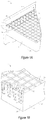
- Fig. 1B is a schematic diagram of the substrate body, electrodes and first conductive material shown in Fig. 1A , viewed from another angle.
- the sidewall 113 in this embodiment is not a smooth surface; preferably, there is at least one recess 114 (a first recess) in the sidewall 113, the recess 114 extending to the first surface 111, i.e. the recess 114 is formed at the juncture 115 of the sidewall 113 and the first surface 111.
- multiple recesses 114 arranged in a linear manner are formed in the sidewall 113 of the substrate body 11.
- the recesses 114 could be arranged in the sidewall 113 in a non-linear, irregular manner, to give the sidewall 113 a more uneven surface. It must also be pointed out that in order to make the drawings concise, Figs. 1A and 1B of the present invention show the recesses 114 of the sidewall 113 on just one side. The skilled person will have no difficulty imagining the arrangement of the recess on other sides of the substrate, which may be completely similar and these additional features are within the scope of the present invention.
- the first conductive material 13 is disposed in the recess 114 to correspond to at least one of the electrodes 12, which means, in particular, that it is arranged in such a way as to enable electrical contact between the conductive material 13 and the said one of the electrodes 12.
- the first conductive material 13 is exposed on the first surface 111 and the sidewall 113.
- Each electrode 12 extends to the juncture of a recess 114 and the first surface 111, i.e. to the distribution area of the recess 114 on the first surface 111, so that the first conductive material 13 is electrically connected to the electrodes 12 separately, to form the matrix circuit substrate 1.
- the matrix circuit substrate 1 may further comprise an electrical connection element 14, while the cross sectional area A of the recesses 114 on the sidewall 113 is larger than the cross sectional area A' of the electrodes 12 (as shown in Fig. 1B ); hence that part of the first conductive material 13 which is exposed on the surface of the sidewall 113 can be larger than the cross sectional area A' of the electrodes 12, so that the electrical connection element 14 can be electrically connected to the exposed part of the first conductive material 13 directly by being disposed on the sidewall 113.
- the matrix circuit substrate 1 can be made by following the sequence of steps shown in Fig. 2 .
- Fig. 2 is a schematic flow chart of the method for manufacturing a matrix circuit substrate of one embodiment of the present invention.
- the method for manufacturing a matrix circuit substrate 1 mainly comprises the following steps: subtractive machining e.g. drilling a mother substrate to form at least one hole, wherein the mother substrate has multiple electrodes in a crisscross configuration (step S10 ); filling the hole with a first conductive material, wherein at least one electrode is electrically connected to the first conductive material (step S20 ); subtractive machining e.g.
- step S30 cutting the mother substrate to form at least one substrate body, each substrate body having a first surface and a second surface opposite each other and at least one sidewall located between the first surface and the second surface (step S30 ); and subtractive machining e.g. grinding the sidewall up to the hole, so that the hole forms a recess in the sidewall and the first conductive material is exposed on the sidewall (step S40 ).
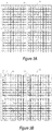
- Fig. 3A is a schematic diagram of step S10 shown in Fig. 2 ;
- Fig. 3B is a schematic diagram of step S20 shown in Fig. 2 .
- Figs. 2 , 3A and 3B shall be jointly referred to.
- a mother substrate 10 is first subtractively machined e.g. drilled to form at least one hole H, which does not run through the mother substrate 10.
- the mother substrate 10 has multiple electrodes 12 in a crisscross configuration.
- the present invention does not place restrictions on the sequence according to which the electrodes 12 are configured.
- the electrodes may be configured on the mother substrate 10 before or after drilling, and may be configured after step S20 in which the hole H is filled with the first conductive material 13; the present invention does not impose any limitation in this respect.
- the electrodes 12 and the first conductive material 13 may be for example indium-tin oxide (ITO) or indium-zinc oxide (IZO), metal, graphene or other conductive materials, but are not limited to these.
- the first conductive material 13 and the electrodes 12 may be of the same or different materials, which may be for example a conductive oxide such as ITO or IZO, but are not limited to these.
- the electrodes 12 are electrically connected to the first conductive material 13, either directly or indirectly.
- a direct electrical connection between the electrodes and the first conductive material 13 is taken as an example. If the electrodes 12 are configured on the mother substrate 10 before or after drilling, the electrical connection between the electrodes 12 and the first conductive material 13 is established after the holes are filled with the first conductive material 13 (step S20 ). In other embodiments, if the electrodes 12 are only configured once the holes H have been filled with the first conductive material 13 in step S20, the electrical connection with the first conductive material is established after configuration of the electrodes 12.
- the electrical connection between the electrodes 12 and the first conductive material 13 is indirect, which means that after configuration of the electrodes 12 is complete and the holes H have been filled with the first conductive material 13, a gap remains between the first conductive material 13 and that end of the electrode 12 which is close to the first conductive material 13, i.e. there is no direct contact between them.
- additional conductive material can be configured in the gap, the method used being for example but not limited to evaporation, sputtering, electroplating, printing, inkjetting, coating or dispensing, in order to establish an indirect electrical connection between the electrodes 12 and the first conductive material 13 via the additionally configured conductive material; the present invention does not impose any limitation in this respect.
- a step S22 in which the first conductive material 13 with which a hole H has been filled is cured, may be further included after step S20 in which the hole is filled with the first conductive material 13.
- the first conductive material 13 may not just be the abovementioned conductive materials, but may also be mixed with another coating, with the manner of curing being determined by the properties of the coating. For example, if a UV-cured coating is added, the first conductive material 13 may be cured directly by UV irradiation; in this embodiment, the first conductive material 13 is cured directly by drying with heat.
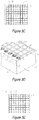
- Fig. 3C is a schematic diagram of step S30 shown in Fig. 2 ; hereinafter, Figs. 2 , 3B and 3C will be jointly referred to.
- the mother substrate 10 is cut to form at least one substrate body 11; in this embodiment, the mother substrate 10 is cut (i.e. cut along the dotted lines in Fig. 3B ) to form four substrate bodies 11. It must be pointed out that Fig. 3C illustrates just one of these substrate bodies 11.
- Fig. 3D is a magnified schematic diagram of part of the substrate body shown in Fig. 3C . Referring to Fig.
- each substrate body 11, as described above, has a first surface 111 and a second surface 112 which are opposite each other and sidewalls 113 which are formed by cutting the mother substrate 10, the sidewalls 13 being located between the first surface 111 and the second surface 112.
- the periphery of the mother substrate 10 is cut in step S30, so that the sidewall 113 of the substrate body 11 is close to the holes H.
- Fig. 3E is a schematic diagram of step S40 shown in Fig. 2 ;
- Fig. 3F is a magnified schematic diagram of part of the substrate body shown in Fig. 3E .
- Fig. 2 and Figs. 3D to 3F will be jointly referred to.
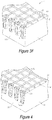
- step S40 the sidewalls 113 (as in Fig. 3D ) are ground to the holes H, so that the holes H form recesses 114 in the sidewalls 113 (as in Fig. 3F ).
- subtractive machining such as grinding is performed until the cross-section of holes H become incomplete circles (as in Fig. 3E ), i.e.
- the process of subtractive machining e.g. grinding the holes H until they form recesses 114 can be split into two stages; specifically, the grinding process may consist of first performing coarse grinding up to the vicinity of the holes H or the edges of the holes H, and then grinding finely (polishing) until the cross sectional area A of the recesses 114 on the sidewall 113 is larger than the cross sectional area A' of the electrodes 12.
- grinding may be continued up to 1/4 to 1/2 of the hole H, i.e.
- the cross sectional area A of the recess 114 on the sidewall 113 (as in Fig. 3 F ) is smaller than the maximum cross sectional area A MAX of the recess 114 in a direction parallel to the sidewall 113, as shown in Fig. 4 , which is a schematic diagram of the maximum cross sectional area of the recesses shown in Fig. 1B in a direction parallel to the sidewall. This figure shall be referred to in conjunction with Fig. 3D .
- the holes H have a substantially round structure, while the maximum cross sectional area A MAX of the recess 114 in a direction parallel to the sidewall 113 is the recess 114 shown in Fig. 4 , formed when the sidewall 113 is ground to the position of the diameter of the hole H, at which point the recess has the maximum cross sectional area A MAX .
- the cross sectional area A of the recess 114 on the sidewall 113 (as shown in Fig.
- the first conductive material 113 that was hardened in step S22 can be prevented from falling out as a result of the grinding process.
- a step S50 may be further included: joining an electrical connection element 14 to the sidewall 113 (as in Fig. 1A ), so that the electrical connection element 14 is electrically connected to the first conductive material 13, wherein the electrical connection element 14 can correspond to multiple first connection materials 13 simultaneously.
- the electrical connection element 14 may be, for example, but is not limited to a data bus, flexible printed circuit (FPC), conductive clip or rigid-flex circuit board, and can be selected according to the apparatus in which the matrix circuit board 1 is used.
- the design of the matrix circuit board 1 of the present invention in which the first conductive material 13 is disposed on the sidewall 113 can further produce the effect of making the rim region narrower.
- Fig. 5 is a schematic diagram of part of a matrix circuit substrate of a second embodiment of the present invention.
- the matrix circuit substrate 1 may further comprise a control circuit 15; one end of the electrical connection element 14 is electrically connected to the first conductive material 13, while the other end of the electrical connection element 14 is electrically connected to the control circuit 15, which is disposed on the second surface 112 of the substrate body 11, and controls the conduction of each electrode 12 on the matrix circuit substrate 1.
- the first and second surfaces 111 and 112 are major surfaces of the substrate 1.
- the control circuit 15 may be for example but is not limited to a printed circuit board (PCB), glass circuit board, or circuit box.
- PCB printed circuit board
- the control circuit 15 may be for example but is not limited to a printed circuit board (PCB), glass circuit board, or circuit box.
- the matrix circuit substrate 1 of this embodiment may further comprise a second conductive material 16, disposed on the sidewall 113 between the electrical connection element 14 and the first conductive material 13, for the purpose of connecting the first conductive material 13 electrically to the electrical connection element 14.
- the second conductive material 16 in this embodiment is anisotropic conductive film (ACF).
- FIG. 6 provides a schematic diagram of part of a matrix circuit substrate.
- the recesses 114a of the matrix circuit substrate 1a of a third embodiment extend not only to the first surface 111a, but also to the second surface 112a, to form a structure in which the recesses 114a run through the substrate body 11 a.
- the surfaces 111a and 112a are major surfaces of the substrate 1a.
- Fig. 2 and Fig. 3A will be jointly referred to.
- holes H which run through the mother substrate 10 can be formed in the step of subtractive machining e.g. drilling to form holes H (i.e. step S10 shown in Fig. 2 ).
- the recesses 114a are a structure extending from the first surface 111a to the second surface 112a.
- the area of contact between the first conductive material 13 a and the electrical connection element 14a can be increased in order to ensure that the electrodes 12a can be electrically connected to the electrical connection element 14a via the first conductive material 13a.
- the conduction of each electrode 12a can similarly be controlled via a control circuit 15a.
- an integrated control circuit can be further disposed directly on the second surface 112a, and electrically connected to the first conductive material 13a of the second surface 112a.
- the integrated control circuit is disposed directly on the second surface 112a of the substrate body 11 a using Chip-On-Glass (COG) technology, and electrically connected to the first conductive material 13a, so that the conduction of each electrode 12a can be controlled via the integrated control circuit.
- COG Chip-On-Glass
- the display apparatus D1 of this embodiment comprises a matrix circuit substrate 1 and a display medium 2.
- the matrix circuit substrate 1 of the second embodiment is used in the display apparatus D1, emission of light by the display medium 2 being driven by the matrix circuit substrate 1.
- the matrix circuit substrates 1 and 1a of the first embodiment may also be used in the display apparatus D1.
- the display medium 2 may be for example but is not limited to liquid crystal material, inorganic LEDs, organic LEDs, phosphor, electrophoretic substance, electroluminescent (EL) material or quantum dots.
- the display medium 2 in this embodiment is liquid crystal material, and the display apparatus D1 is explained using the example of a liquid crystal display (LCD) panel.
- LCD liquid crystal display
- the display apparatus D1 also comprises a counter substrate 3, arranged opposite the matrix circuit substrate 1.
- the counter substrate 3 is a color or monochromatic filter substrate; the example of a color filter (CF) substrate is used here.
- the matrix circuit substrate 1 may be a thin-film transistor (TFT) substrate, and the electrodes 12 may be data lines or scan lines. It may be that only the data lines or the scan lines have an electrical connection with the first conductive material 13, but it may of course be the case that both the data lines and the scan lines have an electrical connection with the first conductive material 13.
- the counter substrate 3 may also be a packaging substrate of an OLED display panel or a top substrate of e-paper (an e-book); this embodiment does not impose any limitation in this respect.
- the display apparatus D1 further comprises a connection element 4, for example rim cement, for connecting the matrix circuit substrate 1 to the counter substrate 3, so that the matrix circuit substrate 1, counter substrate 3 and connection element 4 form a space in which the display medium 2 can be accommodated.
- a backlight module 5 is further included, which may be for example but is not limited to a cold cathode fluorescent lamp (CCFL), hot cathode fluorescent lamp (HCFL), or light emitting diode (LED).
- CCFL cold cathode fluorescent lamp
- HCFL hot cathode fluorescent lamp
- LED light emitting diode
- a sidewall 311 of a substrate body 31 of the counter substrate 3 may similarly have at least one recess 312 (second recess).
- the sidewall 311 and the sidewall 113 shown in Fig. 7 are marked on the side on which there are no recesses 312 or recesses 114, and the counter substrate 3 further includes a third conductive material 33 disposed in the recess 312.
- the recess 312 may also be filled with the first conductive material 13, in other words the recess 312 and the recess 114 may be filled with the same first conductive material 13, or with the third conductive material 33 and the first conductive material 13 (which are different), respectively; the present invention does not impose any limitation in this respect.
- the electrical connection element 14 in this embodiment extends to the counter substrate 3, and since the counter substrate 3 may similarly have recesses 312 filled with the third conductive material 33, the counter substrate 3 may be used as a color filter substrate having an electrode layer, or a touch electrode layer may be added to the counter substrate 3, so that the control circuit 15 can control the conduction of each electrode in the electrode layer or additional touch electrode layer of the counter substrate 3 via the electrical connection element 14, so that the display apparatus D1 may be used as a touch display apparatus.
- the matrix circuit substrate 1a of the third embodiment is used in the display apparatus D2, i.e. emission of light by a display medium 2a is driven by the matrix circuit substrate 1a.
- the matrix circuit substrate 1a is a touch sensing substrate
- electrodes 12a are X-Y sensing electrodes
- a counter substrate 3a is a TFT substrate.
- the matrix circuit substrate 1a and the counter substrate 3a are disposed opposite each other, with a display medium 2a, which is preferably OLEDs, disposed therebetween.
- a connection element 4a which is preferably conductive rim cement, is disposed around the periphery of the display medium 2a, for the purpose of connecting the matrix circuit substrate 1a to the counter substrate 3a.
- Recesses 114a in the matrix circuit substrate 1a of this example extend not only to the first surface 111a but also to the second surface 112a, so the first conductive material 13 a is electrically connected to the circuit of the counter substrate 3a (i.e. the circuit of the TFT substrate itself).
- the first and second surfaces 111a and 112a are major surfaces of the substrate 1a.
- the electrodes 12a of the matrix circuit substrate 1a may be electrically connected to the counter substrate 3a by means of the first conductive material 13 a and the connection element 4a (conductive rim cement).
- the circuit for liquid crystal control which is located on the counter substrate 3a (TFT substrate) can share the control circuit 15 with the matrix circuit substrate 1a (touch sensing substrate), to reduce material costs.
- the display apparatus D3 of this embodiment comprises a matrix circuit substrate 1b, a display medium 2b, a counter substrate 3b and at least one first conductive material 13b.
- the matrix circuit substrate 1b has multiple electrodes 12b disposed in a crisscross arrangement.
- the counter substrate 3b is disposed opposite the matrix circuit substrate 1b.
- the counter substrate 3b as an example, is a color filter substrate, while the matrix circuit substrate 1b, as an example, is a TFT substrate.
- a sidewall 311b of the counter substrate 3b has at least one recess 312b; it must also be pointed out that in order to make the drawing concise, the sidewall 311b is marked on the side which has no recesses 312b.
- the first conductive material 13b corresponds to at least one of the electrodes 12 b and is disposed in the recess 312b of the counter substrate 3b, and the first conductive material 13b is electrically connected to the electrode 12b.
- connection element 4b conductive rim cement
- the electrodes 12b on the matrix circuit substrate 1b can be electrically connected to the counter substrate 3b via the connection element 4b (conductive rim cement), and further connected to other electrical elements via the first conductive material 13b disposed in the recess 312b of the counter substrate 3b.
- the conduction of the electrodes 12b is controlled so as to drive the display medium 2b by means of an electrical connection between an electrical connection element 14b and a first conductive material 13b, and by means of an electrical connection between a control circuit 15b and the electrical connection element 14b.
- a feature which this embodiment has in common with the embodiments described above is that the cross sectional area of the recess 312b on the sidewall 311b is larger than the cross sectional area of the electrode 12b; the matrix circuit substrate 1 of the first embodiment may be referred to for details. Information regarding other related elements and the technical features thereof can also be found above, and is not repeated here.
- a substrate such as a touch sensing substrate, color filter substrate or TFT substrate may be added between the matrix circuit substrate 1b and the counter substrate 3b.
- the counter substrate 3b could be a touch sensing substrate
- the matrix circuit substrate 1b could be a TFT substrate, with a color filter substrate disposed between them.
- the matrix circuit substrate can further comprise an electrical connection element, which is electrically connected to the at least one first conductive material.
- the matrix circuit substrate can further comprise a second conductive material, disposed on the side all between the electrical connection element and the first conductive material, to connect the first conductive material electrically to the electrical connection element.
- the matrix circuit substrate can further comprise a control circuit electrically connected to the electrical connection element.
- the first recess can extend to the first surface.
- At least one of the electrodes extends to the juncture of the recess and the first surface, so as to be electrically connected to the first conductive material.
- an electrical connection is enabled between an electrical connection element and the first conductive material in a direction parallel to the sidewall.
- the electrical connection element can be disposed directly on the sidewall via the electrical connection with the first conductive material.
Landscapes
- Physics & Mathematics (AREA)
- Nonlinear Science (AREA)
- General Physics & Mathematics (AREA)
- Mathematical Physics (AREA)
- Chemical & Material Sciences (AREA)
- Crystallography & Structural Chemistry (AREA)
- Optics & Photonics (AREA)
- Engineering & Computer Science (AREA)
- Microelectronics & Electronic Packaging (AREA)
- General Engineering & Computer Science (AREA)
- Theoretical Computer Science (AREA)
- Geometry (AREA)
- Human Computer Interaction (AREA)
- Devices For Indicating Variable Information By Combining Individual Elements (AREA)
- Liquid Crystal (AREA)
- Electroluminescent Light Sources (AREA)
Description
- The present invention relates to the field of display apparatus, and more in particular to matrix circuit substrates for use in such apparatus and their manufacture.
- As progress is made in science and technology, information devices of all kinds are continuously evolving. This is especially true of the various types of display apparatus or touch display apparatus, which are applied in all sorts of electronic devices, such as mobile phones, flat-screen computers, ultrabooks and e-books. Both the display apparatus and the touch layer thereof are formed by a matrix circuit substrate.
- In general, a matrix circuit substrate has electrodes distributed in a crisscross arrangement, and is electrically connected to a drive circuit board via a flexible printed circuit (flexible print circuit, FPC), and also connected to an external control chip. In the case of display apparatus, a connection with an external control chip via a flexible printed circuit allows the emission of light by each pixel of the display panel to be controlled in order to display a picture. Moreover, in the case of touch display apparatus, in addition to the requirement to connect the matrix circuit substrate of the display panel electrically to a drive circuit via a flexible printed circuit, the matrix circuit substrate of the touch layer must similarly be electrically connected to another flexible printed circuit, and similarly connected to an external control chip via this flexible printed circuit, in order to interact with the electrodes of the electrode layer, which react to the panel being touched by a user.
- However, a drive circuit board has a definite volume, and the way in which it is configured is the main factor affecting the volume of the display apparatus and display panel. In the prior art, a drive circuit board is disposed at the back of the display panel, and the electrodes are connected electrically to the drive circuit board by a flexible printed circuit, in order to reduce the space occupied by the display apparatus as a whole. However, in the prior art, a space must be left around the periphery of the matrix circuit substrate for outer lead bonding (OLB); in other words, the crisscrossing electrodes on the matrix circuit substrate each extend and are brought together in the outer lead bonding space, in order to be connected electrically to the flexible printed circuit.
- However, the space left around the periphery of the matrix circuit substrate for outer lead bonding in turn increases the width of the rim of the display apparatus, with the result that the display apparatus gives the visual impression of not being sufficiently compact and aesthetically pleasing. Moreover, a display panel and a touch panel each require a flexible printed circuit, so a touch display apparatus will have an increased volume. Furthermore, today's users are demanding that display devices or touch display devices are ever lighter and thinner.
- Thus, it remains a challenge to provide a matrix circuit substrate and display apparatus which can have a narrower rim region by virtue of novel structural design, so as to form a lighter and thinner structure.
- A matrix circuit substrate according to the preamble of
claim 1 is known fromEP 2 138 892 . - It is an object of embodiments of the present invention to provide an alternative matrix circuit substrate, display apparatus and/or method for manufacturing a matrix circuit substrate. An advantage of embodiments of the present invention is a narrower rim region by virtue of a novel structural design, so as to form a lighter and thinner structure.
- The present invention proposes a matrix circuit substrate as defined in
claim 1, comprising a substrate body, multiple electrodes and at least one first conductive material. The substrate body has a first surface and a second surface which are opposite each other, and at least one side surface, which is also called sidewall in the following, located between the first surface and the second surface, the sidewall having at least one recess. The electrodes are disposed in a crisscross arrangement on the first surface. The first conductive material is disposed in the recess to correspond to at least one of the electrodes, and is electrically connected to the electrode, wherein the recess does not extend to said second surface. - It is an advantage of the present invention that, by disposing the first conductive material on (and partly inside) the side wall, space can be saved so as to make the rim region narrower as compared to prior art substrates in which an electrical connection element is disposed on the first surface of the substrate body. By forming a recess in a sidewall of the matrix circuit substrate and filling the recess with a first conductive material, an electrical connection is enabled between an electrical connection element and the first conductive material in a direction parallel to the sidewall.
- The term "corresponding" is meant to indicate that the conductive material is physically arranged in such a way as to enable electrical contact between the conductive material and the targeted electrode.
- In one embodiment of the present invention, the cross sectional area of the recess on the sidewall is larger than the cross sectional area of the electrode.
- It is an advantage of this embodiment that it facilitates making further connections to the conductive material in the recesses, from the side. It is a further advantage of this embodiment that it reduces the risk of disengagement between the conductive material and the recess wall during machining and handling of the substrate.
- In one embodiment of the present invention, the matrix circuit substrate further comprises an electrical connection element, which is electrically connected to the first conductive material.
- It is an advantage of this embodiment that the specific geometry of the substrate, i.e. the presence of exposed conducting material connecting to the electrodes on the side of the substrate, is used to simplify electrical access to these electrodes.
- In one embodiment of the present invention, the matrix circuit substrate further comprises a second conductive material, disposed on the sidewall between the electrical connection element and the first conductive material, to connect the first conductive material electrically to the electrical connection element.
- It is an advantage of this embodiment that the overall conductivity of the path between the electrodes and the electrical conductive material is improved. Also, in this manner, geometric discrepancies between the sidewall (in particular, the exposed parts of the first conductive material) and the electrical connection element can easily be bridged.
- In one embodiment of the present invention, the matrix circuit substrate further comprises a control circuit electrically connected to the electrical connection element.
- It is an advantage of this embodiment that the various functions required for a display or touch screen can be combined in a compact arrangement.
- In one embodiment of the present invention, the recess extends to the first surface.
- It is an advantage of this embodiment that the first conductive material can be in direct contact with electrodes disposed on the first surface of the substrate.
- In one embodiment of the present invention, at least one electrode extends to the juncture of the recess and the first surface, so as to be connected electrically with the first conductive material.
- It is an advantage of this embodiment that the first conductive material can be in direct contact with electrodes in the most compact way.
- In one embodiment of the present invention, the cross sectional area of the recess on the sidewall is smaller than the maximum cross sectional area of the recess in a direction parallel to the sidewall.
- This geometric arrangement ensures that the first conductive material remains positively engaged, i.e. locked inside the recess.
- The present invention also proposes a display apparatus as defined in claim 7, comprising a matrix circuit substrate and a display medium. The matrix circuit substrate comprises a substrate body, multiple electrodes and at least one first conductive material. The substrate body has a first surface and a second surface which are opposite each other, and at least one sidewall located between the first surface and the second surface, the sidewall having at least one first recess. The electrodes are disposed in a crisscross arrangement on the first surface. The first conductive material is disposed in the first recess to correspond to at least one of the electrodes, and is electrically connected to the electrode. The matrix circuit substrate drives the display medium.
- The variations of the matrix circuit substrate according to embodiments of the invention, as described above, apply in the same manner to the display apparatus according to the invention which comprises such a matrix circuit substrate.
- In one embodiment of the present invention, the display apparatus further comprises a counter substrate disposed opposite the matrix circuit substrate.
- It is an advantage of this embodiment that the various functions required for a display or touch screen can be combined in a compact arrangement.
- In one embodiment of the present invention, a sidewall of the counter substrate has at least one second recess, and the first conductive material is also disposed in the second recess.
- This is one particularly advantageous way to allow interaction between the matrix circuit substrate and the counter substrate.
- In one embodiment of the present invention, the counter substrate further includes a third conductive material, a sidewall of the counter substrate also having at least one second recess in which the third conductive material is disposed.
- This is another particularly advantageous way to allow interaction between the matrix circuit substrate and the counter substrate.
- In one embodiment of the present invention, the first conductive material is electrically connected to a circuit of the counter substrate.
- This is yet another particularly advantageous way to allow interaction between the matrix circuit substrate and the counter substrate.
- The present invention proposes another display apparatus, comprising a matrix circuit substrate, a counter substrate, at least one first conductive material and a display medium. The matrix circuit substrate has multiple electrodes disposed in a crisscross arrangement. The counter substrate is disposed opposite the matrix circuit substrate, and a sidewall of the counter substrate has at least one recess. The first conductive material is disposed in the recess of the counter substrate to correspond to at least one of the electrodes, and is electrically connected to the electrode. The matrix circuit substrate drives the display medium.
- In one embodiment of the present invention, the cross sectional area of the recess on the sidewall is larger than the cross sectional area of the electrode.
- The present invention also proposes a method for manufacturing a matrix circuit substrate, as defined in
claim 12, comprising the following steps:
machining e.g. drilling a mother substrate to form at least one hole that does not run all the way through the mother substrate, wherein the mother substrate has multiple electrodes in a crisscross configuration; filling the hole with a first conductive material, wherein at least one electrode is electrically connected to the first conductive material; subtractive machining e.g. cutting the mother substrate to form at least one substrate body, each substrate body having a first surface and a second surface opposite each other and at least one sidewall located between the first surface and the second surface; and subtractive machining e.g. grinding the sidewall up to the hole, so that the hole forms a recess in the sidewall and the first conductive material is exposed on the sidewall. - It is an advantage of the method according to the present invention that the interconnections between the electrodes on the surface of the substrate and the controller can be formed in a fast and accurate manner, by drilling transverse holes prior to subtractive machining such as sawing or cutting and/or grinding the substrate to the required size. The matrix circuit substrate thus produced has the technical advantages described above.
- In one embodiment of the present invention, the method for manufacturing a matrix circuit substrate further comprises the following step: curing the first conductive material with which the hole is filled.
- The curing may be active (e.g., by applying heat) or passive. Curing includes vulcanizing and cross-linking. It is an advantage of this embodiment, that the cured conductive material will be able to withstand the subsequent machining steps (in particular, grinding) that are applied to the substrate.
- In one embodiment of the present invention, the method for manufacturing a matrix circuit substrate further comprises the following step: joining an electrical connection element to the sidewall, so that the electrical connection element is electrically connected to the first conductive material.
- It is an advantage of this embodiment that the specific geometry of the substrate, i.e. the presence of exposed conducting material connecting to the electrodes on the side of the substrate, is used to simplify electrical access to these electrodes.
- In one embodiment of the present invention, the step of subtractive machining such as grinding the sidewall comprises grinding up to the hole to form a recess, the cross sectional area of the recess on the sidewall being larger than the cross sectional area of the electrode.
- It is an advantage of this embodiment that it facilitates making further connections to the conductive material in the recesses, from the side. It is a further advantage of this embodiment that it reduces the risk of disengagement between the conductive material and the recess wall during machining and handling of the substrate.
- These and other technical effects and advantages of embodiments of the present invention will now be described in more detail with reference to the accompanying figures, in which:
-
Fig. 1A is a partial schematic diagram of a matrix circuit substrate of a first embodiment of the present invention; -
Fig. 1B is a schematic diagram of the substrate body, electrodes and first conductive material shown inFig. 1A , viewed from another angle; -
Fig. 2 is a schematic flow chart of the method for manufacturing a matrix circuit substrate of one embodiment of the present invention; -
Fig. 3A is a schematic diagram of step S10 shown inFig. 2 ; -
Fig. 3B is a schematic diagram of step S20 shown inFig. 2 ; -
Fig. 3C is a schematic diagram of step S30 shown inFig. 2 ; -
Fig. 3D is a magnified schematic diagram of part of the substrate body shown inFig. 3C ; -
Fig. 3E is a schematic diagram of step S40 shown inFig. 2 ; -
Fig. 3F is a magnified schematic diagram of part of the substrate body shown inFig. 3E ; -
Fig. 4 is a schematic diagram of the maximum cross sectional area of the recesses shown inFig. 1B in a direction parallel to the sidewall; -
Fig. 5 is a schematic diagram of part of a matrix circuit substrate of a second embodiment of the present invention; -
Fig. 6 is a schematic diagram of part of a matrix circuit substrate of a first comparative example; -
Fig. 7 is a schematic sectional drawing of a display apparatus of a third embodiment of the present invention; -
Fig. 8 is a schematic sectional drawing of a display apparatus of a second comparative example; and -
Fig. 9 is a schematic sectional drawing of a display apparatus of a fourth embodiment of the present invention. - Throughout the figures, like elements will be referred to with like reference numerals.
- The matrix circuit substrate, display apparatus and method for manufacturing a matrix circuit substrate according to preferred embodiments of the present invention are explained below with reference to the relevant drawings, in which identical elements are explained using identical reference symbols. The drawings of all the embodiments of the present invention are no more than schematic, and do not represent real dimensions and proportions.
-
Fig. 1A is a partial schematic diagram of a matrix circuit substrate of a first embodiment of the present invention. AsFig. 1A shows, thematrix circuit substrate 1 comprises asubstrate body 11,multiple electrodes 12 and at least one firstconductive material 13. The materials of thematrix circuit substrate 1 may include resin, metal, ceramic, glass, plastic or other translucent materials, and the substrate may be used for all sorts of display panels, for example TFT substrates of liquid crystal display (LCD) panels, light-emitting diode (LED) display panels or organic light-emitting diode (OLED) display panels, e-paper (e-books), or touch substrates of touch panels. Thesubstrate body 11 has afirst surface 111 and asecond surface 112 opposite each other, and at least onesidewall 113. Thefirst surface 111 and thesecond surface 112 are preferably substantially planar and are major surfaces of thesubstrate body 11. The required degree of smoothness or flatness of the functional surface will be determined by the nature of the application of the substrate. Thesidewall 113 is located along a periphery of the substrate, and extends between thefirst surface 111 and thesecond surface 112, and preferably, thesidewall 113 is substantially perpendicular to thefirst surface 111 andsecond surface 112. Theelectrodes 12 are disposed in a crisscross arrangement on thefirst surface 111, to form a matrix circuit. If thematrix circuit substrate 1 of this embodiment is used in display apparatus (panels) of various types, theelectrodes 12 may be data lines or scan lines. If thematrix circuit substrate 1 of this embodiment is used in a touch substrate, theelectrodes 12 may be sensing electrodes which form an X-Y matrix (X-Y sensor). -
Fig. 1B is a schematic diagram of the substrate body, electrodes and first conductive material shown inFig. 1A , viewed from another angle. Hereinafter,Figs. 1A and 1B will be jointly referred to. In addition, thesidewall 113 in this embodiment is not a smooth surface; preferably, there is at least one recess 114 (a first recess) in thesidewall 113, therecess 114 extending to thefirst surface 111, i.e. therecess 114 is formed at thejuncture 115 of thesidewall 113 and thefirst surface 111. In this embodiment,multiple recesses 114 arranged in a linear manner are formed in thesidewall 113 of thesubstrate body 11. In other embodiments, therecesses 114 could be arranged in thesidewall 113 in a non-linear, irregular manner, to give thesidewall 113 a more uneven surface. It must also be pointed out that in order to make the drawings concise,Figs. 1A and 1B of the present invention show therecesses 114 of thesidewall 113 on just one side. The skilled person will have no difficulty imagining the arrangement of the recess on other sides of the substrate, which may be completely similar and these additional features are within the scope of the present invention. - The first
conductive material 13 is disposed in therecess 114 to correspond to at least one of theelectrodes 12, which means, in particular, that it is arranged in such a way as to enable electrical contact between theconductive material 13 and the said one of theelectrodes 12. The firstconductive material 13 is exposed on thefirst surface 111 and thesidewall 113. Eachelectrode 12 extends to the juncture of arecess 114 and thefirst surface 111, i.e. to the distribution area of therecess 114 on thefirst surface 111, so that the firstconductive material 13 is electrically connected to theelectrodes 12 separately, to form thematrix circuit substrate 1. - Furthermore, the
matrix circuit substrate 1 may further comprise anelectrical connection element 14, while the cross sectional area A of therecesses 114 on thesidewall 113 is larger than the cross sectional area A' of the electrodes 12 (as shown inFig. 1B ); hence that part of the firstconductive material 13 which is exposed on the surface of thesidewall 113 can be larger than the cross sectional area A' of theelectrodes 12, so that theelectrical connection element 14 can be electrically connected to the exposed part of the firstconductive material 13 directly by being disposed on thesidewall 113. Specifically, thematrix circuit substrate 1 can be made by following the sequence of steps shown inFig. 2 . -
Fig. 2 is a schematic flow chart of the method for manufacturing a matrix circuit substrate of one embodiment of the present invention. AsFig. 2 shows, the method for manufacturing amatrix circuit substrate 1 mainly comprises the following steps: subtractive machining e.g. drilling a mother substrate to form at least one hole, wherein the mother substrate has multiple electrodes in a crisscross configuration (step S10); filling the hole with a first conductive material, wherein at least one electrode is electrically connected to the first conductive material (step S20); subtractive machining e.g. cutting the mother substrate to form at least one substrate body, each substrate body having a first surface and a second surface opposite each other and at least one sidewall located between the first surface and the second surface (step S30); and subtractive machining e.g. grinding the sidewall up to the hole, so that the hole forms a recess in the sidewall and the first conductive material is exposed on the sidewall (step S40). -
Fig. 3A is a schematic diagram of step S10 shown inFig. 2 ;Fig. 3B is a schematic diagram of step S20 shown inFig. 2 . Hereinafter,Figs. 2 ,3A and 3B shall be jointly referred to. In step S10, amother substrate 10 is first subtractively machined e.g. drilled to form at least one hole H, which does not run through themother substrate 10. Themother substrate 10 hasmultiple electrodes 12 in a crisscross configuration. Of course, the present invention does not place restrictions on the sequence according to which theelectrodes 12 are configured. The electrodes may be configured on themother substrate 10 before or after drilling, and may be configured after step S20 in which the hole H is filled with the firstconductive material 13; the present invention does not impose any limitation in this respect. In this embodiment, theelectrodes 12 and the firstconductive material 13 may be for example indium-tin oxide (ITO) or indium-zinc oxide (IZO), metal, graphene or other conductive materials, but are not limited to these. The firstconductive material 13 and theelectrodes 12 may be of the same or different materials, which may be for example a conductive oxide such as ITO or IZO, but are not limited to these. - As
Fig. 3B shows, theelectrodes 12 are electrically connected to the firstconductive material 13, either directly or indirectly. In this embodiment, a direct electrical connection between the electrodes and the firstconductive material 13 is taken as an example. If theelectrodes 12 are configured on themother substrate 10 before or after drilling, the electrical connection between theelectrodes 12 and the firstconductive material 13 is established after the holes are filled with the first conductive material 13 (step S20). In other embodiments, if theelectrodes 12 are only configured once the holes H have been filled with the firstconductive material 13 in step S20, the electrical connection with the first conductive material is established after configuration of theelectrodes 12. - Furthermore, in other embodiments, the electrical connection between the
electrodes 12 and the firstconductive material 13 is indirect, which means that after configuration of theelectrodes 12 is complete and the holes H have been filled with the firstconductive material 13, a gap remains between the firstconductive material 13 and that end of theelectrode 12 which is close to the firstconductive material 13, i.e. there is no direct contact between them. At this point, additional conductive material can be configured in the gap, the method used being for example but not limited to evaporation, sputtering, electroplating, printing, inkjetting, coating or dispensing, in order to establish an indirect electrical connection between theelectrodes 12 and the firstconductive material 13 via the additionally configured conductive material; the present invention does not impose any limitation in this respect. - Preferably, a step S22, in which the first
conductive material 13 with which a hole H has been filled is cured, may be further included after step S20 in which the hole is filled with the firstconductive material 13. The firstconductive material 13 may not just be the abovementioned conductive materials, but may also be mixed with another coating, with the manner of curing being determined by the properties of the coating. For example, if a UV-cured coating is added, the firstconductive material 13 may be cured directly by UV irradiation; in this embodiment, the firstconductive material 13 is cured directly by drying with heat. -
Fig. 3C is a schematic diagram of step S30 shown inFig. 2 ; hereinafter,Figs. 2 ,3B and3C will be jointly referred to. In step S30, themother substrate 10 is cut to form at least onesubstrate body 11; in this embodiment, themother substrate 10 is cut (i.e. cut along the dotted lines inFig. 3B ) to form foursubstrate bodies 11. It must be pointed out thatFig. 3C illustrates just one of thesesubstrate bodies 11.Fig. 3D is a magnified schematic diagram of part of the substrate body shown inFig. 3C . Referring toFig. 3D , eachsubstrate body 11, as described above, has afirst surface 111 and asecond surface 112 which are opposite each other andsidewalls 113 which are formed by cutting themother substrate 10, thesidewalls 13 being located between thefirst surface 111 and thesecond surface 112. In other embodiments, if themother substrate 10 and thesubstrate body 11 are similar in size, the periphery of themother substrate 10 is cut in step S30, so that thesidewall 113 of thesubstrate body 11 is close to the holes H. -
Fig. 3E is a schematic diagram of step S40 shown inFig. 2 ;Fig. 3F is a magnified schematic diagram of part of the substrate body shown inFig. 3E . Hereinafter,Fig. 2 andFigs. 3D to 3F will be jointly referred to. In step S40, the sidewalls 113 (as inFig. 3D ) are ground to the holes H, so that the holes H form recesses 114 in the sidewalls 113 (as inFig. 3F ). In other words, subtractive machining such as grinding is performed until the cross-section of holes H become incomplete circles (as inFig. 3E ), i.e. recesses 114 are formed in thesidewalls 113, and the firstconductive material 13 is exposed on thesidewalls 113, at which point thematrix circuit substrate 1 is formed. Preferably, the process of subtractive machining e.g. grinding the holes H until they form recesses 114 can be split into two stages; specifically, the grinding process may consist of first performing coarse grinding up to the vicinity of the holes H or the edges of the holes H, and then grinding finely (polishing) until the cross sectional area A of therecesses 114 on thesidewall 113 is larger than the cross sectional area A' of theelectrodes 12. Preferably, grinding may be continued up to 1/4 to 1/2 of the hole H, i.e. not exceed 1/2 of the hole H, so that the firstconductive material 13, which was hardened in step S22, can be prevented from falling out as a result of the grinding process. In other words, the cross sectional area A of therecess 114 on the sidewall 113 (as inFig. 3F ) is smaller than the maximum cross sectional area AMAX of therecess 114 in a direction parallel to thesidewall 113, as shown inFig. 4 , which is a schematic diagram of the maximum cross sectional area of the recesses shown inFig. 1B in a direction parallel to the sidewall. This figure shall be referred to in conjunction withFig. 3D . Viewed from thefirst surface 111, the holes H have a substantially round structure, while the maximum cross sectional area AMAX of therecess 114 in a direction parallel to thesidewall 113 is therecess 114 shown inFig. 4 , formed when thesidewall 113 is ground to the position of the diameter of the hole H, at which point the recess has the maximum cross sectional area AMAX. As the cross sectional area A of therecess 114 on the sidewall 113 (as shown inFig. 1B ) is smaller than the maximum cross sectional area AMAX of therecess 114 in a direction parallel to thesidewall 113 in this embodiment, the firstconductive material 113 that was hardened in step S22 can be prevented from falling out as a result of the grinding process. - As
Fig. 2 shows, after grinding thesidewall 113 up to the hole H to form arecess 114 and exposing the firstconductive material 13 on thesidewall 113 in step S40 (as inFig. 1B ), a step S50 may be further included: joining anelectrical connection element 14 to the sidewall 113 (as inFig. 1A ), so that theelectrical connection element 14 is electrically connected to the firstconductive material 13, wherein theelectrical connection element 14 can correspond to multiplefirst connection materials 13 simultaneously. Theelectrical connection element 14 may be, for example, but is not limited to a data bus, flexible printed circuit (FPC), conductive clip or rigid-flex circuit board, and can be selected according to the apparatus in which thematrix circuit board 1 is used. Thus, compared to prior art in which an electrical connection element is disposed on the first surface of the substrate body, the design of thematrix circuit board 1 of the present invention in which the firstconductive material 13 is disposed on thesidewall 113 can further produce the effect of making the rim region narrower. -
Fig. 5 is a schematic diagram of part of a matrix circuit substrate of a second embodiment of the present invention. InFig. 5 , other components have been added to thematrix circuit substrate 1 of the first embodiment, so the reference symbols used for the latter are retained. AsFig. 5 shows, thematrix circuit substrate 1 may further comprise acontrol circuit 15; one end of theelectrical connection element 14 is electrically connected to the firstconductive material 13, while the other end of theelectrical connection element 14 is electrically connected to thecontrol circuit 15, which is disposed on thesecond surface 112 of thesubstrate body 11, and controls the conduction of eachelectrode 12 on thematrix circuit substrate 1. The first andsecond surfaces substrate 1. Thecontrol circuit 15 may be for example but is not limited to a printed circuit board (PCB), glass circuit board, or circuit box. By disposing the firstconductive material 13 on thesidewall 113 of thematrix circuit substrate 1, not only can the width of the OLB be reduced (there may even be no OLB region), the operation of disposing theelectrical connection element 14 on thesidewall 113 can be facilitated, reducing misalignment of theelectrical connection element 14. Thus, compared to prior art in which an electrical connection element is disposed on the first surface of the substrate body, the design of thematrix circuit board 1 of this embodiment in which the firstconductive material 13 is disposed on thesidewall 113 can further produce the effect of saving space while making the rim region narrower. - Furthermore, as
Fig. 5 shows, thematrix circuit substrate 1 of this embodiment may further comprise a secondconductive material 16, disposed on thesidewall 113 between theelectrical connection element 14 and the firstconductive material 13, for the purpose of connecting the firstconductive material 13 electrically to theelectrical connection element 14. As an example, the secondconductive material 16 in this embodiment is anisotropic conductive film (ACF). - A first comparative example will now be described with reference to
Fig. 6 , which provides a schematic diagram of part of a matrix circuit substrate. Therecesses 114a of the matrix circuit substrate 1a of a third embodiment extend not only to the first surface 111a, but also to thesecond surface 112a, to form a structure in which therecesses 114a run through thesubstrate body 11a. Thesurfaces 111a and 112a are major surfaces of the substrate 1a. Hereinafter,Fig. 2 andFig. 3A will be jointly referred to. In the matrix circuit substrate 1a of this example, holes H which run through themother substrate 10 can be formed in the step of subtractive machining e.g. drilling to form holes H (i.e. step S10 shown inFig. 2 ). Once the matrix circuit substrate 1a has been made, therecesses 114a are a structure extending from the first surface 111a to thesecond surface 112a. In this example, the area of contact between the firstconductive material 13a and theelectrical connection element 14a can be increased in order to ensure that theelectrodes 12a can be electrically connected to theelectrical connection element 14a via the firstconductive material 13a. In addition, the conduction of eachelectrode 12a can similarly be controlled via acontrol circuit 15a. Since therecesses 114a of the matrix circuit substrate 1a extend to thesecond surface 112a, the firstconductive material 13a with which therecesses 114a are filled similarly extends to thesecond surface 112a; thus, apart from controlling the conduction of eachelectrode 12a using acontrol circuit 15a, in other embodiments, an integrated control circuit can be further disposed directly on thesecond surface 112a, and electrically connected to the firstconductive material 13a of thesecond surface 112a. In other words, the integrated control circuit is disposed directly on thesecond surface 112a of thesubstrate body 11a using Chip-On-Glass (COG) technology, and electrically connected to the firstconductive material 13a, so that the conduction of eachelectrode 12a can be controlled via the integrated control circuit. Furthermore, for information regarding other related elements of the matrix circuit substrate 1a of the first comparative example and the configuration in which they are connected to each other, thematrix circuit substrates 1 of the first and second embodiments may be referred to; details will not be repeated here. - A third embodiment of the present invention will now be described with reference to
Fig. 7 , which provides a schematic sectional drawing of a display apparatus. The display apparatus D1 of this embodiment comprises amatrix circuit substrate 1 and a display medium 2. In this embodiment, as an example, thematrix circuit substrate 1 of the second embodiment is used in the display apparatus D1, emission of light by the display medium 2 being driven by thematrix circuit substrate 1. Thus information regarding the characteristics of the related elements of thematrix circuit substrate 1 and the configuration in which they are connected to each other may be found above. Of course, in other embodiments, thematrix circuit substrates 1 and 1a of the first embodiment may also be used in the display apparatus D1. The display medium 2 may be for example but is not limited to liquid crystal material, inorganic LEDs, organic LEDs, phosphor, electrophoretic substance, electroluminescent (EL) material or quantum dots. The display medium 2 in this embodiment is liquid crystal material, and the display apparatus D1 is explained using the example of a liquid crystal display (LCD) panel. - In addition to the
matrix circuit substrate 1, the display apparatus D1 also comprises a counter substrate 3, arranged opposite thematrix circuit substrate 1. In this embodiment, the counter substrate 3 is a color or monochromatic filter substrate; the example of a color filter (CF) substrate is used here. Thematrix circuit substrate 1 may be a thin-film transistor (TFT) substrate, and theelectrodes 12 may be data lines or scan lines. It may be that only the data lines or the scan lines have an electrical connection with the firstconductive material 13, but it may of course be the case that both the data lines and the scan lines have an electrical connection with the firstconductive material 13. In other embodiments, the counter substrate 3 may also be a packaging substrate of an OLED display panel or a top substrate of e-paper (an e-book); this embodiment does not impose any limitation in this respect. The display apparatus D1 further comprises a connection element 4, for example rim cement, for connecting thematrix circuit substrate 1 to the counter substrate 3, so that thematrix circuit substrate 1, counter substrate 3 and connection element 4 form a space in which the display medium 2 can be accommodated. In this embodiment, a backlight module 5 is further included, which may be for example but is not limited to a cold cathode fluorescent lamp (CCFL), hot cathode fluorescent lamp (HCFL), or light emitting diode (LED). - In addition, in this embodiment, a
sidewall 311 of asubstrate body 31 of the counter substrate 3 may similarly have at least one recess 312 (second recess). Special attention must be drawn to the fact that in order to make the drawing concise, thesidewall 311 and thesidewall 113 shown inFig. 7 are marked on the side on which there are norecesses 312 orrecesses 114, and the counter substrate 3 further includes a thirdconductive material 33 disposed in therecess 312. Of course, in other embodiments, therecess 312 may also be filled with the firstconductive material 13, in other words therecess 312 and therecess 114 may be filled with the same firstconductive material 13, or with the thirdconductive material 33 and the first conductive material 13 (which are different), respectively; the present invention does not impose any limitation in this respect. In addition, theelectrical connection element 14 in this embodiment extends to the counter substrate 3, and since the counter substrate 3 may similarly haverecesses 312 filled with the thirdconductive material 33, the counter substrate 3 may be used as a color filter substrate having an electrode layer, or a touch electrode layer may be added to the counter substrate 3, so that thecontrol circuit 15 can control the conduction of each electrode in the electrode layer or additional touch electrode layer of the counter substrate 3 via theelectrical connection element 14, so that the display apparatus D1 may be used as a touch display apparatus. - A second comparative example will now be described with reference to
Fig. 8 , which provides a schematic sectional drawing of a display apparatus. In this example, as an example, the matrix circuit substrate 1a of the third embodiment is used in the display apparatus D2, i.e. emission of light by adisplay medium 2a is driven by the matrix circuit substrate 1a. Thus information regarding the characteristics of the related elements of the matrix circuit substrate 1a and the configuration in which they are connected to each other may be found above. In this example, as an example, the matrix circuit substrate 1a is a touch sensing substrate,electrodes 12a are X-Y sensing electrodes, and, as an example, a counter substrate 3a is a TFT substrate. The matrix circuit substrate 1a and the counter substrate 3a are disposed opposite each other, with adisplay medium 2a, which is preferably OLEDs, disposed therebetween. Aconnection element 4a, which is preferably conductive rim cement, is disposed around the periphery of thedisplay medium 2a, for the purpose of connecting the matrix circuit substrate 1a to the counter substrate 3a.Recesses 114a in the matrix circuit substrate 1a of this example extend not only to the first surface 111a but also to thesecond surface 112a, so the firstconductive material 13a is electrically connected to the circuit of the counter substrate 3a (i.e. the circuit of the TFT substrate itself). The first andsecond surfaces 111a and 112a are major surfaces of the substrate 1a. Specifically, theelectrodes 12a of the matrix circuit substrate 1a may be electrically connected to the counter substrate 3a by means of the firstconductive material 13a and theconnection element 4a (conductive rim cement). Thus the circuit for liquid crystal control which is located on the counter substrate 3a (TFT substrate) can share thecontrol circuit 15 with the matrix circuit substrate 1a (touch sensing substrate), to reduce material costs. - A fourth embodiment of the present invention will now be described with reference to
Fig. 9 , which provides a schematic sectional drawing of a display apparatus. The display apparatus D3 of this embodiment comprises a matrix circuit substrate 1b, adisplay medium 2b, acounter substrate 3b and at least one firstconductive material 13b. The matrix circuit substrate 1b has multiple electrodes 12b disposed in a crisscross arrangement. Thecounter substrate 3b is disposed opposite the matrix circuit substrate 1b. In this embodiment, thecounter substrate 3b, as an example, is a color filter substrate, while the matrix circuit substrate 1b, as an example, is a TFT substrate. Asidewall 311b of thecounter substrate 3b has at least onerecess 312b; it must also be pointed out that in order to make the drawing concise, thesidewall 311b is marked on the side which has norecesses 312b. The firstconductive material 13b corresponds to at least one of the electrodes 12b and is disposed in therecess 312b of thecounter substrate 3b, and the firstconductive material 13b is electrically connected to the electrode 12b. Specifically, by using conductive rim cement as the principal material of aconnection element 4b disposed around the periphery of thedisplay medium 2b, and having therecess 312b extend to the surface on the side close to theconnection element 4b, the electrodes 12b on the matrix circuit substrate 1b can be electrically connected to thecounter substrate 3b via theconnection element 4b (conductive rim cement), and further connected to other electrical elements via the firstconductive material 13b disposed in therecess 312b of thecounter substrate 3b. In this embodiment, the conduction of the electrodes 12b is controlled so as to drive thedisplay medium 2b by means of an electrical connection between anelectrical connection element 14b and a firstconductive material 13b, and by means of an electrical connection between acontrol circuit 15b and theelectrical connection element 14b. A feature which this embodiment has in common with the embodiments described above is that the cross sectional area of therecess 312b on thesidewall 311b is larger than the cross sectional area of the electrode 12b; thematrix circuit substrate 1 of the first embodiment may be referred to for details. Information regarding other related elements and the technical features thereof can also be found above, and is not repeated here. - Of course, as is known by those skilled in the art, in other embodiments of the present invention, a substrate such as a touch sensing substrate, color filter substrate or TFT substrate may be added between the matrix circuit substrate 1b and the
counter substrate 3b. For example, thecounter substrate 3b could be a touch sensing substrate, and the matrix circuit substrate 1b could be a TFT substrate, with a color filter substrate disposed between them. - Various exemplary aspects of the present invention are as follows:
The matrix circuit substrate can further comprise an electrical connection element, which is electrically connected to the at least one first conductive material. - The matrix circuit substrate can further comprise a second conductive material, disposed on the side all between the electrical connection element and the first conductive material, to connect the first conductive material electrically to the electrical connection element.
- The matrix circuit substrate can further comprise a control circuit electrically connected to the electrical connection element.
- The first recess can extend to the first surface.
- At least one of the electrodes extends to the juncture of the recess and the first surface, so as to be electrically connected to the first conductive material.
- In summary, in the matrix circuit substrate and display apparatus of embodiments of the present invention, by forming a recess in a sidewall of the matrix circuit substrate and filling the recess with a first conductive material, an electrical connection is enabled between an electrical connection element and the first conductive material in a direction parallel to the sidewall. In other words, the electrical connection element can be disposed directly on the sidewall via the electrical connection with the first conductive material. Thus, compared to prior art in which an electrical connection element is disposed on the first surface of the substrate body, the design of the matrix circuit board of the present invention in which the first conductive material is disposed on the sidewall can further produce the effect of saving space while making the rim region narrower.
Claims (15)
- A matrix circuit substrate (1; 1a; 1b), comprising:a substrate body (11; 11a; 11b), having a first surface (111; 111a) and a second surface (112; 112a) which are opposite each other, and at least one side surface of a sidewall (113; 113a; 113b) located between the first surface (111; 111a) and the second surface (112; 112a), the at least one side surface of the sidewall (113; 113a; 113b) having at least one recess (114; 114a; 114b); multiple electrodes (12; 12a; 12b), disposed in a crisscross arrangement on the first surface (111; 111a); andat least one first conductive material (13; 13a; 13b), disposed in the recess (114; 114a; 114b) to correspond to at least one of the electrodes (12; 12a; 12b), and electrically connected to the electrode (12; 12a; 12b),characterized in
thatsaid recess does not extend to said second surface (112; 112a). - The matrix circuit substrate (1; 1a; 1b) according to Claim 1, wherein the cross sectional area (A) of the recess (114; 114a; 114b) on the at least one side surface of the sidewall (113; 113a; 113b) is larger than the cross sectional area (A') of the electrode (12; 12a; 12b) in the plane defined by said at least one side surface of the sidewall (113; 113a; 113b).
- The matrix circuit substrate (1; 1a; 1b) according to Claim 1 or Claim 2, further comprising:
an electrical connection element (14; 14a; 14b), which is electrically connected to the first conductive material (13; 13a; 13b). - The matrix circuit substrate (1; 1a; 1b) according to Claim 3, further comprising:
a second conductive material (16), disposed on the at least one side surface of the sidewall (113) between the electrical connection element (14) and the first conductive material (13), to connect the first conductive material (13) electrically to the electrical connection element (14) . - The matrix circuit substrate (1; 1a; 1b) according to Claim 3, further comprising:
a control circuit (15; 15a; 15b) electrically connected to the electrical connection element (14). - The matrix circuit substrate (1; 1a; 1b) according to any of the preceding claims, wherein the recess (114; 114a; 114b; 312; 312b) extends to the first surface (111; 111a).
- A display apparatus (Dl; D2; D3), comprising:a matrix circuit substrate (1; 1a; 1b) according to any of the preceding claims; anda display medium (2; 2a; 2b), driven by the matrix circuit substrate (1; 1a; 1b).
- The display apparatus (Dl; D2; D3) according to Claim 7, further comprising:
a counter substrate (3; 3a; 3b) disposed opposite the matrix circuit substrate (1; 1a; 1b). - The display apparatus (D3) according to Claim 8, wherein a side surface of a sidewall (311b) of the counter substrate (3b) has at least one second recess (312b), and the first conductive material (13b) is also disposed in the second recess (312b).
- The display apparatus (D1) according to Claim 8, wherein the counter substrate (3) further includes a third conductive material (33), a side surface of the sidewall (311) of the counter substrate (3) also having at least one second recess (312) in which the third conductive material (33) is disposed.
- Display apparatus (D2) according to Claim 8, wherein the first conductive material (13a) is electrically connected to a circuit of the counter substrate (3a).
- A method for manufacturing a matrix circuit substrate (1; 1a; 1b), the method comprising the following steps:drilling (S10) a mother substrate (10) to form at least one hole (H) that does not run all the way through said mother substrate (10), wherein the mother substrate (10) has multiple electrodes (12; 12a; 12b) in a crisscross configuration;filling (S20) the hole (H) with a first conductive material (13; 13a; 13b), wherein at least one of the electrodes (12; 12a; 12b) is electrically connected to the first conductive material (13; 13a; 13b);cutting (S30) the mother substrate (10) to form at least one substrate body (11; 11a; 11b), each substrate body (11; 11a; 11b) having a first surface (111; 111a) and a second surface (112; 112a) opposite each other and at least one side surface of a sidewall (113; 113a; 113b) located between the first surface (111; 111a) and the second surface (112; 112b); andgrinding (S40) the at least one side surface of the sidewall (113; 113a) up to the hole (H), so that the hole (H) forms a recess (114; 114a; 114b) in the at least one side surface of the sidewall (113; 113a) and the first conductive material (13; 13a; 13b) is exposed on the at least one side surface of the sidewall(113; 113a).
- The method according to Claim 12, further comprising: curing (S22) the first conductive material (13; 13a; 13b) with which the hole (H) is filled.
- The method according to Claim 12, further comprising: joining (S50) an electrical connection element(14) to the sidewall (113), so that the electrical connection element(14) is electrically connected to the first conductive material (13) .
- The method according to claim 12, wherein the step of grinding (S40) the at least one side surface of the side wall (113; 113a) comprises grinding up to the hole (H) to form a recess (114; 114a; 114b), the cross sectional area of the recess (114; 114a; 114b) on the at least one side surface of the sidewall (113; 113a)being larger than the cross sectional area (A') of the electrode (12; 12a; 12b).
Applications Claiming Priority (3)
| Application Number | Priority Date | Filing Date | Title |
|---|---|---|---|
| TW102143533A TWI532087B (en) | 2013-10-25 | 2013-11-28 | Matrix circuit substrate, display apparatus and manufacturing method of matrix circuit substrate |
| CN201310645843.2A CN104678625A (en) | 2013-11-28 | 2013-12-04 | Matrix circuit board, display device, and method for manufacturing matrix circuit board |
| PCT/EP2014/076030 WO2015079058A1 (en) | 2013-11-28 | 2014-11-28 | Matrix circuit substrate, display apparatus, and manufacturing method of matrix circuit substrate |
Publications (2)
| Publication Number | Publication Date |
|---|---|
| EP3074812A1 EP3074812A1 (en) | 2016-10-05 |
| EP3074812B1 true EP3074812B1 (en) | 2019-03-27 |
Family
ID=52130220
Family Applications (1)
| Application Number | Title | Priority Date | Filing Date |
|---|---|---|---|
| EP14815264.8A Active EP3074812B1 (en) | 2013-11-28 | 2014-11-28 | Matrix circuit substrate, display apparatus, and manufacturing method of matrix circuit substrate |
Country Status (5)
| Country | Link |
|---|---|
| US (2) | US10156748B2 (en) |
| EP (1) | EP3074812B1 (en) |
| JP (1) | JP6511468B2 (en) |
| KR (1) | KR20170065462A (en) |
| WO (1) | WO2015079058A1 (en) |
Families Citing this family (18)
| Publication number | Priority date | Publication date | Assignee | Title |
|---|---|---|---|---|
| KR102477579B1 (en) * | 2017-11-15 | 2022-12-13 | 엘지디스플레이 주식회사 | Electronic device having a touch sensor and display device |
| US10319802B1 (en) * | 2017-11-22 | 2019-06-11 | Microsoft Technology Licensing, Llc | Display substrate edge patterning and metallization |
| KR102464097B1 (en) * | 2017-12-28 | 2022-11-07 | 삼성디스플레이 주식회사 | Display device |
| JP7287637B2 (en) * | 2018-10-04 | 2023-06-06 | 株式会社Nsc | Liquid crystal panel manufacturing method |
| KR20210068124A (en) * | 2018-10-04 | 2021-06-08 | 코닝 인코포레이티드 | Systems and methods for manufacturing displays including recessed side electrodes |
| TWI720446B (en) * | 2019-03-25 | 2021-03-01 | 佳世達科技股份有限公司 | Display pannel and mrthod for fabricating the same |
| TWI722405B (en) * | 2019-03-28 | 2021-03-21 | 佳世達科技股份有限公司 | Display pannel |
| KR102848691B1 (en) | 2019-07-23 | 2025-08-22 | 삼성디스플레이 주식회사 | Display device and method of manufacturing the same |
| KR20210016237A (en) * | 2019-08-02 | 2021-02-15 | 삼성디스플레이 주식회사 | Display device, manufacturing method thereof, and multi display device |
| US11444120B2 (en) * | 2020-01-14 | 2022-09-13 | Au Optronics Corporation | Display apparatus and method of fabricating the same |
| TWI835978B (en) | 2020-01-22 | 2024-03-21 | 晶元光電股份有限公司 | Light-emitting device |
| DE102020202170A1 (en) | 2020-02-20 | 2021-08-26 | OSRAM Opto Semiconductors Gesellschaft mit beschränkter Haftung | OPTOELECTRONIC MODULE AND HEADLAMP WITH AN OPTOELECTRONIC MODULE |
| KR102829217B1 (en) * | 2020-03-03 | 2025-07-04 | 삼성전자주식회사 | Display module having glass substrate formed side wirings and manufacturing mathod as the same |
| EP4068373A4 (en) | 2020-05-08 | 2023-06-07 | Samsung Electronics Co., Ltd. | DISPLAY MODULE COMPRISING A GLASS SUBSTRATE ENCLOSING SIDE WIRING, AND METHOD OF MANUFACTURING THEREOF |
| US11631703B2 (en) | 2020-06-18 | 2023-04-18 | Barco Nv | System and method for display panel |
| LU500367B1 (en) | 2021-06-30 | 2023-01-06 | Barco Nv | Improvements in light emitting modules |
| LU500363B1 (en) | 2021-06-30 | 2023-01-02 | Barco Nv | Optical data transmission in light emitting modules |
| LU500365B1 (en) | 2021-06-30 | 2023-01-02 | Barco Nv | Improvements in light emitting modules |
Family Cites Families (25)
| Publication number | Priority date | Publication date | Assignee | Title |
|---|---|---|---|---|
| US4183629A (en) * | 1976-07-21 | 1980-01-15 | Citizen Watch Co. Ltd. | Electronic optical display device and method of manufacturing the same |
| JPS5784518U (en) | 1980-11-13 | 1982-05-25 | ||
| JPS6150118A (en) | 1984-08-20 | 1986-03-12 | Matsushita Electric Ind Co Ltd | Electric connecting device |
| JPS61167976A (en) | 1985-01-22 | 1986-07-29 | 松下電器産業株式会社 | Liquid crystal display unit |
| JPS61236585A (en) | 1985-04-12 | 1986-10-21 | 松下電器産業株式会社 | liquid crystal display device |
| JPS62111240A (en) | 1985-11-09 | 1987-05-22 | Matsushita Electric Ind Co Ltd | Manufacturing method of liquid crystal display panel |
| US5081063A (en) * | 1989-07-20 | 1992-01-14 | Harris Corporation | Method of making edge-connected integrated circuit structure |
| US5557436A (en) * | 1994-05-12 | 1996-09-17 | Magnascreen Corporation | Thin seal liquid crystal display and method of making same |
| US5889568A (en) * | 1995-12-12 | 1999-03-30 | Rainbow Displays Inc. | Tiled flat panel displays |
| JP3797742B2 (en) | 1997-04-24 | 2006-07-19 | シチズン電子株式会社 | Manufacturing method of liquid crystal display panel |
| JP3856521B2 (en) | 1997-04-24 | 2006-12-13 | シチズン電子株式会社 | Liquid crystal display |
| US6407502B2 (en) * | 1997-09-16 | 2002-06-18 | Lite Array, Inc. | EL display with electrodes normal to the surface |
| JP4298068B2 (en) * | 1998-08-18 | 2009-07-15 | セイコーエプソン株式会社 | ELECTRO-OPTICAL DEVICE, ELECTRONIC DEVICE EQUIPPED WITH THE SAME, AND METHOD FOR PRODUCING ELECTRO-OPTICAL DEVICE |
| JP2001215528A (en) | 2000-02-03 | 2001-08-10 | Matsushita Electric Ind Co Ltd | LCD panel with built-in peripheral drive circuit |
| US6581276B2 (en) * | 2000-04-04 | 2003-06-24 | Amerasia International Technology, Inc. | Fine-pitch flexible connector, and method for making same |
| US6724511B2 (en) * | 2001-11-16 | 2004-04-20 | Thin Film Electronics Asa | Matrix-addressable optoelectronic apparatus and electrode means in the same |
| US7193244B2 (en) * | 2004-04-14 | 2007-03-20 | E. I. Du Pont De Nemours And Company | Electronic devices with edge connectors and methods of using the same |
| KR101120924B1 (en) | 2007-03-20 | 2012-03-13 | 후지쯔 가부시끼가이샤 | Lamination type display element and its manufacturing method |
| KR100927296B1 (en) * | 2007-05-28 | 2009-11-18 | 파나소닉 주식회사 | Organic EL Devices and Displays |
| KR20090058987A (en) * | 2007-12-05 | 2009-06-10 | 엘지디스플레이 주식회사 | Manufacturing method of liquid crystal display device and manufacturing method of film carrier tape of liquid crystal display device |
| KR20090113635A (en) * | 2008-04-28 | 2009-11-02 | 삼성전자주식회사 | Display |
| US8253914B2 (en) * | 2010-06-23 | 2012-08-28 | Microsoft Corporation | Liquid crystal display (LCD) |
| TWI431568B (en) | 2010-09-17 | 2014-03-21 | Au Optronics Corp | Display |
| US10048551B2 (en) | 2012-01-11 | 2018-08-14 | Sharp Kabushiki Kaisha | Semiconductor device, display device, and semiconductor device manufacturing method |
| KR102083987B1 (en) | 2013-06-20 | 2020-03-04 | 삼성디스플레이 주식회사 | Back palne of flat panel display and method for manufacturing the same |
-
2014
- 2014-11-28 JP JP2016555925A patent/JP6511468B2/en active Active
- 2014-11-28 US US15/037,226 patent/US10156748B2/en active Active
- 2014-11-28 EP EP14815264.8A patent/EP3074812B1/en active Active
- 2014-11-28 WO PCT/EP2014/076030 patent/WO2015079058A1/en not_active Ceased
- 2014-11-28 KR KR1020167017241A patent/KR20170065462A/en not_active Withdrawn
-
2018
- 2018-11-08 US US16/184,040 patent/US10545364B2/en active Active
Non-Patent Citations (1)
| Title |
|---|
| None * |
Also Published As
| Publication number | Publication date |
|---|---|
| US20190086705A1 (en) | 2019-03-21 |
| JP2017501453A (en) | 2017-01-12 |
| WO2015079058A1 (en) | 2015-06-04 |
| US20160299370A1 (en) | 2016-10-13 |
| US10156748B2 (en) | 2018-12-18 |
| JP6511468B2 (en) | 2019-05-15 |
| US10545364B2 (en) | 2020-01-28 |
| KR20170065462A (en) | 2017-06-13 |
| EP3074812A1 (en) | 2016-10-05 |
Similar Documents
| Publication | Publication Date | Title |
|---|---|---|
| US10545364B2 (en) | Matrix circuit substrate, display apparatus, and manufacturing method of matrix circuit substrate | |
| CN104678625A (en) | Matrix circuit board, display device, and method for manufacturing matrix circuit board | |
| CN109493745B (en) | Display device and manufacturing method thereof | |
| CN104238806A (en) | Touch display panel and touch display device | |
| US10082698B2 (en) | Display device and method of manufacturing the same | |
| CN104133307B (en) | Display panel and display device | |
| CN110444678A (en) | Display device and support film structure for display device | |
| CN106847864A (en) | A kind of narrow frame touch-control display panel and display device and preparation method thereof | |
| KR20140147709A (en) | Touch display panel and touch display apparatus | |
| US9082774B1 (en) | Display device | |
| US8674367B2 (en) | Organic light-emitting display device having protrusions and recesses formed on conductive layer in pad portion and method of manufacturing the same | |
| CN104834146A (en) | Display instrument, manufacturing method and driving method of display instrument and display device | |
| WO2018086211A1 (en) | Flexible tft base plate and fabrication method therefor | |
| CN104409473B (en) | Piezoelectricity touch control organic light-emitting display panel and manufacturing method, organic light emitting display | |
| CN106486518A (en) | transparent display device | |
| KR102136280B1 (en) | Display appratus and method of manufactruing the same | |
| US20170090650A1 (en) | Display device | |
| CN107871823A (en) | Display device and its manufacture method | |
| CN101013744B (en) | Organic electroluminescence device, manufacturing method thereof and electric device | |
| CN105094407A (en) | Touch display panel and touch display device | |
| TWI470506B (en) | Touch display panel and touch display apparatus | |
| WO2019130739A1 (en) | Display device and method for manufacturing display device | |
| TWI532087B (en) | Matrix circuit substrate, display apparatus and manufacturing method of matrix circuit substrate | |
| CN106448611B (en) | Novel display capable of sharing mask and manufacturing process thereof | |
| CN113759607A (en) | Backlight module, preparation method thereof and display device |
Legal Events
| Date | Code | Title | Description |
|---|---|---|---|
| PUAI | Public reference made under article 153(3) epc to a published international application that has entered the european phase |
Free format text: ORIGINAL CODE: 0009012 |
|
| 17P | Request for examination filed |
Effective date: 20160526 |
|
| AK | Designated contracting states |
Kind code of ref document: A1 Designated state(s): AL AT BE BG CH CY CZ DE DK EE ES FI FR GB GR HR HU IE IS IT LI LT LU LV MC MK MT NL NO PL PT RO RS SE SI SK SM TR |
|
| AX | Request for extension of the european patent |
Extension state: BA ME |
|
| DAX | Request for extension of the european patent (deleted) | ||
| STAA | Information on the status of an ep patent application or granted ep patent |
Free format text: STATUS: REQUEST FOR EXAMINATION WAS MADE |
|
| GRAP | Despatch of communication of intention to grant a patent |
Free format text: ORIGINAL CODE: EPIDOSNIGR1 |
|
| STAA | Information on the status of an ep patent application or granted ep patent |
Free format text: STATUS: GRANT OF PATENT IS INTENDED |
|
| INTG | Intention to grant announced |
Effective date: 20180509 |
|
| RIN1 | Information on inventor provided before grant (corrected) |
Inventor name: WU, YUAN-LIANG Inventor name: SCHUELE, SVEN Inventor name: GERETS, PETER |
|
| GRAJ | Information related to disapproval of communication of intention to grant by the applicant or resumption of examination proceedings by the epo deleted |
Free format text: ORIGINAL CODE: EPIDOSDIGR1 |
|
| STAA | Information on the status of an ep patent application or granted ep patent |
Free format text: STATUS: REQUEST FOR EXAMINATION WAS MADE |
|
| GRAP | Despatch of communication of intention to grant a patent |
Free format text: ORIGINAL CODE: EPIDOSNIGR1 |
|
| STAA | Information on the status of an ep patent application or granted ep patent |
Free format text: STATUS: GRANT OF PATENT IS INTENDED |
|
| INTC | Intention to grant announced (deleted) | ||
| INTG | Intention to grant announced |
Effective date: 20181009 |
|
| GRAS | Grant fee paid |
Free format text: ORIGINAL CODE: EPIDOSNIGR3 |
|
| GRAA | (expected) grant |
Free format text: ORIGINAL CODE: 0009210 |
|
| STAA | Information on the status of an ep patent application or granted ep patent |
Free format text: STATUS: THE PATENT HAS BEEN GRANTED |
|
| AK | Designated contracting states |
Kind code of ref document: B1 Designated state(s): AL AT BE BG CH CY CZ DE DK EE ES FI FR GB GR HR HU IE IS IT LI LT LU LV MC MK MT NL NO PL PT RO RS SE SI SK SM TR |
|
| REG | Reference to a national code |
Ref country code: GB Ref legal event code: FG4D |
|
| REG | Reference to a national code |
Ref country code: CH Ref legal event code: EP |
|
| REG | Reference to a national code |
Ref country code: AT Ref legal event code: REF Ref document number: 1113786 Country of ref document: AT Kind code of ref document: T Effective date: 20190415 |
|
| REG | Reference to a national code |
Ref country code: IE Ref legal event code: FG4D |
|
| REG | Reference to a national code |
Ref country code: DE Ref legal event code: R096 Ref document number: 602014043744 Country of ref document: DE |
|
| PG25 | Lapsed in a contracting state [announced via postgrant information from national office to epo] |
Ref country code: NO Free format text: LAPSE BECAUSE OF FAILURE TO SUBMIT A TRANSLATION OF THE DESCRIPTION OR TO PAY THE FEE WITHIN THE PRESCRIBED TIME-LIMIT Effective date: 20190627 Ref country code: LT Free format text: LAPSE BECAUSE OF FAILURE TO SUBMIT A TRANSLATION OF THE DESCRIPTION OR TO PAY THE FEE WITHIN THE PRESCRIBED TIME-LIMIT Effective date: 20190327 Ref country code: FI Free format text: LAPSE BECAUSE OF FAILURE TO SUBMIT A TRANSLATION OF THE DESCRIPTION OR TO PAY THE FEE WITHIN THE PRESCRIBED TIME-LIMIT Effective date: 20190327 Ref country code: SE Free format text: LAPSE BECAUSE OF FAILURE TO SUBMIT A TRANSLATION OF THE DESCRIPTION OR TO PAY THE FEE WITHIN THE PRESCRIBED TIME-LIMIT Effective date: 20190327 |
|
| REG | Reference to a national code |
Ref country code: NL Ref legal event code: MP Effective date: 20190327 |
|
| PG25 | Lapsed in a contracting state [announced via postgrant information from national office to epo] |
Ref country code: NL Free format text: LAPSE BECAUSE OF FAILURE TO SUBMIT A TRANSLATION OF THE DESCRIPTION OR TO PAY THE FEE WITHIN THE PRESCRIBED TIME-LIMIT Effective date: 20190327 Ref country code: HR Free format text: LAPSE BECAUSE OF FAILURE TO SUBMIT A TRANSLATION OF THE DESCRIPTION OR TO PAY THE FEE WITHIN THE PRESCRIBED TIME-LIMIT Effective date: 20190327 Ref country code: LV Free format text: LAPSE BECAUSE OF FAILURE TO SUBMIT A TRANSLATION OF THE DESCRIPTION OR TO PAY THE FEE WITHIN THE PRESCRIBED TIME-LIMIT Effective date: 20190327 Ref country code: GR Free format text: LAPSE BECAUSE OF FAILURE TO SUBMIT A TRANSLATION OF THE DESCRIPTION OR TO PAY THE FEE WITHIN THE PRESCRIBED TIME-LIMIT Effective date: 20190628 Ref country code: BG Free format text: LAPSE BECAUSE OF FAILURE TO SUBMIT A TRANSLATION OF THE DESCRIPTION OR TO PAY THE FEE WITHIN THE PRESCRIBED TIME-LIMIT Effective date: 20190627 Ref country code: RS Free format text: LAPSE BECAUSE OF FAILURE TO SUBMIT A TRANSLATION OF THE DESCRIPTION OR TO PAY THE FEE WITHIN THE PRESCRIBED TIME-LIMIT Effective date: 20190327 |
|
| REG | Reference to a national code |
Ref country code: AT Ref legal event code: MK05 Ref document number: 1113786 Country of ref document: AT Kind code of ref document: T Effective date: 20190327 |
|
| PG25 | Lapsed in a contracting state [announced via postgrant information from national office to epo] |
Ref country code: EE Free format text: LAPSE BECAUSE OF FAILURE TO SUBMIT A TRANSLATION OF THE DESCRIPTION OR TO PAY THE FEE WITHIN THE PRESCRIBED TIME-LIMIT Effective date: 20190327 Ref country code: ES Free format text: LAPSE BECAUSE OF FAILURE TO SUBMIT A TRANSLATION OF THE DESCRIPTION OR TO PAY THE FEE WITHIN THE PRESCRIBED TIME-LIMIT Effective date: 20190327 Ref country code: CZ Free format text: LAPSE BECAUSE OF FAILURE TO SUBMIT A TRANSLATION OF THE DESCRIPTION OR TO PAY THE FEE WITHIN THE PRESCRIBED TIME-LIMIT Effective date: 20190327 Ref country code: IT Free format text: LAPSE BECAUSE OF FAILURE TO SUBMIT A TRANSLATION OF THE DESCRIPTION OR TO PAY THE FEE WITHIN THE PRESCRIBED TIME-LIMIT Effective date: 20190327 Ref country code: RO Free format text: LAPSE BECAUSE OF FAILURE TO SUBMIT A TRANSLATION OF THE DESCRIPTION OR TO PAY THE FEE WITHIN THE PRESCRIBED TIME-LIMIT Effective date: 20190327 Ref country code: SK Free format text: LAPSE BECAUSE OF FAILURE TO SUBMIT A TRANSLATION OF THE DESCRIPTION OR TO PAY THE FEE WITHIN THE PRESCRIBED TIME-LIMIT Effective date: 20190327 Ref country code: AL Free format text: LAPSE BECAUSE OF FAILURE TO SUBMIT A TRANSLATION OF THE DESCRIPTION OR TO PAY THE FEE WITHIN THE PRESCRIBED TIME-LIMIT Effective date: 20190327 Ref country code: PT Free format text: LAPSE BECAUSE OF FAILURE TO SUBMIT A TRANSLATION OF THE DESCRIPTION OR TO PAY THE FEE WITHIN THE PRESCRIBED TIME-LIMIT Effective date: 20190727 |
|
| PG25 | Lapsed in a contracting state [announced via postgrant information from national office to epo] |
Ref country code: SM Free format text: LAPSE BECAUSE OF FAILURE TO SUBMIT A TRANSLATION OF THE DESCRIPTION OR TO PAY THE FEE WITHIN THE PRESCRIBED TIME-LIMIT Effective date: 20190327 Ref country code: PL Free format text: LAPSE BECAUSE OF FAILURE TO SUBMIT A TRANSLATION OF THE DESCRIPTION OR TO PAY THE FEE WITHIN THE PRESCRIBED TIME-LIMIT Effective date: 20190327 |
|
| PG25 | Lapsed in a contracting state [announced via postgrant information from national office to epo] |
Ref country code: AT Free format text: LAPSE BECAUSE OF FAILURE TO SUBMIT A TRANSLATION OF THE DESCRIPTION OR TO PAY THE FEE WITHIN THE PRESCRIBED TIME-LIMIT Effective date: 20190327 Ref country code: IS Free format text: LAPSE BECAUSE OF FAILURE TO SUBMIT A TRANSLATION OF THE DESCRIPTION OR TO PAY THE FEE WITHIN THE PRESCRIBED TIME-LIMIT Effective date: 20190727 |
|
| REG | Reference to a national code |
Ref country code: DE Ref legal event code: R097 Ref document number: 602014043744 Country of ref document: DE |
|
| PG25 | Lapsed in a contracting state [announced via postgrant information from national office to epo] |
Ref country code: DK Free format text: LAPSE BECAUSE OF FAILURE TO SUBMIT A TRANSLATION OF THE DESCRIPTION OR TO PAY THE FEE WITHIN THE PRESCRIBED TIME-LIMIT Effective date: 20190327 |
|
| PLBE | No opposition filed within time limit |
Free format text: ORIGINAL CODE: 0009261 |
|
| STAA | Information on the status of an ep patent application or granted ep patent |
Free format text: STATUS: NO OPPOSITION FILED WITHIN TIME LIMIT |
|
| PG25 | Lapsed in a contracting state [announced via postgrant information from national office to epo] |
Ref country code: SI Free format text: LAPSE BECAUSE OF FAILURE TO SUBMIT A TRANSLATION OF THE DESCRIPTION OR TO PAY THE FEE WITHIN THE PRESCRIBED TIME-LIMIT Effective date: 20190327 |
|
| 26N | No opposition filed |
Effective date: 20200103 |
|
| PG25 | Lapsed in a contracting state [announced via postgrant information from national office to epo] |
Ref country code: TR Free format text: LAPSE BECAUSE OF FAILURE TO SUBMIT A TRANSLATION OF THE DESCRIPTION OR TO PAY THE FEE WITHIN THE PRESCRIBED TIME-LIMIT Effective date: 20190327 |
|
| REG | Reference to a national code |
Ref country code: CH Ref legal event code: PL |
|
| PG25 | Lapsed in a contracting state [announced via postgrant information from national office to epo] |
Ref country code: CH Free format text: LAPSE BECAUSE OF NON-PAYMENT OF DUE FEES Effective date: 20191130 Ref country code: LU Free format text: LAPSE BECAUSE OF NON-PAYMENT OF DUE FEES Effective date: 20191128 Ref country code: MC Free format text: LAPSE BECAUSE OF FAILURE TO SUBMIT A TRANSLATION OF THE DESCRIPTION OR TO PAY THE FEE WITHIN THE PRESCRIBED TIME-LIMIT Effective date: 20190327 Ref country code: LI Free format text: LAPSE BECAUSE OF NON-PAYMENT OF DUE FEES Effective date: 20191130 |
|
| PG25 | Lapsed in a contracting state [announced via postgrant information from national office to epo] |
Ref country code: IE Free format text: LAPSE BECAUSE OF NON-PAYMENT OF DUE FEES Effective date: 20191128 |
|
| PG25 | Lapsed in a contracting state [announced via postgrant information from national office to epo] |
Ref country code: CY Free format text: LAPSE BECAUSE OF FAILURE TO SUBMIT A TRANSLATION OF THE DESCRIPTION OR TO PAY THE FEE WITHIN THE PRESCRIBED TIME-LIMIT Effective date: 20190327 |
|
| PG25 | Lapsed in a contracting state [announced via postgrant information from national office to epo] |
Ref country code: MT Free format text: LAPSE BECAUSE OF FAILURE TO SUBMIT A TRANSLATION OF THE DESCRIPTION OR TO PAY THE FEE WITHIN THE PRESCRIBED TIME-LIMIT Effective date: 20190327 Ref country code: HU Free format text: LAPSE BECAUSE OF FAILURE TO SUBMIT A TRANSLATION OF THE DESCRIPTION OR TO PAY THE FEE WITHIN THE PRESCRIBED TIME-LIMIT; INVALID AB INITIO Effective date: 20141128 |
|
| PG25 | Lapsed in a contracting state [announced via postgrant information from national office to epo] |
Ref country code: MK Free format text: LAPSE BECAUSE OF FAILURE TO SUBMIT A TRANSLATION OF THE DESCRIPTION OR TO PAY THE FEE WITHIN THE PRESCRIBED TIME-LIMIT Effective date: 20190327 |
|
| PGFP | Annual fee paid to national office [announced via postgrant information from national office to epo] |
Ref country code: DE Payment date: 20251118 Year of fee payment: 12 |
|
| PGFP | Annual fee paid to national office [announced via postgrant information from national office to epo] |
Ref country code: GB Payment date: 20251120 Year of fee payment: 12 |
|
| PGFP | Annual fee paid to national office [announced via postgrant information from national office to epo] |
Ref country code: FR Payment date: 20251120 Year of fee payment: 12 |
|
| PGFP | Annual fee paid to national office [announced via postgrant information from national office to epo] |
Ref country code: BE Payment date: 20251118 Year of fee payment: 12 |