EP3074778B1 - Sensor mit ultrahoher impedanz für neurowahrnehmung - Google Patents
Sensor mit ultrahoher impedanz für neurowahrnehmung Download PDFInfo
- Publication number
- EP3074778B1 EP3074778B1 EP14865209.2A EP14865209A EP3074778B1 EP 3074778 B1 EP3074778 B1 EP 3074778B1 EP 14865209 A EP14865209 A EP 14865209A EP 3074778 B1 EP3074778 B1 EP 3074778B1
- Authority
- EP
- European Patent Office
- Prior art keywords
- signal
- amplifier
- output
- filter
- signals
- Prior art date
- Legal status (The legal status is an assumption and is not a legal conclusion. Google has not performed a legal analysis and makes no representation as to the accuracy of the status listed.)
- Active
Links
Images

Classifications
-
- A—HUMAN NECESSITIES
- A61—MEDICAL OR VETERINARY SCIENCE; HYGIENE
- A61B—DIAGNOSIS; SURGERY; IDENTIFICATION
- A61B5/00—Measuring for diagnostic purposes; Identification of persons
- A61B5/72—Signal processing specially adapted for physiological signals or for diagnostic purposes
- A61B5/7225—Details of analogue processing, e.g. isolation amplifier, gain or sensitivity adjustment, filtering, baseline or drift compensation
-
- A—HUMAN NECESSITIES
- A61—MEDICAL OR VETERINARY SCIENCE; HYGIENE
- A61B—DIAGNOSIS; SURGERY; IDENTIFICATION
- A61B5/00—Measuring for diagnostic purposes; Identification of persons
- A61B5/24—Detecting, measuring or recording bioelectric or biomagnetic signals of the body or parts thereof
- A61B5/30—Input circuits therefor
- A61B5/302—Input circuits therefor for capacitive or ionised electrodes, e.g. metal-oxide-semiconductor field-effect transistors [MOSFET]
-
- A—HUMAN NECESSITIES
- A61—MEDICAL OR VETERINARY SCIENCE; HYGIENE
- A61B—DIAGNOSIS; SURGERY; IDENTIFICATION
- A61B5/00—Measuring for diagnostic purposes; Identification of persons
- A61B5/24—Detecting, measuring or recording bioelectric or biomagnetic signals of the body or parts thereof
- A61B5/30—Input circuits therefor
- A61B5/307—Input circuits therefor specially adapted for particular uses
- A61B5/31—Input circuits therefor specially adapted for particular uses for electroencephalography [EEG]
-
- A—HUMAN NECESSITIES
- A61—MEDICAL OR VETERINARY SCIENCE; HYGIENE
- A61B—DIAGNOSIS; SURGERY; IDENTIFICATION
- A61B5/00—Measuring for diagnostic purposes; Identification of persons
- A61B5/24—Detecting, measuring or recording bioelectric or biomagnetic signals of the body or parts thereof
- A61B5/316—Modalities, i.e. specific diagnostic methods
- A61B5/369—Electroencephalography [EEG]
- A61B5/375—Electroencephalography [EEG] using biofeedback
-
- A—HUMAN NECESSITIES
- A61—MEDICAL OR VETERINARY SCIENCE; HYGIENE
- A61B—DIAGNOSIS; SURGERY; IDENTIFICATION
- A61B5/00—Measuring for diagnostic purposes; Identification of persons
- A61B5/72—Signal processing specially adapted for physiological signals or for diagnostic purposes
- A61B5/7235—Details of waveform analysis
- A61B5/725—Details of waveform analysis using specific filters therefor, e.g. Kalman or adaptive filters
-
- G—PHYSICS
- G01—MEASURING; TESTING
- G01R—MEASURING ELECTRIC VARIABLES; MEASURING MAGNETIC VARIABLES
- G01R19/00—Arrangements for measuring currents or voltages or for indicating presence or sign thereof
- G01R19/0023—Measuring currents or voltages from sources with high internal resistance by means of measuring circuits with high input impedance, e.g. OP-amplifiers
-
- G—PHYSICS
- G01—MEASURING; TESTING
- G01R—MEASURING ELECTRIC VARIABLES; MEASURING MAGNETIC VARIABLES
- G01R23/00—Arrangements for measuring frequencies; Arrangements for analysing frequency spectra
- G01R23/16—Spectrum analysis; Fourier analysis
- G01R23/165—Spectrum analysis; Fourier analysis using filters
- G01R23/167—Spectrum analysis; Fourier analysis using filters with digital filters
-
- H—ELECTRICITY
- H03—ELECTRONIC CIRCUITRY
- H03F—AMPLIFIERS
- H03F1/00—Details of amplifiers with only discharge tubes, only semiconductor devices or only unspecified devices as amplifying elements
- H03F1/38—Positive-feedback circuit arrangements without negative feedback
-
- H—ELECTRICITY
- H03—ELECTRONIC CIRCUITRY
- H03F—AMPLIFIERS
- H03F2200/00—Indexing scheme relating to amplifiers
- H03F2200/261—Amplifier which being suitable for instrumentation applications
Definitions
- This invention relates to apparatus for signal detection and related methods.
- the apparatus has particular application in detecting low-amplitude bioelectrical signals.
- the apparatus may be used to acquire electroencephalogram ("EEG”) signals, electrocardiography (ECG) signals or electromyography (EMG) signals.
- EEG electroencephalogram
- ECG electrocardiography
- EMG electromyography
- EEG electroencephalography
- Neurofeedback systems may process EEG signals and generate sounds or other feedback signals. Users may use neurofeedback systems to learn to exercise control over the functioning of their brains.
- NeurOptimal monitors a user's brainwaves and alerts the central nervous system when it is not functioning smoothly by modulating music that the user is listening to.
- brain activity shows signs of turbulence
- the music provided by the NeurOptimal ® neurofeedback software is momentarily interrupted. This subtle cue alerts the user's brain that it is operating inefficiently. With repeated training sessions, the brain learns to "reset" itself and function more smoothly.
- a beating heart also creates a time-varying electric field that can be detected at the skin.
- the monitored signals are an example of electrocardiography (ECG) signals.
- ECG electrocardiography
- sensors may be placed to measure muscle function using electromyography (EMG).
- Patent documents that describe various EEG systems include: US Patent 5230346 ; US Patent 4503860 ; US Patent 4411273 ; US Patent 7729740 ; US Publication No. 20110282231 ; US Publication No. 20110046503 ; and US Publication No. 20130079659 .
- Bioelectrical signals including EEG signals are generally small in amplitude. Such signals generally require amplification. As the signals are weak, noise is problematic.
- the overall performance of a system for monitoring small electrical potentials (for example, EEG, EMG, ECG systems) can be highly dependent on the nature of the sensors used to detect the electrical potentials.
- Patent documents that describe sensors which provide amplification include US20130066183 , US20120250197 , EP1451595B1 , and US8264247 .
- Electrodes may be used to detect EEG signals.
- Some EEG systems use wet-contact electrodes.
- Wet-contact electrodes are used with conductive gels or pastes to provide low-impedance connections to the user. Wet-contact electrodes can be inconvenient and time consuming to use. Furthermore, conductive gels and pastes are messy and can often bleed between neighboring sensors and cause signal contamination.
- Dry electrodes do not use pastes or gels, but rather contact the user directly.
- the electrical impedance of connections made using dry electrodes is typically much greater than the electrical impedance of connections made using wet contact electrodes. This impedance of connections made with dry sensors can vary significantly due to factors such as skin condition, the presence of hair between the dry electrode and the skin etc.
- Non-contact sensors rely on capacitive coupling and do not require an electrically-conductive connection to a subject to operate. There are a number of problems associated with non-contact sensors. The coupling to the field is very weak, making the sensor prone to extraneous noise pickup. Also, typical amplifier designs require finite - although commonly minute - input currents to operate correctly. Non-contact sensors are described, for example, in: Sullivan et al. A Low-Noise, Non-Contact EEG/ECG Sensor IEEE 2007 ; Cauwenberghs et al. Wireless Non-contact Cardiac and Neural Monitoring. Wireless Health, October 7, 2010.
- US20130039509 and US827107 describe headsets equipped with electrodes for detecting bioelectrical signals.
- EP2709519A1 describes various applications for sensed biosignals.
- US7088175 describes measuring free space electric fields.
- the invention provides an apparatus for measuring electrical potentials in a frequency band of interest with the features of claim 1, a neurofeedback system with the feature of claim 11 and a method for detecting electrical potentials with the features of claim 13.
- Amplifier - Amplifier means a circuit or device that presents at an output a signal that, at least within a range of operating frequencies, is essentially the same as a signal presented at an input multiplied by a gain G.
- G is not limited to being larger than one but may be larger than, equal to, or smaller than one. G may be positive or negative.
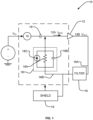
- Figure 1 shows a sensor circuit 10 according to an example embodiment.
- Sensor circuit 10 is designed to detect electrical signals within a frequency band of interest.
- the frequency band of interest includes frequencies above some cut-off frequency.
- the cut-off frequency may be in the milliHertz range (e.g. 100mHz or so).
- the frequency band of interest is 100 mHz to 100Hz, or 1 kHz or so. This frequency band is a frequency band useful in certain EEG applications.
- the precise upper and lower bounds of the frequency band of interest are not critical. Other frequency bands may be of interest in other applications.
- Sensor circuit 10 comprises an amplifier 12 having an input 12A and an output 12B.
- Input 12A is connected to a sensor 14 which may, for example, comprise an electrode in proximity to the skin of a subject. It is unnecessary for the electrode to be in conductive contact with the subject's skin.
- the sensor may comprise a dry electrode or a non-contact electrode, for example.
- Amplifier 12 has a high input impedance to facilitate sensing small changes in electrical potential at the subject's skin notwithstanding the fact that sensor 14 does not make good or even any conductive contact with the subject's skin.
- Amplifier 12 may, for example, comprise a conventional amplifier such as an operational amplifier.
- amplifier 12 comprises an operational amplifier in a unity gain configuration,
- Circuit 10 includes a capacitor 15 between sensor 14 and amplifier 12.
- Capacitor 15 may be provided by capacitance of sensor 14 and/or by a separate component. Providing a capacitor 15 as a separate component provides the added safety advantage of ensuring that circuit 10 cannot supply direct current to the subject unless capacitor 15 fails.
- Circuit 10 includes circuitry for correcting charge imbalances at the input of amplifier 12. Because amplifier 12 has a high input impedance and capacitor 15 also presents a high impedance to direct currents electrical charge can build up at the input of amplifier 12. The charge build up can be caused by the bias current required by amplifier 12 (shown as I BIAS ) which, although it may be tiny (in the range of picoamperes or femtoamperes in some cases) is not zero. Electrostatic discharges can also cause electric charge to build up at the input of amplifier 12.
- I BIAS bias current required by amplifier 12
- Circuit 10 is configured to provide a relatively low-impedance pathway to address charge imbalances at input 12A of amplifier 12 at one or more frequencies outside the frequency band of interest while maintaining a high impedance for all frequencies within the frequency band of interest. This is achieved by the combination of a filter 16 and an impedance 18 connected between an output 16B of filter 16 and the input 12A of amplifier 12. The input 16A to filter 16 is connected to the output 12B of amplifier 12. Impedance 18 comprises a resistor in a simple case. Other cases are described below. The electrical resistance of impedance 18 may be much lower than the input impedance of amplifier 12.
- amplifier 12 may have an input impedance of 10 9 ohms or more while impedance 18 has a resistance on the order of 10 7 ohms or so.
- the exact value for the resistance of impedance 18 is not critical.
- the resistive component of the impedance of impedance 18 is significantly lower than a resistive component of the impedance of the connection between input 12A of amplifier 12 and the subject.
- the resistive component of the impedance of impedance 18 is significantly lower than a resistive component of the impedance of any other connection to the input 12A of amplifier 12.
- the gains of amplifier 12 and filter 18 are selected such that, for signals within the frequency band of interest, the combined gain of amplifier 12 and filter 18 is unity.
- the signal at output 16B of filter 16 is the same as the signal at input 12A of amplifier 12. Therefore, for signals within the frequency band of interest, no current flows through impedance 18 since there is no potential difference across impedance 18.
- Impedance 18 may be called a phantom impedance because, within the frequency band of interest, it is as if impedance 18 is not present.
- the frequency response of filter 16 be relatively flat (constant) across the frequency band of interest. For many applications the frequency response should be flat to within ⁇ .5% across the frequency band of interest or ⁇ .1% in more demanding applications. It is also desirable that the gain of the combination of amplifier 12 and filter 16 be unity to a good level of precision within the frequency band of interest. In some embodiments the combined gain of filter 16 and amplifier 12 is 1 ⁇ .005 or 1 ⁇ 0.001 across a frequency band of interest (which may be, for example, the frequency band or a subset of the frequency band spanning 1 mHz to 1KHz). The required tolerance will depend on the application.
- the combined gain of amplifier 12 and filter 16 is unity to within a factor given by: R 18 ⁇ 2 ⁇ FC 15 where R 18 is the impedance of impedance 18 at the highest frequency, F, in the frequency band of interest, and C 15 is the capacitance of capacitor 15. So, for example, where impedance 18 is provided by a resistor having a resistance of 10 M ⁇ , and capacitor 15 has a value of 0.1 picoFarads and the maximum frequency of interest is 400 Hz then the combined gain of amplifier 12 and filter 16 in such embodiments is unity to within a factor of ⁇ 0.0027.
- amplifier 12 and filter 16 both have a gain of one for signals in the frequency band of interest. This is preferred because there are well known constructions for amplifiers that maintain unity gain despite temperature variations and components that may be somewhat out of tolerance. It is more difficult to design an amplifier that will reliably maintain a particular non-unity gain. Nevertheless, in some alternative embodiments, amplifier 12 has a non-unity gain and filter 16 has a gain that is the inverse of the gain of amplifier 12 within the frequency band of interest.
- amplifier 12 and filter 16 do not introduce a net phase shift in signals within the frequency band of interest.
- relatively low-frequency signals e.g. signals having frequencies less than a few KHz
- designing a filter and amplifier combination that does not materially shift phases of signals in a frequency band of interest is well within the level of routine skill in the art. If, for some reason, it is desired to use an amplifier 12 or filter 16 that may introduce a phase shift then the other one of amplifier 12 and filter 16 may be constructed in a way that introduces an equal and opposite phase shift or one or more additional circuit elements may be introduced to correct the phase shift.
- Filter 16 may have a wide variety of constructions.
- filter 16 is a passive filter.
- filter 16 has active components.
- Filter 16 may be an analog filter or a digital filter.
- Filter 16 may be a high-pass filter or a bandpass filter.
- An example case where filter 16 is an analog filter with passive components is the case where filter 16 is an RC filter or a LRC filter.
- filter 16 is a first-order high pass filter.
- filter 16 may be a second-order or higher-order filter.
- filter 16 has a flat frequency response for frequencies within the frequency band of interest and a frequency response that falls off at least for frequencies below the frequency band of interest.
- filter 16 may comprise a second-order filter having an output that converges toward a fixed electrical potential as the frequency decreases below a lower cut-off frequency. Any DC signal at input 12A of amplifier 12 that has a value that is different from the fixed electrical potential will see a relatively low-impedance path through impedance 18 and will equalize to the fixed electrical potential.
- bias current may be supplied to amplifier 12 and charge imbalances at amplifier input 12A due to static electricity are neutralized while maintaining a high input impedance for signals within the frequency band of interest.
- a signal may be taken from the output of filter 16 or from the output 12B of amplifier 12 for further processing.
- the signal may be conditioned, further filtered, digitized by an analog-to-digital converter etc.
- the signal may be applied in any of a wide range of applications including applications such as monitoring signals present at sensor 14, determining physiological information about a subject by processing the signals, generating feedback signals, and the like.
- shield 19 may include a shield of one or more shielded cables connected to carry signals from sensor 14 to circuit 10. In such embodiments shield 19 is actively maintained at the same potential as the signal being detected for frequencies in the frequency band of interest. This reduces the pickup of electrical noise.
- Shield 19 may be arranged to shield sensor 14 and/or conductors connecting sensor 14 to amplifier 12 and/or amplifier 12 and/or filter 16. In an example embodiment, shield 19 shields a side of sensor 14, input capacitor 15, impedance 18, the input of amplifier 12 and a cable (if present) comprising a conductor connecting sensor 14 to the part of the circuit containing amplifier 12.
- impedance 18 comprises components in addition to a resistor 18A.
- impedance 18 optionally provides a capacitor 18B in parallel to resistor 18A.
- Capacitor 18B may provide some protection against electrostatic discharges and may also provide a reduced-impedance path for high frequency signals.
- impedance 18 may comprise a resistor 18A in parallel with one or more optional electrostatic discharge protection devices (ESDs) such as transient voltage suppression (TVS) diodes, Zener diodes, multilayer varistors, ceramic capacitors, or the like.
- ESDs electrostatic discharge protection devices
- TVS transient voltage suppression
- Zener diodes Zener diodes
- multilayer varistors ceramic capacitors, or the like.
- Electrostatic discharges tend to have very fast rise times (high frequencies). Filter 16 may block such high frequencies such that an electrostatic discharge results in a voltage across impedance 18 which can trigger the operation of an ESD.
- An ESD 18C is illustrated.
- impedance 18 is provided by a discrete resistor 18A.
- impedance 18 is provided by a device that provides an electrical resistance between the output of filter 16 and input 12A of amplifier 12 and also provides other functionality.
- filter 16 is implemented as a digital filter, for example within a digital signal processor (DSP) programmed to provide a variable gain.
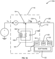
- Figure 1A illustrates an example circuit 10A according to an embodiment in which filter 16 is implemented by a DSP 20 executing software instructions 22.
- the analog output signal V OUT from amplifier 12 is converted to digital format by analog-to-digital converter (ADC) 23.
- ADC analog-to-digital converter
- the digital signal is processed by DSP 20.
- the digital output of DSP 20 is converted to analog by a digital-to-analog converter (DAC) 24 and applied to impedance 18 which operates as described above.
- DAC digital-to-analog converter
- filter 16 has a variable gain within the frequency band of interest.
- the gain of filter 16 may be actively controlled to maintain a gain that is the inverse of the gain of amplifier 12.
- DSP 20 may be configured by software 22 to measure the gain of amplifier 12.
- circuit 10A may be configured to generate a test signal having a known amplitude and a frequency outside of (e.g. just above) the frequency band of interest.
- the test signal may be generated by a separate oscillator or signal generator but it is convenient to program DSP 20 to generate the test signal and to apply the test signal at its output.
- DSP 20 is configured to detect the test signal at the output of amplifier 12 and to determine the gain of amplifier 12 by comparing the initial amplitude of the test signal to the amplitude of the amplified test signal at the output of amplifier 12. DSP 20 may then adjust the gain of filter 16, as and if necessary, to be the inverse of the measured gain of amplifier 12.
- the amplitude of the test signal may be regulated to have a desired known value but this is not mandatory since DSP 20 may optionally be configured to measure the amplitude of the initial test signal 12 using an analog-to-digital converter (ADC).
- ADC analog-to-digital converter
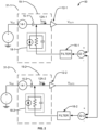
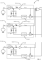
- FIG. 2 shows another example circuit 30 which provides two sensor circuits 31-1 and 31-2 connected in a differential configuration.
- elements that are the same as or similar to elements that are depicted in Figure 1 have the same reference numbers except that the suffixes '-1' and '-2' are added to indicate which sensor circuit (31-1 or 31-2) the element is part of. These suffixes may be omitted when discussing the elements generally.
- Each sensor circuit 31 comprises an amplifier 12, a filter 16 and an impedance 18, all of which may be as described herein.
- Circuits 31-1 and 31-2 differ from circuits 10 and 10A described above in that they each include a difference circuit 32 having inputs connected to receive output signals from amplifiers 12-1 and 12-2 and an output connected to the corresponding filter 16.
- Difference circuits 32 may be implemented in the digital or analog domains. Where filters 16 are implemented digitally it can be convenient to implement difference circuits 32 in the same processor(s) (e.g. DSP) used to implement filters 16.
- a first voltage signal (V IN1 ) is detected at sensor 14-1 and applied at the input of amplifier 12-1 by way of capacitor 15-1.
- a second voltage signal (V IN2 ) is detected at sensor 14-2 and applied at the input of amplifier 12-2 by way of capacitor 15-2.
- output voltages V OUT1 and V OUT2 are respectively presented at outputs of amplifiers 12-1 and 12-2.
- Differential circuit 32-1 determines the difference between V OUT1 and V OUT2 and applies that difference to the input of filter 16-1.
- Differential circuit 32-2 determines the difference between V OUT2 and V OUT1 and applies that difference to the input of filter 16-2.
- V 16-1 is the signal at the output of filter 16-1, V IN1 and V IN2 are as described above, and V AVG is the average of V IN1 and V IN2 .
- the signal at the output of filter 16-2 is given by a similar relationship except that V IN1 and V IN2 are interchanged.
- Difference signals from first and/or second sensor circuits 31-1 and 31-2 may be processed for an intended application.
- the difference signals may be obtained at the output of one of filters 16-1 and 16-2 or one of differential circuits 32-1 and 32-2.
- a separate difference circuit may determine the difference between the outputs of amplifiers 12-1 and 12-2 to yield a difference signal that may be provided to a data processor e.g. a programmable processor such as a DSP, microprocessor, embedded processor or the like or a logic circuit such as a hard-wired logic circuit, custom logic chip (e,g, an ASIC), suitably-configured configurable logic (e.g. a configured field programmable gate array - FPGA), or suitable combinations of these.
- a data processor e.g. a programmable processor such as a DSP, microprocessor, embedded processor or the like or a logic circuit such as a hard-wired logic circuit, custom logic chip (e,g, an ASIC), suitably-configured configurable logic (e.
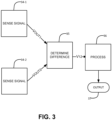
- Figure 3 shows an example case where outputs V OUT1 and V OUT2 respectively obtained at blocks 34-1 and 34-2 by sensing signals using circuits as described herein (e.g. using sensor circuits 31-1 and 31-2) are subtracted at block 35 to yield a difference signal V 12 .
- Block 35 may be implemented using an analog difference circuit or may comprise a numerical subtraction step performed after digitization of V OUT1 and V OUT2 .
- Difference signal V 12 is processed in block 36.
- Block 36 may comprise processing difference signal V 12 according to algorithms implemented in a data processor, logic circuits or the like to produce an output 37.
- output 37 is a feedback signal that is detectable (consciously or sub-consciously) by a human sensory system such as the auditory system or the visual system or the tactile system.
- the output comprises a modulation or other modification to sounds being presented to a subject.
- one or more electrodes for one or more sensors is provided by a layer in a printed circuit board.
- An electrically-conducting shield electrically insulated from the electrode may be provided by another layer of the printed circuit board.
- the shield and electrode may, for example, be separated by a non-conducting layer of the printed circuit board.
- the shield in some embodiments is larger than and overlaps with edges of the electrode.
- a sensor circuit may be provided on the same printed circuit board. In such embodiments the sensor circuit may be connected to the electrode and to a shield, if present, by conductive elements of the printed circuit board.
- the printed circuit board is flexible. In such embodiments the printed circuit board may be flexed to cause a curvature in the electrode that matches a curvature of a portion of a subject such as a person.
- FIG. 4 shows an example circuit 50 comprising a plurality of sensor circuits 51-1, 51-2, ... 51-N. Circuit 50 may include any reasonable number of sensor circuits 51. Each sensor circuit 51 may be similar to sensor circuit 10 or 10A as described above. Circuit 50 differs from the circuits described above in the signals input to filters 16.
- the input to each filter 16 comprises a combination of the output of the corresponding amplifier 12 with a representative signal based on the outputs of one or more other ones of amplifiers 12.
- the representative signal may have a value such as an average, mean or median that is representative of the collective outputs of amplifiers 12.
- the representative signal may be subtracted from the output of the corresponding amplifier 12.
- the output of each amplifier 12 may then be the difference between the corresponding input signal (e.g. V IN1 ) and the representative signal. This may be advantageous in cases where the absolute magnitudes of measured signals are not important but the relationships between the measured signals is what is important.
- a combining circuit may be connected between the output of the amplifier and the input of the filter to generate the signal that is input to the filter.
- the combining circuit comprises a difference (subtraction) circuit. Combining may be performed in the analog or digital domains.
- a difference circuit is configured to subtract from the amplifier output signal a function of the output signals from the additional signal sensors.
- Circuit 50 includes an averaging circuit 55 that corresponds to the second term on the right-hand side of equation (2). Difference circuits 32 in each sensor circuit 51 are connected to subtract the output of averaging circuit 55 from the output of the corresponding amplifier 12. For example, difference circuit 32-1 in sensor circuit 51-1 is connected to subtract the output of averaging circuit 55 from the output of amplifier 12-1.
- Averaging circuit 55 may be implemented as an analog circuit, as a digital process or as a combination thereof.
- each sensor circuit 51 in circuit 50 is indicative of the difference between the signal V IN picked up by that circuit 50 and the representative signal value (e.g. the average output of all of sensor circuits 51).
- circuit 50 provides an output similar to a circuit that provides a ground that is connected to the subject and driven by the representative signal (e.g. to have a potential equal to the average of the sensed signals).
- the representative signal is constructed from the filtered signals (e.g. the signals at the outputs of filters 16) instead of the signals at the outputs of amplifiers 12 as shown in Figure 4 .
- FIG. 5 illustrates an example neurosensing system 60 comprising at least four sensors, 14-1, 14-2, 14-3 and 14-4. Signal sensors 14-1 and 14-2 are connected to a differential sensor circuit 61-1. Signal sensors 14-3 and 14-4 are connected to a differential sensor circuit 61-2.
- Sensor circuit 61-1 is configured to output a difference signal representing the difference between signals picked up by sensors 14-1 and 14-2.
- sensor circuits 61-2 is configured to output a difference signal representing the difference between signals picked up by sensors 14-3 and 14-4.
- Sensors 14-1 and 14-2 may be located to detect signals on one side of a subject's head (e.g. the left side) while sensors 14-3 and 14-4 may be located to detect signals on the other side of the subject's head (e.g. the right side).
- the resulting right and left difference signals 64, 65 are directed to a data processor 66 executing an algorithm that processes the difference signals and generates feedback to be delivered to the subject.
- data processor 66 may analyze signals 64 and 65 to evaluate balance between the subject's left brain activity and right brain activity. Data processor 66 may then issue control signals to an audio controller 67 to modify a sound signal 68 to yield a modified sound signal 69 which may be delivered by audio controller 67 to the subject. For example, audio controller 67 may be controlled to insert audio dropouts into sound signal 68 if there is an imbalance detected between the subject's left-brain and right-brain activity levels.
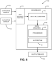
- FIG. 6 shows a system 70 according to another example embodiment.
- System 70 comprises at least two capacitive sensors 72-1 and 72-2 which sense the charge on the skin or scalp of a user.
- a capacitive sensor is a sensor that does not rely on low-impedance electrical conduction to pick up signals from a subject.
- a capacitive sensor provides an electrode that is capacitively coupled to the subject's skin (the scalp in some embodiments). It is possible but not mandatory for the electrode of the capacitive sensor to be electrically insulated from the subject's skin, for example by a layer of a dielectric material.
- Capacitive sensors 72 and 72 are connected to a device 74 which detects and processes signals picked up by capacitive sensors 72.
- Device 74 comprises a high impedance front end 73 that incorporates one or more sensor circuits as described herein
- device 74 comprises an EEG device that includes a data acquisition module 76 and a data analysis module 78, which may be provided by a data processor 80 executing an algorithm 82.
- Data analysis module 78 controls an output device 84.
- Output device 84 may include one or more devices of any of a wide variety of types including output devices such as a display, a printer, a sound generator, a data logger a digital or analog control signal for another device etc.
- the same processor is applied to both: perform digital filtering as described for example with reference to Figure 1A and to process detected signals.
- EEG data are acquired by way of capacitive sensors 72
- information about the brain's performance is calculated by signal processing algorithm 82 in the data analysis module 78.
- Imbalances detected between activity of the right and left sides of the brain of a subject results in signal processing algorithm 82 determining an imbalance, and the processor 80 signaling output device 84 to modify a sound signal being played to the subject (e.g. by inserting one or more auditory drop outs into the sound signal).
- the sound signal comprises a music signal in some embodiments.
- one or more circuits as described herein are mounted to a headset which also supports potential-sensing contacts coupled to inputs of the amplifiers.
- the headset may be worn such that EEG signals detected at the potential-sensing contacts are amplified by amplifiers 12.
- the headset supports at least one first pair of potential-sensing contacts for contacting the left-side of a person's scalp when the headset is being worn and at least one second pair of potential-sensing contacts for contacting the left-side of a person's scalp when the headset is being worn.
- the potential-sensing contacts may comprise electrodes, non-contact sensors, high-impedance sensors or the like. In some embodiments the potential-sensing contacts have DC impedances in excess of 1 M ⁇ or in excess of 10 M ⁇ . In some embodiments the potential-sensing contacts are capacitively coupled to the inputs of corresponding amplifiers 12 (e.g. by capacitors 15).
- Another aspect of the invention provides methods for detecting electrical potentials.
- One aspect comprises coupling an electrical potential to the input of an amplifier, at an output of the amplifier detecting an amplifier output signal comprising a signal of interest; extracting the signal of interest from the amplifier output signal; and applying the extracted signal of interest to one end of an impedance having a second end connected to the amplifier input.
- the signal of interest is a signal within a specified frequency band.
- extracting the signal of interest may comprise filtering the amplifier output signal in a bandpass filter or a low-pass filter.
- the signal of interest comprises a difference between signals representing potentials measured at two locations.
- extracting the signal of interest may comprise subtracting another signal from the amplifier output signal.
- Some embodiments comprise supplying a DC bias current for the amplifier by way of the impedance.
- Amplifiers 12 in the circuits described above can be conveniently provided by integrated operational amplifiers (op amps) although this is not mandatory. Operational amplifiers having very high input impedances and low bias current requirements are commercially available. It is not mandatory that the amplifiers, filters and difference circuits described herein be separate and discrete from one another. These elements may share components. For example, an amplifier may have bandpass characteristics that provide the described filtering function - in which case a separate filter may not be present or required. In embodiments where two amplifiers are shown connected to provide a differential output alternative embodiments may use a single differential amplifier with separate feedback paths for each input.
- the single sensor circuit is implemented with only one amplifier providing that its frequency response is non-unity below the band of interest.
- the amplifier is a differential amplifier then the dual sensor can be implemented without the differential circuit.
- Embodiments of the invention may be implemented using specifically designed hardware, configurable hardware, programmable data processors configured by the provision of software (which may optionally comprise "firmware") capable of executing on the data processors, special purpose computers or data processors that are specifically programmed, configured, or constructed to perform one or more steps in a method as explained in detail herein and/or combinations of two or more of these.
- software which may optionally comprise "firmware”
- specifically designed hardware are: logic circuits, application-specific integrated circuits ("ASICs”), large scale integrated circuits (“LSIs”), very large scale integrated circuits (“VLSIs”), and the like.
- programmable hardware examples include one or more programmable logic devices such as programmable array logic (“PALs”), programmable logic arrays (“PLAs”), and field programmable gate arrays (“FPGAs”)).
- PALs programmable array logic
- PLAs programmable logic arrays
- FPGAs field programmable gate arrays
- programmable data processors are: microprocessors, digital signal processors ("DSPs"), embedded processors, graphics processors, math co-processors, general purpose computers, server computers, computer workstations, and the like.
- DSPs digital signal processors
- embedded processors embedded processors
- graphics processors graphics processors
- math co-processors general purpose computers
- server computers computer workstations
- one or more data processors in a biofeedback device may implement methods as described herein by executing software instructions in a program memory accessible to the processors.
- systems, methods and apparatus have been described herein for purposes of illustration. These are only examples.
- the technology provided herein can be applied to systems other than the example systems described above.
- such systems may be applied to sensing all manner of bioelectric signals.
- Such signals may be applied for example for monitoring function of the brain, heart, and other organs.
- the present technology may be applied in medical devices such as prosthetics, assistive devices, cardiac monitors and myography devices and related methods; sleep and alertness monitoring; game, digital appliance and computer interaction; control of vehicles and equipment; fitness devices which include physiological monitoring functions and so on.
- the technology also has application in sensing signals of non-biological origin.
- Sensing circuits as described herein may be supported by and/or integrated into clothing, headwear, helmets or the like or surfaces that are touched by or adjacent to body parts of persons or animals when in use (such as handles, knobs, surfaces of furniture such as chairs, beds, seats, headrests, medical probes, or the like).
Landscapes
- Health & Medical Sciences (AREA)
- Life Sciences & Earth Sciences (AREA)
- Engineering & Computer Science (AREA)
- Physics & Mathematics (AREA)
- Public Health (AREA)
- Surgery (AREA)
- Veterinary Medicine (AREA)
- General Health & Medical Sciences (AREA)
- Animal Behavior & Ethology (AREA)
- Biophysics (AREA)
- Pathology (AREA)
- Biomedical Technology (AREA)
- Heart & Thoracic Surgery (AREA)
- Medical Informatics (AREA)
- Molecular Biology (AREA)
- Signal Processing (AREA)
- General Physics & Mathematics (AREA)
- Psychiatry (AREA)
- Power Engineering (AREA)
- Computer Vision & Pattern Recognition (AREA)
- Physiology (AREA)
- Artificial Intelligence (AREA)
- Mathematical Physics (AREA)
- Microelectronics & Electronic Packaging (AREA)
- Psychology (AREA)
- Measurement And Recording Of Electrical Phenomena And Electrical Characteristics Of The Living Body (AREA)
Claims (14)
- Vorrichtung (10, 10A, 30, 50) zum Messen elektrischer Potenziale in einem Frequenzband von Interesse, wobei die Vorrichtung (10, 10A, 30, 50) folgende Elemente umfasst:einen Verstärker (12) mit einer ersten Verstärkung, einem Eingang (12A) und einem Ausgang (12B);ein Filter (16) mit einer zweiten Verstärkung, die die Umkehrung der ersten Verstärkung ist, einem Eingang (16A), der so geschaltet ist, dass er ein Signal vom Verstärkerausgang (12B) empfängt, und einem Ausgang (16B); undeine Impedanz (18) mit einer Widerstandskomponente (18A), die zwischen dem Filterausgang (16B) und dem Verstärkereingang (12A) gekoppelt ist;wobei das Filter (16) ein Durchlassband aufweist, das das Frequenzband von Interesse einschließt und Gleichstromsignale ausschließt;dadurch gekennzeichnet, dassder Verstärker (12) und das Filter (16) kombiniert eine Verstärkung von eins für Signale im Frequenzband von Interesse aufweisen;und dass das Frequenzband von Interesse die Frequenzen im Bereich von 1 Hz bis 100 Hz oder 100 mHz bis 300 Hz umfasst.
- Vorrichtung (10, 10A, 30, 50) nach Anspruch 1, wobei die Impedanz (18) einen Kondensator (18B) und/oder eine Schutzvorrichtung (18C) gegen elektrostatische Entladung umfasst, die parallel zu einem Widerstand (18A) geschaltet ist.
- Vorrichtung (10, 10A, 30, 50) nach Anspruch 1, wobei das Filter (16) einen flachen Frequenzgang innerhalb des Frequenzbandes von Interesse aufweist.
- Vorrichtung (10, 10A, 30, 50) nach Anspruch 1, wobei das Filter (16) ein digitales Filter umfasst.
- Vorrichtung (10A) nach Anspruch 4, umfassend einen Analog-Digital-Wandler (23), der so geschaltet ist, dass er das Signal vom Verstärkerausgang (12B) digitalisiert, einen digitalen Signalprozessor (20), der dafür ausgelegt ist, das digitalisierte Signal zum Erhalten eines digitalisierten gefilterten Signals digital zu filtern, und einen Digital-Analog-Wandler (24), der dafür ausgelegt ist, das digitalisierte gefilterte Signal in ein analoges gefiltertes Signal umzuwandeln, wobei der Digital-Analog-Wandler (24) einen Ausgang aufweist, der so gekoppelt ist, dass er das analoge gefilterte Signal über die Impedanz (18) an den Verstärkereingang (12A) anlegt.
- Vorrichtung (10, 10A, 30, 50) nach Anspruch 1, umfassend eine Abschirmung (19) mit niedriger Impedanz, die mit dem Ausgang (16B) des Filters (16) verbunden und so angeordnet ist, dass sie mindestens eines vom Eingang (12A) des Verstärkers (12) und der Impedanz (18) abschirmt.
- Vorrichtung (30, 50) nach Anspruch 1, umfassend eine Kombinationsschaltung (32), die zwischen den Ausgang (12B) des Verstärkers (12) und den Eingang (16A) des Filters (16) geschaltet ist, wobei die Kombinationsschaltung (32) dem Eingang des Filters (16) ein Signal bereitstellt, das ein Verstärkerausgangssignal vom Verstärker (12) und Ausgangssignale von einem oder mehreren zusätzlichen Signalsensoren (14) kombiniert.
- Vorrichtung (30, 50) nach Anspruch 7, wobei die Kombinationsschaltung (32) eine Differenzschaltung (32) umfasst, die so ausgelegt ist, dass sie vom Verstärkerausgangssignal eine Funktion der Ausgangssignale vom einen oder den mehreren zusätzlichen Signalsensoren (14) subtrahiert.
- Vorrichtung (50) nach Anspruch 8, wobei die Funktion der Ausgangssignale vom einen oder den mehreren zusätzlichen Signalsensoren (14) einen Mittelwert (55) umfasst.
- Vorrichtung (30, 50) nach Anspruch 8, wobei der eine oder die mehreren zusätzlichen Signalsensoren (14) umfassen:einen zweiten Verstärker (12) mit einem Eingang (12A) und einem Ausgang (12B);ein zweites Filter (16) mit einem Eingang (16A), der so geschaltet ist, dass er ein Signal von einer zweiten Differenzschaltung (32) empfängt, und einem Ausgang (16B) ;eine zweite Impedanz (18) mit einerWiderstandskomponente (18A), die zwischen dem zweiten Filterausgang (16B9) und dem zweiten Verstärkereingang (12A) gekoppelt ist;wobei die Funktion der Ausgangssignale von den zusätzlichen Signalsensoren (14) ein zweites Verstärkerausgangssignal vom zweiten Verstärker (12) umfasst; undwobei die zweite Differenzschaltung (32) so geschaltet ist, dass sie vom zweiten Verstärkerausgangssignal das Verstärkerausgangssignal subtrahiert.
- Neurofeedback-System (60, 70), umfassend:mehrere Sensorschaltungen, die jeweils eine Vorrichtung (10, 10A, 30, 50) nach einem der Ansprüche 1 bis 9 mit einem kapazitiven Sensor (14) umfassen, der mit dem Eingang (12A) des Verstärkers (12) verbunden ist;einen Prozessor (66, 80), der so geschaltet ist, dass er Signale von den Ausgängen (12B) der Verstärker (12) der Schaltungen empfängt und verarbeitet; undein Neurofeedback-Modul (67, 84), das dafür ausgelegt ist, eine sensorische Ausgabe bereitzustellen.
- Neurofeedback-System (60, 70) nach Anspruch 11, wobei die mehreren Sensorschaltungen an einem Headset montiert sind, die kapazitiven Sensoren (14) vom Headset getragen werden und jede der mehreren Sensorschaltungen eine Differenzschaltung (32) umfasst, die zwischen den Ausgang (12B) des Verstärkers (12) und das Filter (16) geschaltet ist, und die Differenzschaltungen (32) dafür ausgelegt sind, vom Verstärkerausgangssignal ein Signal zu subtrahieren, das auf den Ausgangssignalen von einer oder mehreren anderen der Sensorschaltungen (14) basiert.
- Verfahren zum Erfassen elektrischer Potenziale, umfassend:Erfassen eines Verstärkerausgangssignals, das ein Signal von Interesse an einem Ausgang (12B) eines Verstärkers (12) mit einer ersten Verstärkung und einem mit einem elektrischen Potenzial gekoppelten Eingang (12A) umfasst;Extrahieren des Signals von Interesse aus dem Verstärkerausgangssignal, wobei der Schritt des Extrahierens des Signals von Interesse das Filtern des Verstärkerausgangssignals unter Verwendung eines Filters (16) mit einer zweiten Verstärkung, die die Umkehrung der ersten Verstärkung ist, und einem Durchlassband, das Gleichstromsignale ausschließt, umfasst, und wobei der Verstärker (12) und das Filter (16) kombiniert eine Verstärkung von eins für Signale in einem Frequenzband aufweisen, das Frequenzen im Bereich von 1 Hz bis 100 Hz oder 100 mHz bis 300 Hz innerhalb des Durchlassbandes des Filters (16) umfasst; undAnlegen des extrahierten Signals von Interesse an ein Ende einer Impedanz (18) mit einem zweiten Ende, das mit dem Verstärkereingang (12A) verbunden ist.
- Verfahren nach Anspruch 13, wobei das Signal von Interesse eine Differenz zwischen Signalen umfasst, die an zwei Stellen gemessene Potenziale repräsentieren, und das Extrahieren des Signals von Interesse das Filtern eines Differenzsignals umfasst, wobei das Differenzsignal durch Subtrahieren eines anderen Signals vom Verstärkerausgangssignal erzeugt wird.
Applications Claiming Priority (2)
| Application Number | Priority Date | Filing Date | Title |
|---|---|---|---|
| US201361910033P | 2013-11-27 | 2013-11-27 | |
| PCT/CA2014/051133 WO2015077886A1 (en) | 2013-11-27 | 2014-11-26 | Ultra high impedance sensor with applications in neurosensing |
Publications (4)
| Publication Number | Publication Date |
|---|---|
| EP3074778A1 EP3074778A1 (de) | 2016-10-05 |
| EP3074778A4 EP3074778A4 (de) | 2017-08-30 |
| EP3074778C0 EP3074778C0 (de) | 2024-01-24 |
| EP3074778B1 true EP3074778B1 (de) | 2024-01-24 |
Family
ID=53198152
Family Applications (1)
| Application Number | Title | Priority Date | Filing Date |
|---|---|---|---|
| EP14865209.2A Active EP3074778B1 (de) | 2013-11-27 | 2014-11-26 | Sensor mit ultrahoher impedanz für neurowahrnehmung |
Country Status (7)
| Country | Link |
|---|---|
| US (1) | US10660575B2 (de) |
| EP (1) | EP3074778B1 (de) |
| JP (1) | JP6659536B2 (de) |
| CN (1) | CN105814443B (de) |
| AU (1) | AU2014357320B2 (de) |
| CA (1) | CA2928141C (de) |
| WO (1) | WO2015077886A1 (de) |
Families Citing this family (20)
| Publication number | Priority date | Publication date | Assignee | Title |
|---|---|---|---|---|
| KR102015716B1 (ko) * | 2014-12-19 | 2019-08-28 | 티앤더블유 엔지니어링 에이/에스 | 초퍼 변조를 이용한 폐-루프 단위-이득 증폭기를 가지는 능동 전극 |
| US10765363B2 (en) * | 2016-09-30 | 2020-09-08 | Cognionics, Inc. | Headgear for dry electroencephalogram sensors |
| EP3428659A1 (de) * | 2017-07-12 | 2019-01-16 | LEM Intellectual Property SA | Kontaktloser spannungswandler |
| EP3684463B1 (de) | 2017-09-19 | 2025-05-14 | Neuroenhancement Lab, LLC | Verfahren und vorrichtung für neuro-enhancement |
| US11717686B2 (en) | 2017-12-04 | 2023-08-08 | Neuroenhancement Lab, LLC | Method and apparatus for neuroenhancement to facilitate learning and performance |
| US12280219B2 (en) | 2017-12-31 | 2025-04-22 | NeuroLight, Inc. | Method and apparatus for neuroenhancement to enhance emotional response |
| US11478603B2 (en) | 2017-12-31 | 2022-10-25 | Neuroenhancement Lab, LLC | Method and apparatus for neuroenhancement to enhance emotional response |
| CN108392254A (zh) * | 2018-04-12 | 2018-08-14 | 上海埃斯埃医械塑料制品有限公司 | 智能腰椎穿刺针 |
| US11364361B2 (en) | 2018-04-20 | 2022-06-21 | Neuroenhancement Lab, LLC | System and method for inducing sleep by transplanting mental states |
| WO2020010320A1 (en) | 2018-07-05 | 2020-01-09 | The Platypus Institute, Inc. | Identifying and strengthening physiological/neurophysiological states predictive of superior performance |
| CN113382683A (zh) | 2018-09-14 | 2021-09-10 | 纽罗因恒思蒙特实验有限责任公司 | 改善睡眠的系统和方法 |
| CA3120321A1 (en) * | 2018-11-28 | 2020-06-04 | Easyg Llc | Contactless electrode for sensing physiological electrical activity |
| CN109464745B (zh) * | 2018-12-25 | 2024-02-13 | 东莞晋杨电子有限公司 | 一种基于生物负反馈的新型脉冲治疗装置 |
| US11786694B2 (en) | 2019-05-24 | 2023-10-17 | NeuroLight, Inc. | Device, method, and app for facilitating sleep |
| US11950934B1 (en) | 2019-06-21 | 2024-04-09 | Verily Life Sciences Llc | Input boosting for chopped neural recording systems |
| US12549134B2 (en) * | 2020-09-22 | 2026-02-10 | Case Western Reserve University | Non-contact sensing node, systems and methods of remote sensing |
| CN113662637B (zh) * | 2021-08-09 | 2024-02-09 | 上海埃斯埃医疗技术有限公司 | 一种智能穿刺针 |
| KR20230101166A (ko) | 2021-12-29 | 2023-07-06 | 삼성전자주식회사 | 뇌신경 신호의 리코딩을 위한 전류 자극기 및 전류 자극기의 동작 방법 |
| CN114916941B (zh) * | 2022-04-07 | 2025-07-29 | 深圳德力凯医疗电子股份有限公司 | 脑电检测装置、阻抗检测方法和存储介质 |
| US20250068239A1 (en) * | 2023-08-24 | 2025-02-27 | Apple Inc. | Gain adjustment using contact detection |
Family Cites Families (28)
| Publication number | Priority date | Publication date | Assignee | Title |
|---|---|---|---|---|
| US827107A (en) | 1905-12-06 | 1906-07-31 | Elonzo Able Maynard | Engine. |
| US4411273A (en) | 1978-01-30 | 1983-10-25 | Roy John E | System and method for electrode pair derivations in electroencephalography |
| DE3143831A1 (de) * | 1981-11-05 | 1983-05-11 | Honeywell and Philips Medical Electronics B.V., 5611 Eindhoven | Ekg-verstaerkerschaltung |
| US4503860A (en) | 1983-03-31 | 1985-03-12 | Bio-Scan, Inc. | Electroencephalography electrode assembly |
| US5230346A (en) | 1992-02-04 | 1993-07-27 | The Regents Of The University Of California | Diagnosing brain conditions by quantitative electroencephalography |
| DE69331441D1 (de) * | 1992-09-03 | 2002-02-14 | Emtee Associates L P | Vorrichtung und verfahren zur rückkopplung von elektroenzaphalographie-signalen |
| US7088175B2 (en) * | 2001-02-13 | 2006-08-08 | Quantum Applied Science & Research, Inc. | Low noise, electric field sensor |
| GB0129390D0 (en) | 2001-12-07 | 2002-01-30 | Clark Terrence D | Electrodynamic sensors and applications thereof |
| US20040155702A1 (en) * | 2003-02-11 | 2004-08-12 | Siemens Elema Ab | Active filter circuit arrangement |
| KR20050072965A (ko) | 2004-01-08 | 2005-07-13 | 림스테크널러지주식회사 | 생체신호 검출용 건식 능동 센서모듈 |
| US7729740B2 (en) | 2004-04-15 | 2010-06-01 | Los Alamos National Security, Llc | Noise cancellation in magnetoencephalography and electroencephalography with isolated reference sensors |
| DE102004063249A1 (de) | 2004-12-23 | 2006-07-13 | Fraunhofer-Gesellschaft zur Förderung der angewandten Forschung e.V. | Sensorsystem und Verfahren zur kapazitiven Messung elektromagnetischer Signale biologischen Ursprungs |
| GB0605717D0 (en) | 2006-03-21 | 2006-05-03 | Univ Sussex | Electric potential sensor |
| US8200317B2 (en) * | 2006-06-30 | 2012-06-12 | Intel Corporation | Method and apparatus for amplifying multiple signals using a single multiplexed amplifier channel with software controlled AC response |
| JP5450436B2 (ja) | 2007-11-28 | 2014-03-26 | ザ リージェンツ オブ ザ ユニバーシティ オブ カリフォルニア | 非接触型生体電位センサ |
| JP5386511B2 (ja) | 2008-02-13 | 2014-01-15 | ニューロスカイ インコーポレイテッド | 生体信号センサを備えたオーディオヘッドセット |
| KR101031799B1 (ko) * | 2009-05-28 | 2011-04-29 | 주식회사 바우압텍 | 정전기 방전 보호 소자 |
| US10987015B2 (en) | 2009-08-24 | 2021-04-27 | Nielsen Consumer Llc | Dry electrodes for electroencephalography |
| CN102025137B (zh) * | 2009-09-21 | 2013-08-21 | 群康科技(深圳)有限公司 | 静电放电保护电路及具有静电放电保护电路的电子装置 |
| US20110282231A1 (en) | 2010-05-12 | 2011-11-17 | Neurofocus, Inc. | Mechanisms for collecting electroencephalography data |
| WO2011146482A1 (en) | 2010-05-18 | 2011-11-24 | Zoll Medical Corporation | Wearable ambulatory medical device with multiple sensing electrodes |
| EP2442443B8 (de) * | 2010-10-15 | 2018-02-07 | IMEC vzw | Erfassungssystem für Mehrkanal-Biopotenzsignal |
| KR101227413B1 (ko) | 2011-03-08 | 2013-02-12 | (주)락싸 | 전기적 비접촉식 생체 신호 측정 장치 및 그 방법 |
| US8780512B2 (en) | 2011-04-01 | 2014-07-15 | Neurosky, Inc. | Low leakage ESD structure for non-contact bio-signal sensors |
| US20120265080A1 (en) | 2011-04-15 | 2012-10-18 | Xiong Yu | Non-contact sensing of physiological signals |
| US8676230B2 (en) | 2011-05-16 | 2014-03-18 | Neurosky, Inc. | Bio signal based mobile device applications |
| US20130079659A1 (en) | 2011-09-23 | 2013-03-28 | Elshan Akhadov | INTEGRATION OF ELECTROENCEPHALOGRAPHY (EEG) AND TRANSCRANIAL DIRECT CURRENT STIMULATION (tDCS) WITH HIGH-SPEED OPERATION, ELECTRODE, RE-USE, AUTOMATED tDCS ELECTRODE CONFIGURATION, AND MULTIPLE INDEPENDENT tDCS CURENT SOURCES |
| KR101308540B1 (ko) * | 2012-02-14 | 2013-09-23 | 서울대학교산학협력단 | 폴리머 폼이 형성된 용량성 전극을 이용한 뇌파 및 전기 생체신호 측정 장치 및 시스템 |
-
2014
- 2014-11-26 WO PCT/CA2014/051133 patent/WO2015077886A1/en not_active Ceased
- 2014-11-26 US US15/031,229 patent/US10660575B2/en active Active
- 2014-11-26 AU AU2014357320A patent/AU2014357320B2/en active Active
- 2014-11-26 CA CA2928141A patent/CA2928141C/en active Active
- 2014-11-26 EP EP14865209.2A patent/EP3074778B1/de active Active
- 2014-11-26 JP JP2016528152A patent/JP6659536B2/ja active Active
- 2014-11-26 CN CN201480062447.XA patent/CN105814443B/zh active Active
Also Published As
| Publication number | Publication date |
|---|---|
| EP3074778A1 (de) | 2016-10-05 |
| EP3074778C0 (de) | 2024-01-24 |
| CN105814443B (zh) | 2020-09-08 |
| EP3074778A4 (de) | 2017-08-30 |
| JP6659536B2 (ja) | 2020-03-04 |
| AU2014357320A1 (en) | 2016-06-02 |
| WO2015077886A1 (en) | 2015-06-04 |
| CA2928141C (en) | 2025-09-16 |
| CN105814443A (zh) | 2016-07-27 |
| US10660575B2 (en) | 2020-05-26 |
| CA2928141A1 (en) | 2015-06-04 |
| AU2014357320B2 (en) | 2019-08-15 |
| JP2016538036A (ja) | 2016-12-08 |
| US20160262703A1 (en) | 2016-09-15 |
Similar Documents
| Publication | Publication Date | Title |
|---|---|---|
| EP3074778B1 (de) | Sensor mit ultrahoher impedanz für neurowahrnehmung | |
| KR101227413B1 (ko) | 전기적 비접촉식 생체 신호 측정 장치 및 그 방법 | |
| Neuman et al. | Biopotential amplifiers | |
| EP2429390B1 (de) | System und verfahren mit flexiblen kapazitiven elektroden zur messung von biosignalen | |
| Scheer et al. | The influence of amplifier, interface and biological noise on signal quality in high-resolution EEG recordings | |
| Dabbaghian et al. | A 9.2-g fully-flexible wireless ambulatory EEG monitoring and diagnostics headband with analog motion artifact detection and compensation | |
| US20160157777A1 (en) | Headset for bio-signals acquisition | |
| EP2394571B1 (de) | Vorrichtung und Verfahren zum Messen eines biologischen Signals | |
| EP2843833B1 (de) | Rekonfigurierbare Messvorrichtung und Verfahren zur Steuerung der Vorrichtung | |
| US20120065536A1 (en) | System and method for neurological evaluation | |
| CN109171702A (zh) | 一种非接触式心电信号的测量装置和测量方法 | |
| JP7039002B2 (ja) | ウェアラブル生体センサ及びノイズキャンセル回路 | |
| US20210267524A1 (en) | Contactless electrode for sensing physiological electrical activity | |
| KR20150017928A (ko) | 공통모드에 의한 차폐 구동을 통해 생체 신호를 측정하는 방법, 장치 및 회로 | |
| KR101308540B1 (ko) | 폴리머 폼이 형성된 용량성 전극을 이용한 뇌파 및 전기 생체신호 측정 장치 및 시스템 | |
| Ding et al. | A novel front-end design for bioelectrical signal wearable acquisition | |
| Su et al. | Noncontact ECG monitoring by capacitive coupling of textiles in a chair | |
| Jamaluddin et al. | Flexible bio-signals channels acquisition system for ECG and EMG application | |
| Fauzani et al. | Two electrodes system: Performance on ECG FECG and EMG detection | |
| Qin et al. | A wireless universal brain-machine interface (bmi) system for epileptic diseases | |
| Ghapanchizadeh et al. | Developing multichannel surface EMG acquisition system by using instrument opamp INA2141 | |
| KR101041943B1 (ko) | 전기적 비접촉 심전도를 이용한 체표전위 측정장치 | |
| Vijayashanthi et al. | An Enhanced Implementation Method for a Single Channel Portable EEG System on Brain Monitoring Applications Using Notch Filters | |
| JP6731435B2 (ja) | 生体信号検出モジュール | |
| Martín Martín | Preprocessing of EMG Signals |
Legal Events
| Date | Code | Title | Description |
|---|---|---|---|
| PUAI | Public reference made under article 153(3) epc to a published international application that has entered the european phase |
Free format text: ORIGINAL CODE: 0009012 |
|
| 17P | Request for examination filed |
Effective date: 20160627 |
|
| AK | Designated contracting states |
Kind code of ref document: A1 Designated state(s): AL AT BE BG CH CY CZ DE DK EE ES FI FR GB GR HR HU IE IS IT LI LT LU LV MC MK MT NL NO PL PT RO RS SE SI SK SM TR |
|
| AX | Request for extension of the european patent |
Extension state: BA ME |
|
| DAX | Request for extension of the european patent (deleted) | ||
| RIC1 | Information provided on ipc code assigned before grant |
Ipc: A61B 5/0488 20060101ALI20170720BHEP Ipc: G01R 19/00 20060101ALI20170720BHEP Ipc: G01R 23/165 20060101ALI20170720BHEP Ipc: G01R 23/167 20060101ALI20170720BHEP Ipc: A61B 5/04 20060101ALI20170720BHEP Ipc: A61B 5/0482 20060101ALI20170720BHEP Ipc: H03F 1/56 20060101ALI20170720BHEP Ipc: A61B 5/0428 20060101AFI20170720BHEP |
|
| A4 | Supplementary search report drawn up and despatched |
Effective date: 20170728 |
|
| STAA | Information on the status of an ep patent application or granted ep patent |
Free format text: STATUS: EXAMINATION IS IN PROGRESS |
|
| 17Q | First examination report despatched |
Effective date: 20210927 |
|
| REG | Reference to a national code |
Ref country code: DE Ref legal event code: R079 Free format text: PREVIOUS MAIN CLASS: G01R0019000000 Ipc: A61B0005050000 Ref country code: DE Ref legal event code: R079 Ref document number: 602014089400 Country of ref document: DE Free format text: PREVIOUS MAIN CLASS: G01R0019000000 Ipc: A61B0005050000 |
|
| RIC1 | Information provided on ipc code assigned before grant |
Ipc: G01R 19/00 20060101ALI20230705BHEP Ipc: G01R 23/167 20060101ALI20230705BHEP Ipc: G01R 23/165 20060101ALI20230705BHEP Ipc: H03F 1/56 20060101ALI20230705BHEP Ipc: A61B 5/05 20060101AFI20230705BHEP |
|
| GRAP | Despatch of communication of intention to grant a patent |
Free format text: ORIGINAL CODE: EPIDOSNIGR1 |
|
| STAA | Information on the status of an ep patent application or granted ep patent |
Free format text: STATUS: GRANT OF PATENT IS INTENDED |
|
| INTG | Intention to grant announced |
Effective date: 20230816 |
|
| GRAS | Grant fee paid |
Free format text: ORIGINAL CODE: EPIDOSNIGR3 |
|
| GRAA | (expected) grant |
Free format text: ORIGINAL CODE: 0009210 |
|
| STAA | Information on the status of an ep patent application or granted ep patent |
Free format text: STATUS: THE PATENT HAS BEEN GRANTED |
|
| AK | Designated contracting states |
Kind code of ref document: B1 Designated state(s): AL AT BE BG CH CY CZ DE DK EE ES FI FR GB GR HR HU IE IS IT LI LT LU LV MC MK MT NL NO PL PT RO RS SE SI SK SM TR |
|
| REG | Reference to a national code |
Ref country code: GB Ref legal event code: FG4D |
|
| REG | Reference to a national code |
Ref country code: CH Ref legal event code: EP |
|
| REG | Reference to a national code |
Ref country code: DE Ref legal event code: R096 Ref document number: 602014089400 Country of ref document: DE |
|
| REG | Reference to a national code |
Ref country code: IE Ref legal event code: FG4D |
|
| U01 | Request for unitary effect filed |
Effective date: 20240223 |
|
| U07 | Unitary effect registered |
Designated state(s): AT BE BG DE DK EE FI FR IT LT LU LV MT NL PT SE SI Effective date: 20240301 |
|
| REG | Reference to a national code |
Ref country code: LT Ref legal event code: MG9D |
|
| PG25 | Lapsed in a contracting state [announced via postgrant information from national office to epo] |
Ref country code: IS Free format text: LAPSE BECAUSE OF FAILURE TO SUBMIT A TRANSLATION OF THE DESCRIPTION OR TO PAY THE FEE WITHIN THE PRESCRIBED TIME-LIMIT Effective date: 20240524 |
|
| PG25 | Lapsed in a contracting state [announced via postgrant information from national office to epo] |
Ref country code: GR Free format text: LAPSE BECAUSE OF FAILURE TO SUBMIT A TRANSLATION OF THE DESCRIPTION OR TO PAY THE FEE WITHIN THE PRESCRIBED TIME-LIMIT Effective date: 20240425 |
|
| PG25 | Lapsed in a contracting state [announced via postgrant information from national office to epo] |
Ref country code: RS Free format text: LAPSE BECAUSE OF FAILURE TO SUBMIT A TRANSLATION OF THE DESCRIPTION OR TO PAY THE FEE WITHIN THE PRESCRIBED TIME-LIMIT Effective date: 20240424 Ref country code: HR Free format text: LAPSE BECAUSE OF FAILURE TO SUBMIT A TRANSLATION OF THE DESCRIPTION OR TO PAY THE FEE WITHIN THE PRESCRIBED TIME-LIMIT Effective date: 20240124 |
|
| PG25 | Lapsed in a contracting state [announced via postgrant information from national office to epo] |
Ref country code: ES Free format text: LAPSE BECAUSE OF FAILURE TO SUBMIT A TRANSLATION OF THE DESCRIPTION OR TO PAY THE FEE WITHIN THE PRESCRIBED TIME-LIMIT Effective date: 20240124 |
|
| PG25 | Lapsed in a contracting state [announced via postgrant information from national office to epo] |
Ref country code: RS Free format text: LAPSE BECAUSE OF FAILURE TO SUBMIT A TRANSLATION OF THE DESCRIPTION OR TO PAY THE FEE WITHIN THE PRESCRIBED TIME-LIMIT Effective date: 20240424 Ref country code: NO Free format text: LAPSE BECAUSE OF FAILURE TO SUBMIT A TRANSLATION OF THE DESCRIPTION OR TO PAY THE FEE WITHIN THE PRESCRIBED TIME-LIMIT Effective date: 20240424 Ref country code: IS Free format text: LAPSE BECAUSE OF FAILURE TO SUBMIT A TRANSLATION OF THE DESCRIPTION OR TO PAY THE FEE WITHIN THE PRESCRIBED TIME-LIMIT Effective date: 20240524 Ref country code: HR Free format text: LAPSE BECAUSE OF FAILURE TO SUBMIT A TRANSLATION OF THE DESCRIPTION OR TO PAY THE FEE WITHIN THE PRESCRIBED TIME-LIMIT Effective date: 20240124 Ref country code: GR Free format text: LAPSE BECAUSE OF FAILURE TO SUBMIT A TRANSLATION OF THE DESCRIPTION OR TO PAY THE FEE WITHIN THE PRESCRIBED TIME-LIMIT Effective date: 20240425 Ref country code: ES Free format text: LAPSE BECAUSE OF FAILURE TO SUBMIT A TRANSLATION OF THE DESCRIPTION OR TO PAY THE FEE WITHIN THE PRESCRIBED TIME-LIMIT Effective date: 20240124 |
|
| PG25 | Lapsed in a contracting state [announced via postgrant information from national office to epo] |
Ref country code: PL Free format text: LAPSE BECAUSE OF FAILURE TO SUBMIT A TRANSLATION OF THE DESCRIPTION OR TO PAY THE FEE WITHIN THE PRESCRIBED TIME-LIMIT Effective date: 20240124 |
|
| PG25 | Lapsed in a contracting state [announced via postgrant information from national office to epo] |
Ref country code: PL Free format text: LAPSE BECAUSE OF FAILURE TO SUBMIT A TRANSLATION OF THE DESCRIPTION OR TO PAY THE FEE WITHIN THE PRESCRIBED TIME-LIMIT Effective date: 20240124 |
|
| PG25 | Lapsed in a contracting state [announced via postgrant information from national office to epo] |
Ref country code: SM Free format text: LAPSE BECAUSE OF FAILURE TO SUBMIT A TRANSLATION OF THE DESCRIPTION OR TO PAY THE FEE WITHIN THE PRESCRIBED TIME-LIMIT Effective date: 20240124 |
|
| PG25 | Lapsed in a contracting state [announced via postgrant information from national office to epo] |
Ref country code: CZ Free format text: LAPSE BECAUSE OF FAILURE TO SUBMIT A TRANSLATION OF THE DESCRIPTION OR TO PAY THE FEE WITHIN THE PRESCRIBED TIME-LIMIT Effective date: 20240124 |
|
| REG | Reference to a national code |
Ref country code: DE Ref legal event code: R097 Ref document number: 602014089400 Country of ref document: DE |
|
| PG25 | Lapsed in a contracting state [announced via postgrant information from national office to epo] |
Ref country code: SK Free format text: LAPSE BECAUSE OF FAILURE TO SUBMIT A TRANSLATION OF THE DESCRIPTION OR TO PAY THE FEE WITHIN THE PRESCRIBED TIME-LIMIT Effective date: 20240124 |
|
| PG25 | Lapsed in a contracting state [announced via postgrant information from national office to epo] |
Ref country code: SM Free format text: LAPSE BECAUSE OF FAILURE TO SUBMIT A TRANSLATION OF THE DESCRIPTION OR TO PAY THE FEE WITHIN THE PRESCRIBED TIME-LIMIT Effective date: 20240124 Ref country code: SK Free format text: LAPSE BECAUSE OF FAILURE TO SUBMIT A TRANSLATION OF THE DESCRIPTION OR TO PAY THE FEE WITHIN THE PRESCRIBED TIME-LIMIT Effective date: 20240124 Ref country code: RO Free format text: LAPSE BECAUSE OF FAILURE TO SUBMIT A TRANSLATION OF THE DESCRIPTION OR TO PAY THE FEE WITHIN THE PRESCRIBED TIME-LIMIT Effective date: 20240124 Ref country code: CZ Free format text: LAPSE BECAUSE OF FAILURE TO SUBMIT A TRANSLATION OF THE DESCRIPTION OR TO PAY THE FEE WITHIN THE PRESCRIBED TIME-LIMIT Effective date: 20240124 |
|
| PLBE | No opposition filed within time limit |
Free format text: ORIGINAL CODE: 0009261 |
|
| STAA | Information on the status of an ep patent application or granted ep patent |
Free format text: STATUS: NO OPPOSITION FILED WITHIN TIME LIMIT |
|
| 26N | No opposition filed |
Effective date: 20241025 |
|
| U20 | Renewal fee for the european patent with unitary effect paid |
Year of fee payment: 11 Effective date: 20241127 |
|
| PGFP | Annual fee paid to national office [announced via postgrant information from national office to epo] |
Ref country code: GB Payment date: 20241127 Year of fee payment: 11 |
|
| PGFP | Annual fee paid to national office [announced via postgrant information from national office to epo] |
Ref country code: CH Payment date: 20241201 Year of fee payment: 11 |
|
| PG25 | Lapsed in a contracting state [announced via postgrant information from national office to epo] |
Ref country code: MC Free format text: LAPSE BECAUSE OF FAILURE TO SUBMIT A TRANSLATION OF THE DESCRIPTION OR TO PAY THE FEE WITHIN THE PRESCRIBED TIME-LIMIT Effective date: 20240124 |
|
| PG25 | Lapsed in a contracting state [announced via postgrant information from national office to epo] |
Ref country code: IE Free format text: LAPSE BECAUSE OF NON-PAYMENT OF DUE FEES Effective date: 20241126 |
|
| PG25 | Lapsed in a contracting state [announced via postgrant information from national office to epo] |
Ref country code: HU Free format text: LAPSE BECAUSE OF FAILURE TO SUBMIT A TRANSLATION OF THE DESCRIPTION OR TO PAY THE FEE WITHIN THE PRESCRIBED TIME-LIMIT; INVALID AB INITIO Effective date: 20141126 |
|
| PG25 | Lapsed in a contracting state [announced via postgrant information from national office to epo] |
Ref country code: CY Free format text: LAPSE BECAUSE OF FAILURE TO SUBMIT A TRANSLATION OF THE DESCRIPTION OR TO PAY THE FEE WITHIN THE PRESCRIBED TIME-LIMIT; INVALID AB INITIO Effective date: 20141126 |