EP3073603A1 - Balance correction device and electricity storage device - Google Patents
Balance correction device and electricity storage device Download PDFInfo
- Publication number
- EP3073603A1 EP3073603A1 EP14862080.0A EP14862080A EP3073603A1 EP 3073603 A1 EP3073603 A1 EP 3073603A1 EP 14862080 A EP14862080 A EP 14862080A EP 3073603 A1 EP3073603 A1 EP 3073603A1
- Authority
- EP
- European Patent Office
- Prior art keywords
- balance correction
- power storage
- timing signal
- circuit
- control
- Prior art date
- Legal status (The legal status is an assumption and is not a legal conclusion. Google has not performed a legal analysis and makes no representation as to the accuracy of the status listed.)
- Granted
Links
- 238000012937 correction Methods 0.000 title claims abstract description 165
- 238000003860 storage Methods 0.000 title claims description 36
- 230000005611 electricity Effects 0.000 title description 2
- 210000000352 storage cell Anatomy 0.000 claims abstract description 158
- 230000007246 mechanism Effects 0.000 description 10
- 230000001360 synchronised effect Effects 0.000 description 10
- 238000005259 measurement Methods 0.000 description 4
- 238000010586 diagram Methods 0.000 description 3
- 238000000034 method Methods 0.000 description 3
- HBBGRARXTFLTSG-UHFFFAOYSA-N Lithium ion Chemical compound [Li+] HBBGRARXTFLTSG-UHFFFAOYSA-N 0.000 description 2
- 230000002159 abnormal effect Effects 0.000 description 2
- 230000005856 abnormality Effects 0.000 description 2
- 210000004027 cell Anatomy 0.000 description 2
- 229910001416 lithium ion Inorganic materials 0.000 description 2
- 230000010355 oscillation Effects 0.000 description 2
- 238000012545 processing Methods 0.000 description 2
- 230000008929 regeneration Effects 0.000 description 2
- 238000011069 regeneration method Methods 0.000 description 2
- 230000002040 relaxant effect Effects 0.000 description 2
- 239000007787 solid Substances 0.000 description 2
- 230000008901 benefit Effects 0.000 description 1
- 239000003990 capacitor Substances 0.000 description 1
- 239000000470 constituent Substances 0.000 description 1
- 230000006866 deterioration Effects 0.000 description 1
- 238000007599 discharging Methods 0.000 description 1
- 230000000694 effects Effects 0.000 description 1
- 230000005669 field effect Effects 0.000 description 1
- 230000006870 function Effects 0.000 description 1
- 238000004519 manufacturing process Methods 0.000 description 1
- 238000012986 modification Methods 0.000 description 1
- 230000004048 modification Effects 0.000 description 1
- 238000012544 monitoring process Methods 0.000 description 1
- 229920000642 polymer Polymers 0.000 description 1
- 230000009467 reduction Effects 0.000 description 1
- 239000004065 semiconductor Substances 0.000 description 1
- 238000004904 shortening Methods 0.000 description 1
- 230000007704 transition Effects 0.000 description 1
Images


Classifications
-
- H—ELECTRICITY
- H02—GENERATION; CONVERSION OR DISTRIBUTION OF ELECTRIC POWER
- H02J—CIRCUIT ARRANGEMENTS OR SYSTEMS FOR SUPPLYING OR DISTRIBUTING ELECTRIC POWER; SYSTEMS FOR STORING ELECTRIC ENERGY
- H02J7/00—Circuit arrangements for charging or depolarising batteries or for supplying loads from batteries
- H02J7/0013—Circuit arrangements for charging or depolarising batteries or for supplying loads from batteries acting upon several batteries simultaneously or sequentially
- H02J7/0014—Circuits for equalisation of charge between batteries
- H02J7/0019—Circuits for equalisation of charge between batteries using switched or multiplexed charge circuits
-
- B—PERFORMING OPERATIONS; TRANSPORTING
- B60—VEHICLES IN GENERAL
- B60L—PROPULSION OF ELECTRICALLY-PROPELLED VEHICLES; SUPPLYING ELECTRIC POWER FOR AUXILIARY EQUIPMENT OF ELECTRICALLY-PROPELLED VEHICLES; ELECTRODYNAMIC BRAKE SYSTEMS FOR VEHICLES IN GENERAL; MAGNETIC SUSPENSION OR LEVITATION FOR VEHICLES; MONITORING OPERATING VARIABLES OF ELECTRICALLY-PROPELLED VEHICLES; ELECTRIC SAFETY DEVICES FOR ELECTRICALLY-PROPELLED VEHICLES
- B60L58/00—Methods or circuit arrangements for monitoring or controlling batteries or fuel cells, specially adapted for electric vehicles
- B60L58/10—Methods or circuit arrangements for monitoring or controlling batteries or fuel cells, specially adapted for electric vehicles for monitoring or controlling batteries
- B60L58/18—Methods or circuit arrangements for monitoring or controlling batteries or fuel cells, specially adapted for electric vehicles for monitoring or controlling batteries of two or more battery modules
- B60L58/22—Balancing the charge of battery modules
-
- B—PERFORMING OPERATIONS; TRANSPORTING
- B60—VEHICLES IN GENERAL
- B60L—PROPULSION OF ELECTRICALLY-PROPELLED VEHICLES; SUPPLYING ELECTRIC POWER FOR AUXILIARY EQUIPMENT OF ELECTRICALLY-PROPELLED VEHICLES; ELECTRODYNAMIC BRAKE SYSTEMS FOR VEHICLES IN GENERAL; MAGNETIC SUSPENSION OR LEVITATION FOR VEHICLES; MONITORING OPERATING VARIABLES OF ELECTRICALLY-PROPELLED VEHICLES; ELECTRIC SAFETY DEVICES FOR ELECTRICALLY-PROPELLED VEHICLES
- B60L2210/00—Converter types
- B60L2210/10—DC to DC converters
-
- B—PERFORMING OPERATIONS; TRANSPORTING
- B60—VEHICLES IN GENERAL
- B60L—PROPULSION OF ELECTRICALLY-PROPELLED VEHICLES; SUPPLYING ELECTRIC POWER FOR AUXILIARY EQUIPMENT OF ELECTRICALLY-PROPELLED VEHICLES; ELECTRODYNAMIC BRAKE SYSTEMS FOR VEHICLES IN GENERAL; MAGNETIC SUSPENSION OR LEVITATION FOR VEHICLES; MONITORING OPERATING VARIABLES OF ELECTRICALLY-PROPELLED VEHICLES; ELECTRIC SAFETY DEVICES FOR ELECTRICALLY-PROPELLED VEHICLES
- B60L2240/00—Control parameters of input or output; Target parameters
- B60L2240/40—Drive Train control parameters
- B60L2240/54—Drive Train control parameters related to batteries
- B60L2240/547—Voltage
-
- H—ELECTRICITY
- H02—GENERATION; CONVERSION OR DISTRIBUTION OF ELECTRIC POWER
- H02J—CIRCUIT ARRANGEMENTS OR SYSTEMS FOR SUPPLYING OR DISTRIBUTING ELECTRIC POWER; SYSTEMS FOR STORING ELECTRIC ENERGY
- H02J7/00—Circuit arrangements for charging or depolarising batteries or for supplying loads from batteries
- H02J7/34—Parallel operation in networks using both storage and other dc sources, e.g. providing buffering
- H02J7/345—Parallel operation in networks using both storage and other dc sources, e.g. providing buffering using capacitors as storage or buffering devices
-
- Y—GENERAL TAGGING OF NEW TECHNOLOGICAL DEVELOPMENTS; GENERAL TAGGING OF CROSS-SECTIONAL TECHNOLOGIES SPANNING OVER SEVERAL SECTIONS OF THE IPC; TECHNICAL SUBJECTS COVERED BY FORMER USPC CROSS-REFERENCE ART COLLECTIONS [XRACs] AND DIGESTS
- Y02—TECHNOLOGIES OR APPLICATIONS FOR MITIGATION OR ADAPTATION AGAINST CLIMATE CHANGE
- Y02T—CLIMATE CHANGE MITIGATION TECHNOLOGIES RELATED TO TRANSPORTATION
- Y02T10/00—Road transport of goods or passengers
- Y02T10/60—Other road transportation technologies with climate change mitigation effect
- Y02T10/70—Energy storage systems for electromobility, e.g. batteries
-
- Y—GENERAL TAGGING OF NEW TECHNOLOGICAL DEVELOPMENTS; GENERAL TAGGING OF CROSS-SECTIONAL TECHNOLOGIES SPANNING OVER SEVERAL SECTIONS OF THE IPC; TECHNICAL SUBJECTS COVERED BY FORMER USPC CROSS-REFERENCE ART COLLECTIONS [XRACs] AND DIGESTS
- Y02—TECHNOLOGIES OR APPLICATIONS FOR MITIGATION OR ADAPTATION AGAINST CLIMATE CHANGE
- Y02T—CLIMATE CHANGE MITIGATION TECHNOLOGIES RELATED TO TRANSPORTATION
- Y02T10/00—Road transport of goods or passengers
- Y02T10/60—Other road transportation technologies with climate change mitigation effect
- Y02T10/72—Electric energy management in electromobility
Definitions
- the present invention relates to a balance correction device and a power storage device that equalize the voltages of power storage cells or power storage modules including a plurality of series connected power storage cells, in an assembled battery including a plurality of series connected power storage cells.
- PTL 1 discloses a so-called converter type balance correction method where one end of the inductor L is connected beforehand to a connection point of the series connected secondary batteries B1, B2 and the voltages of the batteries B1 and B2 are equalized by performing for an appropriate period, a repeated short time alternating operation (switching operation) between the first mode where an electric current flows through the first closed circuit formed by connecting the other end of the inductor L to the other end of the battery B1 and the second mode where an electric current flows through the second closed circuit formed by connecting the other end of the inductor L to the other end of the battery B2.
- switching operation switching operation
- Fig. 23 illustrates an example of a converter type balance correction circuit 7.
- the power storage cells B1 and B2 are connected in series to configure the assembled battery 3.
- the power storage cell B1 has connected between the positive and negative terminals thereof a switching element S1 as well as a capacitive element C1
- the power storage cell B2 has connected between the positive and negative terminals thereof a switching element S2 as well as a capacitive element C2, respectively.
- an inductor L is connected between the common connection point J3 of the switching elements S1 and S2, and the connection point J1 of the power storage cells B1 and B2.
- the switching elements S1, S2 operate complementarily such that when one switching element is turned on, the other switching element is turned off with the gate drivers G1, G2 which are controlled by the control signals ⁇ 1, ⁇ 2 that are generated by the control circuit 10.
- the capacitive elements C1, C2 are provided for the purpose of, for example, reducing the noise created due to the on/off operations of the switching elements, relieving the voltage difference created between the power storage cells B1, B2 due to the on/off operations of the switching elements.
- the control circuit 10 controls the on/off of the switching elements S1 and S2 alternatively at a predetermined duty ratio by controlling the gate drivers G1, G2 with the control signals ⁇ 1, ⁇ 2.
- energy is exchanged between the power storage cells B1 and B2 via the inductor L to equalize the voltages of the power storage cells B1 and B2, as a result.
- FIG. 24 (a) illustrates the waveforms of the control signals ⁇ 1, ⁇ 2 which are generated by the control circuit 10 during the on/off control period of the switching elements S1, S2.
- the control circuit 10 generates, for example, the control signals ⁇ 1, ⁇ 2 which are configured of square-waves with the on/off operations being performed complementarily in the same cycle, as illustrated in (a) of Fig. 24 .
- FIG. 24 shows the waveforms of the currents iL (hereinafter also called regenerated current) flowing through the inductor L during the on/off control period of the switching elements S1, S2.
- iL hereinafter also called regenerated current
- (b) shows the waveform of the current iL flowing through the inductor L when the voltage E1 of the power storage cell B1 is higher than the voltage E2 of the power storage cell B2
- (c) shows the waveform of the current iL flowing through the inductor L when the voltage E1 of the power storage cell B1 is lower than the voltage E2 of the power storage cell B2
- (d) shows the waveform of the current iL flowing through the inductor L when the voltage E1 of the power storage cell B1 is equal (substantially equal) to the voltage E2 of the power storage cell B2.
- the configuration indicated above are of a case where the number of the power storage cells is two, however, the configuration can be extended for a case where there are three or more power storage cells.
- Fig. 25 illustrates an example of the balance correction circuit 7 which is adapted to equalize the voltages of three power storage cells B1 to B3.
- the control circuit 10A equalizes the voltages of the power storage cells B1 and B2 by complementarily turning on/off the switching elements S1, S2, and the control circuit 10B equalizes the voltages of the power storage cells B2 and B3 by complementarily turning on/off the switching elements S3, S4.
- the voltage of the power storage cell B2 is equalized with both of the power storage cells B1, B3 with such control, and as a result thereof, the voltages of the three power storage cells B1, B2 and B3 are equalized.
- the control circuits 10A and 10B can perform control independent of each other, that is, the control circuit 10A can control the on/off of the switching elements S1, S2 in parallel with the control circuit 10B controlling the on/off of the switching elements S3, S4 (hereinafter also called, parallel control.)
- parallel control is performed, however, for example, if the frequencies of the control signals input (provided to the gate of the switching element) to the switching element during on/off control of the switching elements by each of the control circuits 10A, 10B are not synchronized, issues as in the following may occur.
- Fig. 26 exemplifies the control signal ⁇ 2 waveform of the switching element S2, the control signal ⁇ 3 waveform of the switching element S3, and the voltage waveforms of the connection point in Fig. 25 (the waveforms obtained by the on/off control of the switching elements S1, S2 with the control circuit 10A (waveform having attached the reference character (a), the waveform obtained by the on/off control of the switching elements S3, S4 with the control circuit 10B (waveform having attached the reference character (b), and the waveform obtained by superimposing (combining) the waveform attached reference character (a) with the waveform attached the reference character (b) (waveform having attached the reference character (c)) when the above described parallel control is performed.
- the waveforms ⁇ 1, ⁇ 4 of the switching elements S1, S4 are not illustrated in Fig. 26 , the waveform of the control signal ⁇ 1 has a phase opposite that of the waveform of the control signal ⁇ 2 and the waveform of the control signal ⁇ 4 has a phase opposite that of the waveform of the control signal ⁇ 3.
- the phase difference between the control signals ⁇ 2 and ⁇ 3 changes along with time since the two are not synchronized.
- the phase difference between the waveform indicated with the reference character (a) and the waveform indicated with the reference character (b) also changes. Therefore, the actual voltage waveform (c) that appears at the connection point J42 is a disordered waveform which includes multiple frequency components and is unstable with respect to time.
- Such a voltage waveform may be the cause for developing issues such as disturbance and noise, an abnormal regenerated current, abnormal oscillation and the like.
- the present invention has been made in view of the above described problems and a subject thereof is to provide a balance correction device and a power storage device which can prevent problems caused by the signals controlling the switching elements being unsynchronized in the control circuits.
- An invention of the present inventions for achieving the above described objective is a balance correction device that is in an assembled battery including a plurality of series connected power storage cells and equalizes voltages of the power storage cells or of power storage modules that include the series connected power storage cells, the balance correction device comprising: a plurality of balance correction units including an inductor that has one end thereof connected to a connection point between a first one of the power storage modules and a second one of the power storage modules connected in series, a first switching element that is series connected together with the inductor between positive and negative terminals of the first power storage module, a second switching element that is series connected together with the inductor between positive and negative terminals of the second power storage module, a switching control unit that controls a supply of a current to each of the power storage modules by an on/off control of the first switching element and the second switching element to equalize the voltages of the power storage modules by exchanging electric power of the power storage modules via the inductor; and a timing signal supply unit that has the first power storage module of one of
- Another of the present inventions is the aforementioned balance correction device wherein the timing signal supply unit directly supplies the timing signal to the respective switching control unit of the balance correction units.
- the timing signal supply unit includes a first circuit that supplies the timing signal to the switching control unit of a second one of the balance correction units and a second circuit that supplies the timing signal supplied from the timing signal supply unit by the second balance correction unit, to the switching control unit of a first one of the balance correction units.
- Another of the present inventions is the aforementioned balance correction device wherein the second circuit generates a timing signal based on the control signal that the switching control unit of the second balance correction unit generates and supplies the generated timing signal to the switching control unit of the first balance correction unit.
- Another of the present inventions is the aforementioned balance correction device wherein the second circuit generates the timing signal based on a variation in voltages applied to a capacitive element that is charged by a voltage difference created between the control signal that is generated by the switching control unit of the second balance correction unit and a cathode of the second power storage module of the second balance correction unit.
- Another of the present inventions is the aforementioned balance correction device wherein the second circuit charges the capacitive element by a voltage obtained by rectifying a voltage applied to the capacitive element.
- Another of the present inventions is the aforementioned balance correction device wherein the second circuit generates the timing signal based on a divided voltage obtained by dividing a voltage applied to the capacitive element.
- Another of the present inventions is the aforementioned balance correction device wherein the second circuit generates the timing signal based on a voltage generated at a common connection part of the first switching element and the second switching element of the switching control unit of the second balance correction unit and the inductor.
- Another of the present invention s the aforementioned balance correction device wherein the second circuit generates the timing signal based on a variation in voltages obtained by rectifying the voltages generated at the common connection part.
- Another of the present inventions is the aforementioned balance correction device wherein the second circuit generates the timing signal based on a variation in voltages obtained by dividing the voltages generated at the common connection part.
- Another of the present inventions is a power storage device including the plurality of power storage cells and the balance correction device.
- Fig .1 illustrates an example of a converter type balance correction circuit 1 (balance correction device.)
- the balance correction circuit 1 is, for example, applied to power storage devices (electric vehicles, hybrid vehicles, electric two-wheeled vehicles, railway vehicles, elevators, system tied power storage devices, personal computers, laptop computers, mobile telephone devices, smartphones, PDA instruments etc.) which use an assembled battery including a plurality of series connected power storage cells.
- a power storage cell is, for example, a lithium ion secondary battery, a lithium ion polymer secondary battery and the like, however, may be other types of power storage elements such as an electric double layer capacitor.
- the balance correction circuit 1 operates to equalize (ensure cell balance) the voltages of power storage cells or of power storage modules configured of a plurality of series connected power storage cells in order to suppress generation of variances as above.
- the assembled battery 3 is configured with series connected power storage cells B1, B2.
- the positive and negative terminals 31, 32 of the assembled battery 3 have connected thereto, for example, a current supply source (e.g., recharger, regeneration circuit) which supplies a charging current to the assembled battery 3, a load (e.g., motor, electronic circuit, electrical appliances) which function by using the electromotive force of the assembled battery 3 and the like.
- a current supply source e.g., recharger, regeneration circuit
- a load e.g., motor, electronic circuit, electrical appliances
- the line (line including the point connecting the power storage cells B1, B2 in series) connecting the anode of the power storage cell B1 and the cathode of the power storage cell B2 has connected thereto one end of the inductor L.
- the line connecting the other end of the inductor L and the cathode of the power storage cell B1 has provided a switching element S1.
- the line connecting the other end of the inductor L and the anode of the power storage cell B2 has provided a switching element S2.
- the switching elements S1, S2 is configured using a MOSFET (Metal-Oxide-Semiconductor Field-Effect Transistor).
- MOSFET Metal-Oxide-Semiconductor Field-Effect Transistor
- the switching elements S1, S2 operate complementarily with the gate drivers G1, G2 which are controlled by the control signals ⁇ 1, ⁇ 2 that are generated by the control circuit 10 (switching control unit) such that when one switching element is turned on, the other switching element is turned off.
- the switching elements S1, S2 may be configured using a bipolar transistor.
- a capacitive element C1 is provided between one end of the inductor L and the cathode of the power storage cell B1, and a capacitive element C2 is provided between one end of the inductor L and the anode of the power storage cell B2.
- the capacitive elements C1, C2 are provided for the purpose of, for example, reducing noise generated due to the on/off operations of the switching element, variation in the voltages generated between the power storage cells B1, B2 due to the on/off operations of the switching element and the like.
- the capacitive element C1 may be provided between, for example, the cathode of the power storage cell B1 and the anode of the power storage cell B2.
- the control circuit 10 includes a control signal generating circuit 101, a duty ratio control circuit 102 and a measuring circuit 103 (voltage measuring unit.)
- the control circuit 10 can be implemented by using a microcomputer including, for example, an arithmetic device (CPU (Central Processing Unit), MPU (Micro Processing Unit) etc.) and a storage device (RAM (Random Access Memory), ROM (Read Only Memory) etc.).
- CPU Central Processing Unit
- MPU Micro Processing Unit
- RAM Random Access Memory
- ROM Read Only Memory
- the control signal generating circuit 101 generates diphase control signals ⁇ 1, ⁇ 2 to be respectively supplied to the gate drivers G1, G2. Specifically, the control signal generating circuit 101 generates the control signals ⁇ 1, ⁇ 2 according to the later described duty ratio control signal which is input from the duty ratio control circuit 102.
- the control signals ⁇ 1, ⁇ 2 in the present embodiment are assumed to be diphase (high level, low level) square-waves (e.g., PWM (Pulse Width Modulation) pulses) of a predetermined duty ratio.
- the duty ratio control circuit 102 generates signals (hereinafter called duty ratio control signals) for controlling the control signals ⁇ 1, ⁇ 2 generated by the control signal generating circuit 101 and inputs the generated duty ratio control signals to the control signal generating circuit 101.
- the duty ratio control circuit 102 generates the duty ratio control signals so that the voltages between the power storage cells B1, B2 are appropriately equalized in view of improving the speed, safety, efficiency and the like according to, for example, the voltages of the power storage cells B1, B2 obtained from the measurements of the measuring circuit 103.
- the measuring circuit 103 obtains the real time measurements of the voltages (e.g., voltage between the connection points J4 and J2, voltage between the connection points J2 and J7 etc.) at a predetermined part of the line which configures the balance correction circuit 1 and transmits the measurements obtained to the control signal generating circuit 101 and the duty ratio control circuit 102.
- the voltages e.g., voltage between the connection points J4 and J2, voltage between the connection points J2 and J7 etc.
- FIG. 2 shows the waveform of the control signals ⁇ 1, ⁇ 2 which are generated during the period when the on/off control of the switching elements S1, S2 are performed by the control circuit 10.
- the control circuit 10 generates, for example, the control signals ⁇ 1, ⁇ 2 which are configured of square-waves formed by complementarily turning on/off at the same cycle.
- (b) to (d) show the waveforms of the currents iL which flow through the inductor L (hereinafter also called the regeneration circuit) during the on/off control period of the switching elements S1, S2.
- (b) shows the waveform of the current iL which flows through the inductor L when the voltage E1 of the power storage cell B1 is higher than the voltage E2 of the power storage cell B2
- (c) shows the waveform of the current iL which flows through the inductor L when the voltage E1 of the power storage cell B1 is lower than the voltage E2 of the power storage cell B2
- (d) shows the waveform of the current iL which flows through the inductor L when the voltage E1 of the power storage cell B1 and the voltage E2 of the power storage cell B2 are equal (substantially equal.)
- a current iL mainly flows along a path (hereinafter called the first path) from the cathode of the power storage cell B1 -> the connection point J5 -> the connection point J4 -> the switching element S1 -> the connection point J3 -> the inductor L -> the connection point J2 -> the connection point J1 -> and to the anode of the power storage cell B1 while the switching element S1 is turned on and the switching element S2 is turned off. That is, during this period, the current iL mainly flows in the direction shown with the solid arrow indicated in Fig. 1 to have energy stored in the inductor L.
- the switching element S1 is turned off and the switching element S2 is turned on, the energy stored in the inductor L is discharged along the path from the inductor L -> the connection point J2 -> the connection point J1 -> the cathode of the power storage cell B2 -> the anode of the power storage cell B2 -> the connection point J6 -> the connection point J7 -> the switching element S2 -> the connection point J3 -> and to the inductor L to hereby charge the power storage cell B2.
- the current iL starts flowing toward the opposite direction (the direction shown with a dashed arrow in Fig. 1 ) in the inductor L.
- a current iL mainly flows along a path (hereinafter called the second path) from the cathode of the power storage cell B2 -> the connection point J1 -> the connection point J2 -> the inductor L -> the connection point J3 -> the switching element S2 -> the connection point J7 -> the connection point J6 -> and to the anode of the power storage cell B2 while the switching element S1 is turned off and the switching element S2 is turned on. That is, during this period, the current iL mainly flows in the direction shown with the dashed arrow indicated in Fig. 1 to have energy stored in the inductor L.
- the switching element S2 is turned off and the switching element S1 is turned on, the energy stored in the inductor L is discharged along the path from the inductor L -> the connection point J3 -> the switching element S1 -> the connection point J4 -> the connection point J5 -> the cathode of the power storage cell B1 -> the anode of the power storage cell B1 -> the connection point J1 -> the connection point J2 -> and to the inductor L to hereby charge the power storage cell B1.
- the current iL starts flowing toward the opposite direction (the direction shown with a solid arrow in Fig. 1 ) in the inductor L.
- the control circuit 10 performs realtime monitoring of the voltages (voltage between the respective terminals of the power storage cells B1, B2, for example, the voltage between the connection points J4 and J2, voltage between the connection points J2 and J7) measured with the measuring circuit 103, and stops the on/off control of the switching elements S1, S2 upon detecting that the voltages of the power storage cells B1, B2 are equal (substantially equal.)
- control circuit 10 may control the duty ratio of the control signals ⁇ 1, ⁇ 2 according to, for example, the voltage values of the power storage cells B1, B2 obtained from the measurements of the measuring circuit 103 so that the voltages between the power storage cells B1, B2 are appropriately equalized in view of improving the speed, safety, efficiency and the like.
- the configuration of the balance correction circuit 1 described above can be extended for a case where there are three of more power storage cells.
- Fig. 3 illustrates an example of a balance correction circuit 1 adapted to equalize the voltages of three power storage cells B1 to B3.
- this balance correction circuit 1 includes a circuit (hereinafter this circuit is also called the first balance correction unit) configured to include the control circuit 10A, the gate drivers G1, G2, the switching elements S1, S2, the inductor L1 and the capacitive elements C1, C2 to control the charge/discharge of the power storage cells B1, B2, and a circuit (hereinafter this circuit is also called the second balance correction unit) configured to include the control circuit 10B, the gate drivers G3, G4, the switching elements S3, S4, the inductor L2 and the capacitive elements C3, C4 to control the charge/discharge of the power storage cells B2, B3.
- this circuit is also called the first balance correction unit
- the second balance correction unit configured to include the control circuit 10B, the gate drivers G3, G4, the switching elements S3, S4, the inductor L2 and the capacitive elements C3, C4 to control the charge/d
- the control circuit 10A complementarily turns on/off the switching elements S1, S2 to equalize the voltages of the power storage cells B1 and B2, and the control circuit 10B complementarily turns on/off the switching elements S3, S4 to equalize the voltages of the power storage cells B2 and B3.
- Such control allows the voltage of the power storage cell B2 to be equal to the voltages of both of the two power storage cells B1, B3 and as a result the voltages of the three power storage cells B1, B2 and B3 are equalized.
- the capacitive elements C1 to C4 are all provided for the purpose of reducing the noise generated due to the on/off operations of the switching elements S1 to S4 and relaxing the voltage variation generated to each of the power storage cells B1 to B3.
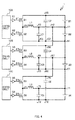
- Fig. 4 illustrates an example of a balance correction circuit 1 adapted to equalize the voltages of the four power storage cells B1 to B4.
- this balance correction circuit 1 includes a circuit (hereinafter this circuit is also called the first balance correction unit) configured to include the control circuit 10A, the gate drivers G1, G2, the switching elements S1, S2, the inductor L1 and the capacitive elements C1, C2 to control the charge/discharge of the power storage cells B1, B2, a circuit (hereinafter this circuit is also called the second balance correction unit) configured to include the control circuit 10B, the gate drivers G3, G4, the switching elements S3, S4, the inductor L2 and the capacitive elements C3, C4 to control the charge/discharge of the power storage cells B2, B3, and a circuit (hereinafter this circuit is also called the third balance correction unit) configured to include the control circuit 10C, the gate drivers G5, G6, the switching elements S5, S6, the inductor L3 and the capacitive elements C5, C6
- control circuit 10A complementarily turns on/off the switching elements S1, S2 to equalize the voltages of the power storage cells B1 and B2
- control circuit 10B complementarily turns on/off the switching elements S3, S4 to equalize the voltages of the power storage cells B2 and B3
- control circuit 10C complementarily turns on/off the switching elements S5, S6 to equalize the voltages of the power storage cells B3 and B4.
- Such control allows the voltage of the power storage cell B2 to be equal to the voltages of both of the two power storage cells B1, B3 and allows the voltage of the power storage cell B3 to be equal to the voltages of both of the two power storage cells B2, B4, and as a result the voltages of the four power storage cells B1, B2, B3 and B4 are equalized.
- the capacitive elements C1 to C6 are all provided for the purpose of reducing the noise generated due to the on/off operations of the switching elements S1 to S6 and relaxing the voltage variation generated to each of the power storage cells B1 to B4.
- each control circuit 10 (10A to 10C) can be operated independently, and also an on/off control of the switching element with one control circuit 10 can be performed in parallel with the on/off control of the switching element with another control circuit 10 (hereinafter this control will be called parallel control.)
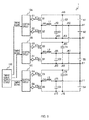
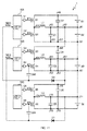
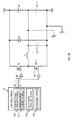
- Fig. 5 illustrates a balance correction circuit 1 shown as the first embodiment.
- This balance correction circuit 1 is configured with, as the basis, a balance correction circuit 1 adapted to equalize the voltages of the four power storage cells B1 to B4 shown in Fig. 4 .
- the common timing signals (e. g. , square-wave clock signal generated by an oscillator circuit and the like) generated in the timing signal supply device 100 (timing signal supply unit) is directly supplied to the control circuits 10A to 10C and the control circuits 10A to 10C generate the control signals ⁇ 1 to ⁇ 6 for on/off control of the switching elements S1 to S6 which are respectively the control targets based on the common timing signal supplied from the timing signal supply device 100.
- the timing signal supply device 100 is configured with, for example, a microcomputer, an oscillator circuit, a clock generator and the like, however, the timing signal supply device 100 may be configured as a part of any one of the control circuits 10.
- the balance correction circuit 1 in this way has each of the control circuits 10A to 10C generate the control signals ⁇ 1 to ⁇ 6 based on a common timing signal directly supplied from the same timing signal supply device 100 so that the control signals generated by the control circuits 10A to 10C are precisely synchronized and thus the above mentioned issues are prevented from occurring.
- Figs. 6 and 7 illustrate modified examples of the balance correction circuit 1 shown in Fig. 5 .
- the timing signal supply device 100 has supplied to the control circuits 10A to 10C the timing signals output from the same port by distributing with a common branch line commonly connected thereto.
- the balance correction circuit 1 has a timing signal directly supplied only to one control circuit 10 (control circuit 10C in Fig. 7 ) from the timing signal supply device 100, the timing signal supplied to this control circuit 10 from the control circuit 10 (control circuit 10C) is supplied to another control circuit (control circuit 10B in Fig.
- control circuit 10B the timing signal supplied to this control circuit 10 from the control circuit (control circuit 10B) is supplied to yet another control circuit (control circuit 10A).
- control circuit 10A the timing signal output from the timing signal supply device 100 is supplied to the control circuits 10A to 10C in a so-called bucket brigade manner.
- the number of output ports required for the timing signal of the timing signal supply device 100 need to be only one so that the resources of the timing signal supply device 100 can be utilized effectively.
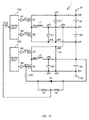
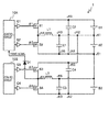
- Fig. 8 illustrates a balance correction circuit 1 shown as the second embodiment.
- This balance correction circuit 1 is configured with the balance correction circuit 1 adapted to equalize the voltages of three power storage cells B1 to B3 shown in Fig. 3 , as the basis.
- a timing signal is generated based on the control signal ⁇ 4 generated by the control circuit 10B of the second balance correction unit to be supplied to the control circuit 10A of the first balance correction unit.
- the second balance correction unit generates the timing signals in the following manner.
- this balance correction circuit 1 has a capacitive element C81 provided between the supply line to the switching element S4 of the control signal ⁇ 4 of the second balance correction unit and the cathode (connection point J67) of the power storage cell B3. Further, a rectifying element D1 (diode etc.) which allows a current to pass only in the direction from the power storage cell B3 cathode to the power storage cell B3 cathode side terminal of the capacitive element C81 is provided between the power storage cell B3 cathode and the power storage cell B3 cathode side terminal (connection point J69 side terminal) of the capacitive element C81.
- a rectifying element D1 diode etc.
- the power storage cell B3 cathode side terminal of the capacitive element C81 and the timing signal input terminal of the control circuit 10A are line connected so that the voltage at the power storage cell B3 cathode side terminal of the capacitive element C81 is supplied to the control circuit 10A as a timing signal.
- the capacitive element C81 is charged when the control signal ⁇ 4 is at a low level and the voltage of the power storage cell B3 cathode side terminal of the capacitive element C81 takes a value obtained by adding the power storage cell B3 cathode potential with the control signal ⁇ 4 voltage when the control signal ⁇ 4 is at a high level.
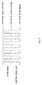
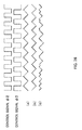
- Fig. 9 exemplifies a waveform of the control signal ⁇ 4 and a waveform of a timing signal provided to the control circuit 10A.
- the timing signal supplied to the control circuit 10A is in a waveform synchronizing with the control signal ⁇ 4.
- the timing signal is at a low level (potential of power storage cell B3 cathode) when the control signal ⁇ 4 is at a low level and the timing signal is at a high level (potential obtained by adding to the potential of the power storage cell B3 cathode with the voltage between the terminals of the capacitive element C81 charged by the control signal ⁇ 4) when the control signal ⁇ 4 is at a high level.
- the specific mechanism of the control circuit 10A generating the control signals ⁇ 1, ⁇ 2 based on the timing signal will be described later.
- the control circuit 10A of the first balance correction unit generates the control signals ⁇ 1, ⁇ 2 by synchronizing with the timing signals supplied from the second balance correction unit as described above. And when there is a need to adjust the voltage level of the timing signal, for example, as shown in Fig. 10 , only the voltage obtained by dividing the voltage between the terminals of the rectifying element D1 with the resistive elements R1, R2 has to be supplied to the control circuit 10A as a timing signal.
- FIG. 11 illustrates an example of a case where the mechanism is applied to a balance correction circuit 1 adapted to equalize the voltages of the four power storage cells B1 to B4.
- This balance correction circuit 1 is configured using the balance correction circuit 1 shown in Fig. 1 as the basis.
- a timing signal is generated based on the control signal ⁇ 6 generated by the control circuit 10C of the third balance correction unit to be supplied to the control circuit 10B of the second balance correction unit. Further, a timing signal is generated based on the control signal ⁇ 4 generated by the control circuit 10B of the second balance correction unit based on the above described timing signal for supply to the control circuit 10A of the first balance correction unit.
- Fig. 12 illustrates an example of a waveform of a control signal ⁇ 6 and a waveform of a timing signal supplied to the control circuit 10B.
- the timing signal supplied to the control circuit 10B is in a waveform synchronizing with the control signal ⁇ 6.
- the timing signal is at a low level (potential of power storage cell B4 cathode) when the control signal ⁇ 6 is at a low level and the timing signal is at a high level (potential obtained by adding to the potential of power storage cell B4 cathode the voltage between terminals of the capacitive element C81 charged by the control signal ⁇ 6) when the control signal ⁇ 6 is at a high level.
- Fig. 13 exemplifies a waveform of a control signal ⁇ 4 and a waveform of a timing signal supplied to the control circuit 10A.
- the timing signal supplied to the control circuit 10A is in a waveform synchronizing with the control signal ⁇ 4.
- the timing signal is at a low level (potential of power storage cell B3 cathode) when the control signal ⁇ 4 is at a low level and the timing signal is at a high level (potential obtained by adding to the potential of the power storage cell B3 cathode the voltage between the terminals of the capacitive element C82 charged by the control signal ⁇ 4) when the control signal ⁇ 4 is at a high level.
- the specific mechanism of the control circuit 10A generating the control signals ⁇ 1, ⁇ 2 based on the timing signal will be described later.
- the control circuit 10B of the second balance correction unit generates the control signals ⁇ 3, ⁇ 4 while allowing synchronization with the timing signals supplied from the third balance correction unit as described above.
- the control circuit 10A of the first balance correction unit generates the control signals ⁇ 1, ⁇ 2 while allowing synchronization with the timing signals supplied from the second balance correction unit as described above.
- the control circuit 10B or control circuit 10A as a timing signal.
- control signals can be precisely synchronized between or among the control circuits 10 according to the balance correction circuit 1 of the second embodiment since a timing signal generated based on a control signal generated by the control circuit 10 of one balance correction unit is supplied to the control circuit 10 of another balance correction unit for the another balance correction unit to generate a control signal based on this timing signal. Therefore, the aforementioned issues arising from the control signals not being synchronized can be prevented.
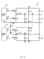
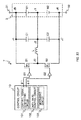
- Fig. 14 illustrates a balance correction circuit 1 shown as the third embodiment.
- This balance correction circuit 1 is configured with a balance correction circuit 1 adapted to equalize the voltages of the three power storage cells B1 to B3 shown in Fig. 3 , as the basis.
- timing signals are generated based on the control signals ⁇ 3, ⁇ 4 generated by the control circuit 10B of the second balance correction unit to be supplied to the control circuit 10A of the first balance correction unit.
- the voltage at the common connection point J64 (line including the common connection point) among the switching element S1, the switching element S2 and the inductor L2 of the control circuit 10B in the second balance correction unit is supplied to the control circuit 10A via the rectifying element D1 (diode etc.)
- Fig. 15 exemplifies a waveform at a common connection point J64 and a waveform of a timing signal supplied to the control circuit 10A.
- the timing signal supplied to the control circuit 10A is in a waveform synchronizing with the waveform synchronizing with the common connection point J64, that is, a waveform synchronizing with the control signals ⁇ 3, ⁇ 6. Further, as shown in Fig.
- the timing signal is at a low level (potential of power storage cell B3 cathode) when the waveform at the common connection point J64 is at a low level and the timing signal is at a high level (potential of power storage cell B2 cathode) when the waveform at the common connection point J64 is at a high level.
- the control circuit 10A of the first balance correction unit generates the control signals ⁇ 1, ⁇ 2 by allowing synchronization with the timing signals supplied from the second balance correction unit as described above. And when there is a need to adjust the voltage level of the timing signal depending on the configuration of the control circuit 10A side, for example as shown in Fig. 16 , the voltage level just has to be adjusted by inserting in series a resistive element R1 between the common connection point J64 and the timing signal input terminal of the control circuit 10A as well as inserting a resistive element R2 between the power storage cell B3 cathode and the timing signal input terminal of the control circuit 10A.
- FIG. 17 illustrates an example of a case where the mechanism is applied to a balance correction circuit 1 adapted to equalize the voltages of the four power storage cells B1 to B4.
- This balance correction circuit 1 is configured with the balance correction circuit 1 shown in Fig. 4 as the basis.
- a timing signal is generated based on the control signals ⁇ 5, ⁇ 6 generated by the control circuit 10C of the third balance correction unit to be supplied to the control circuit 10B of the second balance correction unit. Further, a timing signal is generated based on the control signals ⁇ 3, ⁇ 4 generated by the control circuit 10B of the second balance correction unit based on the above described timing signal supplied from the third balance correction unit to supply to the control circuit 10A of the first balance correction unit.
- Fig. 18 illustrates an example of a waveform at the common connection point J74 and a waveform of a timing signal supplied to the control circuit 10B.
- the timing signal supplied to the control circuit 10B is in a waveform synchronizing with the waveform at the common connection point J74, that is, in a waveform synchronizing with the control signals ⁇ 5, ⁇ 6. Further, as shown in Fig.
- the timing signal is at a low level (potential of power storage cell B4 cathode) when the waveform at the common connection point J74 is at a low level and the timing signal is at a high level (potential of power storage cell B4 cathode) when the waveform at the common connection point J74 is at a high level.
- Fig. 19 illustrates an example of a waveform at the common connection point J64 and a waveform of a timing signal supplied to the control circuit 10A.
- the timing signal supplied to the control circuit 10A is in a waveform synchronizing with the waveform at the common connection point J64, that is, in a waveform synchronizing with the control signals ⁇ 3, ⁇ 4.
- the timing signal is at a low level (potential of power storage cell B3 cathode) when the waveform at the common connection point J64 is at a low level and the timing signal is at a high level (potential of power storage cell B2 cathode) when the waveform at the common connection point J64 is at a high level.
- control signals can be precisely synchronized between or among the control circuits 10 according to the balance correction circuit 1 of the third embodiment since a timing signal generated based on a control signal generated by the control circuit 10 of one balance correction unit is supplied to the control circuit 10 of another balance correction unit for the another balance correction unit to generate a control signal based on this timing signal. Therefore, the aforementioned issues arising from the control signals not being synchronized can be prevented.
- the balance correction circuit 1 of the third embodiment need not have provided a capacitive element as in the second embodiment since the timing signal generated based on the voltage at the connection point common to the two switching elements S1 and the inductor L in the control circuit 10 of one balance correction unit is supplied to the control circuit 10 of another balance correction unit. Therefore, a mechanism for precisely synchronizing the control signals of the control circuits 10 can be realized in a further simplified configuration.
- control circuit 10 generates control signals based on the supplied timing signals in, for example, the following manner.
- Fig. 20 illustrates a configuration of the balance correction circuit 1 described in the first to the third embodiments (the balance correction unit 1 is drawn in a generalized manner in Fig. 20 .)
- the control circuit 10 includes a control signal generating circuit 101, a duty ratio control circuit 102 and a measuring circuit 103.
- the basic configurations of these circuits are as aforementioned.
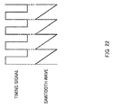
- the control signal generating circuit 101 includes a sawtooth wave generating circuit 1011.
- the sawtooth wave generating circuit 1011 generates a sawtooth wave synchronizing with the input timing signal.
- Fig. 21 only shows control signals ⁇ i.
- the sawtooth wave generating circuit 1011 for example, as illustrated in Fig. 22 , generates a sawtooth wave synchronizing with a timing signal by resetting to the maximum value (or minimum value) the sawtooth wave at a timing when the timing signal transitions from a low level to a high level (inverse theory (high level to low level) may do.)
- control circuit 10 can generate control signals (control signals ⁇ i, ⁇ i+1) which are synchronized with the timing signals input from the outside.
- the balance correction circuit according to the present invention may be provided separate from the power storage cell or may configure a battery pack and the like which is made integral with a power storage cell.
Abstract
Description
- The present invention relates to a balance correction device and a power storage device that equalize the voltages of power storage cells or power storage modules including a plurality of series connected power storage cells, in an assembled battery including a plurality of series connected power storage cells.
- In an assembled battery configured of a plurality of series connected power storage cells, there is a need to suppress the variances of the voltages (electromotive force) of the power storage cells in order to prevent a discharge capacity reduction and life shortening. Particularly, as in a power storage device used for electric vehicles and the like, there is a need to precisely suppress the voltage variances of the power storage cells in an assembled battery configured of multiple power storage cells.
- As a mechanism for equalizing the voltages of the power storage cells, for example,
PTL 1 discloses a so-called converter type balance correction method where one end of the inductor L is connected beforehand to a connection point of the series connected secondary batteries B1, B2 and the voltages of the batteries B1 and B2 are equalized by performing for an appropriate period, a repeated short time alternating operation (switching operation) between the first mode where an electric current flows through the first closed circuit formed by connecting the other end of the inductor L to the other end of the battery B1 and the second mode where an electric current flows through the second closed circuit formed by connecting the other end of the inductor L to the other end of the battery B2. - [PTL 1] Japanese Patent Application Laid-open Publication No.
2001-185229 -
Fig. 23 illustrates an example of a converter typebalance correction circuit 7. As shown inFig. 23 , the power storage cells B1 and B2 are connected in series to configure the assembledbattery 3. The power storage cell B1 has connected between the positive and negative terminals thereof a switching element S1 as well as a capacitive element C1, and the power storage cell B2 has connected between the positive and negative terminals thereof a switching element S2 as well as a capacitive element C2, respectively. Further, an inductor L is connected between the common connection point J3 of the switching elements S1 and S2, and the connection point J1 of the power storage cells B1 and B2. - The switching elements S1, S2 operate complementarily such that when one switching element is turned on, the other switching element is turned off with the gate drivers G1, G2 which are controlled by the control signals ϕ1, ϕ2 that are generated by the
control circuit 10. The capacitive elements C1, C2 are provided for the purpose of, for example, reducing the noise created due to the on/off operations of the switching elements, relieving the voltage difference created between the power storage cells B1, B2 due to the on/off operations of the switching elements. - The
control circuit 10 controls the on/off of the switching elements S1 and S2 alternatively at a predetermined duty ratio by controlling the gate drivers G1, G2 with the control signals ϕ1, ϕ2. Hereby, energy is exchanged between the power storage cells B1 and B2 via the inductor L to equalize the voltages of the power storage cells B1 and B2, as a result. - In
Fig. 24 , (a) illustrates the waveforms of the control signals ϕ1, ϕ2 which are generated by thecontrol circuit 10 during the on/off control period of the switching elements S1, S2. During the above period, thecontrol circuit 10 generates, for example, the control signals ϕ1, ϕ2 which are configured of square-waves with the on/off operations being performed complementarily in the same cycle, as illustrated in (a) ofFig. 24 . - In
Fig. 24 , (b) to (d) show the waveforms of the currents iL (hereinafter also called regenerated current) flowing through the inductor L during the on/off control period of the switching elements S1, S2. Among the figures inFig. 24 , (b) shows the waveform of the current iL flowing through the inductor L when the voltage E1 of the power storage cell B1 is higher than the voltage E2 of the power storage cell B2, (c) shows the waveform of the current iL flowing through the inductor L when the voltage E1 of the power storage cell B1 is lower than the voltage E2 of the power storage cell B2, and (d) shows the waveform of the current iL flowing through the inductor L when the voltage E1 of the power storage cell B1 is equal (substantially equal) to the voltage E2 of the power storage cell B2. - When there is a voltage difference between the two power storage cells B1, B2, energy is exchanged between the power storage cells B1 and B2 by the current iL alternatively flowing along the first path and the second path. And as a result, the voltages between the two are equalized to thereby secure a balance.
- The configuration indicated above are of a case where the number of the power storage cells is two, however, the configuration can be extended for a case where there are three or more power storage cells.
-
Fig. 25 illustrates an example of thebalance correction circuit 7 which is adapted to equalize the voltages of three power storage cells B1 to B3. InFig. 25 , thecontrol circuit 10A equalizes the voltages of the power storage cells B1 and B2 by complementarily turning on/off the switching elements S1, S2, and thecontrol circuit 10B equalizes the voltages of the power storage cells B2 and B3 by complementarily turning on/off the switching elements S3, S4. The voltage of the power storage cell B2 is equalized with both of the power storage cells B1, B3 with such control, and as a result thereof, the voltages of the three power storage cells B1, B2 and B3 are equalized. - In the
balance correction circuit 7 shown inFig. 25 , thecontrol circuits control circuit 10A can control the on/off of the switching elements S1, S2 in parallel with thecontrol circuit 10B controlling the on/off of the switching elements S3, S4 (hereinafter also called, parallel control.) When parallel control is performed, however, for example, if the frequencies of the control signals input (provided to the gate of the switching element) to the switching element during on/off control of the switching elements by each of thecontrol circuits -
Fig. 26 exemplifies the control signal ϕ2 waveform of the switching element S2, the control signal ϕ3 waveform of the switching element S3, and the voltage waveforms of the connection point inFig. 25 (the waveforms obtained by the on/off control of the switching elements S1, S2 with thecontrol circuit 10A (waveform having attached the reference character (a), the waveform obtained by the on/off control of the switching elements S3, S4 with thecontrol circuit 10B (waveform having attached the reference character (b), and the waveform obtained by superimposing (combining) the waveform attached reference character (a) with the waveform attached the reference character (b) (waveform having attached the reference character (c)) when the above described parallel control is performed. Although the waveforms ϕ1, ϕ4 of the switching elements S1, S4 are not illustrated inFig. 26 , the waveform of the control signal ϕ1 has a phase opposite that of the waveform of the control signal ϕ2 and the waveform of the control signal ϕ4 has a phase opposite that of the waveform of the control signal ϕ3. - As shown in
Fig. 26 , the phase difference between the control signals ϕ2 and ϕ3 changes along with time since the two are not synchronized. Along with this, the phase difference between the waveform indicated with the reference character (a) and the waveform indicated with the reference character (b) also changes. Therefore, the actual voltage waveform (c) that appears at the connection point J42 is a disordered waveform which includes multiple frequency components and is unstable with respect to time. Such a voltage waveform may be the cause for developing issues such as disturbance and noise, an abnormal regenerated current, abnormal oscillation and the like. - The present invention has been made in view of the above described problems and a subject thereof is to provide a balance correction device and a power storage device which can prevent problems caused by the signals controlling the switching elements being unsynchronized in the control circuits.
- An invention of the present inventions for achieving the above described objective is a balance correction device that is in an assembled battery including a plurality of series connected power storage cells and equalizes voltages of the power storage cells or of power storage modules that include the series connected power storage cells, the balance correction device comprising: a plurality of balance correction units including an inductor that has one end thereof connected to a connection point between a first one of the power storage modules and a second one of the power storage modules connected in series, a first switching element that is series connected together with the inductor between positive and negative terminals of the first power storage module, a second switching element that is series connected together with the inductor between positive and negative terminals of the second power storage module, a switching control unit that controls a supply of a current to each of the power storage modules by an on/off control of the first switching element and the second switching element to equalize the voltages of the power storage modules by exchanging electric power of the power storage modules via the inductor; and a timing signal supply unit that has the first power storage module of one of the balance correction units line connected with the second power storage module of another one of the balance correction units to be a same one of the power storage modules, and supplies to the respective switching control unit of the balance correction units, a common timing signal used to generate a control signal to input to the first switching element and the second switching element to on/off control the first switching element and the second switching element.
- Another of the present inventions is the aforementioned balance correction device wherein the timing signal supply unit directly supplies the timing signal to the respective switching control unit of the balance correction units.
- Another of the present inventions is the aforementioned balance correction device wherein the timing signal supply unit includes a first circuit that supplies the timing signal to the switching control unit of a second one of the balance correction units and a second circuit that supplies the timing signal supplied from the timing signal supply unit by the second balance correction unit, to the switching control unit of a first one of the balance correction units.
- Another of the present inventions is the aforementioned balance correction device wherein the second circuit generates a timing signal based on the control signal that the switching control unit of the second balance correction unit generates and supplies the generated timing signal to the switching control unit of the first balance correction unit.
- Another of the present inventions is the aforementioned balance correction device wherein the second circuit generates the timing signal based on a variation in voltages applied to a capacitive element that is charged by a voltage difference created between the control signal that is generated by the switching control unit of the second balance correction unit and a cathode of the second power storage module of the second balance correction unit.
- Another of the present inventions is the aforementioned balance correction device wherein the second circuit charges the capacitive element by a voltage obtained by rectifying a voltage applied to the capacitive element.
- Another of the present inventions is the aforementioned balance correction device wherein the second circuit generates the timing signal based on a divided voltage obtained by dividing a voltage applied to the capacitive element.
- Another of the present inventions is the aforementioned balance correction device wherein the second circuit generates the timing signal based on a voltage generated at a common connection part of the first switching element and the second switching element of the switching control unit of the second balance correction unit and the inductor.
- Another of the present inventions the aforementioned balance correction device wherein the second circuit generates the timing signal based on a variation in voltages obtained by rectifying the voltages generated at the common connection part.
- Another of the present inventions is the aforementioned balance correction device wherein the second circuit generates the timing signal based on a variation in voltages obtained by dividing the voltages generated at the common connection part.
- Another of the present inventions is a power storage device including the plurality of power storage cells and the balance correction device.
- Other problems disclosed by the present application and the methods for solving such problems will become clear from the description of embodiments with reference to the accompanying drawings.
- According to the present invention, issues arising from the signals controlling the switching elements being unsynchronized in the control circuits can be prevented.
-
- [
Fig. 1 ]
Fig .1 illustrates an example of abalance correction circuit 1. - [
Fig. 2 ]
Fig. 2 illustrates in (a) a waveform of the control signals ϕ1, ϕ2 output by thecontrol circuit 10 during the first period and (b) to (d) waveforms of currents flowing through the inductor L during the first period. - [
Fig. 3 ]
Fig. 3 illustrates an example of a balance correction circuit adapted to equalize the voltages of three power storage cells B1 to B3. - [
Fig. 4 ]
Fig. 4 illustrates an example of a balance correction circuit adapted to equalize the voltages of four power storage cells B1 to B4. - [
Fig. 5 ]
Fig. 5 illustrates abalance correction circuit 1 shown as the first embodiment. - [
Fig. 6 ]
Fig. 6 illustrates a modified example of thebalance correction circuit 1 shown as the first embodiment. - [
Fig. 7 ]
Fig. 7 illustrates a modified example of thebalance correction circuit 1 shown as the first embodiment. - [
Fig. 8 ]
Fig. 8 illustrates a balance correction circuit 1 (in a case of three power storage cells) shown as the second embodiment. - [
Fig. 9 ]
Fig. 9 illustrates an example of a voltage waveform of a control signal ϕ4 and a voltage waveform of a timing signal provided to thecontrol circuit 10A. - [
Fig. 10 ]
Fig. 10 illustrates a modified example of thebalance correction circuit 1 shown as the second embodiment. - [
Fig. 11 ]
Fig. 11 illustrates a balance correction circuit 1 (in a case of four power storage cells) shown as the second embodiment. - [
Fig. 12 ]
Fig. 12 illustrates an example of a voltage waveform of a control signal ϕ6 and a voltage waveform of a timing signal provided to thecontrol circuit 10B. - [
Fig. 13 ]
Fig. 13 illustrates an example of a voltage waveform of the control signal ϕ4 and a voltage waveform of the timing signal provided to thecontrol circuit 10A. - [
Fig. 14 ]
Fig. 14 illustrates a balance correction circuit 1 (in a case of three power storage cells) shown as the third embodiment. - [
Fig. 15 ]
Fig. 15 illustrates an example of a voltage waveform at a common connection point J64 of the second balance correction unit and a voltage waveform of a timing signal provided to thecontrol circuit 10A. - [
Fig. 16 ]
Fig. 16 illustrates a modified example of thebalance correction circuit 1 shown as the third embodiment. - [
Fig. 17 ]
Fig. 17 illustrates a balance correction circuit 1 (in a case of four power storage cells) shown as the third embodiment. - [
Fig. 18 ]
Fig. 18 illustrates an example of a voltage waveform of a control signal ϕ6 and a voltage waveform of a timing signal provided to thecontrol circuit 10B. - [
Fig. 19 ]
Fig. 19 illustrates an example of a voltage waveform of a control signal ϕ4 and a voltage waveform of a timing signal provided to thecontrol circuit 10A. - [
Fig. 20 ]
Fig. 20 is a diagram illustrating a mechanism of thecontrol circuit 10 generating control signals which synchronize with the timing signal. - [
Fig. 21 ]
Fig. 21 is a diagram illustrating how the controlsignal generating circuit 101 generates control signals ϕi,ϕi+ 1. - [
Fig. 22 ]
Fig. 22 is a diagram illustrating a mechanism of the sawtoothwave generating circuit 1011 generating a sawtooth wave synchronizing with the timing signal. - [
Fig. 23 ]
Fig. 23 illustrates an example of a converter typebalance correction circuit 7. - [
Fig. 24 ]
Fig. 24 illustrates in (a) waveforms of the control signals ϕ1, ϕ2 output by thecontrol circuit 10 during the first period and (b) to (d) waveforms of currents flowing through the inductor L during the first period. - [
Fig. 25 ]
Fig. 25 illustrates an example of abalance correction circuit 7 adapted to equalize the voltages of three power storage cells B1 to B3. - [
Fig. 26 ]
Fig. 26 illustrates an example of a waveform generated at the connection point J42 when the frequencies of the control signals are not synchronized. - The present application claims the benefit of priority to Japanese Patent Application No.
2013-238225, filed on November 18, 2013 - Description of the embodiments according to the present invention will be given in the following. In the following description, the same or similar parts are attached the same reference numbers to omit duplicate description. Index letters may be omitted from the reference numbers to collectively call the same constituent element (e.g.,
control circuits control circuit 10.) <Basic Configuration of Balance Correction Circuit> -
Fig .1 illustrates an example of a converter type balance correction circuit 1 (balance correction device.) Thebalance correction circuit 1 is, for example, applied to power storage devices (electric vehicles, hybrid vehicles, electric two-wheeled vehicles, railway vehicles, elevators, system tied power storage devices, personal computers, laptop computers, mobile telephone devices, smartphones, PDA instruments etc.) which use an assembled battery including a plurality of series connected power storage cells. A power storage cell is, for example, a lithium ion secondary battery, a lithium ion polymer secondary battery and the like, however, may be other types of power storage elements such as an electric double layer capacitor. - If the degree of manufacturing quality or deterioration differ in the power storage cells configuring the assembled battery, difference in the battery characteristics (battery capacity, discharge voltage characteristics) in the power storage cells may be created so that the voltages of the power storage cells may vary during the charging/discharging of electricity due to the difference in the battery characteristics. For such reason, the
balance correction circuit 1 operates to equalize (ensure cell balance) the voltages of power storage cells or of power storage modules configured of a plurality of series connected power storage cells in order to suppress generation of variances as above. - As illustrated in
Fig. 1 , the assembledbattery 3 is configured with series connected power storage cells B1, B2. The positive andnegative terminals battery 3 have connected thereto, for example, a current supply source (e.g., recharger, regeneration circuit) which supplies a charging current to the assembledbattery 3, a load (e.g., motor, electronic circuit, electrical appliances) which function by using the electromotive force of the assembledbattery 3 and the like. - The line (line including the point connecting the power storage cells B1, B2 in series) connecting the anode of the power storage cell B1 and the cathode of the power storage cell B2 has connected thereto one end of the inductor L. The line connecting the other end of the inductor L and the cathode of the power storage cell B1 has provided a switching element S1. And the line connecting the other end of the inductor L and the anode of the power storage cell B2 has provided a switching element S2.
- The switching elements S1, S2 is configured using a MOSFET (Metal-Oxide-Semiconductor Field-Effect Transistor). The switching elements S1, S2 operate complementarily with the gate drivers G1, G2 which are controlled by the control signals ϕ1, ϕ2 that are generated by the control circuit 10 (switching control unit) such that when one switching element is turned on, the other switching element is turned off. Here, the switching elements S1, S2 may be configured using a bipolar transistor.
- A capacitive element C1 is provided between one end of the inductor L and the cathode of the power storage cell B1, and a capacitive element C2 is provided between one end of the inductor L and the anode of the power storage cell B2. The capacitive elements C1, C2 are provided for the purpose of, for example, reducing noise generated due to the on/off operations of the switching element, variation in the voltages generated between the power storage cells B1, B2 due to the on/off operations of the switching element and the like. The capacitive element C1 may be provided between, for example, the cathode of the power storage cell B1 and the anode of the power storage cell B2.
- The
control circuit 10 includes a controlsignal generating circuit 101, a dutyratio control circuit 102 and a measuring circuit 103 (voltage measuring unit.) Thecontrol circuit 10 can be implemented by using a microcomputer including, for example, an arithmetic device (CPU (Central Processing Unit), MPU (Micro Processing Unit) etc.) and a storage device (RAM (Random Access Memory), ROM (Read Only Memory) etc.). - The control
signal generating circuit 101 generates diphase control signals ϕ1, ϕ2 to be respectively supplied to the gate drivers G1, G2. Specifically, the controlsignal generating circuit 101 generates the control signals ϕ1, ϕ2 according to the later described duty ratio control signal which is input from the dutyratio control circuit 102. The control signals ϕ1, ϕ2 in the present embodiment are assumed to be diphase (high level, low level) square-waves (e.g., PWM (Pulse Width Modulation) pulses) of a predetermined duty ratio. - The duty
ratio control circuit 102 generates signals (hereinafter called duty ratio control signals) for controlling the control signals ϕ1, ϕ2 generated by the controlsignal generating circuit 101 and inputs the generated duty ratio control signals to the controlsignal generating circuit 101. The dutyratio control circuit 102 generates the duty ratio control signals so that the voltages between the power storage cells B1, B2 are appropriately equalized in view of improving the speed, safety, efficiency and the like according to, for example, the voltages of the power storage cells B1, B2 obtained from the measurements of the measuringcircuit 103. - The measuring
circuit 103 obtains the real time measurements of the voltages (e.g., voltage between the connection points J4 and J2, voltage between the connection points J2 and J7 etc.) at a predetermined part of the line which configures thebalance correction circuit 1 and transmits the measurements obtained to the controlsignal generating circuit 101 and the dutyratio control circuit 102. - Next, description on the basic operations of the
balance correction circuit 1 configured as described above will be given with reference toFig. 2 . - In
Fig. 2 , (a) shows the waveform of the control signals ϕ1, ϕ2 which are generated during the period when the on/off control of the switching elements S1, S2 are performed by thecontrol circuit 10. During the above period, thecontrol circuit 10 generates, for example, the control signals ϕ1, ϕ2 which are configured of square-waves formed by complementarily turning on/off at the same cycle. - In
Fig. 2 , (b) to (d) show the waveforms of the currents iL which flow through the inductor L (hereinafter also called the regeneration circuit) during the on/off control period of the switching elements S1, S2. Among them, (b) shows the waveform of the current iL which flows through the inductor L when the voltage E1 of the power storage cell B1 is higher than the voltage E2 of the power storage cell B2, (c) shows the waveform of the current iL which flows through the inductor L when the voltage E1 of the power storage cell B1 is lower than the voltage E2 of the power storage cell B2, and (d) shows the waveform of the current iL which flows through the inductor L when the voltage E1 of the power storage cell B1 and the voltage E2 of the power storage cell B2 are equal (substantially equal.) - As shown in (b) of
Fig. 2 , when the voltage E1 of the power storage cell B1 is higher than the voltage E2 of the power storage cell B2 (E1>E2), a current iL mainly flows along a path (hereinafter called the first path) from the cathode of the power storage cell B1 -> the connection point J5 -> the connection point J4 -> the switching element S1 -> the connection point J3 -> the inductor L -> the connection point J2 -> the connection point J1 -> and to the anode of the power storage cell B1 while the switching element S1 is turned on and the switching element S2 is turned off. That is, during this period, the current iL mainly flows in the direction shown with the solid arrow indicated inFig. 1 to have energy stored in the inductor L. - Thereafter, when the switching element S1 is turned off and the switching element S2 is turned on, the energy stored in the inductor L is discharged along the path from the inductor L -> the connection point J2 -> the connection point J1 -> the cathode of the power storage cell B2 -> the anode of the power storage cell B2 -> the connection point J6 -> the connection point J7 -> the switching element S2 -> the connection point J3 -> and to the inductor L to hereby charge the power storage cell B2. And when the energy in the inductor L is exhausted, the current iL starts flowing toward the opposite direction (the direction shown with a dashed arrow in
Fig. 1 ) in the inductor L. - As shown in (c) of
Fig. 2 , when the voltage E1 of the power storage cell B1 is lower than the voltage E2 of the power storage cell B2 (E1<E2), a current iL mainly flows along a path (hereinafter called the second path) from the cathode of the power storage cell B2 -> the connection point J1 -> the connection point J2 -> the inductor L -> the connection point J3 -> the switching element S2 -> the connection point J7 -> the connection point J6 -> and to the anode of the power storage cell B2 while the switching element S1 is turned off and the switching element S2 is turned on. That is, during this period, the current iL mainly flows in the direction shown with the dashed arrow indicated inFig. 1 to have energy stored in the inductor L. - Thereafter, when the switching element S2 is turned off and the switching element S1 is turned on, the energy stored in the inductor L is discharged along the path from the inductor L -> the connection point J3 -> the switching element S1 -> the connection point J4 -> the connection point J5 -> the cathode of the power storage cell B1 -> the anode of the power storage cell B1 -> the connection point J1 -> the connection point J2 -> and to the inductor L to hereby charge the power storage cell B1. And when the energy in the inductor L is exhausted, the current iL starts flowing toward the opposite direction (the direction shown with a solid arrow in
Fig. 1 ) in the inductor L. - Hereby, when there is a difference between the voltages of the power storage cells B1, B2, energy is exchanged between the power storage cell B1 and the power storage cell B2 by the current iL alternatively flowing through the first path and the second path to equalize the voltages of the two and ensuring a cell balance as a result. As shown in (d) of
Fig. 2 , when the voltage E1 of the power storage cell B1 and the voltage E2 of the power storage cell B2 are equal (E1=E2), the tradeoff of the energy exchanged between the power storage cells B1, B2 is balanced along with the on/off control of the switching elements S1, S2 so that the voltages of the power storage cells B1, B2 are maintained equal. - The
control circuit 10 performs realtime monitoring of the voltages (voltage between the respective terminals of the power storage cells B1, B2, for example, the voltage between the connection points J4 and J2, voltage between the connection points J2 and J7) measured with the measuringcircuit 103, and stops the on/off control of the switching elements S1, S2 upon detecting that the voltages of the power storage cells B1, B2 are equal (substantially equal.) - Here, the
control circuit 10 may control the duty ratio of the control signals ϕ1, ϕ2 according to, for example, the voltage values of the power storage cells B1, B2 obtained from the measurements of the measuringcircuit 103 so that the voltages between the power storage cells B1, B2 are appropriately equalized in view of improving the speed, safety, efficiency and the like. <In a Case of Three or More Power Storage Cells> - The configuration of the
balance correction circuit 1 described above can be extended for a case where there are three of more power storage cells. -
Fig. 3 illustrates an example of abalance correction circuit 1 adapted to equalize the voltages of three power storage cells B1 to B3. As shown inFig. 3 , thisbalance correction circuit 1 includes a circuit (hereinafter this circuit is also called the first balance correction unit) configured to include thecontrol circuit 10A, the gate drivers G1, G2, the switching elements S1, S2, the inductor L1 and the capacitive elements C1, C2 to control the charge/discharge of the power storage cells B1, B2, and a circuit (hereinafter this circuit is also called the second balance correction unit) configured to include thecontrol circuit 10B, the gate drivers G3, G4, the switching elements S3, S4, the inductor L2 and the capacitive elements C3, C4 to control the charge/discharge of the power storage cells B2, B3. - In
Fig. 3 , thecontrol circuit 10A complementarily turns on/off the switching elements S1, S2 to equalize the voltages of the power storage cells B1 and B2, and thecontrol circuit 10B complementarily turns on/off the switching elements S3, S4 to equalize the voltages of the power storage cells B2 and B3. Such control allows the voltage of the power storage cell B2 to be equal to the voltages of both of the two power storage cells B1, B3 and as a result the voltages of the three power storage cells B1, B2 and B3 are equalized. - In
Fig. 3 , the capacitive elements C1 to C4 are all provided for the purpose of reducing the noise generated due to the on/off operations of the switching elements S1 to S4 and relaxing the voltage variation generated to each of the power storage cells B1 to B3. -
Fig. 4 illustrates an example of abalance correction circuit 1 adapted to equalize the voltages of the four power storage cells B1 to B4. As shown inFig. 4 , thisbalance correction circuit 1 includes a circuit (hereinafter this circuit is also called the first balance correction unit) configured to include thecontrol circuit 10A, the gate drivers G1, G2, the switching elements S1, S2, the inductor L1 and the capacitive elements C1, C2 to control the charge/discharge of the power storage cells B1, B2, a circuit (hereinafter this circuit is also called the second balance correction unit) configured to include thecontrol circuit 10B, the gate drivers G3, G4, the switching elements S3, S4, the inductor L2 and the capacitive elements C3, C4 to control the charge/discharge of the power storage cells B2, B3, and a circuit (hereinafter this circuit is also called the third balance correction unit) configured to include thecontrol circuit 10C, the gate drivers G5, G6, the switching elements S5, S6, the inductor L3 and the capacitive elements C5, C6 to control the charge/discharge of the power storage cells B3, B4. - In
Fig. 4 , thecontrol circuit 10A complementarily turns on/off the switching elements S1, S2 to equalize the voltages of the power storage cells B1 and B2, thecontrol circuit 10B complementarily turns on/off the switching elements S3, S4 to equalize the voltages of the power storage cells B2 and B3, and thecontrol circuit 10C complementarily turns on/off the switching elements S5, S6 to equalize the voltages of the power storage cells B3 and B4. Such control allows the voltage of the power storage cell B2 to be equal to the voltages of both of the two power storage cells B1, B3 and allows the voltage of the power storage cell B3 to be equal to the voltages of both of the two power storage cells B2, B4, and as a result the voltages of the four power storage cells B1, B2, B3 and B4 are equalized. - In
Fig. 4 , the capacitive elements C1 to C6 are all provided for the purpose of reducing the noise generated due to the on/off operations of the switching elements S1 to S6 and relaxing the voltage variation generated to each of the power storage cells B1 to B4. - In the
balance correction circuit 1 shown inFig. 3 orFig. 4 , each control circuit 10 (10A to 10C) can be operated independently, and also an on/off control of the switching element with onecontrol circuit 10 can be performed in parallel with the on/off control of the switching element with another control circuit 10 (hereinafter this control will be called parallel control.) - However, when the frequencies of the control signals input (imparted to the gate of the switching element) to the switching element are not synchronized when the
control circuits Fig. 3 and to the connection points J42, J67 in the case ofFig. 4 so that issues of disturbance and noise, abnormality in the regenerated current, abnormality in oscillation being generated and the like would arise. Specific configurations for preventing such issues will be described in the following. -
Fig. 5 illustrates abalance correction circuit 1 shown as the first embodiment. Thisbalance correction circuit 1 is configured with, as the basis, abalance correction circuit 1 adapted to equalize the voltages of the four power storage cells B1 to B4 shown inFig. 4 . - In this
balance correction circuit 1, the common timing signals (e. g. , square-wave clock signal generated by an oscillator circuit and the like) generated in the timing signal supply device 100 (timing signal supply unit) is directly supplied to thecontrol circuits 10A to 10C and thecontrol circuits 10A to 10C generate the control signals ϕ1 to ϕ6 for on/off control of the switching elements S1 to S6 which are respectively the control targets based on the common timing signal supplied from the timingsignal supply device 100. The timingsignal supply device 100 is configured with, for example, a microcomputer, an oscillator circuit, a clock generator and the like, however, the timingsignal supply device 100 may be configured as a part of any one of thecontrol circuits 10. - The
balance correction circuit 1 in this way has each of thecontrol circuits 10A to 10C generate the control signals ϕ1 to ϕ6 based on a common timing signal directly supplied from the same timingsignal supply device 100 so that the control signals generated by thecontrol circuits 10A to 10C are precisely synchronized and thus the above mentioned issues are prevented from occurring. -
Figs. 6 and7 illustrate modified examples of thebalance correction circuit 1 shown inFig. 5 . In thebalance correction circuit 1 shown inFig. 6 , the timingsignal supply device 100 has supplied to thecontrol circuits 10A to 10C the timing signals output from the same port by distributing with a common branch line commonly connected thereto. Further, as shown inFig. 7 , thebalance correction circuit 1 has a timing signal directly supplied only to one control circuit 10 (control circuit 10C inFig. 7 ) from the timingsignal supply device 100, the timing signal supplied to thiscontrol circuit 10 from the control circuit 10 (control circuit 10C) is supplied to another control circuit (control circuit 10B inFig. 7 ), and the timing signal supplied to thiscontrol circuit 10 from the control circuit (control circuit 10B) is supplied to yet another control circuit (controlcircuit 10A). In other words, the timing signal output from the timingsignal supply device 100 is supplied to thecontrol circuits 10A to 10C in a so-called bucket brigade manner. When the circuit configuration ofFig. 6 orFig. 7 is adopted, the number of output ports required for the timing signal of the timingsignal supply device 100 need to be only one so that the resources of the timingsignal supply device 100 can be utilized effectively. -
Fig. 8 illustrates abalance correction circuit 1 shown as the second embodiment. Thisbalance correction circuit 1 is configured with thebalance correction circuit 1 adapted to equalize the voltages of three power storage cells B1 to B3 shown inFig. 3 , as the basis. - In this
balance correction circuit 1, a timing signal is generated based on the control signal ϕ4 generated by thecontrol circuit 10B of the second balance correction unit to be supplied to thecontrol circuit 10A of the first balance correction unit. Specifically, the second balance correction unit generates the timing signals in the following manner. - As shown in
Fig. 8 , thisbalance correction circuit 1 has a capacitive element C81 provided between the supply line to the switching element S4 of the control signal ϕ4 of the second balance correction unit and the cathode (connection point J67) of the power storage cell B3. Further, a rectifying element D1 (diode etc.) which allows a current to pass only in the direction from the power storage cell B3 cathode to the power storage cell B3 cathode side terminal of the capacitive element C81 is provided between the power storage cell B3 cathode and the power storage cell B3 cathode side terminal (connection point J69 side terminal) of the capacitive element C81. And the power storage cell B3 cathode side terminal of the capacitive element C81 and the timing signal input terminal of thecontrol circuit 10A are line connected so that the voltage at the power storage cell B3 cathode side terminal of the capacitive element C81 is supplied to thecontrol circuit 10A as a timing signal. - In the above configuration, the capacitive element C81 is charged when the control signal ϕ4 is at a low level and the voltage of the power storage cell B3 cathode side terminal of the capacitive element C81 takes a value obtained by adding the power storage cell B3 cathode potential with the control signal ϕ4 voltage when the control signal ϕ4 is at a high level.
-
Fig. 9 exemplifies a waveform of the control signal ϕ4 and a waveform of a timing signal provided to thecontrol circuit 10A. As shown inFig. 9 , the timing signal supplied to thecontrol circuit 10A is in a waveform synchronizing with the control signal ϕ4. Further, as shown inFig. 9 , the timing signal is at a low level (potential of power storage cell B3 cathode) when the control signal ϕ4 is at a low level and the timing signal is at a high level (potential obtained by adding to the potential of the power storage cell B3 cathode with the voltage between the terminals of the capacitive element C81 charged by the control signal ϕ4) when the control signal ϕ4 is at a high level. The specific mechanism of thecontrol circuit 10A generating the control signals ϕ1, ϕ2 based on the timing signal will be described later. - The
control circuit 10A of the first balance correction unit generates the control signals ϕ1, ϕ2 by synchronizing with the timing signals supplied from the second balance correction unit as described above. And when there is a need to adjust the voltage level of the timing signal, for example, as shown inFig. 10 , only the voltage obtained by dividing the voltage between the terminals of the rectifying element D1 with the resistive elements R1, R2 has to be supplied to thecontrol circuit 10A as a timing signal. - A similar mechanism can be extended to the
balance correction circuit 1 which is adapted for a case including four or more power storage cells.Fig. 11 illustrates an example of a case where the mechanism is applied to abalance correction circuit 1 adapted to equalize the voltages of the four power storage cells B1 to B4. Thisbalance correction circuit 1 is configured using thebalance correction circuit 1 shown inFig. 1 as the basis. - As shown in
Fig. 11 , in thisbalance correction circuit 1, a timing signal is generated based on the control signal ϕ6 generated by thecontrol circuit 10C of the third balance correction unit to be supplied to thecontrol circuit 10B of the second balance correction unit. Further, a timing signal is generated based on the control signal ϕ4 generated by thecontrol circuit 10B of the second balance correction unit based on the above described timing signal for supply to thecontrol circuit 10A of the first balance correction unit. -
Fig. 12 illustrates an example of a waveform of a control signal ϕ6 and a waveform of a timing signal supplied to thecontrol circuit 10B. As shown inFig. 12 , the timing signal supplied to thecontrol circuit 10B is in a waveform synchronizing with the control signal ϕ6. Further, as shown inFig. 12 , the timing signal is at a low level (potential of power storage cell B4 cathode) when the control signal ϕ6 is at a low level and the timing signal is at a high level (potential obtained by adding to the potential of power storage cell B4 cathode the voltage between terminals of the capacitive element C81 charged by the control signal ϕ6) when the control signal ϕ6 is at a high level. -
Fig. 13 exemplifies a waveform of a control signal ϕ4 and a waveform of a timing signal supplied to thecontrol circuit 10A. As shown inFig. 13 , the timing signal supplied to thecontrol circuit 10A is in a waveform synchronizing with the control signal ϕ4. Further, as shown inFig. 13 , the timing signal is at a low level (potential of power storage cell B3 cathode) when the control signal ϕ4 is at a low level and the timing signal is at a high level (potential obtained by adding to the potential of the power storage cell B3 cathode the voltage between the terminals of the capacitive element C82 charged by the control signal ϕ4) when the control signal ϕ4 is at a high level. The specific mechanism of thecontrol circuit 10A generating the control signals ϕ1, ϕ2 based on the timing signal will be described later. - The
control circuit 10B of the second balance correction unit generates the control signals ϕ3, ϕ4 while allowing synchronization with the timing signals supplied from the third balance correction unit as described above. And thecontrol circuit 10A of the first balance correction unit generates the control signals ϕ1, ϕ2 while allowing synchronization with the timing signals supplied from the second balance correction unit as described above.
And when there is a need to adjust the voltage level of the timing signal, similar to the case of thebalance correction circuit 1 which is adapted for a case including three power storage cells, only the voltage obtained by dividing the voltage between the terminals of the rectifying element D1 (or rectifying element D2) has to be supplied to thecontrol circuit 10B (or controlcircuit 10A) as a timing signal. - As described above, the control signals can be precisely synchronized between or among the
control circuits 10 according to thebalance correction circuit 1 of the second embodiment since a timing signal generated based on a control signal generated by thecontrol circuit 10 of one balance correction unit is supplied to thecontrol circuit 10 of another balance correction unit for the another balance correction unit to generate a control signal based on this timing signal. Therefore, the aforementioned issues arising from the control signals not being synchronized can be prevented. -
Fig. 14 illustrates abalance correction circuit 1 shown as the third embodiment. Thisbalance correction circuit 1 is configured with abalance correction circuit 1 adapted to equalize the voltages of the three power storage cells B1 to B3 shown inFig. 3 , as the basis. - In this
balance correction circuit 1, timing signals are generated based on the control signals ϕ3, ϕ4 generated by thecontrol circuit 10B of the second balance correction unit to be supplied to thecontrol circuit 10A of the first balance correction unit. Specifically, in thisbalance correction circuit 1, the voltage at the common connection point J64 (line including the common connection point) among the switching element S1, the switching element S2 and the inductor L2 of thecontrol circuit 10B in the second balance correction unit is supplied to thecontrol circuit 10A via the rectifying element D1 (diode etc.) -
Fig. 15 exemplifies a waveform at a common connection point J64 and a waveform of a timing signal supplied to thecontrol circuit 10A. As shown inFig. 15 , the timing signal supplied to thecontrol circuit 10A is in a waveform synchronizing with the waveform synchronizing with the common connection point J64, that is, a waveform synchronizing with the control signals ϕ3, ϕ6. Further, as shown inFig. 15 , the timing signal is at a low level (potential of power storage cell B3 cathode) when the waveform at the common connection point J64 is at a low level and the timing signal is at a high level (potential of power storage cell B2 cathode) when the waveform at the common connection point J64 is at a high level. - The
control circuit 10A of the first balance correction unit generates the control signals ϕ1, ϕ2 by allowing synchronization with the timing signals supplied from the second balance correction unit as described above. And when there is a need to adjust the voltage level of the timing signal depending on the configuration of thecontrol circuit 10A side, for example as shown inFig. 16 , the voltage level just has to be adjusted by inserting in series a resistive element R1 between the common connection point J64 and the timing signal input terminal of thecontrol circuit 10A as well as inserting a resistive element R2 between the power storage cell B3 cathode and the timing signal input terminal of thecontrol circuit 10A. - A similar mechanism can be extended to the
balance correction circuit 1 which is adapted for a case including four or more power storage cells.Fig. 17 illustrates an example of a case where the mechanism is applied to abalance correction circuit 1 adapted to equalize the voltages of the four power storage cells B1 to B4. Thisbalance correction circuit 1 is configured with thebalance correction circuit 1 shown inFig. 4 as the basis. - As shown in
Fig. 17 , in thisbalance correction circuit 1, a timing signal is generated based on the control signals ϕ5, ϕ6 generated by thecontrol circuit 10C of the third balance correction unit to be supplied to thecontrol circuit 10B of the second balance correction unit. Further, a timing signal is generated based on the control signals ϕ3, ϕ4 generated by thecontrol circuit 10B of the second balance correction unit based on the above described timing signal supplied from the third balance correction unit to supply to thecontrol circuit 10A of the first balance correction unit. -
Fig. 18 illustrates an example of a waveform at the common connection point J74 and a waveform of a timing signal supplied to thecontrol circuit 10B. As shown inFig. 18 , the timing signal supplied to thecontrol circuit 10B is in a waveform synchronizing with the waveform at the common connection point J74, that is, in a waveform synchronizing with the control signals ϕ5, ϕ6. Further, as shown inFig. 18 , the timing signal is at a low level (potential of power storage cell B4 cathode) when the waveform at the common connection point J74 is at a low level and the timing signal is at a high level (potential of power storage cell B4 cathode) when the waveform at the common connection point J74 is at a high level. -
Fig. 19 illustrates an example of a waveform at the common connection point J64 and a waveform of a timing signal supplied to thecontrol circuit 10A. As shown inFig. 19 , the timing signal supplied to thecontrol circuit 10A is in a waveform synchronizing with the waveform at the common connection point J64, that is, in a waveform synchronizing with the control signals ϕ3, ϕ4. Further, as shown inFig. 19 , the timing signal is at a low level (potential of power storage cell B3 cathode) when the waveform at the common connection point J64 is at a low level and the timing signal is at a high level (potential of power storage cell B2 cathode) when the waveform at the common connection point J64 is at a high level. - As described above, the control signals can be precisely synchronized between or among the
control circuits 10 according to thebalance correction circuit 1 of the third embodiment since a timing signal generated based on a control signal generated by thecontrol circuit 10 of one balance correction unit is supplied to thecontrol circuit 10 of another balance correction unit for the another balance correction unit to generate a control signal based on this timing signal. Therefore, the aforementioned issues arising from the control signals not being synchronized can be prevented. - Further, the
balance correction circuit 1 of the third embodiment need not have provided a capacitive element as in the second embodiment since the timing signal generated based on the voltage at the connection point common to the two switching elements S1 and the inductor L in thecontrol circuit 10 of one balance correction unit is supplied to thecontrol circuit 10 of another balance correction unit. Therefore, a mechanism for precisely synchronizing the control signals of thecontrol circuits 10 can be realized in a further simplified configuration. - In the above described embodiments, the
control circuit 10 generates control signals based on the supplied timing signals in, for example, the following manner. -
Fig. 20 illustrates a configuration of thebalance correction circuit 1 described in the first to the third embodiments (thebalance correction unit 1 is drawn in a generalized manner inFig. 20 .) As shown inFig. 20 , thecontrol circuit 10 includes a controlsignal generating circuit 101, a dutyratio control circuit 102 and a measuringcircuit 103. The basic configurations of these circuits are as aforementioned. And as shown inFig. 20 , the controlsignal generating circuit 101 includes a sawtoothwave generating circuit 1011. The sawtoothwave generating circuit 1011 generates a sawtooth wave synchronizing with the input timing signal. - As shown in
Fig. 21 , the controlsignal generating circuit 101 compares the duty ratio control signal input from the dutyratio control circuit 102 to the sawtooth wave generated by the sawtoothwave generating circuit 1011 to thereby generate control signals ϕi (i=1, 3, 5...) and control signals ϕi+1 which are in phases opposite the control signals ϕi. For the sake of brevity of description,Fig. 21 only shows control signals ϕi. - The sawtooth
wave generating circuit 1011, for example, as illustrated inFig. 22 , generates a sawtooth wave synchronizing with a timing signal by resetting to the maximum value (or minimum value) the sawtooth wave at a timing when the timing signal transitions from a low level to a high level (inverse theory (high level to low level) may do.) - From the description above, the
control circuit 10 can generate control signals (control signals ϕi, ϕi+1) which are synchronized with the timing signals input from the outside. - The foregoing embodiments are intended to facilitate the understanding of the present invention but not to limit the invention. And it is needless to say that modifications and improvements of the present invention are possible without departing from the scope of the invention, and equivalents thereof are also encompassed by the invention.
- For example, the balance correction circuit according to the present invention may be provided separate from the power storage cell or may configure a battery pack and the like which is made integral with a power storage cell.
- 1 balance correction circuit, 10A to 10C control circuit, 101 control signal generating circuit, 1011 sawtooth wave generating circuit, 102 duty ratio control circuit, 103 measuring circuit, 100 timing signal supply device, L1 to L3 inductor, C1 to C6 capacitive element, B1 to B4 power storage cell, S1 to S6 switching element, D1, D2 rectifying element
Claims (11)
- A balance correction device that is in an assembled battery including a plurality of series connected power storage cells and equalizes voltages of the power storage cells or of power storage modules that include the series connected power storage cells, the balance correction device comprising:a plurality of balance correction units includingan inductor that has one end thereof connected to a connection point between a first one of the power storage modules and a second one of the power storage modules connected in series,a first switching element that is series connected together with the inductor between positive and negative terminals of the first power storage module,a second switching element that is series connected together with the inductor between positive and negative terminals of the second power storage module,a switching control unit that controls a supply of a current to each of the power storage modules by an on/off control of the first switching element and the second switching element to equalize the voltages of the power storage modules by exchanging electric power of the power storage modules via the inductor; anda timing signal supply unit thathas the first power storage module of one of the balance correction units line connected with the second power storage module of another one of the balance correction units to be a same one of the power storage modules, andsupplies to the respective switching control unit of the balance correction units, a common timing signal used to generate a control signal to input to the first switching element and the second switching element to on/off control the first switching element and the second switching element.
- A balance correction device according to claim 1, wherein the timing signal supply unit directly supplies the timing signal to the respective switching control unit of the balance correction units.
- A balance correction device according to claim 1, wherein the timing signal supply unit includes
a first circuit that supplies the timing signal to the switching control unit of a second one of the balance correction units and
a second circuit that supplies the timing signal supplied from the timing signal supply unit by the second balance correction unit, to the switching control unit of a first one of the balance correction units. - A balance correction device according to claim 3, wherein
the second circuit generates a timing signal based on the control signal that the switching control unit of the second balance correction unit generates and supplies the generated timing signal to the switching control unit of the first balance correction unit. - A balance correction device according to claim 4, wherein
the second circuit generates the timing signal based on a variation in voltages applied to a capacitive element that is charged by a voltage difference created between the control signal that is generated by the switching control unit of the second balance correction unit and a cathode of the second power storage module of the second balance correction unit. - A balance correction device according to claim 5, wherein
the second circuit charges the capacitive element by a voltage obtained by rectifying a voltage applied to the capacitive element. - A balance correction device according to claim 6, wherein
the second circuit generates the timing signal based on a divided voltage obtained by dividing a voltage applied to the capacitive element. - A balance correction device according to claim 3, wherein
the second circuit generates the timing signal based on a voltage generated at a common connection part of the first switching element and the second switching element of the switching control unit of the second balance correction unit and the inductor. - A balance correction device according to claim 8, wherein
the second circuit generates the timing signal based on a variation in voltages obtained by rectifying the voltages generated at the common connection part. - A balance correction device according to claim 9, wherein
the second circuit generates the timing signal based on a variation in voltages obtained by dividing the voltages generated at the common connection part. - A power storage device including the plurality of power storage cells and the balance correction device according to any one of claims 1 to 10.
Applications Claiming Priority (2)
| Application Number | Priority Date | Filing Date | Title |
|---|---|---|---|
| JP2013238225A JP6170816B2 (en) | 2013-11-18 | 2013-11-18 | Balance correction device and power storage device |
| PCT/JP2014/077552 WO2015072276A1 (en) | 2013-11-18 | 2014-10-16 | Balance correction device and electricity storage device |
Publications (3)
| Publication Number | Publication Date |
|---|---|
| EP3073603A1 true EP3073603A1 (en) | 2016-09-28 |
| EP3073603A4 EP3073603A4 (en) | 2017-08-30 |
| EP3073603B1 EP3073603B1 (en) | 2020-09-02 |
Family
ID=53057218
Family Applications (1)
| Application Number | Title | Priority Date | Filing Date |
|---|---|---|---|
| EP14862080.0A Active EP3073603B1 (en) | 2013-11-18 | 2014-10-16 | Balance correction device and electricity storage device |
Country Status (6)
| Country | Link |
|---|---|
| US (1) | US10008863B2 (en) |
| EP (1) | EP3073603B1 (en) |
| JP (1) | JP6170816B2 (en) |
| CN (1) | CN105794074B (en) |
| ES (1) | ES2826403T3 (en) |
| WO (1) | WO2015072276A1 (en) |
Cited By (2)
| Publication number | Priority date | Publication date | Assignee | Title |
|---|---|---|---|---|
| WO2018087667A1 (en) * | 2016-11-09 | 2018-05-17 | Amrein, Daniel | Combined power storage system, and management system therefor |
| GB2565090A (en) * | 2017-08-01 | 2019-02-06 | Jaguar Land Rover Ltd | Multiple output battery system |
Families Citing this family (12)
| Publication number | Priority date | Publication date | Assignee | Title |
|---|---|---|---|---|
| JP6509005B2 (en) * | 2015-03-30 | 2019-05-08 | Fdk株式会社 | Voltage balance correction circuit |
| US9921268B2 (en) | 2015-11-18 | 2018-03-20 | International Business Machines Corporation | Auto-alignment of backer plate for direct docking test boards |
| JP6691665B2 (en) * | 2016-08-05 | 2020-05-13 | 株式会社Gsユアサ | Power storage device, power storage device control method, vehicle |
| CN106602648B (en) * | 2016-12-14 | 2023-08-22 | 华南理工大学 | Improved circuit for bidirectional lossless equalization of series battery pack based on inductive energy storage |
| JP6814437B2 (en) * | 2017-02-13 | 2021-01-20 | NExT−e Solutions株式会社 | Control device, balance correction device, power storage system, and device |
| JP6698944B2 (en) * | 2017-06-01 | 2020-05-27 | 三菱電機株式会社 | Power supply |
| CN109728577A (en) * | 2017-10-27 | 2019-05-07 | 致茂电子(苏州)有限公司 | The control method of power system and power system |
| JP7010205B2 (en) * | 2018-12-25 | 2022-01-26 | 横河電機株式会社 | 2-wire transmitter |
| CN110228397B (en) * | 2019-06-12 | 2022-11-25 | 西北工业大学 | Electric vehicle power battery equalization system and equalization method thereof |
| CN110422080A (en) * | 2019-07-17 | 2019-11-08 | 广州雷利诺车业有限公司 | A kind of electric motor car with two wheels battery management method and battery management system |
| JP2021164258A (en) * | 2020-03-31 | 2021-10-11 | Fdk株式会社 | Battery voltage equalization device |
| CN112886076B (en) * | 2021-01-14 | 2022-03-08 | 温州职业技术学院 | SOC balance control device and method of battery module |
Family Cites Families (9)
| Publication number | Priority date | Publication date | Assignee | Title |
|---|---|---|---|---|
| US5631534A (en) * | 1995-08-21 | 1997-05-20 | Delco Electronics Corp. | Bidirectional current pump for battery charge balancing |
| JP4378009B2 (en) * | 1999-12-28 | 2009-12-02 | Fdk株式会社 | Balance correction method and apparatus for secondary batteries connected in series |
| JP2004524793A (en) * | 2001-03-30 | 2004-08-12 | デザインライン・リミテッド | Battery management unit, system, and method |
| JP4621635B2 (en) * | 2006-07-05 | 2011-01-26 | Fdk株式会社 | Series cell voltage balance correction circuit |
| JP5210511B2 (en) * | 2006-10-26 | 2013-06-12 | 矢崎総業株式会社 | Anomaly detection device |
| JP5744598B2 (en) * | 2011-03-31 | 2015-07-08 | Evtd株式会社 | Balance correction device and power storage system |
| WO2013032719A2 (en) * | 2011-09-02 | 2013-03-07 | Boston-Power, Inc. | Method for balancing cells in batteries |
| JP2013115882A (en) * | 2011-11-28 | 2013-06-10 | Toyota Industries Corp | Voltage balance correction circuit |
| JP5482809B2 (en) * | 2012-01-31 | 2014-05-07 | 株式会社豊田自動織機 | Equalization equipment |
-
2013
- 2013-11-18 JP JP2013238225A patent/JP6170816B2/en active Active
-
2014
- 2014-10-16 EP EP14862080.0A patent/EP3073603B1/en active Active
- 2014-10-16 CN CN201480062694.XA patent/CN105794074B/en active Active
- 2014-10-16 ES ES14862080T patent/ES2826403T3/en active Active
- 2014-10-16 US US15/037,145 patent/US10008863B2/en active Active
- 2014-10-16 WO PCT/JP2014/077552 patent/WO2015072276A1/en active Application Filing
Cited By (3)
| Publication number | Priority date | Publication date | Assignee | Title |
|---|---|---|---|---|
| WO2018087667A1 (en) * | 2016-11-09 | 2018-05-17 | Amrein, Daniel | Combined power storage system, and management system therefor |
| GB2565090A (en) * | 2017-08-01 | 2019-02-06 | Jaguar Land Rover Ltd | Multiple output battery system |
| GB2565090B (en) * | 2017-08-01 | 2020-04-22 | Jaguar Land Rover Ltd | Multiple output battery system |
Also Published As
| Publication number | Publication date |
|---|---|
| CN105794074A (en) | 2016-07-20 |
| JP6170816B2 (en) | 2017-07-26 |
| ES2826403T3 (en) | 2021-05-18 |
| JP2015100174A (en) | 2015-05-28 |
| EP3073603B1 (en) | 2020-09-02 |
| US20160276849A1 (en) | 2016-09-22 |
| WO2015072276A1 (en) | 2015-05-21 |
| CN105794074B (en) | 2018-04-20 |
| US10008863B2 (en) | 2018-06-26 |
| EP3073603A4 (en) | 2017-08-30 |
Similar Documents
| Publication | Publication Date | Title |
|---|---|---|
| EP3073603B1 (en) | Balance correction device and electricity storage device | |
| EP3335295B1 (en) | Smart cells and control methods and systems | |
| EP2600486B1 (en) | Charging control method and discharging control method for electricity storage device | |
| EP3261168B1 (en) | Battery stack balancing apparatus | |
| JP6134520B2 (en) | Balance correction device and power storage device | |
| EP2685592A1 (en) | Balance correction device and electricity storage system | |
| JP2012524516A (en) | Battery system and operation method | |
| JP5744598B2 (en) | Balance correction device and power storage system | |
| CN108494041B (en) | Balance correction device and power storage system | |
| US9891286B2 (en) | Method and circuit arrangement for determining the Coulombic efficiency of battery modules | |
| JP2012213290A (en) | Auxiliary machinery battery charger | |
| WO2014167855A1 (en) | Balance correction apparatus and storage system | |
| JP5718702B2 (en) | Balance correction device and power storage system | |
| US20190043674A1 (en) | Electric power storage apparatus | |
| JP6234049B2 (en) | Balance correction device and power storage system | |
| JP2013051850A (en) | Power storage system | |
| JP6133110B2 (en) | Balance correction device and power storage system | |
| JP2023132644A (en) | power system |
Legal Events
| Date | Code | Title | Description |
|---|---|---|---|
| PUAI | Public reference made under article 153(3) epc to a published international application that has entered the european phase |
Free format text: ORIGINAL CODE: 0009012 |
|
| 17P | Request for examination filed |
Effective date: 20160609 |
|
| AK | Designated contracting states |
Kind code of ref document: A1 Designated state(s): AL AT BE BG CH CY CZ DE DK EE ES FI FR GB GR HR HU IE IS IT LI LT LU LV MC MK MT NL NO PL PT RO RS SE SI SK SM TR |
|
| AX | Request for extension of the european patent |
Extension state: BA ME |
|
| DAX | Request for extension of the european patent (deleted) | ||
| A4 | Supplementary search report drawn up and despatched |
Effective date: 20170801 |
|
| RIC1 | Information provided on ipc code assigned before grant |
Ipc: H02J 7/00 20060101ALI20170726BHEP Ipc: H02J 7/02 20160101AFI20170726BHEP Ipc: H02J 7/34 20060101ALI20170726BHEP Ipc: B60L 11/18 20060101ALI20170726BHEP |
|
| RIC1 | Information provided on ipc code assigned before grant |
Ipc: H02J 7/02 20160101AFI20200205BHEP Ipc: B60L 58/22 20190101ALI20200205BHEP Ipc: H02J 7/34 20060101ALI20200205BHEP Ipc: H02J 7/00 20060101ALI20200205BHEP |
|
| GRAP | Despatch of communication of intention to grant a patent |
Free format text: ORIGINAL CODE: EPIDOSNIGR1 |
|
| STAA | Information on the status of an ep patent application or granted ep patent |
Free format text: STATUS: GRANT OF PATENT IS INTENDED |
|
| INTG | Intention to grant announced |
Effective date: 20200318 |
|
| GRAS | Grant fee paid |
Free format text: ORIGINAL CODE: EPIDOSNIGR3 |
|
| GRAA | (expected) grant |
Free format text: ORIGINAL CODE: 0009210 |
|
| STAA | Information on the status of an ep patent application or granted ep patent |
Free format text: STATUS: THE PATENT HAS BEEN GRANTED |
|
| AK | Designated contracting states |
Kind code of ref document: B1 Designated state(s): AL AT BE BG CH CY CZ DE DK EE ES FI FR GB GR HR HU IE IS IT LI LT LU LV MC MK MT NL NO PL PT RO RS SE SI SK SM TR |
|
| REG | Reference to a national code |
Ref country code: GB Ref legal event code: FG4D |
|
| REG | Reference to a national code |
Ref country code: AT Ref legal event code: REF Ref document number: 1309927 Country of ref document: AT Kind code of ref document: T Effective date: 20200915 Ref country code: CH Ref legal event code: EP |
|
| REG | Reference to a national code |
Ref country code: DE Ref legal event code: R096 Ref document number: 602014069836 Country of ref document: DE |
|
| REG | Reference to a national code |
Ref country code: IE Ref legal event code: FG4D |
|
| REG | Reference to a national code |
Ref country code: LT Ref legal event code: MG4D |
|
| PG25 | Lapsed in a contracting state [announced via postgrant information from national office to epo] |
Ref country code: HR Free format text: LAPSE BECAUSE OF FAILURE TO SUBMIT A TRANSLATION OF THE DESCRIPTION OR TO PAY THE FEE WITHIN THE PRESCRIBED TIME-LIMIT Effective date: 20200902 Ref country code: SE Free format text: LAPSE BECAUSE OF FAILURE TO SUBMIT A TRANSLATION OF THE DESCRIPTION OR TO PAY THE FEE WITHIN THE PRESCRIBED TIME-LIMIT Effective date: 20200902 Ref country code: NO Free format text: LAPSE BECAUSE OF FAILURE TO SUBMIT A TRANSLATION OF THE DESCRIPTION OR TO PAY THE FEE WITHIN THE PRESCRIBED TIME-LIMIT Effective date: 20201202 Ref country code: GR Free format text: LAPSE BECAUSE OF FAILURE TO SUBMIT A TRANSLATION OF THE DESCRIPTION OR TO PAY THE FEE WITHIN THE PRESCRIBED TIME-LIMIT Effective date: 20201203 Ref country code: FI Free format text: LAPSE BECAUSE OF FAILURE TO SUBMIT A TRANSLATION OF THE DESCRIPTION OR TO PAY THE FEE WITHIN THE PRESCRIBED TIME-LIMIT Effective date: 20200902 Ref country code: BG Free format text: LAPSE BECAUSE OF FAILURE TO SUBMIT A TRANSLATION OF THE DESCRIPTION OR TO PAY THE FEE WITHIN THE PRESCRIBED TIME-LIMIT Effective date: 20201202 Ref country code: LT Free format text: LAPSE BECAUSE OF FAILURE TO SUBMIT A TRANSLATION OF THE DESCRIPTION OR TO PAY THE FEE WITHIN THE PRESCRIBED TIME-LIMIT Effective date: 20200902 |
|
| REG | Reference to a national code |
Ref country code: NL Ref legal event code: MP Effective date: 20200902 |
|
| REG | Reference to a national code |
Ref country code: AT Ref legal event code: MK05 Ref document number: 1309927 Country of ref document: AT Kind code of ref document: T Effective date: 20200902 |
|
| PG25 | Lapsed in a contracting state [announced via postgrant information from national office to epo] |
Ref country code: PL Free format text: LAPSE BECAUSE OF FAILURE TO SUBMIT A TRANSLATION OF THE DESCRIPTION OR TO PAY THE FEE WITHIN THE PRESCRIBED TIME-LIMIT Effective date: 20200902 Ref country code: LV Free format text: LAPSE BECAUSE OF FAILURE TO SUBMIT A TRANSLATION OF THE DESCRIPTION OR TO PAY THE FEE WITHIN THE PRESCRIBED TIME-LIMIT Effective date: 20200902 Ref country code: RS Free format text: LAPSE BECAUSE OF FAILURE TO SUBMIT A TRANSLATION OF THE DESCRIPTION OR TO PAY THE FEE WITHIN THE PRESCRIBED TIME-LIMIT Effective date: 20200902 |
|
| PG25 | Lapsed in a contracting state [announced via postgrant information from national office to epo] |
Ref country code: PT Free format text: LAPSE BECAUSE OF FAILURE TO SUBMIT A TRANSLATION OF THE DESCRIPTION OR TO PAY THE FEE WITHIN THE PRESCRIBED TIME-LIMIT Effective date: 20210104 Ref country code: NL Free format text: LAPSE BECAUSE OF FAILURE TO SUBMIT A TRANSLATION OF THE DESCRIPTION OR TO PAY THE FEE WITHIN THE PRESCRIBED TIME-LIMIT Effective date: 20200902 Ref country code: EE Free format text: LAPSE BECAUSE OF FAILURE TO SUBMIT A TRANSLATION OF THE DESCRIPTION OR TO PAY THE FEE WITHIN THE PRESCRIBED TIME-LIMIT Effective date: 20200902 Ref country code: RO Free format text: LAPSE BECAUSE OF FAILURE TO SUBMIT A TRANSLATION OF THE DESCRIPTION OR TO PAY THE FEE WITHIN THE PRESCRIBED TIME-LIMIT Effective date: 20200902 Ref country code: SM Free format text: LAPSE BECAUSE OF FAILURE TO SUBMIT A TRANSLATION OF THE DESCRIPTION OR TO PAY THE FEE WITHIN THE PRESCRIBED TIME-LIMIT Effective date: 20200902 Ref country code: CZ Free format text: LAPSE BECAUSE OF FAILURE TO SUBMIT A TRANSLATION OF THE DESCRIPTION OR TO PAY THE FEE WITHIN THE PRESCRIBED TIME-LIMIT Effective date: 20200902 |
|
| REG | Reference to a national code |
Ref country code: ES Ref legal event code: FG2A Ref document number: 2826403 Country of ref document: ES Kind code of ref document: T3 Effective date: 20210518 |
|
| PG25 | Lapsed in a contracting state [announced via postgrant information from national office to epo] |
Ref country code: AL Free format text: LAPSE BECAUSE OF FAILURE TO SUBMIT A TRANSLATION OF THE DESCRIPTION OR TO PAY THE FEE WITHIN THE PRESCRIBED TIME-LIMIT Effective date: 20200902 Ref country code: AT Free format text: LAPSE BECAUSE OF FAILURE TO SUBMIT A TRANSLATION OF THE DESCRIPTION OR TO PAY THE FEE WITHIN THE PRESCRIBED TIME-LIMIT Effective date: 20200902 Ref country code: IS Free format text: LAPSE BECAUSE OF FAILURE TO SUBMIT A TRANSLATION OF THE DESCRIPTION OR TO PAY THE FEE WITHIN THE PRESCRIBED TIME-LIMIT Effective date: 20210102 |
|
| REG | Reference to a national code |
Ref country code: CH Ref legal event code: PL |
|
| REG | Reference to a national code |
Ref country code: DE Ref legal event code: R097 Ref document number: 602014069836 Country of ref document: DE |
|
| PG25 | Lapsed in a contracting state [announced via postgrant information from national office to epo] |
Ref country code: SK Free format text: LAPSE BECAUSE OF FAILURE TO SUBMIT A TRANSLATION OF THE DESCRIPTION OR TO PAY THE FEE WITHIN THE PRESCRIBED TIME-LIMIT Effective date: 20200902 Ref country code: MC Free format text: LAPSE BECAUSE OF FAILURE TO SUBMIT A TRANSLATION OF THE DESCRIPTION OR TO PAY THE FEE WITHIN THE PRESCRIBED TIME-LIMIT Effective date: 20200902 Ref country code: LU Free format text: LAPSE BECAUSE OF NON-PAYMENT OF DUE FEES Effective date: 20201016 |
|
| PLBE | No opposition filed within time limit |
Free format text: ORIGINAL CODE: 0009261 |
|
| STAA | Information on the status of an ep patent application or granted ep patent |
Free format text: STATUS: NO OPPOSITION FILED WITHIN TIME LIMIT |
|
| REG | Reference to a national code |
Ref country code: BE Ref legal event code: MM Effective date: 20201031 |
|
| 26N | No opposition filed |
Effective date: 20210603 |
|
| PG25 | Lapsed in a contracting state [announced via postgrant information from national office to epo] |
Ref country code: LI Free format text: LAPSE BECAUSE OF NON-PAYMENT OF DUE FEES Effective date: 20201031 Ref country code: SI Free format text: LAPSE BECAUSE OF FAILURE TO SUBMIT A TRANSLATION OF THE DESCRIPTION OR TO PAY THE FEE WITHIN THE PRESCRIBED TIME-LIMIT Effective date: 20200902 Ref country code: BE Free format text: LAPSE BECAUSE OF NON-PAYMENT OF DUE FEES Effective date: 20201031 Ref country code: CH Free format text: LAPSE BECAUSE OF NON-PAYMENT OF DUE FEES Effective date: 20201031 Ref country code: DK Free format text: LAPSE BECAUSE OF FAILURE TO SUBMIT A TRANSLATION OF THE DESCRIPTION OR TO PAY THE FEE WITHIN THE PRESCRIBED TIME-LIMIT Effective date: 20200902 |
|
| PG25 | Lapsed in a contracting state [announced via postgrant information from national office to epo] |
Ref country code: IE Free format text: LAPSE BECAUSE OF NON-PAYMENT OF DUE FEES Effective date: 20201016 |
|
| PG25 | Lapsed in a contracting state [announced via postgrant information from national office to epo] |
Ref country code: TR Free format text: LAPSE BECAUSE OF FAILURE TO SUBMIT A TRANSLATION OF THE DESCRIPTION OR TO PAY THE FEE WITHIN THE PRESCRIBED TIME-LIMIT Effective date: 20200902 Ref country code: MT Free format text: LAPSE BECAUSE OF FAILURE TO SUBMIT A TRANSLATION OF THE DESCRIPTION OR TO PAY THE FEE WITHIN THE PRESCRIBED TIME-LIMIT Effective date: 20200902 Ref country code: CY Free format text: LAPSE BECAUSE OF FAILURE TO SUBMIT A TRANSLATION OF THE DESCRIPTION OR TO PAY THE FEE WITHIN THE PRESCRIBED TIME-LIMIT Effective date: 20200902 |
|
| PG25 | Lapsed in a contracting state [announced via postgrant information from national office to epo] |
Ref country code: MK Free format text: LAPSE BECAUSE OF FAILURE TO SUBMIT A TRANSLATION OF THE DESCRIPTION OR TO PAY THE FEE WITHIN THE PRESCRIBED TIME-LIMIT Effective date: 20200902 |
|
| P01 | Opt-out of the competence of the unified patent court (upc) registered |
Effective date: 20230509 |
|
| PGFP | Annual fee paid to national office [announced via postgrant information from national office to epo] |
Ref country code: IT Payment date: 20230913 Year of fee payment: 10 Ref country code: GB Payment date: 20230831 Year of fee payment: 10 |
|
| PGFP | Annual fee paid to national office [announced via postgrant information from national office to epo] |
Ref country code: FR Payment date: 20230911 Year of fee payment: 10 |
|
| PGFP | Annual fee paid to national office [announced via postgrant information from national office to epo] |
Ref country code: ES Payment date: 20231102 Year of fee payment: 10 |
|
| PGFP | Annual fee paid to national office [announced via postgrant information from national office to epo] |
Ref country code: DE Payment date: 20230830 Year of fee payment: 10 |