EP3067943A1 - Semiconductor light-emitting device - Google Patents
Semiconductor light-emitting device Download PDFInfo
- Publication number
- EP3067943A1 EP3067943A1 EP15181553.7A EP15181553A EP3067943A1 EP 3067943 A1 EP3067943 A1 EP 3067943A1 EP 15181553 A EP15181553 A EP 15181553A EP 3067943 A1 EP3067943 A1 EP 3067943A1
- Authority
- EP
- European Patent Office
- Prior art keywords
- layer
- semiconductor layer
- side electrode
- light
- face
- Prior art date
- Legal status (The legal status is an assumption and is not a legal conclusion. Google has not performed a legal analysis and makes no representation as to the accuracy of the status listed.)
- Granted
Links
- 239000004065 semiconductor Substances 0.000 title claims abstract description 173
- 239000000463 material Substances 0.000 claims description 62
- 229910052751 metal Inorganic materials 0.000 claims description 50
- 239000002184 metal Substances 0.000 claims description 50
- 239000011347 resin Substances 0.000 claims description 44
- 239000000758 substrate Substances 0.000 claims description 44
- 229920005989 resin Polymers 0.000 claims description 43
- 229910052782 aluminium Inorganic materials 0.000 claims description 8
- XAGFODPZIPBFFR-UHFFFAOYSA-N aluminium Chemical compound [Al] XAGFODPZIPBFFR-UHFFFAOYSA-N 0.000 claims description 8
- BQCADISMDOOEFD-UHFFFAOYSA-N Silver Chemical compound [Ag] BQCADISMDOOEFD-UHFFFAOYSA-N 0.000 claims description 5
- 229910052709 silver Inorganic materials 0.000 claims description 5
- 239000004332 silver Substances 0.000 claims description 5
- 239000010410 layer Substances 0.000 description 311
- RYGMFSIKBFXOCR-UHFFFAOYSA-N Copper Chemical compound [Cu] RYGMFSIKBFXOCR-UHFFFAOYSA-N 0.000 description 10
- 229910052802 copper Inorganic materials 0.000 description 10
- 239000010949 copper Substances 0.000 description 10
- JMASRVWKEDWRBT-UHFFFAOYSA-N Gallium nitride Chemical compound [Ga]#N JMASRVWKEDWRBT-UHFFFAOYSA-N 0.000 description 9
- 229910002601 GaN Inorganic materials 0.000 description 7
- PXHVJJICTQNCMI-UHFFFAOYSA-N Nickel Chemical compound [Ni] PXHVJJICTQNCMI-UHFFFAOYSA-N 0.000 description 6
- KWYUFKZDYYNOTN-UHFFFAOYSA-M Potassium hydroxide Chemical compound [OH-].[K+] KWYUFKZDYYNOTN-UHFFFAOYSA-M 0.000 description 6
- VYPSYNLAJGMNEJ-UHFFFAOYSA-N Silicium dioxide Chemical compound O=[Si]=O VYPSYNLAJGMNEJ-UHFFFAOYSA-N 0.000 description 6
- 238000000034 method Methods 0.000 description 6
- 238000005530 etching Methods 0.000 description 5
- 229910052814 silicon oxide Inorganic materials 0.000 description 5
- RTAQQCXQSZGOHL-UHFFFAOYSA-N Titanium Chemical compound [Ti] RTAQQCXQSZGOHL-UHFFFAOYSA-N 0.000 description 4
- 238000000605 extraction Methods 0.000 description 4
- 238000007747 plating Methods 0.000 description 4
- BASFCYQUMIYNBI-UHFFFAOYSA-N platinum Chemical compound [Pt] BASFCYQUMIYNBI-UHFFFAOYSA-N 0.000 description 4
- WGTYBPLFGIVFAS-UHFFFAOYSA-M tetramethylammonium hydroxide Chemical compound [OH-].C[N+](C)(C)C WGTYBPLFGIVFAS-UHFFFAOYSA-M 0.000 description 4
- 239000010936 titanium Substances 0.000 description 4
- 229910052719 titanium Inorganic materials 0.000 description 4
- 229910052581 Si3N4 Inorganic materials 0.000 description 3
- XUIMIQQOPSSXEZ-UHFFFAOYSA-N Silicon Chemical compound [Si] XUIMIQQOPSSXEZ-UHFFFAOYSA-N 0.000 description 3
- 238000013461 design Methods 0.000 description 3
- 238000009826 distribution Methods 0.000 description 3
- 238000001312 dry etching Methods 0.000 description 3
- 230000004907 flux Effects 0.000 description 3
- PCHJSUWPFVWCPO-UHFFFAOYSA-N gold Chemical compound [Au] PCHJSUWPFVWCPO-UHFFFAOYSA-N 0.000 description 3
- 229910052737 gold Inorganic materials 0.000 description 3
- 239000010931 gold Substances 0.000 description 3
- 229910052759 nickel Inorganic materials 0.000 description 3
- 230000003287 optical effect Effects 0.000 description 3
- 238000002310 reflectometry Methods 0.000 description 3
- 229910052710 silicon Inorganic materials 0.000 description 3
- 239000010703 silicon Substances 0.000 description 3
- HQVNEWCFYHHQES-UHFFFAOYSA-N silicon nitride Chemical compound N12[Si]34N5[Si]62N3[Si]51N64 HQVNEWCFYHHQES-UHFFFAOYSA-N 0.000 description 3
- 229920002050 silicone resin Polymers 0.000 description 3
- 229910000679 solder Inorganic materials 0.000 description 3
- NRTOMJZYCJJWKI-UHFFFAOYSA-N Titanium nitride Chemical compound [Ti]#N NRTOMJZYCJJWKI-UHFFFAOYSA-N 0.000 description 2
- 238000010521 absorption reaction Methods 0.000 description 2
- 239000012790 adhesive layer Substances 0.000 description 2
- 230000015572 biosynthetic process Effects 0.000 description 2
- 239000003795 chemical substances by application Substances 0.000 description 2
- 238000005520 cutting process Methods 0.000 description 2
- 238000004519 manufacturing process Methods 0.000 description 2
- 238000001020 plasma etching Methods 0.000 description 2
- 229910052697 platinum Inorganic materials 0.000 description 2
- 230000005855 radiation Effects 0.000 description 2
- 229910052594 sapphire Inorganic materials 0.000 description 2
- 239000010980 sapphire Substances 0.000 description 2
- 238000001039 wet etching Methods 0.000 description 2
- 239000006096 absorbing agent Substances 0.000 description 1
- 239000000654 additive Substances 0.000 description 1
- 239000002313 adhesive film Substances 0.000 description 1
- 239000012670 alkaline solution Substances 0.000 description 1
- 239000007864 aqueous solution Substances 0.000 description 1
- 238000000149 argon plasma sintering Methods 0.000 description 1
- 230000004888 barrier function Effects 0.000 description 1
- 239000011230 binding agent Substances 0.000 description 1
- 238000006243 chemical reaction Methods 0.000 description 1
- 238000005229 chemical vapour deposition Methods 0.000 description 1
- 238000000748 compression moulding Methods 0.000 description 1
- 238000005336 cracking Methods 0.000 description 1
- 230000032798 delamination Effects 0.000 description 1
- 230000001419 dependent effect Effects 0.000 description 1
- 230000000694 effects Effects 0.000 description 1
- 239000003822 epoxy resin Substances 0.000 description 1
- 239000000945 filler Substances 0.000 description 1
- 238000010304 firing Methods 0.000 description 1
- AMGQUBHHOARCQH-UHFFFAOYSA-N indium;oxotin Chemical compound [In].[Sn]=O AMGQUBHHOARCQH-UHFFFAOYSA-N 0.000 description 1
- 239000011810 insulating material Substances 0.000 description 1
- 230000005012 migration Effects 0.000 description 1
- 238000013508 migration Methods 0.000 description 1
- 230000004048 modification Effects 0.000 description 1
- 238000012986 modification Methods 0.000 description 1
- 238000000465 moulding Methods 0.000 description 1
- 150000004767 nitrides Chemical class 0.000 description 1
- 229920000647 polyepoxide Polymers 0.000 description 1
- 238000004382 potting Methods 0.000 description 1
- 230000002265 prevention Effects 0.000 description 1
- 238000007639 printing Methods 0.000 description 1
- 230000008569 process Effects 0.000 description 1
- 238000012545 processing Methods 0.000 description 1
- 230000009467 reduction Effects 0.000 description 1
- 238000005476 soldering Methods 0.000 description 1
- 238000003892 spreading Methods 0.000 description 1
- 230000007480 spreading Effects 0.000 description 1
- 238000006467 substitution reaction Methods 0.000 description 1
- 238000002834 transmittance Methods 0.000 description 1
Images






Classifications
-
- H—ELECTRICITY
- H10—SEMICONDUCTOR DEVICES; ELECTRIC SOLID-STATE DEVICES NOT OTHERWISE PROVIDED FOR
- H10H—INORGANIC LIGHT-EMITTING SEMICONDUCTOR DEVICES HAVING POTENTIAL BARRIERS
- H10H20/00—Individual inorganic light-emitting semiconductor devices having potential barriers, e.g. light-emitting diodes [LED]
- H10H20/80—Constructional details
- H10H20/83—Electrodes
- H10H20/831—Electrodes characterised by their shape
- H10H20/8312—Electrodes characterised by their shape extending at least partially through the bodies
-
- H—ELECTRICITY
- H10—SEMICONDUCTOR DEVICES; ELECTRIC SOLID-STATE DEVICES NOT OTHERWISE PROVIDED FOR
- H10H—INORGANIC LIGHT-EMITTING SEMICONDUCTOR DEVICES HAVING POTENTIAL BARRIERS
- H10H20/00—Individual inorganic light-emitting semiconductor devices having potential barriers, e.g. light-emitting diodes [LED]
- H10H20/80—Constructional details
- H10H20/83—Electrodes
- H10H20/831—Electrodes characterised by their shape
- H10H20/8314—Electrodes characterised by their shape extending at least partially onto an outer side surface of the bodies
-
- H—ELECTRICITY
- H10—SEMICONDUCTOR DEVICES; ELECTRIC SOLID-STATE DEVICES NOT OTHERWISE PROVIDED FOR
- H10H—INORGANIC LIGHT-EMITTING SEMICONDUCTOR DEVICES HAVING POTENTIAL BARRIERS
- H10H20/00—Individual inorganic light-emitting semiconductor devices having potential barriers, e.g. light-emitting diodes [LED]
- H10H20/80—Constructional details
- H10H20/83—Electrodes
- H10H20/832—Electrodes characterised by their material
-
- H—ELECTRICITY
- H10—SEMICONDUCTOR DEVICES; ELECTRIC SOLID-STATE DEVICES NOT OTHERWISE PROVIDED FOR
- H10H—INORGANIC LIGHT-EMITTING SEMICONDUCTOR DEVICES HAVING POTENTIAL BARRIERS
- H10H20/00—Individual inorganic light-emitting semiconductor devices having potential barriers, e.g. light-emitting diodes [LED]
- H10H20/80—Constructional details
- H10H20/83—Electrodes
- H10H20/832—Electrodes characterised by their material
- H10H20/833—Transparent materials
-
- H—ELECTRICITY
- H10—SEMICONDUCTOR DEVICES; ELECTRIC SOLID-STATE DEVICES NOT OTHERWISE PROVIDED FOR
- H10H—INORGANIC LIGHT-EMITTING SEMICONDUCTOR DEVICES HAVING POTENTIAL BARRIERS
- H10H20/00—Individual inorganic light-emitting semiconductor devices having potential barriers, e.g. light-emitting diodes [LED]
- H10H20/80—Constructional details
- H10H20/84—Coatings, e.g. passivation layers or antireflective coatings
-
- H—ELECTRICITY
- H10—SEMICONDUCTOR DEVICES; ELECTRIC SOLID-STATE DEVICES NOT OTHERWISE PROVIDED FOR
- H10H—INORGANIC LIGHT-EMITTING SEMICONDUCTOR DEVICES HAVING POTENTIAL BARRIERS
- H10H20/00—Individual inorganic light-emitting semiconductor devices having potential barriers, e.g. light-emitting diodes [LED]
- H10H20/80—Constructional details
- H10H20/85—Packages
- H10H20/8506—Containers
-
- H—ELECTRICITY
- H10—SEMICONDUCTOR DEVICES; ELECTRIC SOLID-STATE DEVICES NOT OTHERWISE PROVIDED FOR
- H10H—INORGANIC LIGHT-EMITTING SEMICONDUCTOR DEVICES HAVING POTENTIAL BARRIERS
- H10H20/00—Individual inorganic light-emitting semiconductor devices having potential barriers, e.g. light-emitting diodes [LED]
- H10H20/80—Constructional details
- H10H20/85—Packages
- H10H20/851—Wavelength conversion means
Definitions
- Embodiments described herein relate generally to a semiconductor light-emitting device.
- Electrodes do not interfere with extraction of light from a light-emitting surface in a structure in which a p-side electrode and an n-side electrode are formed on one side of a semiconductor layer including a light-emitting layer. Such a structure offers a high degree of freedom in electrode profile and layout. Electrode profile and layout affect electrical characteristics and luminous efficiency, and require appropriate design.
- a semiconductor light-emitting device includes a semiconductor layer, a p-side electrode, an insulating film, an n-side electrode, a p-side interconnection portion, and an n-side interconnection portion.
- the semiconductor layer includes a first semiconductor layer, a second semiconductor layer, and a light-emitting layer provided between the first semiconductor layer and the second semiconductor layer.
- the first semiconductor layer has a first n-side region surrounded by a stacked film including the light-emitting layer and the second semiconductor layer.
- the p-side electrode is provided on the second semiconductor layer.
- the insulating film is provided on the p-side electrode.
- the n-side electrode includes a first portion, a second portion, and a third portion.
- the first portion is provided on a side face of the first semiconductor layer.
- the second portion is provided in the first n-side region.
- the third portion overlaps the p-side electrode via the insulating film and connects the first portion and the second portion to each other.
- the p-side interconnection portion is provided on the insulating film and connected to the p-side electrode.
- the n-side interconnection portion is provided on the insulating film and connected to the n-side electrode.
- FIG. 1 is a schematic cross sectional view of a semiconductor light-emitting device of the embodiment.
- FIG. 2A is a schematic plan view showing an example of a planar layout of a first semiconductor layer 11 and a second semiconductor layer 12 shown in FIG. 1 .
- FIG. 2B is a schematic plan view showing an example of a planar layout of a p-side electrode 16 and an n-side electrode 17 shown in FIG. 1 .
- the semiconductor light-emitting device of the embodiment includes a supporting body 100, a fluorescent material layer 30, and a stacked body including a semiconductor layer 15 and provided between the supporting body 100 and the fluorescent material layer 30.
- the semiconductor layer 15 includes the first semiconductor layer 11, the second semiconductor layer 12, and a light-emitting layer 13 provided between the first semiconductor layer 11 and the second semiconductor layer 12.
- the first semiconductor layer 11 and the second semiconductor layer 12 contain, for example, gallium nitride (GaN).
- the first semiconductor layer 11 includes, for example, a foundation buffer layer, and an n-type GaN layer.
- the second semiconductor layer 12 includes, for example, a p-type GaN layer.
- the light-emitting layer 13 contains materials that emit light of different wavelengths, including blue, purple, bluish purple, and ultraviolet light. The emission peak wavelength of the light-emitting layer 13 occurs between, for example, 430 and 470 nm.
- the first semiconductor layer 11 has a first face 11a, and a side face 11b that are continuous from the first face 11a.
- the first face 11a is roughened, and has a plurality of microirregularities.
- a stacked film (mesa) 14 of the light-emitting layer 13 and the second semiconductor layer 12 is provided on the side of the first semiconductor layer 11 opposite the first face 11a.
- the stacked film (mesa) 14 is provided on the opposite side of the first face 11a.
- the portion including the stacked film 14, a first n-side region 11d, and a second n-side region 11c are provided on the side of the first semiconductor layer 11 opposite the first face 11a.
- the stacked film 14 having the light-emitting layer 13 is not provided in the first n-side region 11d and the second n-side region 11c.
- the first n-side region 11d is provided in, for example, an island-like (dot-like) pattern at a planar central portion of the semiconductor layer 15.
- the first n-side region 11d is continuously surrounded by the stacked film 14.
- the second n-side region 11c is provided at the outer periphery side the first semiconductor layer 11, and, as shown in FIG. 1 , is provided between the side face 11b of the first semiconductor layer 11 and the stacked film 14. As shown in FIG. 2A , the second n-side region 11c continuously surrounds the stacked film 14.
- the p-side electrode 16 is provided on the second semiconductor layer 12 of the stacked film 14.
- the p-side electrode 16 is not provided in the first n-side region 11d and the second n-side region 11c.
- the n-side electrode 17 is provided on the side face 11b, and in the first n-side region 11d and the second n-side region 11c of the first semiconductor layer 11.
- the n-side electrode 17 has a first portion 17a, a second portion 17c, a third portion 17e, a fourth portion 17b, and a contact portion 17d.
- the first portion 17a, the second portion 17c, the third portion 17e, the fourth portion 17b, and the contact portion 17d are integrally formed with the same material.
- the first portion 17a, the second portion 17c, the third portion 17e, the fourth portion 17b, and the contact portion 17d are continuous with the same material.
- the first portion 17a is provided on the side face 11b of the first semiconductor layer 11.
- the first portion 17a is provided on all of the side faces 11b of the first semiconductor layer 11, and continuously surrounds the side faces 11b.
- the first portion 17a is also provided in a part of the second n-side region 11c that is continuous from the side face 11b.
- the first portion 17a is in contact with the side face 11b and the second n-side region 11c.
- the first portion 17a projects out of the side face 11b on the opposite side from the first face 11a.
- the fourth portion 17b is integral with the first portion 17a at the leading end of the projection. As shown in FIG. 2B , the fourth portion 17b is provided along the outer periphery of the p-side electrode 16.
- the stacked film 14 and the p-side electrode 16 are covered with an insulating film 18.
- the insulating film 18 is, for example, an inorganic insulating film such as a silicon oxide film.
- the fourth portion 17b overlaps the end portion of the p-side electrode 16 via the insulating film 18.
- the fourth portion 17b is, for example, an integral unit of four portions provided along the outer periphery of the p-side electrode 16.
- the insulating film 18 is provided between the n-side electrode 17 and the stacked film 14, and between the n-side electrode 17 and the p-side electrode 16.
- the second portion 17c of the n-side electrode 17 is provided in the first n-side region 11d of the first semiconductor layer 11.
- the second portion 17c is in contact with the first semiconductor layer 11 in the first n-side region 11d.
- the first portion 17a and the second portion 17c are connected to each other via the fourth portion 17b and the third portion 17e (see FIG. 2B ).
- the third portion 17e connects two parallel portions in the four portions of the fourth portion 17b across the p-side electrode 16.
- the third portion 17e overlaps the p-side electrode 16 via the insulating film 18, and connects the first portion 17a and the second portion 17c to each other.
- the contact portion 17d is provided on one of the four fourth portions 17b.
- the contact portion 17d projects out in a width direction of the fourth portion 17b.
- the contact portion 17d overlaps the p-side electrode 16 via the insulating film 18.
- the n-side electrode 17 includes a first film (for example, an aluminum film) that makes ohmic contact with the first semiconductor layer (for example, an n-type GaN layer) 11.
- the aluminum film has reflectivity for light emitted by the light-emitting layer 13.
- the n-side electrode 17 also includes a second film (for example, a titanium film, a platinum film, a gold film, or a nickel film) stacked on the first film (aluminum film).
- the p-side electrode 16 includes a first film (for example, a silver film) that makes ohmic contact with the second semiconductor layer (for example, a p-type GaN layer) 12.
- the silver film has reflectivity for light emitted by the light-emitting layer 13.
- the p-side electrode 16 also includes a second film (for example, a titanium film, a platinum film, a gold film, or a nickel film) stacked on the first film (silver film).
- the light-emitting layer 13 emits light with the current supplied thereto through the p-side electrode 16 and the n-side electrode 17. The light from the light-emitting layer 13 enters into the fluorescent material layer 30 from the first face 11a side of the first semiconductor layer 11.
- An area of the light-emitting region including the light-emitting layer 13 (the region where the p-side electrode 16 is provided) is larger than an area of the n-side region (the first n-side region 11d and the second n-side region 11c) not including the light-emitting layer 13. This makes it possible to provide a large light-emitting surface, and increase the light output.
- the supporting body 100 is provided on the side of the semiconductor layer 15 opposite the first face 11a (second face side).
- the supporting body 100 supports the light-emitting element including the semiconductor layer 15, the p-side electrode 16, and the n-side electrode 17.
- the fluorescent material layer 30 is provided on the first face 11a side of the semiconductor layer 15 as an optical layer that confers the desired optical characteristics to light emitted from the semiconductor layer 15.
- the fluorescent material layer 30 contains a plurality of particulate fluorescent materials 31.
- the fluorescent materials 31 are excited by light emitted from the light-emitting layer 13, and emit light of wavelength different from the wavelength of the light emitted from the light-emitting layer 13.
- the fluorescent materials 31 are dispersed in a transparent layer 32.
- the transparent layer 32 transmits the light emitted from the light-emitting layer 13 and the light emitted from the fluorescent materials 31.
- the term "transparent” is not limited to 100% transmittance, and encompasses absorption of some of the light.
- the p-side electrode 16 and the n-side electrode 17 are covered with the insulating films 18 and 19 on the side of the semiconductor layer 15 opposite the first face 11a (second face side).
- the insulating films 18 and 19 are, for example, inorganic insulating films such as a silicon oxide film.
- a p-side interconnection layer 21 and an n-side interconnection layer 22 are separately provided on the insulating films 18 and 19.
- the insulating films 18 and 19 have a plurality of first openings 81 connecting to the p-side electrode 16, and a second opening 82 connecting to the contact portion 17d of the n-side electrode 17.
- the first openings 81 may be provided as a single larger opening.
- the p-side interconnection layer 21 is provided inside the first openings 81, and on the insulating films 18 and 19.
- the p-side interconnection layer 21 is electrically connected to the p-side electrode 16 via a plurality of vias 21a inside the first openings 81.
- the n-side interconnection layer 22 is provided inside the second opening 82, and on the insulating films 18 and 19.
- the n-side interconnection layer 22 is electrically connected to the contact portion 17d of the n-side electrode 17 via a via 22a inside the second opening 82.
- the p-side interconnection layer 21 partially overlaps the third portion 17e of the n-side electrode 17 via the insulating film 19 on the side of the n-side interconnection layer 22.
- Other portion of the p-side interconnection layer 21 overlaps the fourth portion 17b of the n-side electrode 17 via the insulating film 19.
- the n-side interconnection layer 22 overlaps the p-side electrode 16 via the insulating films 18 and 19.
- the p-side interconnection layer 21 and the n-side interconnection layer 22 include, for example, a copper film.
- the copper film is formed on a foundation metal film by, for example, plating.
- the foundation metal film includes a copper film that becomes a seed layer for plating, and, for example, an aluminum film having high reflectivity for light emitted from the light-emitting layer 13.
- the foundation metal film also includes a titanium film or a titanium nitride film provided between the copper film and the aluminum film.
- the titanium film or the titanium nitride film serves as a barrier film and an adhesive film.
- the p-side interconnection layer 21 and the n-side interconnection layer 22 spread over the insulating films 18 and 19, occupying large portions of the region on the second face side of the semiconductor layer 15.
- the aluminum layer in the foundation of the p-side interconnection layer 21 and the n-side interconnection layer 22 is formed over large portions of the region on the second face side of the semiconductor layer 15. This enables an increase in the quantity of light directed to the fluorescent material layer 30.
- the n-side electrode 17 having the aluminum film is also provided on the side face 11b of the first semiconductor layer 11.
- the light directed to the side face 11b of the first semiconductor layer 11 from the light-emitting layer 13 is reflected at the n-side electrode 17, and does not leak to outside. This enables prevention of color breakup or unevenness due to leakage of light from the side face of the semiconductor light-emitting device.
- a p-side metal pillar 23 is provided on the p-side interconnection layer 21.
- a p-side interconnection portion 41 includes the p-side interconnection layer 21 and the p-side metal pillar 23.
- An n-side metal pillar 24 is provided on the n-side interconnection layer 22.
- An n-side interconnection portion 43 includes the n-side interconnection layer 22 and the n-side metal pillar 24.
- a resin layer 25 is provided as an insulating layer between the p-side interconnection portion 41 and the n-side interconnection portion 43.
- the resin layer 25 is provided on the side face of the p-side interconnection portion 41 and on the side face of the n-side interconnection portion 43.
- the resin layer 25 is filled between the p-side metal pillar 23 and the n-side metal pillar 24, in contact with the side face of the p-side metal pillar 23 and the side face of the n-side metal pillar 24.
- the resin layer 25 is also filled between the p-side interconnection layer 21 and the n-side interconnection layer 22.
- the resin layer 25 is also provided in a region (chip outer periphery portion) adjacent to the side face 11b of the first semiconductor layer 11, and covers the first portion 17a of the n-side electrode 17.
- the end portion (face) of the p-side metal pillar 23 opposite the p-side interconnection layer 21 is exposed from the resin layer 25, and serves as a p-side external terminal 23a that is connectable to external circuits such as a mounting substrate.
- the end portion (face) of the n-side metal pillar 24 opposite the n-side interconnection layer 22 is exposed from the resin layer 25, and serves as an n-side external terminal 24a that is connectable to external circuits such as a mounting substrate.
- the p-side external terminal 23a and the n-side external terminal 24a are bonded to pads of a mounting substrate via, for example, a solder or a conductive bonding material.
- the distance between the p-side external terminal 23a and the n-side external terminal 24a is longer than the distance between the p-side interconnection layer 21 and the n-side interconnection layer 22 on the insulating film 19.
- the p-side external terminal 23a and the n-side external terminal 24a are spaced apart from each other by a distance that is wider than the spread area of a solder used for mounting. This can prevent the solder from shorting the p-side external terminal 23a and the n-side external terminal 24a.
- the p-side interconnection layer 21 and the n-side interconnection layer 22 can be brought as close to each other as the processing limit allows. This makes it possible to increase the area of the p-side interconnection layer 21, and thereby promote radiation of heat of the light-emitting layer 13.
- the contact area of the p-side interconnection layer 21 and the p-side electrode 16 via the plurality of vias 21a is larger than the contact area of the n-side interconnection layer 22 and the n-side electrode 17 via the via 22a. In this way, a uniform current distribution can be ensured through the light-emitting layer 13.
- the area of the n-side interconnection layer 22 spread on the insulating films 18 and 19 can be made larger than the areas of the first n-side region 11d and the second n-side region 11c.
- the area of the n-side external terminal 24a of the n-side metal pillar 24 provided on the n-side interconnection layer 22 can be made larger than the areas of the first n-side region 11d and the second n-side region 11c. In this way, the areas of the first n-side region 11d and the second n-side region 11c can be made smaller while providing a sufficiently large area for the n-side external terminal 24a to enable reliable mounting.
- the semiconductor layer 15 can have a smaller area in regions excluding the light-emitting layer 13, and the area of the light-emitting region having the light-emitting layer 13 can be increased to improve the light output.
- the first semiconductor layer 11 is electrically connected to the n-side metal pillar 24 via the n-side electrode 17 and the n-side interconnection layer 22.
- the second semiconductor layer 12 is electrically connected to the p-side metal pillar 23 via the p-side electrode 16 and the p-side interconnection layer 21.
- the thickness of the p-side metal pillar 23 (the thickness from the p-side interconnection layer 21 to the p-side external terminal 23a) is larger than the thickness of the p-side interconnection layer 21.
- the thickness of the n-side metal pillar 24 (the thickness from the n-side interconnection layer 22 to the n-side external terminal 24a) is larger than the thickness of the n-side interconnection layer 22.
- the p-side metal pillar 23, the n-side metal pillar 24, and the resin layer 25 are thicker than the semiconductor layer 15.
- the aspect ratio of the metal pillars 23 and 24 may be 1 or more, or less than 1.
- the metal pillars 23 and 24 may be thicker or thinner than the planar size.
- the thickness of the supporting body 100 including the p-side interconnection layer 21, the n-side interconnection layer 22, the p-side metal pillar 23, the n-side metal pillar 24, and the resin layer 25 is thicker than the thickness of the light-emitting element (LED chip) including the semiconductor layer 15, the p-side electrode 16, and the n-side electrode 17.
- the semiconductor layer 15 is formed on a substrate by using the epitaxial growth.
- the substrate is removed after forming the supporting body 100, and the substrate is not provided on the first face 11a side of the semiconductor layer 15.
- the semiconductor layer 15 is supported not by a rigid plate substrate, but by the supporting body 100 composed of the metal pillars 23 and 24 and the resin layer 25.
- the p-side interconnection portion 41 and the n-side interconnection portion 43 may be made of materials, for example, such as copper, gold, nickel, and silver. Heat conductivity, migration resistance, and adhesion for the insulating material can be improved by using copper.
- the resin layer 25 reinforces the p-side metal pillar 23 and the n-side metal pillar 24.
- the resin layer 25 is desirably made of materials having the same or similar coefficient of thermal expansion as the mounting substrate. Examples of such materials for the resin layer 25 include resins of primarily epoxy resin, resins of primarily silicone resin, and resins of primarily fluororesin.
- the base resin in the resin layer 25 contains additives such as a light absorbing agent, a light reflecting agent, and a light scattering agent, making the resin layer 25 lightproof or reflective for light from the light-emitting layer 13. This enables reduction of leakage of light from the side face and the mounting surface side of the supporting body 100.
- the semiconductor layer 15 is subjected to stress due to such factors as soldering of the p-side external terminal 23a and the n-side external terminal 24a to the pads of the mounting substrate.
- the p-side metal pillar 23, the n-side metal pillar 24, and the resin layer 25 absorb and relieve such stress.
- the resin layer 25, softer than the semiconductor layer 15 and used as a part of the supporting body 100 particularly improves the stress relieving effect.
- the substrate used for the formation (growth) of the semiconductor layer 15 is removed from the semiconductor layer 15. This reduces the height of the semiconductor light-emitting device. It also becomes possible to form microirregularities on the first face 11a after the removal of the substrate from this surface of the semiconductor layer 15, and improve the efficiency at which light can be extracted. For example, wet etching with an alkaline solution, or dry etching is used to form microirregularities, and the rough surface (first face 11a) is formed on the light extracting side of the semiconductor layer 15. The rough surface can reduce the total reflection component, and improve the light extraction efficiency.
- the fluorescent material layer 30 is formed on the roughened first face 11a via an insulating film 51.
- the insulating film 51 serves as an adhesive layer to improve the adhesion between the semiconductor layer 15 and the fluorescent material layer 30.
- the insulating film 51 is an inorganic film such as a silicon oxide film or a silicon nitride film.
- the fluorescent material layer 30 has a structure in which the particulate fluorescent materials 31 are dispersed in the transparent layer 32.
- the transparent layer 32 is, for example, a transparent resin layer of primarily silicone resin.
- the fluorescent material layer 30 spreads to the outer periphery of the chip from the first face 11a.
- the insulating film 18, serving as an adhesive layer, is provided between the resin layer 25 and the fluorescent material layer 30, and between the n-side electrode 17 and the fluorescent material layer 30 at the outer periphery of the chip.
- the fluorescent material layer 30 does not cover or surround the second face side of the semiconductor layer 15, the metal pillars 23 and 24, or the side face of the supporting body 100.
- the side face of the fluorescent material layer 13 is aligned with the side face of the supporting body 100 (side face of the resin layer 25).
- the semiconductor light-emitting device of the embodiment is a very small device of a chip-size package structure. This improves the freedom of lamp fitting design in applications, for example, such as lamp fittings for lighting.
- the device also allows the heat of the light-emitting layer 13 to be released to the mounting substrate side via the p-side interconnection layer 21, the n-side interconnection layer 22, and the metal pillars 23 and 24 of large thicknesses spreading over the second face side, and excels in heat radiation despite its compactness.
- the fluorescent material layer is formed over the whole LED chip after the chip is mounted on a mounting substrate via bumps or the like. Alternatively, resin is underfilled between bumps.
- the resin layer 25, different from the fluorescent material layer 30, has already been provided around the p-side metal pillar 23 and the n-side metal pillar 24 at the time of mounting, and the mounting surface side can have properties suited for relieving stress.
- the provision of the resin layer 25 on the mounting face side prior to mounting also eliminates the need for the post-mounting underfill.
- An optical layer of a design that is more oriented toward properties such as light extraction efficiency, color conversion efficiency, and light distribution is provided on the first face (roughed surface) 11a side, whereas a layer that is oriented toward relieving stress during mounting, or providing properties as a substrate-replacing supporting body is provided on the mounting surface side.
- the resin layer 25 may be filled with a high density of fillers such as silica particles to appropriately adjust hardness for use as a supporting body.
- the light emitted from the light-emitting layer 13 toward the first face 11a side enters into the fluorescent material layer 30, and some of the light excites the fluorescent materials 31.
- the light from the fluorescent materials 31 mixes with the light from the light-emitting layer 13, and produces, for example, pseudo white light.
- a substrate is provided on the first face 11a side, some of the light do not enter into the fluorescent material layer 30 and leak out from the side face of the substrate. Light with the color shifted to the light of the light-emitting layer 13 leaks out from the side face of the substrate. This may cause color breakup or unevenness. For example, a blue ring may appear at the outer edges when the fluorescent material layer 30 is viewed from above.
- the substrate is absent between the first face 11a and the fluorescent material layer 30. Color breakage or unevenness caused when light with the color shifted to the light of the light-emitting layer 13 leaks out from the side face of the substrate can be prevented.
- the contact area of the n-side electrode 17 and the side face 11b of the first semiconductor layer 11 is larger than the total area of the contact area of the n-side electrode 17 and the first n-side region 11d on the second face side of the first semiconductor layer 11, and the contact area of the n-side electrode 17 and the second n-side region 11c on the second face side of the first semiconductor layer 11.
- the stacked layer 14 including the light-emitting layer 13, and the p-side electrode 16 provided in contact with the stacked layer 14 can spread over a relatively larger area (light-emitting region) on the second face side.
- the larger light-emitting region improves the light flux of the semiconductor light-emitting device.
- the n-side electrode 17 is in contact with the first n-side region 11d of the first semiconductor layer 11 also in the vicinity of the center on the second face side, and current can be uniformly passed through the light-emitting layer 13.
- the embodiment can thus provide a semiconductor light-emitting device that can produce a large flux of uniform light with a uniform current distribution that is achieved despite the large light-emitting region.
- the second portion 17c of the n-side electrode 17 provided in the first n-side region 11d does not have a contact portion for the n-side interconnection layer 22.
- the second portion 17c can thus have a reduced width and a reduced area, and the area of the light-emitting region where the light-emitting layer 13 and the p-side electrode 16 are provided can be relatively increased.
- the contact portion 17d is not in contact with the second face of the first semiconductor layer 11.
- the contact portion 17d thus does not restrict the area of the p-side electrode 16, and the light-emitting region can be increased.
- the n-side electrode 17 is an integral unit of the first portion 17a, the second portion 17c, the third portion 17e, the fourth portion 17b, and the contact portion 17d. Accordingly, the contact between the n-side interconnection layer 22 and the n-side electrode 17 only needs to be made at one location. The n-side interconnection layer 22 does not need to contact each portion of the n-side electrode 17.
- the fourth portion 17b connecting the first portion 17a to the third portion 17e and to the contact portion 17d overlaps the end portion of the p-side electrode 16 via the insulating film 18. Therefore, the width of the fourth portion 17b can be increased to decrease the overall resistance of the n-side electrode 17, without sacrificing the area of the p-side electrode 16. This makes it possible to increase the efficiency of supplying current to the light-emitting layer 13, and enable the semiconductor light-emitting device to produce a large flux of uniform light.
- first n-side region 11d may be provided, and the n-side electrode 17 may have more than one second portion 17c.
- a plurality of first n-side regions 11d is disposed in a dot-like pattern.
- the fourth portion 17b at the outer periphery of the semiconductor layer 15 is connected to the second portions 17c with a plurality of third portions 17e.
- the third portions 17e may have a form of a grid so as to intersect at the second portions 17c.
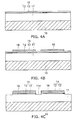
- a method for manufacturing the semiconductor light-emitting device of the embodiment is described below with reference to FIG. 4A to FIG. 10 .
- the first semiconductor layer 11, the light-emitting layer 13, and the second semiconductor layer 12 are epitaxially grown on the major surface of a substrate 10 in order, by using, for example, the MOCVD (metal organic chemical vapor deposition) technique.
- MOCVD metal organic chemical vapor deposition
- the substrate 10 is, for example, a silicon substrate.
- the substrate 10 may be a sapphire substrate.
- the semiconductor layer 15 is, for example, a nitride semiconductor layer containing gallium nitride (GaN).
- the first semiconductor layer 11 has, for example, a buffer layer provided on the major surface of the substrate 10, and an n-type GaN layer provided on the buffer layer.
- the second semiconductor layer 12 has, for example, a p-type GaN layer.
- the light-emitting layer 13 has, for example, an MQW (multiple quantum well) structure.
- the p-side electrode 16 is selectively formed on the semiconductor layer 12, as shown in FIG. 4B .
- the second semiconductor layer 12 and the light-emitting layer 13 are removed by selective etching to selectively expose the first semiconductor layer 11, using, for example, RIE (reactive ion etching) with a mask (not shown).
- RIE reactive ion etching
- the first semiconductor layer 11 is selectively removed to form grooves 61.
- the grooves 61 isolate the semiconductor layers 15 from one another on the major surface of the substrate 10.
- the grooves 61 are formed, for example, in a grid pattern on the wafer of the substrate 10.
- the grooves 61 reach the substrate 10 through the semiconductor layer 15.
- the major surface of the substrate 10 is slightly etched so that the bottom of the grooves 61 is below the interface between the substrate 10 and the first semiconductor layer 11.
- the insulating film 18 is formed so as to cover the structure on the substrate 10.
- the insulating film 18 has openings that are selectively formed, for example, by etching using a resist mask.
- the openings expose the side face 11b of the first semiconductor layer 11, and the first n-side region 11d.
- the openings also partially expose the second n-side region 11c of the first semiconductor layer 11 provided between the side face 11b of the first semiconductor layer 11 and the stacked film 14.
- the insulating film 18 covers the upper surface of the p-side electrode 16, the side face of the p-side electrode 16, and the side face of the stacked film 14.
- the insulating film 18 also covers the bottom surface of the grooves 61.
- the side face 11b of the first semiconductor layer 11 are not aligned with the side face of the stacked film 14.
- the step difference between the side face 11b of the first semiconductor layer 11 and the side face of the stacked film 14 makes it easier to expose the side face 11b of the first semiconductor layer 11 with the insulating film 18 covering the side face of the stacked film 14.
- a resist film 62 is selectively formed on the insulating film 18, and the n-side electrode 17 is formed on the resist film 62, and on the insulating film 18 in portions not covered by the resist film 62.
- the n-side electrode 17 is formed in contact with the side face 11b of the first semiconductor layer 11.
- the n-side electrode 17 is formed in the first n-side region 11d and in the second n-side region 11c.
- the resist film 62 is removed after forming the n-side electrode 17.
- the n-side electrode 17 covering the resist film 62 is removed with the resist film 62.
- the n-side electrode 17 is lifted off with the resist film 62.
- the first portion 17a, the second portion 17c, the third portion 17e (see FIG. 2B ), the fourth portion 17b, and the contact portion 17d of the n-side electrode 17 remain.
- the insulating film 19 is formed on the n-side electrode 17 and on the insulating film 18, as shown in FIG. 7A .
- the opening 82 that exposes the contact portion 17d of the n-side electrode 17 is formed in the insulating film 19.
- the plurality of openings 81 that exposes the p-side electrode 16 is formed in the insulating films 18 and 19 on the p-side electrode 16.
- the p-side interconnection layer 21 and the n-side interconnection layer 22 are formed on the insulating film 19 by using electrolytic copper plating with a resist mask (not shown).
- the p-side interconnection layer 21 is also formed in the openings 81, and is electrically connected to the p-side electrode 16.
- the n-side interconnection layer 22 is also formed in the opening 82, and is electrically connected to the contact portion 17d of the n-side electrode 17.
- the p-side metal pillar 23 and the n-side metal pillar 24 are formed by electrolytic copper plating with a resist mask (not shown), using the p-side interconnection layer 21 and the n-side interconnection layer 22 as seed layers.
- the p-side metal pillar 23 is formed on the p-side interconnection layer 21.
- the p-side interconnection layer 21 and the p-side metal pillar 23 are formed as an integral unit using the same copper material.
- the n-side metal pillar 24 is formed on the n-side interconnection layer 22.
- the n-side interconnection layer 22 and the n-side metal pillar 24 are formed as an integral unit using the same copper material.
- the resin layer ( FIG. 8 ) is formed on the structure shown in FIG. 7B .
- the resin layer 25 covers the p-side interconnection portion 41 including the p-side interconnection layer 21 and the p-side metal pillar 23, and the n-side interconnection portion 43 including the n-side interconnection layer 22 and the n-side metal pillar 24.
- the resin layer 25 is also formed at the periphery portion of the chip, and covers the first portion 17a of the n-side electrode 17 via the insulating film 19.
- the supporting body 100 is configured from the resin layer 25, together with the p-side interconnection portion 41 and the n-side interconnection portion 43.
- the substrate 10 is removed from the semiconductor layer 15 being supported by the supporting body 100.
- the substrate 10 (silicon substrate) is removed by, for example, wet etching or dry etching.
- the substrate may be removed by using a laser lift-off technique.
- the semiconductor layer 15 epitaxially grown on the substrate 10 may have large internal stress.
- the p-side metal pillar 23, the n-side metal pillar 24, and the resin layer 25 are softer than the semiconductor layer 15 of GaN material, and can thus absorb stress even when the internal stress caused by the epitaxial growth is released at once during delamination. The semiconductor layer 15 is thus not damaged in the process of removing the substrate 10.
- the removal of the substrate 10 exposes the first face 11a of the first semiconductor layer 11, as shown in FIG. 9 .
- Microasperities are formed on the exposed first face 11a, as shown in FIG. 10 .
- the first face 11a is wet etched with an etchant such as a KOH (potassium hydroxide) aqueous solution, and TMAH (tetramethylammonium hydroxide).
- KOH potassium hydroxide
- TMAH tetramethylammonium hydroxide
- the etching involves a crystal-face dependent difference in etching rate, and this difference in etching rate enables formation of asperities on the first face 11a.
- the microasperities formed on the first face 11a can improve the extraction efficiency of radiant rays from the light-emitting layer 13.
- Microasperities also may be formed on the first face 11a by dry etching with a resist mask.
- the fluorescent material layer 30 is formed on the first face 11a via the insulating film 51, as shown in FIG. 1 .
- the insulating film 51 is also formed on the insulating film 18 at the outer periphery of the chip.
- the fluorescent material layer 30 is formed by using methods such as printing, potting, molding, and compression molding.
- the insulating film 51 improves the adhesion between the first semiconductor layer 11 and the fluorescent material layer 30.
- the insulating film 51 is, for example, an inorganic insulating film such as a silicon oxide film, a silicon nitride film, and a silicon oxynitride film.
- a fired fluorescent material obtained by firing fluorescent materials with a binder may be bonded to the insulating film 51 to form the fluorescent material layer 30.
- the surface of the resin layer 25, which is the lower surface in FIG. 10 is ground to expose the p-side metal pillar 23 and the n-side metal pillar 24 from the resin layer 25.
- the exposed surface of the p-side metal pillar 23 becomes the p-side external terminal 23a
- the exposed surface of the n-side metal pillar 24 becomes the n-side external terminal 24a.
- the wafer is cut at the regions where the grooves 61 isolating the semiconductor layers 15 are formed.
- a dicing blade, or a laser beam is used.
- the semiconductor layer 15 does not exist in the dicing regions, and is not damaged by dicing.
- the foregoing steps that precede the cutting of the wafer into individual devices are performed on the wafer containing the semiconductor layers 15.
- the wafer is cut into individual semiconductor light-emitting devices to include at least one semiconductor layer 15.
- the semiconductor light-emitting devices may be of a single chip structure with a single semiconductor layer 15, or of a multi chip structure with a plurality of semiconductor layers 15.
- the side face of the fluorescent material layer 30 are in line with the side face of the supporting body 100 (side face of the resin layer 25), and these side face form the side face of each individual semiconductor light-emitting device. This, combined with the absence of substrate 10, enables providing of a small semiconductor light-emitting device of a chip-size package.
- the first portion 17a of the n-side electrode 17 may contact only the side face 11b, without contacting the second n-side region 11c of the first semiconductor layer 11.
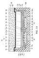
- FIG. 12 is a schematic cross sectional view of another specific example of the semiconductor light-emitting device of the embodiment.
- a transparent electrode 71 for example, such as ITO (indium tin oxide) is provided on the first face 11a that is continuous to the side face 11b of the first semiconductor layer 11.
- the transparent electrode 71 is connected to the first portion 17a of the n-side electrode 17.
- the transparent electrode 71 is in contact with the inner walls at the end portions of the first portion 17a on the first face 11a side.
- the insulating film 72 is provided between the transparent electrode 71 and the fluorescent material layer 30 to improve adhesion between these two components.
- the insulating film 72 is, for example, an inorganic insulating film such as a silicon oxide film, and a silicon nitride film.
- the uniformity of the current through the first semiconductor layer 11 can be further improved in plane direction.
- the major surface of the substrate 10 becomes slight recessed when forming the grooves 61 that isolate the first semiconductor layers 11, as described above with reference to FIG. 5A . Accordingly, as shown in FIG. 6B , the end portions of the first portion 17a of the n-side electrode 17 project out toward the substrate 10 away from the first face 11a of the first semiconductor layer 11 upon forming the first portion 17a on the side face of the grooves 61.
- the substrate 10 is removed, and the first face 11a is roughened as shown in FIG. 10 . This exposes the inner walls of the first portion 17a of the n-side electrode 17 at the end portions. A transparent electrode 71 can then be formed on the first face 11a in this state to contact the transparent electrode 71 to the end portions of the first portion 17a.
- FIG. 13 is a schematic cross sectional view of yet another example of the semiconductor light-emitting device of the embodiment.
- the insulating film (inorganic insulating film) 18 at the outer periphery of the chip does not extend to the side face of the semiconductor light-emitting device.
- the insulating film 18 provided at the outer periphery of the chip is covered with the resin layer 25, and the resin layer 25 forms the side face of the semiconductor light-emitting device.
- the insulating film 18 does not exist in the dicing regions of the diced wafer. This prevents cracking as might occur at the interface between the insulating film 18 and the fluorescent material layer 30 or between the insulating film 18 and the resin layer 25 under the impact of dicing. Entry of moisture through such cracks can thus be prevented to improve the reliability of the semiconductor light-emitting device.
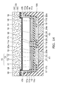
- FIG. 14 is a schematic cross sectional view of still another example of the semiconductor light-emitting device of the embodiment.
- the n-side electrode 17 has a fifth portion 17f provided between the resin layer 25 and the fluorescent material layer 30 at the outer periphery of the chip.
- the fifth portion 17f is integrally provided at the end portions of the first portion 17a provided on the side face 11b of the first semiconductor layer 11, and extends toward the side face of the semiconductor light-emitting device from the end portions of the first portion 17a.
- the light emitted from the fluorescent materials 31 at the chip outer periphery of the semiconductor light-emitting device down toward the supporting body 100 can thus be reflected at the fifth portion 17f of the n-side electrode 17 back toward the fluorescent material layer 30.
- the insulating film 18 provided between the fifth portion 17f and the fluorescent material layer 30 improves the adhesion between these two components.
Landscapes
- Led Devices (AREA)
- Led Device Packages (AREA)
Abstract
Description
- Embodiments described herein relate generally to a semiconductor light-emitting device.
- Electrodes do not interfere with extraction of light from a light-emitting surface in a structure in which a p-side electrode and an n-side electrode are formed on one side of a semiconductor layer including a light-emitting layer. Such a structure offers a high degree of freedom in electrode profile and layout. Electrode profile and layout affect electrical characteristics and luminous efficiency, and require appropriate design.
-
-
FIG. 1 is a schematic cross sectional view of a semiconductor light-emitting device of an embodiment; -
FIGS. 2A and 2B are schematic plan views of the semiconductor light-emitting device of the embodiment; -
FIGS. 3A to 3C are schematic plan views of the semiconductor light-emitting device of the embodiment; -
FIGS. 4A to 10 are schematic cross sectional views showing a method for manufacturing the semiconductor light-emitting device of the embodiment; -
FIG. 11 is a schematic cross sectional view of a semiconductor light-emitting device of the embodiment; -
FIG. 12 is a schematic cross sectional view of a semiconductor light-emitting device of the embodiment; -
FIG. 13 is a schematic cross sectional view of a semiconductor light-emitting device of the embodiment; and -
FIG. 14 is a schematic cross sectional view of a semiconductor light-emitting device of the embodiment. - According to one embodiment, a semiconductor light-emitting device includes a semiconductor layer, a p-side electrode, an insulating film, an n-side electrode, a p-side interconnection portion, and an n-side interconnection portion. The semiconductor layer includes a first semiconductor layer, a second semiconductor layer, and a light-emitting layer provided between the first semiconductor layer and the second semiconductor layer. The first semiconductor layer has a first n-side region surrounded by a stacked film including the light-emitting layer and the second semiconductor layer. The p-side electrode is provided on the second semiconductor layer. The insulating film is provided on the p-side electrode. The n-side electrode includes a first portion, a second portion, and a third portion. The first portion is provided on a side face of the first semiconductor layer. The second portion is provided in the first n-side region. The third portion overlaps the p-side electrode via the insulating film and connects the first portion and the second portion to each other. The p-side interconnection portion is provided on the insulating film and connected to the p-side electrode. The n-side interconnection portion is provided on the insulating film and connected to the n-side electrode.
- Embodiments are described below with reference to the accompanying drawings. In the appended figures, the same components have the same reference numeral.
-
FIG. 1 is a schematic cross sectional view of a semiconductor light-emitting device of the embodiment. -
FIG. 2A is a schematic plan view showing an example of a planar layout of afirst semiconductor layer 11 and asecond semiconductor layer 12 shown inFIG. 1 . -
FIG. 2B is a schematic plan view showing an example of a planar layout of a p-side electrode 16 and an n-side electrode 17 shown inFIG. 1 . - The semiconductor light-emitting device of the embodiment includes a supporting
body 100, afluorescent material layer 30, and a stacked body including asemiconductor layer 15 and provided between the supportingbody 100 and thefluorescent material layer 30. - The
semiconductor layer 15 includes thefirst semiconductor layer 11, thesecond semiconductor layer 12, and a light-emitting layer 13 provided between thefirst semiconductor layer 11 and thesecond semiconductor layer 12. - The
first semiconductor layer 11 and thesecond semiconductor layer 12 contain, for example, gallium nitride (GaN). Thefirst semiconductor layer 11 includes, for example, a foundation buffer layer, and an n-type GaN layer. Thesecond semiconductor layer 12 includes, for example, a p-type GaN layer. The light-emittinglayer 13 contains materials that emit light of different wavelengths, including blue, purple, bluish purple, and ultraviolet light. The emission peak wavelength of the light-emittinglayer 13 occurs between, for example, 430 and 470 nm. - The
first semiconductor layer 11 has afirst face 11a, and aside face 11b that are continuous from thefirst face 11a. Thefirst face 11a is roughened, and has a plurality of microirregularities. - A stacked film (mesa) 14 of the light-emitting
layer 13 and thesecond semiconductor layer 12 is provided on the side of thefirst semiconductor layer 11 opposite thefirst face 11a. The stacked film (mesa) 14 is provided on the opposite side of thefirst face 11a. - The portion including the
stacked film 14, a first n-side region 11d, and a second n-side region 11c are provided on the side of thefirst semiconductor layer 11 opposite thefirst face 11a. Thestacked film 14 having the light-emittinglayer 13 is not provided in the first n-side region 11d and the second n-side region 11c. - As shown in
FIG. 2A , the first n-side region 11d is provided in, for example, an island-like (dot-like) pattern at a planar central portion of thesemiconductor layer 15. The first n-side region 11d is continuously surrounded by thestacked film 14. - The second n-
side region 11c is provided at the outer periphery side thefirst semiconductor layer 11, and, as shown inFIG. 1 , is provided between theside face 11b of thefirst semiconductor layer 11 and thestacked film 14. As shown inFIG. 2A , the second n-side region 11c continuously surrounds thestacked film 14. - As shown in
FIG. 1 , the p-side electrode 16 is provided on thesecond semiconductor layer 12 of thestacked film 14. The p-side electrode 16 is not provided in the first n-side region 11d and the second n-side region 11c. - The n-
side electrode 17 is provided on theside face 11b, and in the first n-side region 11d and the second n-side region 11c of thefirst semiconductor layer 11. The n-side electrode 17 has afirst portion 17a, asecond portion 17c, athird portion 17e, afourth portion 17b, and acontact portion 17d. Thefirst portion 17a, thesecond portion 17c, thethird portion 17e, thefourth portion 17b, and thecontact portion 17d are integrally formed with the same material. Thefirst portion 17a, thesecond portion 17c, thethird portion 17e, thefourth portion 17b, and thecontact portion 17d are continuous with the same material. - The
first portion 17a is provided on theside face 11b of thefirst semiconductor layer 11. Thefirst portion 17a is provided on all of the side faces 11b of thefirst semiconductor layer 11, and continuously surrounds theside faces 11b. Thefirst portion 17a is also provided in a part of the second n-side region 11c that is continuous from theside face 11b. Thefirst portion 17a is in contact with theside face 11b and the second n-side region 11c. - The
first portion 17a projects out of theside face 11b on the opposite side from thefirst face 11a. Thefourth portion 17b is integral with thefirst portion 17a at the leading end of the projection. As shown inFIG. 2B , thefourth portion 17b is provided along the outer periphery of the p-side electrode 16. - As shown in
FIG. 1 , the stackedfilm 14 and the p-side electrode 16 are covered with an insulatingfilm 18. The insulatingfilm 18 is, for example, an inorganic insulating film such as a silicon oxide film. - The
fourth portion 17b overlaps the end portion of the p-side electrode 16 via the insulatingfilm 18. Thefourth portion 17b is, for example, an integral unit of four portions provided along the outer periphery of the p-side electrode 16. - The insulating
film 18 is provided between the n-side electrode 17 and the stackedfilm 14, and between the n-side electrode 17 and the p-side electrode 16. - The
second portion 17c of the n-side electrode 17 is provided in the first n-side region 11d of thefirst semiconductor layer 11. Thesecond portion 17c is in contact with thefirst semiconductor layer 11 in the first n-side region 11d. - The
first portion 17a and thesecond portion 17c are connected to each other via thefourth portion 17b and thethird portion 17e (seeFIG. 2B ). - As shown in
FIG. 2B , thethird portion 17e connects two parallel portions in the four portions of thefourth portion 17b across the p-side electrode 16. Thethird portion 17e overlaps the p-side electrode 16 via the insulatingfilm 18, and connects thefirst portion 17a and thesecond portion 17c to each other. - The
contact portion 17d is provided on one of the fourfourth portions 17b. Thecontact portion 17d projects out in a width direction of thefourth portion 17b. Thecontact portion 17d overlaps the p-side electrode 16 via the insulatingfilm 18. - The n-
side electrode 17 includes a first film (for example, an aluminum film) that makes ohmic contact with the first semiconductor layer (for example, an n-type GaN layer) 11. The aluminum film has reflectivity for light emitted by the light-emittinglayer 13. The n-side electrode 17 also includes a second film (for example, a titanium film, a platinum film, a gold film, or a nickel film) stacked on the first film (aluminum film). - The p-
side electrode 16 includes a first film (for example, a silver film) that makes ohmic contact with the second semiconductor layer (for example, a p-type GaN layer) 12. The silver film has reflectivity for light emitted by the light-emittinglayer 13. The p-side electrode 16 also includes a second film (for example, a titanium film, a platinum film, a gold film, or a nickel film) stacked on the first film (silver film). - The light-emitting
layer 13 emits light with the current supplied thereto through the p-side electrode 16 and the n-side electrode 17. The light from the light-emittinglayer 13 enters into thefluorescent material layer 30 from thefirst face 11a side of thefirst semiconductor layer 11. - An area of the light-emitting region including the light-emitting layer 13 (the region where the p-
side electrode 16 is provided) is larger than an area of the n-side region (the first n-side region 11d and the second n-side region 11c) not including the light-emittinglayer 13. This makes it possible to provide a large light-emitting surface, and increase the light output. - The supporting
body 100 is provided on the side of thesemiconductor layer 15 opposite thefirst face 11a (second face side). The supportingbody 100 supports the light-emitting element including thesemiconductor layer 15, the p-side electrode 16, and the n-side electrode 17. - The
fluorescent material layer 30 is provided on thefirst face 11a side of thesemiconductor layer 15 as an optical layer that confers the desired optical characteristics to light emitted from thesemiconductor layer 15. Thefluorescent material layer 30 contains a plurality of particulatefluorescent materials 31. Thefluorescent materials 31 are excited by light emitted from the light-emittinglayer 13, and emit light of wavelength different from the wavelength of the light emitted from the light-emittinglayer 13. - The
fluorescent materials 31 are dispersed in atransparent layer 32. Thetransparent layer 32 transmits the light emitted from the light-emittinglayer 13 and the light emitted from thefluorescent materials 31. The term "transparent" is not limited to 100% transmittance, and encompasses absorption of some of the light. - The p-
side electrode 16 and the n-side electrode 17 are covered with the insulatingfilms semiconductor layer 15 opposite thefirst face 11a (second face side). The insulatingfilms - A p-
side interconnection layer 21 and an n-side interconnection layer 22 are separately provided on the insulatingfilms - As shown in
FIG. 7A , the insulatingfilms first openings 81 connecting to the p-side electrode 16, and asecond opening 82 connecting to thecontact portion 17d of the n-side electrode 17. Thefirst openings 81 may be provided as a single larger opening. - The p-
side interconnection layer 21 is provided inside thefirst openings 81, and on the insulatingfilms side interconnection layer 21 is electrically connected to the p-side electrode 16 via a plurality ofvias 21a inside thefirst openings 81. - The n-
side interconnection layer 22 is provided inside thesecond opening 82, and on the insulatingfilms side interconnection layer 22 is electrically connected to thecontact portion 17d of the n-side electrode 17 via a via 22a inside thesecond opening 82. - The p-
side interconnection layer 21 partially overlaps thethird portion 17e of the n-side electrode 17 via the insulatingfilm 19 on the side of the n-side interconnection layer 22. Other portion of the p-side interconnection layer 21 overlaps thefourth portion 17b of the n-side electrode 17 via the insulatingfilm 19. The n-side interconnection layer 22 overlaps the p-side electrode 16 via the insulatingfilms - The p-
side interconnection layer 21 and the n-side interconnection layer 22 include, for example, a copper film. The copper film is formed on a foundation metal film by, for example, plating. The foundation metal film includes a copper film that becomes a seed layer for plating, and, for example, an aluminum film having high reflectivity for light emitted from the light-emittinglayer 13. The foundation metal film also includes a titanium film or a titanium nitride film provided between the copper film and the aluminum film. The titanium film or the titanium nitride film serves as a barrier film and an adhesive film. - The p-
side interconnection layer 21 and the n-side interconnection layer 22 spread over the insulatingfilms semiconductor layer 15. The aluminum layer in the foundation of the p-side interconnection layer 21 and the n-side interconnection layer 22 is formed over large portions of the region on the second face side of thesemiconductor layer 15. This enables an increase in the quantity of light directed to thefluorescent material layer 30. - The n-
side electrode 17 having the aluminum film is also provided on theside face 11b of thefirst semiconductor layer 11. The light directed to theside face 11b of thefirst semiconductor layer 11 from the light-emittinglayer 13 is reflected at the n-side electrode 17, and does not leak to outside. This enables prevention of color breakup or unevenness due to leakage of light from the side face of the semiconductor light-emitting device. - A p-
side metal pillar 23 is provided on the p-side interconnection layer 21. A p-side interconnection portion 41 includes the p-side interconnection layer 21 and the p-side metal pillar 23. An n-side metal pillar 24 is provided on the n-side interconnection layer 22. An n-side interconnection portion 43 includes the n-side interconnection layer 22 and the n-side metal pillar 24. - A
resin layer 25 is provided as an insulating layer between the p-side interconnection portion 41 and the n-side interconnection portion 43. Theresin layer 25 is provided on the side face of the p-side interconnection portion 41 and on the side face of the n-side interconnection portion 43. Theresin layer 25 is filled between the p-side metal pillar 23 and the n-side metal pillar 24, in contact with the side face of the p-side metal pillar 23 and the side face of the n-side metal pillar 24. Theresin layer 25 is also filled between the p-side interconnection layer 21 and the n-side interconnection layer 22. - The
resin layer 25 is also provided in a region (chip outer periphery portion) adjacent to theside face 11b of thefirst semiconductor layer 11, and covers thefirst portion 17a of the n-side electrode 17. - The end portion (face) of the p-
side metal pillar 23 opposite the p-side interconnection layer 21 is exposed from theresin layer 25, and serves as a p-side external terminal 23a that is connectable to external circuits such as a mounting substrate. The end portion (face) of the n-side metal pillar 24 opposite the n-side interconnection layer 22 is exposed from theresin layer 25, and serves as an n-side external terminal 24a that is connectable to external circuits such as a mounting substrate. The p-side external terminal 23a and the n-side external terminal 24a are bonded to pads of a mounting substrate via, for example, a solder or a conductive bonding material. - The distance between the p-side external terminal 23a and the n-side external terminal 24a is longer than the distance between the p-
side interconnection layer 21 and the n-side interconnection layer 22 on the insulatingfilm 19. The p-side external terminal 23a and the n-side external terminal 24a are spaced apart from each other by a distance that is wider than the spread area of a solder used for mounting. This can prevent the solder from shorting the p-side external terminal 23a and the n-side external terminal 24a. - On the other hand, the p-
side interconnection layer 21 and the n-side interconnection layer 22 can be brought as close to each other as the processing limit allows. This makes it possible to increase the area of the p-side interconnection layer 21, and thereby promote radiation of heat of the light-emittinglayer 13. - The contact area of the p-
side interconnection layer 21 and the p-side electrode 16 via the plurality ofvias 21a is larger than the contact area of the n-side interconnection layer 22 and the n-side electrode 17 via the via 22a. In this way, a uniform current distribution can be ensured through the light-emittinglayer 13. - The area of the n-
side interconnection layer 22 spread on the insulatingfilms side region 11d and the second n-side region 11c. The area of the n-side external terminal 24a of the n-side metal pillar 24 provided on the n-side interconnection layer 22 can be made larger than the areas of the first n-side region 11d and the second n-side region 11c. In this way, the areas of the first n-side region 11d and the second n-side region 11c can be made smaller while providing a sufficiently large area for the n-side external terminal 24a to enable reliable mounting. Thesemiconductor layer 15 can have a smaller area in regions excluding the light-emittinglayer 13, and the area of the light-emitting region having the light-emittinglayer 13 can be increased to improve the light output. - The
first semiconductor layer 11 is electrically connected to the n-side metal pillar 24 via the n-side electrode 17 and the n-side interconnection layer 22. Thesecond semiconductor layer 12 is electrically connected to the p-side metal pillar 23 via the p-side electrode 16 and the p-side interconnection layer 21. - The thickness of the p-side metal pillar 23 (the thickness from the p-
side interconnection layer 21 to the p-side external terminal 23a) is larger than the thickness of the p-side interconnection layer 21. The thickness of the n-side metal pillar 24 (the thickness from the n-side interconnection layer 22 to the n-side external terminal 24a) is larger than the thickness of the n-side interconnection layer 22. The p-side metal pillar 23, the n-side metal pillar 24, and theresin layer 25 are thicker than thesemiconductor layer 15. - The aspect ratio of the
metal pillars 23 and 24 (the thickness ratio with respect to planar size) may be 1 or more, or less than 1. Themetal pillars - The thickness of the supporting
body 100 including the p-side interconnection layer 21, the n-side interconnection layer 22, the p-side metal pillar 23, the n-side metal pillar 24, and theresin layer 25 is thicker than the thickness of the light-emitting element (LED chip) including thesemiconductor layer 15, the p-side electrode 16, and the n-side electrode 17. - The
semiconductor layer 15 is formed on a substrate by using the epitaxial growth. The substrate is removed after forming the supportingbody 100, and the substrate is not provided on thefirst face 11a side of thesemiconductor layer 15. Thesemiconductor layer 15 is supported not by a rigid plate substrate, but by the supportingbody 100 composed of themetal pillars resin layer 25. - The p-
side interconnection portion 41 and the n-side interconnection portion 43 may be made of materials, for example, such as copper, gold, nickel, and silver. Heat conductivity, migration resistance, and adhesion for the insulating material can be improved by using copper. - The
resin layer 25 reinforces the p-side metal pillar 23 and the n-side metal pillar 24. Theresin layer 25 is desirably made of materials having the same or similar coefficient of thermal expansion as the mounting substrate. Examples of such materials for theresin layer 25 include resins of primarily epoxy resin, resins of primarily silicone resin, and resins of primarily fluororesin. - The base resin in the
resin layer 25 contains additives such as a light absorbing agent, a light reflecting agent, and a light scattering agent, making theresin layer 25 lightproof or reflective for light from the light-emittinglayer 13. This enables reduction of leakage of light from the side face and the mounting surface side of the supportingbody 100. - Because of the heat cycle during the mounting of the semiconductor light-emitting device, the
semiconductor layer 15 is subjected to stress due to such factors as soldering of the p-side external terminal 23a and the n-side external terminal 24a to the pads of the mounting substrate. The p-side metal pillar 23, the n-side metal pillar 24, and theresin layer 25 absorb and relieve such stress. Theresin layer 25, softer than thesemiconductor layer 15 and used as a part of the supportingbody 100 particularly improves the stress relieving effect. - The substrate used for the formation (growth) of the
semiconductor layer 15 is removed from thesemiconductor layer 15. This reduces the height of the semiconductor light-emitting device. It also becomes possible to form microirregularities on thefirst face 11a after the removal of the substrate from this surface of thesemiconductor layer 15, and improve the efficiency at which light can be extracted. For example, wet etching with an alkaline solution, or dry etching is used to form microirregularities, and the rough surface (first face 11a) is formed on the light extracting side of thesemiconductor layer 15. The rough surface can reduce the total reflection component, and improve the light extraction efficiency. - The
fluorescent material layer 30 is formed on the roughenedfirst face 11a via an insulatingfilm 51. The insulatingfilm 51 serves as an adhesive layer to improve the adhesion between thesemiconductor layer 15 and thefluorescent material layer 30. For example, the insulatingfilm 51 is an inorganic film such as a silicon oxide film or a silicon nitride film. - The
fluorescent material layer 30 has a structure in which theparticulate fluorescent materials 31 are dispersed in thetransparent layer 32. Thetransparent layer 32 is, for example, a transparent resin layer of primarily silicone resin. - The
fluorescent material layer 30 spreads to the outer periphery of the chip from thefirst face 11a. The insulatingfilm 18, serving as an adhesive layer, is provided between theresin layer 25 and thefluorescent material layer 30, and between the n-side electrode 17 and thefluorescent material layer 30 at the outer periphery of the chip. - The
fluorescent material layer 30 does not cover or surround the second face side of thesemiconductor layer 15, themetal pillars body 100. The side face of thefluorescent material layer 13 is aligned with the side face of the supporting body 100 (side face of the resin layer 25). - That is, the semiconductor light-emitting device of the embodiment is a very small device of a chip-size package structure. This improves the freedom of lamp fitting design in applications, for example, such as lamp fittings for lighting.
- Cost also can be reduced because the
fluorescent material layer 30 is not unnecessarily formed on the mounting face side where light is not extracted to outside. The device also allows the heat of the light-emittinglayer 13 to be released to the mounting substrate side via the p-side interconnection layer 21, the n-side interconnection layer 22, and themetal pillars - In common flip-chip mounting, the fluorescent material layer is formed over the whole LED chip after the chip is mounted on a mounting substrate via bumps or the like. Alternatively, resin is underfilled between bumps.
- In contrast, in the embodiment, the
resin layer 25, different from thefluorescent material layer 30, has already been provided around the p-side metal pillar 23 and the n-side metal pillar 24 at the time of mounting, and the mounting surface side can have properties suited for relieving stress. The provision of theresin layer 25 on the mounting face side prior to mounting also eliminates the need for the post-mounting underfill. - An optical layer of a design that is more oriented toward properties such as light extraction efficiency, color conversion efficiency, and light distribution is provided on the first face (roughed surface) 11a side, whereas a layer that is oriented toward relieving stress during mounting, or providing properties as a substrate-replacing supporting body is provided on the mounting surface side. For example, the
resin layer 25 may be filled with a high density of fillers such as silica particles to appropriately adjust hardness for use as a supporting body. - The light emitted from the light-emitting
layer 13 toward thefirst face 11a side enters into thefluorescent material layer 30, and some of the light excites thefluorescent materials 31. The light from thefluorescent materials 31 mixes with the light from the light-emittinglayer 13, and produces, for example, pseudo white light. - If a substrate is provided on the
first face 11a side, some of the light do not enter into thefluorescent material layer 30 and leak out from the side face of the substrate. Light with the color shifted to the light of the light-emittinglayer 13 leaks out from the side face of the substrate. This may cause color breakup or unevenness. For example, a blue ring may appear at the outer edges when thefluorescent material layer 30 is viewed from above. - In the embodiment, the substrate is absent between the
first face 11a and thefluorescent material layer 30. Color breakage or unevenness caused when light with the color shifted to the light of the light-emittinglayer 13 leaks out from the side face of the substrate can be prevented. - In the embodiment, the contact area of the n-
side electrode 17 and theside face 11b of thefirst semiconductor layer 11 is larger than the total area of the contact area of the n-side electrode 17 and the first n-side region 11d on the second face side of thefirst semiconductor layer 11, and the contact area of the n-side electrode 17 and the second n-side region 11c on the second face side of thefirst semiconductor layer 11. - Because the area of contact between the n-
side electrode 17 and thefirst semiconductor layer 11 is restricted on the second face side of thefirst semiconductor layer 11, the stackedlayer 14 including the light-emittinglayer 13, and the p-side electrode 16 provided in contact with the stackedlayer 14 can spread over a relatively larger area (light-emitting region) on the second face side. The larger light-emitting region improves the light flux of the semiconductor light-emitting device. - It may become difficult to efficiently pass current in the vicinity of the planar center of the light-emitting
layer 13 when the n-side electrode 17 and thefirst semiconductor layer 11 are in contact with each other only at theside face 11b of thefirst semiconductor layer 11. - In the embodiment, the n-
side electrode 17 is in contact with the first n-side region 11d of thefirst semiconductor layer 11 also in the vicinity of the center on the second face side, and current can be uniformly passed through the light-emittinglayer 13. - The embodiment can thus provide a semiconductor light-emitting device that can produce a large flux of uniform light with a uniform current distribution that is achieved despite the large light-emitting region.
- The
second portion 17c of the n-side electrode 17 provided in the first n-side region 11d does not have a contact portion for the n-side interconnection layer 22. Thesecond portion 17c can thus have a reduced width and a reduced area, and the area of the light-emitting region where the light-emittinglayer 13 and the p-side electrode 16 are provided can be relatively increased. - The
contact portion 17d between the n-side electrode 17 and the n-side interconnection layer 22 overlaps the p-side electrode 16 via the insulatingfilm 18. Thecontact portion 17d is not in contact with the second face of thefirst semiconductor layer 11. Thecontact portion 17d thus does not restrict the area of the p-side electrode 16, and the light-emitting region can be increased. - The n-
side electrode 17 is an integral unit of thefirst portion 17a, thesecond portion 17c, thethird portion 17e, thefourth portion 17b, and thecontact portion 17d. Accordingly, the contact between the n-side interconnection layer 22 and the n-side electrode 17 only needs to be made at one location. The n-side interconnection layer 22 does not need to contact each portion of the n-side electrode 17. - The
fourth portion 17b connecting thefirst portion 17a to thethird portion 17e and to thecontact portion 17d overlaps the end portion of the p-side electrode 16 via the insulatingfilm 18. Therefore, the width of thefourth portion 17b can be increased to decrease the overall resistance of the n-side electrode 17, without sacrificing the area of the p-side electrode 16. This makes it possible to increase the efficiency of supplying current to the light-emittinglayer 13, and enable the semiconductor light-emitting device to produce a large flux of uniform light. - As shown in
FIGS. 3A, 3B, and 3C , more than one first n-side region 11d may be provided, and the n-side electrode 17 may have more than onesecond portion 17c. A plurality of first n-side regions 11d is disposed in a dot-like pattern. Thefourth portion 17b at the outer periphery of thesemiconductor layer 15 is connected to thesecond portions 17c with a plurality ofthird portions 17e. - With the plurality of first n-
side regions 11d and the plurality ofsecond portions 17c in the n-side electrode 17, current can be more evenly distributed over the plane of thesemiconductor layer 15. - As shown in
FIG. 3C , thethird portions 17e may have a form of a grid so as to intersect at thesecond portions 17c. - A method for manufacturing the semiconductor light-emitting device of the embodiment is described below with reference to
FIG. 4A to FIG. 10 . - As shown in
FIG. 4A , thefirst semiconductor layer 11, the light-emittinglayer 13, and thesecond semiconductor layer 12 are epitaxially grown on the major surface of asubstrate 10 in order, by using, for example, the MOCVD (metal organic chemical vapor deposition) technique. - The
substrate 10 is, for example, a silicon substrate. Thesubstrate 10 may be a sapphire substrate. Thesemiconductor layer 15 is, for example, a nitride semiconductor layer containing gallium nitride (GaN). - The
first semiconductor layer 11 has, for example, a buffer layer provided on the major surface of thesubstrate 10, and an n-type GaN layer provided on the buffer layer. Thesecond semiconductor layer 12 has, for example, a p-type GaN layer. The light-emittinglayer 13 has, for example, an MQW (multiple quantum well) structure. - The p-
side electrode 16 is selectively formed on thesemiconductor layer 12, as shown inFIG. 4B . - Thereafter, as shown in
FIG. 4C , thesecond semiconductor layer 12 and the light-emittinglayer 13 are removed by selective etching to selectively expose thefirst semiconductor layer 11, using, for example, RIE (reactive ion etching) with a mask (not shown). - This exposes the first n-
side region 11d in a region surrounded by the stacked layer (mesa) 14 including thesecond semiconductor layer 12 and the light-emittinglayer 13, and by the p-side electrode 16. - Thereafter, as shown in
FIG. 5A , thefirst semiconductor layer 11 is selectively removed to formgrooves 61. Thegrooves 61 isolate the semiconductor layers 15 from one another on the major surface of thesubstrate 10. Thegrooves 61 are formed, for example, in a grid pattern on the wafer of thesubstrate 10. - The
grooves 61 reach thesubstrate 10 through thesemiconductor layer 15. The major surface of thesubstrate 10 is slightly etched so that the bottom of thegrooves 61 is below the interface between thesubstrate 10 and thefirst semiconductor layer 11. - Thereafter, as shown in
FIG. 5B , the insulatingfilm 18 is formed so as to cover the structure on thesubstrate 10. The insulatingfilm 18 has openings that are selectively formed, for example, by etching using a resist mask. The openings expose theside face 11b of thefirst semiconductor layer 11, and the first n-side region 11d. The openings also partially expose the second n-side region 11c of thefirst semiconductor layer 11 provided between theside face 11b of thefirst semiconductor layer 11 and the stackedfilm 14. - The insulating
film 18 covers the upper surface of the p-side electrode 16, the side face of the p-side electrode 16, and the side face of the stackedfilm 14. The insulatingfilm 18 also covers the bottom surface of thegrooves 61. - The
side face 11b of thefirst semiconductor layer 11 are not aligned with the side face of the stackedfilm 14. The step difference between theside face 11b of thefirst semiconductor layer 11 and the side face of the stackedfilm 14 makes it easier to expose theside face 11b of thefirst semiconductor layer 11 with the insulatingfilm 18 covering the side face of the stackedfilm 14. - As shown in
FIG. 6A , a resistfilm 62 is selectively formed on the insulatingfilm 18, and the n-side electrode 17 is formed on the resistfilm 62, and on the insulatingfilm 18 in portions not covered by the resistfilm 62. - The n-
side electrode 17 is formed in contact with theside face 11b of thefirst semiconductor layer 11. The n-side electrode 17 is formed in the first n-side region 11d and in the second n-side region 11c. - The resist
film 62 is removed after forming the n-side electrode 17. The n-side electrode 17 covering the resistfilm 62 is removed with the resistfilm 62. The n-side electrode 17 is lifted off with the resistfilm 62. - As shown in
FIG. 6B , thefirst portion 17a, thesecond portion 17c, thethird portion 17e (seeFIG. 2B ), thefourth portion 17b, and thecontact portion 17d of the n-side electrode 17 remain. - The insulating
film 19 is formed on the n-side electrode 17 and on the insulatingfilm 18, as shown inFIG. 7A . Theopening 82 that exposes thecontact portion 17d of the n-side electrode 17 is formed in the insulatingfilm 19. The plurality ofopenings 81 that exposes the p-side electrode 16 is formed in the insulatingfilms side electrode 16. - Thereafter, as shown in
FIG. 7B , the p-side interconnection layer 21 and the n-side interconnection layer 22 are formed on the insulatingfilm 19 by using electrolytic copper plating with a resist mask (not shown). - The p-
side interconnection layer 21 is also formed in theopenings 81, and is electrically connected to the p-side electrode 16. The n-side interconnection layer 22 is also formed in theopening 82, and is electrically connected to thecontact portion 17d of the n-side electrode 17. - Thereafter, the p-
side metal pillar 23 and the n-side metal pillar 24 are formed by electrolytic copper plating with a resist mask (not shown), using the p-side interconnection layer 21 and the n-side interconnection layer 22 as seed layers. - The p-
side metal pillar 23 is formed on the p-side interconnection layer 21. The p-side interconnection layer 21 and the p-side metal pillar 23 are formed as an integral unit using the same copper material. The n-side metal pillar 24 is formed on the n-side interconnection layer 22. The n-side interconnection layer 22 and the n-side metal pillar 24 are formed as an integral unit using the same copper material. - Thereafter, the resin layer (
FIG. 8 ) is formed on the structure shown inFIG. 7B . Theresin layer 25 covers the p-side interconnection portion 41 including the p-side interconnection layer 21 and the p-side metal pillar 23, and the n-side interconnection portion 43 including the n-side interconnection layer 22 and the n-side metal pillar 24. - The
resin layer 25 is also formed at the periphery portion of the chip, and covers thefirst portion 17a of the n-side electrode 17 via the insulatingfilm 19. - The supporting
body 100 is configured from theresin layer 25, together with the p-side interconnection portion 41 and the n-side interconnection portion 43. Thesubstrate 10 is removed from thesemiconductor layer 15 being supported by the supportingbody 100. - The substrate 10 (silicon substrate) is removed by, for example, wet etching or dry etching. When the
substrate 10 is a sapphire substrate, the substrate may be removed by using a laser lift-off technique. - The
semiconductor layer 15 epitaxially grown on thesubstrate 10 may have large internal stress. The p-side metal pillar 23, the n-side metal pillar 24, and theresin layer 25 are softer than thesemiconductor layer 15 of GaN material, and can thus absorb stress even when the internal stress caused by the epitaxial growth is released at once during delamination. Thesemiconductor layer 15 is thus not damaged in the process of removing thesubstrate 10. - The removal of the
substrate 10 exposes thefirst face 11a of thefirst semiconductor layer 11, as shown inFIG. 9 . Microasperities are formed on the exposedfirst face 11a, as shown inFIG. 10 . For example, thefirst face 11a is wet etched with an etchant such as a KOH (potassium hydroxide) aqueous solution, and TMAH (tetramethylammonium hydroxide). The etching involves a crystal-face dependent difference in etching rate, and this difference in etching rate enables formation of asperities on thefirst face 11a. The microasperities formed on thefirst face 11a can improve the extraction efficiency of radiant rays from the light-emittinglayer 13. Microasperities also may be formed on thefirst face 11a by dry etching with a resist mask. - The
fluorescent material layer 30 is formed on thefirst face 11a via the insulatingfilm 51, as shown inFIG. 1 . The insulatingfilm 51 is also formed on the insulatingfilm 18 at the outer periphery of the chip. Thefluorescent material layer 30 is formed by using methods such as printing, potting, molding, and compression molding. The insulatingfilm 51 improves the adhesion between thefirst semiconductor layer 11 and thefluorescent material layer 30. The insulatingfilm 51 is, for example, an inorganic insulating film such as a silicon oxide film, a silicon nitride film, and a silicon oxynitride film. - A fired fluorescent material obtained by firing fluorescent materials with a binder may be bonded to the insulating
film 51 to form thefluorescent material layer 30. - After forming the
fluorescent material layer 30, the surface of theresin layer 25, which is the lower surface inFIG. 10 , is ground to expose the p-side metal pillar 23 and the n-side metal pillar 24 from theresin layer 25. The exposed surface of the p-side metal pillar 23 becomes the p-side external terminal 23a, and the exposed surface of the n-side metal pillar 24 becomes the n-side external terminal 24a. - Thereafter, the wafer is cut at the regions where the
grooves 61 isolating the semiconductor layers 15 are formed. This cuts thefluorescent material layer 30, the insulatingfilms resin layer 25. For example, a dicing blade, or a laser beam is used. Thesemiconductor layer 15 does not exist in the dicing regions, and is not damaged by dicing. - The foregoing steps that precede the cutting of the wafer into individual devices are performed on the wafer containing the semiconductor layers 15. The wafer is cut into individual semiconductor light-emitting devices to include at least one
semiconductor layer 15. The semiconductor light-emitting devices may be of a single chip structure with asingle semiconductor layer 15, or of a multi chip structure with a plurality of semiconductor layers 15. - The foregoing steps that precede the cutting of the wafer into individual devices are all performed in a wafer state, and there is no need to form interconnections or pillars for each individual device, nor does it required to package each device with the resin layer, or form the fluorescent material layer for each device. This greatly reduces cost.
- Because the supporting
body 100 and thefluorescent material layer 30 are cut in the form of a wafer after being formed, the side face of thefluorescent material layer 30 are in line with the side face of the supporting body 100 (side face of the resin layer 25), and these side face form the side face of each individual semiconductor light-emitting device. This, combined with the absence ofsubstrate 10, enables providing of a small semiconductor light-emitting device of a chip-size package. - As shown in
FIG. 11 , thefirst portion 17a of the n-side electrode 17 may contact only theside face 11b, without contacting the second n-side region 11c of thefirst semiconductor layer 11. -
FIG. 12 is a schematic cross sectional view of another specific example of the semiconductor light-emitting device of the embodiment. - In the semiconductor light-emitting device shown in
FIG. 12 , atransparent electrode 71, for example, such as ITO (indium tin oxide) is provided on thefirst face 11a that is continuous to theside face 11b of thefirst semiconductor layer 11. Thetransparent electrode 71 is connected to thefirst portion 17a of the n-side electrode 17. Thetransparent electrode 71 is in contact with the inner walls at the end portions of thefirst portion 17a on thefirst face 11a side. - An insulating
film 72 is provided between thetransparent electrode 71 and thefluorescent material layer 30 to improve adhesion between these two components. The insulatingfilm 72 is, for example, an inorganic insulating film such as a silicon oxide film, and a silicon nitride film. - By the provision of the
transparent electrode 71 connected to the n-side electrode 17 and provided over the whole surface of thefirst face 11a of thefirst semiconductor layer 11, the uniformity of the current through thefirst semiconductor layer 11 can be further improved in plane direction. - The major surface of the
substrate 10 becomes slight recessed when forming thegrooves 61 that isolate the first semiconductor layers 11, as described above with reference toFIG. 5A . Accordingly, as shown inFIG. 6B , the end portions of thefirst portion 17a of the n-side electrode 17 project out toward thesubstrate 10 away from thefirst face 11a of thefirst semiconductor layer 11 upon forming thefirst portion 17a on the side face of thegrooves 61. - The
substrate 10 is removed, and thefirst face 11a is roughened as shown inFIG. 10 . This exposes the inner walls of thefirst portion 17a of the n-side electrode 17 at the end portions. Atransparent electrode 71 can then be formed on thefirst face 11a in this state to contact thetransparent electrode 71 to the end portions of thefirst portion 17a. -
FIG. 13 is a schematic cross sectional view of yet another example of the semiconductor light-emitting device of the embodiment. - In the embodiment shown in
FIG. 13 , the insulating film (inorganic insulating film) 18 at the outer periphery of the chip does not extend to the side face of the semiconductor light-emitting device. The insulatingfilm 18 provided at the outer periphery of the chip is covered with theresin layer 25, and theresin layer 25 forms the side face of the semiconductor light-emitting device. - Accordingly, the insulating
film 18 does not exist in the dicing regions of the diced wafer. This prevents cracking as might occur at the interface between the insulatingfilm 18 and thefluorescent material layer 30 or between the insulatingfilm 18 and theresin layer 25 under the impact of dicing. Entry of moisture through such cracks can thus be prevented to improve the reliability of the semiconductor light-emitting device. -
FIG. 14 is a schematic cross sectional view of still another example of the semiconductor light-emitting device of the embodiment. - In the embodiment shown in
FIG. 14 , the n-side electrode 17 has afifth portion 17f provided between theresin layer 25 and thefluorescent material layer 30 at the outer periphery of the chip. Thefifth portion 17f is integrally provided at the end portions of thefirst portion 17a provided on theside face 11b of thefirst semiconductor layer 11, and extends toward the side face of the semiconductor light-emitting device from the end portions of thefirst portion 17a. - The light emitted from the
fluorescent materials 31 at the chip outer periphery of the semiconductor light-emitting device down toward the supportingbody 100 can thus be reflected at thefifth portion 17f of the n-side electrode 17 back toward thefluorescent material layer 30. - This makes it possible to prevent the loss of light from the
fluorescent materials 31 due to absorption by theresin layer 25 at the chip outer periphery of the semiconductor light-emitting device, and improve the efficiency of extracting light from thefluorescent material layer 30 side. - The insulating
film 18 provided between thefifth portion 17f and thefluorescent material layer 30 improves the adhesion between these two components. - While certain embodiments have been described, these embodiments have been presented by way of example only, and are not intended to limit the scope of the inventions. Indeed, the novel embodiments described herein may be embodied in a variety of other forms; furthermore, various omissions, substitutions and changes in the form of the embodiments described herein may be made without departing from the spirit of the inventions. The accompanying claims and their equivalents are intended to cover such forms or modification as would fall within the scope and spirit of the inventions.
Claims (20)
- A semiconductor light-emitting device, comprising:a semiconductor layer (15) including a first semiconductor layer (11), a second semiconductor layer (12), and a light-emitting layer (13) provided between the first semiconductor layer (11) and the second semiconductor layer (12), the first semiconductor layer (11) having a first n-side region (11d) surrounded by a stacked film (14) including the light-emitting layer (13) and the second semiconductor layer (12);a p-side electrode (16) provided on the second semiconductor layer (12);an insulating film (18) provided on the p-side electrode (16);an n-side electrode (17) including a first portion (17a), a second portion (17c), and a third portion (17e), the first portion (17a) provided on a side face (11b) of the first semiconductor layer (11), the second portion (17c) provided in the first n-side region (11d), the third portion (17e) overlapping the p-side electrode (16) via the insulating film (18) and connecting the first portion (17a) and the second portion (17c) to each other;a p-side interconnection portion (41) provided on the insulating film (18) and connected to the p-side electrode (16); andan n-side interconnection portion (43) provided on the insulating film (18) and connected to the n-side electrode (17).
- The device according to claim 1, wherein the n-side electrode (17) has a fourth portion (17b) provided along an outer periphery of the p-side electrode (16).
- The device according to claim 2, wherein the fourth portion (17b) overlaps an end portion of the p-side electrode (16) via the insulating film (18).
- The device according to claim 2 or 3, wherein the fourth portion (17b) is connected to the third portion (17e).
- The device according to any of claims 2-4, wherein the n-side electrode (17) includes a contact portion (17d) integrally provided with the fourth portion (17b), and
the n-side interconnection portion (43) is connected to the contact portion (17d). - The device according to claim 5, wherein the contact portion (17d) overlaps the p-side electrode (16) via the insulating film (18).
- The device according to any of claims 1-6, wherein the n-side electrode (17) includes an aluminum film in contact with the first semiconductor layer (11).
- The device according to any of claims 1-7, wherein the p-side electrode (16) includes a silver film in contact with the second semiconductor layer (12).
- The device according to any of claims 1-8, wherein the n-side electrode (17) contacts the first semiconductor layer (11) at the first portion (17a) and at the second portion (17c).
- The device according to claim 1, wherein the first portion (17a), the second portion (17c), and the third portion (17e) of the n-side electrode (17) are integrally formed with a same material.
- The device according to claim 2, wherein the first portion (17a), the second portion (17c), the third portion (17e), and the fourth portion (17b) of the n-side electrode (17) are integrally formed with a same material.
- The device according to any of claims 1-11, wherein
the first semiconductor layer (11) has a second n-side region (11c) provided between the side face (11b) and the stacked film (14); and
the first portion (17a) of the n-side electrode (17) is also provided in the second n-side region (11c). - The device according to claim 12, wherein a contact area of the n-side electrode (17) and the side face (11b) of the first semiconductor layer (11) is larger than a total area of a contact area of the n-side electrode (17) and the first n-side region (11d), and a contact area of the n-side electrode (17) and the second n-side region (11c).
- The device according to any of claims 1-13, wherein a plurality of first n-side regions (11d) is disposed in a dot-like pattern.
- The device according to any of claims 1-14, further comprising a transparent electrode (71) provided on a first face (11a) continuous to the side face (11b) of the first semiconductor layer (11), and connected to the first portion (17a) of the n-side electrode (17).
- The device according to claim 15, wherein
the first portion (17a) of the n-side electrode (17) has an end portion projecting out from the first face (11a) of the first semiconductor layer (11); and
the transparent electrode (71) is in contact with the end portion of the first portion (17a). - The device according to any of claims 1-16, further comprising a fluorescent material layer (30) provided on the first semiconductor layer (11) without a substrate (10) interposed between the fluorescent material layer (30) and the first semiconductor layer (11).
- The device according to claim 17, further comprising an inorganic film (51) provided between the first semiconductor layer (11) and the fluorescent material layer (30).
- The device according to any of claims 1-18, wherein
the p-side interconnection portion (41) includes a p-side interconnection layer (21) connected to the p-side electrode (16), and a p-side metal pillar (23) provided on the p-side interconnection layer (21) and thicker than the p-side interconnection layer (21); and
the n-side interconnection portion (43) includes an n-side interconnection layer (22) connected to the n-side electrode (17), and an n-side metal pillar (24) provided on the n-side interconnection layer (22) and thicker than the n-side interconnection layer (22). - The device according to any of claims 1-19, further comprising a resin (25) layer provided between the p-side interconnection portion (41) and the n-side interconnection portion (43).
Applications Claiming Priority (1)
| Application Number | Priority Date | Filing Date | Title |
|---|---|---|---|
| JP2015049093A JP6545981B2 (en) | 2015-03-12 | 2015-03-12 | Semiconductor light emitting device |
Publications (2)
| Publication Number | Publication Date |
|---|---|
| EP3067943A1 true EP3067943A1 (en) | 2016-09-14 |
| EP3067943B1 EP3067943B1 (en) | 2020-01-15 |
Family
ID=53886968
Family Applications (1)
| Application Number | Title | Priority Date | Filing Date |
|---|---|---|---|
| EP15181553.7A Active EP3067943B1 (en) | 2015-03-12 | 2015-08-19 | Semiconductor light-emitting device |
Country Status (4)
| Country | Link |
|---|---|
| US (2) | US9722143B2 (en) |
| EP (1) | EP3067943B1 (en) |
| JP (1) | JP6545981B2 (en) |
| TW (2) | TWI595686B (en) |
Cited By (1)
| Publication number | Priority date | Publication date | Assignee | Title |
|---|---|---|---|---|
| WO2020035413A1 (en) * | 2018-08-14 | 2020-02-20 | Osram Oled Gmbh | Optoelectronic semiconductor component having a carrier element comprising an electrically conductive material |
Families Citing this family (22)
| Publication number | Priority date | Publication date | Assignee | Title |
|---|---|---|---|---|
| US9070851B2 (en) | 2010-09-24 | 2015-06-30 | Seoul Semiconductor Co., Ltd. | Wafer-level light emitting diode package and method of fabricating the same |
| US10910350B2 (en) * | 2014-05-24 | 2021-02-02 | Hiphoton Co., Ltd. | Structure of a semiconductor array |
| CN205944139U (en) * | 2016-03-30 | 2017-02-08 | 首尔伟傲世有限公司 | Ultraviolet ray light -emitting diode spare and contain this emitting diode module |
| KR20170111974A (en) * | 2016-03-30 | 2017-10-12 | 엘지이노텍 주식회사 | Light emitting device, backlight unit and lighting device |
| TWI720053B (en) * | 2016-11-09 | 2021-03-01 | 晶元光電股份有限公司 | Light-emitting element and manufacturing method thereof |
| KR102738456B1 (en) * | 2016-11-10 | 2024-12-04 | 쑤저우 레킨 세미컨덕터 컴퍼니 리미티드 | Semiconductor device |
| KR102588170B1 (en) | 2016-11-16 | 2023-10-13 | 삼성전자주식회사 | Semiconductor light emitting device having a reflector layer of multilayer structure |
| US20190296188A1 (en) * | 2017-01-10 | 2019-09-26 | PlayNitride Display Co., Ltd. | Micro light-emitting diode chip |
| JP6824501B2 (en) * | 2017-02-08 | 2021-02-03 | ウシオ電機株式会社 | Semiconductor light emitting device |
| JP6717324B2 (en) * | 2018-02-27 | 2020-07-01 | 日亜化学工業株式会社 | Light emitting element |
| TWI661584B (en) * | 2018-05-18 | 2019-06-01 | 光磊科技股份有限公司 | Light emitting chip, packaged structure and associated manufacturing method |
| CN108987547A (en) * | 2018-07-20 | 2018-12-11 | 扬州乾照光电有限公司 | A kind of light emitting diode and preparation method thereof |
| JP7348520B2 (en) | 2018-12-25 | 2023-09-21 | 日亜化学工業株式会社 | Light emitting device and display device |
| US11387392B2 (en) | 2018-12-25 | 2022-07-12 | Nichia Corporation | Light-emitting device and display device |
| US12439747B2 (en) * | 2019-04-24 | 2025-10-07 | PlayNitride Display Co., Ltd. | Micro device and display apparatus |
| JP6931167B2 (en) * | 2019-04-25 | 2021-09-01 | 日亜化学工業株式会社 | Luminous module |
| JP7393617B2 (en) * | 2019-04-26 | 2023-12-07 | 日亜化学工業株式会社 | Light emitting device and manufacturing method thereof |
| JP7052188B2 (en) * | 2019-06-13 | 2022-04-12 | 日亜化学工業株式会社 | Manufacturing method of light emitting element |
| KR102740584B1 (en) * | 2019-11-21 | 2024-12-12 | 삼성전자주식회사 | Semiconductor light emitting device and a method for manufacturing the same |
| CN111416027B (en) * | 2020-04-27 | 2022-08-12 | 厦门三安光电有限公司 | A flip-chip high-voltage light-emitting diode and light-emitting device |
| KR20230063408A (en) * | 2021-11-02 | 2023-05-09 | 엘지전자 주식회사 | Display device including a semiconductor light emitting device |
| KR102944605B1 (en) * | 2023-10-06 | 2026-03-26 | 주식회사 엘포톤 | Method of manufacturing a semiconductor light emitting device |
Citations (5)
| Publication number | Priority date | Publication date | Assignee | Title |
|---|---|---|---|---|
| EP2390933A1 (en) * | 2010-05-24 | 2011-11-30 | Kabushiki Kaisha Toshiba | Semiconductor light emitting device |
| CN102324458A (en) * | 2011-09-29 | 2012-01-18 | 南昌黄绿照明有限公司 | Semiconductor light-emitting device provided with transparent organic supporting base plate and preparation method for semiconductor light-emitting device |
| WO2013084155A1 (en) * | 2011-12-08 | 2013-06-13 | Koninklijke Philips Electronics N.V. | Forming thick metal layers on a semiconductor light emitting device |
| US20140014894A1 (en) * | 2012-07-06 | 2014-01-16 | Invensas Corporation | High performance light emitting diode with vias |
| TW201507205A (en) * | 2013-08-06 | 2015-02-16 | Genesis Photonics Inc | Light emitting diode structure |
Family Cites Families (20)
| Publication number | Priority date | Publication date | Assignee | Title |
|---|---|---|---|---|
| JP3556080B2 (en) * | 1997-11-14 | 2004-08-18 | 日亜化学工業株式会社 | Nitride semiconductor device |
| EP2220116B1 (en) | 2007-11-12 | 2012-09-05 | Theraclone Sciences, Inc. | Compositions and methods for the therapy and diagnosis of influenza |
| JP5123269B2 (en) * | 2008-09-30 | 2013-01-23 | ソウル オプト デバイス カンパニー リミテッド | Light emitting device and manufacturing method thereof |
| JP5286045B2 (en) * | 2008-11-19 | 2013-09-11 | スタンレー電気株式会社 | Manufacturing method of semiconductor light emitting device |
| JP4724222B2 (en) | 2008-12-12 | 2011-07-13 | 株式会社東芝 | Method for manufacturing light emitting device |
| US8390021B2 (en) * | 2009-06-15 | 2013-03-05 | Panasonic Corporation | Semiconductor light-emitting device, light-emitting module, and illumination device |
| US8692280B2 (en) * | 2009-11-25 | 2014-04-08 | Epistar Corporation | Optoelectronic semiconductor device |
| JP2011233650A (en) * | 2010-04-26 | 2011-11-17 | Toshiba Corp | Semiconductor light-emitting device |
| JP5633477B2 (en) * | 2010-08-27 | 2014-12-03 | 豊田合成株式会社 | Light emitting element |
| US9070851B2 (en) * | 2010-09-24 | 2015-06-30 | Seoul Semiconductor Co., Ltd. | Wafer-level light emitting diode package and method of fabricating the same |
| KR101902392B1 (en) * | 2011-10-26 | 2018-10-01 | 엘지이노텍 주식회사 | Light emitting device |
| JP5729328B2 (en) * | 2012-02-16 | 2015-06-03 | 豊田合成株式会社 | Group III nitride semiconductor light emitting device and method of manufacturing the same |
| JP5726797B2 (en) * | 2012-03-23 | 2015-06-03 | 株式会社東芝 | Semiconductor light emitting device and manufacturing method thereof |
| JP5710532B2 (en) * | 2012-03-26 | 2015-04-30 | 株式会社東芝 | Semiconductor light emitting device and manufacturing method thereof |
| JP2013232479A (en) * | 2012-04-27 | 2013-11-14 | Toshiba Corp | Semiconductor light-emitting device |
| JP5989420B2 (en) * | 2012-06-28 | 2016-09-07 | 株式会社東芝 | Semiconductor light emitting device |
| JP5900284B2 (en) | 2012-10-25 | 2016-04-06 | 豊田合成株式会社 | Semiconductor light emitting element and light emitting device |
| EP2755244B1 (en) * | 2013-01-10 | 2018-08-15 | LG Innotek Co., Ltd. | Light emitting device |
| JP2014150196A (en) * | 2013-02-01 | 2014-08-21 | Toshiba Corp | Semiconductor light-emitting device and method of manufacturing the same |
| JP2015173177A (en) * | 2014-03-11 | 2015-10-01 | 株式会社東芝 | semiconductor light-emitting element |
-
2015
- 2015-03-12 JP JP2015049093A patent/JP6545981B2/en not_active Expired - Fee Related
- 2015-08-06 TW TW104125623A patent/TWI595686B/en not_active IP Right Cessation
- 2015-08-06 TW TW106116892A patent/TWI682558B/en not_active IP Right Cessation
- 2015-08-19 US US14/830,039 patent/US9722143B2/en not_active Expired - Fee Related
- 2015-08-19 EP EP15181553.7A patent/EP3067943B1/en active Active
-
2017
- 2017-07-03 US US15/640,669 patent/US10707378B2/en not_active Expired - Fee Related
Patent Citations (5)
| Publication number | Priority date | Publication date | Assignee | Title |
|---|---|---|---|---|
| EP2390933A1 (en) * | 2010-05-24 | 2011-11-30 | Kabushiki Kaisha Toshiba | Semiconductor light emitting device |
| CN102324458A (en) * | 2011-09-29 | 2012-01-18 | 南昌黄绿照明有限公司 | Semiconductor light-emitting device provided with transparent organic supporting base plate and preparation method for semiconductor light-emitting device |
| WO2013084155A1 (en) * | 2011-12-08 | 2013-06-13 | Koninklijke Philips Electronics N.V. | Forming thick metal layers on a semiconductor light emitting device |
| US20140014894A1 (en) * | 2012-07-06 | 2014-01-16 | Invensas Corporation | High performance light emitting diode with vias |
| TW201507205A (en) * | 2013-08-06 | 2015-02-16 | Genesis Photonics Inc | Light emitting diode structure |
Cited By (1)
| Publication number | Priority date | Publication date | Assignee | Title |
|---|---|---|---|---|
| WO2020035413A1 (en) * | 2018-08-14 | 2020-02-20 | Osram Oled Gmbh | Optoelectronic semiconductor component having a carrier element comprising an electrically conductive material |
Also Published As
| Publication number | Publication date |
|---|---|
| TWI595686B (en) | 2017-08-11 |
| US20170301829A1 (en) | 2017-10-19 |
| US10707378B2 (en) | 2020-07-07 |
| US20160268478A1 (en) | 2016-09-15 |
| EP3067943B1 (en) | 2020-01-15 |
| TW201810732A (en) | 2018-03-16 |
| JP2016171164A (en) | 2016-09-23 |
| TW201633571A (en) | 2016-09-16 |
| TWI682558B (en) | 2020-01-11 |
| JP6545981B2 (en) | 2019-07-17 |
| US9722143B2 (en) | 2017-08-01 |
Similar Documents
| Publication | Publication Date | Title |
|---|---|---|
| US10707378B2 (en) | Semiconductor light-emitting device | |
| JP6045999B2 (en) | Semiconductor light emitting device and manufacturing method thereof | |
| TWI550910B (en) | Semiconductor light emitting device | |
| US9490410B2 (en) | Semiconductor light-emitting device with high reliability and method of manufacturing the same | |
| CN103222073B (en) | Light-emitting diode chip, light-emitting diode package structure, and method for forming the above | |
| EP2919283B1 (en) | Semiconductor light emitting device | |
| JP6182050B2 (en) | Semiconductor light emitting device | |
| WO2016038757A1 (en) | Semiconductor light emitting device | |
| JP6185415B2 (en) | Semiconductor light emitting device | |
| JP2015088524A (en) | Semiconductor light emitting device | |
| US20140231843A1 (en) | Semiconductor light emitting device and method for manufacturing the same | |
| JP2017055037A (en) | Semiconductor light emitting device and manufacturing method thereof | |
| US10553758B2 (en) | Semiconductor light emitting device | |
| JP2015188039A (en) | Semiconductor light emitting device and manufacturing method thereof | |
| HK1226865A1 (en) | Semiconductor light-emitting device |
Legal Events
| Date | Code | Title | Description |
|---|---|---|---|
| PUAI | Public reference made under article 153(3) epc to a published international application that has entered the european phase |
Free format text: ORIGINAL CODE: 0009012 |
|
| 17P | Request for examination filed |
Effective date: 20150819 |
|
| AK | Designated contracting states |
Kind code of ref document: A1 Designated state(s): AL AT BE BG CH CY CZ DE DK EE ES FI FR GB GR HR HU IE IS IT LI LT LU LV MC MK MT NL NO PL PT RO RS SE SI SK SM TR |
|
| AX | Request for extension of the european patent |
Extension state: BA ME |
|
| REG | Reference to a national code |
Ref country code: HK Ref legal event code: DE Ref document number: 1226865 Country of ref document: HK |
|
| RAP1 | Party data changed (applicant data changed or rights of an application transferred) |
Owner name: ALPAD CORPORATION |
|
| STAA | Information on the status of an ep patent application or granted ep patent |
Free format text: STATUS: EXAMINATION IS IN PROGRESS |
|
| 17Q | First examination report despatched |
Effective date: 20190411 |
|
| GRAP | Despatch of communication of intention to grant a patent |
Free format text: ORIGINAL CODE: EPIDOSNIGR1 |
|
| STAA | Information on the status of an ep patent application or granted ep patent |
Free format text: STATUS: GRANT OF PATENT IS INTENDED |
|
| RIC1 | Information provided on ipc code assigned before grant |
Ipc: H01L 33/48 20100101ALN20190823BHEP Ipc: H01L 33/38 20100101AFI20190823BHEP |
|
| INTG | Intention to grant announced |
Effective date: 20190910 |
|
| GRAS | Grant fee paid |
Free format text: ORIGINAL CODE: EPIDOSNIGR3 |
|
| GRAA | (expected) grant |
Free format text: ORIGINAL CODE: 0009210 |
|
| STAA | Information on the status of an ep patent application or granted ep patent |
Free format text: STATUS: THE PATENT HAS BEEN GRANTED |
|
| AK | Designated contracting states |
Kind code of ref document: B1 Designated state(s): AL AT BE BG CH CY CZ DE DK EE ES FI FR GB GR HR HU IE IS IT LI LT LU LV MC MK MT NL NO PL PT RO RS SE SI SK SM TR |
|
| REG | Reference to a national code |
Ref country code: CH Ref legal event code: EP Ref country code: GB Ref legal event code: FG4D |
|
| REG | Reference to a national code |
Ref country code: IE Ref legal event code: FG4D |
|
| REG | Reference to a national code |
Ref country code: AT Ref legal event code: REF Ref document number: 1225932 Country of ref document: AT Kind code of ref document: T Effective date: 20200215 |
|
| REG | Reference to a national code |
Ref country code: DE Ref legal event code: R096 Ref document number: 602015045505 Country of ref document: DE |
|
| REG | Reference to a national code |
Ref country code: NL Ref legal event code: MP Effective date: 20200115 |
|
| REG | Reference to a national code |
Ref country code: LT Ref legal event code: MG4D |
|
| PG25 | Lapsed in a contracting state [announced via postgrant information from national office to epo] |
Ref country code: NO Free format text: LAPSE BECAUSE OF FAILURE TO SUBMIT A TRANSLATION OF THE DESCRIPTION OR TO PAY THE FEE WITHIN THE PRESCRIBED TIME-LIMIT Effective date: 20200415 Ref country code: PT Free format text: LAPSE BECAUSE OF FAILURE TO SUBMIT A TRANSLATION OF THE DESCRIPTION OR TO PAY THE FEE WITHIN THE PRESCRIBED TIME-LIMIT Effective date: 20200607 Ref country code: NL Free format text: LAPSE BECAUSE OF FAILURE TO SUBMIT A TRANSLATION OF THE DESCRIPTION OR TO PAY THE FEE WITHIN THE PRESCRIBED TIME-LIMIT Effective date: 20200115 Ref country code: FI Free format text: LAPSE BECAUSE OF FAILURE TO SUBMIT A TRANSLATION OF THE DESCRIPTION OR TO PAY THE FEE WITHIN THE PRESCRIBED TIME-LIMIT Effective date: 20200115 Ref country code: RS Free format text: LAPSE BECAUSE OF FAILURE TO SUBMIT A TRANSLATION OF THE DESCRIPTION OR TO PAY THE FEE WITHIN THE PRESCRIBED TIME-LIMIT Effective date: 20200115 |
|
| PG25 | Lapsed in a contracting state [announced via postgrant information from national office to epo] |
Ref country code: BG Free format text: LAPSE BECAUSE OF FAILURE TO SUBMIT A TRANSLATION OF THE DESCRIPTION OR TO PAY THE FEE WITHIN THE PRESCRIBED TIME-LIMIT Effective date: 20200415 Ref country code: GR Free format text: LAPSE BECAUSE OF FAILURE TO SUBMIT A TRANSLATION OF THE DESCRIPTION OR TO PAY THE FEE WITHIN THE PRESCRIBED TIME-LIMIT Effective date: 20200416 Ref country code: IS Free format text: LAPSE BECAUSE OF FAILURE TO SUBMIT A TRANSLATION OF THE DESCRIPTION OR TO PAY THE FEE WITHIN THE PRESCRIBED TIME-LIMIT Effective date: 20200515 Ref country code: HR Free format text: LAPSE BECAUSE OF FAILURE TO SUBMIT A TRANSLATION OF THE DESCRIPTION OR TO PAY THE FEE WITHIN THE PRESCRIBED TIME-LIMIT Effective date: 20200115 Ref country code: LV Free format text: LAPSE BECAUSE OF FAILURE TO SUBMIT A TRANSLATION OF THE DESCRIPTION OR TO PAY THE FEE WITHIN THE PRESCRIBED TIME-LIMIT Effective date: 20200115 Ref country code: SE Free format text: LAPSE BECAUSE OF FAILURE TO SUBMIT A TRANSLATION OF THE DESCRIPTION OR TO PAY THE FEE WITHIN THE PRESCRIBED TIME-LIMIT Effective date: 20200115 |
|
| REG | Reference to a national code |
Ref country code: DE Ref legal event code: R097 Ref document number: 602015045505 Country of ref document: DE |
|
| PG25 | Lapsed in a contracting state [announced via postgrant information from national office to epo] |
Ref country code: ES Free format text: LAPSE BECAUSE OF FAILURE TO SUBMIT A TRANSLATION OF THE DESCRIPTION OR TO PAY THE FEE WITHIN THE PRESCRIBED TIME-LIMIT Effective date: 20200115 Ref country code: CZ Free format text: LAPSE BECAUSE OF FAILURE TO SUBMIT A TRANSLATION OF THE DESCRIPTION OR TO PAY THE FEE WITHIN THE PRESCRIBED TIME-LIMIT Effective date: 20200115 Ref country code: LT Free format text: LAPSE BECAUSE OF FAILURE TO SUBMIT A TRANSLATION OF THE DESCRIPTION OR TO PAY THE FEE WITHIN THE PRESCRIBED TIME-LIMIT Effective date: 20200115 Ref country code: RO Free format text: LAPSE BECAUSE OF FAILURE TO SUBMIT A TRANSLATION OF THE DESCRIPTION OR TO PAY THE FEE WITHIN THE PRESCRIBED TIME-LIMIT Effective date: 20200115 Ref country code: EE Free format text: LAPSE BECAUSE OF FAILURE TO SUBMIT A TRANSLATION OF THE DESCRIPTION OR TO PAY THE FEE WITHIN THE PRESCRIBED TIME-LIMIT Effective date: 20200115 Ref country code: SM Free format text: LAPSE BECAUSE OF FAILURE TO SUBMIT A TRANSLATION OF THE DESCRIPTION OR TO PAY THE FEE WITHIN THE PRESCRIBED TIME-LIMIT Effective date: 20200115 Ref country code: DK Free format text: LAPSE BECAUSE OF FAILURE TO SUBMIT A TRANSLATION OF THE DESCRIPTION OR TO PAY THE FEE WITHIN THE PRESCRIBED TIME-LIMIT Effective date: 20200115 Ref country code: SK Free format text: LAPSE BECAUSE OF FAILURE TO SUBMIT A TRANSLATION OF THE DESCRIPTION OR TO PAY THE FEE WITHIN THE PRESCRIBED TIME-LIMIT Effective date: 20200115 |
|
| REG | Reference to a national code |
Ref country code: AT Ref legal event code: MK05 Ref document number: 1225932 Country of ref document: AT Kind code of ref document: T Effective date: 20200115 |
|
| PLBE | No opposition filed within time limit |
Free format text: ORIGINAL CODE: 0009261 |
|
| STAA | Information on the status of an ep patent application or granted ep patent |
Free format text: STATUS: NO OPPOSITION FILED WITHIN TIME LIMIT |
|
| 26N | No opposition filed |
Effective date: 20201016 |
|
| PG25 | Lapsed in a contracting state [announced via postgrant information from national office to epo] |
Ref country code: IT Free format text: LAPSE BECAUSE OF FAILURE TO SUBMIT A TRANSLATION OF THE DESCRIPTION OR TO PAY THE FEE WITHIN THE PRESCRIBED TIME-LIMIT Effective date: 20200115 Ref country code: AT Free format text: LAPSE BECAUSE OF FAILURE TO SUBMIT A TRANSLATION OF THE DESCRIPTION OR TO PAY THE FEE WITHIN THE PRESCRIBED TIME-LIMIT Effective date: 20200115 |
|
| PG25 | Lapsed in a contracting state [announced via postgrant information from national office to epo] |
Ref country code: SI Free format text: LAPSE BECAUSE OF FAILURE TO SUBMIT A TRANSLATION OF THE DESCRIPTION OR TO PAY THE FEE WITHIN THE PRESCRIBED TIME-LIMIT Effective date: 20200115 Ref country code: PL Free format text: LAPSE BECAUSE OF FAILURE TO SUBMIT A TRANSLATION OF THE DESCRIPTION OR TO PAY THE FEE WITHIN THE PRESCRIBED TIME-LIMIT Effective date: 20200115 |
|
| PG25 | Lapsed in a contracting state [announced via postgrant information from national office to epo] |
Ref country code: MC Free format text: LAPSE BECAUSE OF FAILURE TO SUBMIT A TRANSLATION OF THE DESCRIPTION OR TO PAY THE FEE WITHIN THE PRESCRIBED TIME-LIMIT Effective date: 20200115 |
|
| REG | Reference to a national code |
Ref country code: CH Ref legal event code: PL |
|
| PG25 | Lapsed in a contracting state [announced via postgrant information from national office to epo] |
Ref country code: CH Free format text: LAPSE BECAUSE OF NON-PAYMENT OF DUE FEES Effective date: 20200831 Ref country code: LI Free format text: LAPSE BECAUSE OF NON-PAYMENT OF DUE FEES Effective date: 20200831 Ref country code: LU Free format text: LAPSE BECAUSE OF NON-PAYMENT OF DUE FEES Effective date: 20200819 |
|
| REG | Reference to a national code |
Ref country code: BE Ref legal event code: MM Effective date: 20200831 |
|
| PG25 | Lapsed in a contracting state [announced via postgrant information from national office to epo] |
Ref country code: IE Free format text: LAPSE BECAUSE OF NON-PAYMENT OF DUE FEES Effective date: 20200819 Ref country code: BE Free format text: LAPSE BECAUSE OF NON-PAYMENT OF DUE FEES Effective date: 20200831 |
|
| PG25 | Lapsed in a contracting state [announced via postgrant information from national office to epo] |
Ref country code: TR Free format text: LAPSE BECAUSE OF FAILURE TO SUBMIT A TRANSLATION OF THE DESCRIPTION OR TO PAY THE FEE WITHIN THE PRESCRIBED TIME-LIMIT Effective date: 20200115 Ref country code: MT Free format text: LAPSE BECAUSE OF FAILURE TO SUBMIT A TRANSLATION OF THE DESCRIPTION OR TO PAY THE FEE WITHIN THE PRESCRIBED TIME-LIMIT Effective date: 20200115 Ref country code: CY Free format text: LAPSE BECAUSE OF FAILURE TO SUBMIT A TRANSLATION OF THE DESCRIPTION OR TO PAY THE FEE WITHIN THE PRESCRIBED TIME-LIMIT Effective date: 20200115 |
|
| PG25 | Lapsed in a contracting state [announced via postgrant information from national office to epo] |
Ref country code: MK Free format text: LAPSE BECAUSE OF FAILURE TO SUBMIT A TRANSLATION OF THE DESCRIPTION OR TO PAY THE FEE WITHIN THE PRESCRIBED TIME-LIMIT Effective date: 20200115 Ref country code: AL Free format text: LAPSE BECAUSE OF FAILURE TO SUBMIT A TRANSLATION OF THE DESCRIPTION OR TO PAY THE FEE WITHIN THE PRESCRIBED TIME-LIMIT Effective date: 20200115 |
|
| PGFP | Annual fee paid to national office [announced via postgrant information from national office to epo] |
Ref country code: GB Payment date: 20220630 Year of fee payment: 8 |
|
| PGFP | Annual fee paid to national office [announced via postgrant information from national office to epo] |
Ref country code: DE Payment date: 20220629 Year of fee payment: 8 |
|
| PGFP | Annual fee paid to national office [announced via postgrant information from national office to epo] |
Ref country code: FR Payment date: 20220709 Year of fee payment: 8 |
|
| REG | Reference to a national code |
Ref country code: DE Ref legal event code: R119 Ref document number: 602015045505 Country of ref document: DE |
|
| REG | Reference to a national code |
Ref country code: HK Ref legal event code: WD Ref document number: 1226865 Country of ref document: HK |
|
| GBPC | Gb: european patent ceased through non-payment of renewal fee |
Effective date: 20230819 |
|
| PG25 | Lapsed in a contracting state [announced via postgrant information from national office to epo] |
Ref country code: GB Free format text: LAPSE BECAUSE OF NON-PAYMENT OF DUE FEES Effective date: 20230819 |
|
| PG25 | Lapsed in a contracting state [announced via postgrant information from national office to epo] |
Ref country code: GB Free format text: LAPSE BECAUSE OF NON-PAYMENT OF DUE FEES Effective date: 20230819 Ref country code: FR Free format text: LAPSE BECAUSE OF NON-PAYMENT OF DUE FEES Effective date: 20230831 Ref country code: DE Free format text: LAPSE BECAUSE OF NON-PAYMENT OF DUE FEES Effective date: 20240301 |