EP3067928A2 - Halbleitergehäuseanordnung mit passiver vorrichtung - Google Patents
Halbleitergehäuseanordnung mit passiver vorrichtung Download PDFInfo
- Publication number
- EP3067928A2 EP3067928A2 EP16155798.8A EP16155798A EP3067928A2 EP 3067928 A2 EP3067928 A2 EP 3067928A2 EP 16155798 A EP16155798 A EP 16155798A EP 3067928 A2 EP3067928 A2 EP 3067928A2
- Authority
- EP
- European Patent Office
- Prior art keywords
- semiconductor die
- package assembly
- substrate
- pads
- semiconductor
- Prior art date
- Legal status (The legal status is an assumption and is not a legal conclusion. Google has not performed a legal analysis and makes no representation as to the accuracy of the status listed.)
- Granted
Links
Images





Classifications
-
- H—ELECTRICITY
- H10—SEMICONDUCTOR DEVICES; ELECTRIC SOLID-STATE DEVICES NOT OTHERWISE PROVIDED FOR
- H10W—GENERIC PACKAGES, INTERCONNECTIONS, CONNECTORS OR OTHER CONSTRUCTIONAL DETAILS OF DEVICES COVERED BY CLASS H10
- H10W90/00—Package configurations
-
- H—ELECTRICITY
- H10—SEMICONDUCTOR DEVICES; ELECTRIC SOLID-STATE DEVICES NOT OTHERWISE PROVIDED FOR
- H10W—GENERIC PACKAGES, INTERCONNECTIONS, CONNECTORS OR OTHER CONSTRUCTIONAL DETAILS OF DEVICES COVERED BY CLASS H10
- H10W74/00—Encapsulations, e.g. protective coatings
- H10W74/10—Encapsulations, e.g. protective coatings characterised by their shape or disposition
-
- H—ELECTRICITY
- H10—SEMICONDUCTOR DEVICES; ELECTRIC SOLID-STATE DEVICES NOT OTHERWISE PROVIDED FOR
- H10W—GENERIC PACKAGES, INTERCONNECTIONS, CONNECTORS OR OTHER CONSTRUCTIONAL DETAILS OF DEVICES COVERED BY CLASS H10
- H10W72/00—Interconnections or connectors in packages
- H10W72/01—Manufacture or treatment
- H10W72/0198—Manufacture or treatment batch processes
-
- H—ELECTRICITY
- H10—SEMICONDUCTOR DEVICES; ELECTRIC SOLID-STATE DEVICES NOT OTHERWISE PROVIDED FOR
- H10W—GENERIC PACKAGES, INTERCONNECTIONS, CONNECTORS OR OTHER CONSTRUCTIONAL DETAILS OF DEVICES COVERED BY CLASS H10
- H10W72/00—Interconnections or connectors in packages
- H10W72/20—Bump connectors, e.g. solder bumps or copper pillars; Dummy bumps; Thermal bumps
- H10W72/241—Dispositions, e.g. layouts
-
- H—ELECTRICITY
- H10—SEMICONDUCTOR DEVICES; ELECTRIC SOLID-STATE DEVICES NOT OTHERWISE PROVIDED FOR
- H10W—GENERIC PACKAGES, INTERCONNECTIONS, CONNECTORS OR OTHER CONSTRUCTIONAL DETAILS OF DEVICES COVERED BY CLASS H10
- H10W72/00—Interconnections or connectors in packages
- H10W72/20—Bump connectors, e.g. solder bumps or copper pillars; Dummy bumps; Thermal bumps
- H10W72/29—Bond pads specially adapted therefor
-
- H—ELECTRICITY
- H10—SEMICONDUCTOR DEVICES; ELECTRIC SOLID-STATE DEVICES NOT OTHERWISE PROVIDED FOR
- H10W—GENERIC PACKAGES, INTERCONNECTIONS, CONNECTORS OR OTHER CONSTRUCTIONAL DETAILS OF DEVICES COVERED BY CLASS H10
- H10W72/00—Interconnections or connectors in packages
- H10W72/50—Bond wires
- H10W72/59—Bond pads specially adapted therefor
-
- H—ELECTRICITY
- H10—SEMICONDUCTOR DEVICES; ELECTRIC SOLID-STATE DEVICES NOT OTHERWISE PROVIDED FOR
- H10W—GENERIC PACKAGES, INTERCONNECTIONS, CONNECTORS OR OTHER CONSTRUCTIONAL DETAILS OF DEVICES COVERED BY CLASS H10
- H10W72/00—Interconnections or connectors in packages
- H10W72/851—Dispositions of multiple connectors or interconnections
- H10W72/853—On the same surface
- H10W72/865—Die-attach connectors and bond wires
-
- H—ELECTRICITY
- H10—SEMICONDUCTOR DEVICES; ELECTRIC SOLID-STATE DEVICES NOT OTHERWISE PROVIDED FOR
- H10W—GENERIC PACKAGES, INTERCONNECTIONS, CONNECTORS OR OTHER CONSTRUCTIONAL DETAILS OF DEVICES COVERED BY CLASS H10
- H10W72/00—Interconnections or connectors in packages
- H10W72/851—Dispositions of multiple connectors or interconnections
- H10W72/874—On different surfaces
- H10W72/877—Bump connectors and die-attach connectors
-
- H—ELECTRICITY
- H10—SEMICONDUCTOR DEVICES; ELECTRIC SOLID-STATE DEVICES NOT OTHERWISE PROVIDED FOR
- H10W—GENERIC PACKAGES, INTERCONNECTIONS, CONNECTORS OR OTHER CONSTRUCTIONAL DETAILS OF DEVICES COVERED BY CLASS H10
- H10W72/00—Interconnections or connectors in packages
- H10W72/851—Dispositions of multiple connectors or interconnections
- H10W72/874—On different surfaces
- H10W72/884—Die-attach connectors and bond wires
-
- H—ELECTRICITY
- H10—SEMICONDUCTOR DEVICES; ELECTRIC SOLID-STATE DEVICES NOT OTHERWISE PROVIDED FOR
- H10W—GENERIC PACKAGES, INTERCONNECTIONS, CONNECTORS OR OTHER CONSTRUCTIONAL DETAILS OF DEVICES COVERED BY CLASS H10
- H10W72/00—Interconnections or connectors in packages
- H10W72/90—Bond pads, in general
- H10W72/931—Shapes of bond pads
- H10W72/932—Plan-view shape, i.e. in top view
-
- H—ELECTRICITY
- H10—SEMICONDUCTOR DEVICES; ELECTRIC SOLID-STATE DEVICES NOT OTHERWISE PROVIDED FOR
- H10W—GENERIC PACKAGES, INTERCONNECTIONS, CONNECTORS OR OTHER CONSTRUCTIONAL DETAILS OF DEVICES COVERED BY CLASS H10
- H10W72/00—Interconnections or connectors in packages
- H10W72/90—Bond pads, in general
- H10W72/941—Dispositions of bond pads
- H10W72/9413—Dispositions of bond pads on encapsulations
-
- H—ELECTRICITY
- H10—SEMICONDUCTOR DEVICES; ELECTRIC SOLID-STATE DEVICES NOT OTHERWISE PROVIDED FOR
- H10W—GENERIC PACKAGES, INTERCONNECTIONS, CONNECTORS OR OTHER CONSTRUCTIONAL DETAILS OF DEVICES COVERED BY CLASS H10
- H10W72/00—Interconnections or connectors in packages
- H10W72/90—Bond pads, in general
- H10W72/941—Dispositions of bond pads
- H10W72/944—Dispositions of multiple bond pads
- H10W72/9445—Top-view layouts, e.g. mirror arrays
-
- H—ELECTRICITY
- H10—SEMICONDUCTOR DEVICES; ELECTRIC SOLID-STATE DEVICES NOT OTHERWISE PROVIDED FOR
- H10W—GENERIC PACKAGES, INTERCONNECTIONS, CONNECTORS OR OTHER CONSTRUCTIONAL DETAILS OF DEVICES COVERED BY CLASS H10
- H10W74/00—Encapsulations, e.g. protective coatings
- H10W74/10—Encapsulations, e.g. protective coatings characterised by their shape or disposition
- H10W74/111—Encapsulations, e.g. protective coatings characterised by their shape or disposition the semiconductor body being completely enclosed
- H10W74/114—Encapsulations, e.g. protective coatings characterised by their shape or disposition the semiconductor body being completely enclosed by a substrate and the encapsulations
- H10W74/117—Encapsulations, e.g. protective coatings characterised by their shape or disposition the semiconductor body being completely enclosed by a substrate and the encapsulations the substrate having spherical bumps for external connection
-
- H—ELECTRICITY
- H10—SEMICONDUCTOR DEVICES; ELECTRIC SOLID-STATE DEVICES NOT OTHERWISE PROVIDED FOR
- H10W—GENERIC PACKAGES, INTERCONNECTIONS, CONNECTORS OR OTHER CONSTRUCTIONAL DETAILS OF DEVICES COVERED BY CLASS H10
- H10W90/00—Package configurations
- H10W90/20—Configurations of stacked chips
- H10W90/22—Configurations of stacked chips the stacked chips being on both top and bottom sides of a package substrate, interposer or RDL
-
- H—ELECTRICITY
- H10—SEMICONDUCTOR DEVICES; ELECTRIC SOLID-STATE DEVICES NOT OTHERWISE PROVIDED FOR
- H10W—GENERIC PACKAGES, INTERCONNECTIONS, CONNECTORS OR OTHER CONSTRUCTIONAL DETAILS OF DEVICES COVERED BY CLASS H10
- H10W90/00—Package configurations
- H10W90/20—Configurations of stacked chips
- H10W90/28—Configurations of stacked chips the stacked chips having different sizes, e.g. chip stacks having a pyramidal shape
-
- H—ELECTRICITY
- H10—SEMICONDUCTOR DEVICES; ELECTRIC SOLID-STATE DEVICES NOT OTHERWISE PROVIDED FOR
- H10W—GENERIC PACKAGES, INTERCONNECTIONS, CONNECTORS OR OTHER CONSTRUCTIONAL DETAILS OF DEVICES COVERED BY CLASS H10
- H10W90/00—Package configurations
- H10W90/20—Configurations of stacked chips
- H10W90/291—Configurations of stacked chips characterised by containers, encapsulations, or other housings for the stacked chips
-
- H—ELECTRICITY
- H10—SEMICONDUCTOR DEVICES; ELECTRIC SOLID-STATE DEVICES NOT OTHERWISE PROVIDED FOR
- H10W—GENERIC PACKAGES, INTERCONNECTIONS, CONNECTORS OR OTHER CONSTRUCTIONAL DETAILS OF DEVICES COVERED BY CLASS H10
- H10W90/00—Package configurations
- H10W90/701—Package configurations characterised by the relative positions of pads or connectors relative to package parts
- H10W90/721—Package configurations characterised by the relative positions of pads or connectors relative to package parts of bump connectors
- H10W90/722—Package configurations characterised by the relative positions of pads or connectors relative to package parts of bump connectors between stacked chips
-
- H—ELECTRICITY
- H10—SEMICONDUCTOR DEVICES; ELECTRIC SOLID-STATE DEVICES NOT OTHERWISE PROVIDED FOR
- H10W—GENERIC PACKAGES, INTERCONNECTIONS, CONNECTORS OR OTHER CONSTRUCTIONAL DETAILS OF DEVICES COVERED BY CLASS H10
- H10W90/00—Package configurations
- H10W90/701—Package configurations characterised by the relative positions of pads or connectors relative to package parts
- H10W90/721—Package configurations characterised by the relative positions of pads or connectors relative to package parts of bump connectors
- H10W90/724—Package configurations characterised by the relative positions of pads or connectors relative to package parts of bump connectors between a chip and a stacked insulating package substrate, interposer or RDL
-
- H—ELECTRICITY
- H10—SEMICONDUCTOR DEVICES; ELECTRIC SOLID-STATE DEVICES NOT OTHERWISE PROVIDED FOR
- H10W—GENERIC PACKAGES, INTERCONNECTIONS, CONNECTORS OR OTHER CONSTRUCTIONAL DETAILS OF DEVICES COVERED BY CLASS H10
- H10W90/00—Package configurations
- H10W90/701—Package configurations characterised by the relative positions of pads or connectors relative to package parts
- H10W90/731—Package configurations characterised by the relative positions of pads or connectors relative to package parts of die-attach connectors
- H10W90/734—Package configurations characterised by the relative positions of pads or connectors relative to package parts of die-attach connectors between a chip and a stacked insulating package substrate, interposer or RDL
-
- H—ELECTRICITY
- H10—SEMICONDUCTOR DEVICES; ELECTRIC SOLID-STATE DEVICES NOT OTHERWISE PROVIDED FOR
- H10W—GENERIC PACKAGES, INTERCONNECTIONS, CONNECTORS OR OTHER CONSTRUCTIONAL DETAILS OF DEVICES COVERED BY CLASS H10
- H10W90/00—Package configurations
- H10W90/701—Package configurations characterised by the relative positions of pads or connectors relative to package parts
- H10W90/751—Package configurations characterised by the relative positions of pads or connectors relative to package parts of bond wires
- H10W90/752—Package configurations characterised by the relative positions of pads or connectors relative to package parts of bond wires between stacked chips
-
- H—ELECTRICITY
- H10—SEMICONDUCTOR DEVICES; ELECTRIC SOLID-STATE DEVICES NOT OTHERWISE PROVIDED FOR
- H10W—GENERIC PACKAGES, INTERCONNECTIONS, CONNECTORS OR OTHER CONSTRUCTIONAL DETAILS OF DEVICES COVERED BY CLASS H10
- H10W90/00—Package configurations
- H10W90/701—Package configurations characterised by the relative positions of pads or connectors relative to package parts
- H10W90/751—Package configurations characterised by the relative positions of pads or connectors relative to package parts of bond wires
- H10W90/754—Package configurations characterised by the relative positions of pads or connectors relative to package parts of bond wires between a chip and a stacked insulating package substrate, interposer or RDL
-
- H—ELECTRICITY
- H10—SEMICONDUCTOR DEVICES; ELECTRIC SOLID-STATE DEVICES NOT OTHERWISE PROVIDED FOR
- H10W—GENERIC PACKAGES, INTERCONNECTIONS, CONNECTORS OR OTHER CONSTRUCTIONAL DETAILS OF DEVICES COVERED BY CLASS H10
- H10W90/00—Package configurations
- H10W90/701—Package configurations characterised by the relative positions of pads or connectors relative to package parts
- H10W90/751—Package configurations characterised by the relative positions of pads or connectors relative to package parts of bond wires
- H10W90/758—Package configurations characterised by the relative positions of pads or connectors relative to package parts of bond wires between a chip and a stacked discrete passive device
Definitions
- the present invention relates to a semiconductor package assembly, and in particular to a portable electronic system with a passive device.
- a conventional semiconductor package usually places passive devices embedded in the substrate or disposed on the solder-ball side of the substrate.
- embedded passive devices require complex processing steps and incur a high fabrication cost.
- the passive devices disposed on the solder-ball side of the substrate are required to be thin, and occupy the space for positioning the solder balls.
- the semiconductor package assembly includes a first substrate.
- a first semiconductor die is disposed on the first substrate.
- a passive device is located directly on the first semiconductor die. The passive device is disposed within the boundary of the first semiconductor die in a plan view.
- Another exemplary embodiment of a semiconductor package assembly includes a first substrate.
- a first semiconductor die is disposed on the first substrate.
- a discrete passive device is located directly on the first semiconductor die. Pads of the passive device fully overlap the first semiconductor die.
- Yet another exemplary embodiment of a semiconductor package assembly includes a first substrate.
- a first semiconductor die is disposed on the first substrate.
- a discrete passive device is located directly on, and fully overlapping, the first semiconductor die.
- An overlapping region between the passive device and the first semiconductor die is surrounded by a side surface of the first semiconductor die in a plan view.
- Embodiments provide a semiconductor package assembly.
- the semiconductor package assembly is a system-in-package (SIP).
- SIP system-in-package
- the semiconductor package assembly includes a discrete passive device positioned directly on a semiconductor die, which may satisfy the requirements of being cost-efficient and having a small package size while maintaining the size of the passive device and the arrangement of the conductive bumps of the semiconductor package.
- FIG. 1 is a cross-sectional view of a semiconductor package assembly 500a in accordance with some embodiments of the disclosure.
- FIG. 4 is a plan view of FIG. 1 , showing the arrangement of the semiconductor package assembly 500a. For clearly showing the arrangement of a substrate, a semiconductor die and a passive device of the semiconductor package assembly 500a, a molding compound and conductive wires of the semiconductor package assembly 500a are not shown in FIG. 4 .
- the semiconductor package assembly 500a is mounted on a base 600 through a plurality of conductive bumps 350.
- the base 600 may include a printed circuit board (PCB), and the conductive bumps 350 may include solder bumps.
- the semiconductor package assembly 500a includes a first substrate 200, a semiconductor die 300 and a passive device 400. It should be noted that the first substrate 200, the semiconductor die 300 and the passive device 400 are discrete, individual elements of the semiconductor package assembly 500a.
- the first substrate 200 is provided for the semiconductor die 300 and the passive device 400 thereon.
- the first substrate 200 includes at least one pad 202 disposed close to a top surface 201.
- the pad 202 is used for input/output (I/O) connections of the semiconductor die 300 mounted on the first substrate 200.
- the first substrate 200 may also include an interconnection (not shown) formed therein to couple to the pad 202.
- the first substrate 200 may comprise a semiconductor substrate, such as a silicon substrate.
- the first substrate 200 may comprise a dielectric material such as an organic material.
- the organic material includes polypropylene (PP) with glass fiber, epoxy resin, polyimide, cyanate ester, other suitable materials, or a combination thereof.
- the semiconductor die 300 is disposed on the top surface 201 of the first substrate 200.
- the semiconductor die 300 is coupled to the first substrate 200 through conductive structures comprising conductive wires or pads.
- the semiconductor die 300 is coupled to the first substrate 200 through the wire bonding technology.
- the semiconductor die 300 may be mounted on the top surface 201 of the first substrate 200 through an adhesion (not shown) between the semiconductor die 300 and the first substrate 200.
- the semiconductor die 300 may include a logic die including a central processing unit (CPU), a graphics processing unit (GPU), a dynamic random access memory (DRAM) controller, or any combination thereof.
- the discrete passive device 400 is disposed directly on a top surface 301 of the semiconductor die 300.
- the passive device 400 is arranged to fully overlap the semiconductor die 300.
- an overlapping region between the passive device 400 and the semiconductor die 300 is surrounded by a side surface 303 of the semiconductor die 300 in a plan view.
- the passive device 400 is disposed within a boundary of the top surface 301 of the semiconductor die 300 (i.e. the side surface 303) in a plan view shown in FIG. 4 .
- Pads (terminals) 402 of the passive device 400 also fully overlap the semiconductor die 300.
- the passive device 400 may include a capacitor, a resistor, an inductor or a diode and not limited.
- the pads (terminals) 402 of the passive device 400 may be bonded on the top surface 301 of the semiconductor die 300.
- the pads (terminals) 402 of the passive device 400 are coupled to the corresponding pads 302 of the semiconductor die 300 through conductive wires 206.
- the pads 302 of the semiconductor die 300 are coupled to the corresponding pads 202 of the first substrate 200 through conductive wires 204.
- the passive device 400 is coupled to first substrate 200 through the conductive wires 204 and 206.
- the semiconductor package assembly 500a further includes a molding compound 360 covering the top surface 201 of the first substrate 200, encapsulating the semiconductor die 300, the passive device 400 and the conductive wires 204 and 206.
- the molding compound 360 may be formed of a nonconductive material, such as an epoxy, a resin, a moldable polymer, or the like.
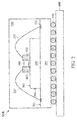
- FIG. 2 is a cross-sectional view of a semiconductor package assembly 500b in accordance with some embodiments of the disclosure.
- FIG. 4 is also a plan view of FIG. 2 , showing the arrangement of the semiconductor package assembly 500b.
- a molding compound and conductive wires of the semiconductor package assembly 500b are not shown in FIG. 4 .
- Elements of the embodiments hereinafter that are the same or similar as those previously described with reference to FIG. 1 are not repeated for brevity.
- the semiconductor die 300 of the semiconductor package assembly 500b may be coupled to the first substrate 300 through the flip chip technology.
- the pads (terminals) 402 of the passive device 400 are coupled to the corresponding pads 202 of the first substrate 200 through conductive wires 207.
- the semiconductor die 300 may comprise a flip-chip semiconductor die.
- the semiconductor die 300 is coupled to the first substrate 200 through the wire bonding technology.
- the semiconductor die 300 may be mounted on the top surface 201 of the first substrate 200 through an adhesion (not shown) between the semiconductor die 300 and the first substrate 200.
- the pads of the semiconductor die 300 are coupled to corresponding pads of the first substrate 200 through conductive wires.
- FIG. 3 is a cross-sectional view of a semiconductor package assembly 500c in accordance with some embodiments of the disclosure.
- FIG. 4 is also a plan view of FIG. 3 , showing the arrangement of the semiconductor package assembly 500c. For clearly showing the arrangement of a substrate, a semiconductor die and a passive device of the semiconductor package assembly 500c. A molding compound and conductive wires of the semiconductor package assembly 500c are not shown in FIG. 4 . Elements of the embodiments hereinafter that are the same or similar as those previously described with reference to FIG. 1-2 , are not repeated for brevity.
- the pads (terminals) 402 of the passive device 400 of the semiconductor package assembly 500c connect directly to the corresponding pads 304 of the semiconductor die 300.
- the pads 304 are disposed close to the top surface 301 of the semiconductor die 300.
- the semiconductor die 300 has a redistribution (redirect) function to provide for the passive device 400 mounted thereon.
- the pads (terminals) 402 of the passive device 400 may be redirected to other positions of the semiconductor die 300 (e.g. the positions of the pads 302) through the interconnection structure and the pads 302 and 304 of the semiconductor die 300.
- FIG. 5 is a cross-sectional view of a semiconductor package assembly 500d in accordance with some embodiments of the disclosure.
- FIG. 6 is a plan view of FIG. 5 , showing the arrangement of the semiconductor package assembly 500d.
- a first substrate, a semiconductor die, a second substrate and a passive device of the semiconductor package assembly 500d For clearly showing the arrangement of a first substrate, a semiconductor die, a second substrate and a passive device of the semiconductor package assembly 500d, a molding compound and conductive wires of the semiconductor package assembly 500d are not shown in FIG. 6 .
- Elements of the embodiments hereinafter that are the same or similar as those previously described with reference to FIG. 1-4 are not repeated for brevity.
- semiconductor package assembly 500d further comprises a carrier, such as second substrate 250, vertically between the semiconductor die 300 and the passive device 400.
- the discrete passive device 400 is separated from the semiconductor die 300 through the second substrate 250.
- the first substrate 200 and the second substrate 250 may have similar structures and may be formed by similar processes. It should be noted that the area of the second substrate 250 is less than that of the semiconductor die 300 and that of the first substrate 200 in a plan view, as shown in FIG. 6 . Therefore, the pads 302 of the semiconductor die 300 are exposed from the second substrate 250.
- the second substrate 250 includes pads 252 and 254 close to a top surface 251. Also, the second substrate 250 includes interconnection structures (not shown) coupled to the pads 252 and 254. In this embodiment, the second substrate 250 is designed to have the redistribution (redirect) function to provide for the passive device 400 mounted thereon.
- the passive device 400 is bonded on the second substrate 250, and the pads (terminals) 402 of the passive device 400 may be redirected to specific positions of the second substrate 250 (e.g. positions of the pads 208) through the routings (or the interconnection structure) and the pads 252 and 254 of the second substrate 250.
- the pads (terminals) 402 of the passive device 400 of the semiconductor package assembly 500d connect directly to the corresponding pads 254 of the second substrate 250.
- the pads 254 covered by the passive device 400 can be designed to be coupled to the pads 252, which are exposed from the passive device 400. Therefore, the passive device 400 can be coupled to the semiconductor die 300 through conductive wires 208.
- FIG. 7 is a cross-sectional view of a semiconductor package assembly 500e in accordance with some embodiments of the disclosure.
- FIG. 8 is a plan view of FIG. 7 , showing the arrangement of the semiconductor package assembly 500e.
- a molding compound and conductive wires of the semiconductor package assembly 500e are not shown in FIG. 8 .
- Elements of the embodiments hereinafter that are the same or similar as those previously described with reference to FIG. 1-6 are not repeated for brevity.
- semiconductor package assembly 500e further comprises one or more semiconductor dies, such as semiconductor dies 307 and 305, disposed directly on the second substrate 250.
- the passive device 400 is disposed beside the semiconductor dies 307 and 305. The pads 252 of the second substrate 250 are exposed from the passive device 400 and the semiconductor dies 307 and 305.
- the semiconductor dies 307 and 305 are coupled to the second substrate 250 through conductive structures. More specifically, pads 257 of the semiconductor die 307 are coupled to pads 255 of the second substrate 250 through conductive bumps 256. Some of pads 258 of the semiconductor die 305 are coupled to the corresponding pads 252 of the second substrate 250 through conductive wires 212. Also, some of the pads 258 of the semiconductor die 305 are coupled to the corresponding pads 302 of the semiconductor die 300 through conductive wires 214. Some other pads 258 of the semiconductor die 305 are coupled to the corresponding pads 202 of the first substrate 200 through conductive wires 216. In this embodiment, the semiconductor die 300 may comprise a flip-chip semiconductor die.
- the second substrate 250 is designed to have the redistribution (redirect) function to provide for the passive device 400, the semiconductor dies 307 and 305 mounted thereon.
- the pads (terminals) 402 of the passive device 400, the pads 257 of the semiconductor die 307 and the pads 258 of the semiconductor die 305 may be redirected to specific positions of the second substrate 250 (e.g. positions of the pads 252) through the routings (or the interconnection structure) and the pads 252 and 255 of the second substrate 250.
- the pads 252 of the second substrate 250 are exposed from the passive device 400, the semiconductor dies 307 and 305.
- the pads 252 of the second substrate 250 are coupled to the pads 302 of the semiconductor die 300 through conductive wires 208.
- the pads 252 of the second substrate 250 are coupled to the corresponding pads 202 of the first substrate 200 through conductive wires 210.
- FIG. 9 is a cross-sectional view of a semiconductor package assembly 500f in accordance with some embodiments of the disclosure.
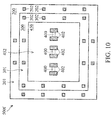
- FIG. 10 is a plan view of FIG. 9 , showing the arrangement of the semiconductor package assembly 500f.
- a molding compound and conductive wires of the semiconductor package assembly 500f are not shown in FIG. 10 .
- Elements of the embodiments hereinafter that are the same or similar as those previously described with reference to FIG. 1-8 are not repeated for brevity.
- semiconductor package assembly 500d further comprises a carrier; for example, an insulating material brick 450 located directly on the semiconductor die 300.
- the discrete passive devices 400 are embedded in the insulating material brick 450. Therefore, the passive devices 400 are separated from the semiconductor die 300 through the insulating material brick 450.
- the insulating material brick 450 may be mounted on the top surface 301 of the semiconductor die 300 through adhesion 453 between the insulating material brick 450 and the semiconductor die 300 and the first substrate 200.
- the semiconductor die 300 may comprise a flip-chip semiconductor die.
- the pads (terminals) 402 of the passive devices 400 are exposed from a surface 452 of the insulating material brick 450, which is located away from the semiconductor die 300.
- the insulating material brick 450 is formed of insulating materials.
- the insulating material brick 450 is free from any conductive structure coupled to the passive devices 400, so that the passive devices 400 are coupled to the semiconductor die 300 and/or the first substrate 200 only through external conductive structures, which are disposed outside of the insulating material brick 450.
- the pads (terminals) 402 of the passive devices 400 are coupled to the pads 302 of the semiconductor die 300 through conductive wires 260.
- the pads (terminals) 402 of the passive devices 400 are coupled to the corresponding pads 202 of the first substrate 200 through conductive wires 262.
- FIG. 11 is a cross-sectional view of a semiconductor package assembly 500g in accordance with some embodiments of the disclosure.
- FIG. 12 is a plan view of FIG. 11 , showing the arrangement of the semiconductor package assembly 500g. For clearly showing the arrangement of a first substrate, semiconductor dies, a second substrate, a passive device and a carrier of the semiconductor package assembly 500g. A molding compound and conductive wires of the semiconductor package assembly 500g are not shown in FIG. 12 . Elements of the embodiments hereinafter that are the same or similar as those previously described with reference to FIG. 1-10 , are not repeated for brevity.
- the semiconductor package assembly 500g further comprises a semiconductor die 306 embedded in the insulating material brick 450.
- the semiconductor die 306 is separated from the passive devices 400 through the insulating material brick 450.
- the pads (terminals) 402 of the passive devices 400 and pads 270 of the semiconductor die 306 are exposed from a surface 454 of the insulating material brick 450.
- the surface 454 is opposite from the surface 452 and close to the semiconductor die 300.
- the pads (terminals) 402 of the passive devices 400 and the pads 270 of the semiconductor die 306 are coupled to the pads 302 of the semiconductor die 300 through conductive bumps 264, which are disposed outside of the insulating material brick 450.
- the pads 302 of the semiconductor die 300 connecting to the conductive bumps 264 are covered by the insulating material brick 450.
- the passive devices 400 and the semiconductor die 306 are covered by the insulating material brick 450 in the plan view, as shown in FIG. 12 .
- the semiconductor die 300 may comprise a flip-chip semiconductor die.
- the semiconductor die 300 is coupled to the first substrate 200 through the wire bonding technology.
- the semiconductor die 300 may be mounted on the top surface 201 of the first substrate 200 through an adhesion (not shown) between the semiconductor die 300 and the first substrate 200. Also, the pads of the semiconductor die 300 are coupled to corresponding pads of the first substrate 200 through conductive wires.
- FIG. 13 is a cross-sectional view of a semiconductor package assembly 500h in accordance with some embodiments of the disclosure.
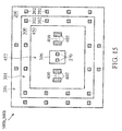
- FIG. 15 is a plan view of FIG. 13 , showing the arrangement of the semiconductor package assembly 500h.
- a molding compound and conductive wires of the semiconductor package assembly 500h are not shown in FIG. 15 .
- one of the differences between the semiconductor package assembly 500g shown in FIGS. 11-12 and the semiconductor package assembly 500h is that the pads (terminals) 402 of the passive devices 400 and the pads 270 of the semiconductor die 306 are exposed from the surface 452 of the insulating material brick 450, which is located away from the semiconductor die 300. Also, the surface of the semiconductor die 306 for the pads 270 to be disposed on is exposed from the surface 452 of the insulating material brick 450 in the plan view, as shown in FIG. 15 .
- the passive devices 400 and the semiconductor die 300 are coupled to the semiconductor die 300 and/or the first substrate 200 only through external conductive structures, which are disposed outside of the insulating material brick 450.
- the pads (terminals) 402 of the passive devices 400 and the pads 270 of the semiconductor die 306 are coupled to the pads 302 of the semiconductor die 300 through conductive wires 260 and 272.
- the pads (terminals) 402 of the passive devices 400 and the pads 270 of the semiconductor die 306 are coupled to the corresponding pads 202 of the first substrate 200 through conductive wires 262 and 274.
- the passive devices 400 of the semiconductor package assembly 500f, 500g or 500h may respectively be disposed close to the surfaces 452 and 454 of the same insulating material brick 450. Therefore, the pads (terminals) 402 of the different passive devices 400 may respectively be exposed from both the surfaces 452 and 454 of the insulating material brick 450.
- the semiconductor die 306 and the passive device 400 beside thereto may respectively be disposed close to the surfaces 452 and 454 of the same insulating material brick 450. Therefore, the pads 270 of the semiconductor die 306 and the pads (terminals) 402 of the passive device 400 may respectively be exposed from both the surfaces 452 and 454 of the insulating material brick 450.
- the passive devices 400 and the semiconductor die 306 embedded in the insulating material brick 450 may use the conductive bumps and conductive wires to electrically connect to the semiconductor die 300 and/or the first substrate 200.
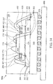
- FIG. 14 is a cross-sectional view of a semiconductor package assembly 500i in accordance with some embodiments of the disclosure.
- FIG. 15 is also a plan view of FIG. 14 , showing the arrangement of the semiconductor package assembly 500i.
- a molding compound and conductive wires of the semiconductor package assembly 500h are not shown in FIG. 15 .
- Elements of the embodiments hereinafter that are the same or similar as those previously described with reference to FIG. 1-13 are not repeated for brevity.
- the semiconductor die 306 of the semiconductor package assembly 500i is disposed directly on the insulating material brick 450. As shown in FIG. 13 , the semiconductor die 306 is disposed outside of the insulating material brick 450. More specifically, the semiconductor die 306 is disposed directly on the surface 452 of the insulating material brick 450, which is located away from the semiconductor die 300. In some embodiments, the semiconductor die 306 is disposed beside the passive devices 400 without covering the pads (terminals) 402 of the passive devices 400.
- the surface of the semiconductor die 306 for the pads 270 to be disposed on is exposed from the surface 452 of the insulating material brick 450 in the plan view, as shown in FIG. 15 . Also, the pads 270 of the semiconductor die 306 are not coplanar with the pads (terminals) 402 of the passive devices 400.
- Embodiments provide a semiconductor package assembly.
- the semiconductor package assembly includes a first substrate, a semiconductor die mounted on the first substrate, and a discrete passive device positioned directly on the semiconductor die.
- the discrete passive device can be coupled directly to the pads of the first semiconductor die.
- the passive device can be coupled to the semiconductor die through the conductive wires.
- the discrete passive device can be separated from the semiconductor die through a carrier therebetween.
- the area of the carrier is designed to be less than that of the semiconductor die and that of the first substrate.
- the carrier may comprise a second substrate or an insulating material brick. When the carrier includes the second substrate, the passive device may be disposed on the second substrate with the redistribution (redirect) function.
- the second substrate may provide for another semiconductor die mounted thereon.
- the terminals (pads) of the passive device may be redirected to other positions of the second substrate through the routings in the second substrate.
- the second substrate may provide for another semiconductor die embedded therein.
- the carrier includes the insulating material brick for the passive device to be embedded therein, the insulating material brick is free from any conductive structure coupled to the passive device.
- the pads of the passive device are exposed from the surface of the insulating material brick to couple to the semiconductor die and/or the first substrate only through external conductive structures.
- the insulating material brick may provide for another semiconductor die embedded therein or disposed thereon.
- the semiconductor package assembly may satisfy the requirements of being cost-efficient and having a small package size while maintaining the size of the passive device and the arrangement of the conductive bumps of the semiconductor package.
Landscapes
- Structures Or Materials For Encapsulating Or Coating Semiconductor Devices Or Solid State Devices (AREA)
- Semiconductor Integrated Circuits (AREA)
- Lead Frames For Integrated Circuits (AREA)
Applications Claiming Priority (3)
| Application Number | Priority Date | Filing Date | Title |
|---|---|---|---|
| US201562130048P | 2015-03-09 | 2015-03-09 | |
| US201562135322P | 2015-03-19 | 2015-03-19 | |
| US15/012,018 US9818727B2 (en) | 2015-03-09 | 2016-02-01 | Semiconductor package assembly with passive device |
Publications (3)
| Publication Number | Publication Date |
|---|---|
| EP3067928A2 true EP3067928A2 (de) | 2016-09-14 |
| EP3067928A3 EP3067928A3 (de) | 2016-11-30 |
| EP3067928B1 EP3067928B1 (de) | 2019-04-10 |
Family
ID=55359459
Family Applications (1)
| Application Number | Title | Priority Date | Filing Date |
|---|---|---|---|
| EP16155798.8A Active EP3067928B1 (de) | 2015-03-09 | 2016-02-16 | Halbleitergehäuseanordnung mit passiver vorrichtung |
Country Status (4)
| Country | Link |
|---|---|
| US (2) | US9818727B2 (de) |
| EP (1) | EP3067928B1 (de) |
| CN (1) | CN105957841B (de) |
| TW (1) | TWI642163B (de) |
Families Citing this family (6)
| Publication number | Priority date | Publication date | Assignee | Title |
|---|---|---|---|---|
| US9818727B2 (en) * | 2015-03-09 | 2017-11-14 | Mediatek Inc. | Semiconductor package assembly with passive device |
| WO2020118102A1 (en) | 2018-12-06 | 2020-06-11 | Analog Devices, Inc. | Shielded integrated device packages |
| EP3891793A4 (de) * | 2018-12-06 | 2022-10-05 | Analog Devices, Inc. | Integrierte vorrichtungspackungen mit passiven vorrichtungsanordnungen |
| CN111584478B (zh) * | 2020-05-22 | 2022-02-18 | 甬矽电子(宁波)股份有限公司 | 一种叠层芯片封装结构和叠层芯片封装方法 |
| TWI767770B (zh) * | 2021-06-25 | 2022-06-11 | 矽品精密工業股份有限公司 | 電子封裝件及其製法 |
| US12482795B2 (en) * | 2022-09-13 | 2025-11-25 | Nanya Technology Corporation | Semiconductor device with decoupling capacitor structure and method for manufacturing the same |
Family Cites Families (13)
| Publication number | Priority date | Publication date | Assignee | Title |
|---|---|---|---|---|
| US5905639A (en) | 1997-09-29 | 1999-05-18 | Raytheon Company | Three-dimensional component stacking using high density multichip interconnect decals and three-bond daisy-chained wedge bonds |
| US7176055B2 (en) | 2001-11-02 | 2007-02-13 | Matsushita Electric Industrial Co., Ltd. | Method and apparatus for manufacturing electronic component-mounted component, and electronic component-mounted component |
| CN100570844C (zh) | 2004-01-19 | 2009-12-16 | 上海集通数码科技有限责任公司 | 一种多芯片集成电路封装方法 |
| JP2006332094A (ja) | 2005-05-23 | 2006-12-07 | Seiko Epson Corp | 電子基板の製造方法及び半導体装置の製造方法並びに電子機器の製造方法 |
| US7539022B2 (en) * | 2005-10-04 | 2009-05-26 | Phoenix Precision Technology Corporation | Chip embedded packaging structure |
| DE102006016345A1 (de) | 2006-04-05 | 2007-10-18 | Infineon Technologies Ag | Halbleitermodul mit diskreten Bauelementen und Verfahren zur Herstellung desselben |
| JP2008034762A (ja) | 2006-07-31 | 2008-02-14 | Sanyo Electric Co Ltd | 回路装置 |
| US20090057867A1 (en) | 2007-08-30 | 2009-03-05 | Vincent Hool | Integrated Circuit Package with Passive Component |
| US7843047B2 (en) | 2008-11-21 | 2010-11-30 | Stats Chippac Ltd. | Encapsulant interposer system with integrated passive devices and manufacturing method therefor |
| US9530761B2 (en) * | 2011-09-02 | 2016-12-27 | Taiwan Semiconductor Manufacturing Company, Ltd. | Package systems including passive electrical components |
| US20130277855A1 (en) | 2012-04-24 | 2013-10-24 | Terry (Teckgyu) Kang | High density 3d package |
| CN203733790U (zh) | 2014-01-26 | 2014-07-23 | 深圳市兴森快捷电路科技股份有限公司 | 一种内部去耦的集成电路封装 |
| US9818727B2 (en) * | 2015-03-09 | 2017-11-14 | Mediatek Inc. | Semiconductor package assembly with passive device |
-
2016
- 2016-02-01 US US15/012,018 patent/US9818727B2/en active Active
- 2016-02-16 EP EP16155798.8A patent/EP3067928B1/de active Active
- 2016-02-25 TW TW105105598A patent/TWI642163B/zh not_active IP Right Cessation
- 2016-03-01 CN CN201610114652.7A patent/CN105957841B/zh active Active
-
2017
- 2017-10-06 US US15/726,471 patent/US10497678B2/en active Active
Non-Patent Citations (1)
| Title |
|---|
| None |
Also Published As
| Publication number | Publication date |
|---|---|
| US20160268233A1 (en) | 2016-09-15 |
| CN105957841B (zh) | 2019-02-01 |
| TWI642163B (zh) | 2018-11-21 |
| TW201705441A (zh) | 2017-02-01 |
| EP3067928A3 (de) | 2016-11-30 |
| US10497678B2 (en) | 2019-12-03 |
| EP3067928B1 (de) | 2019-04-10 |
| US20180033774A1 (en) | 2018-02-01 |
| CN105957841A (zh) | 2016-09-21 |
| US9818727B2 (en) | 2017-11-14 |
Similar Documents
| Publication | Publication Date | Title |
|---|---|---|
| US9978729B2 (en) | Semiconductor package assembly | |
| US10679949B2 (en) | Semiconductor package assembly with redistribution layer (RDL) trace | |
| US10497678B2 (en) | Semiconductor package assembly with passive device | |
| US10037938B2 (en) | Semiconductor packages | |
| CN107785277B (zh) | 电子封装结构及其制法 | |
| US9818683B2 (en) | Electronic package and method of fabricating the same | |
| US20130093103A1 (en) | Layered Semiconductor Package | |
| KR20080020069A (ko) | 반도체 패키지 및 그 제조방법 | |
| US9997498B2 (en) | Semiconductor package assembly | |
| US20090310322A1 (en) | Semiconductor Package | |
| JP2009506571A (ja) | インターポーザー基板に接続するための中間コンタクトを有するマイクロ電子デバイスおよびそれに関連する中間コンタクトを備えたマイクロ電子デバイスをパッケージする方法 | |
| US10147674B2 (en) | Semiconductor package assembly | |
| US20170294407A1 (en) | Passive element package and semiconductor module comprising the same | |
| CN112736043B (zh) | 多裸片封装模块及方法 | |
| US8723334B2 (en) | Semiconductor device including semiconductor package | |
| US10366906B2 (en) | Electronic package and its package substrate | |
| TWI447869B (zh) | 晶片堆疊封裝結構及其應用 | |
| US11239141B2 (en) | Lead frame package | |
| KR100325450B1 (ko) | 볼그리드어레이패키지 | |
| KR20080010993A (ko) | 적층 반도체 패키지 |
Legal Events
| Date | Code | Title | Description |
|---|---|---|---|
| PUAI | Public reference made under article 153(3) epc to a published international application that has entered the european phase |
Free format text: ORIGINAL CODE: 0009012 |
|
| AK | Designated contracting states |
Kind code of ref document: A2 Designated state(s): AL AT BE BG CH CY CZ DE DK EE ES FI FR GB GR HR HU IE IS IT LI LT LU LV MC MK MT NL NO PL PT RO RS SE SI SK SM TR |
|
| AX | Request for extension of the european patent |
Extension state: BA ME |
|
| PUAL | Search report despatched |
Free format text: ORIGINAL CODE: 0009013 |
|
| AK | Designated contracting states |
Kind code of ref document: A3 Designated state(s): AL AT BE BG CH CY CZ DE DK EE ES FI FR GB GR HR HU IE IS IT LI LT LU LV MC MK MT NL NO PL PT RO RS SE SI SK SM TR |
|
| AX | Request for extension of the european patent |
Extension state: BA ME |
|
| RIC1 | Information provided on ipc code assigned before grant |
Ipc: H01L 23/31 20060101ALN20161025BHEP Ipc: H01L 25/16 20060101AFI20161025BHEP Ipc: H01L 25/065 20060101ALN20161025BHEP |
|
| STAA | Information on the status of an ep patent application or granted ep patent |
Free format text: STATUS: REQUEST FOR EXAMINATION WAS MADE |
|
| STAA | Information on the status of an ep patent application or granted ep patent |
Free format text: STATUS: EXAMINATION IS IN PROGRESS |
|
| 17P | Request for examination filed |
Effective date: 20170510 |
|
| RBV | Designated contracting states (corrected) |
Designated state(s): AL AT BE BG CH CY CZ DE DK EE ES FI FR GB GR HR HU IE IS IT LI LT LU LV MC MK MT NL NO PL PT RO RS SE SI SK SM TR |
|
| 17Q | First examination report despatched |
Effective date: 20170620 |
|
| RIC1 | Information provided on ipc code assigned before grant |
Ipc: H01L 25/16 20060101AFI20180829BHEP Ipc: H01L 25/065 20060101ALN20180829BHEP Ipc: H01L 21/60 20060101ALI20180829BHEP Ipc: H01L 23/31 20060101ALN20180829BHEP |
|
| GRAP | Despatch of communication of intention to grant a patent |
Free format text: ORIGINAL CODE: EPIDOSNIGR1 |
|
| STAA | Information on the status of an ep patent application or granted ep patent |
Free format text: STATUS: GRANT OF PATENT IS INTENDED |
|
| RIC1 | Information provided on ipc code assigned before grant |
Ipc: H01L 23/31 20060101ALN20180919BHEP Ipc: H01L 25/16 20060101AFI20180919BHEP Ipc: H01L 21/60 20060101ALI20180919BHEP Ipc: H01L 25/065 20060101ALN20180919BHEP |
|
| INTG | Intention to grant announced |
Effective date: 20181015 |
|
| RIN1 | Information on inventor provided before grant (corrected) |
Inventor name: CHOU, CHE-YA Inventor name: CHEN, YING-CHIH Inventor name: KUO, CHE-HUNG |
|
| GRAS | Grant fee paid |
Free format text: ORIGINAL CODE: EPIDOSNIGR3 |
|
| GRAA | (expected) grant |
Free format text: ORIGINAL CODE: 0009210 |
|
| STAA | Information on the status of an ep patent application or granted ep patent |
Free format text: STATUS: THE PATENT HAS BEEN GRANTED |
|
| AK | Designated contracting states |
Kind code of ref document: B1 Designated state(s): AL AT BE BG CH CY CZ DE DK EE ES FI FR GB GR HR HU IE IS IT LI LT LU LV MC MK MT NL NO PL PT RO RS SE SI SK SM TR |
|
| REG | Reference to a national code |
Ref country code: GB Ref legal event code: FG4D |
|
| REG | Reference to a national code |
Ref country code: CH Ref legal event code: EP Ref country code: AT Ref legal event code: REF Ref document number: 1119840 Country of ref document: AT Kind code of ref document: T Effective date: 20190415 |
|
| REG | Reference to a national code |
Ref country code: IE Ref legal event code: FG4D |
|
| REG | Reference to a national code |
Ref country code: DE Ref legal event code: R096 Ref document number: 602016012062 Country of ref document: DE |
|
| REG | Reference to a national code |
Ref country code: NL Ref legal event code: MP Effective date: 20190410 |
|
| REG | Reference to a national code |
Ref country code: LT Ref legal event code: MG4D |
|
| REG | Reference to a national code |
Ref country code: AT Ref legal event code: MK05 Ref document number: 1119840 Country of ref document: AT Kind code of ref document: T Effective date: 20190410 |
|
| PG25 | Lapsed in a contracting state [announced via postgrant information from national office to epo] |
Ref country code: NL Free format text: LAPSE BECAUSE OF FAILURE TO SUBMIT A TRANSLATION OF THE DESCRIPTION OR TO PAY THE FEE WITHIN THE PRESCRIBED TIME-LIMIT Effective date: 20190410 |
|
| PG25 | Lapsed in a contracting state [announced via postgrant information from national office to epo] |
Ref country code: AL Free format text: LAPSE BECAUSE OF FAILURE TO SUBMIT A TRANSLATION OF THE DESCRIPTION OR TO PAY THE FEE WITHIN THE PRESCRIBED TIME-LIMIT Effective date: 20190410 Ref country code: ES Free format text: LAPSE BECAUSE OF FAILURE TO SUBMIT A TRANSLATION OF THE DESCRIPTION OR TO PAY THE FEE WITHIN THE PRESCRIBED TIME-LIMIT Effective date: 20190410 Ref country code: SE Free format text: LAPSE BECAUSE OF FAILURE TO SUBMIT A TRANSLATION OF THE DESCRIPTION OR TO PAY THE FEE WITHIN THE PRESCRIBED TIME-LIMIT Effective date: 20190410 Ref country code: HR Free format text: LAPSE BECAUSE OF FAILURE TO SUBMIT A TRANSLATION OF THE DESCRIPTION OR TO PAY THE FEE WITHIN THE PRESCRIBED TIME-LIMIT Effective date: 20190410 Ref country code: PT Free format text: LAPSE BECAUSE OF FAILURE TO SUBMIT A TRANSLATION OF THE DESCRIPTION OR TO PAY THE FEE WITHIN THE PRESCRIBED TIME-LIMIT Effective date: 20190910 Ref country code: NO Free format text: LAPSE BECAUSE OF FAILURE TO SUBMIT A TRANSLATION OF THE DESCRIPTION OR TO PAY THE FEE WITHIN THE PRESCRIBED TIME-LIMIT Effective date: 20190710 Ref country code: FI Free format text: LAPSE BECAUSE OF FAILURE TO SUBMIT A TRANSLATION OF THE DESCRIPTION OR TO PAY THE FEE WITHIN THE PRESCRIBED TIME-LIMIT Effective date: 20190410 Ref country code: LT Free format text: LAPSE BECAUSE OF FAILURE TO SUBMIT A TRANSLATION OF THE DESCRIPTION OR TO PAY THE FEE WITHIN THE PRESCRIBED TIME-LIMIT Effective date: 20190410 |
|
| PG25 | Lapsed in a contracting state [announced via postgrant information from national office to epo] |
Ref country code: LV Free format text: LAPSE BECAUSE OF FAILURE TO SUBMIT A TRANSLATION OF THE DESCRIPTION OR TO PAY THE FEE WITHIN THE PRESCRIBED TIME-LIMIT Effective date: 20190410 Ref country code: BG Free format text: LAPSE BECAUSE OF FAILURE TO SUBMIT A TRANSLATION OF THE DESCRIPTION OR TO PAY THE FEE WITHIN THE PRESCRIBED TIME-LIMIT Effective date: 20190710 Ref country code: RS Free format text: LAPSE BECAUSE OF FAILURE TO SUBMIT A TRANSLATION OF THE DESCRIPTION OR TO PAY THE FEE WITHIN THE PRESCRIBED TIME-LIMIT Effective date: 20190410 Ref country code: GR Free format text: LAPSE BECAUSE OF FAILURE TO SUBMIT A TRANSLATION OF THE DESCRIPTION OR TO PAY THE FEE WITHIN THE PRESCRIBED TIME-LIMIT Effective date: 20190711 Ref country code: PL Free format text: LAPSE BECAUSE OF FAILURE TO SUBMIT A TRANSLATION OF THE DESCRIPTION OR TO PAY THE FEE WITHIN THE PRESCRIBED TIME-LIMIT Effective date: 20190410 |
|
| PG25 | Lapsed in a contracting state [announced via postgrant information from national office to epo] |
Ref country code: IS Free format text: LAPSE BECAUSE OF FAILURE TO SUBMIT A TRANSLATION OF THE DESCRIPTION OR TO PAY THE FEE WITHIN THE PRESCRIBED TIME-LIMIT Effective date: 20190810 Ref country code: AT Free format text: LAPSE BECAUSE OF FAILURE TO SUBMIT A TRANSLATION OF THE DESCRIPTION OR TO PAY THE FEE WITHIN THE PRESCRIBED TIME-LIMIT Effective date: 20190410 |
|
| REG | Reference to a national code |
Ref country code: DE Ref legal event code: R097 Ref document number: 602016012062 Country of ref document: DE |
|
| PG25 | Lapsed in a contracting state [announced via postgrant information from national office to epo] |
Ref country code: DK Free format text: LAPSE BECAUSE OF FAILURE TO SUBMIT A TRANSLATION OF THE DESCRIPTION OR TO PAY THE FEE WITHIN THE PRESCRIBED TIME-LIMIT Effective date: 20190410 Ref country code: SK Free format text: LAPSE BECAUSE OF FAILURE TO SUBMIT A TRANSLATION OF THE DESCRIPTION OR TO PAY THE FEE WITHIN THE PRESCRIBED TIME-LIMIT Effective date: 20190410 Ref country code: EE Free format text: LAPSE BECAUSE OF FAILURE TO SUBMIT A TRANSLATION OF THE DESCRIPTION OR TO PAY THE FEE WITHIN THE PRESCRIBED TIME-LIMIT Effective date: 20190410 Ref country code: CZ Free format text: LAPSE BECAUSE OF FAILURE TO SUBMIT A TRANSLATION OF THE DESCRIPTION OR TO PAY THE FEE WITHIN THE PRESCRIBED TIME-LIMIT Effective date: 20190410 Ref country code: RO Free format text: LAPSE BECAUSE OF FAILURE TO SUBMIT A TRANSLATION OF THE DESCRIPTION OR TO PAY THE FEE WITHIN THE PRESCRIBED TIME-LIMIT Effective date: 20190410 |
|
| PLBE | No opposition filed within time limit |
Free format text: ORIGINAL CODE: 0009261 |
|
| STAA | Information on the status of an ep patent application or granted ep patent |
Free format text: STATUS: NO OPPOSITION FILED WITHIN TIME LIMIT |
|
| PG25 | Lapsed in a contracting state [announced via postgrant information from national office to epo] |
Ref country code: SM Free format text: LAPSE BECAUSE OF FAILURE TO SUBMIT A TRANSLATION OF THE DESCRIPTION OR TO PAY THE FEE WITHIN THE PRESCRIBED TIME-LIMIT Effective date: 20190410 Ref country code: IT Free format text: LAPSE BECAUSE OF FAILURE TO SUBMIT A TRANSLATION OF THE DESCRIPTION OR TO PAY THE FEE WITHIN THE PRESCRIBED TIME-LIMIT Effective date: 20190410 |
|
| 26N | No opposition filed |
Effective date: 20200113 |
|
| PG25 | Lapsed in a contracting state [announced via postgrant information from national office to epo] |
Ref country code: TR Free format text: LAPSE BECAUSE OF FAILURE TO SUBMIT A TRANSLATION OF THE DESCRIPTION OR TO PAY THE FEE WITHIN THE PRESCRIBED TIME-LIMIT Effective date: 20190410 |
|
| PG25 | Lapsed in a contracting state [announced via postgrant information from national office to epo] |
Ref country code: SI Free format text: LAPSE BECAUSE OF FAILURE TO SUBMIT A TRANSLATION OF THE DESCRIPTION OR TO PAY THE FEE WITHIN THE PRESCRIBED TIME-LIMIT Effective date: 20190410 |
|
| REG | Reference to a national code |
Ref country code: CH Ref legal event code: PL |
|
| REG | Reference to a national code |
Ref country code: BE Ref legal event code: MM Effective date: 20200229 |
|
| PG25 | Lapsed in a contracting state [announced via postgrant information from national office to epo] |
Ref country code: LU Free format text: LAPSE BECAUSE OF NON-PAYMENT OF DUE FEES Effective date: 20200216 Ref country code: MC Free format text: LAPSE BECAUSE OF FAILURE TO SUBMIT A TRANSLATION OF THE DESCRIPTION OR TO PAY THE FEE WITHIN THE PRESCRIBED TIME-LIMIT Effective date: 20190410 |
|
| PG25 | Lapsed in a contracting state [announced via postgrant information from national office to epo] |
Ref country code: CH Free format text: LAPSE BECAUSE OF NON-PAYMENT OF DUE FEES Effective date: 20200229 Ref country code: LI Free format text: LAPSE BECAUSE OF NON-PAYMENT OF DUE FEES Effective date: 20200229 |
|
| PG25 | Lapsed in a contracting state [announced via postgrant information from national office to epo] |
Ref country code: IE Free format text: LAPSE BECAUSE OF NON-PAYMENT OF DUE FEES Effective date: 20200216 |
|
| PG25 | Lapsed in a contracting state [announced via postgrant information from national office to epo] |
Ref country code: BE Free format text: LAPSE BECAUSE OF NON-PAYMENT OF DUE FEES Effective date: 20200229 |
|
| PG25 | Lapsed in a contracting state [announced via postgrant information from national office to epo] |
Ref country code: MT Free format text: LAPSE BECAUSE OF FAILURE TO SUBMIT A TRANSLATION OF THE DESCRIPTION OR TO PAY THE FEE WITHIN THE PRESCRIBED TIME-LIMIT Effective date: 20190410 Ref country code: CY Free format text: LAPSE BECAUSE OF FAILURE TO SUBMIT A TRANSLATION OF THE DESCRIPTION OR TO PAY THE FEE WITHIN THE PRESCRIBED TIME-LIMIT Effective date: 20190410 |
|
| PG25 | Lapsed in a contracting state [announced via postgrant information from national office to epo] |
Ref country code: MK Free format text: LAPSE BECAUSE OF FAILURE TO SUBMIT A TRANSLATION OF THE DESCRIPTION OR TO PAY THE FEE WITHIN THE PRESCRIBED TIME-LIMIT Effective date: 20190410 |
|
| P01 | Opt-out of the competence of the unified patent court (upc) registered |
Effective date: 20230607 |
|
| REG | Reference to a national code |
Ref country code: DE Ref legal event code: R079 Ref document number: 602016012062 Country of ref document: DE Free format text: PREVIOUS MAIN CLASS: H01L0025160000 Ipc: H10W0090000000 |
|
| PGFP | Annual fee paid to national office [announced via postgrant information from national office to epo] |
Ref country code: FR Payment date: 20251208 Year of fee payment: 11 |
|
| PGFP | Annual fee paid to national office [announced via postgrant information from national office to epo] |
Ref country code: GB Payment date: 20260106 Year of fee payment: 11 |
|
| PGFP | Annual fee paid to national office [announced via postgrant information from national office to epo] |
Ref country code: DE Payment date: 20251224 Year of fee payment: 11 |