EP3057126A1 - Power module, and method for producing same - Google Patents
Power module, and method for producing same Download PDFInfo
- Publication number
- EP3057126A1 EP3057126A1 EP14853126.2A EP14853126A EP3057126A1 EP 3057126 A1 EP3057126 A1 EP 3057126A1 EP 14853126 A EP14853126 A EP 14853126A EP 3057126 A1 EP3057126 A1 EP 3057126A1
- Authority
- EP
- European Patent Office
- Prior art keywords
- insulating layer
- power module
- metallic
- module according
- adhesive
- Prior art date
- Legal status (The legal status is an assumption and is not a legal conclusion. Google has not performed a legal analysis and makes no representation as to the accuracy of the status listed.)
- Granted
Links
Images






Classifications
-
- H—ELECTRICITY
- H10—SEMICONDUCTOR DEVICES; ELECTRIC SOLID-STATE DEVICES NOT OTHERWISE PROVIDED FOR
- H10W—GENERIC PACKAGES, INTERCONNECTIONS, CONNECTORS OR OTHER CONSTRUCTIONAL DETAILS OF DEVICES COVERED BY CLASS H10
- H10W70/00—Package substrates; Interposers; Redistribution layers [RDL]
- H10W70/20—Conductive package substrates serving as an interconnection, e.g. metal plates
- H10W70/24—Conductive package substrates serving as an interconnection, e.g. metal plates characterised by materials
-
- H—ELECTRICITY
- H10—SEMICONDUCTOR DEVICES; ELECTRIC SOLID-STATE DEVICES NOT OTHERWISE PROVIDED FOR
- H10W—GENERIC PACKAGES, INTERCONNECTIONS, CONNECTORS OR OTHER CONSTRUCTIONAL DETAILS OF DEVICES COVERED BY CLASS H10
- H10W40/00—Arrangements for thermal protection or thermal control
- H10W40/20—Arrangements for cooling
- H10W40/22—Arrangements for cooling characterised by their shape, e.g. having conical or cylindrical projections
-
- H—ELECTRICITY
- H10—SEMICONDUCTOR DEVICES; ELECTRIC SOLID-STATE DEVICES NOT OTHERWISE PROVIDED FOR
- H10W—GENERIC PACKAGES, INTERCONNECTIONS, CONNECTORS OR OTHER CONSTRUCTIONAL DETAILS OF DEVICES COVERED BY CLASS H10
- H10W40/00—Arrangements for thermal protection or thermal control
- H10W40/20—Arrangements for cooling
- H10W40/25—Arrangements for cooling characterised by their materials
- H10W40/251—Organics
-
- H—ELECTRICITY
- H10—SEMICONDUCTOR DEVICES; ELECTRIC SOLID-STATE DEVICES NOT OTHERWISE PROVIDED FOR
- H10W—GENERIC PACKAGES, INTERCONNECTIONS, CONNECTORS OR OTHER CONSTRUCTIONAL DETAILS OF DEVICES COVERED BY CLASS H10
- H10W40/00—Arrangements for thermal protection or thermal control
- H10W40/20—Arrangements for cooling
- H10W40/25—Arrangements for cooling characterised by their materials
- H10W40/255—Arrangements for cooling characterised by their materials having a laminate or multilayered structure, e.g. direct bond copper [DBC] ceramic substrates
-
- H—ELECTRICITY
- H10—SEMICONDUCTOR DEVICES; ELECTRIC SOLID-STATE DEVICES NOT OTHERWISE PROVIDED FOR
- H10W—GENERIC PACKAGES, INTERCONNECTIONS, CONNECTORS OR OTHER CONSTRUCTIONAL DETAILS OF DEVICES COVERED BY CLASS H10
- H10W40/00—Arrangements for thermal protection or thermal control
- H10W40/70—Fillings or auxiliary members in containers or in encapsulations for thermal protection or control
- H10W40/77—Auxiliary members characterised by their shape
- H10W40/778—Auxiliary members characterised by their shape in encapsulations
-
- H—ELECTRICITY
- H10—SEMICONDUCTOR DEVICES; ELECTRIC SOLID-STATE DEVICES NOT OTHERWISE PROVIDED FOR
- H10W—GENERIC PACKAGES, INTERCONNECTIONS, CONNECTORS OR OTHER CONSTRUCTIONAL DETAILS OF DEVICES COVERED BY CLASS H10
- H10W70/00—Package substrates; Interposers; Redistribution layers [RDL]
- H10W70/01—Manufacture or treatment
- H10W70/02—Manufacture or treatment of conductive package substrates serving as an interconnection, e.g. of metal plates
-
- H—ELECTRICITY
- H10—SEMICONDUCTOR DEVICES; ELECTRIC SOLID-STATE DEVICES NOT OTHERWISE PROVIDED FOR
- H10W—GENERIC PACKAGES, INTERCONNECTIONS, CONNECTORS OR OTHER CONSTRUCTIONAL DETAILS OF DEVICES COVERED BY CLASS H10
- H10W70/00—Package substrates; Interposers; Redistribution layers [RDL]
- H10W70/40—Leadframes
- H10W70/411—Chip-supporting parts, e.g. die pads
- H10W70/413—Insulating or insulated substrates serving as die pads
-
- H—ELECTRICITY
- H10—SEMICONDUCTOR DEVICES; ELECTRIC SOLID-STATE DEVICES NOT OTHERWISE PROVIDED FOR
- H10W—GENERIC PACKAGES, INTERCONNECTIONS, CONNECTORS OR OTHER CONSTRUCTIONAL DETAILS OF DEVICES COVERED BY CLASS H10
- H10W70/00—Package substrates; Interposers; Redistribution layers [RDL]
- H10W70/40—Leadframes
- H10W70/421—Shapes or dispositions
-
- H—ELECTRICITY
- H10—SEMICONDUCTOR DEVICES; ELECTRIC SOLID-STATE DEVICES NOT OTHERWISE PROVIDED FOR
- H10W—GENERIC PACKAGES, INTERCONNECTIONS, CONNECTORS OR OTHER CONSTRUCTIONAL DETAILS OF DEVICES COVERED BY CLASS H10
- H10W70/00—Package substrates; Interposers; Redistribution layers [RDL]
- H10W70/40—Leadframes
- H10W70/421—Shapes or dispositions
- H10W70/442—Shapes or dispositions of multiple leadframes in a single chip
-
- H—ELECTRICITY
- H10—SEMICONDUCTOR DEVICES; ELECTRIC SOLID-STATE DEVICES NOT OTHERWISE PROVIDED FOR
- H10W—GENERIC PACKAGES, INTERCONNECTIONS, CONNECTORS OR OTHER CONSTRUCTIONAL DETAILS OF DEVICES COVERED BY CLASS H10
- H10W70/00—Package substrates; Interposers; Redistribution layers [RDL]
- H10W70/40—Leadframes
- H10W70/464—Additional interconnections in combination with leadframes
- H10W70/468—Circuit boards
-
- H—ELECTRICITY
- H10—SEMICONDUCTOR DEVICES; ELECTRIC SOLID-STATE DEVICES NOT OTHERWISE PROVIDED FOR
- H10W—GENERIC PACKAGES, INTERCONNECTIONS, CONNECTORS OR OTHER CONSTRUCTIONAL DETAILS OF DEVICES COVERED BY CLASS H10
- H10W72/00—Interconnections or connectors in packages
- H10W72/071—Connecting or disconnecting
- H10W72/075—Connecting or disconnecting of bond wires
-
- H—ELECTRICITY
- H10—SEMICONDUCTOR DEVICES; ELECTRIC SOLID-STATE DEVICES NOT OTHERWISE PROVIDED FOR
- H10W—GENERIC PACKAGES, INTERCONNECTIONS, CONNECTORS OR OTHER CONSTRUCTIONAL DETAILS OF DEVICES COVERED BY CLASS H10
- H10W74/00—Encapsulations, e.g. protective coatings
- H10W74/01—Manufacture or treatment
- H10W74/016—Manufacture or treatment using moulds
-
- H—ELECTRICITY
- H10—SEMICONDUCTOR DEVICES; ELECTRIC SOLID-STATE DEVICES NOT OTHERWISE PROVIDED FOR
- H10W—GENERIC PACKAGES, INTERCONNECTIONS, CONNECTORS OR OTHER CONSTRUCTIONAL DETAILS OF DEVICES COVERED BY CLASS H10
- H10W74/00—Encapsulations, e.g. protective coatings
- H10W74/10—Encapsulations, e.g. protective coatings characterised by their shape or disposition
- H10W74/111—Encapsulations, e.g. protective coatings characterised by their shape or disposition the semiconductor body being completely enclosed
- H10W74/114—Encapsulations, e.g. protective coatings characterised by their shape or disposition the semiconductor body being completely enclosed by a substrate and the encapsulations
-
- H—ELECTRICITY
- H10—SEMICONDUCTOR DEVICES; ELECTRIC SOLID-STATE DEVICES NOT OTHERWISE PROVIDED FOR
- H10W—GENERIC PACKAGES, INTERCONNECTIONS, CONNECTORS OR OTHER CONSTRUCTIONAL DETAILS OF DEVICES COVERED BY CLASS H10
- H10W90/00—Package configurations
-
- H—ELECTRICITY
- H10—SEMICONDUCTOR DEVICES; ELECTRIC SOLID-STATE DEVICES NOT OTHERWISE PROVIDED FOR
- H10W—GENERIC PACKAGES, INTERCONNECTIONS, CONNECTORS OR OTHER CONSTRUCTIONAL DETAILS OF DEVICES COVERED BY CLASS H10
- H10W90/00—Package configurations
- H10W90/811—Multiple chips on leadframes
-
- H—ELECTRICITY
- H10—SEMICONDUCTOR DEVICES; ELECTRIC SOLID-STATE DEVICES NOT OTHERWISE PROVIDED FOR
- H10W—GENERIC PACKAGES, INTERCONNECTIONS, CONNECTORS OR OTHER CONSTRUCTIONAL DETAILS OF DEVICES COVERED BY CLASS H10
- H10W72/00—Interconnections or connectors in packages
- H10W72/071—Connecting or disconnecting
- H10W72/073—Connecting or disconnecting of die-attach connectors
-
- H—ELECTRICITY
- H10—SEMICONDUCTOR DEVICES; ELECTRIC SOLID-STATE DEVICES NOT OTHERWISE PROVIDED FOR
- H10W—GENERIC PACKAGES, INTERCONNECTIONS, CONNECTORS OR OTHER CONSTRUCTIONAL DETAILS OF DEVICES COVERED BY CLASS H10
- H10W72/00—Interconnections or connectors in packages
- H10W72/071—Connecting or disconnecting
- H10W72/073—Connecting or disconnecting of die-attach connectors
- H10W72/07331—Connecting techniques
- H10W72/07336—Soldering or alloying
-
- H—ELECTRICITY
- H10—SEMICONDUCTOR DEVICES; ELECTRIC SOLID-STATE DEVICES NOT OTHERWISE PROVIDED FOR
- H10W—GENERIC PACKAGES, INTERCONNECTIONS, CONNECTORS OR OTHER CONSTRUCTIONAL DETAILS OF DEVICES COVERED BY CLASS H10
- H10W72/00—Interconnections or connectors in packages
- H10W72/30—Die-attach connectors
- H10W72/321—Structures or relative sizes of die-attach connectors
- H10W72/325—Die-attach connectors having a filler embedded in a matrix
-
- H—ELECTRICITY
- H10—SEMICONDUCTOR DEVICES; ELECTRIC SOLID-STATE DEVICES NOT OTHERWISE PROVIDED FOR
- H10W—GENERIC PACKAGES, INTERCONNECTIONS, CONNECTORS OR OTHER CONSTRUCTIONAL DETAILS OF DEVICES COVERED BY CLASS H10
- H10W72/00—Interconnections or connectors in packages
- H10W72/30—Die-attach connectors
- H10W72/351—Materials of die-attach connectors
- H10W72/353—Materials of die-attach connectors not comprising solid metals or solid metalloids, e.g. ceramics
-
- H—ELECTRICITY
- H10—SEMICONDUCTOR DEVICES; ELECTRIC SOLID-STATE DEVICES NOT OTHERWISE PROVIDED FOR
- H10W—GENERIC PACKAGES, INTERCONNECTIONS, CONNECTORS OR OTHER CONSTRUCTIONAL DETAILS OF DEVICES COVERED BY CLASS H10
- H10W72/00—Interconnections or connectors in packages
- H10W72/50—Bond wires
- H10W72/531—Shapes of wire connectors
- H10W72/5363—Shapes of wire connectors the connected ends being wedge-shaped
-
- H—ELECTRICITY
- H10—SEMICONDUCTOR DEVICES; ELECTRIC SOLID-STATE DEVICES NOT OTHERWISE PROVIDED FOR
- H10W—GENERIC PACKAGES, INTERCONNECTIONS, CONNECTORS OR OTHER CONSTRUCTIONAL DETAILS OF DEVICES COVERED BY CLASS H10
- H10W72/00—Interconnections or connectors in packages
- H10W72/50—Bond wires
- H10W72/541—Dispositions of bond wires
- H10W72/5445—Dispositions of bond wires being orthogonal to a side surface of the chip, e.g. parallel arrangements
-
- H—ELECTRICITY
- H10—SEMICONDUCTOR DEVICES; ELECTRIC SOLID-STATE DEVICES NOT OTHERWISE PROVIDED FOR
- H10W—GENERIC PACKAGES, INTERCONNECTIONS, CONNECTORS OR OTHER CONSTRUCTIONAL DETAILS OF DEVICES COVERED BY CLASS H10
- H10W72/00—Interconnections or connectors in packages
- H10W72/50—Bond wires
- H10W72/541—Dispositions of bond wires
- H10W72/547—Dispositions of multiple bond wires
- H10W72/5473—Dispositions of multiple bond wires multiple bond wires connected to a common bond pad
-
- H—ELECTRICITY
- H10—SEMICONDUCTOR DEVICES; ELECTRIC SOLID-STATE DEVICES NOT OTHERWISE PROVIDED FOR
- H10W—GENERIC PACKAGES, INTERCONNECTIONS, CONNECTORS OR OTHER CONSTRUCTIONAL DETAILS OF DEVICES COVERED BY CLASS H10
- H10W72/00—Interconnections or connectors in packages
- H10W72/50—Bond wires
- H10W72/541—Dispositions of bond wires
- H10W72/547—Dispositions of multiple bond wires
- H10W72/5475—Dispositions of multiple bond wires multiple bond wires connected to common bond pads at both ends of the wires
-
- H—ELECTRICITY
- H10—SEMICONDUCTOR DEVICES; ELECTRIC SOLID-STATE DEVICES NOT OTHERWISE PROVIDED FOR
- H10W—GENERIC PACKAGES, INTERCONNECTIONS, CONNECTORS OR OTHER CONSTRUCTIONAL DETAILS OF DEVICES COVERED BY CLASS H10
- H10W72/00—Interconnections or connectors in packages
- H10W72/50—Bond wires
- H10W72/551—Materials of bond wires
- H10W72/552—Materials of bond wires comprising metals or metalloids, e.g. silver
- H10W72/5524—Materials of bond wires comprising metals or metalloids, e.g. silver comprising aluminium [Al]
-
- H—ELECTRICITY
- H10—SEMICONDUCTOR DEVICES; ELECTRIC SOLID-STATE DEVICES NOT OTHERWISE PROVIDED FOR
- H10W—GENERIC PACKAGES, INTERCONNECTIONS, CONNECTORS OR OTHER CONSTRUCTIONAL DETAILS OF DEVICES COVERED BY CLASS H10
- H10W72/00—Interconnections or connectors in packages
- H10W72/851—Dispositions of multiple connectors or interconnections
- H10W72/874—On different surfaces
- H10W72/884—Die-attach connectors and bond wires
-
- H—ELECTRICITY
- H10—SEMICONDUCTOR DEVICES; ELECTRIC SOLID-STATE DEVICES NOT OTHERWISE PROVIDED FOR
- H10W—GENERIC PACKAGES, INTERCONNECTIONS, CONNECTORS OR OTHER CONSTRUCTIONAL DETAILS OF DEVICES COVERED BY CLASS H10
- H10W72/00—Interconnections or connectors in packages
- H10W72/90—Bond pads, in general
- H10W72/921—Structures or relative sizes of bond pads
- H10W72/926—Multiple bond pads having different sizes
-
- H—ELECTRICITY
- H10—SEMICONDUCTOR DEVICES; ELECTRIC SOLID-STATE DEVICES NOT OTHERWISE PROVIDED FOR
- H10W—GENERIC PACKAGES, INTERCONNECTIONS, CONNECTORS OR OTHER CONSTRUCTIONAL DETAILS OF DEVICES COVERED BY CLASS H10
- H10W72/00—Interconnections or connectors in packages
- H10W72/90—Bond pads, in general
- H10W72/931—Shapes of bond pads
- H10W72/932—Plan-view shape, i.e. in top view
-
- H—ELECTRICITY
- H10—SEMICONDUCTOR DEVICES; ELECTRIC SOLID-STATE DEVICES NOT OTHERWISE PROVIDED FOR
- H10W—GENERIC PACKAGES, INTERCONNECTIONS, CONNECTORS OR OTHER CONSTRUCTIONAL DETAILS OF DEVICES COVERED BY CLASS H10
- H10W74/00—Encapsulations, e.g. protective coatings
-
- H—ELECTRICITY
- H10—SEMICONDUCTOR DEVICES; ELECTRIC SOLID-STATE DEVICES NOT OTHERWISE PROVIDED FOR
- H10W—GENERIC PACKAGES, INTERCONNECTIONS, CONNECTORS OR OTHER CONSTRUCTIONAL DETAILS OF DEVICES COVERED BY CLASS H10
- H10W90/00—Package configurations
- H10W90/701—Package configurations characterised by the relative positions of pads or connectors relative to package parts
- H10W90/731—Package configurations characterised by the relative positions of pads or connectors relative to package parts of die-attach connectors
- H10W90/736—Package configurations characterised by the relative positions of pads or connectors relative to package parts of die-attach connectors between a chip and a stacked lead frame, conducting package substrate or heat sink
-
- H—ELECTRICITY
- H10—SEMICONDUCTOR DEVICES; ELECTRIC SOLID-STATE DEVICES NOT OTHERWISE PROVIDED FOR
- H10W—GENERIC PACKAGES, INTERCONNECTIONS, CONNECTORS OR OTHER CONSTRUCTIONAL DETAILS OF DEVICES COVERED BY CLASS H10
- H10W90/00—Package configurations
- H10W90/701—Package configurations characterised by the relative positions of pads or connectors relative to package parts
- H10W90/751—Package configurations characterised by the relative positions of pads or connectors relative to package parts of bond wires
- H10W90/753—Package configurations characterised by the relative positions of pads or connectors relative to package parts of bond wires between laterally-adjacent chips
-
- H—ELECTRICITY
- H10—SEMICONDUCTOR DEVICES; ELECTRIC SOLID-STATE DEVICES NOT OTHERWISE PROVIDED FOR
- H10W—GENERIC PACKAGES, INTERCONNECTIONS, CONNECTORS OR OTHER CONSTRUCTIONAL DETAILS OF DEVICES COVERED BY CLASS H10
- H10W90/00—Package configurations
- H10W90/701—Package configurations characterised by the relative positions of pads or connectors relative to package parts
- H10W90/751—Package configurations characterised by the relative positions of pads or connectors relative to package parts of bond wires
- H10W90/754—Package configurations characterised by the relative positions of pads or connectors relative to package parts of bond wires between a chip and a stacked insulating package substrate, interposer or RDL
-
- H—ELECTRICITY
- H10—SEMICONDUCTOR DEVICES; ELECTRIC SOLID-STATE DEVICES NOT OTHERWISE PROVIDED FOR
- H10W—GENERIC PACKAGES, INTERCONNECTIONS, CONNECTORS OR OTHER CONSTRUCTIONAL DETAILS OF DEVICES COVERED BY CLASS H10
- H10W90/00—Package configurations
- H10W90/701—Package configurations characterised by the relative positions of pads or connectors relative to package parts
- H10W90/751—Package configurations characterised by the relative positions of pads or connectors relative to package parts of bond wires
- H10W90/756—Package configurations characterised by the relative positions of pads or connectors relative to package parts of bond wires between a chip and a stacked lead frame, conducting package substrate or heat sink
Definitions
- the present invention described herein relates to a power module and a fabrication method for such a power module.
- the present invention relates to a power module having reduced cost, stabilized quality, and improved reliability; and a fabrication method for such a power module.
- the object of the present invention is to provide: a power module having reduced cost, reduced warpage of the whole of a substrate, stabilized quality, and improved reliability; and a fabrication method for such a power module.
- a power module comprising: an insulating layer; a metallic plate disposed on the insulating layer; a semiconductor device disposed on the metallic plate; a first adhesive insulating layer and a second adhesive insulating layer respectively disposed on the metallic plate; a metallic land for main electrode wiring disposed on the first adhesive insulating layer; and a metallic land for signal wiring disposed on the second adhesive insulating layer.
- a fabrication method for a power module comprising: forming a metallic plate; forming a semiconductor device via a solder on a surface of the metallic plate; forming a first adhesive insulating layer and a second adhesive insulating layer on the metallic plate; forming a metallic land for main electrode wiring on the first adhesive insulating layer, and forming a metallic land for signal wiring on the second adhesive insulating layer; bonding-connecting between the semiconductor device and the metallic land for main electrode wiring via a first bonding wire; bonding-connecting between the semiconductor device and the metallic land for signal wiring via a second bonding wire; molding the metallic plate, the first adhesive insulating layer, the second adhesive insulating layer, the metallic land for main electrode wiring, the metallic land for signal wiring, the semiconductor device, the first bonding wire, and the second bonding wire using a mold resin; and forming an insulating layer on a back side surface of the metallic plate.
- a power module having reduced cost, reduced warpage of the whole of a substrate, stabilized quality, and improved reliability; and a fabrication method for such a power module.
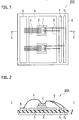
- Fig. 1 shows a schematic planar pattern configuration of a 1-in-1 module, which is a power module semiconductor device 2a according to a comparative example.
- Fig. 2 shows a schematic cross-sectional structure taken in the line I-I of Fig. 1 .
- a semiconductor chip 1 is connected to a collector connecting electrode 3 via solder 2 under the chip, as shown in Figs. 1 and 2 .
- a bonding wire 4 for emitter is connected to between an emitter electrode of the semiconductor chip 1 and a metallic land 5 for emitter wiring for the purpose of extraction of a current from an emitter of the semiconductor chip 1.
- wiring (not shown) for extracting the current from the metallic land 5 for emitter wiring to the outside is constructed to the metallic land 5 for emitter wiring.
- a bonding wire 6 1 for gate signal is connected to between a gate electrode of the semiconductor chip 1 and the metallic land 7 1 for signal wiring
- a bonding wire 6 2 for emitter signal is connected to between the emitter electrode of the semiconductor chip 1 and metallic land 7 2 for emitter signal wiring.
- the collector connecting electrode 3, the metallic land 5 for emitter wiring, the metallic lands 7 1 , 7 2 for signal wiring, and a back surface copper foil 9 are respectively bonded to a ceramics substrate 8.
- a ceramics substrate 8 Such a structure can be formed by process insulating substrates, e.g. commercially available Direct Bonding Copper (DBC), for example.
- DBC Direct Bonding Copper
- the power module 20A according to the comparative example requires a high cost since it is necessary to request fabrication of the insulating substrate to insulating substrate manufacturers. Moreover, if various circuit patterns are required, a substrate template for every circuit pattern is required, thereby taking a high cost. Moreover, warpage may occur in the insulating substrate due to a coefficient thermal expansion (CTE) difference between the ceramics substrate and the copper circuit pattern.
- CTE coefficient thermal expansion
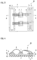
- Fig. 3 is a schematic planar pattern configuration of IGBT of a 1-in-1 module, which is a power module 20 according to an embodiment.
- Fig. 4 shows a schematic cross-sectional structure taken in the line II-II of Fig. 3 .
- the power module 20 includes: an insulating layer 12; a metallic plate 3 disposed on the insulating layer 12; a semiconductor device 1 disposed on the metallic plate 3; a first adhesive insulating layer 10 and a second adhesive insulating layer 11 respectively disposed on the metallic plate 3; a metallic land 5 for main electrode wiring disposed on the first adhesive insulating layer 10; and metallic lands 7 1 , 7 2 for signal wiring disposed on the second adhesive insulating layer 11.
- the metallic land 5 for main electrode wiring and the metallic lands 7 1 , 7 2 for signal wiring are formed on the metallic plate 3 having a wiring pattern on which the semiconductor device 1 is mounted via the first and second adhesive insulating layers (10, 11).
- the metallic lands 5, 7 1 and 7 2 have wiring patterns other than the wiring pattern on the metallic plate 3.
- the first adhesive insulating layer 10 and the second adhesive insulating layer 11 are formed with an inorganic adhesive agent, in the power module 20 according to the embodiment.
- the inorganic adhesive agent contains a filler
- the filler may be one selected from the group consisting of silica, alumina, zirconia, and a complex thereof, for example.
- the metallic plate 3 can be formed of one selected from the group consist of copper, aluminum (aluminium), a copper alloy and an aluminum alloy (aluminium alloy).
- the power module 20 includes: a first bonding wire 4 configured to electrically connect between the semiconductor device 1 and the metallic land 5 for main electrode wiring; a second bonding wire 6 configured to electrically connect between the semiconductor device 1 and the metallic lands 7 1 , 7 2 for signal wiring; and a mold resin (17: refer to Figs. 11 and 12 ) for molding the metallic plate, the first and second adhesive insulating layers, the metallic land for main electrode wiring, the metallic land for signal wiring, the semiconductor device, and the first and second bonding wires.
- Fig. 5 is a schematic planar pattern configuration of IGBT of a 1-in-1 module, which is a power module 20 according to a modified example of the embodiment.
- Fig. 6 shows a schematic cross-sectional structure taken in the line III-III of Fig. 5 .
- each of the first adhesive insulating layer 10A and the second adhesive insulating layer 11A is formed of a heat-resistant insulating sheet, in the power module 20 according to the modified example of the embodiment.
- the heat-resistant insulating sheet may be formed of one selected from the group consist of an epoxy based resin and a polyimide based resin, for example.
- the thickness of the heat-resistant insulating sheet is approximately 30 ⁇ m to approximately 120 ⁇ m, for example, and therefore the heat-resistant insulating sheet is relatively thin as one layer. Accordingly, the heat-resistant insulating sheet may be formed of a multilayered sheet.
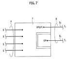
- Fig. 7 shows an enlarged schematic planar pattern configuration of a surface portion of a semiconductor device 1 applied to the power modules 20 according to the embodiment and its modified example.
- a source pad electrode SP or an emitter pad electrode EP, and a gate pad electrode GP are disposed on the surface of the semiconductor device 1.
- the first bonding wire 4 electrically connected to the metallic land 5 for main electrode wiring and the second bonding wire 6 2 connected to the metallic land 7 2 for signal wiring are connected onto the source pad electrode SP or emitter pad electrode EP.
- the first bonding wire 6 1 connected to the metallic land 7 1 for signal wiring is connected onto the gate pad electrode GP.
- the emitter pad electrode EP is formed on the surface of the semiconductor device 1 if the semiconductor device 1 is IGBT, but the source pad electrode SP is formed on the surface of the semiconductor device 1 if the semiconductor device 1 is SiC MOSFET.
- Fig. 8(a) shows a cross-sectional structure showing a state where the semiconductor device 1 is bonded via solder 2 under the chip on the metallic plate (collector connecting electrode) 3, in a process chart showing a fabrication method of the power module 20 according to the embodiment.
- Fig. 8(b) shows a cross-sectional structure showing a state after disposing the adhesive insulating layer 10 for emitter and the adhesive insulating layer 11 for signal wiring on the collector connecting electrode 3.
- Fig. 8(b) shows a cross-sectional structure showing a state after disposing the adhesive insulating layer 10 for emitter and the adhesive insulating layer 11 for signal wiring on the collector connecting electrode 3.
- Fig. 8(b) shows a cross-sectional structure showing a state after disposing the adhesive insulating layer 10 for emitter and the adhesive insulating layer 11 for signal wiring on the collector connecting electrode 3.
- Fig. 8(b) shows a cross-sectional structure showing a state after disposing the adhesive insulating layer 10 for emitter and the
- FIG. 8(c) shows a cross-sectional structure showing a state where the metallic land 5 for emitter wiring is mounted on the adhesive insulating layer 10 for emitter and the metallic lands 7 1 , 7 2 for signal wiring are mounted on the adhesive insulating layer 11 for signal wiring, and then a heating and pressurizing process is performed.
- Fig. 8(d) shows a cross-sectional structure showing a state where the semiconductor device 1 and the metallic land 5 for emitter wiring are bonding-connected via the bonding wire 4 for emitter, and the semiconductor device 1 and the metallic lands 7 1 , 7 2 for signal wiring are respectively bonding-connected via the bonding wires 6 (6 1 , 6 2 ) for signal.
- Fig. 9 shows a schematic planar pattern configuration in a state where the metallic land 5 for emitter wiring is mounted on the adhesive insulating layer 10 for emitter, and the metallic lands 7 1 , 7 2 for signal wiring are mounted on the adhesive insulating layer 11 for signal wiring.
- Fig. 10 shows a schematic cross-sectional structure taken in the line IV-IV of Fig. 9 , in a state where the metallic land 5 for emitter wiring is bonded onto the adhesive insulating layer 10 for emitter, and the metallic lands 7 1 , 7 2 for signal wiring are bonded onto the adhesive insulating layer 11 for signal wiring, with a heating and pressurizing process.
- a hot plate 120 is applicable as a heating method.
- a thermostatic oven, a hot air dryer, etc. may also be used therefor. Heating processing temperature is approximately 100 degrees C to approximately 200 degrees C, for example.
- Pressurizing pressure P is approximately 20 kg/cm 2 , for example.
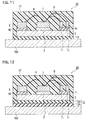
- Fig. 11 shows a cross-sectional structure showing a state where a relatively-hard insulating layer 12a and a relatively-soft insulating layer 12b already formed on the back side surface of the collector connecting electrode 3 already subjected to molding using a mold resin 17 are disposed on the heat sink 100, after the bonding process shown in Fig. 8(d) .
- Fig. 12 shows a cross-sectional structure showing a state where a relatively-hard insulating layer 12a and a relatively-soft insulating layer 12b already formed on the back side surface of the collector connecting electrode 3 already subjected to molding using a mold resin 17 are disposed on the heat sink 100, after the bonding process shown in Fig. 8(d) .
- the fabrication method of the power module 20 includes: forming a metallic plate 3; forming a semiconductor device 1 via solder 2 under the chip on the surface of the metallic plate 3; forming a first adhesive insulating layer 10 and a second adhesive insulating layer 11 on the metallic plate 3; forming a metallic land 5 for main electrode wiring on the first adhesive insulating layer 10, and forming metallic lands 7 1 , 7 2 for signal wiring on the second adhesive insulating layer 11; bonding-connecting between the semiconductor device 1 and the metallic land 5 for main electrode wiring via a first bonding wire 4; bonding-connecting between the semiconductor device 1 and the metallic lands 7 1 , 7 2 for signal wiring via bonding wires 6 (6 1 , 6 2 ); molding the metallic plate 3, the first adhesive insulating layer 10, the second adhesive insulating layer 11, the metallic land 5 for main electrode wiring, the metallic lands 7 1 , 7 2 for signal wiring, the semiconductor device 1, the first adhesive insulating layer 10 and a second adhesive insulating layer 11 on the metallic plate 3; forming
- the step of forming the insulating layer 12 on the back side surface of the metallic plate 3 may include: forming a relatively-hard insulating layer 12a on the back side surface of the metallic plate 3; and forming a relatively-soft insulating layer 12b on the relatively-hard insulating layer 12a.
- the step of forming the metallic land 5 for main electrode wiring on the first adhesive insulating layer 10 and forming the metallic lands 7 1 , 7 2 for signal wiring on the second adhesive insulating layer 11 includes a heating and pressurizing process.
- first adhesive insulating layer 10 and the second adhesive insulating layer 11 can be formed of an inorganic adhesive agent.
- the inorganic adhesive agent contains a filler
- the filler may be silica, alumina, zirconia, or a complex thereof, for example.
- the power module 20 according to the embodiment as shown in Figs. 11 and 12 is completed through the above-mentioned fabricating process.
- the power module 20 there is no need of fabricating a substrate template for newly fabricating the insulating substrate even if the number of the semiconductor devices 1 to be mounted or disposition of the semiconductor devices is changed, since a shape of the metallic land 5 for emitter wiring or the metallic lands 7 1 , 7 2 for signal wiring can be appropriately changed in accordance therewith, and then can be fixed to the metallic plate (collector connecting electrode) 3 using the inorganic adhesive agent.
- the insulating layer 12 may be formed of an organic insulating resin layer.
- the power module 20 may include a cooling plate (heat sink) 100 as shown in Figs. 11 and 12 , and the insulating layer 12 may be disposed at the cooling plate side.
- a cooling plate heat sink 100 as shown in Figs. 11 and 12
- the insulating layer 12 may be disposed at the cooling plate side.
- the insulating layer 12 includes: a relatively-hard insulating layer 12a disposed at a metallic plate 3 side; and a relatively-soft insulating layer 12b disposed at a side opposite to the metallic plate 3 side.
- the power module 20 may include a cooling plate (heat sink) 100, and the relatively-soft insulating layer 12b may be disposed at the cooling plate (heat sink) 100 side.
- the relatively-soft insulating layer 12b may be formed of an organic material(s).
- the relatively-soft insulating layer 12b may be formed of a silicone based resin(s).
- the relatively-soft insulating layer 12b may be filled up with a high thermally-conductive filler.
- the filler with which the relatively-soft insulating layer 12b is filled up may be at least one selected from the group consist of aluminium oxide, silicon oxide, aluminum nitride, silicon nitride, boron nitride, beryllia, and magnesia.
- the relatively-hard insulating layer 12a may also be formed of an organic material(s).
- the relatively-hard insulating layer 12a may be formed of at least one selected from the group consist of an epoxy based resin, an urethane system resin, an acrylic resin, and a silicone based resin.
- the relatively-hard insulating layer 12a may be filled up with a high thermally-conductive filler.
- the filler with which the relatively-hard insulating layer 12a is filled up may be at least one selected from the group consist of aluminium oxide, silicon oxide, aluminum nitride, silicon nitride, boron nitride, beryllia, and magnesia.
- the thickness of the power module 20 according to the embodiment molded with the mold resin 17 except the heat sink 100 can be thinly formed, e.g., approximately 7 mm.
- Each of the configurations shown in Figs. 8(a) -8(d) and 9-12 corresponds to the fabrication method of the power module having the 1-in-1 configuration.
- the fabrication method of the power module 20 according to the embodiment explained herein is also similarly applicable to a power module 20T according to the embodiment having a 2-in-1 configuration provided with a plurality of the metallic plates 3 1 , 3 2 as shown in Figs. 13-15 mentioned below.
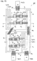
- Fig. 13 shows a schematic planar structure of a power module 20T according to the embodiment (after the semiconductor chips are mounted).
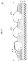
- Fig. 14 shows a schematic cross-sectional structure taken in the line V-V of Fig. 13 .
- Each of the configurations shown in Figs. 13 and 14 corresponds to a power module having a 2-in-1 configuration.
- a flywheel diode 14 4 and an IGBT 13 4 are respectively disposed, via solders 2 under the chip, on a metallic plate 3 2 connected to a leadframe (upper arm) 18 1 (O).
- a first adhesive insulating layer 10 and a second adhesive insulating layer 11 are respectively disposed on the metallic plate 3 2
- a metallic land 5 for main electrode wiring is further disposed on the first adhesive insulating layer 10
- metallic lands 7 1 , 7 2 for signal wiring are further disposed on the second adhesive insulating layer 11.
- a bonding wire 4 connects between an emitter E4 of the IGBT (Q4) 13 4 , and an anode A4 of the flywheel diode (D4) 14 4 .
- a bonding wire 4 (AN) connects between the anode A4 of the flywheel diode (D4) 14 4 , and the metallic land 5 for main electrode wiring.
- a bonding wire 6 (6 1 ) connects between a gate G4 of the IGBT (Q4) 13 4 and the metallic land 7 1 for signal wiring and a bonding wires 6 (6 2 ) connects between an emitter E4 of the IGBT (Q4) 13 4 , and the metallic land 7 2 for signal wiring.
- Fig. 15 shows a schematic circuit representation of the 2-in-1 module corresponding to Fig. 13 , which is the power module 20T according to the embodiment to which the IGBT is applied as the semiconductor device.
- two IGBTs Q1, Q4 are built in one module.
- Reference numeral G1 denotes a gate signal terminal of the IGBT Q1
- reference numeral E1 denotes an emitter terminal of the IGBT Q1.
- Reference numeral C1 denotes a collector terminal of the IGBT Q1.
- Reference numeral G4 denotes a gate signal terminal of the IGBT Q4, reference numeral E4 is an emitter terminal of the IGBT Q4, and reference numeral C4 denotes a collector terminal of the IGBT Q4.
- the collector terminal C1 of the IGBT Q1 is connected to the leadframe (upper arm) 18 2 (P).
- the emitter terminal E1 of the IGBT Q1 and the collector terminal C4 of the IGBT Q4 are connected to the leadframe (lower arm) 18 1 (O).
- the emitter terminal E4 of the IGBT Q4 is connected to a leadframe 19 (N).
- Reference numeral P denotes a positive side power input terminal
- reference numeral N denotes a negative side power input terminal
- reference numeral O denotes an output terminal.
- the collector terminal C1 of the IGBT Q1 is connected to a collector connecting electrode 3 1 , and is connected to the leadframe (upper arm) 18 2 (P) via a bonding wire 34 4 .
- the emitter terminal E1 of the IGBT Q1 and the collector terminal C4 of the IGBT Q4 are connected to the collector connecting electrode 3 2 , and are connected to the leadframe (lower arm) 18 1 (O) via a bonding wire 34 1 .
- the emitter terminal E4 of the IGBT Q4 is connected to the leadframe 19 (N) via the anode terminal A4 of the flywheel diode D4 and bonding wires 4(AN), 34 2 , 34 5 .
- the power module 20T includes: an insulating layer (s) 12; metallic plates 3 1 , 3 2 disposed on the insulating layer(s) 12; a semiconductor device (IGBTs 13 1 , 13 2 , and flywheel diodes 14 1 , 14 2 ) disposed on the metallic plate 3 1 ; a semiconductor device (IGBTs 13 3 , 13 4 , and flywheel diodes 14 3 , 14 4 ) disposed on the metallic plate 3 2 ; first adhesive insulating layers 10 and second adhesive insulating layers 11 respectively disposed on the metallic plates 3 1 , 3 2 ; metallic lands 5 for main electrode wiring respectively disposed on the first adhesive insulating layers 10; and metallic lands 7 1 , 7 2 for signal wiring respectively disposed on the second adhesive insulating layers 11, and a metallic land 7 3 for power wiring disposed on the second adhesive insulating layer 11.
- the metallic land 5 for main electrode wiring and the metallic lands 7 1 , 7 2 for signal wiring having other wiring patterns via the adhesive insulating layers (10, 11) are formed on the metallic plate 3 1 having a wiring pattern on which the semiconductor device (IGBT 13 1 , 13 2 , and flywheel diodes 14 1 , 14 2 ) is mounted.
- the metallic land 5 for main electrode wiring and the metallic lands 7 1 , 7 2 for signal wiring having other wiring patterns via the adhesive insulating layers (10, 11) are formed on the metallic plate 3 2 having a wiring pattern on which the semiconductor device (IGBT 13 4 , and flywheel diodes 14 3 , 14 4 ) is mounted.
- the first adhesive insulating layer 10 and the second adhesive insulating layer 11 are formed of an inorganic adhesive agent.
- the inorganic adhesive agent contains a filler
- the filler may be silica, alumina, zirconia, or a complex thereof, for example.
- the metallic plates 3 1 , 3 2 can be formed of one selected from the group consist of copper, aluminum (aluminium), a copper alloy and an aluminum alloy (aluminium alloy).
- the power module 20T includes: bonding wires 4 (AN) configured to electrically connect respectively between the flywheel diodes 14 3 , 14 4 and the metallic land 5 for main electrode wiring; bonding wires 4 (EA) configured to electrically connect respectively between the IGBTs 13 4 and the flywheel diodes 14 3 , 14 4 ; bonding wires 6 configured to electrically connect respectively between the IGBTs 13 4 and the metallic lands 7 1 , 7 2 for signal wiring; bonding wires 4 (AO) configured to electrically connect respectively between the flywheel diodes 14 1 , 14 2 and the metallic land 5 for main electrode wiring; bonding wires 4 (EA) configured to electrically connect respectively between the IGBTs 13 1 , 13 2 and the flywheel diodes 14 1 , 14 1 ; bonding wire 6 configured to electrically connect respectively between the IGBTs 13 1 , 13 2 and the metallic lands 7 1 , 7 2 for signal wiring; a bonding wire 34 1 configured
- the first adhesive insulating layer 10 and the second adhesive insulating layer 11 in the power module 20T may be formed of the heat-resistant insulating sheet in the same manner as the power module 20 according to the modified example of the embodiment shown in Figs. 5 and 6 .
- the heat-resistant insulating sheet may be formed of one selected from the group consist of an epoxy based resin and a polyimide based resin, for example.
- the thickness of the heat-resistant insulating sheet is approximately 30 ⁇ m to approximately 120 ⁇ m, for example, and therefore the heat-resistant insulating sheet is relatively thin as one layer. Accordingly, the heat-resistant insulating sheet may be formed of a multilayered sheet.
- the power module 20T includes: metallic plates 3 1 , 3 2 divided from each other; a semiconductor device (IGBT 13 1 , 13 2 , and flywheel diodes 14 1 , 14 2 ) disposed on the metallic plate 3 1 via solder 2 under the chip; and a semiconductor device (IGBT 13 4 , and flywheel diodes 14 3 , 14 4 ) disposed on the metallic plate 3 2 via the solder 2 under the chip.
- the IGBT 13 1 , 13 2 (two pieces of the chips) are disposed in parallel on the metallic plate 3 1
- the flywheel diodes 14 1 , 14 2 are also disposed in parallel on the metallic plate 3 1 .
- the respective flywheel diodes 14 1 , 14 2 are connected in reversely parallel to the respective IGBT 13 1 , 13 2 .
- the IGBT 13 4 (two pieces of the chips) are disposed in parallel on the metallic plate 3 2
- the flywheel diodes 14 3 , 14 4 (two pieces of the chips) are also disposed in parallel on the metallic plate 32.
- the respective flywheel diodes 14 3 , 14 4 are connected in reversely parallel to the respective IGBT 13 4 .
- the semiconductor device (IGBT 13 4 , and flywheel diodes 14 3 , 14 4 ) is bonded to the metallic plate 3 2 , to which the leadframe (lower arm) 18 1 (O) is connected, via the solder 2 under the chip, and the semiconductor device (IGBT 13 1 , 13 2 , and flywheel diodes 14 1 , 14 2 ) is similarly bonded to the metallic plate 3 1 , to which the leadframe (upper arm) 18 2 (P) is connected, via the solder 2 under the chip, and then the wiring is performed using the bonding wires 34 1 , 34 2 , 34 3 , 34 4 .
- the power module in the state shown in Figs. 13 and 14 is set on a metallic mold for transfer molding (not shown), and then is molded using the mold resin 17. More specifically, although illustration is omitted in Figs. 13 and 14 , the metallic plates 3 1 , 3 2 ; the first adhesive insulating layer 10 and the second adhesive insulating layer; the metallic land 5 for main electrode wiring and the metallic lands 7 1 , 7 2 for signal wiring; the metallic land 7 3 for power wiring; the semiconductor device (IGBT 13 1 , 13 2 , and flywheel diodes 14 1 , 14 2 ) ; the semiconductor device (IGBT 13 4 , and flywheel diodes 14 3 , 14 4 ); and the bonding wires 4(EA), 4 (AN), 4 (AO), the bonding wire 6 and the bonding wires 34 1 , 34 2 , 34 3 , 34 4 , 34 5 are molded with the mold resin 17 in the same manner as example shown in Figs. 11 and 12 .
- the insulating layer 12 is formed on the back side surface of the metallic plates 3 1 , 3 2 .
- the power module 20T may include a cooling plate (heat sink) 100, and the insulating layer 12 may be disposed at the cooling plate side, in the same manner as example shown in Fig. 11 .
- the insulating layer 12 may include: a relatively-hard insulating layer 12a disposed at the metallic plate 3 1 , 3 2 side; and a relatively-soft insulating layer 12b disposed at the side opposite to the metallic plates 3 1 , 3 2 , in the same manner as example shown in Fig. 12 .
- the power module 20 may include a cooling plate (heat sink) 100, and the relatively-soft insulating layer 12b may be disposed at the cooling plate (heat sink) 100 side, in the same manner as example shown in Fig. 12 .
- the metallic plates 3 1 , 3 2 may be connected to each other with a resin connecting plate (not shown). Even if a force at the time of molding is applied on the bonding wires which are bonded to the semiconductor device etc. , bonding portions are not damaged, thereby improving a reliability of manufacturing.
- the resin connecting plate has a thermal resistance equal to or higher than a molding temperature of the mold resin 17.
- the resin connecting plate may be connected to between the metallic plates 3 1 , 3 2 via a screw.
- the resin connecting plate may be formed of one selected from the group consist of polyphenyl sulfide (PPS), polyethyl ethyl ketone (PEEK), and polyimide (PI).
- PPS polyphenyl sulfide
- PEEK polyethyl ethyl ketone
- PI polyimide
- a notch protruding portion
- a notch hole concave region engaged to the notch (protruding portion) 29 may be formed on the opposed metallic plates 3 1 , 3 2 . According to such a configuration, a positional displacement in a direction of rotation due to the screwing by using the screw can be reduced, thereby achieving more precise positioning of the circuit pattern.
- the wiring pattern can be fixed by bonding on the metallic plates, e.g. a copper plate, with the inorganic adhesive agent etc., instead of the ceramics substrate required for the comparative example.
- the power modules 20, 20T by using such a circuit substrate, substrates which had to be purchased from board maker, etc. can be made on one's own, thereby reducing a member cost. Moreover, a substrate template required for every circuit pattern becomes unnecessary, thereby reducing the substrate template cost. Moreover, since the area of the insulating layer with a small thermal expansion coefficient relatively decreases, a variation in the thickness of the under chip solder decreases, thereby reducing warpages of the whole substrate, and realizing stabilization of the quality.
- the wiring pattern can be fixed by bonding on the metallic plates, e.g. a copper plate, with the inorganic adhesive agent etc. , instead of the ceramics substrate.
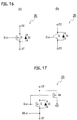
- Fig. 16(a) shows a schematic circuit representative of an SiC MOSFET of the 1-in-1 module, which is the power module 20 according to the embodiment.
- Fig. 16(b) shows a schematic circuit representation of the IGBT of the 1-in-1 module.
- a diode DI connected in reversely parallel to the MOSFET Q is shown in Fig. 16(a) .
- a main electrode of the MOSFET Q is expressed with a drain terminal DT and a source terminal ST.
- a diode DI connected in reversely parallel to the IGBT Q is shown in Fig. 16(b) .
- a main electrode of the IGBT Q is expressed with a collector terminal CT and an emitter terminal ET.
- Fig. 17 shows a detailed circuit representative of the SiC MOSFET of the 1-in-1 module, which is the power module 20 according to the embodiment.
- the power module 20 includes a configuration of 1-in-1 module, for example. More specifically, one piece of the MOSFET Q is included in one module. As an example, five chips (MOSFET ⁇ 5) can be mounted thereon, and a maximum of five pieces of the MOSFETs respectively can be connected to one another in parallel. Note that it is also possible to mount a part of five pieces of the chips for the diode DI thereon.
- a sense MOSFET Qs is connected to the MOSFET Q in parallel.
- the sense MOSFET Qs is formed as a minuteness transistor in the same chip as the MOSFET Q.
- reference numeral SS denotes a source sense terminal
- reference numeral CS denotes a current sense terminal
- reference numeral G denotes a gate signal terminal.
- the sense MOSFET Qs is formed as a minuteness transistor in the same chip.
- Fig. 18(a) shows a schematic circuit representative of the SiC MOSFET of the 1-in-1 module, which is the power module 20T according to the embodiment.
- Reference numeral G1 denotes a gate signal terminal of the MOSFET Q1
- reference numeral S1 denotes a source terminal of the MOSFET Q1.
- Reference numeral G4 denotes a gate signal terminal of the MOSFET Q4, and reference numeral S4 denotes a source terminal of the MOSFET Q4.
- Reference numeral P denotes a positive side power input terminal
- reference numeral N denotes a negative side power input terminal
- reference numeral O denotes an output terminal.
- Fig. 18(b) shows a schematic circuit representative of the 2-in-1 module, which is the power module 20 according to the embodiment.
- two IGBTs Q1, Q4 are built in one module.
- Reference numeral G1 denotes a gate signal terminal of the IGBT Q1
- reference numeral E1 denotes an emitter terminal of the IGBT Q1.
- Reference numeral G4 denotes a gate signal terminal of the IGBT Q4, and reference numeral E4 denotes an emitter terminal of the IGBT Q4.
- Reference numeral P denotes a positive side power input terminal
- reference numeral N denotes a negative side power input terminal
- reference numeral O denotes an output terminal.
- Fig. 19(a) shows a schematic cross-sectional structure of an SiC MOSFET, which is an example of a semiconductor device applied to the power module 20T according to the embodiment.
- Fig. 19(b) shows a schematic cross-sectional structure of the IGBT.
- a schematic cross-sectional structure of the SiC MOSFET as an example of the semiconductor device 110 (Q) applied to the power module 20T includes: a semiconductor substrate 126 composed of an n - type high resistivity layer; a p type base region 128 formed on the surface side of the semiconductor substrate 126; source regions 130 formed on the surface of the p type base regions 128; a gate insulating film 132 disposed on the surface of the semiconductor substrate 126 between the p type base regions 128; a gate electrode 138 disposed on the gate insulating film 132; a source electrode 134 connected to the source region 130 and the p type base region 128; an n + drain region 124 disposed on a back side surface opposite to the surface of the semiconductor substrate 126; and a drain pad electrode 136 connected to the n + drain region 124.
- the semiconductor device 110 is composed of a planar-gate-type n channel vertical SiC-MOSFET, the semiconductor device 110 may be composed of a trench-gate-type n channel vertical SiC-MOSFET, etc.
- GaN based FET etc. instead of SiC MOSFET are also applicable to the semiconductor device 110 (Q) applied to the power module 20T according to the embodiment.
- any one of an SiC based power device, a GaN based power device, and an AlN based power device is applicable to the semiconductor device 110 applied to the power module 20 according to the embodiment.
- a semiconductor of which the bandgap energy is from 1.1 eV to 8 eV, for example, can be used for the semiconductor device 110 applied to the power module 20 according to the embodiment.
- a schematic cross-sectional structure of the IGBT as an example of the semiconductor device 110A (Q) applied to the power module 20T includes: a semiconductor substrate 126 composed of an n - type high resistivity layer; a p type base region 128 formed on the surface side of the semiconductor substrate 126; an emitter region 130E formed on the surface of the p type base region 128; a gate insulating film 132 disposed on the surface of the semiconductor substrate 126 between the p type base regions 128; a gate electrode 138 disposed on the gate insulating film 132; an emitter electrode 134E connected to the emitter region 130E and the p type base region 128; a p + collector region 124P disposed on a back side surface opposite to the surface of the semiconductor substrate 126; and a collector pad electrode 136C connected to the p + collector region 124P.
- the semiconductor device 110 is composed of a planar-gate-type n channel vertical IGBT, the semiconductor device 110 may be composed of a trench-gate-type n channel vertical IGBT, etc.
- Fig. 20 shows a schematic cross-sectional structure of an SiC MOSFET including a source pad electrode SP and a gate pad electrode GP, which is an example of the semiconductor device 110 applied to the power module 20T according to the embodiment.
- the gate pad electrode GP is connected to the gate electrode 138 disposed on the gate insulating film 132, and the source pad electrode SP is connected to the source electrode 134 connected to the source region 130 and the p type base region 128.
- the gate pad electrode GP and the source pad electrode SP are disposed on an interlayer insulating film 144 for passivation which covers the surface of the semiconductor device 110.
- Microstructural transistor structure may be formed in the semiconductor substrate 126 below the gate pad electrode GP and the source pad electrode SP in the same manner as the center portion shown in Fig. 19(a) or 20 .
- the source pad electrode SP may be disposed to be extended onto the interlayer insulating film 144 for passivation, also in the transistor structure of the center portion.
- Fig. 21 shows a schematic cross-sectional structure of an IGBT including a source pad electrode SP and a gate pad electrode GP, which is an example of the semiconductor device 110A applied to the power modules 20, 20T according to the embodiment.
- the gate pad electrode GP is connected to the gate electrode 138 disposed on the gate insulating film 132, and the emitter pad electrode EP is connected to the emitter electrode 134E connected to the emitter region 130E and the p type base region 128.
- the gate pad electrode GP and the emitter pad electrode EP are disposed on an interlayer insulating film 144 for passivation which covers the surface of the semiconductor device 110A.
- Microstructural IGBT structure may be formed in the semiconductor substrate 126 below the gate pad electrode GP and the emitter pad electrode EP in the same manner as the center portion shown in Fig. 19(b) or 21 .
- the emitter pad electrode EP may be disposed to be extended onto the interlayer insulating film 144 for passivation, also in the IGBT structure of the center portion.
- Fig. 22(a) shows an example of a circuit configuration in which the SiC MOSFET is applied as a semiconductor device, and a snubber capacitor C is connected between the power terminal PL and the earth terminal (ground terminal) NL, in a schematic circuit configuration of a three-phase AC inverter 140 composed using the power module 20T according to the embodiment.
- Fig. 22 (a) shows an example of a circuit configuration in which the IGBT is applied as a semiconductor device, and a snubber capacitor C is connected between the power terminal PL and the earth terminal (ground terminal) NL, in a schematic circuit configuration of a three-phase AC inverter 140A composed using the power module 20T according to the embodiment.
- Ldi/dt 3 ⁇ 10 9 (A/s)
- a current change di 300A
- a time variation accompanying switching dt 100 ns.
- the three-phase AC inverter 140 includes: a gate drive unit 150; a power module unit 152 connected to the gate drive unit 150; and a three-phase AC motor unit 154.
- U-phase, V-phase, and W-phase inverters are respectively connected to the three-phase AC motor unit 54 so as to correspond to U phase, V phase, and W phase of the three-phase AC motor unit 154, in the power module unit 152.
- the gate drive unit 150 is connected to the SiC MOSFETs Q1, Q4 as shown in Fig. 23
- the gate drive unit 150 is similarly connected also to the SiC MOSFETs Q2, Q5 and the SiC MOSFETs Q3, Q6 (not shown in Fig. 23 ).
- the SiC MOSFETs Q1, Q4, and Q2, Q5, and Q3, Q6 having inverter configurations are connected between a positive terminal (+) and a negative terminal (-) to which the converter 148 in a storage battery (E) 146 is connected. Furthermore, flywheel diodes D1-D6 are respectively connected reversely in parallel between the source and the drain of the SiC MOSFETs Q1-Q6.
- the three-phase power module unit 152 can also be formed also by similarly forming V phase and W phase inverters.
- the three-phase AC inverter 140A includes: a gate drive unit 150A; a power module unit 152A connected to the gate drive unit 150A; and a three-phase AC motor unit 154A.
- U-phase, V-phase, and W-phase inverters are respectively connected to the three-phase AC motor unit 54 so as to correspond to U phase, V phase, and W phase of the three-phase AC motor unit 154A, in the power module unit 152A.
- the gate drive unit 150A is connected to the IGBTs Q1, Q4 as shown in Fig. 24
- the gate drive unit 150A is similarly connected also to the IGBTs Q2, Q5 and the IGBTs Q3, Q6 (not shown in Fig. 24 ).
- the IGBTs Q1, Q4, and Q2, Q5, and Q3, Q6 having inverter configurations are connected between a positive terminal (+) and a negative terminal (-) to which the converter 148A in a storage battery (E) 146A is connected. Furthermore, flywheel diodes D1-D6 are respectively connected reversely in parallel between the emitter and the collector of the IGBTs Q1-Q6.
- the three-phase power module unit 152A can also be formed also by similarly forming V phase and W phase inverters.
- the power module according to the embodiment can be formed as any one selected from the group consist of 1-in-1 module, 2-in-1 module, 4-in-1 module, 6-in-1 module, and 7-in-1 module.
- one semiconductor device selected from the group consist of an IGBT, a diode, ab Si based MOSFET, and an SiC based MOSFET and a GaNFET is applicable to the power module according to the embodiment.
- a power module having reduced cost, reduced warpage of the whole of a substrate, stabilized quality, and improved reliability; and a fabrication method for such a power module.
- the power module according to the present invention can be used for semiconductor modules, e.g. IGBT modules, diode modules, MOS modules (Si, SiC, GaN), etc.
- the power module according to the embodiment can also be used for structures which do not use insulating substrates, e.g. Direct Copper Bond (DBC) in case type modules.
- DBC Direct Copper Bond
Landscapes
- Engineering & Computer Science (AREA)
- Cooling Or The Like Of Semiconductors Or Solid State Devices (AREA)
- Chemical & Material Sciences (AREA)
- Ceramic Engineering (AREA)
- Materials Engineering (AREA)
- Microelectronics & Electronic Packaging (AREA)
- Inverter Devices (AREA)
Abstract
Description
- The present invention described herein relates to a power module and a fabrication method for such a power module. In particular, the present invention relates to a power module having reduced cost, stabilized quality, and improved reliability; and a fabrication method for such a power module.
- Conventionally, there have been known power modules in which a power chip including a semiconductor device such as Insulated Gate Bipolar Transistor (IGBT) is mounted on a leadframe therein, and of which the whole system thereof is molded with resin (Refer to
Patent Literatures -
- Patent Literature 1:
Japanese Patent No. 3201277 - Patent Literature 2:
Japanese Patent Application Laying-Open Publication No. 2005-109100 - The object of the present invention is to provide: a power module having reduced cost, reduced warpage of the whole of a substrate, stabilized quality, and improved reliability; and a fabrication method for such a power module.
- According to one aspect of the present invention, there is provided a power module comprising: an insulating layer; a metallic plate disposed on the insulating layer; a semiconductor device disposed on the metallic plate; a first adhesive insulating layer and a second adhesive insulating layer respectively disposed on the metallic plate; a metallic land for main electrode wiring disposed on the first adhesive insulating layer; and a metallic land for signal wiring disposed on the second adhesive insulating layer.
- According to another aspect of the present invention, there is provided a fabrication method for a power module comprising: forming a metallic plate; forming a semiconductor device via a solder on a surface of the metallic plate; forming a first adhesive insulating layer and a second adhesive insulating layer on the metallic plate; forming a metallic land for main electrode wiring on the first adhesive insulating layer, and forming a metallic land for signal wiring on the second adhesive insulating layer; bonding-connecting between the semiconductor device and the metallic land for main electrode wiring via a first bonding wire; bonding-connecting between the semiconductor device and the metallic land for signal wiring via a second bonding wire; molding the metallic plate, the first adhesive insulating layer, the second adhesive insulating layer, the metallic land for main electrode wiring, the metallic land for signal wiring, the semiconductor device, the first bonding wire, and the second bonding wire using a mold resin; and forming an insulating layer on a back side surface of the metallic plate.
- According to the present invention, there can be provided a power module having reduced cost, reduced warpage of the whole of a substrate, stabilized quality, and improved reliability; and a fabrication method for such a power module.
-
- [
Fig. 1 ] A schematic planar pattern configuration diagram of IGBT of a one-in-one (1-in-1), which is a power module according to a comparative example. - [
Fig. 2 ] A schematic cross-sectional structure diagram taken in the line I-I ofFig. 1 . - [
Fig. 3 ] A schematic planar pattern configuration diagram of IGBT of a 1-in-1 module, which is a power module according to an embodiment. - [
Fig. 4 ] A schematic cross-sectional structure diagram taken in the line II-II ofFig. 3 . - [
Fig. 5 ] A schematic planar pattern configuration diagram of IGBT of a 1-in-1 module, which is a power module according to a modified example of the embodiment. - [
Fig. 6 ] A schematic cross-sectional structure diagram taken in the line III-III ofFig. 5 . - [
Fig. 7 ] An enlarged schematic planar pattern configuration diagram showing a surface portion of a semiconductor device applied to the power modules according to the embodiment and its modified example.- [
Fig. 8 ] (a) A cross-sectional diagram showing a state where asemiconductor device 1 is bonded on acollector connecting electrode 3, (b) a cross-sectional diagram showing a state after disposing anadhesive insulating layer 10 for emitter and anadhesive insulating layer 11 for signal wiring on thecollector connecting electrode 3, (c) a cross-sectional diagram showing a state where ametallic land 5 for emitter wiring andmetallic lands adhesive insulating layer 10 for emitter and theadhesive insulating layer 11 for signal wiring, and then a heating and pressurizing process is performed, and (d) a cross-sectional diagram showing a state where abonding wire 4 for emitter and bonding wires 6 (61, 62) for signal are bonding-connected thereto, in a process chart showing a fabrication method of the power module according to the embodiment.
- [
- [
Fig. 9 ] A schematic planar pattern configuration diagram showing a state where themetallic land 5 for emitter wiring and themetallic lands adhesive insulating layer 10 for emitter and theadhesive insulating layer 11 for signal wiring, in the process chart showing the fabrication method of the power module according to the embodiment. - [
Fig. 10 ] A schematic cross-sectional structure diagram taken in the line IV-IV ofFig. 9 , in a state where themetallic land 5 for emitter wiring and themetallic lands adhesive insulating layer 10 for emitter and theadhesive insulating layer 11 for signal wiring with a heating and pressurizing process, in the process chart showing the fabrication method of the power module according to the embodiment. - [
Fig. 11 ] A cross-sectional diagram showing a state where an insulating layer formed on a back side surface of thecollector connecting electrode 3 subjected to molding is disposed on a heat sink, in the process chart showing the fabrication method of the power module according to the embodiment. - [
Fig. 12 ] A cross-sectional diagram showing a state where a relatively-hard insulating layer and a relatively-soft insulating layer formed on the back side surface of thecollector connecting electrode 3 subjected to molding are disposed on a heat sink, in the process chart showing the fabrication method of the power module according to the embodiment. - [
Fig. 13 ] A schematic planar pattern configuration diagram of IGBT of a two-in-one (2-in-1) module, which is the power module according to the embodiment. - [
Fig. 14 ] A schematic cross-sectional structure diagram taken in the line V-V ofFig. 13 . - [
Fig. 15 ] A schematic circuit representative diagram of the IGBT of 2-in-1 module corresponding toFig. 13 , which is the power module according to the embodiment.- [
Fig. 16 ] (a) A schematic circuit representative diagram showing an SiC metal oxide semiconductor insulated gate field effect transistor (MOSFET), and (b) a schematic circuit representative diagram of the IGBT of the 1-in-1 module, each which is the power module according to the embodiment.
- [
- [
Fig. 17 ] A detail circuit representative diagram of the SiC MOSFET of the 1-in-1 module, which is the power module according to the embodiment.- [
Fig. 18 ] (a) A schematic circuit representative diagram of the SiC MOSFET of the 2-in-1 module, and (b) a schematic circuit representative diagram of the IGBT of the 2-in-1 module, each which is the power module according to the embodiment. - [
Fig. 19 ] (a) A schematic cross-sectional structure diagram of the SiC MOSFET, and (b) a schematic cross-sectional structure diagram of the IGBT, each which is an example of the semiconductor device applied to the power module according to the embodiment.
- [
- [
Fig.20 ] A schematic cross-sectional structure diagram showing an SiC MOSFET including a source pad electrode SP and a gate pad electrode GP, which is an example of the semiconductor device applied to the power module according to the embodiment. - [
Fig. 21 ] A schematic cross-sectional structure diagram of the IGBT including an emitter pad electrode EP and a gate pad electrode GP, which is an example of the semiconductor device applied to the power module according to the embodiment.- [
Fig. 22 ] (a) An example of a circuit configuration in which the SiC MOSFET is applied as a semiconductor device, and a snubber capacitor is connected between a power terminal PL and an earth terminal (ground terminal) NL, and (b) an example of a circuit configuration in which the IGBT is applied as a semiconductor device, and the snubber capacitor is connected between the power terminal PL and the earth terminal (ground terminal) NL, in a schematic circuit configuration of a three-phase AC inverter composed using the power module according to the embodiment.
- [
- [
Fig. 23 ] A schematic circuit configuration diagram of a three-phase AC inverter composed using the power module according to the embodiment to which the SiC MOSFET is applied as the semiconductor device. - [
Fig. 24 ] A schematic circuit configuration diagram of a three-phase AC inverter composed using the power module according to the embodiment to which the IGBT is applied as the semiconductor device. - Next, a certain embodiment of the present invention will be described with reference to drawings. In the description of the following drawings, the identical or similar reference numeral is attached to the identical or similar part. However, it should be noted that the drawings are schematic and the relation between thickness and the plane size and the ratio of the thickness of each component part differs from an actual thing. Therefore, detailed thickness and size should be determined in consideration of the following explanation. Of course, the part from which the relation and ratio of a mutual size differ also in mutually drawings is included.
- Moreover, the embodiment described hereinafter merely exemplifies the device and method for materializing the technical idea of the present invention; and the embodiment of the present invention does not specify the material, shape, structure, placement, etc. of each component part as the following. The embodiment of the present invention may be changed without departing from the spirit or scope of claims.
-
Fig. 1 shows a schematic planar pattern configuration of a 1-in-1 module, which is a power module semiconductor device 2a according to a comparative example. Moreover,Fig. 2 shows a schematic cross-sectional structure taken in the line I-I ofFig. 1 . - In the
power module 20A according to the comparative example, asemiconductor chip 1 is connected to acollector connecting electrode 3 viasolder 2 under the chip, as shown inFigs. 1 and 2 . Abonding wire 4 for emitter is connected to between an emitter electrode of thesemiconductor chip 1 and ametallic land 5 for emitter wiring for the purpose of extraction of a current from an emitter of thesemiconductor chip 1. Moreover, wiring (not shown) for extracting the current from themetallic land 5 for emitter wiring to the outside is constructed to themetallic land 5 for emitter wiring. Moreover, for the purpose of a current control of thesemiconductor chip 1, abonding wire 61 for gate signal is connected to between a gate electrode of thesemiconductor chip 1 and themetallic land 71 for signal wiring, and abonding wire 62 for emitter signal is connected to between the emitter electrode of thesemiconductor chip 1 andmetallic land 72 for emitter signal wiring. - In the embodiment, the
collector connecting electrode 3, themetallic land 5 for emitter wiring, themetallic lands - The
power module 20A according to the comparative example requires a high cost since it is necessary to request fabrication of the insulating substrate to insulating substrate manufacturers. Moreover, if various circuit patterns are required, a substrate template for every circuit pattern is required, thereby taking a high cost. Moreover, warpage may occur in the insulating substrate due to a coefficient thermal expansion (CTE) difference between the ceramics substrate and the copper circuit pattern. -
Fig. 3 is a schematic planar pattern configuration of IGBT of a 1-in-1 module, which is apower module 20 according to an embodiment. Moreover,Fig. 4 shows a schematic cross-sectional structure taken in the line II-II ofFig. 3 . - As shown in
Figs. 3 and 4 , thepower module 20 according to the embodiment includes: aninsulating layer 12; ametallic plate 3 disposed on theinsulating layer 12; asemiconductor device 1 disposed on themetallic plate 3; a firstadhesive insulating layer 10 and a secondadhesive insulating layer 11 respectively disposed on themetallic plate 3; ametallic land 5 for main electrode wiring disposed on the firstadhesive insulating layer 10; andmetallic lands adhesive insulating layer 11. - As shown in
Figs. 3 and 4 , in thepower module 20 according to the embodiment, themetallic land 5 for main electrode wiring and themetallic lands metallic plate 3 having a wiring pattern on which thesemiconductor device 1 is mounted via the first and second adhesive insulating layers (10, 11). The metallic lands 5, 71 and 72 have wiring patterns other than the wiring pattern on themetallic plate 3. - The first adhesive insulating
layer 10 and the second adhesive insulatinglayer 11 are formed with an inorganic adhesive agent, in thepower module 20 according to the embodiment. - In the embodiment, the inorganic adhesive agent contains a filler, and the filler may be one selected from the group consisting of silica, alumina, zirconia, and a complex thereof, for example.
- The
metallic plate 3 can be formed of one selected from the group consist of copper, aluminum (aluminium), a copper alloy and an aluminum alloy (aluminium alloy). - As shown in
Figs. 3 and 4 , thepower module 20 according to the embodiment includes: afirst bonding wire 4 configured to electrically connect between thesemiconductor device 1 and themetallic land 5 for main electrode wiring; asecond bonding wire 6 configured to electrically connect between thesemiconductor device 1 and themetallic lands Figs. 11 and 12 ) for molding the metallic plate, the first and second adhesive insulating layers, the metallic land for main electrode wiring, the metallic land for signal wiring, the semiconductor device, and the first and second bonding wires. -
Fig. 5 is a schematic planar pattern configuration of IGBT of a 1-in-1 module, which is apower module 20 according to a modified example of the embodiment. Moreover,Fig. 6 shows a schematic cross-sectional structure taken in the line III-III ofFig. 5 . - As shown in
Figs. 5 and 6 , each of the first adhesive insulatinglayer 10A and the second adhesive insulatinglayer 11A is formed of a heat-resistant insulating sheet, in thepower module 20 according to the modified example of the embodiment. - In the embodiment, the heat-resistant insulating sheet may be formed of one selected from the group consist of an epoxy based resin and a polyimide based resin, for example. In the present embodiment, the thickness of the heat-resistant insulating sheet is approximately 30 µm to approximately 120 µm, for example, and therefore the heat-resistant insulating sheet is relatively thin as one layer. Accordingly, the heat-resistant insulating sheet may be formed of a multilayered sheet.
-
Fig. 7 shows an enlarged schematic planar pattern configuration of a surface portion of asemiconductor device 1 applied to thepower modules 20 according to the embodiment and its modified example. - As shown in
Fig. 7 , a source pad electrode SP or an emitter pad electrode EP, and a gate pad electrode GP are disposed on the surface of thesemiconductor device 1. Thefirst bonding wire 4 electrically connected to themetallic land 5 for main electrode wiring and thesecond bonding wire 62 connected to themetallic land 72 for signal wiring are connected onto the source pad electrode SP or emitter pad electrode EP. Moreover, thefirst bonding wire 61 connected to themetallic land 71 for signal wiring is connected onto the gate pad electrode GP. In the embodiment, the emitter pad electrode EP is formed on the surface of thesemiconductor device 1 if thesemiconductor device 1 is IGBT, but the source pad electrode SP is formed on the surface of thesemiconductor device 1 if thesemiconductor device 1 is SiC MOSFET. -
Fig. 8(a) shows a cross-sectional structure showing a state where thesemiconductor device 1 is bonded viasolder 2 under the chip on the metallic plate (collector connecting electrode) 3, in a process chart showing a fabrication method of thepower module 20 according to the embodiment. Moreover,Fig. 8(b) shows a cross-sectional structure showing a state after disposing the adhesive insulatinglayer 10 for emitter and the adhesive insulatinglayer 11 for signal wiring on thecollector connecting electrode 3. Moreover,Fig. 8(c) shows a cross-sectional structure showing a state where themetallic land 5 for emitter wiring is mounted on the adhesive insulatinglayer 10 for emitter and themetallic lands layer 11 for signal wiring, and then a heating and pressurizing process is performed. Moreover,Fig. 8(d) shows a cross-sectional structure showing a state where thesemiconductor device 1 and themetallic land 5 for emitter wiring are bonding-connected via thebonding wire 4 for emitter, and thesemiconductor device 1 and themetallic lands - Furthermore, in the process chart showing the fabrication method of the
power module 20 according to the embodiment,Fig. 9 shows a schematic planar pattern configuration in a state where themetallic land 5 for emitter wiring is mounted on the adhesive insulatinglayer 10 for emitter, and themetallic lands layer 11 for signal wiring. - Moreover, in the process chart showing the fabrication method of the
power module 20 according to the embodiment,Fig. 10 shows a schematic cross-sectional structure taken in the line IV-IV ofFig. 9 , in a state where themetallic land 5 for emitter wiring is bonded onto the adhesive insulatinglayer 10 for emitter, and themetallic lands layer 11 for signal wiring, with a heating and pressurizing process. Ahot plate 120 is applicable as a heating method. A thermostatic oven, a hot air dryer, etc. may also be used therefor. Heating processing temperature is approximately 100 degrees C to approximately 200 degrees C, for example. Pressurizing pressure P is approximately 20 kg/cm2, for example. - Moreover, in the process chart showing the fabrication method of the
power module 20 according to the embodiment,Fig. 11 shows a cross-sectional structure showing a state where a relatively-hard insulating layer 12a and a relatively-softinsulating layer 12b already formed on the back side surface of thecollector connecting electrode 3 already subjected to molding using amold resin 17 are disposed on theheat sink 100, after the bonding process shown inFig. 8(d) . - Moreover, in the process chart showing the fabrication method of the
power module 20 according to the embodiment,Fig. 12 shows a cross-sectional structure showing a state where a relatively-hard insulating layer 12a and a relatively-softinsulating layer 12b already formed on the back side surface of thecollector connecting electrode 3 already subjected to molding using amold resin 17 are disposed on theheat sink 100, after the bonding process shown inFig. 8(d) . - As shown in
Figs. 8(a) - 8(d) and9-12 , the fabrication method of thepower module 20 according to the embodiment includes: forming ametallic plate 3; forming asemiconductor device 1 viasolder 2 under the chip on the surface of themetallic plate 3; forming a first adhesive insulatinglayer 10 and a second adhesive insulatinglayer 11 on themetallic plate 3; forming ametallic land 5 for main electrode wiring on the first adhesive insulatinglayer 10, and formingmetallic lands layer 11; bonding-connecting between thesemiconductor device 1 and themetallic land 5 for main electrode wiring via afirst bonding wire 4; bonding-connecting between thesemiconductor device 1 and themetallic lands metallic plate 3, the first adhesive insulatinglayer 10, the second adhesive insulatinglayer 11, themetallic land 5 for main electrode wiring, themetallic lands semiconductor device 1, thefirst bonding wire 4, and the second bonding wires 6 (61, 62) using amold resin 17; and forming an insulatinglayer 12 on a back side surface of themetallic plate 3. - In the embodiment, the step of forming the insulating
layer 12 on the back side surface of themetallic plate 3 may include: forming a relatively-hard insulating layer 12a on the back side surface of themetallic plate 3; and forming a relatively-softinsulating layer 12b on the relatively-hard insulating layer 12a. - Moreover, the step of forming the
metallic land 5 for main electrode wiring on the first adhesive insulatinglayer 10 and forming themetallic lands layer 11 includes a heating and pressurizing process. - Moreover, the first adhesive insulating
layer 10 and the second adhesive insulatinglayer 11 can be formed of an inorganic adhesive agent. - Moreover, the inorganic adhesive agent contains a filler, and the filler may be silica, alumina, zirconia, or a complex thereof, for example.
- Hereinafter, the fabrication method of the
power module 20 according to the embodiment will now be explained in detail. - (a) Firstly, as shown in
Fig. 8(a) , thesemiconductor device 1 is bonded, withsolder 2 under the chip, onto the surface of the desired-sizedmetallic plate 3 including copper or copper alloy. As material(s) of themetallic plate 3 used herein, aluminum (aluminium) or an aluminum alloy (aluminium alloy) as well as copper or a copper alloy may be used. When using copper or a copper alloy, copper or a copper alloy may be used as it is; or nickel plating, silver plating, or gold plating may be applied for preventing oxidation of themetallic plate 3. When using (aluminium) or an aluminum alloy (aluminium alloy), no extra plating process is required if a solder material for aluminum (aluminium) is used. However, when not using such a solder material for aluminum, it is required to apply nickel plating, silver plating, gold plating, etc. - (b) Next, as shown in
Fig. 8(b) , the first adhesive insulatinglayer 10 and the second adhesive insulatinglayer 11 which are composed of an inorganic adhesive agent are coated to the surface of themetallic plate 3 which is already bonded to thesemiconductor device 1 using thesolder 2 under the chip. As the inorganic adhesive agent used herein, an inorganic adhesive agent of which the volume specific resistivity is equal to or greater than 1 × 10⁶Ω•cm may be used in the light of an insulating breakdown voltage performance of the power module. Moreover, as an inorganic filler contained in such an inorganic adhesive agent, it is preferred to use silica, alumina, zirconia, or a complex of such fillers. Moreover, the thickness of such an inorganic adhesive agent may be approximately 10 µm to approximately 1 mm, for example. It is difficult for an inorganic adhesive agent of which the thick is equal to or less than approximately 10 µm to hold an insulating breakdown voltage. Moreover, it is difficult to apply an inorganic adhesive agent of which the thick is equal to or greater than approximately 1 mm since it takes much time to be cured. The thickness of the inorganic adhesive agent may preferably be approximately 200 µm to approximately 500 µm, for example.
In the embodiment, the step of forming the inorganic adhesive agent is as follows. - (b-1) The inorganic adhesive agent is coated on the
metallic plate 3, and then is naturally dried for approximately one day. - (b-2) Next, it is heated from a room temperature to approximately 40 degrees C for one day.
- (b-3) Next, it is heated to approximately 100 degrees C for approximately four hours, for example, to be subjected to curing treatment.
The inorganic adhesive agent can be formed voidlessly through the above-mentioned steps. - (c) Next, as shown in
Figs. 8(c) and9-10 , themetallic land 5 for emitter wiring and themetallic lands layer 10 for emitter and the adhesive insulatinglayer 11 for signal wiring, to be subjected to pressurization / heating and curing. Ahot plate 120 is applicable as a heating method. A thermostatic oven, a hot air dryer, etc. may also be used therefor. Heating processing temperature is approximately 100 degrees C to approximately 200 degrees C, for example. Moreover, the pressurizing pressure P is approximately 20 kg/cm2, for example. - (d) Next, as shown in
Fig. 8(d) , between thesemiconductor device 1 and themetallic land 5 for emitter wiring are connected using an aluminum wire (abonding wire 4 for emitter), and between thesemiconductor device 1 and themetallic lands bonding wires - (e) Next, as shown in
Fig. 11 , molding is performed using themold resin 17. - (f) Next, as shown in
Fig. 11 , the insulatinglayer 12 is formed on the back side surface of thecollector connecting electrode 3, and then is mounted on theheat sink 100. In this point, the relatively-hard insulating layer 12a and the relatively-softinsulating layer 12b may be formed on the back side surface of thecollector connecting electrode 3, and then may be mounted on theheat sink 100. - The
power module 20 according to the embodiment as shown inFigs. 11 and 12 is completed through the above-mentioned fabricating process. - In the
power module 20 according to the embodiment, there is no need of fabricating a substrate template for newly fabricating the insulating substrate even if the number of thesemiconductor devices 1 to be mounted or disposition of the semiconductor devices is changed, since a shape of themetallic land 5 for emitter wiring or themetallic lands - Moreover, the insulating
layer 12 may be formed of an organic insulating resin layer. - Alternatively, the
power module 20 according to the embodiment may include a cooling plate (heat sink) 100 as shown inFigs. 11 and 12 , and the insulatinglayer 12 may be disposed at the cooling plate side. - Alternatively, in the
power module 20 according to the embodiment, as shown inFig. 12 , the insulatinglayer 12 includes: a relatively-hard insulating layer 12a disposed at ametallic plate 3 side; and a relatively-softinsulating layer 12b disposed at a side opposite to themetallic plate 3 side. - Alternatively, as shown in
Fig. 12 , thepower module 20 according to the embodiment may include a cooling plate (heat sink) 100, and the relatively-softinsulating layer 12b may be disposed at the cooling plate (heat sink) 100 side. - In the embodiment, the relatively-soft
insulating layer 12b may be formed of an organic material(s). - Moreover, the relatively-soft
insulating layer 12b may be formed of a silicone based resin(s). - Moreover, the relatively-soft
insulating layer 12b may be filled up with a high thermally-conductive filler. - In the embodiment, the filler with which the relatively-soft
insulating layer 12b is filled up may be at least one selected from the group consist of aluminium oxide, silicon oxide, aluminum nitride, silicon nitride, boron nitride, beryllia, and magnesia. - Similarly, the relatively-hard insulating layer 12a may also be formed of an organic material(s).
- Moreover, the relatively-hard insulating layer 12a may be formed of at least one selected from the group consist of an epoxy based resin, an urethane system resin, an acrylic resin, and a silicone based resin.
- Moreover, the relatively-hard insulating layer 12a may be filled up with a high thermally-conductive filler.
- In the embodiment, the filler with which the relatively-hard insulating layer 12a is filled up may be at least one selected from the group consist of aluminium oxide, silicon oxide, aluminum nitride, silicon nitride, boron nitride, beryllia, and magnesia.
- The thickness of the
power module 20 according to the embodiment molded with themold resin 17 except theheat sink 100 can be thinly formed, e.g., approximately 7 mm. - Each of the configurations shown in
Figs. 8(a) -8(d) and 9-12 corresponds to the fabrication method of the power module having the 1-in-1 configuration. - The fabrication method of the
power module 20 according to the embodiment explained herein is also similarly applicable to apower module 20T according to the embodiment having a 2-in-1 configuration provided with a plurality of themetallic plates Figs. 13-15 mentioned below. -
Fig. 13 shows a schematic planar structure of apower module 20T according to the embodiment (after the semiconductor chips are mounted). Moreover,Fig. 14 shows a schematic cross-sectional structure taken in the line V-V ofFig. 13 . Each of the configurations shown inFigs. 13 and14 corresponds to a power module having a 2-in-1 configuration. - As shown in
Figs. 13 and14 , a flywheel diode 144 and an IGBT 134 are respectively disposed, viasolders 2 under the chip, on ametallic plate 32 connected to a leadframe (upper arm) 181 (O). Moreover, a first adhesive insulatinglayer 10 and a second adhesive insulatinglayer 11 are respectively disposed on themetallic plate 32, ametallic land 5 for main electrode wiring is further disposed on the first adhesive insulatinglayer 10, andmetallic lands layer 11. Moreover, a bonding wire 4 (EA) connects between an emitter E4 of the IGBT (Q4) 134, and an anode A4 of the flywheel diode (D4) 144. A bonding wire 4 (AN) connects between the anode A4 of the flywheel diode (D4) 144, and themetallic land 5 for main electrode wiring. A bonding wire 6 (61) connects between a gate G4 of the IGBT (Q4) 134 and themetallic land 71 for signal wiring and a bonding wires 6 (62) connects between an emitter E4 of the IGBT (Q4) 134, and themetallic land 72 for signal wiring. - Moreover,
Fig. 15 shows a schematic circuit representation of the 2-in-1 module corresponding toFig. 13 , which is thepower module 20T according to the embodiment to which the IGBT is applied as the semiconductor device. As shown inFig. 15 , two IGBTs Q1, Q4 are built in one module. Reference numeral G1 denotes a gate signal terminal of the IGBT Q1, and reference numeral E1 denotes an emitter terminal of the IGBT Q1. Reference numeral C1 denotes a collector terminal of the IGBT Q1. Reference numeral G4 denotes a gate signal terminal of the IGBT Q4, reference numeral E4 is an emitter terminal of the IGBT Q4, and reference numeral C4 denotes a collector terminal of the IGBT Q4. The collector terminal C1 of the IGBT Q1 is connected to the leadframe (upper arm) 182 (P). The emitter terminal E1 of the IGBT Q1 and the collector terminal C4 of the IGBT Q4 are connected to the leadframe (lower arm) 181 (O). The emitter terminal E4 of the IGBT Q4 is connected to a leadframe 19 (N). Reference numeral P denotes a positive side power input terminal, reference numeral N denotes a negative side power input terminal, and reference numeral O denotes an output terminal. - The collector terminal C1 of the IGBT Q1 is connected to a
collector connecting electrode 31, and is connected to the leadframe (upper arm) 182 (P) via a bonding wire 344. The emitter terminal E1 of the IGBT Q1 and the collector terminal C4 of the IGBT Q4 are connected to thecollector connecting electrode 32, and are connected to the leadframe (lower arm) 181 (O) via a bonding wire 341. The emitter terminal E4 of the IGBT Q4 is connected to the leadframe 19 (N) via the anode terminal A4 of the flywheel diode D4 and bonding wires 4(AN), 342, 345. - As shown in
Figs. 13-15 , thepower module 20T according to the embodiment includes: an insulating layer (s) 12;metallic plates metallic plate 31; a semiconductor device (IGBTs 133, 134, and flywheel diodes 143, 144) disposed on themetallic plate 32; first adhesive insulatinglayers 10 and second adhesive insulatinglayers 11 respectively disposed on themetallic plates metallic lands 5 for main electrode wiring respectively disposed on the first adhesive insulatinglayers 10; andmetallic lands layers 11, and ametallic land 73 for power wiring disposed on the second adhesive insulatinglayer 11. - As shown in
Figs. 13-15 , in thepower module 20T according to the embodiment, themetallic land 5 for main electrode wiring and themetallic lands metallic plate 31 having a wiring pattern on which the semiconductor device (IGBT 131, 132, and flywheel diodes 141, 142) is mounted. Similarly, themetallic land 5 for main electrode wiring and themetallic lands metallic plate 32 having a wiring pattern on which the semiconductor device (IGBT 134, and flywheel diodes 143, 144) is mounted. - Also in the
power module 20T according to the embodiment, the first adhesive insulatinglayer 10 and the second adhesive insulatinglayer 11 are formed of an inorganic adhesive agent. - In the embodiment, the inorganic adhesive agent contains a filler, and the filler may be silica, alumina, zirconia, or a complex thereof, for example.
- The
metallic plates - As shown in
Figs. 13-15 , the power module 20T according to the embodiment includes: bonding wires 4 (AN) configured to electrically connect respectively between the flywheel diodes 143, 144 and the metallic land 5 for main electrode wiring; bonding wires 4 (EA) configured to electrically connect respectively between the IGBTs 134 and the flywheel diodes 143, 144; bonding wires 6 configured to electrically connect respectively between the IGBTs 134 and the metallic lands 71, 72 for signal wiring; bonding wires 4 (AO) configured to electrically connect respectively between the flywheel diodes 141, 142 and the metallic land 5 for main electrode wiring; bonding wires 4 (EA) configured to electrically connect respectively between the IGBTs 131, 132 and the flywheel diodes 141, 141; bonding wire 6 configured to electrically connect respectively between the IGBTs 131, 132 and the metallic lands 71, 72 for signal wiring; a bonding wire 341 configured to connect between the leadframe (lower arm) 181 (O) and the metallic plate 32; a bonding wire 342 configured to connect between the metallic land 5 for main electrode wiring and the metallic land 73 for power wiring; a bonding wire 343 configured to connect between the metallic plate 32 and the metallic land 5 for main electrode wiring; a bonding wire 344 configured to connect between the leadframe (upper arm) 182 (P) and the metallic plate 31; and a bonding wire 345 configured to connect the leadframe 19 (N) and the metallic land for power wiring 73. - The first adhesive insulating
layer 10 and the second adhesive insulatinglayer 11 in thepower module 20T may be formed of the heat-resistant insulating sheet in the same manner as thepower module 20 according to the modified example of the embodiment shown inFigs. 5 and 6 . - In the embodiment, the heat-resistant insulating sheet may be formed of one selected from the group consist of an epoxy based resin and a polyimide based resin, for example. In the present embodiment, the thickness of the heat-resistant insulating sheet is approximately 30 µm to approximately 120 µm, for example, and therefore the heat-resistant insulating sheet is relatively thin as one layer. Accordingly, the heat-resistant insulating sheet may be formed of a multilayered sheet.
- As shown in
Fig. 13 , thepower module 20T according to the embodiment includes:metallic plates metallic plate 31 viasolder 2 under the chip; and a semiconductor device (IGBT 134, and flywheel diodes 143, 144) disposed on themetallic plate 32 via thesolder 2 under the chip. The IGBT 131, 132 (two pieces of the chips) are disposed in parallel on themetallic plate 31, and the flywheel diodes 141, 142 (two pieces of the chips) are also disposed in parallel on themetallic plate 31. The respective flywheel diodes 141, 142 are connected in reversely parallel to the respective IGBT 131, 132. Similarly, the IGBT 134 (two pieces of the chips) are disposed in parallel on themetallic plate 32, and the flywheel diodes 143, 144 (two pieces of the chips) are also disposed in parallel on themetallic plate 32. The respective flywheel diodes 143, 144 are connected in reversely parallel to the respective IGBT 134. - More specifically, the semiconductor device (IGBT 134, and flywheel diodes 143, 144) is bonded to the
metallic plate 32, to which the leadframe (lower arm) 181 (O) is connected, via thesolder 2 under the chip, and the semiconductor device (IGBT 131, 132, and flywheel diodes 141, 142) is similarly bonded to themetallic plate 31, to which the leadframe (upper arm) 182 (P) is connected, via thesolder 2 under the chip, and then the wiring is performed using the bonding wires 341, 342, 343, 344. - Next, the power module in the state shown in
Figs. 13 and14 is set on a metallic mold for transfer molding (not shown), and then is molded using themold resin 17. More specifically, although illustration is omitted inFigs. 13 and14 , themetallic plates layer 10 and the second adhesive insulating layer; themetallic land 5 for main electrode wiring and themetallic lands metallic land 73 for power wiring; the semiconductor device (IGBT 131, 132, and flywheel diodes 141, 142) ; the semiconductor device (IGBT 134, and flywheel diodes 143, 144); and the bonding wires 4(EA), 4 (AN), 4 (AO), thebonding wire 6 and the bonding wires 341, 342, 343, 344, 345 are molded with themold resin 17 in the same manner as example shown inFigs. 11 and 12 . - Subsequently, the insulating
layer 12 is formed on the back side surface of themetallic plates - Alternatively, the
power module 20T according to the embodiment may include a cooling plate (heat sink) 100, and the insulatinglayer 12 may be disposed at the cooling plate side, in the same manner as example shown inFig. 11 . - Alternatively, the insulating
layer 12 may include: a relatively-hard insulating layer 12a disposed at themetallic plate insulating layer 12b disposed at the side opposite to themetallic plates Fig. 12 . - Alternatively, the
power module 20 may include a cooling plate (heat sink) 100, and the relatively-softinsulating layer 12b may be disposed at the cooling plate (heat sink) 100 side, in the same manner as example shown inFig. 12 . - In the
power module 20T according to the embodiment, themetallic plates mold resin 17. Moreover, the resin connecting plate may be connected to between themetallic plates - Moreover, the resin connecting plate may be formed of one selected from the group consist of polyphenyl sulfide (PPS), polyethyl ethyl ketone (PEEK), and polyimide (PI). When the
power module 20T in the state shown inFig. 13 is set on the metallic mold for transfer molding (not shown) and then is molded using themold resin 17, the resin connecting plate is also subjected to the resin molding as it is. - Although illustration is omitted, a notch (protruding portion) may be provided on a plane of the resin connecting plate opposite to the
metallic plate metallic plates - In the
power modules - In the
power modules - Hereinafter, there will now be explained examples of the
power modules power modules -
Fig. 16(a) shows a schematic circuit representative of an SiC MOSFET of the 1-in-1 module, which is thepower module 20 according to the embodiment.Fig. 16(b) shows a schematic circuit representation of the IGBT of the 1-in-1 module. - A diode DI connected in reversely parallel to the MOSFET Q is shown in
Fig. 16(a) . A main electrode of the MOSFET Q is expressed with a drain terminal DT and a source terminal ST. Similarly, a diode DI connected in reversely parallel to the IGBT Q is shown inFig. 16(b) . A main electrode of the IGBT Q is expressed with a collector terminal CT and an emitter terminal ET. - Moreover,
Fig. 17 shows a detailed circuit representative of the SiC MOSFET of the 1-in-1 module, which is thepower module 20 according to the embodiment. - The
power module 20 according to the embodiment includes a configuration of 1-in-1 module, for example. More specifically, one piece of the MOSFET Q is included in one module. As an example, five chips (MOSFET × 5) can be mounted thereon, and a maximum of five pieces of the MOSFETs respectively can be connected to one another in parallel. Note that it is also possible to mount a part of five pieces of the chips for the diode DI thereon. - More particularly, as shown in
Fig. 17 , a sense MOSFET Qs is connected to the MOSFET Q in parallel. The sense MOSFET Qs is formed as a minuteness transistor in the same chip as the MOSFET Q. InFig. 17 , reference numeral SS denotes a source sense terminal, reference numeral CS denotes a current sense terminal, and reference numeral G denotes a gate signal terminal. Note that, also in the semiconductor chip Q according to the embodiment, the sense MOSFET Qs is formed as a minuteness transistor in the same chip. - Moreover,
Fig. 18(a) shows a schematic circuit representative of the SiC MOSFET of the 1-in-1 module, which is thepower module 20T according to the embodiment. - As shown in
Fig. 18(a) , two MOSFETs Q1, Q4 are included in one module. Reference numeral G1 denotes a gate signal terminal of the MOSFET Q1, and reference numeral S1 denotes a source terminal of the MOSFET Q1. Reference numeral G4 denotes a gate signal terminal of the MOSFET Q4, and reference numeral S4 denotes a source terminal of the MOSFET Q4. Reference numeral P denotes a positive side power input terminal, reference numeral N denotes a negative side power input terminal, and reference numeral O denotes an output terminal. - Moreover,
Fig. 18(b) shows a schematic circuit representative of the 2-in-1 module, which is thepower module 20 according to the embodiment. As shown inFig. 18(b) , two IGBTs Q1, Q4 are built in one module. Reference numeral G1 denotes a gate signal terminal of the IGBT Q1, and reference numeral E1 denotes an emitter terminal of the IGBT Q1. Reference numeral G4 denotes a gate signal terminal of the IGBT Q4, and reference numeral E4 denotes an emitter terminal of the IGBT Q4. Reference numeral P denotes a positive side power input terminal, reference numeral N denotes a negative side power input terminal, and reference numeral O denotes an output terminal. -
Fig. 19(a) shows a schematic cross-sectional structure of an SiC MOSFET, which is an example of a semiconductor device applied to thepower module 20T according to the embodiment.Fig. 19(b) shows a schematic cross-sectional structure of the IGBT. - As shown in
Fig. 19(a) , a schematic cross-sectional structure of the SiC MOSFET as an example of the semiconductor device 110 (Q) applied to thepower module 20T according to the embodiment includes: asemiconductor substrate 126 composed of an n- type high resistivity layer; a ptype base region 128 formed on the surface side of thesemiconductor substrate 126;source regions 130 formed on the surface of the ptype base regions 128; agate insulating film 132 disposed on the surface of thesemiconductor substrate 126 between the ptype base regions 128; agate electrode 138 disposed on thegate insulating film 132; asource electrode 134 connected to thesource region 130 and the ptype base region 128; an n+ drain region 124 disposed on a back side surface opposite to the surface of thesemiconductor substrate 126; and adrain pad electrode 136 connected to the n+ drain region 124. - In
Fig. 19(a) , although thesemiconductor device 110 is composed of a planar-gate-type n channel vertical SiC-MOSFET, thesemiconductor device 110 may be composed of a trench-gate-type n channel vertical SiC-MOSFET, etc. - Moreover, a GaN based FET etc. instead of SiC MOSFET are also applicable to the semiconductor device 110 (Q) applied to the
power module 20T according to the embodiment. - Any one of an SiC based power device, a GaN based power device, and an AlN based power device is applicable to the
semiconductor device 110 applied to thepower module 20 according to the embodiment. - Furthermore, a semiconductor of which the bandgap energy is from 1.1 eV to 8 eV, for example, can be used for the
semiconductor device 110 applied to thepower module 20 according to the embodiment. - Similarly, as shown in
Fig. 19(b) , a schematic cross-sectional structure of the IGBT as an example of thesemiconductor device 110A (Q) applied to thepower module 20T according to the embodiment includes: asemiconductor substrate 126 composed of an n- type high resistivity layer; a ptype base region 128 formed on the surface side of thesemiconductor substrate 126; anemitter region 130E formed on the surface of the ptype base region 128; agate insulating film 132 disposed on the surface of thesemiconductor substrate 126 between the ptype base regions 128; agate electrode 138 disposed on thegate insulating film 132; anemitter electrode 134E connected to theemitter region 130E and the ptype base region 128; a p+ collector region 124P disposed on a back side surface opposite to the surface of thesemiconductor substrate 126; and acollector pad electrode 136C connected to the p+ collector region 124P. - In
Fig. 19(b) , although thesemiconductor device 110 is composed of a planar-gate-type n channel vertical IGBT, thesemiconductor device 110 may be composed of a trench-gate-type n channel vertical IGBT, etc. -
Fig. 20 shows a schematic cross-sectional structure of an SiC MOSFET including a source pad electrode SP and a gate pad electrode GP, which is an example of thesemiconductor device 110 applied to thepower module 20T according to the embodiment. The gate pad electrode GP is connected to thegate electrode 138 disposed on thegate insulating film 132, and the source pad electrode SP is connected to thesource electrode 134 connected to thesource region 130 and the ptype base region 128. - Moreover, as shown in
Fig. 20 , the gate pad electrode GP and the source pad electrode SP are disposed on aninterlayer insulating film 144 for passivation which covers the surface of thesemiconductor device 110. Microstructural transistor structure may be formed in thesemiconductor substrate 126 below the gate pad electrode GP and the source pad electrode SP in the same manner as the center portion shown inFig. 19(a) or20 . - Furthermore, as shown in
Fig. 20 , the source pad electrode SP may be disposed to be extended onto theinterlayer insulating film 144 for passivation, also in the transistor structure of the center portion. -
Fig. 21 shows a schematic cross-sectional structure of an IGBT including a source pad electrode SP and a gate pad electrode GP, which is an example of thesemiconductor device 110A applied to thepower modules gate electrode 138 disposed on thegate insulating film 132, and the emitter pad electrode EP is connected to theemitter electrode 134E connected to theemitter region 130E and the ptype base region 128. - Moreover, as shown in
Fig. 21 , the gate pad electrode GP and the emitter pad electrode EP are disposed on aninterlayer insulating film 144 for passivation which covers the surface of thesemiconductor device 110A. Microstructural IGBT structure may be formed in thesemiconductor substrate 126 below the gate pad electrode GP and the emitter pad electrode EP in the same manner as the center portion shown inFig. 19(b) or21 . - Furthermore, as shown in
Fig. 21 , the emitter pad electrode EP may be disposed to be extended onto theinterlayer insulating film 144 for passivation, also in the IGBT structure of the center portion. -
Fig. 22(a) shows an example of a circuit configuration in which the SiC MOSFET is applied as a semiconductor device, and a snubber capacitor C is connected between the power terminal PL and the earth terminal (ground terminal) NL, in a schematic circuit configuration of a three-phase AC inverter 140 composed using thepower module 20T according to the embodiment. Similarly,Fig. 22 (a) shows an example of a circuit configuration in which the IGBT is applied as a semiconductor device, and a snubber capacitor C is connected between the power terminal PL and the earth terminal (ground terminal) NL, in a schematic circuit configuration of a three-phase AC inverter 140A composed using thepower module 20T according to the embodiment. - When connecting the
power module 20T according to the embodiment to the power source E, large surge voltage Ldi/dt is produced by an inductance L included in a connection line due to a high switching speed of the SiC MOSFET and IGBT. For example, the surge voltage Ldi/dt is expressed as follows: Ldi/dt = 3×10⁹ (A/s), where a current change di=300A, and a time variation accompanying switching dt = 100 ns. Although a value of the surge voltage Ldi/dt changes dependent on a value of the inductance L, the surge voltage Ldi/dt is superimposed on the power source V. Such a surge voltage Ldi/dt can be absorbed by the snubber capacitor C connected between the power terminal PL and the earth terminal (ground terminal) NL. - Next, there will now be explained the three-
phase AC inverter 140 composed using thepower module 20T according to the embodiment to which the SiC MOSFET is applied as the semiconductor device, with reference toFig. 23 . - As shown in
Fig. 23 , the three-phase AC inverter 140 includes: agate drive unit 150; apower module unit 152 connected to thegate drive unit 150; and a three-phaseAC motor unit 154. U-phase, V-phase, and W-phase inverters are respectively connected to the three-phase AC motor unit 54 so as to correspond to U phase, V phase, and W phase of the three-phaseAC motor unit 154, in thepower module unit 152. In this case, although thegate drive unit 150 is connected to the SiC MOSFETs Q1, Q4 as shown inFig. 23 , thegate drive unit 150 is similarly connected also to the SiC MOSFETs Q2, Q5 and the SiC MOSFETs Q3, Q6 (not shown inFig. 23 ). - In the
power module unit 152, the SiC MOSFETs Q1, Q4, and Q2, Q5, and Q3, Q6 having inverter configurations are connected between a positive terminal (+) and a negative terminal (-) to which theconverter 148 in a storage battery (E) 146 is connected. Furthermore, flywheel diodes D1-D6 are respectively connected reversely in parallel between the source and the drain of the SiC MOSFETs Q1-Q6. - Although the structure of the single phase inverter corresponding to U phase portion of
Fig. 23 has been explained in thepower module 20T according to the embodiment, the three-phasepower module unit 152 can also be formed also by similarly forming V phase and W phase inverters. - Next, there will now be explained the three-
phase AC inverter 140A composed using thepower module 20T according to the embodiment to which the IGBT is applied as the semiconductor device, with reference toFig. 24 . - As shown in
Fig. 24 , the three-phase AC inverter 140A includes: agate drive unit 150A; apower module unit 152A connected to thegate drive unit 150A; and a three-phaseAC motor unit 154A. U-phase, V-phase, and W-phase inverters are respectively connected to the three-phase AC motor unit 54 so as to correspond to U phase, V phase, and W phase of the three-phaseAC motor unit 154A, in thepower module unit 152A. In this case, although thegate drive unit 150A is connected to the IGBTs Q1, Q4 as shown inFig. 24 , thegate drive unit 150A is similarly connected also to the IGBTs Q2, Q5 and the IGBTs Q3, Q6 (not shown inFig. 24 ). - In the
power module unit 152A, the IGBTs Q1, Q4, and Q2, Q5, and Q3, Q6 having inverter configurations are connected between a positive terminal (+) and a negative terminal (-) to which theconverter 148A in a storage battery (E) 146A is connected. Furthermore, flywheel diodes D1-D6 are respectively connected reversely in parallel between the emitter and the collector of the IGBTs Q1-Q6. - Although the structure of the single phase inverter corresponding to U phase portion of
Fig. 24 has been explained in thepower module 20T according to the embodiment, the three-phasepower module unit 152A can also be formed also by similarly forming V phase and W phase inverters. - The power module according to the embodiment can be formed as any one selected from the group consist of 1-in-1 module, 2-in-1 module, 4-in-1 module, 6-in-1 module, and 7-in-1 module.
- Moreover, one semiconductor device selected from the group consist of an IGBT, a diode, ab Si based MOSFET, and an SiC based MOSFET and a GaNFET is applicable to the power module according to the embodiment.
- As explained above, according to the present invention, there can be provided a power module having reduced cost, reduced warpage of the whole of a substrate, stabilized quality, and improved reliability; and a fabrication method for such a power module.
- As explained above, the present invention has been described, as a disclosure including associated description and drawings to be construed as illustrative, not restrictive. This disclosure makes clear a variety of alternative embodiment, working examples, and operational techniques for those skilled in the art.
- Such being the case, the present present invention covers a variety of embodiments, whether described or not.
- The power module according to the present invention can be used for semiconductor modules, e.g. IGBT modules, diode modules, MOS modules (Si, SiC, GaN), etc. The power module according to the embodiment can also be used for structures which do not use insulating substrates, e.g. Direct Copper Bond (DBC) in case type modules.
-
- 1, 110, 110A: Semiconductor device (Semiconductor chip)
- 2: Solder under the chip
- 3, 31, 32: Metallic plate (Metallic base, Main electrode connecting electrode, Collector connecting electrode)
- 4: Bonding wire for emitter
- 5: Metallic land for main electrode wiring (Metallic land for emitter wiring)
- 6, 61, 62: Bonding wire for signal
- 7, 71, 72: Metallic land for signal wiring
- 73: Metallic land for power wiring
- 8: Ceramics substrate
- 9: Back surface copper foil
- 10, 10A: Adhesive insulating layer for emitter
- 11, 11A: Adhesive insulating layer for signal wiring
- 12: Insulating layer (Organic insulating resin layer)
- 12a: Relatively-hard insulating layer
- 12b: Relatively-soft insulating layer
- 131, 132, 134: IGBT (Q1-Q6)
- 141, 142, 143, 144 : Flywheel diode (D1-D6)
- 17: Mold resin
- 181, 182, 19: Leadframe
- 20, 20A, 20T: Power module
- 341, 342, 343, 344, 345: Bonding wire
- 100: Cooling plate (Heat sink)
- 120: Hot plate
- 124: Drain region
- 124P: Collector region
- 126: Semiconductor substrate
- 128: P type base region
- 130: Source region
- 130E: Emitter region
- 132: Gate insulating film
- 134: Source electrode
- 134E: Emitter electrode
- 136: Drain pad electrode
- 136C: Collector pad electrode
- 138: Gate electrode
- 144: Interlayer insulating film
Claims (28)
- A power module comprising:an insulating layer;a metallic plate disposed on the insulating layer;a semiconductor device disposed on the metallic plate;a first adhesive insulating layer and a second adhesive insulating layer respectively disposed on the metallic plate;a metallic land for main electrode wiring disposed on the first adhesive insulating layer; anda metallic land for signal wiring disposed on the second adhesive insulating layer.
- The power module according to claim 1, wherein
the first adhesive insulating layer and the second adhesive insulating layer are an inorganic adhesive agent. - The power module according to claim 2, wherein
the inorganic adhesive agent contains a filler, and the filler is one selected from the group consisting of silica, alumina, zirconia, and a complex thereof. - The power module according to claim 1, wherein
the first adhesive insulating layer and the second adhesive insulating layer are a heat-resistant insulating sheet. - The power module according to claim 4, wherein
the heat-resistant insulating sheet is formed of one selected from the group consist of an epoxy based resin and a polyimide based resin. - The power module according to claim 5, wherein
the heat-resistant insulating sheet is formed of a multilayered sheet. - The power module according to any one of claims 1-6, wherein
the metallic plate is formed of one selected from the group consist of copper, aluminum, copper alloy and an aluminum alloy. - The power module according to any one of claims 1-7, further comprising:a first bonding wire configured to electrically connect between the semiconductor device and the metallic land for main electrode wiring; anda second bonding wire configured to electrically connect between the semiconductor device and the metallic land for signal wiring; anda mold resin for molding the metallic plate, the first adhesive insulating layer and the second adhesive insulating layer, the metallic land for main electrode wiring and the metallic land for signal wiring, the semiconductor device, and the first bonding wire and the second bonding wire.
- The power module according to any one of claims 1-8, wherein
the insulating layer comprises a relatively-hard insulating layer disposed at a metallic plate side, and a relatively-soft insulating layer disposed at a side opposite to the metallic plate side. - The power module according to claim 9, further comprising:a cooling plate, whereinthe relatively-soft insulating layer is disposed at a side of the cooling body.
- The power module according to claim 9 or 10, wherein
the relatively-soft insulating layer is formed of an organic material. - The power module according to any one of claims 9-11, wherein
the relatively-soft insulating layer is formed of a silicone based resin. - The power module according to any one of claims 9-12, wherein
the relatively-soft insulating layer is filled up with a high thermally-conductive filler. - The power module according to claim 13, wherein
the filler is at least one selected from the group consist of aluminium oxide, silicon oxide, aluminum nitride, silicon nitride, boron nitride, beryllia, and magnesia. - The power module according to any one of claims 9-14, wherein
the relatively-hard insulating layer is formed of an organic material. - The power module according to any one of claims 9-15, wherein
the relatively-hard insulating layer is formed of at least one selected from the group consist of an epoxy based resin, an urethane system resin, an acrylic resin, and a silicone based resin. - The power module according to any one of claims 9-16, wherein
the relatively-hard insulating layer is filled up with a high thermally-conductive filler. - The power module according to claim 17, wherein
the filler is at least one selected from the group consist of aluminium oxide, silicon oxide, aluminum nitride, silicon nitride, boron nitride, beryllia, and magnesia. - The power module according to any one of claims 1-18, wherein
the power module is formed as any one selected from the group consist of 1-in-1 module, 2-in-1 module, 4-in-1 module, 6-in-1 module, and 7-in-1 module. - The power module according to any one of claims 1-19, wherein
the semiconductor device comprises one selected from the group consist of an IGBT, a diode, an Si based MOSFET, an SiC based MOSFET and a GaNFET. - A fabrication method for a power module comprising:forming a metallic plate;forming a semiconductor device via a solder on a surface of the metallic plate;forming a first adhesive insulating layer and a second adhesive insulating layer on the metallic plate;forming a metallic land for main electrode wiring on the first adhesive insulating layer, and forming a metallic land for signal wiring on the second adhesive insulating layer;bonding-connecting between the semiconductor device and the metallic land for main electrode wiring via a first bonding wire;bonding-connecting between the semiconductor device and the metallic land for signal wiring via a second bonding wire;molding the metallic plate, the first adhesive insulating layer, the second adhesive insulating layer, the metallic land for main electrode wiring, the metallic land for signal wiring, the semiconductor device, the first bonding wire, and the second bonding wire using a mold resin; andforming an insulating layer on a back side surface of the metallic plate.
- The fabrication method for a power module according to claim 21, wherein
the step of forming the insulating layer on the back side surface of the metallic plate comprises: forming a relatively-hard insulating layer on the back side surface of the metallic plate; and
forming a relatively-soft insulating layer on the relatively-hard insulating layer. - The fabrication method for a power module according to claim 21 or 22, wherein
the step of forming the metallic land for main electrode wiring on the first adhesive insulating layer and forming the metallic land for signal wiring on the second adhesive insulating layer comprises a heating and pressurizing process. - The fabrication method for a power module according to any one of claims 21-23, wherein
the first adhesive insulating layer and the second adhesive insulating layer are an inorganic adhesive agent. - The fabrication method for a power module according to claim 24, wherein
the inorganic adhesive agent contains a filler, and the filler is one selected from the group consisting of silica, alumina, zirconia, and a complex thereof. - The fabrication method for a power module according to any one of claims 21-23, wherein
the first adhesive insulating layer and the second adhesive insulating layer are a heat-resistant insulating sheet. - The fabrication method for a power module according to claim 26, wherein
the heat-resistant insulating sheet is formed of one selected from the group consist of an epoxy based resin and a polyimide based resin. - The fabrication method for a power module according to claim 27, wherein
the heat-resistant insulating sheet is formed of a multilayered sheet.
Applications Claiming Priority (2)
| Application Number | Priority Date | Filing Date | Title |
|---|---|---|---|
| JP2013210222A JP2015076442A (en) | 2013-10-07 | 2013-10-07 | Power module and manufacturing method of the same |
| PCT/JP2014/076690 WO2015053219A1 (en) | 2013-10-07 | 2014-10-06 | Power module, and method for producing same |
Publications (3)
| Publication Number | Publication Date |
|---|---|
| EP3057126A1 true EP3057126A1 (en) | 2016-08-17 |
| EP3057126A4 EP3057126A4 (en) | 2017-12-06 |
| EP3057126B1 EP3057126B1 (en) | 2019-09-04 |
Family
ID=52813035
Family Applications (1)
| Application Number | Title | Priority Date | Filing Date |
|---|---|---|---|
| EP14853126.2A Active EP3057126B1 (en) | 2013-10-07 | 2014-10-06 | Power module, and method for producing same |
Country Status (4)
| Country | Link |
|---|---|
| US (1) | US9773720B2 (en) |
| EP (1) | EP3057126B1 (en) |
| JP (1) | JP2015076442A (en) |
| WO (1) | WO2015053219A1 (en) |
Cited By (1)
| Publication number | Priority date | Publication date | Assignee | Title |
|---|---|---|---|---|
| WO2020251842A1 (en) * | 2019-06-14 | 2020-12-17 | Cree Fayetteville, Inc. | Package for power electronics |
Families Citing this family (15)
| Publication number | Priority date | Publication date | Assignee | Title |
|---|---|---|---|---|
| WO2017054855A1 (en) * | 2015-09-30 | 2017-04-06 | Agile Power Switch 3D - Integration Apsi3D | A semiconductor power device comprising additional tracks and method of manufacturing the semiconductor power device |
| JP6466030B2 (en) | 2015-10-29 | 2019-02-06 | アーベーベー・シュバイツ・アーゲー | Semiconductor module |
| JP6743728B2 (en) * | 2017-03-02 | 2020-08-19 | 三菱電機株式会社 | Semiconductor power module and power converter |
| DE112018002579T5 (en) * | 2017-05-19 | 2020-03-19 | Mitsubishi Electric Corporation | SEMICONDUCTOR COMPONENT |
| WO2018221296A1 (en) * | 2017-05-30 | 2018-12-06 | 三菱電機株式会社 | Power conversion device |
| US11211312B2 (en) | 2017-11-20 | 2021-12-28 | Rohm Co., Ltd. | Semiconductor device |
| US11063495B2 (en) | 2019-07-01 | 2021-07-13 | Nidec Motor Corporation | Heatsink clamp for multiple electronic components |
| JP6887476B2 (en) * | 2019-11-05 | 2021-06-16 | 三菱電機株式会社 | Semiconductor power module |
| JPWO2022024572A1 (en) * | 2020-07-27 | 2022-02-03 | ||
| CN113097154B (en) * | 2021-03-22 | 2024-10-29 | 西安交通大学 | A bidirectional switch power module and its preparation method |
| CN113113319B (en) * | 2021-03-23 | 2023-02-10 | 江西新菲新材料有限公司 | Lead frame and manufacturing method thereof |
| JP7603571B2 (en) * | 2021-11-29 | 2024-12-20 | 三菱電機株式会社 | Semiconductor Device |
| FR3140208B1 (en) * | 2022-09-27 | 2024-10-04 | Valeo Equip Electr Moteur | connecting element intended to bring into thermal contact A PART TO BE COOLED AND A HEAT SINK |
| JP7843721B2 (en) * | 2023-02-08 | 2026-04-10 | 三菱電機株式会社 | Semiconductor equipment |
| CN118588645B (en) * | 2024-06-21 | 2025-03-14 | 青岛科芯半导体有限公司 | An IGBT chip and its packaging structure |
Family Cites Families (16)
| Publication number | Priority date | Publication date | Assignee | Title |
|---|---|---|---|---|
| JPS5588356A (en) * | 1978-12-27 | 1980-07-04 | Hitachi Ltd | Semiconductor device |
| JPS61194755A (en) * | 1985-02-25 | 1986-08-29 | Hitachi Ltd | Semiconductor device |
| JPH06334114A (en) * | 1993-03-25 | 1994-12-02 | Toppan Printing Co Ltd | Multichip semiconductor device |
| US5655288A (en) * | 1994-03-25 | 1997-08-12 | Rohm Co., Ltd. | Method of manufacturing a thermal head |
| JP3201277B2 (en) | 1996-09-11 | 2001-08-20 | 株式会社日立製作所 | Semiconductor device |
| JP3972519B2 (en) * | 1999-06-18 | 2007-09-05 | 株式会社日立製作所 | Power semiconductor module |
| US6841857B2 (en) * | 2001-07-18 | 2005-01-11 | Infineon Technologies Ag | Electronic component having a semiconductor chip, system carrier, and methods for producing the electronic component and the semiconductor chip |
| JP4023397B2 (en) * | 2003-04-15 | 2007-12-19 | 富士電機機器制御株式会社 | Semiconductor module and manufacturing method thereof |
| JP2005109100A (en) | 2003-09-30 | 2005-04-21 | Mitsubishi Electric Corp | Semiconductor device and manufacturing method thereof |
| TWI325617B (en) * | 2006-12-18 | 2010-06-01 | Chipmos Technologies Inc | Chip package and method of manufacturing the same |
| US7868465B2 (en) * | 2007-06-04 | 2011-01-11 | Infineon Technologies Ag | Semiconductor device with a metallic carrier and two semiconductor chips applied to the carrier |
| DE102008001414A1 (en) * | 2008-04-28 | 2009-10-29 | Robert Bosch Gmbh | Substrate circuit module with components in multiple contacting levels |
| JP5130173B2 (en) * | 2008-09-25 | 2013-01-30 | 日東シンコー株式会社 | Semiconductor module and semiconductor module manufacturing method |
| JP5071405B2 (en) * | 2009-02-13 | 2012-11-14 | 三菱電機株式会社 | Power semiconductor device |
| JP5863599B2 (en) * | 2012-08-21 | 2016-02-16 | 三菱電機株式会社 | Power module |
| JP2014107519A (en) * | 2012-11-30 | 2014-06-09 | Mitsubishi Electric Corp | Semiconductor device and manufacturing method of the same |
-
2013
- 2013-10-07 JP JP2013210222A patent/JP2015076442A/en active Pending
-
2014
- 2014-10-06 EP EP14853126.2A patent/EP3057126B1/en active Active
- 2014-10-06 WO PCT/JP2014/076690 patent/WO2015053219A1/en not_active Ceased
-
2016
- 2016-04-06 US US15/092,308 patent/US9773720B2/en active Active
Cited By (5)
| Publication number | Priority date | Publication date | Assignee | Title |
|---|---|---|---|---|
| WO2020251842A1 (en) * | 2019-06-14 | 2020-12-17 | Cree Fayetteville, Inc. | Package for power electronics |
| US11069640B2 (en) | 2019-06-14 | 2021-07-20 | Cree Fayetteville, Inc. | Package for power electronics |
| US11756910B2 (en) | 2019-06-14 | 2023-09-12 | Wolfspeed, Inc. | Package for power electronics |
| US11887953B2 (en) | 2019-06-14 | 2024-01-30 | Wolfspeed, Inc. | Package for power electronics |
| US12400986B2 (en) | 2019-06-14 | 2025-08-26 | Wolfspeed, Inc. | Package for power electronics |
Also Published As
| Publication number | Publication date |
|---|---|
| JP2015076442A (en) | 2015-04-20 |
| WO2015053219A1 (en) | 2015-04-16 |
| EP3057126A4 (en) | 2017-12-06 |
| EP3057126B1 (en) | 2019-09-04 |
| US9773720B2 (en) | 2017-09-26 |
| US20160218050A1 (en) | 2016-07-28 |
Similar Documents
| Publication | Publication Date | Title |
|---|---|---|
| EP3057126B1 (en) | Power module, and method for producing same | |
| US9064869B2 (en) | Semiconductor module and a method for fabrication thereof by extended embedding technologies | |
| US9721875B2 (en) | Power module and fabrication method for the same | |
| US7759778B2 (en) | Leaded semiconductor power module with direct bonding and double sided cooling | |
| CN104051376B (en) | Power overlay structure and preparation method thereof | |
| US11908760B2 (en) | Package with encapsulated electronic component between laminate and thermally conductive carrier | |
| US10418313B2 (en) | Electronic module comprising a plurality of encapsulation layers and a method for producing it | |
| EP3026700B1 (en) | Power module and manufacturing method thereof | |
| US11574889B2 (en) | Power module comprising two substrates and method of manufacturing the same | |
| US11171071B2 (en) | Power module and fabrication method of the power module | |
| CN104051363B (en) | Chip package and method for manufacturing the same | |
| JP2009536458A (en) | Semiconductor module and manufacturing method thereof | |
| US9437508B2 (en) | Method for manufacturing semiconductor device and semiconductor device | |
| KR20150058015A (en) | Semiconductor device and method for manufacturing same | |
| CN108346651A (en) | Include the semiconductor module of transistor chip, diode chip for backlight unit and driver chip | |
| US10937767B2 (en) | Chip packaging method and device with packaged chips | |
| US20150270201A1 (en) | Semiconductor module package and method of manufacturing the same | |
| CN106098648B (en) | IGBT heat-radiating substrates and its manufacturing method, IGBT modules and its manufacturing method | |
| US11545874B2 (en) | Thermal management assemblies for electronic assemblies circumferentially mounted around a motor using a flexible substrate | |
| CN106876350B (en) | Power module and manufacturing method thereof | |
| US20180040562A1 (en) | Elektronisches modul und verfahren zu seiner herstellung | |
| JP4961314B2 (en) | Power semiconductor device | |
| JP2010258161A (en) | Manufacturing method of semiconductor device |
Legal Events
| Date | Code | Title | Description |
|---|---|---|---|
| PUAI | Public reference made under article 153(3) epc to a published international application that has entered the european phase |
Free format text: ORIGINAL CODE: 0009012 |
|
| 17P | Request for examination filed |
Effective date: 20160504 |
|
| AK | Designated contracting states |
Kind code of ref document: A1 Designated state(s): AL AT BE BG CH CY CZ DE DK EE ES FI FR GB GR HR HU IE IS IT LI LT LU LV MC MK MT NL NO PL PT RO RS SE SI SK SM TR |
|
| AX | Request for extension of the european patent |
Extension state: BA ME |
|
| DAX | Request for extension of the european patent (deleted) | ||
| RIC1 | Information provided on ipc code assigned before grant |
Ipc: H01L 23/14 20060101AFI20170515BHEP Ipc: H01L 23/12 20060101ALI20170515BHEP Ipc: H01L 25/18 20060101ALI20170515BHEP Ipc: H01L 25/07 20060101ALI20170515BHEP Ipc: H01L 23/36 20060101ALI20170515BHEP |
|
| A4 | Supplementary search report drawn up and despatched |
Effective date: 20171106 |
|
| RIC1 | Information provided on ipc code assigned before grant |
Ipc: H01L 23/49 20060101ALI20171027BHEP Ipc: H01L 23/433 20060101ALI20171027BHEP Ipc: H01L 23/373 20060101ALI20171027BHEP Ipc: H01L 25/18 20060101ALI20171027BHEP Ipc: H01L 23/495 20060101ALI20171027BHEP Ipc: H01L 23/12 20060101ALI20171027BHEP Ipc: H01L 23/14 20060101AFI20171027BHEP Ipc: H01L 25/07 20060101ALI20171027BHEP Ipc: H01L 23/36 20060101ALI20171027BHEP |
|
| RIC1 | Information provided on ipc code assigned before grant |
Ipc: H01L 23/36 20060101ALI20190109BHEP Ipc: H01L 23/12 20060101ALI20190109BHEP Ipc: H01L 25/07 20060101ALI20190109BHEP Ipc: H01L 23/14 20060101AFI20190109BHEP Ipc: H01L 25/18 20060101ALI20190109BHEP Ipc: H01L 23/495 20060101ALI20190109BHEP Ipc: H01L 23/373 20060101ALI20190109BHEP Ipc: H01L 23/49 20060101ALI20190109BHEP |
|
| GRAP | Despatch of communication of intention to grant a patent |
Free format text: ORIGINAL CODE: EPIDOSNIGR1 |
|
| STAA | Information on the status of an ep patent application or granted ep patent |
Free format text: STATUS: GRANT OF PATENT IS INTENDED |
|
| INTG | Intention to grant announced |
Effective date: 20190314 |
|
| GRAS | Grant fee paid |
Free format text: ORIGINAL CODE: EPIDOSNIGR3 |
|
| GRAA | (expected) grant |
Free format text: ORIGINAL CODE: 0009210 |
|
| STAA | Information on the status of an ep patent application or granted ep patent |
Free format text: STATUS: THE PATENT HAS BEEN GRANTED |
|
| AK | Designated contracting states |
Kind code of ref document: B1 Designated state(s): AL AT BE BG CH CY CZ DE DK EE ES FI FR GB GR HR HU IE IS IT LI LT LU LV MC MK MT NL NO PL PT RO RS SE SI SK SM TR |
|
| REG | Reference to a national code |
Ref country code: GB Ref legal event code: FG4D |
|
| REG | Reference to a national code |
Ref country code: CH Ref legal event code: EP |
|
| REG | Reference to a national code |
Ref country code: AT Ref legal event code: REF Ref document number: 1176569 Country of ref document: AT Kind code of ref document: T Effective date: 20190915 |
|
| REG | Reference to a national code |
Ref country code: DE Ref legal event code: R096 Ref document number: 602014053167 Country of ref document: DE |
|
| REG | Reference to a national code |
Ref country code: IE Ref legal event code: FG4D |
|
| REG | Reference to a national code |
Ref country code: NL Ref legal event code: MP Effective date: 20190904 |
|
| REG | Reference to a national code |
Ref country code: LT Ref legal event code: MG4D |
|
| PG25 | Lapsed in a contracting state [announced via postgrant information from national office to epo] |
Ref country code: FI Free format text: LAPSE BECAUSE OF FAILURE TO SUBMIT A TRANSLATION OF THE DESCRIPTION OR TO PAY THE FEE WITHIN THE PRESCRIBED TIME-LIMIT Effective date: 20190904 Ref country code: NO Free format text: LAPSE BECAUSE OF FAILURE TO SUBMIT A TRANSLATION OF THE DESCRIPTION OR TO PAY THE FEE WITHIN THE PRESCRIBED TIME-LIMIT Effective date: 20191204 Ref country code: SE Free format text: LAPSE BECAUSE OF FAILURE TO SUBMIT A TRANSLATION OF THE DESCRIPTION OR TO PAY THE FEE WITHIN THE PRESCRIBED TIME-LIMIT Effective date: 20190904 Ref country code: HR Free format text: LAPSE BECAUSE OF FAILURE TO SUBMIT A TRANSLATION OF THE DESCRIPTION OR TO PAY THE FEE WITHIN THE PRESCRIBED TIME-LIMIT Effective date: 20190904 Ref country code: LT Free format text: LAPSE BECAUSE OF FAILURE TO SUBMIT A TRANSLATION OF THE DESCRIPTION OR TO PAY THE FEE WITHIN THE PRESCRIBED TIME-LIMIT Effective date: 20190904 Ref country code: BG Free format text: LAPSE BECAUSE OF FAILURE TO SUBMIT A TRANSLATION OF THE DESCRIPTION OR TO PAY THE FEE WITHIN THE PRESCRIBED TIME-LIMIT Effective date: 20191204 |
|
| PG25 | Lapsed in a contracting state [announced via postgrant information from national office to epo] |
Ref country code: GR Free format text: LAPSE BECAUSE OF FAILURE TO SUBMIT A TRANSLATION OF THE DESCRIPTION OR TO PAY THE FEE WITHIN THE PRESCRIBED TIME-LIMIT Effective date: 20191205 Ref country code: LV Free format text: LAPSE BECAUSE OF FAILURE TO SUBMIT A TRANSLATION OF THE DESCRIPTION OR TO PAY THE FEE WITHIN THE PRESCRIBED TIME-LIMIT Effective date: 20190904 Ref country code: AL Free format text: LAPSE BECAUSE OF FAILURE TO SUBMIT A TRANSLATION OF THE DESCRIPTION OR TO PAY THE FEE WITHIN THE PRESCRIBED TIME-LIMIT Effective date: 20190904 Ref country code: ES Free format text: LAPSE BECAUSE OF FAILURE TO SUBMIT A TRANSLATION OF THE DESCRIPTION OR TO PAY THE FEE WITHIN THE PRESCRIBED TIME-LIMIT Effective date: 20190904 Ref country code: RS Free format text: LAPSE BECAUSE OF FAILURE TO SUBMIT A TRANSLATION OF THE DESCRIPTION OR TO PAY THE FEE WITHIN THE PRESCRIBED TIME-LIMIT Effective date: 20190904 |
|
| REG | Reference to a national code |
Ref country code: AT Ref legal event code: MK05 Ref document number: 1176569 Country of ref document: AT Kind code of ref document: T Effective date: 20190904 |
|
| PG25 | Lapsed in a contracting state [announced via postgrant information from national office to epo] |
Ref country code: RO Free format text: LAPSE BECAUSE OF FAILURE TO SUBMIT A TRANSLATION OF THE DESCRIPTION OR TO PAY THE FEE WITHIN THE PRESCRIBED TIME-LIMIT Effective date: 20190904 Ref country code: NL Free format text: LAPSE BECAUSE OF FAILURE TO SUBMIT A TRANSLATION OF THE DESCRIPTION OR TO PAY THE FEE WITHIN THE PRESCRIBED TIME-LIMIT Effective date: 20190904 Ref country code: PL Free format text: LAPSE BECAUSE OF FAILURE TO SUBMIT A TRANSLATION OF THE DESCRIPTION OR TO PAY THE FEE WITHIN THE PRESCRIBED TIME-LIMIT Effective date: 20190904 Ref country code: PT Free format text: LAPSE BECAUSE OF FAILURE TO SUBMIT A TRANSLATION OF THE DESCRIPTION OR TO PAY THE FEE WITHIN THE PRESCRIBED TIME-LIMIT Effective date: 20200106 Ref country code: AT Free format text: LAPSE BECAUSE OF FAILURE TO SUBMIT A TRANSLATION OF THE DESCRIPTION OR TO PAY THE FEE WITHIN THE PRESCRIBED TIME-LIMIT Effective date: 20190904 Ref country code: EE Free format text: LAPSE BECAUSE OF FAILURE TO SUBMIT A TRANSLATION OF THE DESCRIPTION OR TO PAY THE FEE WITHIN THE PRESCRIBED TIME-LIMIT Effective date: 20190904 Ref country code: IT Free format text: LAPSE BECAUSE OF FAILURE TO SUBMIT A TRANSLATION OF THE DESCRIPTION OR TO PAY THE FEE WITHIN THE PRESCRIBED TIME-LIMIT Effective date: 20190904 |
|
| PG25 | Lapsed in a contracting state [announced via postgrant information from national office to epo] |
Ref country code: SK Free format text: LAPSE BECAUSE OF FAILURE TO SUBMIT A TRANSLATION OF THE DESCRIPTION OR TO PAY THE FEE WITHIN THE PRESCRIBED TIME-LIMIT Effective date: 20190904 Ref country code: CZ Free format text: LAPSE BECAUSE OF FAILURE TO SUBMIT A TRANSLATION OF THE DESCRIPTION OR TO PAY THE FEE WITHIN THE PRESCRIBED TIME-LIMIT Effective date: 20190904 Ref country code: SM Free format text: LAPSE BECAUSE OF FAILURE TO SUBMIT A TRANSLATION OF THE DESCRIPTION OR TO PAY THE FEE WITHIN THE PRESCRIBED TIME-LIMIT Effective date: 20190904 Ref country code: IS Free format text: LAPSE BECAUSE OF FAILURE TO SUBMIT A TRANSLATION OF THE DESCRIPTION OR TO PAY THE FEE WITHIN THE PRESCRIBED TIME-LIMIT Effective date: 20200224 |
|
| REG | Reference to a national code |
Ref country code: CH Ref legal event code: PL |
|
| REG | Reference to a national code |
Ref country code: DE Ref legal event code: R097 Ref document number: 602014053167 Country of ref document: DE |
|
| PLBE | No opposition filed within time limit |
Free format text: ORIGINAL CODE: 0009261 |
|
| STAA | Information on the status of an ep patent application or granted ep patent |
Free format text: STATUS: NO OPPOSITION FILED WITHIN TIME LIMIT |
|
| PG2D | Information on lapse in contracting state deleted |
Ref country code: IS |
|
| PG25 | Lapsed in a contracting state [announced via postgrant information from national office to epo] |
Ref country code: DK Free format text: LAPSE BECAUSE OF FAILURE TO SUBMIT A TRANSLATION OF THE DESCRIPTION OR TO PAY THE FEE WITHIN THE PRESCRIBED TIME-LIMIT Effective date: 20190904 Ref country code: CH Free format text: LAPSE BECAUSE OF NON-PAYMENT OF DUE FEES Effective date: 20191031 Ref country code: LI Free format text: LAPSE BECAUSE OF NON-PAYMENT OF DUE FEES Effective date: 20191031 Ref country code: LU Free format text: LAPSE BECAUSE OF NON-PAYMENT OF DUE FEES Effective date: 20191006 Ref country code: IS Free format text: LAPSE BECAUSE OF FAILURE TO SUBMIT A TRANSLATION OF THE DESCRIPTION OR TO PAY THE FEE WITHIN THE PRESCRIBED TIME-LIMIT Effective date: 20200105 |
|
| 26N | No opposition filed |
Effective date: 20200605 |
|
| REG | Reference to a national code |
Ref country code: BE Ref legal event code: MM Effective date: 20191031 |
|
| PG25 | Lapsed in a contracting state [announced via postgrant information from national office to epo] |
Ref country code: MC Free format text: LAPSE BECAUSE OF FAILURE TO SUBMIT A TRANSLATION OF THE DESCRIPTION OR TO PAY THE FEE WITHIN THE PRESCRIBED TIME-LIMIT Effective date: 20190904 Ref country code: BE Free format text: LAPSE BECAUSE OF NON-PAYMENT OF DUE FEES Effective date: 20191031 Ref country code: SI Free format text: LAPSE BECAUSE OF FAILURE TO SUBMIT A TRANSLATION OF THE DESCRIPTION OR TO PAY THE FEE WITHIN THE PRESCRIBED TIME-LIMIT Effective date: 20190904 |
|
| GBPC | Gb: european patent ceased through non-payment of renewal fee |
Effective date: 20191204 |
|
| PG25 | Lapsed in a contracting state [announced via postgrant information from national office to epo] |
Ref country code: GB Free format text: LAPSE BECAUSE OF NON-PAYMENT OF DUE FEES Effective date: 20191204 Ref country code: IE Free format text: LAPSE BECAUSE OF NON-PAYMENT OF DUE FEES Effective date: 20191006 Ref country code: FR Free format text: LAPSE BECAUSE OF NON-PAYMENT OF DUE FEES Effective date: 20191104 |
|
| PG25 | Lapsed in a contracting state [announced via postgrant information from national office to epo] |
Ref country code: CY Free format text: LAPSE BECAUSE OF FAILURE TO SUBMIT A TRANSLATION OF THE DESCRIPTION OR TO PAY THE FEE WITHIN THE PRESCRIBED TIME-LIMIT Effective date: 20190904 |
|
| PG25 | Lapsed in a contracting state [announced via postgrant information from national office to epo] |
Ref country code: MT Free format text: LAPSE BECAUSE OF FAILURE TO SUBMIT A TRANSLATION OF THE DESCRIPTION OR TO PAY THE FEE WITHIN THE PRESCRIBED TIME-LIMIT Effective date: 20190904 Ref country code: HU Free format text: LAPSE BECAUSE OF FAILURE TO SUBMIT A TRANSLATION OF THE DESCRIPTION OR TO PAY THE FEE WITHIN THE PRESCRIBED TIME-LIMIT; INVALID AB INITIO Effective date: 20141006 |
|
| PG25 | Lapsed in a contracting state [announced via postgrant information from national office to epo] |
Ref country code: TR Free format text: LAPSE BECAUSE OF FAILURE TO SUBMIT A TRANSLATION OF THE DESCRIPTION OR TO PAY THE FEE WITHIN THE PRESCRIBED TIME-LIMIT Effective date: 20190904 |
|
| PG25 | Lapsed in a contracting state [announced via postgrant information from national office to epo] |
Ref country code: MK Free format text: LAPSE BECAUSE OF FAILURE TO SUBMIT A TRANSLATION OF THE DESCRIPTION OR TO PAY THE FEE WITHIN THE PRESCRIBED TIME-LIMIT Effective date: 20190904 |
|
| P01 | Opt-out of the competence of the unified patent court (upc) registered |
Effective date: 20230512 |
|
| REG | Reference to a national code |
Ref country code: DE Ref legal event code: R079 Ref document number: 602014053167 Country of ref document: DE Free format text: PREVIOUS MAIN CLASS: H01L0023140000 Ipc: H10W0070690000 |
|
| PGFP | Annual fee paid to national office [announced via postgrant information from national office to epo] |
Ref country code: DE Payment date: 20250902 Year of fee payment: 12 |