EP3050187B1 - Ladungspumpenschaltung zur erzeugung einer negativen spannung - Google Patents
Ladungspumpenschaltung zur erzeugung einer negativen spannung Download PDFInfo
- Publication number
- EP3050187B1 EP3050187B1 EP14784312.2A EP14784312A EP3050187B1 EP 3050187 B1 EP3050187 B1 EP 3050187B1 EP 14784312 A EP14784312 A EP 14784312A EP 3050187 B1 EP3050187 B1 EP 3050187B1
- Authority
- EP
- European Patent Office
- Prior art keywords
- transistor
- circuit
- terminal
- switch
- node
- Prior art date
- Legal status (The legal status is an assumption and is not a legal conclusion. Google has not performed a legal analysis and makes no representation as to the accuracy of the status listed.)
- Not-in-force
Links
Images


Classifications
-
- H—ELECTRICITY
- H02—GENERATION; CONVERSION OR DISTRIBUTION OF ELECTRIC POWER
- H02M—APPARATUS FOR CONVERSION BETWEEN AC AND AC, BETWEEN AC AND DC, OR BETWEEN DC AND DC, AND FOR USE WITH MAINS OR SIMILAR POWER SUPPLY SYSTEMS; CONVERSION OF DC OR AC INPUT POWER INTO SURGE OUTPUT POWER; CONTROL OR REGULATION THEREOF
- H02M3/00—Conversion of DC power input into DC power output
- H02M3/02—Conversion of DC power input into DC power output without intermediate conversion into AC
- H02M3/04—Conversion of DC power input into DC power output without intermediate conversion into AC by static converters
- H02M3/06—Conversion of DC power input into DC power output without intermediate conversion into AC by static converters using resistors or capacitors, e.g. potential divider
- H02M3/07—Conversion of DC power input into DC power output without intermediate conversion into AC by static converters using resistors or capacitors, e.g. potential divider using capacitors charged and discharged alternately by semiconductor devices with control electrode, e.g. charge pumps
- H02M3/071—Conversion of DC power input into DC power output without intermediate conversion into AC by static converters using resistors or capacitors, e.g. potential divider using capacitors charged and discharged alternately by semiconductor devices with control electrode, e.g. charge pumps adapted to generate a negative voltage output from a positive voltage source
Definitions
- the present invention generally relates to electronic circuits and, more particularly, to a circuit for generating a negative voltage from a positive supply voltage.
- An embodiment of the present disclosure aims at providing a negative voltage generation circuit from a positive voltage that overcomes all or some of the usual solutions.
- Another embodiment of the present disclosure aims at providing a circuit compatible with various applications that can exploit a negative voltage.
- Another embodiment of the present description aims at a particularly simple solution.
- the circuit comprises a first resistive element between the first terminal and the first transistor.
- the circuit further comprises a third resistive element between the second transistor and the first terminal.
- the one or more transistors are N-channel transistors.
- all the switches are N-channel MOS transistors.
- the first and second phases are repeated.
- intervals of shorter durations than those of the first and second phases, and in which all the switches are open, are interposed between the successive phases.
- an electronic circuit comprising at least one negative voltage generation circuit from a positive voltage.
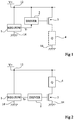
- the figure 1 shows schematically and in block form an example of application of a charge pump circuit 1 (NEG POW) for generating a negative voltage V- from a positive voltage V +.
- the negative voltage V- is used to supply a control circuit 2 (DRIVER) of a transistor 3 (typically a MOS transistor) in series with a load 4 (Q) between the application terminals 12.
- a positive potential V + and 14 for example of mass or corresponding to the high point of the load.
- the voltages involved at the level of the load 4 and the switching thresholds of the transistor 3 make it necessary to have a negative potential V- in order to correctly control the transistor 3.
- the figure 2 represents, schematically and in block form, another example of application of a circuit for generating a negative voltage V-.
- the voltage V- is, again, supplied to a control circuit 2 of a power transistor 3, connected in series with a load 4 (Q) supplied with a positive voltage.
- the transistor 3 is here connected on the ground side. Again, depending on the voltages involved and the switching thresholds of the transistor 3, it may be necessary to have a negative potential to control it properly.
- the negative voltage can be used to block a switch (transistor 3) having a closed-off state ("normally-on").
- a switch transistor 3
- a closed-off state normally-on
- Another example is the control of a power transistor having a threshold voltage close to zero and which requires a polarization of its control terminal with a negative voltage to move away from its threshold voltage and to prevent stray voltages from changing the blocked or passing state.
- Another example is the control of an IGBT transistor that sometimes uses a negative voltage to provide effective blocking.
- the figure 3 represents an example of a circuit diagram of an embodiment of a circuit 1 for generating a negative voltage, based on a capacitive charge pump.
- a transistor M1 typically a normally closed MOS transistor (normally on), is connected, directly or via a resistive element R (shown in dashed lines), to a terminal 12 for applying a potential V + positive with respect to to ground (terminal 14).
- the other power terminal of the transistor M1 is connected to a node 16 via a first capacitive element C1 and, at the terminal 14, by a first switch K1.
- the control terminal (the gate) of the transistor M1 is connected (connected directly) to the node 16.
- the node 16 is connected, by a second switch K2, to a terminal 18 for supplying the negative output voltage V-and, by a third switch K3 at the terminal 14 for applying the reference potential.
- Terminal 18 is also connected to the terminal 14 by a second capacitive element C2.
- the switches K1, K2 are controlled in all or nothing by a signal CT1.
- the switch K3 is controlled in all or nothing by a signal CT3.
- the figure 4 illustrates, in the form of chronograms, the operation of the circuit 1 of the figure 3 .
- timing diagrams respectively represent examples of the appearance of the signal CT2, conditioning the open or closed state of the switch K3, the voltage V15 of the node 15 between the transistor M1 and the capacitor C1, of the signal CT1, conditioning the state open or closed switches K1 and K2, the voltage V16 of the node 16, and the output voltage V-.
- switches K1, K2, K3 consisting of N-channel MOS transistors, and threshold voltages
- these transistors are turned on when their gates are connected to a positive potential (high states of the signals CT1 and CT2). and are blocked when their gates are connected to the ground (low states of the signals CT1 and CT2).
- a charge pump cycle begins at a time t0 at which the switch K3 is closed (high signal CT2), the switches K1 and K2 being open (signal CT1 in the low state).
- Node 15 starts grounded. Since the transistor M1 is normally on, the potential of the node 15 increases until a time t1 when the voltage V15 reaches the threshold voltage VT of the transistor M1. This amounts to charging the capacitor C1 to the blocking voltage (threshold voltage VT) of the transistor M1.
- a reverse switching phase is started, that is to say that the switches K1 and K2 are opened (signal CT1 at the low state), then at a posterior moment, corresponding to the start time t0 of a following cycle, switch K3 is closed.
- the minimum value (the most negative) that can take voltage V- is -VT.
- this -VT value is reached in one or more cycles. In the example of the figure 4 it is assumed that two cycles are necessary.
- the duration of the phase or phases T1, between times t0 and t2, is chosen to be greater than the time required to charge the capacitor C1 at the VT level. This duration is a function, in particular, of the capacity of the capacitor C1 and the drain-source resistance in the on state of the transistor M1.
- the duration of the phase or phases T2, between times t3 and t4, is chosen to be greater than the recharge time of the capacitor C1 through the transistor M1.
- T1 and T2 times are not necessarily the same. For example, a shorter T2 period, especially at startup, limits current calls.
- intervals Ta between the instants t2 and t3, and Tb between the instants t2 and t3, are chosen to guarantee a lack of simultaneous conduction of the switches K1 to K3.
- the polarization of the transistor M1 makes it possible to make it normally closed, which avoids a starting circuit.
- the optional resistive element R serves to limit the current calls.
- An advantage of the circuit described in relation to the Figures 3 and 4 is that it is compatible with an embodiment using only N-channel MOS transistors.
- Switchable transistor M1 power circuit switched capacity saves a start circuit.
- one of the switches used to switch the capacitive elements to switch this power transistor is used.
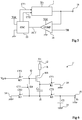
- the figure 5 represents, in simplified form and in block form, an example of a circuit for generating the control signals CT1 and CT2.
- an oscillator 22 controlled (activated) by a signal ACT supplied by a comparator 24 (COMP) between the level of the output voltage V- and a threshold TH is used.
- the TH threshold corresponds to a level above the -VT level to ensure the stop of the oscillator and thus reduce the consumption.
- the oscillator 22 and the comparator 24 are fed, for example, by a positive voltage Vdd, not necessarily identical to the voltage V +.
- a mono-pulse generator is used, triggered when the voltage V- has not reached a setpoint TH.
- an analog regulation which monitors the voltage across the capacitive element C1 and its discharge in the capacitive element C2.
- any circuit adapted to generate control signals to comply with the switching phases described above can be used.
- the figure 6 represents another embodiment for providing an output voltage V- less than -VT (greater, in absolute value, than the absolute value of the threshold voltage of the transistor M1).
- the gate of the transistor M1 is furthermore connected, via a switch K4 controlled by the signal CT1, to the node 16 and, via a switch K5 controlled by the signal CT2, to a potential of bias Vg greater than the reference potential (and lower than the potential V +).
- the switches K4 and K5 are preferably NMOS transistors.
- the switch K4 is open and the switch K5 is closed.
- the inversion of the voltage generated by the capacitive switching causes the voltage V- to reach -Vg-VT.
- Generating the potential Vg from the voltage V + does not pose a problem (for example a resistive bridge, preferably switchable to avoid permanent consumption, or a voltage regulator).
- the figure 7 represents another embodiment for achieving a more negative voltage than -VT.
- a second MOS transistor M2 optionally connected in series with a resistive element R1, the terminal 12 to the gate of the transistor M1, now connected to the node 16 by a resistive element R2 (or capacitive to reduce continuous consumption (dc)).
- the gate of transistor M2 is connected to node 16.
- the element C1 is charged to a value corresponding to the sum of the two threshold voltages of the transistors M1 and M2 and the negative voltage generated has in absolute value this value.
- the embodiment of the figure 7 can be extended to even lower negative voltages by adding other transistors based on the same mounting (between the gate of transistor M2 and node 16).
- time intervals Ta and Tb between the periods T1 and T2 of the charge pump circuit can be adapted to the necessary switching times of the different transistors.
- the negative voltage generated can be used to control any type of transistor (IGBT, JFET, etc.) and, more generally, to supply any type of circuit. requiring a negative voltage.
- the dimensioning of the capacitive elements C1 and C2, made if necessary in the form of several capacitors in parallel, depends on the application and in particular on the expected consumption of the element or elements connected to the terminal 18.
Landscapes
- Engineering & Computer Science (AREA)
- Power Engineering (AREA)
- Dc-Dc Converters (AREA)
- Electronic Switches (AREA)
- Semiconductor Integrated Circuits (AREA)
Claims (12)
- Eine Schaltung zur Erzeugung einer negativen Spannung (V-) aus einer positiven Spannung (V+), wobei folgendes vorgesehen ist:mindestens ein erster Transistor (M1) zwischen einem ersten Anschluss (12) zum Anlegen eines Potentials höher als ein Bezugs- bzw. Referenzpotential und einem ersten Knoten (15);ein erstes kapazitives Element (C1) zwischen dem ersten Knoten (15) und einem zweiten Knoten (16), wobei ein Steueranschluss des erwähnten ersten Transistors mit dem zweiten Knoten (16) verbunden ist;ein erster Schalter (K1) zwischen dem ersten Knoten (15) und einem zweiten Anschluss (14) zum Anlegen eines Bezugspotenzials;ein zweiter Schalter (K2) zwischen dem zweiten Knoten (16) und einem dritten Anschluss (18) zur Lieferung der erwähnten negativen Spannung;ein dritter Schalter (K3) zwischen dem zweiten Knoten (16) und dem zweiten Anschluss (14); undein zweites kapazitives Element (C2) zwischen dem dritten Anschluss (18) und dem zweiten Anschluss.
- Die Schaltung nach Anspruch 1, wobei ferner folgendes vorgesehen ist:ein erstes Widerstandselement (R) zwischen dem ersten Anschluss (12) und dem ersten Transistor (M1).
- Die Schaltung nach Anspruch 1 oder 2, wobei ferner folgendes vorgesehen ist:ein vierter Schalter (K4) zwischen dem Steueranschluss des ersten Transistors (M1) und dem zweiten Knoten (16); undein fünfter Schalter (K5) zwischen dem Steueranschluss des ersten Transistors (M1) und einem vierten Anschluss (22) zum Anlegen eines Potentials (Vg) höher als das Referenzpotential.
- Die Schaltung nach Anspruch 1 oder 2, wobei ferner folgendes vorgesehen ist:mindestens ein zweiter Transistor (M2) zwischen dem ersten Anschluss (12) und dem Steueranschluss des ersten Transistors (M1), wobei der Steueranschluss des zweiten Transistors mit dem zweiten Knoten (16) verbunden ist; undein zweites Widerstandselement (R2) angeordnet zwischen dem Steueranschluss des ersten Transistors und dem zweiten Knoten.
- Die Schaltung nach Anspruch 4, die ferner ein drittes Widerstandselement (R1) zwischen dem zweiten Transistor (M2) und dem ersten Anschluss (12) aufweist.
- Die Schaltung nach einem der Ansprüche 1 bis 5, wobei der Transistor bzw. die Transistoren (M1, M2) N-Kanal-Transistoren sind.
- Die Schaltung nach einem der Ansprüche 1 bis 6, wobei alle Schalter (K1, K2, K3, K4, K5) N-Kanal-MOS-Transistoren sind.
- Ein Verfahren zur Steuerung einer Schaltung nach einem der Ansprüche 1 bis 7, wobei:in einer ersten Phase (T1) die ersten und zweiten Schalter (K1, K2) ausgeschaltet sind, während der dritte Schalter (K3) eingeschaltet ist; undwobei in einer zweiten Phase (T2) die ersten und zweiten Schalter (K1, K2) eingeschaltet sind, während der dritte Schalter (K3) ausgeschaltet ist.
- Das Verfahren nach Anspruch 8, wobei die ersten und zweiten Phasen (T1, T2) wiederholt werden.
- Das Verfahren nach Anspruch 8 oder 9, wobei Intervalle (Ta, Tb) mit Zeitdauern kürzer als denen der ersten und zweiten Phasen (T1, T2) zwischen den aufeinanderfolgenden Phasen angeordnet sind und wobei alle Schalter (K1, K2, K3, K4, K5) abgeschaltet sind.
- Das Verfahren nach einem der Ansprüche 8 bis 10 bei Abhängigkeit von Anspruch 3, wobei:während der ersten Phase(n) (T1) der vierte Schalter (K4) ausgeschaltet ist und der fünfte Schalter (K5) eingeschaltet ist; und wobeiwährend der zweiten Phase(n) (T2) der vierte Schalter (K4) eingeschaltet ist und der fünfte Schalter (K5) ausgeschaltet ist.
- Eine elektronische Schaltung, die mindestens eine Schaltung nach irgendeinem der Ansprüche 1 bis 7 aufweist.
Applications Claiming Priority (2)
| Application Number | Priority Date | Filing Date | Title |
|---|---|---|---|
| FR1359117A FR3011146B1 (fr) | 2013-09-23 | 2013-09-23 | Circuit de pompe de charge de generation d'une tension negative |
| PCT/FR2014/052334 WO2015040336A2 (fr) | 2013-09-23 | 2014-09-19 | Circuit de pompe de charge de generation d'une tension negative |
Publications (2)
| Publication Number | Publication Date |
|---|---|
| EP3050187A2 EP3050187A2 (de) | 2016-08-03 |
| EP3050187B1 true EP3050187B1 (de) | 2017-06-21 |
Family
ID=49911655
Family Applications (1)
| Application Number | Title | Priority Date | Filing Date |
|---|---|---|---|
| EP14784312.2A Not-in-force EP3050187B1 (de) | 2013-09-23 | 2014-09-19 | Ladungspumpenschaltung zur erzeugung einer negativen spannung |
Country Status (4)
| Country | Link |
|---|---|
| US (1) | US9647537B2 (de) |
| EP (1) | EP3050187B1 (de) |
| FR (1) | FR3011146B1 (de) |
| WO (1) | WO2015040336A2 (de) |
Families Citing this family (2)
| Publication number | Priority date | Publication date | Assignee | Title |
|---|---|---|---|---|
| US12306256B2 (en) | 2022-07-07 | 2025-05-20 | Caterpillar Inc. | Sensor with self supplied negative rail for battery pack measurement |
| US20250125720A1 (en) * | 2023-10-11 | 2025-04-17 | Texas Instruments Incorporated | Circuit for output current regulation |
Family Cites Families (14)
| Publication number | Priority date | Publication date | Assignee | Title |
|---|---|---|---|---|
| US4679134A (en) * | 1985-10-01 | 1987-07-07 | Maxim Integrated Products, Inc. | Integrated dual charge pump power supply and RS-232 transmitter/receiver |
| EP0855788B1 (de) * | 1997-01-23 | 2005-06-22 | STMicroelectronics S.r.l. | NMOS, negative Ladungspumpe |
| US6021056A (en) * | 1998-12-14 | 2000-02-01 | The Whitaker Corporation | Inverting charge pump |
| EP1271440B1 (de) | 2001-06-25 | 2005-11-30 | EM Microelectronic-Marin SA | Hochspannungsregler mit externer Steuerung |
| US6674317B1 (en) * | 2002-09-18 | 2004-01-06 | Taiwan Semiconductor Manufacturing Company | Output stage of a charge pump circuit providing relatively stable output voltage without voltage degradation |
| ITTO20020821A1 (it) * | 2002-09-20 | 2004-03-21 | Atmel Corp | Pompa di carica negativa con polarizzazione di massa. |
| TWI293828B (en) * | 2005-04-28 | 2008-02-21 | Novatek Microelectronics Corp | Charge pump |
| EP1791245A1 (de) * | 2005-11-25 | 2007-05-30 | STMicroelectronics S.r.l. | Ladungspumpenschaltung |
| US8054054B2 (en) | 2006-01-27 | 2011-11-08 | International Rectifier Corporation | High voltage gate driver IC (HVIC) with internal charge pumping voltage source |
| GB2447426B (en) * | 2006-12-22 | 2011-07-13 | Wolfson Microelectronics Plc | Charge pump circuit and methods of operation thereof |
| DE102007020999A1 (de) * | 2007-05-04 | 2008-11-13 | Texas Instruments Deutschland Gmbh | Ladungspumpe zur Erzeugung einer Eingangsspannung für einen Operationsverstärker |
| US9111601B2 (en) * | 2012-06-08 | 2015-08-18 | Qualcomm Incorporated | Negative voltage generators |
| US9312755B2 (en) * | 2013-03-05 | 2016-04-12 | Qualcomm Incorporated | Charge pump power savings |
| CN103280967B (zh) * | 2013-05-29 | 2016-11-16 | 成都芯源系统有限公司 | 一种电荷泵及其使其负输出电压跟随正输出电压的方法 |
-
2013
- 2013-09-23 FR FR1359117A patent/FR3011146B1/fr not_active Expired - Fee Related
-
2014
- 2014-09-19 US US14/917,538 patent/US9647537B2/en not_active Expired - Fee Related
- 2014-09-19 EP EP14784312.2A patent/EP3050187B1/de not_active Not-in-force
- 2014-09-19 WO PCT/FR2014/052334 patent/WO2015040336A2/fr not_active Ceased
Non-Patent Citations (1)
| Title |
|---|
| None * |
Also Published As
| Publication number | Publication date |
|---|---|
| WO2015040336A3 (fr) | 2015-06-18 |
| FR3011146A1 (fr) | 2015-03-27 |
| EP3050187A2 (de) | 2016-08-03 |
| FR3011146B1 (fr) | 2015-10-23 |
| US9647537B2 (en) | 2017-05-09 |
| US20160226376A1 (en) | 2016-08-04 |
| WO2015040336A2 (fr) | 2015-03-26 |
Similar Documents
| Publication | Publication Date | Title |
|---|---|---|
| EP2882087B1 (de) | Gleichstrom-Gleichstrom-Wandler in diskontinuierlichem Betriebsmodus | |
| FR3013916A1 (fr) | Circuit de commande pour convertisseur de puissance | |
| EP2278696A1 (de) | Hochsetz und Umrichtspannungswandler und Betriebsverfahren dafür. | |
| EP3945673B1 (de) | Spannungsvergleicher | |
| FR3102900A1 (fr) | Convertisseur de tension | |
| EP1704634A1 (de) | Steuerung eines kurzschlusses in einer induktivität eines aufwaertswandlers | |
| WO2020002821A1 (fr) | Commande cyclique de cellules d'un circuit integre | |
| EP2932588B1 (de) | Schaltung zum vergleichen einer spannung mit einem schwellenwert und umwandlung von elektrischer energie | |
| EP3945674A1 (de) | Spannungswandler | |
| EP3267583A1 (de) | Auswahlschaltkreis einer betriebsspannung mit kontolliertem übergang | |
| EP3050187A2 (de) | Ladungspumpenschaltung zur erzeugung einer negativen spannung | |
| EP4037174B1 (de) | Synchronisierung einer elektronischen vorrichtung | |
| EP3087647B1 (de) | Leistungsregler mit linearer steuerung von stromspitzenbegrenzung und mit kurzschlussschutz | |
| FR2969417A1 (fr) | Alimentation capacitive a limitation de courant d'appel | |
| FR3029713A1 (fr) | Convertisseur continu-continu a demarrage a froid | |
| FR2971379A1 (fr) | Commande a hysteresis d'un dispositif electronique par un signal module en largeur d'impulsion | |
| WO2020011768A1 (fr) | Procede de declenchement de la mise a l'etat passant d'un transistor | |
| EP3726731B1 (de) | Steuerschaltkreis von transistoren | |
| EP3584918B1 (de) | Schaltwandler | |
| EP4346077B1 (de) | Transistorsteuerung | |
| EP3651363A1 (de) | Adiabatische logische zelle | |
| EP3020109B1 (de) | System zur stabilisierung der versorgungsspannung eines bordnetzes für ein kraftfahrzeug | |
| EP1710913B1 (de) | Getakte Stromversorgung | |
| EP1124314B1 (de) | Ladungspumpenvorrichtung | |
| EP3185389B1 (de) | Vorrichtung und elektrisches gerät zur erzeugung einer elektrischen spannung für eine informationsbearbeitungseinheit, und entsprechendes elektronisches system zur informationsbearbeitung |
Legal Events
| Date | Code | Title | Description |
|---|---|---|---|
| PUAI | Public reference made under article 153(3) epc to a published international application that has entered the european phase |
Free format text: ORIGINAL CODE: 0009012 |
|
| 17P | Request for examination filed |
Effective date: 20160307 |
|
| AK | Designated contracting states |
Kind code of ref document: A2 Designated state(s): AL AT BE BG CH CY CZ DE DK EE ES FI FR GB GR HR HU IE IS IT LI LT LU LV MC MK MT NL NO PL PT RO RS SE SI SK SM TR |
|
| AX | Request for extension of the european patent |
Extension state: BA ME |
|
| DAX | Request for extension of the european patent (deleted) | ||
| GRAP | Despatch of communication of intention to grant a patent |
Free format text: ORIGINAL CODE: EPIDOSNIGR1 |
|
| STAA | Information on the status of an ep patent application or granted ep patent |
Free format text: STATUS: GRANT OF PATENT IS INTENDED |
|
| INTG | Intention to grant announced |
Effective date: 20170202 |
|
| GRAS | Grant fee paid |
Free format text: ORIGINAL CODE: EPIDOSNIGR3 |
|
| GRAA | (expected) grant |
Free format text: ORIGINAL CODE: 0009210 |
|
| STAA | Information on the status of an ep patent application or granted ep patent |
Free format text: STATUS: THE PATENT HAS BEEN GRANTED |
|
| AK | Designated contracting states |
Kind code of ref document: B1 Designated state(s): AL AT BE BG CH CY CZ DE DK EE ES FI FR GB GR HR HU IE IS IT LI LT LU LV MC MK MT NL NO PL PT RO RS SE SI SK SM TR |
|
| REG | Reference to a national code |
Ref country code: GB Ref legal event code: FG4D Free format text: NOT ENGLISH |
|
| REG | Reference to a national code |
Ref country code: CH Ref legal event code: EP |
|
| REG | Reference to a national code |
Ref country code: IE Ref legal event code: FG4D Free format text: LANGUAGE OF EP DOCUMENT: FRENCH |
|
| REG | Reference to a national code |
Ref country code: AT Ref legal event code: REF Ref document number: 903737 Country of ref document: AT Kind code of ref document: T Effective date: 20170715 |
|
| REG | Reference to a national code |
Ref country code: DE Ref legal event code: R096 Ref document number: 602014011075 Country of ref document: DE |
|
| REG | Reference to a national code |
Ref country code: FR Ref legal event code: PLFP Year of fee payment: 4 |
|
| REG | Reference to a national code |
Ref country code: NL Ref legal event code: MP Effective date: 20170621 |
|
| PG25 | Lapsed in a contracting state [announced via postgrant information from national office to epo] |
Ref country code: HR Free format text: LAPSE BECAUSE OF FAILURE TO SUBMIT A TRANSLATION OF THE DESCRIPTION OR TO PAY THE FEE WITHIN THE PRESCRIBED TIME-LIMIT Effective date: 20170621 Ref country code: NO Free format text: LAPSE BECAUSE OF FAILURE TO SUBMIT A TRANSLATION OF THE DESCRIPTION OR TO PAY THE FEE WITHIN THE PRESCRIBED TIME-LIMIT Effective date: 20170921 Ref country code: GR Free format text: LAPSE BECAUSE OF FAILURE TO SUBMIT A TRANSLATION OF THE DESCRIPTION OR TO PAY THE FEE WITHIN THE PRESCRIBED TIME-LIMIT Effective date: 20170922 Ref country code: FI Free format text: LAPSE BECAUSE OF FAILURE TO SUBMIT A TRANSLATION OF THE DESCRIPTION OR TO PAY THE FEE WITHIN THE PRESCRIBED TIME-LIMIT Effective date: 20170621 Ref country code: LT Free format text: LAPSE BECAUSE OF FAILURE TO SUBMIT A TRANSLATION OF THE DESCRIPTION OR TO PAY THE FEE WITHIN THE PRESCRIBED TIME-LIMIT Effective date: 20170621 |
|
| REG | Reference to a national code |
Ref country code: LT Ref legal event code: MG4D |
|
| REG | Reference to a national code |
Ref country code: AT Ref legal event code: MK05 Ref document number: 903737 Country of ref document: AT Kind code of ref document: T Effective date: 20170621 |
|
| PG25 | Lapsed in a contracting state [announced via postgrant information from national office to epo] |
Ref country code: RS Free format text: LAPSE BECAUSE OF FAILURE TO SUBMIT A TRANSLATION OF THE DESCRIPTION OR TO PAY THE FEE WITHIN THE PRESCRIBED TIME-LIMIT Effective date: 20170621 Ref country code: SE Free format text: LAPSE BECAUSE OF FAILURE TO SUBMIT A TRANSLATION OF THE DESCRIPTION OR TO PAY THE FEE WITHIN THE PRESCRIBED TIME-LIMIT Effective date: 20170621 Ref country code: NL Free format text: LAPSE BECAUSE OF FAILURE TO SUBMIT A TRANSLATION OF THE DESCRIPTION OR TO PAY THE FEE WITHIN THE PRESCRIBED TIME-LIMIT Effective date: 20170621 Ref country code: LV Free format text: LAPSE BECAUSE OF FAILURE TO SUBMIT A TRANSLATION OF THE DESCRIPTION OR TO PAY THE FEE WITHIN THE PRESCRIBED TIME-LIMIT Effective date: 20170621 Ref country code: BG Free format text: LAPSE BECAUSE OF FAILURE TO SUBMIT A TRANSLATION OF THE DESCRIPTION OR TO PAY THE FEE WITHIN THE PRESCRIBED TIME-LIMIT Effective date: 20170921 |
|
| PG25 | Lapsed in a contracting state [announced via postgrant information from national office to epo] |
Ref country code: CZ Free format text: LAPSE BECAUSE OF FAILURE TO SUBMIT A TRANSLATION OF THE DESCRIPTION OR TO PAY THE FEE WITHIN THE PRESCRIBED TIME-LIMIT Effective date: 20170621 Ref country code: RO Free format text: LAPSE BECAUSE OF FAILURE TO SUBMIT A TRANSLATION OF THE DESCRIPTION OR TO PAY THE FEE WITHIN THE PRESCRIBED TIME-LIMIT Effective date: 20170621 Ref country code: SK Free format text: LAPSE BECAUSE OF FAILURE TO SUBMIT A TRANSLATION OF THE DESCRIPTION OR TO PAY THE FEE WITHIN THE PRESCRIBED TIME-LIMIT Effective date: 20170621 Ref country code: AT Free format text: LAPSE BECAUSE OF FAILURE TO SUBMIT A TRANSLATION OF THE DESCRIPTION OR TO PAY THE FEE WITHIN THE PRESCRIBED TIME-LIMIT Effective date: 20170621 Ref country code: EE Free format text: LAPSE BECAUSE OF FAILURE TO SUBMIT A TRANSLATION OF THE DESCRIPTION OR TO PAY THE FEE WITHIN THE PRESCRIBED TIME-LIMIT Effective date: 20170621 |
|
| PG25 | Lapsed in a contracting state [announced via postgrant information from national office to epo] |
Ref country code: IT Free format text: LAPSE BECAUSE OF FAILURE TO SUBMIT A TRANSLATION OF THE DESCRIPTION OR TO PAY THE FEE WITHIN THE PRESCRIBED TIME-LIMIT Effective date: 20170621 Ref country code: SM Free format text: LAPSE BECAUSE OF FAILURE TO SUBMIT A TRANSLATION OF THE DESCRIPTION OR TO PAY THE FEE WITHIN THE PRESCRIBED TIME-LIMIT Effective date: 20170621 Ref country code: IS Free format text: LAPSE BECAUSE OF FAILURE TO SUBMIT A TRANSLATION OF THE DESCRIPTION OR TO PAY THE FEE WITHIN THE PRESCRIBED TIME-LIMIT Effective date: 20171021 Ref country code: ES Free format text: LAPSE BECAUSE OF FAILURE TO SUBMIT A TRANSLATION OF THE DESCRIPTION OR TO PAY THE FEE WITHIN THE PRESCRIBED TIME-LIMIT Effective date: 20170621 Ref country code: PL Free format text: LAPSE BECAUSE OF FAILURE TO SUBMIT A TRANSLATION OF THE DESCRIPTION OR TO PAY THE FEE WITHIN THE PRESCRIBED TIME-LIMIT Effective date: 20170621 |
|
| REG | Reference to a national code |
Ref country code: DE Ref legal event code: R097 Ref document number: 602014011075 Country of ref document: DE |
|
| PLBE | No opposition filed within time limit |
Free format text: ORIGINAL CODE: 0009261 |
|
| STAA | Information on the status of an ep patent application or granted ep patent |
Free format text: STATUS: NO OPPOSITION FILED WITHIN TIME LIMIT |
|
| PG25 | Lapsed in a contracting state [announced via postgrant information from national office to epo] |
Ref country code: DK Free format text: LAPSE BECAUSE OF FAILURE TO SUBMIT A TRANSLATION OF THE DESCRIPTION OR TO PAY THE FEE WITHIN THE PRESCRIBED TIME-LIMIT Effective date: 20170621 |
|
| REG | Reference to a national code |
Ref country code: CH Ref legal event code: PL |
|
| 26N | No opposition filed |
Effective date: 20180322 |
|
| PG25 | Lapsed in a contracting state [announced via postgrant information from national office to epo] |
Ref country code: MC Free format text: LAPSE BECAUSE OF FAILURE TO SUBMIT A TRANSLATION OF THE DESCRIPTION OR TO PAY THE FEE WITHIN THE PRESCRIBED TIME-LIMIT Effective date: 20170621 |
|
| REG | Reference to a national code |
Ref country code: IE Ref legal event code: MM4A |
|
| REG | Reference to a national code |
Ref country code: BE Ref legal event code: MM Effective date: 20170930 |
|
| PG25 | Lapsed in a contracting state [announced via postgrant information from national office to epo] |
Ref country code: LU Free format text: LAPSE BECAUSE OF NON-PAYMENT OF DUE FEES Effective date: 20170919 |
|
| PG25 | Lapsed in a contracting state [announced via postgrant information from national office to epo] |
Ref country code: IE Free format text: LAPSE BECAUSE OF NON-PAYMENT OF DUE FEES Effective date: 20170919 Ref country code: CH Free format text: LAPSE BECAUSE OF NON-PAYMENT OF DUE FEES Effective date: 20170930 Ref country code: LI Free format text: LAPSE BECAUSE OF NON-PAYMENT OF DUE FEES Effective date: 20170930 |
|
| PG25 | Lapsed in a contracting state [announced via postgrant information from national office to epo] |
Ref country code: BE Free format text: LAPSE BECAUSE OF NON-PAYMENT OF DUE FEES Effective date: 20170930 Ref country code: SI Free format text: LAPSE BECAUSE OF FAILURE TO SUBMIT A TRANSLATION OF THE DESCRIPTION OR TO PAY THE FEE WITHIN THE PRESCRIBED TIME-LIMIT Effective date: 20170621 |
|
| PG25 | Lapsed in a contracting state [announced via postgrant information from national office to epo] |
Ref country code: MT Free format text: LAPSE BECAUSE OF FAILURE TO SUBMIT A TRANSLATION OF THE DESCRIPTION OR TO PAY THE FEE WITHIN THE PRESCRIBED TIME-LIMIT Effective date: 20170621 |
|
| REG | Reference to a national code |
Ref country code: FR Ref legal event code: PLFP Year of fee payment: 5 |
|
| GBPC | Gb: european patent ceased through non-payment of renewal fee |
Effective date: 20180919 |
|
| PG25 | Lapsed in a contracting state [announced via postgrant information from national office to epo] |
Ref country code: HU Free format text: LAPSE BECAUSE OF FAILURE TO SUBMIT A TRANSLATION OF THE DESCRIPTION OR TO PAY THE FEE WITHIN THE PRESCRIBED TIME-LIMIT; INVALID AB INITIO Effective date: 20140919 |
|
| PG25 | Lapsed in a contracting state [announced via postgrant information from national office to epo] |
Ref country code: GB Free format text: LAPSE BECAUSE OF NON-PAYMENT OF DUE FEES Effective date: 20180919 Ref country code: CY Free format text: LAPSE BECAUSE OF FAILURE TO SUBMIT A TRANSLATION OF THE DESCRIPTION OR TO PAY THE FEE WITHIN THE PRESCRIBED TIME-LIMIT Effective date: 20170621 |
|
| PG25 | Lapsed in a contracting state [announced via postgrant information from national office to epo] |
Ref country code: MK Free format text: LAPSE BECAUSE OF FAILURE TO SUBMIT A TRANSLATION OF THE DESCRIPTION OR TO PAY THE FEE WITHIN THE PRESCRIBED TIME-LIMIT Effective date: 20170621 |
|
| PG25 | Lapsed in a contracting state [announced via postgrant information from national office to epo] |
Ref country code: TR Free format text: LAPSE BECAUSE OF FAILURE TO SUBMIT A TRANSLATION OF THE DESCRIPTION OR TO PAY THE FEE WITHIN THE PRESCRIBED TIME-LIMIT Effective date: 20170621 |
|
| PG25 | Lapsed in a contracting state [announced via postgrant information from national office to epo] |
Ref country code: PT Free format text: LAPSE BECAUSE OF FAILURE TO SUBMIT A TRANSLATION OF THE DESCRIPTION OR TO PAY THE FEE WITHIN THE PRESCRIBED TIME-LIMIT Effective date: 20170621 |
|
| PG25 | Lapsed in a contracting state [announced via postgrant information from national office to epo] |
Ref country code: AL Free format text: LAPSE BECAUSE OF FAILURE TO SUBMIT A TRANSLATION OF THE DESCRIPTION OR TO PAY THE FEE WITHIN THE PRESCRIBED TIME-LIMIT Effective date: 20170621 |
|
| PGFP | Annual fee paid to national office [announced via postgrant information from national office to epo] |
Ref country code: FR Payment date: 20200930 Year of fee payment: 7 Ref country code: DE Payment date: 20200910 Year of fee payment: 7 |
|
| REG | Reference to a national code |
Ref country code: DE Ref legal event code: R119 Ref document number: 602014011075 Country of ref document: DE |
|
| PG25 | Lapsed in a contracting state [announced via postgrant information from national office to epo] |
Ref country code: FR Free format text: LAPSE BECAUSE OF NON-PAYMENT OF DUE FEES Effective date: 20210930 Ref country code: DE Free format text: LAPSE BECAUSE OF NON-PAYMENT OF DUE FEES Effective date: 20220401 |