EP3043283B1 - Device and method for generating identification key - Google Patents
Device and method for generating identification key Download PDFInfo
- Publication number
- EP3043283B1 EP3043283B1 EP14842135.7A EP14842135A EP3043283B1 EP 3043283 B1 EP3043283 B1 EP 3043283B1 EP 14842135 A EP14842135 A EP 14842135A EP 3043283 B1 EP3043283 B1 EP 3043283B1
- Authority
- EP
- European Patent Office
- Prior art keywords
- region
- bjt
- threshold
- width
- shorted
- Prior art date
- Legal status (The legal status is an assumption and is not a legal conclusion. Google has not performed a legal analysis and makes no representation as to the accuracy of the status listed.)
- Active
Links
- 238000000034 method Methods 0.000 title claims description 66
- 230000003071 parasitic effect Effects 0.000 claims description 30
- 238000004519 manufacturing process Methods 0.000 claims description 19
- 239000004065 semiconductor Substances 0.000 claims description 14
- 230000000295 complement effect Effects 0.000 claims description 4
- 229910044991 metal oxide Inorganic materials 0.000 claims description 4
- 150000004706 metal oxides Chemical class 0.000 claims description 4
- 239000000758 substrate Substances 0.000 description 11
- 238000012938 design process Methods 0.000 description 6
- 238000010586 diagram Methods 0.000 description 6
- 230000005669 field effect Effects 0.000 description 4
- 230000007423 decrease Effects 0.000 description 3
- 239000000463 material Substances 0.000 description 2
- 230000015572 biosynthetic process Effects 0.000 description 1
- 230000002950 deficient Effects 0.000 description 1
- 239000011229 interlayer Substances 0.000 description 1
- 239000010410 layer Substances 0.000 description 1
Images


Classifications
-
- G—PHYSICS
- G06—COMPUTING; CALCULATING OR COUNTING
- G06F—ELECTRIC DIGITAL DATA PROCESSING
- G06F21/00—Security arrangements for protecting computers, components thereof, programs or data against unauthorised activity
- G06F21/60—Protecting data
-
- H—ELECTRICITY
- H01—ELECTRIC ELEMENTS
- H01L—SEMICONDUCTOR DEVICES NOT COVERED BY CLASS H10
- H01L23/00—Details of semiconductor or other solid state devices
- H01L23/57—Protection from inspection, reverse engineering or tampering
- H01L23/576—Protection from inspection, reverse engineering or tampering using active circuits
-
- G—PHYSICS
- G06—COMPUTING; CALCULATING OR COUNTING
- G06F—ELECTRIC DIGITAL DATA PROCESSING
- G06F21/00—Security arrangements for protecting computers, components thereof, programs or data against unauthorised activity
- G06F21/70—Protecting specific internal or peripheral components, in which the protection of a component leads to protection of the entire computer
- G06F21/71—Protecting specific internal or peripheral components, in which the protection of a component leads to protection of the entire computer to assure secure computing or processing of information
- G06F21/73—Protecting specific internal or peripheral components, in which the protection of a component leads to protection of the entire computer to assure secure computing or processing of information by creating or determining hardware identification, e.g. serial numbers
-
- G—PHYSICS
- G09—EDUCATION; CRYPTOGRAPHY; DISPLAY; ADVERTISING; SEALS
- G09C—CIPHERING OR DECIPHERING APPARATUS FOR CRYPTOGRAPHIC OR OTHER PURPOSES INVOLVING THE NEED FOR SECRECY
- G09C1/00—Apparatus or methods whereby a given sequence of signs, e.g. an intelligible text, is transformed into an unintelligible sequence of signs by transposing the signs or groups of signs or by replacing them by others according to a predetermined system
-
- H—ELECTRICITY
- H01—ELECTRIC ELEMENTS
- H01L—SEMICONDUCTOR DEVICES NOT COVERED BY CLASS H10
- H01L27/00—Devices consisting of a plurality of semiconductor or other solid-state components formed in or on a common substrate
- H01L27/02—Devices consisting of a plurality of semiconductor or other solid-state components formed in or on a common substrate including semiconductor components specially adapted for rectifying, oscillating, amplifying or switching and having at least one potential-jump barrier or surface barrier; including integrated passive circuit elements with at least one potential-jump barrier or surface barrier
- H01L27/0203—Particular design considerations for integrated circuits
- H01L27/0207—Geometrical layout of the components, e.g. computer aided design; custom LSI, semi-custom LSI, standard cell technique
-
- H—ELECTRICITY
- H04—ELECTRIC COMMUNICATION TECHNIQUE
- H04L—TRANSMISSION OF DIGITAL INFORMATION, e.g. TELEGRAPHIC COMMUNICATION
- H04L9/00—Cryptographic mechanisms or cryptographic arrangements for secret or secure communications; Network security protocols
- H04L9/08—Key distribution or management, e.g. generation, sharing or updating, of cryptographic keys or passwords
- H04L9/0861—Generation of secret information including derivation or calculation of cryptographic keys or passwords
- H04L9/0866—Generation of secret information including derivation or calculation of cryptographic keys or passwords involving user or device identifiers, e.g. serial number, physical or biometrical information, DNA, hand-signature or measurable physical characteristics
-
- H—ELECTRICITY
- H01—ELECTRIC ELEMENTS
- H01L—SEMICONDUCTOR DEVICES NOT COVERED BY CLASS H10
- H01L2924/00—Indexing scheme for arrangements or methods for connecting or disconnecting semiconductor or solid-state bodies as covered by H01L24/00
- H01L2924/0001—Technical content checked by a classifier
- H01L2924/0002—Not covered by any one of groups H01L24/00, H01L24/00 and H01L2224/00
-
- H—ELECTRICITY
- H04—ELECTRIC COMMUNICATION TECHNIQUE
- H04L—TRANSMISSION OF DIGITAL INFORMATION, e.g. TELEGRAPHIC COMMUNICATION
- H04L2209/00—Additional information or applications relating to cryptographic mechanisms or cryptographic arrangements for secret or secure communication H04L9/00
- H04L2209/12—Details relating to cryptographic hardware or logic circuitry
Definitions
- the following description relates to a device and method for generating an identification key for hardware security, and more particularly, to a device and method for generating an identification key by implementing a physically unclonable function (PUF) based on a semiconductor process variation.
- PAF physically unclonable function
- a PUF may provide an identification key, that is, an unpredictable digital value. Individual PUFs may provide different digital values, even though an accurate manufacturing process is provided and the individual PUFs are manufactured through the same design and manufacturing process.
- the PUF may be referred to as a "physical one-way function (POWF)" that is practically impossible to be duplicated.
- PWF physical one-way function
- the above characteristic of the PUF may be used to generate an identification key for security and/or authentication.
- the PUF may be used to provide a unique key to distinguish devices from one another.
- '630 patent discloses a method of probabilistically determining whether an inter-layer contact or a via is formed between conductive layers of a semiconductor based on a semiconductor process variation.
- US2011317829 describes basing a PUF on relative threshold voltages of a pair of field effect transistors. Each field effect transistor is connected in a circuit wherein its output voltage depends on its threshold voltages. A pair of the field effect transistors is selected and the outputs of the selected field effect transistors are coupled to a comparator. The comparator compares the output voltages and generates a response indicating which of the selected transistors has the higher output voltage.
- a device for generating an identification key including a bipolar junction transistor (BJT) having an effective base width equal to or greater than a first threshold and equal to or less than a second threshold, and a reader configured to determine whether an emitter region and a collector region of the BJT are shorted and to provide an identification key, when a base-emitter voltage of the BJT less than a predetermined potential difference is applied.
- BJT bipolar junction transistor
- the first threshold may be a lower limit value of a range of the effective base width to allow a difference between a probability that the emitter region and the collector region are shorted and a probability that the emitter region and the collector region are not shorted to be within a predetermined error range
- the second threshold may be an upper limit value of the range
- the BJT may be designed so that the effective base width may be less than a value specified in a design rule, may be equal to or greater than the first threshold and may be equal to or less than the second threshold.
- Whether the emitter region and the collector region are shorted may be randomly determined by a process variation in a manufacturing process of the BJT.
- the BJT may include a parasitic BJT formed by at least one N+ region and at least one P+ region in a complementary metal-oxide semiconductor (CMOS) process.
- CMOS complementary metal-oxide semiconductor
- a device for generating an identification key including a BJT in which a difference between a width of a base region and a sum of a width of a first depletion region and a width of a second depletion region is equal to or greater than a first threshold and equal to or less than a second threshold, the first depletion region being formed by a junction between an emitter region and the base region and the second depletion region being formed by a junction between a collector region and the base region, and a reader configured to determine whether the emitter region and the collector region of the BJT are shorted and to provide an identification key, when a base-emitter voltage of the BJT less than a predetermined potential difference is applied.
- the first threshold may be a lower limit value of a range of an effective base width to allow a difference between a probability that the emitter region and the collector region are shorted and a probability that the emitter region and the collector region are not shorted to be within a predetermined error range
- the second threshold may be an upper limit value of the range
- the BJT may be designed so that a width of the base region may be less than a value specified in a design rule and that the difference between the width of the base region and the sum of the width of the first depletion region and the width of the second depletion region may be equal to or greater than the first threshold and equal to or less than the second threshold.
- a method of generating an identification key including reading, by a reader, whether an emitter region and a collector region of a BJT are shorted in a state in which a base-emitter voltage of the BJT is maintained to be less than a predetermined potential difference, the BJT having an effective base width equal to or greater than a first threshold and equal to or less than a second threshold, and providing an identification key corresponding to the BJT based on a result of the reading.
- the first threshold may be a lower limit value of a range of the effective base width to allow a difference between a probability that the emitter region and the collector region are shorted and a probability that the emitter region and the collector region are not shorted to be within a predetermined error range
- the second threshold may be an upper limit value of the range
- the BJT may be designed so that the effective base width may be less than a value specified in a design rule and that the effective base width may be equal to or greater than the first threshold and equal to or less than the second threshold.
- Whether the emitter region and the collector region are shorted may be randomly determined by a process variation in a manufacturing process of the BJT.
- the BJT may include a parasitic BJT formed by at least one N+ region and at least one P+ region in a CMOS process.
- a method of manufacturing a device for generating an identification key including forming a BJT so that an effective base width is equal to or greater than a first threshold and equal to or less than a second threshold, and forming a reader configured to determine whether an emitter region and a collector region of the BJT are shorted and to provide an identification key, when a base-emitter voltage of the BJT less than a predetermined potential difference is applied.
- the first threshold may be a lower limit value of a range of the effective base width to allow a difference between a probability that the emitter region and the collector region are shorted and a probability that the emitter region and the collector region are not shorted to be within a predetermined error range
- the second threshold may be an upper limit value of the range
- the BJT may be designed so that the effective base width may be less than a value specified in a design rule, may be equal to or greater than the first threshold and may be equal to or less than the second threshold.
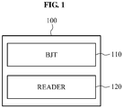
- FIG. 1 is a block diagram illustrating of a device 100 for generating an identification key according to an embodiment.
- the device 100 may include a bipolar junction transistor (BJT) 110 and a reader 120.
- An electrical characteristic of the BJT 110 may be determined by a process variation.
- the BJT 110 may include a collector region, a base region and an emitter region.
- a depletion region may be formed by a P-N junction between a collector region and a base region, and a depletion region may be formed by a P-N junction between the base region and an emitter region.
- a BJT may be designed so that the above depletion regions are included in a base region based on a process parameter, for example, semiconductor materials or a doping concentration.
- the BJT when a BJT is manufactured by applying a typical process parameter, and when a typical turn-on voltage is not supplied to a base region and an emitter region, the BJT may be turned off and a current may not flow between the emitter region and a collector region.
- the typical turn-on voltage may be understood as a bias voltage applied to the base region to turn on the BJT in an application according to a related art in which the BJT is used as a typical semiconductor transistor.
- the turn-on voltage of the BJT may be readily understood by one of ordinary skill in the art, and accordingly further description thereof is omitted.
- a BJT may be manufactured by applying different doping concentrations or different widths of a base region, instead of applying the typical process parameter, in a design process and/or a manufacturing process.
- a BJT may be manufactured so that an effective base width may be less than a typical value.
- the effective base width may refer to a width of a base region between a first depletion region and a second depletion region.
- the first depletion region may be formed by a junction between an emitter region and the base region, and the second depletion region may be formed by a junction between a collector region and the base region.
- a distance between the first depletion region and the second depletion region may decrease.
- the collector region and the emitter region may be shorted even though a voltage equal to or less than a typical turn-on voltage is applied between the base region and the emitter region.
- a current may flow due to punch-through.
- the effective base width may be determined based on a process parameter, and the like, and/or may be determined to be equal to or less than a found threshold.
- a process parameter and the like, and/or may be determined to be equal to or less than a found threshold.
- an emitter region and a collector region may be shorted and a current may be generated due to punch-through.
- an emitter region and a collector region may be open and the current may not be generated.
- a lower limit of the effective base width may guarantee that a short circuit between an emitter and a collector does not occur.
- an upper limit of the effective base width may guarantee that the short circuit between the emitter and the collector occurs. For example, when the effective base width is greater than the lower limit and less than the upper limit, the short circuit between the emitter and the collector may probabilistically occur.
- the first threshold and the second threshold may be set so that a probability of generation of a current by punch-through is closest to 50% by repeating a process of manufacturing and measuring various effective base widths to adjust the effective base width.
- the first threshold and the second threshold may be a lower limit value and an upper limit value, respectively, in a range of the effective base width in which a difference between a probability that a collector region and an emitter region are shorted and a probability that the collector region and the emitter region are not shorted is within a predetermined error range. Accordingly, the collector region and the emitter region may be manufactured so that whether the collector region and the emitter region are shorted may be randomly determined.
- a BJT may be manufactured so that a difference between a width of a base region and a sum of a width of a first depletion region formed by a junction between an emitter region and the base region and a width of a second depletion region formed by a junction between a collector region and the base region may be equal to or greater than a first threshold and equal to or less than a second threshold.
- the collector region and the emitter region may be randomly shorted and a current may flow.
- the BJT may be manufactured so that the difference between the width of the base region and the sum of the width of the first depletion region formed by the junction with the emitter region and the width of the second depletion region formed by the junction with the collector region may be equal to or greater than the first threshold and equal to or less than the second threshold.
- the above thresholds may be set to values allowing a difference between a probability that the collector region and the emitter region are shorted and a probability that the collector region and the emitter region are not shorted to be within a predetermined error range, and thus it is possible to further ensure randomness of whether the collector region and the emitter region are shorted.
- the collector region and the emitter region may be shorted and a current may flow at all times even though the BJT is turned off.
- a lower limit of the difference between the width of the base region and the sum of the width of the first depletion region and the width of the second depletion region may guarantee that a short circuit between an emitter and a collector does not occur.
- an upper limit of the difference between the width of the base region and the sum of the width of the first depletion region and the width of the second depletion region may guarantee that the short circuit between the emitter and the collector occurs.
- the difference between the width of the base region and the sum of the width of the first depletion region and the width of the second depletion region may be determined in a range of the difference between the width of the base region and the sum of the width of the first depletion region and the width of the second depletion region to allow a probability that a current is generated due to punch-through between a collector and an emitter to be about 50%, however, there is no limitation thereto.
- the first threshold and the second threshold may be set so that a probability of generation of a current by punch-through is closest to 50% by repeating a process of manufacturing and measuring various widths of the first depletion region and various widths of the second depletion region.
- the first threshold and the second threshold may be a lower limit value and an upper limit value, respectively, in a range of the effective base width in which a difference between a probability that a collector region and an emitter region are shorted and a probability that the collector region and the emitter region are not shorted is within a predetermined error range. Accordingly, the collector region and the emitter region may be manufactured so that whether the collector region and the emitter region are shorted may be randomly determined.
- the above result may be determined as a process failure.
- a collector region and an emitter region may be shorted by a designed effective base width or widths of depletion regions, and accordingly a semiconductor may be determined as a defective product.
- a physical unclonable function may be generated based on a result of the above random short circuit phenomenon.
- the above random process failure may be caused by formation of a channel between the collector region and the emitter region even though the BJT is not turned on while the distance between the first depletion region and the second depletion region decreases.
- the effective base width and/or the width of the first depletion region and the width of the second depletion region may be adjusted during a semiconductor design process.
- this is merely an example, and it is possible to create the same result through an operation in a semiconductor process even though a design corresponds to a typical BJT. Accordingly, even though a portion of a design or a manufacturing process is described hereinafter, there is no limitation to some embodiments by the above description.
- the collector region and the emitter region may be shorted.
- whether the collector region and the emitter region are shorted may not be predicted, which may guarantee randomness of a digital value generated by the PUF.
- a process error of a certain level may be inevitable. Also, because it is impossible to control a behavior and occurrence of the process error to be beyond a predetermined range, whether a collector region and an emitter region of each of manufactured BJTs may be determined for each of the BJTs.
- the BJT in a design and/or a manufacturing process of a BJT, may be formed by adjusting an effective base width and/or a width of a first depletion region and a width of a second depletion region based on a design rule that specifies a base width to guarantee that existing punch-through does not occur, and thus whether a collector region and an emitter region are shorted may be randomly determined.
- a design rule that specifies a base width to guarantee that existing punch-through does not occur, and thus whether a collector region and an emitter region are shorted may be randomly determined.
- the design rule may be a design rule that ensures that an emitter and a collector of a BJT are not shorted due to punch-through.
- the design rule will be understood as described above.
- adjustment of the effective base width, the width of the first depletion region and the width of the second depletion region is merely an example among BJT process parameters that may short the collector region and the emitter region. Accordingly, the adjustment should be understood to include an adjustment of an arbitrary BJT process parameter to short the collector region and the emitter region, and not limited to a portion of a configuration described as an example in the specification.
- the reader 120 may determine whether a collector region and an emitter region of a manufactured BJT are shorted, and may provide an identification key as an output value.
- a typical turn-off voltage may be applied to a base region and an emitter region, and the BJT may be typically turned off.
- the BJT may be turned off, whether a collector region and the emitter region are shorted may be determined based on an output value. Also, a value of "0" or "1" may be output as an output value, and an identification key may be provided.
- a voltage less than a predetermined potential difference may be applied between a base and an emitter of a manufactured BJT.
- the predetermined potential difference may be less than a typical turn-off voltage to turn off a BJT.
- the predetermined potential difference may be a low potential difference to turn off the BJT even though an effective base width of the BJT is equal to or greater than a first threshold and equal to or less than a second threshold.
- a predetermined potential difference between a base and an emitter may be "0" volts (V).
- FIG. 2 is a diagram provided to describe a concept of a configuration 200 of a BJT according to an embodiment.
- a first depletion region 210 may be formed by a junction between an emitter region and a base region
- a second depletion region 220 may be formed by a junction between a collector region and the base region.
- a distance between the first depletion region 210 and the second depletion region 220 may be represented as an effective base width W eff .
- the effective base width W eff may be designed to have a value equal to or greater than a typical value.
- a predetermined distance between the first depletion region 210 and the second depletion region 220 may be secured. Accordingly, when a typical turn-on voltage is not supplied between the base region and the emitter region, a channel may not be formed, and accordingly a current may not flow.
- a difference between a width W B of the base region and a sum of a width W BE of the first depletion region 210 and a width W BC of the second depletion region 220 may be designed to be greater than a typical value.
- a predetermined distance between the first depletion region 210 and the second depletion region 220 may be secured. Accordingly, when a typical turn-on voltage is not supplied between the base region and the emitter region, a channel may not be formed, and accordingly a current may not flow.
- the effective base width W eff may be equal to or greater than a first threshold and equal to or less than a second threshold.
- the emitter region and the collector region may be randomly shorted.
- a current may flow between the emitter region and the collector region, even though the typical turn-on voltage is not supplied between the base region and the emitter region.
- a voltage of the emitter region may be applied to a voltage of the collector region, and a reader may identify the voltage and may provide an identification key as an output value. Because whether the emitter region and the collector region are shorted is randomly determined, randomness of a digital value generated by a PUF may be guaranteed.
- the difference between the width W B of the base region and the sum of the width W BE of the first depletion region 210 and the width W BC of the second depletion region 220 may be designed to be equal to or greater than the first threshold and equal to or less than the second threshold.
- the emitter region and the collector region may be probabilistically shorted. When the emitter region and the collector region are shorted, a current may flow between the emitter region and the collector region, even though the typical turn-on voltage is not supplied between the base region and the emitter region.
- a voltage of the emitter region may be applied to a voltage of the collector region, and a reader may identify the voltage and provide an identification key as an output value. Because whether the emitter region and the collector region are shorted is randomly determined, randomness of a digital value generated by a PUF may be guaranteed.
- the above-described embodiments may be implemented by designing different process parameters in a design or by a process variation in a BJT manufacturing process. Also, whether the collector region and the emitter region are shorted may remain unchanged unless a separate BJT process is performed after a BJT is manufactured. Thus, time-invariance may also be guaranteed and the BJT may be used to generate a PUF.
- FIG. 3A is a diagram provided to describe a concept of an operation of a BJT based on a width of a base region and a width of a depletion region according to an embodiment.
- a width W B of a base region may be greater than a sum of a width W BE of a first depletion region and a width W BC of a second depletion region in the BJT 310.
- the BJT 310 when a typical turn-on voltage is not applied between the base region and an emitter region, the BJT 310 may be turned off. Accordingly, a current may not be generated between a collector region and the emitter region, and the collector region and the emitter region may be open.
- a difference between a width W B of a base region and a sum of a width W BE of a first depletion region and a width W BC of a second depletion region may be equal to or greater than a first threshold and equal to or less than a second threshold in the BJT 320.
- a difference between a probability that a collector region and an emitter region are shorted and a probability that the collector region and the emitter region are not shorted may be within a predetermined error range.
- the first threshold and the second threshold may be a lower limit value and an upper limit value, respectively, in a range of the effective base width in which a difference between a probability that a collector region and an emitter region are shorted and a probability that the collector region and the emitter region are not shorted is within a predetermined error range. Accordingly, whether the collector region and the emitter region are shorted may be randomly determined.
- the collector region and the emitter region may be shorted, and a current may be generated in the BJT due to punch-through.
- the collector region and the emitter region are not shorted, the current may not be generated.
- a voltage less than a predetermined potential difference may be applied between a base and an emitter of a manufactured BJT.
- the predetermined potential difference may be less than a typical turn-off voltage to turn off a BJT.
- the predetermined potential difference may be a low potential difference to turn off the BJT even though an effective base width of the BJT is equal to or greater than a first threshold and equal to or less than a second threshold.
- a predetermined potential difference between a base and an emitter may be "0" V.
- a width W B of a base region may be less than a sum of a width W BE of a first depletion region and a width W BC of a second depletion region.
- a collector region and the emitter region may be shorted and a current may be generated due to punch-through.
- a principle of an operation of shorting the collector region and the emitter region by adjusting an effective base width may be the same as that described above.
- An effective base width may refer to a distance between the first depletion region with the width W BE and the second depletion region with the width W BC .
- the effective base width is equal to or greater than a typical value, the same operation principle as that of the BJT 310 manufactured so that the width W B of the base region is greater than the sum of the width W BE of the first depletion region and the width W BC of the second depletion region may be provided.
- the same operation principle as that of the BJT 320 manufactured so that the difference between the width W B of the base region and the sum of the width W BE of the first depletion region and the width W BC of the second depletion region is equal to or greater than the first threshold and equal to or less than the second threshold may be provided.
- the same operation principle as that of the BJT 330 manufactured so that the width W B of the base region is less than the sum of the width W BE of the first depletion region and the width W BC of the second depletion region may be provided.
- a BJT for generation of a PUF may be designed so that a difference between a width W B of a base region and a sum of a width W BE of a first depletion region and a width W BC of a second depletion region is equal to or greater than a first threshold and equal to or less than a second threshold, or so that an effective base width is equal to or greater than the first threshold and equal to or less than the second threshold.
- the effective base width and/or a width of a first depletion region and a width of a second depletion region may be adjusted during a semiconductor design process. However, this is merely an example, and it is possible to create the same result through an intended operation in a process.
- FIG. 3B is a graph illustrating a probability of a short circuit occurring between an emitter region and a collector region based on an effective base width according to an embodiment.
- the collector region and the emitter region may not be shorted as shown in the graph.
- the collector region and the emitter region may overlap and may be shorted, and a current may flow at all times even though a typical turn-on voltage is not applied.
- a range of the effective base width may need to be adjusted so that a probability of generation of a current by punch-through between a collector and an emitter may be about 50%.
- the first threshold M1 and the second threshold M2 may be a lower limit value and an upper limit value, respectively, in a range of the effective base width in which a difference between a probability that a collector region and an emitter region are shorted and a probability that the collector region and the emitter region are not shorted is within a predetermined error range.
- a probability that a collector region and an emitter region of a BJT are shorted and a probability that the collector region and the emitter region are not shorted may be within a predetermined error range, and whether the collector region and the emitter region are shorted may be randomly determined.
- whether a short circuit occurs during a manufacturing process may remain unchanged. Accordingly, time-invariance of a digital value generated by a PUF may be guaranteed at a high level, and thus the BJT may be used to generate a PUF.
- a principle in an example in which a difference between a width of a base region and a sum of a width of a first depletion region and a width of a second depletion region needs to be equal to or greater than a first threshold and equal to or less than a second threshold may also be the same as the above-described principle of adjusting the effective base width.
- FIG. 4A illustrates a circuit 400 of an identification key generation device including an NPN BJT according to an embodiment.
- a reader included in the identification key generation device with the NPN BJT may determine whether an emitter region and a collector region of the NPN BJT are shorted, based on an output value.
- a current may flow between the emitter region and the collector region, and a voltage of the emitter region may be an output value.
- an emitter region may be connected to a ground, and accordingly a voltage V CE between a collector region and the emitter region may have a value close to "0.”
- the value of the voltage V CE may be regarded as an output value of "0.”
- V DD When the emitter region and the collector region are not shorted, a current may not flow between the emitter region and the collector region, and the voltage of the emitter region may not be transferred as an output value. Accordingly, a value of V DD may be an output value to be read as "1.”
- whether a short circuit probabilistically occurs in the BJT 410 may be determined based on an output value of the reader. Also, whether the collector region and the emitter region are shorted may be probabilistically determined in a manufacturing process of the BJT 410, and thus randomness may be guaranteed. In addition, whether the collector region and the emitter region are shorted may remain unchanged due to a predetermined factor after the BJT 410 is manufactured, and thus time-invariance may also be guaranteed.
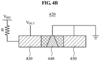
- FIG. 4B illustrates a cross section of an NPN BJT 420 according to an embodiment.
- a base region 440 and an emitter region 450 of the NPN BJT may be connected to a ground, and accordingly the NPN BJT may be turned off.
- a collector region 430 and the emitter region 450 may not be shorted.
- an output value may be "1" due to V DD connected to the collector region 450, instead of a ground voltage applied to the emitter region 430.
- a current may flow between the collector region 430 and the emitter region 450, and a voltage of the emitter region 450 may be an output value. Because the emitter region 450 of the NPN BJT 420 is connected to the ground, a voltage V CE between the collector region 430 and the emitter region 450 may have a value close to "0,” and the value of the voltage V CE may be regarded as an output value of "0.”
- a reader may determine whether a short circuit occurs in an NPN BJT, may output a value of "0" or "1" as an output value, and may provide an identification key.
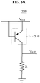
- FIG. 5A illustrates a circuit 500 of an identification key generation device including a PNP BJT according to an embodiment.
- a reader included in the identification key generation device with the PNP BJT may determine, based on an output value, whether an emitter region and a collector region of a PNP BJT 510 are shorted.
- An operation principle of the identification key generation device including the PNP BJT may be the same as the operation principle of the identification key generation device including the NPN BJT of FIG. 4 , except that the emitter region and a base region are connected to V DD and that the collector region is connected to the ground through a resistor.
- a voltage V CE between the collector region and the emitter region may have a value close to "0.”
- an output value may be regarded as "1" due to V DD applied to the emitter region.
- the output value may be read as "0" because the collector region is connected to the ground through the resistor.
- whether a short circuit occurs in a PNP BJT may also be randomly determined by the reader, and an identification key may be provided as an output value.
- whether the emitter region and the collector region are shorted may be probabilistically determined in a manufacturing process of the PNP BJT, and thus randomness and time-invariance may be guaranteed.
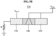
- FIG. 5B illustrates a cross section of a PNP BJT 520 according to an embodiment.
- a base region 540 and an emitter region 550 of the PNP BJT may be connected to V DD , and accordingly the PNP BJT may be turned off.
- a collector region 530 and the emitter region 550 may not be shorted.
- an output value may be "0" due to a ground connected to the collector region, instead of V DD applied to the emitter region.
- a voltage V CE between the collector region and the emitter region may have a value close to "0."
- an output value may be regarded as "1" due to V DD applied to the emitter region. Accordingly, even though the PNP BJT is turned off, the same voltage as V DD applied to the emitter region 550 may be transferred to the collector region 530, and the output value may be "1.”
- a reader may determine whether a short circuit occurs in a PNP BJT, may output a value of "0" or "1" as an output value, and may provide an identification key.
- FIG. 6 illustrates a parasitic NPN BJT 600 using an N-well and a P-substrate according to an embodiment.
- a parasitic BJT may be formed by various N+/P+ regions in a general complementary metal-oxide semiconductor (CMOS) process.
- CMOS complementary metal-oxide semiconductor
- the parasitic NPN BJT 600 may be formed using an N-well and a P-substrate in the general CMOS process.
- a collector region and an emitter region may be formed as N-wells 620, and a base region may be formed as a P-substrate 610.
- an interval equal to or greater than a predetermined interval between N-wells may be specified in a design rule.
- an interval between N-wells is formed to be equal to or greater than a first threshold and equal to or less than a second threshold as described above with reference to FIG. 3 , whether the collector region and the emitter region are shorted may be probabilistically determined by a process variation.
- the parasitic NPN BJT 600 may be used to generate a PUF.
- FIG. 7 illustrates a parasitic NPN BJT 700 using an N+ active region and a P+ active region according to an embodiment.
- the parasitic NPN BJT 700 may be formed using an N+ active region and a P+ active region in a general CMOS process.
- a collector region and an emitter region may be formed on a P-substrate 710.
- the collector region and the emitter region may be formed as N+ active regions 720, and a base region may be formed as a P+ active region 730.
- an interval equal to or greater than a predetermined interval between N+ active regions may be specified in a design rule.
- an interval between N+ active regions is formed to be equal to or greater than a first threshold and equal to or less than a second threshold as described above with reference to FIG. 3 , whether the collector region and the emitter region are shorted may be probabilistically determined by a process variation.
- the parasitic NPN BJT 700 may be used to generate a PUF.
- FIG. 8 illustrates a parasitic NPN BJT 800 using an N+ active region and a P-substrate according to an embodiment.
- the parasitic NPN BJT 800 may be formed using an N+ active region and a P-substrate.
- a collector region and an emitter region may be formed as N+ active regions 820, and a base region may be formed as a P-substrate 810.
- an interval equal to or greater than a predetermined interval between N+ active regions may be specified in a design rule.
- an interval between N+ active regions may be formed to be equal to or greater than a first threshold and equal to or less than a second threshold as described above with reference to FIG. 3 .
- the parasitic NPN BJT 800 may be used to generate a PUF.
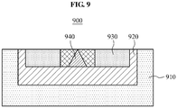
- FIG. 9 illustrates a parasitic PNP BJT 900 using an N+ active region and a P+ active region according to an embodiment.
- the parasitic PNP BJT 900 may be formed using an N+ active region and a P+ active region in a general CMOS process.
- a P-substrate 910 may surround an N-well 920. Also, an emitter region and a collector region may be formed as P+ active regions 930, and a base region may be formed as an N+ active region 940, in a CMOS process.
- an interval equal to or greater than a predetermined interval between P+ active regions may be specified in a design rule.
- an interval between P+ active regions may be formed to be equal to or greater than a first threshold and equal to or less than a second threshold as described above with reference to FIG. 3 .
- the parasitic PNP BJT 900 may be used to generate a PUF.
- FIG. 10 illustrates a parasitic PNP BJT 1000 using a P+ active region and an N-well according to an embodiment.
- the parasitic PNP BJT 1000 may be formed using a P+ active region and an N-well.
- a collector region and an emitter region may be formed as P+ active regions 1030, and a base region may be formed as an N-well 1020.
- a P-substrate 1010 may surround the N-well 1020.
- an interval equal to or greater than a predetermined interval between P+ active regions may be specified in a design rule.
- an interval between P+ active regions may be formed to be equal to or greater than a first threshold and equal to or less than a second threshold as described above with reference to FIG. 3 .
- the parasitic PNP BJT 1000 may be used to generate a PUF.
Priority Applications (1)
| Application Number | Priority Date | Filing Date | Title |
|---|---|---|---|
| EP19160788.6A EP3564843A1 (en) | 2013-09-03 | 2014-02-17 | Device and method for generating identification key |
Applications Claiming Priority (2)
| Application Number | Priority Date | Filing Date | Title |
|---|---|---|---|
| KR20130105470A KR101489088B1 (ko) | 2013-09-03 | 2013-09-03 | 식별키 생성 장치 및 방법 |
| PCT/KR2014/001255 WO2015034147A1 (ko) | 2013-09-03 | 2014-02-17 | 식별키 생성 장치 및 방법 |
Related Child Applications (2)
| Application Number | Title | Priority Date | Filing Date |
|---|---|---|---|
| EP19160788.6A Division EP3564843A1 (en) | 2013-09-03 | 2014-02-17 | Device and method for generating identification key |
| EP19160788.6A Division-Into EP3564843A1 (en) | 2013-09-03 | 2014-02-17 | Device and method for generating identification key |
Publications (3)
| Publication Number | Publication Date |
|---|---|
| EP3043283A1 EP3043283A1 (en) | 2016-07-13 |
| EP3043283A4 EP3043283A4 (en) | 2017-01-18 |
| EP3043283B1 true EP3043283B1 (en) | 2019-04-17 |
Family
ID=52590117
Family Applications (2)
| Application Number | Title | Priority Date | Filing Date |
|---|---|---|---|
| EP14842135.7A Active EP3043283B1 (en) | 2013-09-03 | 2014-02-17 | Device and method for generating identification key |
| EP19160788.6A Withdrawn EP3564843A1 (en) | 2013-09-03 | 2014-02-17 | Device and method for generating identification key |
Family Applications After (1)
| Application Number | Title | Priority Date | Filing Date |
|---|---|---|---|
| EP19160788.6A Withdrawn EP3564843A1 (en) | 2013-09-03 | 2014-02-17 | Device and method for generating identification key |
Country Status (4)
| Country | Link |
|---|---|
| US (3) | US10224295B2 (ko) |
| EP (2) | EP3043283B1 (ko) |
| KR (1) | KR101489088B1 (ko) |
| WO (1) | WO2015034147A1 (ko) |
Families Citing this family (2)
| Publication number | Priority date | Publication date | Assignee | Title |
|---|---|---|---|---|
| WO2015012667A1 (ko) | 2013-07-26 | 2015-01-29 | (주) 아이씨티케이 | 랜덤성 테스트 장치 및 방법 |
| US10685918B2 (en) | 2018-08-28 | 2020-06-16 | Semiconductor Components Industries, Llc | Process variation as die level traceability |
Citations (1)
| Publication number | Priority date | Publication date | Assignee | Title |
|---|---|---|---|---|
| US20130322617A1 (en) * | 2012-06-05 | 2013-12-05 | Board Of Regents, The University Of Texas System | Physically unclonable functions based on non-linearity of sub-threshold operation |
Family Cites Families (11)
| Publication number | Priority date | Publication date | Assignee | Title |
|---|---|---|---|---|
| JPH02312280A (ja) * | 1989-05-26 | 1990-12-27 | Mitsubishi Electric Corp | 絶縁ゲート型バイポーラトランジスタ |
| US6161213A (en) | 1999-02-17 | 2000-12-12 | Icid, Llc | System for providing an integrated circuit with a unique identification |
| FR2825873A1 (fr) * | 2001-06-11 | 2002-12-13 | St Microelectronics Sa | Stockage protege d'une donnee dans un circuit integre |
| US7840803B2 (en) * | 2002-04-16 | 2010-11-23 | Massachusetts Institute Of Technology | Authentication of integrated circuits |
| CN100438014C (zh) * | 2002-08-15 | 2008-11-26 | Nxp股份有限公司 | 集成电路及其制造方法 |
| KR100964845B1 (ko) * | 2007-11-29 | 2010-06-24 | 주식회사 시큐트론 | 공정편차에 기반한 보안 시스템 및 방법 |
| US9703806B2 (en) * | 2008-06-17 | 2017-07-11 | Microsoft Technology Licensing, Llc | User photo handling and control |
| US8619979B2 (en) * | 2010-06-25 | 2013-12-31 | International Business Machines Corporation | Physically unclonable function implemented through threshold voltage comparison |
| KR101139630B1 (ko) | 2010-12-09 | 2012-05-30 | 한양대학교 산학협력단 | 식별키 생성 장치 및 방법 |
| US8744143B2 (en) * | 2011-04-01 | 2014-06-03 | Yahoo! Inc. | Adding privacy protection to photo uploading/ tagging in social networks |
| KR20120114186A (ko) * | 2012-05-29 | 2012-10-16 | 한양대학교 산학협력단 | 공정편차를 이용한 식별 키 생성 장치 및 방법 |
-
2013
- 2013-09-03 KR KR20130105470A patent/KR101489088B1/ko active IP Right Grant
-
2014
- 2014-02-17 WO PCT/KR2014/001255 patent/WO2015034147A1/ko active Application Filing
- 2014-02-17 EP EP14842135.7A patent/EP3043283B1/en active Active
- 2014-02-17 EP EP19160788.6A patent/EP3564843A1/en not_active Withdrawn
- 2014-02-17 US US14/916,492 patent/US10224295B2/en active Active
-
2019
- 2019-02-07 US US16/270,298 patent/US10629548B2/en active Active
- 2019-04-19 US US16/389,714 patent/US10629549B2/en active Active
Patent Citations (1)
| Publication number | Priority date | Publication date | Assignee | Title |
|---|---|---|---|---|
| US20130322617A1 (en) * | 2012-06-05 | 2013-12-05 | Board Of Regents, The University Of Texas System | Physically unclonable functions based on non-linearity of sub-threshold operation |
Also Published As
| Publication number | Publication date |
|---|---|
| KR101489088B1 (ko) | 2015-02-04 |
| EP3043283A4 (en) | 2017-01-18 |
| US20190244916A1 (en) | 2019-08-08 |
| US10629549B2 (en) | 2020-04-21 |
| WO2015034147A1 (ko) | 2015-03-12 |
| US10629548B2 (en) | 2020-04-21 |
| EP3564843A1 (en) | 2019-11-06 |
| US10224295B2 (en) | 2019-03-05 |
| US20160211232A1 (en) | 2016-07-21 |
| US20190172801A1 (en) | 2019-06-06 |
| EP3043283A1 (en) | 2016-07-13 |
Similar Documents
| Publication | Publication Date | Title |
|---|---|---|
| US9223368B2 (en) | Countermeasure method and device for protecting data circulating in an electronic microcircuit | |
| US9070697B2 (en) | Device for detecting a laser attack in an integrated circuit chip | |
| US9984982B2 (en) | Device and method for generating identification key | |
| US10770409B2 (en) | Method for detecting thinning of the substrate of an integrated circuit from its back side, and associated integrated circuit | |
| US10629548B2 (en) | Device and method for generating identification key | |
| US10833027B2 (en) | Integrated physically unclonable function device with a set of transistors exhibiting a random distribution of threshold voltages | |
| US9166588B2 (en) | Semiconductor device including enhanced variability | |
| US20140197865A1 (en) | On-chip randomness generation | |
| US10242950B2 (en) | Semiconductor device, method of manufacturing the same and generation method of unique information | |
| US9859228B2 (en) | Device and method for generating identification key | |
| US9838389B2 (en) | Integrated circuit, code generating method, and data exchange method | |
| KR102000617B1 (ko) | 식별키 생성 장치 및 방법 | |
| KR20150027014A (ko) | 식별키 생성 장치 및 방법 | |
| TW201806122A (zh) | 具有偽裝功能的半導體裝置 | |
| KR102048175B1 (ko) | 식별 키 생성 장치 및 방법 | |
| KR20150028756A (ko) | 식별 키 생성 장치 및 방법 | |
| US20020005526A1 (en) | Electrostatic discharge protective structure and a method for producing it |
Legal Events
| Date | Code | Title | Description |
|---|---|---|---|
| PUAI | Public reference made under article 153(3) epc to a published international application that has entered the european phase |
Free format text: ORIGINAL CODE: 0009012 |
|
| 17P | Request for examination filed |
Effective date: 20160317 |
|
| AK | Designated contracting states |
Kind code of ref document: A1 Designated state(s): AL AT BE BG CH CY CZ DE DK EE ES FI FR GB GR HR HU IE IS IT LI LT LU LV MC MK MT NL NO PL PT RO RS SE SI SK SM TR |
|
| AX | Request for extension of the european patent |
Extension state: BA ME |
|
| DAX | Request for extension of the european patent (deleted) | ||
| A4 | Supplementary search report drawn up and despatched |
Effective date: 20161221 |
|
| RIC1 | Information provided on ipc code assigned before grant |
Ipc: G06F 21/60 20130101AFI20161215BHEP |
|
| GRAP | Despatch of communication of intention to grant a patent |
Free format text: ORIGINAL CODE: EPIDOSNIGR1 |
|
| STAA | Information on the status of an ep patent application or granted ep patent |
Free format text: STATUS: GRANT OF PATENT IS INTENDED |
|
| INTG | Intention to grant announced |
Effective date: 20180523 |
|
| GRAJ | Information related to disapproval of communication of intention to grant by the applicant or resumption of examination proceedings by the epo deleted |
Free format text: ORIGINAL CODE: EPIDOSDIGR1 |
|
| STAA | Information on the status of an ep patent application or granted ep patent |
Free format text: STATUS: REQUEST FOR EXAMINATION WAS MADE |
|
| GRAP | Despatch of communication of intention to grant a patent |
Free format text: ORIGINAL CODE: EPIDOSNIGR1 |
|
| STAA | Information on the status of an ep patent application or granted ep patent |
Free format text: STATUS: GRANT OF PATENT IS INTENDED |
|
| INTC | Intention to grant announced (deleted) | ||
| INTG | Intention to grant announced |
Effective date: 20181106 |
|
| RAP1 | Party data changed (applicant data changed or rights of an application transferred) |
Owner name: ICTK HOLDINGS CO., LTD. |
|
| GRAS | Grant fee paid |
Free format text: ORIGINAL CODE: EPIDOSNIGR3 |
|
| GRAA | (expected) grant |
Free format text: ORIGINAL CODE: 0009210 |
|
| STAA | Information on the status of an ep patent application or granted ep patent |
Free format text: STATUS: THE PATENT HAS BEEN GRANTED |
|
| AK | Designated contracting states |
Kind code of ref document: B1 Designated state(s): AL AT BE BG CH CY CZ DE DK EE ES FI FR GB GR HR HU IE IS IT LI LT LU LV MC MK MT NL NO PL PT RO RS SE SI SK SM TR |
|
| REG | Reference to a national code |
Ref country code: GB Ref legal event code: FG4D |
|
| REG | Reference to a national code |
Ref country code: CH Ref legal event code: EP |
|
| REG | Reference to a national code |
Ref country code: DE Ref legal event code: R096 Ref document number: 602014045060 Country of ref document: DE |
|
| REG | Reference to a national code |
Ref country code: AT Ref legal event code: REF Ref document number: 1122366 Country of ref document: AT Kind code of ref document: T Effective date: 20190515 Ref country code: IE Ref legal event code: FG4D |
|
| REG | Reference to a national code |
Ref country code: NL Ref legal event code: FP |
|
| REG | Reference to a national code |
Ref country code: LT Ref legal event code: MG4D |
|
| PG25 | Lapsed in a contracting state [announced via postgrant information from national office to epo] |
Ref country code: SE Free format text: LAPSE BECAUSE OF FAILURE TO SUBMIT A TRANSLATION OF THE DESCRIPTION OR TO PAY THE FEE WITHIN THE PRESCRIBED TIME-LIMIT Effective date: 20190417 Ref country code: HR Free format text: LAPSE BECAUSE OF FAILURE TO SUBMIT A TRANSLATION OF THE DESCRIPTION OR TO PAY THE FEE WITHIN THE PRESCRIBED TIME-LIMIT Effective date: 20190417 Ref country code: ES Free format text: LAPSE BECAUSE OF FAILURE TO SUBMIT A TRANSLATION OF THE DESCRIPTION OR TO PAY THE FEE WITHIN THE PRESCRIBED TIME-LIMIT Effective date: 20190417 Ref country code: LT Free format text: LAPSE BECAUSE OF FAILURE TO SUBMIT A TRANSLATION OF THE DESCRIPTION OR TO PAY THE FEE WITHIN THE PRESCRIBED TIME-LIMIT Effective date: 20190417 Ref country code: AL Free format text: LAPSE BECAUSE OF FAILURE TO SUBMIT A TRANSLATION OF THE DESCRIPTION OR TO PAY THE FEE WITHIN THE PRESCRIBED TIME-LIMIT Effective date: 20190417 Ref country code: PT Free format text: LAPSE BECAUSE OF FAILURE TO SUBMIT A TRANSLATION OF THE DESCRIPTION OR TO PAY THE FEE WITHIN THE PRESCRIBED TIME-LIMIT Effective date: 20190817 Ref country code: NO Free format text: LAPSE BECAUSE OF FAILURE TO SUBMIT A TRANSLATION OF THE DESCRIPTION OR TO PAY THE FEE WITHIN THE PRESCRIBED TIME-LIMIT Effective date: 20190717 Ref country code: FI Free format text: LAPSE BECAUSE OF FAILURE TO SUBMIT A TRANSLATION OF THE DESCRIPTION OR TO PAY THE FEE WITHIN THE PRESCRIBED TIME-LIMIT Effective date: 20190417 |
|
| PG25 | Lapsed in a contracting state [announced via postgrant information from national office to epo] |
Ref country code: GR Free format text: LAPSE BECAUSE OF FAILURE TO SUBMIT A TRANSLATION OF THE DESCRIPTION OR TO PAY THE FEE WITHIN THE PRESCRIBED TIME-LIMIT Effective date: 20190718 Ref country code: BG Free format text: LAPSE BECAUSE OF FAILURE TO SUBMIT A TRANSLATION OF THE DESCRIPTION OR TO PAY THE FEE WITHIN THE PRESCRIBED TIME-LIMIT Effective date: 20190717 Ref country code: PL Free format text: LAPSE BECAUSE OF FAILURE TO SUBMIT A TRANSLATION OF THE DESCRIPTION OR TO PAY THE FEE WITHIN THE PRESCRIBED TIME-LIMIT Effective date: 20190417 Ref country code: LV Free format text: LAPSE BECAUSE OF FAILURE TO SUBMIT A TRANSLATION OF THE DESCRIPTION OR TO PAY THE FEE WITHIN THE PRESCRIBED TIME-LIMIT Effective date: 20190417 Ref country code: RS Free format text: LAPSE BECAUSE OF FAILURE TO SUBMIT A TRANSLATION OF THE DESCRIPTION OR TO PAY THE FEE WITHIN THE PRESCRIBED TIME-LIMIT Effective date: 20190417 |
|
| REG | Reference to a national code |
Ref country code: AT Ref legal event code: MK05 Ref document number: 1122366 Country of ref document: AT Kind code of ref document: T Effective date: 20190417 |
|
| PG25 | Lapsed in a contracting state [announced via postgrant information from national office to epo] |
Ref country code: IS Free format text: LAPSE BECAUSE OF FAILURE TO SUBMIT A TRANSLATION OF THE DESCRIPTION OR TO PAY THE FEE WITHIN THE PRESCRIBED TIME-LIMIT Effective date: 20190817 |
|
| REG | Reference to a national code |
Ref country code: DE Ref legal event code: R097 Ref document number: 602014045060 Country of ref document: DE |
|
| PG25 | Lapsed in a contracting state [announced via postgrant information from national office to epo] |
Ref country code: EE Free format text: LAPSE BECAUSE OF FAILURE TO SUBMIT A TRANSLATION OF THE DESCRIPTION OR TO PAY THE FEE WITHIN THE PRESCRIBED TIME-LIMIT Effective date: 20190417 Ref country code: CZ Free format text: LAPSE BECAUSE OF FAILURE TO SUBMIT A TRANSLATION OF THE DESCRIPTION OR TO PAY THE FEE WITHIN THE PRESCRIBED TIME-LIMIT Effective date: 20190417 Ref country code: RO Free format text: LAPSE BECAUSE OF FAILURE TO SUBMIT A TRANSLATION OF THE DESCRIPTION OR TO PAY THE FEE WITHIN THE PRESCRIBED TIME-LIMIT Effective date: 20190417 Ref country code: SK Free format text: LAPSE BECAUSE OF FAILURE TO SUBMIT A TRANSLATION OF THE DESCRIPTION OR TO PAY THE FEE WITHIN THE PRESCRIBED TIME-LIMIT Effective date: 20190417 Ref country code: AT Free format text: LAPSE BECAUSE OF FAILURE TO SUBMIT A TRANSLATION OF THE DESCRIPTION OR TO PAY THE FEE WITHIN THE PRESCRIBED TIME-LIMIT Effective date: 20190417 Ref country code: DK Free format text: LAPSE BECAUSE OF FAILURE TO SUBMIT A TRANSLATION OF THE DESCRIPTION OR TO PAY THE FEE WITHIN THE PRESCRIBED TIME-LIMIT Effective date: 20190417 |
|
| PLBE | No opposition filed within time limit |
Free format text: ORIGINAL CODE: 0009261 |
|
| STAA | Information on the status of an ep patent application or granted ep patent |
Free format text: STATUS: NO OPPOSITION FILED WITHIN TIME LIMIT |
|
| PG25 | Lapsed in a contracting state [announced via postgrant information from national office to epo] |
Ref country code: SM Free format text: LAPSE BECAUSE OF FAILURE TO SUBMIT A TRANSLATION OF THE DESCRIPTION OR TO PAY THE FEE WITHIN THE PRESCRIBED TIME-LIMIT Effective date: 20190417 Ref country code: IT Free format text: LAPSE BECAUSE OF FAILURE TO SUBMIT A TRANSLATION OF THE DESCRIPTION OR TO PAY THE FEE WITHIN THE PRESCRIBED TIME-LIMIT Effective date: 20190417 |
|
| 26N | No opposition filed |
Effective date: 20200120 |
|
| PG25 | Lapsed in a contracting state [announced via postgrant information from national office to epo] |
Ref country code: TR Free format text: LAPSE BECAUSE OF FAILURE TO SUBMIT A TRANSLATION OF THE DESCRIPTION OR TO PAY THE FEE WITHIN THE PRESCRIBED TIME-LIMIT Effective date: 20190417 |
|
| PGFP | Annual fee paid to national office [announced via postgrant information from national office to epo] |
Ref country code: NL Payment date: 20200212 Year of fee payment: 7 |
|
| PG25 | Lapsed in a contracting state [announced via postgrant information from national office to epo] |
Ref country code: SI Free format text: LAPSE BECAUSE OF FAILURE TO SUBMIT A TRANSLATION OF THE DESCRIPTION OR TO PAY THE FEE WITHIN THE PRESCRIBED TIME-LIMIT Effective date: 20190417 |
|
| PGFP | Annual fee paid to national office [announced via postgrant information from national office to epo] |
Ref country code: BE Payment date: 20200123 Year of fee payment: 7 Ref country code: CH Payment date: 20200213 Year of fee payment: 7 Ref country code: LU Payment date: 20200210 Year of fee payment: 7 |
|
| PG25 | Lapsed in a contracting state [announced via postgrant information from national office to epo] |
Ref country code: MC Free format text: LAPSE BECAUSE OF FAILURE TO SUBMIT A TRANSLATION OF THE DESCRIPTION OR TO PAY THE FEE WITHIN THE PRESCRIBED TIME-LIMIT Effective date: 20190417 |
|
| PG25 | Lapsed in a contracting state [announced via postgrant information from national office to epo] |
Ref country code: IE Free format text: LAPSE BECAUSE OF NON-PAYMENT OF DUE FEES Effective date: 20200217 |
|
| REG | Reference to a national code |
Ref country code: BE Ref legal event code: MM Effective date: 20210228 |
|
| PG25 | Lapsed in a contracting state [announced via postgrant information from national office to epo] |
Ref country code: LI Free format text: LAPSE BECAUSE OF NON-PAYMENT OF DUE FEES Effective date: 20210228 Ref country code: LU Free format text: LAPSE BECAUSE OF NON-PAYMENT OF DUE FEES Effective date: 20210217 Ref country code: CH Free format text: LAPSE BECAUSE OF NON-PAYMENT OF DUE FEES Effective date: 20210228 |
|
| REG | Reference to a national code |
Ref country code: NL Ref legal event code: MM Effective date: 20210301 |
|
| PG25 | Lapsed in a contracting state [announced via postgrant information from national office to epo] |
Ref country code: NL Free format text: LAPSE BECAUSE OF NON-PAYMENT OF DUE FEES Effective date: 20210301 |
|
| PG25 | Lapsed in a contracting state [announced via postgrant information from national office to epo] |
Ref country code: MT Free format text: LAPSE BECAUSE OF FAILURE TO SUBMIT A TRANSLATION OF THE DESCRIPTION OR TO PAY THE FEE WITHIN THE PRESCRIBED TIME-LIMIT Effective date: 20190417 Ref country code: CY Free format text: LAPSE BECAUSE OF FAILURE TO SUBMIT A TRANSLATION OF THE DESCRIPTION OR TO PAY THE FEE WITHIN THE PRESCRIBED TIME-LIMIT Effective date: 20190417 |
|
| PG25 | Lapsed in a contracting state [announced via postgrant information from national office to epo] |
Ref country code: MK Free format text: LAPSE BECAUSE OF FAILURE TO SUBMIT A TRANSLATION OF THE DESCRIPTION OR TO PAY THE FEE WITHIN THE PRESCRIBED TIME-LIMIT Effective date: 20190417 |
|
| PG25 | Lapsed in a contracting state [announced via postgrant information from national office to epo] |
Ref country code: BE Free format text: LAPSE BECAUSE OF NON-PAYMENT OF DUE FEES Effective date: 20210228 |
|
| PGFP | Annual fee paid to national office [announced via postgrant information from national office to epo] |
Ref country code: DE Payment date: 20221220 Year of fee payment: 10 |
|
| PGFP | Annual fee paid to national office [announced via postgrant information from national office to epo] |
Ref country code: GB Payment date: 20231220 Year of fee payment: 11 |
|
| PGFP | Annual fee paid to national office [announced via postgrant information from national office to epo] |
Ref country code: FR Payment date: 20231222 Year of fee payment: 11 |