EP3040442A1 - Hybrid organic/inorganic thin films and method of manufacturing same - Google Patents
Hybrid organic/inorganic thin films and method of manufacturing same Download PDFInfo
- Publication number
- EP3040442A1 EP3040442A1 EP13892196.0A EP13892196A EP3040442A1 EP 3040442 A1 EP3040442 A1 EP 3040442A1 EP 13892196 A EP13892196 A EP 13892196A EP 3040442 A1 EP3040442 A1 EP 3040442A1
- Authority
- EP
- European Patent Office
- Prior art keywords
- thin film
- organic
- inorganic hybrid
- group
- hybrid thin
- Prior art date
- Legal status (The legal status is an assumption and is not a legal conclusion. Google has not performed a legal analysis and makes no representation as to the accuracy of the status listed.)
- Granted
Links
Images


Classifications
-
- H—ELECTRICITY
- H10—SEMICONDUCTOR DEVICES; ELECTRIC SOLID-STATE DEVICES NOT OTHERWISE PROVIDED FOR
- H10W—GENERIC PACKAGES, INTERCONNECTIONS, CONNECTORS OR OTHER CONSTRUCTIONAL DETAILS OF DEVICES COVERED BY CLASS H10
- H10W74/00—Encapsulations, e.g. protective coatings
- H10W74/10—Encapsulations, e.g. protective coatings characterised by their shape or disposition
- H10W74/131—Encapsulations, e.g. protective coatings characterised by their shape or disposition the semiconductor body being only partially enclosed
- H10W74/147—Encapsulations, e.g. protective coatings characterised by their shape or disposition the semiconductor body being only partially enclosed the encapsulations being multilayered
-
- B—PERFORMING OPERATIONS; TRANSPORTING
- B32—LAYERED PRODUCTS
- B32B—LAYERED PRODUCTS, i.e. PRODUCTS BUILT-UP OF STRATA OF FLAT OR NON-FLAT, e.g. CELLULAR OR HONEYCOMB, FORM
- B32B7/00—Layered products characterised by the relation between layers; Layered products characterised by the relative orientation of features between layers, or by the relative values of a measurable parameter between layers, i.e. products comprising layers having different physical, chemical or physicochemical properties; Layered products characterised by the interconnection of layers
- B32B7/02—Physical, chemical or physicochemical properties
-
- B—PERFORMING OPERATIONS; TRANSPORTING
- B32—LAYERED PRODUCTS
- B32B—LAYERED PRODUCTS, i.e. PRODUCTS BUILT-UP OF STRATA OF FLAT OR NON-FLAT, e.g. CELLULAR OR HONEYCOMB, FORM
- B32B15/00—Layered products comprising a layer of metal
- B32B15/04—Layered products comprising a layer of metal comprising metal as the main or only constituent of a layer, which is next to another layer of the same or of a different material
-
- C—CHEMISTRY; METALLURGY
- C07—ORGANIC CHEMISTRY
- C07F—ACYCLIC, CARBOCYCLIC OR HETEROCYCLIC COMPOUNDS CONTAINING ELEMENTS OTHER THAN CARBON, HYDROGEN, HALOGEN, OXYGEN, NITROGEN, SULFUR, SELENIUM OR TELLURIUM
- C07F3/00—Compounds containing elements of Groups 2 or 12 of the Periodic Table
- C07F3/06—Zinc compounds
-
- C—CHEMISTRY; METALLURGY
- C07—ORGANIC CHEMISTRY
- C07F—ACYCLIC, CARBOCYCLIC OR HETEROCYCLIC COMPOUNDS CONTAINING ELEMENTS OTHER THAN CARBON, HYDROGEN, HALOGEN, OXYGEN, NITROGEN, SULFUR, SELENIUM OR TELLURIUM
- C07F5/00—Compounds containing elements of Groups 3 or 13 of the Periodic Table
- C07F5/06—Aluminium compounds
- C07F5/061—Aluminium compounds with C-aluminium linkage
- C07F5/062—Al linked exclusively to C
-
- C—CHEMISTRY; METALLURGY
- C23—COATING METALLIC MATERIAL; COATING MATERIAL WITH METALLIC MATERIAL; CHEMICAL SURFACE TREATMENT; DIFFUSION TREATMENT OF METALLIC MATERIAL; COATING BY VACUUM EVAPORATION, BY SPUTTERING, BY ION IMPLANTATION OR BY CHEMICAL VAPOUR DEPOSITION, IN GENERAL; INHIBITING CORROSION OF METALLIC MATERIAL OR INCRUSTATION IN GENERAL
- C23C—COATING METALLIC MATERIAL; COATING MATERIAL WITH METALLIC MATERIAL; SURFACE TREATMENT OF METALLIC MATERIAL BY DIFFUSION INTO THE SURFACE, BY CHEMICAL CONVERSION OR SUBSTITUTION; COATING BY VACUUM EVAPORATION, BY SPUTTERING, BY ION IMPLANTATION OR BY CHEMICAL VAPOUR DEPOSITION, IN GENERAL
- C23C16/00—Chemical coating by decomposition of gaseous compounds, without leaving reaction products of surface material in the coating, i.e. chemical vapour deposition [CVD] processes
-
- C—CHEMISTRY; METALLURGY
- C23—COATING METALLIC MATERIAL; COATING MATERIAL WITH METALLIC MATERIAL; CHEMICAL SURFACE TREATMENT; DIFFUSION TREATMENT OF METALLIC MATERIAL; COATING BY VACUUM EVAPORATION, BY SPUTTERING, BY ION IMPLANTATION OR BY CHEMICAL VAPOUR DEPOSITION, IN GENERAL; INHIBITING CORROSION OF METALLIC MATERIAL OR INCRUSTATION IN GENERAL
- C23C—COATING METALLIC MATERIAL; COATING MATERIAL WITH METALLIC MATERIAL; SURFACE TREATMENT OF METALLIC MATERIAL BY DIFFUSION INTO THE SURFACE, BY CHEMICAL CONVERSION OR SUBSTITUTION; COATING BY VACUUM EVAPORATION, BY SPUTTERING, BY ION IMPLANTATION OR BY CHEMICAL VAPOUR DEPOSITION, IN GENERAL
- C23C16/00—Chemical coating by decomposition of gaseous compounds, without leaving reaction products of surface material in the coating, i.e. chemical vapour deposition [CVD] processes
- C23C16/22—Chemical coating by decomposition of gaseous compounds, without leaving reaction products of surface material in the coating, i.e. chemical vapour deposition [CVD] processes characterised by the deposition of inorganic material, other than metallic material
- C23C16/30—Deposition of compounds, mixtures or solid solutions, e.g. borides, carbides, nitrides
- C23C16/42—Silicides
-
- C—CHEMISTRY; METALLURGY
- C23—COATING METALLIC MATERIAL; COATING MATERIAL WITH METALLIC MATERIAL; CHEMICAL SURFACE TREATMENT; DIFFUSION TREATMENT OF METALLIC MATERIAL; COATING BY VACUUM EVAPORATION, BY SPUTTERING, BY ION IMPLANTATION OR BY CHEMICAL VAPOUR DEPOSITION, IN GENERAL; INHIBITING CORROSION OF METALLIC MATERIAL OR INCRUSTATION IN GENERAL
- C23C—COATING METALLIC MATERIAL; COATING MATERIAL WITH METALLIC MATERIAL; SURFACE TREATMENT OF METALLIC MATERIAL BY DIFFUSION INTO THE SURFACE, BY CHEMICAL CONVERSION OR SUBSTITUTION; COATING BY VACUUM EVAPORATION, BY SPUTTERING, BY ION IMPLANTATION OR BY CHEMICAL VAPOUR DEPOSITION, IN GENERAL
- C23C16/00—Chemical coating by decomposition of gaseous compounds, without leaving reaction products of surface material in the coating, i.e. chemical vapour deposition [CVD] processes
- C23C16/44—Chemical coating by decomposition of gaseous compounds, without leaving reaction products of surface material in the coating, i.e. chemical vapour deposition [CVD] processes characterised by the method of coating
- C23C16/448—Chemical coating by decomposition of gaseous compounds, without leaving reaction products of surface material in the coating, i.e. chemical vapour deposition [CVD] processes characterised by the method of coating characterised by the method used for generating reactive gas streams, e.g. by evaporation or sublimation of precursor materials
-
- C—CHEMISTRY; METALLURGY
- C23—COATING METALLIC MATERIAL; COATING MATERIAL WITH METALLIC MATERIAL; CHEMICAL SURFACE TREATMENT; DIFFUSION TREATMENT OF METALLIC MATERIAL; COATING BY VACUUM EVAPORATION, BY SPUTTERING, BY ION IMPLANTATION OR BY CHEMICAL VAPOUR DEPOSITION, IN GENERAL; INHIBITING CORROSION OF METALLIC MATERIAL OR INCRUSTATION IN GENERAL
- C23C—COATING METALLIC MATERIAL; COATING MATERIAL WITH METALLIC MATERIAL; SURFACE TREATMENT OF METALLIC MATERIAL BY DIFFUSION INTO THE SURFACE, BY CHEMICAL CONVERSION OR SUBSTITUTION; COATING BY VACUUM EVAPORATION, BY SPUTTERING, BY ION IMPLANTATION OR BY CHEMICAL VAPOUR DEPOSITION, IN GENERAL
- C23C16/00—Chemical coating by decomposition of gaseous compounds, without leaving reaction products of surface material in the coating, i.e. chemical vapour deposition [CVD] processes
- C23C16/44—Chemical coating by decomposition of gaseous compounds, without leaving reaction products of surface material in the coating, i.e. chemical vapour deposition [CVD] processes characterised by the method of coating
- C23C16/455—Chemical coating by decomposition of gaseous compounds, without leaving reaction products of surface material in the coating, i.e. chemical vapour deposition [CVD] processes characterised by the method of coating characterised by the method used for introducing gases into reaction chamber or for modifying gas flows in reaction chamber
- C23C16/45523—Pulsed gas flow or change of composition over time
- C23C16/45525—Atomic layer deposition [ALD]
- C23C16/45527—Atomic layer deposition [ALD] characterized by the ALD cycle, e.g. different flows or temperatures during half-reactions, unusual pulsing sequence, use of precursor mixtures or auxiliary reactants or activations
- C23C16/45529—Atomic layer deposition [ALD] characterized by the ALD cycle, e.g. different flows or temperatures during half-reactions, unusual pulsing sequence, use of precursor mixtures or auxiliary reactants or activations specially adapted for making a layer stack of alternating different compositions or gradient compositions
-
- C—CHEMISTRY; METALLURGY
- C23—COATING METALLIC MATERIAL; COATING MATERIAL WITH METALLIC MATERIAL; CHEMICAL SURFACE TREATMENT; DIFFUSION TREATMENT OF METALLIC MATERIAL; COATING BY VACUUM EVAPORATION, BY SPUTTERING, BY ION IMPLANTATION OR BY CHEMICAL VAPOUR DEPOSITION, IN GENERAL; INHIBITING CORROSION OF METALLIC MATERIAL OR INCRUSTATION IN GENERAL
- C23C—COATING METALLIC MATERIAL; COATING MATERIAL WITH METALLIC MATERIAL; SURFACE TREATMENT OF METALLIC MATERIAL BY DIFFUSION INTO THE SURFACE, BY CHEMICAL CONVERSION OR SUBSTITUTION; COATING BY VACUUM EVAPORATION, BY SPUTTERING, BY ION IMPLANTATION OR BY CHEMICAL VAPOUR DEPOSITION, IN GENERAL
- C23C16/00—Chemical coating by decomposition of gaseous compounds, without leaving reaction products of surface material in the coating, i.e. chemical vapour deposition [CVD] processes
- C23C16/44—Chemical coating by decomposition of gaseous compounds, without leaving reaction products of surface material in the coating, i.e. chemical vapour deposition [CVD] processes characterised by the method of coating
- C23C16/455—Chemical coating by decomposition of gaseous compounds, without leaving reaction products of surface material in the coating, i.e. chemical vapour deposition [CVD] processes characterised by the method of coating characterised by the method used for introducing gases into reaction chamber or for modifying gas flows in reaction chamber
- C23C16/45523—Pulsed gas flow or change of composition over time
- C23C16/45525—Atomic layer deposition [ALD]
- C23C16/45553—Atomic layer deposition [ALD] characterized by the use of precursors specially adapted for ALD
-
- G—PHYSICS
- G02—OPTICS
- G02F—OPTICAL DEVICES OR ARRANGEMENTS FOR THE CONTROL OF LIGHT BY MODIFICATION OF THE OPTICAL PROPERTIES OF THE MEDIA OF THE ELEMENTS INVOLVED THEREIN; NON-LINEAR OPTICS; FREQUENCY-CHANGING OF LIGHT; OPTICAL LOGIC ELEMENTS; OPTICAL ANALOGUE/DIGITAL CONVERTERS
- G02F1/00—Devices or arrangements for the control of the intensity, colour, phase, polarisation or direction of light arriving from an independent light source, e.g. switching, gating or modulating; Non-linear optics
- G02F1/01—Devices or arrangements for the control of the intensity, colour, phase, polarisation or direction of light arriving from an independent light source, e.g. switching, gating or modulating; Non-linear optics for the control of the intensity, phase, polarisation or colour
- G02F1/13—Devices or arrangements for the control of the intensity, colour, phase, polarisation or direction of light arriving from an independent light source, e.g. switching, gating or modulating; Non-linear optics for the control of the intensity, phase, polarisation or colour based on liquid crystals, e.g. single liquid crystal display cells
- G02F1/133—Constructional arrangements; Operation of liquid crystal cells; Circuit arrangements
- G02F1/1333—Constructional arrangements; Manufacturing methods
-
- G—PHYSICS
- G02—OPTICS
- G02F—OPTICAL DEVICES OR ARRANGEMENTS FOR THE CONTROL OF LIGHT BY MODIFICATION OF THE OPTICAL PROPERTIES OF THE MEDIA OF THE ELEMENTS INVOLVED THEREIN; NON-LINEAR OPTICS; FREQUENCY-CHANGING OF LIGHT; OPTICAL LOGIC ELEMENTS; OPTICAL ANALOGUE/DIGITAL CONVERTERS
- G02F1/00—Devices or arrangements for the control of the intensity, colour, phase, polarisation or direction of light arriving from an independent light source, e.g. switching, gating or modulating; Non-linear optics
- G02F1/01—Devices or arrangements for the control of the intensity, colour, phase, polarisation or direction of light arriving from an independent light source, e.g. switching, gating or modulating; Non-linear optics for the control of the intensity, phase, polarisation or colour
- G02F1/13—Devices or arrangements for the control of the intensity, colour, phase, polarisation or direction of light arriving from an independent light source, e.g. switching, gating or modulating; Non-linear optics for the control of the intensity, phase, polarisation or colour based on liquid crystals, e.g. single liquid crystal display cells
- G02F1/133—Constructional arrangements; Operation of liquid crystal cells; Circuit arrangements
- G02F1/1333—Constructional arrangements; Manufacturing methods
- G02F1/133305—Flexible substrates, e.g. plastics, organic film
-
- H—ELECTRICITY
- H10—SEMICONDUCTOR DEVICES; ELECTRIC SOLID-STATE DEVICES NOT OTHERWISE PROVIDED FOR
- H10F—INORGANIC SEMICONDUCTOR DEVICES SENSITIVE TO INFRARED RADIATION, LIGHT, ELECTROMAGNETIC RADIATION OF SHORTER WAVELENGTH OR CORPUSCULAR RADIATION
- H10F77/00—Constructional details of devices covered by this subclass
- H10F77/50—Encapsulations or containers
-
- H—ELECTRICITY
- H10—SEMICONDUCTOR DEVICES; ELECTRIC SOLID-STATE DEVICES NOT OTHERWISE PROVIDED FOR
- H10K—ORGANIC ELECTRIC SOLID-STATE DEVICES
- H10K77/00—Constructional details of devices covered by this subclass and not covered by groups H10K10/80, H10K30/80, H10K50/80 or H10K59/80
- H10K77/10—Substrates, e.g. flexible substrates
-
- H—ELECTRICITY
- H10—SEMICONDUCTOR DEVICES; ELECTRIC SOLID-STATE DEVICES NOT OTHERWISE PROVIDED FOR
- H10K—ORGANIC ELECTRIC SOLID-STATE DEVICES
- H10K85/00—Organic materials used in the body or electrodes of devices covered by this subclass
- H10K85/10—Organic polymers or oligomers
-
- H—ELECTRICITY
- H10—SEMICONDUCTOR DEVICES; ELECTRIC SOLID-STATE DEVICES NOT OTHERWISE PROVIDED FOR
- H10K—ORGANIC ELECTRIC SOLID-STATE DEVICES
- H10K85/00—Organic materials used in the body or electrodes of devices covered by this subclass
- H10K85/60—Organic compounds having low molecular weight
-
- H—ELECTRICITY
- H10—SEMICONDUCTOR DEVICES; ELECTRIC SOLID-STATE DEVICES NOT OTHERWISE PROVIDED FOR
- H10W—GENERIC PACKAGES, INTERCONNECTIONS, CONNECTORS OR OTHER CONSTRUCTIONAL DETAILS OF DEVICES COVERED BY CLASS H10
- H10W74/00—Encapsulations, e.g. protective coatings
- H10W74/01—Manufacture or treatment
- H10W74/012—Manufacture or treatment of encapsulations on active surfaces of flip-chip devices, e.g. forming underfills
-
- H—ELECTRICITY
- H10—SEMICONDUCTOR DEVICES; ELECTRIC SOLID-STATE DEVICES NOT OTHERWISE PROVIDED FOR
- H10W—GENERIC PACKAGES, INTERCONNECTIONS, CONNECTORS OR OTHER CONSTRUCTIONAL DETAILS OF DEVICES COVERED BY CLASS H10
- H10W74/00—Encapsulations, e.g. protective coatings
- H10W74/10—Encapsulations, e.g. protective coatings characterised by their shape or disposition
- H10W74/15—Encapsulations, e.g. protective coatings characterised by their shape or disposition on active surfaces of flip-chip devices, e.g. underfills
-
- H—ELECTRICITY
- H10—SEMICONDUCTOR DEVICES; ELECTRIC SOLID-STATE DEVICES NOT OTHERWISE PROVIDED FOR
- H10W—GENERIC PACKAGES, INTERCONNECTIONS, CONNECTORS OR OTHER CONSTRUCTIONAL DETAILS OF DEVICES COVERED BY CLASS H10
- H10W74/00—Encapsulations, e.g. protective coatings
- H10W74/40—Encapsulations, e.g. protective coatings characterised by their materials
- H10W74/47—Encapsulations, e.g. protective coatings characterised by their materials comprising organic materials, e.g. plastics or resins
-
- G—PHYSICS
- G02—OPTICS
- G02F—OPTICAL DEVICES OR ARRANGEMENTS FOR THE CONTROL OF LIGHT BY MODIFICATION OF THE OPTICAL PROPERTIES OF THE MEDIA OF THE ELEMENTS INVOLVED THEREIN; NON-LINEAR OPTICS; FREQUENCY-CHANGING OF LIGHT; OPTICAL LOGIC ELEMENTS; OPTICAL ANALOGUE/DIGITAL CONVERTERS
- G02F1/00—Devices or arrangements for the control of the intensity, colour, phase, polarisation or direction of light arriving from an independent light source, e.g. switching, gating or modulating; Non-linear optics
- G02F1/01—Devices or arrangements for the control of the intensity, colour, phase, polarisation or direction of light arriving from an independent light source, e.g. switching, gating or modulating; Non-linear optics for the control of the intensity, phase, polarisation or colour
- G02F1/13—Devices or arrangements for the control of the intensity, colour, phase, polarisation or direction of light arriving from an independent light source, e.g. switching, gating or modulating; Non-linear optics for the control of the intensity, phase, polarisation or colour based on liquid crystals, e.g. single liquid crystal display cells
- G02F1/133—Constructional arrangements; Operation of liquid crystal cells; Circuit arrangements
- G02F1/1333—Constructional arrangements; Manufacturing methods
- G02F1/133302—Rigid substrates, e.g. inorganic substrates
-
- G—PHYSICS
- G02—OPTICS
- G02F—OPTICAL DEVICES OR ARRANGEMENTS FOR THE CONTROL OF LIGHT BY MODIFICATION OF THE OPTICAL PROPERTIES OF THE MEDIA OF THE ELEMENTS INVOLVED THEREIN; NON-LINEAR OPTICS; FREQUENCY-CHANGING OF LIGHT; OPTICAL LOGIC ELEMENTS; OPTICAL ANALOGUE/DIGITAL CONVERTERS
- G02F1/00—Devices or arrangements for the control of the intensity, colour, phase, polarisation or direction of light arriving from an independent light source, e.g. switching, gating or modulating; Non-linear optics
- G02F1/01—Devices or arrangements for the control of the intensity, colour, phase, polarisation or direction of light arriving from an independent light source, e.g. switching, gating or modulating; Non-linear optics for the control of the intensity, phase, polarisation or colour
- G02F1/13—Devices or arrangements for the control of the intensity, colour, phase, polarisation or direction of light arriving from an independent light source, e.g. switching, gating or modulating; Non-linear optics for the control of the intensity, phase, polarisation or colour based on liquid crystals, e.g. single liquid crystal display cells
- G02F1/133—Constructional arrangements; Operation of liquid crystal cells; Circuit arrangements
- G02F1/1333—Constructional arrangements; Manufacturing methods
- G02F1/133345—Insulating layers
-
- G—PHYSICS
- G02—OPTICS
- G02F—OPTICAL DEVICES OR ARRANGEMENTS FOR THE CONTROL OF LIGHT BY MODIFICATION OF THE OPTICAL PROPERTIES OF THE MEDIA OF THE ELEMENTS INVOLVED THEREIN; NON-LINEAR OPTICS; FREQUENCY-CHANGING OF LIGHT; OPTICAL LOGIC ELEMENTS; OPTICAL ANALOGUE/DIGITAL CONVERTERS
- G02F2201/00—Constructional arrangements not provided for in groups G02F1/00 - G02F7/00
- G02F2201/50—Protective arrangements
- G02F2201/501—Blocking layers, e.g. against migration of ions
-
- G—PHYSICS
- G02—OPTICS
- G02F—OPTICAL DEVICES OR ARRANGEMENTS FOR THE CONTROL OF LIGHT BY MODIFICATION OF THE OPTICAL PROPERTIES OF THE MEDIA OF THE ELEMENTS INVOLVED THEREIN; NON-LINEAR OPTICS; FREQUENCY-CHANGING OF LIGHT; OPTICAL LOGIC ELEMENTS; OPTICAL ANALOGUE/DIGITAL CONVERTERS
- G02F2202/00—Materials and properties
- G02F2202/02—Materials and properties organic material
- G02F2202/022—Materials and properties organic material polymeric
-
- H—ELECTRICITY
- H10—SEMICONDUCTOR DEVICES; ELECTRIC SOLID-STATE DEVICES NOT OTHERWISE PROVIDED FOR
- H10K—ORGANIC ELECTRIC SOLID-STATE DEVICES
- H10K2102/00—Constructional details relating to the organic devices covered by this subclass
-
- H—ELECTRICITY
- H10—SEMICONDUCTOR DEVICES; ELECTRIC SOLID-STATE DEVICES NOT OTHERWISE PROVIDED FOR
- H10K—ORGANIC ELECTRIC SOLID-STATE DEVICES
- H10K2102/00—Constructional details relating to the organic devices covered by this subclass
- H10K2102/10—Transparent electrodes, e.g. using graphene
- H10K2102/101—Transparent electrodes, e.g. using graphene comprising transparent conductive oxides [TCO]
-
- H—ELECTRICITY
- H10—SEMICONDUCTOR DEVICES; ELECTRIC SOLID-STATE DEVICES NOT OTHERWISE PROVIDED FOR
- H10K—ORGANIC ELECTRIC SOLID-STATE DEVICES
- H10K2102/00—Constructional details relating to the organic devices covered by this subclass
- H10K2102/10—Transparent electrodes, e.g. using graphene
- H10K2102/101—Transparent electrodes, e.g. using graphene comprising transparent conductive oxides [TCO]
- H10K2102/103—Transparent electrodes, e.g. using graphene comprising transparent conductive oxides [TCO] comprising indium oxides, e.g. ITO
-
- H—ELECTRICITY
- H10—SEMICONDUCTOR DEVICES; ELECTRIC SOLID-STATE DEVICES NOT OTHERWISE PROVIDED FOR
- H10K—ORGANIC ELECTRIC SOLID-STATE DEVICES
- H10K2102/00—Constructional details relating to the organic devices covered by this subclass
- H10K2102/301—Details of OLEDs
- H10K2102/351—Thickness
-
- Y—GENERAL TAGGING OF NEW TECHNOLOGICAL DEVELOPMENTS; GENERAL TAGGING OF CROSS-SECTIONAL TECHNOLOGIES SPANNING OVER SEVERAL SECTIONS OF THE IPC; TECHNICAL SUBJECTS COVERED BY FORMER USPC CROSS-REFERENCE ART COLLECTIONS [XRACs] AND DIGESTS
- Y02—TECHNOLOGIES OR APPLICATIONS FOR MITIGATION OR ADAPTATION AGAINST CLIMATE CHANGE
- Y02E—REDUCTION OF GREENHOUSE GAS [GHG] EMISSIONS, RELATED TO ENERGY GENERATION, TRANSMISSION OR DISTRIBUTION
- Y02E10/00—Energy generation through renewable energy sources
- Y02E10/50—Photovoltaic [PV] energy
- Y02E10/549—Organic PV cells
-
- Y—GENERAL TAGGING OF NEW TECHNOLOGICAL DEVELOPMENTS; GENERAL TAGGING OF CROSS-SECTIONAL TECHNOLOGIES SPANNING OVER SEVERAL SECTIONS OF THE IPC; TECHNICAL SUBJECTS COVERED BY FORMER USPC CROSS-REFERENCE ART COLLECTIONS [XRACs] AND DIGESTS
- Y02—TECHNOLOGIES OR APPLICATIONS FOR MITIGATION OR ADAPTATION AGAINST CLIMATE CHANGE
- Y02P—CLIMATE CHANGE MITIGATION TECHNOLOGIES IN THE PRODUCTION OR PROCESSING OF GOODS
- Y02P70/00—Climate change mitigation technologies in the production process for final industrial or consumer products
- Y02P70/50—Manufacturing or production processes characterised by the final manufactured product
Definitions
- the present invention relates to an organic-inorganic hybrid thin film and a method for preparing the same and more specifically to an organic-inorganic hybrid thin film including a stable new functional group and a method for preparing the organic-inorganic hybrid thin film that is formed by the molecular layer deposition method alternately using inorganic precursor and organic precursor.
- Organic-inorganic hybrid materials are such materials that are able to exhibit both properties of an organic material and properties of an inorganic material by binding the organic material with the inorganic material based on a physical or chemical method.
- the method that has been used the most to prepare the organic-inorganic hybrid thin film is the sol-gel method and it enables the easy preparation of organic-inorganic hybrid materials at low temperatures with the result that research thereon has been carried out extensively for a long time.
- the sol-gel method has shortcomings such that it is difficult to control in terms of a monomolecular layer and that deformation occurs following thermal treatment, which makes it difficult to prepare an organic-inorganic hybrid thin film of high quality.
- Another method for preparing the organic-inorganic hybrid thin film is based on intercalation and enables the preparation of the organic-inorganic hybrid material which was difficult to prepare by the sol-gel method. Nevertheless, because this method is also difficult to control in terms of a monomolecular layer and has slow deposition rates, it presents difficulties when preparing an organic-inorganic nano hybrid super-lattice of high quality.
- the molecular self-assembly method prepares an organic-inorganic hybrid thin film by using static electricity and is a very useful method that enables polymer, nanoparticles, nanoplate, etc. to be grown in a layer form. Much effort is being spent on researching it. Nevertheless, the molecular self-assembly method prepares organic-inorganic hybrid thin films by using static electricity and does not represent technology that controls a monomolecular layer in a strict sense. Its low thermal stability makes it difficult to prepare a stable organic-inorganic hybrid thin film of high quality. In addition, the thermal deposition (evaporation) method prepares an organic-inorganic hybrid thin film in a gas phase and makes it difficult to control a monomolecular layer. In addition, its raw material molecules are very restricted so that its applications are also limited.
- molecular layer deposition technology In order to solve such problems with the existing methods for preparing an organic-inorganic hybrid thin film, molecular layer deposition technology has been developed that enables not only organic polymers but also organic-inorganic hybrid materials to be deposited.
- the molecular layer deposition technology represents gas phase deposition in which inorganic or organic molecules can be controlled in a molecular unit based on the self-controlled surface reaction of inorganic or organic molecules.
- the S. M. George group as a representative example used the molecular layer deposition technology to prepare the alucone polymer film with trimethyl aluminium (TMA) and ethylene glycol (EG).
- the functional group including an organic precursor has been restricted to a hydroxyl group, a carboxyl group and their derivatives and the organic-inorganic hybrid thin film prepared accordingly has a problem such that it becomes unstable and decomposed upon standing in the air.
- the passivation film has various forms including the single film based on inorganic materials such as SiO 2 SiN and Al 2 O 3 , the multi-layered film prepared by alternately depositing inorganic materials, and the multi-layered film prepared by alternately depositing inorganic materials and organic materials. While ion beam deposition, electron beam deposition, plasma beam deposition and chemical vapour deposition have been used to form inorganic passivation films, such existing techniques have problems in that their deposition temperatures must be high and that coverage of a thin film was not excellent.
- ALD atomic layer deposition
- the present invention has as its objective to solve the problems with the prior art above and to provide a method for preparing a new organic-inorganic hybrid thin film in which a precursor compound used for forming an inorganic layer and a precursor compound used for forming an organic layer are alternately used.
- the present invention also has as its objective to provide the organic-inorganic hybrid thin film prepared according to the preparation method of the present invention.
- the present invention provides the organic-inorganic hybrid thin film expressed by the formula 1 below to solve the tasks above.
- the organic-inorganic hybrid thin film according to the present invention characteristically has the thickness of 1 A to 50 A.
- the relation equation below is satisfied: 0 ⁇ dn / d 0 ⁇ 0.1 0 ⁇ n ⁇ 240
- the present invention also provides a functional thin film comprising the organic-inorganic hybrid thin film according to the present invention; and an oxide layer of a metal selected from a group consisting of Zn, Sn, In, Cd, Ga, Al, Ti, Si, V, Mn, Fe, Co, Cu, Zr, Ru, Mo, Nb and W.
- the functional thin film may be a super-lattice thin film.
- the thickness of the metal oxide layer ranges from 10 A to 2000 A.
- the relation equation below is satisfied: 0 ⁇ Dn / D 0 ⁇ 0.1 0 ⁇ n ⁇ 240
- the functional thin film according to the present invention is characteristically intended for an encapsulating application.
- the present invention also provides a method for preparing an organic-inorganic hybrid thin film comprising,
- the first precursor compound is reacted with a substrate to form an inorganic layer on the substrate surface.
- the first precursor compound can be any precursor that enables an inorganic thin film to be formed, and a metallic compound having high vapour pressure is used to inject a desired amount of the precursor into a chamber in a short period.
- the first precursor compound can be a group consisting of alkoxide, chloride, hydroxide, oxyhydroxide, nitrate, carbonate, acetate, oxalate and their mixtures that includes one species of a metal selected from a group consisting of Zn, Sn, In, Cd, Ga, Al, Ti, Si, V, Mn, Fe, Co, Cu, Zr, Ru, Mo, Nb and W and their combinations as the metal M.
- the first precursor compound characteristically comprises n substituents of R21, R22... R2n that are determined according to the oxidation number state of the metal M wherein R21 to R2n are each independently C 1 ⁇ 20 alkyl, C 1 ⁇ 20 alkoxide, a chloride group, a hydroxide group, an oxyhydroxide group, a nitrate group, a carbonate group, an acetate group or an oxalate group.
- raw material gases used for forming the inorganic layer including a Zn metal include DEZn (diethyl zinc), and DMZn (dimethyl zinc), while the raw material gases used for forming the inorganic layer including an Al metal can be trimethyl aluminium (TMA), triethyl aluminium (TEA), etc.
- SR3 or R5 of the second precursor compound expressed by the formula 3 above reacts with the inorganic layer formed on the substrate surface by the first precursor compound to form an organic-inorganic hybrid thin film.
- the compound expressed by the formula 4 can be used for the second precursor compound.
- Z is a thiol group
- Q is any one selected from a thiol group and a hydroxyl group
- Z and Q are located at the ortho, meta or para position.
- the compound expressed by the formula 5 or formula 6 below can be used for the second precursor compound.
- the step (1) and step (2) can be repeatedly performed to form the organic-inorganic hybrid thin film at a desired thickness.
- the substrate is selected from a group consisting of glass, silicon and plastic.
- the method for preparing the organic-inorganic hybrid thin film according to the present invention further includes a step in which an oxide layer is formed over the substrate surface prior to step (1).
- the present invention also provides a method for preparing a super-lattice thin film comprising an organic-inorganic hybrid thin film that further includes a step (3) in which an oxide layer of a metal selected from a group consisting of Zn, Sn, In, Cd, Ga, Al, Ti, Si, V, Mn, Fe, Co, Cu, Zr, Ru, Mo, Nb and W is formed by atomic layer deposition after an organic-inorganic hybrid thin film is formed by step (1) and step (2).
- a metal selected from a group consisting of Zn, Sn, In, Cd, Ga, Al, Ti, Si, V, Mn, Fe, Co, Cu, Zr, Ru, Mo, Nb and W is formed by atomic layer deposition after an organic-inorganic hybrid thin film is formed by step (1) and step (2).
- step (3) is repeatedly performed n2 times (n2 is 1 or more) after each of steps (1) and (2) has repeatedly been performed n1 times (n1 is 1 or more).
- the steps (1) to (3) are repeatedly performed.
- organic-inorganic hybrid thin film and encapsulting film according to the present invention include a new functional group so as to remain stable in air, they can be applied to various fields including nano patterning for manufacturing semiconductor and electronic devices, chemical sensors and biosensors, nano tribology, surface modification, nano electronic machine systems (NEMS), micro electronic machine systems (MEMS) and non-volatile memory.
- NEMS nano electronic machine systems
- MEMS micro electronic machine systems
- the method for preparing the organic-inorganic hybrid thin film according to the present invention enables provision of a very stable organic-inorganic hybrid multi-layered molecular film in air by including a new functional group not used previously in its organic precursor when preparing the organic-inorganic hybrid thin film by alternately using inorganic precursor and organic precursor according to the molecular layer deposition method.
- diethyl zinc (DEZn) was used as a first precursor compound to deposit a diethyl zinc (DEZn) thin film over the Si substrate according to the molecular layer deposition method.
- DEZn diethyl zinc
- 4-mercapto phenol as a second precursor compound according to the molecular layer deposition method to prepare an organic-inorganic hybrid thin film.
- Argon was used for both carrier gas and purging gas, and DEZn and 4-mercapto phenol were respectively evaporated at 20°C and 70°C.
- One cycle was achieved by exposure to DEZn for 2 seconds, purging with Ar for 10 seconds, exposure to 4-mercapto phenol for 2 seconds and purging with Ar for 50 seconds.
- the thin film was grown at a temperature of 80°C to 200°C and under a pressure of 300 mTorr.
- Example 1 growth rates of the thin film according to the injection time of the first precursor compound of diethyl zinc (DEZn) and growth rates of the thin film according to the injection time of the second precursor compound of 4-mercapto phenol were measured and respectively shown in Figure 1 and Figure 2 .
- DEZn diethyl zinc
- UV-Vis absorption on the organic-inorganic hybrid thin film prepared in Example 1 above was measured and the results are shown in Figure 4 .
- the organic-inorganic hybrid thin film according to the present invention has no absorption in the visible ray range.
- an organic-inorganic hybrid thin film was prepared the same way as in Example 1 above except that diethyl zinc (DEZn) was used as its first precursor compound to deposit a diethyl zinc (DEZn) thin film oven an Si substrate according to the molecular layer deposition method and then hydroquinone (HQ) was used as its second precursor compound.
- DEZn diethyl zinc
- HQ hydroquinone
- diethyl zinc (DEZn) was used as the first precursor compound to deposit a thin film over an Si substrate and 4-mercapto phenol was used as the second precursor compound to form an organic-inorganic hybrid thin film over the diethyl zinc (DEZn) thin film according to the molecular layer deposition method before the process of forming the diethyl zinc (DEZn) by the first precursor compound, and while the thin film based on the second precursor compound was repeatedly formed, thicknesses of the thin film were measured and the results are shown in Figure 6 .
- the organic-inorganic hybrid thin film of 50 nm in the thickness prepared in Example 2 was measured for its surface roughness with AFM, and the results are shown in Figure 7 .
- the average roughness measured was 2.2 A.
- TMA trimethyl aluminium
- TMA trimethyl aluminium
- Argon was used for both carrier gas and purging gas, and DEZn and 4-mercapto phenol were respectively evaporated at 20°C and 70°C.
- One cycle was achieved by exposure to DEZn for 2 seconds, purging with Ar for 10 seconds, exposure to 4-mercapto phenol for 2 seconds and purging with Ar for 50 seconds.
- the thin film was grown at the temperature of 80°C to 200°C and under a pressure of 300 mTorr.
- Example 3 growth rates of the thin film according to the injection time of the first precursor compound of trimethyl aluminium (TMA) and growth rates of the thin film according to the injection time of the second precursor compound of 4-mercapto phenol were measured and respectively shown in Figure 8 and Figure 9 .
- TMA trimethyl aluminium
- UV-Vis absorption on the organic-inorganic hybrid thin film prepared in Example 3 above was measured and the results are shown in Figure 11 .
- the organic-inorganic hybrid thin film according to the present invention has no absorption in the visible ray range.
- an organic-inorganic hybrid thin film was prepared in the same way as in Example 3 above except that trimethyl aluminium (TMA) was used as its first precursor compound to deposit a trimethyl aluminium (TMA) thin film oven an Si substrate according to the molecular layer deposition method and then hydroquinone (HQ) was used as its second precursor compound.
- TMA trimethyl aluminium
- HQ hydroquinone
- trimethyl aluminium (TMA) was used as the first precursor compound to deposit a thin film over an Si substrate and 4-mercapto phenol was used as the second precursor compound to form an organic-inorganic hybrid thin film over the trimethyl aluminium (TMA) thin film according to the molecular layer deposition method before the process of forming the trimethyl aluminium (TMA) thin film by the first precursor compound, and while the thin film based on the second precursor compound was repeatedly formed, thicknesses of the thin film were measured and the results are shown in Figure 13 .
- the organic-inorganic hybrid thin film of 50 nm in the thickness prepared in Example 4 was measured for its surface roughness with AFM, and the results are shown in Figure 14 .
- the average roughness measured was 2.8 A.
- an Al 2 O 3 thin film was deposited over the organic-inorganic hybrid thin film according to the atomic layer deposition method, and such a process was repeated by controlling the ratio of the Al 2 O 3 thin film based on atomic layer deposition to the organic-inorganic hybrid thin film according to the present invention to prepare an organic-inorganic hybrid functional thin film.
- argon gas was used as carrier gas and purging gas, and trimethyl aluminium (TMA) and H 2 O were evaporated at normal temperature. Its cycle was achieved by exposure to TMA for 1 second, purging with Ar for 5 seconds, exposure to H 2 O for 1 second and purging with Ar for 5 seconds.
- TMA trimethyl aluminium
- H 2 O trimethyl aluminium
- the above thin film was grown at a temperature of 80°C under a pressure of 300 mTorr.
- Example 5 rates of pinhole formation inhibition were measured by varying the thickness of the organic-inorganic hybrid thin film, and the results are shown in Figure 16 and Figure 17 .
- the organic-inorganic hybrid thin film and encapsulting film according to the present invention include a new functional group so as to remain stable in air, they can be applied to various fields including nanos patterning for manufacturing semiconductors and electronic devices, chemical sensors and biosensors, nano tribology, surface modification, nano electronic machine systems (NEMS), micro electronic machine systems (MEMS) and non-volatile memory.
- NEMS nano electronic machine systems
- MEMS micro electronic machine systems
- the method for preparing the organic-inorganic hybrid thin film according to the present invention enables provision of a very stable organic-inorganic hybrid multi-layered molecular film in air by including a new functional group not used previously in its organic precursor when preparing the organic-inorganic hybrid thin film by alternately using inorganic precursor and organic precursor according to the molecular layer deposition method.
Landscapes
- Chemical & Material Sciences (AREA)
- Organic Chemistry (AREA)
- Physics & Mathematics (AREA)
- Engineering & Computer Science (AREA)
- Materials Engineering (AREA)
- General Chemical & Material Sciences (AREA)
- Chemical Kinetics & Catalysis (AREA)
- Mechanical Engineering (AREA)
- Metallurgy (AREA)
- Nonlinear Science (AREA)
- General Physics & Mathematics (AREA)
- Mathematical Physics (AREA)
- Optics & Photonics (AREA)
- Crystallography & Structural Chemistry (AREA)
- Inorganic Chemistry (AREA)
- Spectroscopy & Molecular Physics (AREA)
- Chemical Vapour Deposition (AREA)
- Laminated Bodies (AREA)
- Physical Vapour Deposition (AREA)
- Electroluminescent Light Sources (AREA)
- Photovoltaic Devices (AREA)
- Microelectronics & Electronic Packaging (AREA)
- Inorganic Compounds Of Heavy Metals (AREA)
- Liquid Crystal (AREA)
- Formation Of Insulating Films (AREA)
- Oxygen, Ozone, And Oxides In General (AREA)
- Polymers With Sulfur, Phosphorus Or Metals In The Main Chain (AREA)
Abstract
Description
- The present invention relates to an organic-inorganic hybrid thin film and a method for preparing the same and more specifically to an organic-inorganic hybrid thin film including a stable new functional group and a method for preparing the organic-inorganic hybrid thin film that is formed by the molecular layer deposition method alternately using inorganic precursor and organic precursor.
- Organic-inorganic hybrid materials are such materials that are able to exhibit both properties of an organic material and properties of an inorganic material by binding the organic material with the inorganic material based on a physical or chemical method.
- The method that has been used the most to prepare the organic-inorganic hybrid thin film is the sol-gel method and it enables the easy preparation of organic-inorganic hybrid materials at low temperatures with the result that research thereon has been carried out extensively for a long time. Nevertheless, the sol-gel method has shortcomings such that it is difficult to control in terms of a monomolecular layer and that deformation occurs following thermal treatment, which makes it difficult to prepare an organic-inorganic hybrid thin film of high quality.
- Another method for preparing the organic-inorganic hybrid thin film is based on intercalation and enables the preparation of the organic-inorganic hybrid material which was difficult to prepare by the sol-gel method. Nevertheless, because this method is also difficult to control in terms of a monomolecular layer and has slow deposition rates, it presents difficulties when preparing an organic-inorganic nano hybrid super-lattice of high quality.
- The molecular self-assembly method prepares an organic-inorganic hybrid thin film by using static electricity and is a very useful method that enables polymer, nanoparticles, nanoplate, etc. to be grown in a layer form. Much effort is being spent on researching it. Nevertheless, the molecular self-assembly method prepares organic-inorganic hybrid thin films by using static electricity and does not represent technology that controls a monomolecular layer in a strict sense. Its low thermal stability makes it difficult to prepare a stable organic-inorganic hybrid thin film of high quality. In addition, the thermal deposition (evaporation) method prepares an organic-inorganic hybrid thin film in a gas phase and makes it difficult to control a monomolecular layer. In addition, its raw material molecules are very restricted so that its applications are also limited.
- In order to solve such problems with the existing methods for preparing an organic-inorganic hybrid thin film, molecular layer deposition technology has been developed that enables not only organic polymers but also organic-inorganic hybrid materials to be deposited. The molecular layer deposition technology represents gas phase deposition in which inorganic or organic molecules can be controlled in a molecular unit based on the self-controlled surface reaction of inorganic or organic molecules. The S. M. George group as a representative example used the molecular layer deposition technology to prepare the alucone polymer film with trimethyl aluminium (TMA) and ethylene glycol (EG). However, in such existing molecular layer deposition, the functional group including an organic precursor has been restricted to a hydroxyl group, a carboxyl group and their derivatives and the organic-inorganic hybrid thin film prepared accordingly has a problem such that it becomes unstable and decomposed upon standing in the air.
- In order to prevent characteristic deterioration of electronic devices etc. due to oxygen or moisture, development of a superior passivation film is in progress. Currently, the passivation film has various forms including the single film based on inorganic materials such as SiO2 SiN and Al2O3, the multi-layered film prepared by alternately depositing inorganic materials, and the multi-layered film prepared by alternately depositing inorganic materials and organic materials. While ion beam deposition, electron beam deposition, plasma beam deposition and chemical vapour deposition have been used to form inorganic passivation films, such existing techniques have problems in that their deposition temperatures must be high and that coverage of a thin film was not excellent.
- Thus the atomic layer deposition (ALD) method that enables the formation of a passivation film at low temperatures has been receiving much attention. ALD represents the ideal technology for preparing inorganic and metallic thin films in which a self-controlled reaction is used in an atomic unit to deposit a mono atomic layer and may be considered to be a deposition technique of a new concept that enables control of the thickness of a mono atomic layer. However, it has not achieved the desired performance yet because of the pin hole taking place during the process of passivation film formation.
- The present invention has as its objective to solve the problems with the prior art above and to provide a method for preparing a new organic-inorganic hybrid thin film in which a precursor compound used for forming an inorganic layer and a precursor compound used for forming an organic layer are alternately used.
- The present invention also has as its objective to provide the organic-inorganic hybrid thin film prepared according to the preparation method of the present invention.
- The present invention provides the organic-inorganic hybrid thin film expressed by the
formula 1 below to solve the tasks above.
[Formula 1] -[M-X-R1-Y-]m-
- (In the
formula 1 above m is 1 or more , - R1 is C1∼20 alkyl, C5∼20 cycloalkyl, or aryl or heteroaryl of 5 ∼ 60 nuclear atoms,
- M is selected from a group consisting of Zn, Sn, In, Cd, Ga, Al, Ti, Si, V, Mn, Fe, Co, Cu, Zr, Ru, Mo, Nb and W, and
- X or Y is selected from a group consisting of O, S, N, NH and CO, and either X or Y is S.)
- The organic-inorganic hybrid thin film according to the present invention characteristically has the thickness of 1 A to 50 A.
- In the organic-inorganic hybrid thin film according to the present invention, assuming that the initial thickness of the organic-inorganic hybrid thin film is d0 and that the thickness of the organic-inorganic hybrid thin film after standing under the STP conditions for n hours is dn, the relation equation below is satisfied:

- The present invention also provides a functional thin film comprising the organic-inorganic hybrid thin film according to the present invention; and an oxide layer of a metal selected from a group consisting of Zn, Sn, In, Cd, Ga, Al, Ti, Si, V, Mn, Fe, Co, Cu, Zr, Ru, Mo, Nb and W. The functional thin film may be a super-lattice thin film.
- In the functional thin film comprising the organic-inorganic hybrid thin film according to the present invention, the thickness of the metal oxide layer ranges from 10 A to 2000 A.
- In the functional thin film comprising the organic-inorganic hybrid thin film according to the present invention, assuming that the initial thickness of the functional thin film comprising the organic-inorganic hybrid thin film is D0 and that the thickness of the functional thin film comprising the organic-inorganic hybrid thin film after standing under the STP(standard temperature and pressure) conditions for n hours is Dn, the relation equation below is satisfied:

- The functional thin film according to the present invention is characteristically intended for an encapsulating application.
- The present invention also provides a method for preparing an organic-inorganic hybrid thin film comprising,
- (1) a step in which the first precursor compound expressed by the
formula 2 below is used to form an inorganic molecular layer; and
[Formula 2] M(R21) (R22) ... (R2n)
(In theFormula 2 above M is selected from a group consisting of Zn, Sn, Cd, Ti, Si, V, Mn, Fe, Co, Cu, Zr, Ru, Mo, Nb, W, In, Ga, Al and Tl- n is determined according to the oxidation number state of the metal M, and
- R21 to R2n are each independently C1∼20 alkyl, C1∼20 alkoxide, a chloride group, a hydroxide group, an oxyhydroxide group, a nitrate group, a carbonate group, an acetate group or an oxalate group.)
- (2) a step in which the second precursor compound expressed by the
formula 3 below is reacted with the inorganic molecular layer to form an organic molecular layer over the inorganic molecular layer.
[Formula 3] R3-S-R4-R5
(In theFormula 3 above R3 is hydrogen, COR6, C1∼20 alkyl, C5∼20 cycloalkyl, or aryl or heteroaryl of 5 ∼ 60 in the nuclear atoms,- R4 is C1∼20 alkyl, C5~20 cycloalkyl, or aryl or heteroaryl of 5 ∼ 60 nuclear atoms,
- R5 is one or more species selected from a group consisting of a C1∼20 alkoxy group, an ether group, a carboxylic group, COR6, a thiol group and an amine group, and
- R6 is one or more species selected from a group consisting of hydrogen, an alkoxy group, an ether group, a carboxylic group, a thiol group, and an amine group.)
- In the method for preparing the organic-inorganic hybrid molecular film according to the present invention, the first precursor compound is reacted with a substrate to form an inorganic layer on the substrate surface.
- The first precursor compound can be any precursor that enables an inorganic thin film to be formed, and a metallic compound having high vapour pressure is used to inject a desired amount of the precursor into a chamber in a short period. For example, the first precursor compound can be a group consisting of alkoxide, chloride, hydroxide, oxyhydroxide, nitrate, carbonate, acetate, oxalate and their mixtures that includes one species of a metal selected from a group consisting of Zn, Sn, In, Cd, Ga, Al, Ti, Si, V, Mn, Fe, Co, Cu, Zr, Ru, Mo, Nb and W and their combinations as the metal M.
- The first precursor compound characteristically comprises n substituents of R21, R22... R2n that are determined according to the oxidation number state of the metal M wherein R21 to R2n are each independently C1∼20 alkyl, C1∼20 alkoxide, a chloride group, a hydroxide group, an oxyhydroxide group, a nitrate group, a carbonate group, an acetate group or an oxalate group. Specifically, raw material gases used for forming the inorganic layer including a Zn metal include DEZn (diethyl zinc), and DMZn (dimethyl zinc), while the raw material gases used for forming the inorganic layer including an Al metal can be trimethyl aluminium (TMA), triethyl aluminium (TEA), etc.
- In the method for preparing the organic-inorganic hybrid thin film according to the present invention, SR3 or R5 of the second precursor compound expressed by the
formula 3 above reacts with the inorganic layer formed on the substrate surface by the first precursor compound to form an organic-inorganic hybrid thin film. - In the method for preparing the organic-inorganic hybrid thin film according to the present invention, the compound expressed by the
formula 4 can be used for the second precursor compound.
formula 4, Z is a thiol group, Q is any one selected from a thiol group and a hydroxyl group, and Z and Q are located at the ortho, meta or para position.) - In the method for preparing the organic-inorganic hybrid thin film according to the present invention, the compound expressed by the
formula 5 or formula 6 below can be used for the second precursor compound.


- In the method for preparing the organic-inorganic hybrid thin film according to the present invention, the step (1) and step (2) can be repeatedly performed to form the organic-inorganic hybrid thin film at a desired thickness.
- In the method for preparing the organic-inorganic hybrid thin film according to the present invention, the substrate is selected from a group consisting of glass, silicon and plastic.
- The method for preparing the organic-inorganic hybrid thin film according to the present invention further includes a step in which an oxide layer is formed over the substrate surface prior to step (1).
- The present invention also provides a method for preparing a super-lattice thin film comprising an organic-inorganic hybrid thin film that further includes a step (3) in which an oxide layer of a metal selected from a group consisting of Zn, Sn, In, Cd, Ga, Al, Ti, Si, V, Mn, Fe, Co, Cu, Zr, Ru, Mo, Nb and W is formed by atomic layer deposition after an organic-inorganic hybrid thin film is formed by step (1) and step (2).
- In the method for preparing a super-lattice thin film according to the present invention, step (3) is repeatedly performed n2 times (n2 is 1 or more) after each of steps (1) and (2) has repeatedly been performed n1 times (n1 is 1 or more).
- In the method for preparing a super-lattice thin film according to the present invention, the steps (1) to (3) are repeatedly performed.
- Because the organic-inorganic hybrid thin film and encapsulting film according to the present invention include a new functional group so as to remain stable in air, they can be applied to various fields including nano patterning for manufacturing semiconductor and electronic devices, chemical sensors and biosensors, nano tribology, surface modification, nano electronic machine systems (NEMS), micro electronic machine systems (MEMS) and non-volatile memory.
- The method for preparing the organic-inorganic hybrid thin film according to the present invention enables provision of a very stable organic-inorganic hybrid multi-layered molecular film in air by including a new functional group not used previously in its organic precursor when preparing the organic-inorganic hybrid thin film by alternately using inorganic precursor and organic precursor according to the molecular layer deposition method.
-
-
Figure 1 and Figure 2 respectively show thin film growth rates versus the injection amounts of first precursor and second precursor in one example of the present invention. -
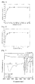
Figure 3 shows results of the ultraviolet spectroscopic measurement on the organic-inorganic hybrid thin film and 4-mercapto phenol prepared in one example of the present invention. -
Figure 4 shows results of the UV-Vis absorption measurement on the organic-inorganic hybrid thin film prepared in one example of the present invention. -
Figure 5 shows results of the air stability test on the organic-inorganic hybrid thin film prepared in one example of the present invention and the thin film prepared in the comparative example. -
Figure 6 shows results of the thin film thickness measurement versus the cycle of the organic-inorganic hybrid thin film formation process in one example of the present invention. -
Figure 7 shows results of the surface roughness measurement on the hybrid thin film prepared in one example of the present invention. -
Figure 8 and Figure 9 respectively show thin film growth rates versus the injection amounts of first precursor and second precursor in one example of the present invention. -
Figure 10 shows results of the ultraviolet spectroscopic measurement on the organic-inorganic hybrid thin film prepared in one example of the present invention. -
Figure 11 shows results of the UV-Vis absorption measurement on the organic-inorganic hybrid thin film prepared in one example of the present invention. -
Figure 12 shows results of the air stability test on the organic-inorganic hybrid thin film prepared in one example of the present invention and the thin film prepared in the comparative example. -
Figure 13 shows results of the thin film thickness measurement of the organic-inorganic hybrid thin film formation process in one example of the present invention. -
Figure 14 shows results of the surface roughness measurement on the hybrid thin film prepared in one example of the present invention. -
Figure 15 shows results of the TEM photograph measurement on the organic-inorganic hybrid super-lattice thin film prepared in one example of the present invention. -
Figure 16 and Figure 17 show the rate of pinhole formation inhibition measured by varying the thickness of an organic-inorganic hybrid thin film in the organic-inorganic hybrid super-lattice thin film prepared in one example of the present invention. -
Figure 18 shows results of the thin film stress measurement versus the ratio of the Al2O3 thin film formed by atomic layer deposition to the organic-inorganic hybrid thin film in the organic-inorganic hybrid super-lattice thin film prepared in one example of the present invention. -
Figure 19 shows results of the Ca test on the organic-inorganic hybrid thin film prepared in one example of the present invention and the thin film prepared in the comparative example. - The present invention is described in further detail below according to examples of the present invention. However, the present invention is not limited to the examples below.
- After an Si (100) substrate was washed with distilled water and acetone, it was purged with N2 gas 2 - 3 times to remove any contaminants on the substrate surface before diethyl zinc (DEZn) was used as a first precursor compound to deposit a diethyl zinc (DEZn) thin film over the Si substrate according to the molecular layer deposition method.
- Over the diethyl zinc (DEZn) thin film was formed an organic molecular film by using 4-mercapto phenol as a second precursor compound according to the molecular layer deposition method to prepare an organic-inorganic hybrid thin film. Argon was used for both carrier gas and purging gas, and DEZn and 4-mercapto phenol were respectively evaporated at 20°C and 70°C. One cycle was achieved by exposure to DEZn for 2 seconds, purging with Ar for 10 seconds, exposure to 4-mercapto phenol for 2 seconds and purging with Ar for 50 seconds. The thin film was grown at a temperature of 80°C to 200°C and under a pressure of 300 mTorr.
- In Example 1, growth rates of the thin film according to the injection time of the first precursor compound of diethyl zinc (DEZn) and growth rates of the thin film according to the injection time of the second precursor compound of 4-mercapto phenol were measured and respectively shown in
Figure 1 and Figure 2 . - It may be noted from
Figure 1 and Figure 2 that growth rates of the thin films increased with injection amounts of the first precursor compound of diethyl zinc (DEZn) and the second precursor compound of 4-mercapto phenol and then the growth rates no longer increased but remained at certain rates. - IR spectroscopic measurements were made on the organic-inorganic hybrid thin film prepared by the same method as Example 1 except that KBr pellets were used instead of the Si substrate and 4-mercapto phenol, and the results are shown in
Figure 3 . - It may be verified in
Figure 3 that a hydroxyl group and a thiol group of 4-mercapto phenol are found in the comparative example in which only 4-mercapto phenol is included whereas in the case of the organic-inorganic hybrid thin film according to the present invention, the hydroxyl group and the thiol group of mercapto phenol used as its second precursor react with the inorganic molecular layer prepared by its first precursor to form a hybrid thin film so that the hydroxyl group and thiol group of mercapto phenol are not detected by the infrared spectroscopic method. - UV-Vis absorption on the organic-inorganic hybrid thin film prepared in Example 1 above was measured and the results are shown in
Figure 4 . - It may be verified from
Figure 4 that the organic-inorganic hybrid thin film according to the present invention has no absorption in the visible ray range. - In a comparative example an organic-inorganic hybrid thin film was prepared the same way as in Example 1 above except that diethyl zinc (DEZn) was used as its first precursor compound to deposit a diethyl zinc (DEZn) thin film oven an Si substrate according to the molecular layer deposition method and then hydroquinone (HQ) was used as its second precursor compound.
- While the organic-inorganic hybrid thin film of Example 1 and the organic-inorganic hybrid thin film prepared in the Comparative Example above were left in air, changes in their thicknesses were measured to test stability in air, and the results are shown in
Figure 5 . - It may be realized in
Figure 5 that unlike in the present invention the thickness drastically decreases in the case of the Comparative Example that does not include an S group whereas the thickness does not change with time in the case of the Example according to the present invention and that the organic-inorganic hybrid multi-layered film including an S group is very stable in air. - As in Example 1 above, diethyl zinc (DEZn) was used as the first precursor compound to deposit a thin film over an Si substrate and 4-mercapto phenol was used as the second precursor compound to form an organic-inorganic hybrid thin film over the diethyl zinc (DEZn) thin film according to the molecular layer deposition method before the process of forming the diethyl zinc (DEZn) by the first precursor compound, and while the thin film based on the second precursor compound was repeatedly formed, thicknesses of the thin film were measured and the results are shown in
Figure 6 . - It may be verified in
Figure 6 that the number of repetitions for the process of forming the thin film by the first precursor compound and forming the thin film by the second precursor compound is proportional to the thickness of the thin film formed. - The organic-inorganic hybrid thin film of 50 nm in the thickness prepared in Example 2 was measured for its surface roughness with AFM, and the results are shown in
Figure 7 . The average roughness measured was 2.2 A. - After an Si (100) substrate was washed with distilled water and acetone, it was purged with N2 gas 2 - 3 times to remove any contaminants on the substrate surface before trimethyl aluminium (TMA) was used as a first precursor compound to deposit a trimethyl aluminium (TMA) thin film over the Si substrate according to the molecular layer deposition method.
- Over the trimethyl aluminium (TMA) thin film was formed an organic molecular film by using 4-mercapto phenol as a second precursor compound according to the molecular layer deposition method to prepare an organic-inorganic hybrid thin film.
- Argon was used for both carrier gas and purging gas, and DEZn and 4-mercapto phenol were respectively evaporated at 20°C and 70°C. One cycle was achieved by exposure to DEZn for 2 seconds, purging with Ar for 10 seconds, exposure to 4-mercapto phenol for 2 seconds and purging with Ar for 50 seconds. The thin film was grown at the temperature of 80°C to 200°C and under a pressure of 300 mTorr.
- In Example 3, growth rates of the thin film according to the injection time of the first precursor compound of trimethyl aluminium (TMA) and growth rates of the thin film according to the injection time of the second precursor compound of 4-mercapto phenol were measured and respectively shown in
Figure 8 and Figure 9 . - It may be noted from
Figure 8 and Figure 9 that growth rates of the thin films increased with injection amounts of the first precursor compound of trimethyl aluminium (TMA) and the second precursor compound of 4-mercapto phenol and then the growth rates no longer increased but remained at certain rates. - IR spectroscopic measurements were made on the organic-inorganic hybrid thin film prepared by the same method of Example 3 except that KBr pellets were used instead of the Si substrate and 4-mercapto phenol, and the results are shown in
Figure 10 . - It may be verified in
Figure 10 that in the case of the organic-inorganic hybrid thin film according to the present invention, the hydroxyl group and the thiol group of mercapto phenol used as its second precursor react with the inorganic molecular layer prepared by its first precursor to form a hybrid thin film so that the hydroxyl group and the thiol group of mercapto phenol are not detected by the infrared spectroscopic method. - UV-Vis absorption on the organic-inorganic hybrid thin film prepared in Example 3 above was measured and the results are shown in
Figure 11 . - It may be verified from
Figure 11 that the organic-inorganic hybrid thin film according to the present invention has no absorption in the visible ray range. - In a comparative example an organic-inorganic hybrid thin film was prepared in the same way as in Example 3 above except that trimethyl aluminium (TMA) was used as its first precursor compound to deposit a trimethyl aluminium (TMA) thin film oven an Si substrate according to the molecular layer deposition method and then hydroquinone (HQ) was used as its second precursor compound.
- While the organic-inorganic hybrid thin film of Example 3 and the organic-inorganic hybrid thin film prepared in the Comparative Example above were left in air, changes in their thicknesses were measured to test stability in air, and the results are shown in
Figure 12 . - It may be recognized in
Figure 12 that, assuming that the initial thickness is d0 and the thickness in n hours is dn, dn/d0 in the case of the Comparative Example without including the S group increases to 0.5 or more as a result of a drastic decrease in its thickness unlike in the present invention whereas in the case of the Example according to the present invention, dn/d0 is kept at 0.1 or less as a result of the absence of changes in its thickness with time and that the organic-inorganic hybrid thin film according to the present invention is very stable in air. - As in Example 3 above, trimethyl aluminium (TMA) was used as the first precursor compound to deposit a thin film over an Si substrate and 4-mercapto phenol was used as the second precursor compound to form an organic-inorganic hybrid thin film over the trimethyl aluminium (TMA) thin film according to the molecular layer deposition method before the process of forming the trimethyl aluminium (TMA) thin film by the first precursor compound, and while the thin film based on the second precursor compound was repeatedly formed, thicknesses of the thin film were measured and the results are shown in
Figure 13 . - It may be verified in
Figure 13 that the number of repetitions for the process of forming the thin film by the first precursor compound and forming the thin film by the second precursor compound is proportional to the thickness of the thin film formed. - The organic-inorganic hybrid thin film of 50 nm in the thickness prepared in Example 4 was measured for its surface roughness with AFM, and the results are shown in
Figure 14 . The average roughness measured was 2.8 A. - After an organic-inorganic hybrid thin film was prepared in the same way as in Examples 1 and 3 above, an Al2O3 thin film was deposited over the organic-inorganic hybrid thin film according to the atomic layer deposition method, and such a process was repeated by controlling the ratio of the Al2O3 thin film based on atomic layer deposition to the organic-inorganic hybrid thin film according to the present invention to prepare an organic-inorganic hybrid functional thin film.
- In order to form the Al2O3 thin film according to atomic layer deposition, argon gas was used as carrier gas and purging gas, and trimethyl aluminium (TMA) and H2O were evaporated at normal temperature. Its cycle was achieved by exposure to TMA for 1 second, purging with Ar for 5 seconds, exposure to H2O for 1 second and purging with Ar for 5 seconds. The above thin film was grown at a temperature of 80°C under a pressure of 300 mTorr.
- The TEM photograph was measured when the ratio of the organic-inorganic hybrid thin film:Al2O3 thin film prepared in Example 5 above was 1:2, and the results are shown in
Figure 15 . It may be verified inFigure 15 that the Al2O3 thin film according to atomic layer deposition and the organic-inorganic hybrid thin film according to the present invention were alternately formed. - In Example 5 above, rates of pinhole formation inhibition were measured by varying the thickness of the organic-inorganic hybrid thin film, and the results are shown in
Figure 16 and Figure 17 . - It may be realized in
Figure 16 that pinholes are seldom formed if the thickness of the organic-inorganic hybrid thin film according to the present invention is 80 nm or more. - In the organic-inorganic hybrid functional thin film prepared in Example 5 above, thin film stress was measured versus the ratio of the Al2O3 thin film to the organic-inorganic hybrid thin film according to the present invention while the total thickness of the thin film was kept the same, and the results are shown in
Figure 18 . - The organic-inorganic hybrid functional thin film prepared in Example 5 above, and the Al2O3 thin film of the Comparative Example were measured for their moisture permeability resistance and oxygen permeability resistance, and the results are listed in Table 1 and
Figure 19 below. - It may be noted from Table 1 and
Figure 19 below that the functional thin film comprising the organic-inorganic hybrid thin film and Al2O3 according to the present invention has superior moisture permeation resistance and oxygen permeation resistance to those of the Comparative Example.[Table 1] Barrier Film WVTR OTR (nm) (g/m2 day) (cm3/m2 day) Al2O3 3.11×10⁻⁷ 9.66×10⁻⁶ (100 nm) Organic/Al2O3 superlattice 2.68×10⁻⁷ 8.33×10⁻⁵ (100nm) - Because the organic-inorganic hybrid thin film and encapsulting film according to the present invention include a new functional group so as to remain stable in air, they can be applied to various fields including nanos patterning for manufacturing semiconductors and electronic devices, chemical sensors and biosensors, nano tribology, surface modification, nano electronic machine systems (NEMS), micro electronic machine systems (MEMS) and non-volatile memory.
- The method for preparing the organic-inorganic hybrid thin film according to the present invention enables provision of a very stable organic-inorganic hybrid multi-layered molecular film in air by including a new functional group not used previously in its organic precursor when preparing the organic-inorganic hybrid thin film by alternately using inorganic precursor and organic precursor according to the molecular layer deposition method.
Claims (17)
- An organic-inorganic hybrid thin film expressed in Formula 1 below:
[Formula 1] -[M-X-R1-Y-]m-
(In the formula 1 above m is 1 or more,R1 is substituted or unsubstituted C1∼20 alkyl, C5∼20 cycloalkyl, or aryl or heteroaryl of 5 ∼ 60 nuclear atoms,M is selected from a group consisting of Zn, Sn, In, Cd, Ga, Al, Ti, Si, V, Mn, Fe, Co, Cu, Zr, Ru, Mo, Nb and W, andX or Y is selected from a group consisting of 0, S, N, NH and CO, and either X or Y is S.) - The organic-inorganic hybrid thin film recited in Claim 1 wherein the thickness of the organic-inorganic hybrid thin film ranges from 1 A to 500 A.
- The organic-inorganic hybrid thin film recited in Claim 1 wherein assuming that the initial thickness of the organic-inorganic hybrid thin film is d0 and that the thickness of the organic-inorganic hybrid thin film after standing under the STP conditions for n hours is dn, the relation equation below is satisfied:

- A functional thin film including an organic-inorganic hybrid thin film that comprises the organic-inorganic hybrid thin film according to Claim 1; and an oxide layer of a metal selected from a group consisting of Zn, Sn, In, Cd, Ga, Al, Ti, Si, V, Mn, Fe, Co, Cu, Zr, Ru, Mo, Nb and W.
- The functional thin film recited in Claim 3 wherein in the functional thin film comprising the organic-inorganic hybrid thin film, the thickness of its metallic oxide layer ranges from 10 A to 2000 A.
- The functional thin film comprising the organic-inorganic hybrid thin film recited in Claim 6 wherein, assuming that the initial thickness of the functional thin film comprising the organic-inorganic hybrid thin film is D0 and that the thickness of the functional thin film comprising the organic-inorganic hybrid thin film after standing under the STP conditions for n hours is Dn, the relation equation below is satisfied:

- The functional thin film recited in Claim 3 wherein the functional thin film comprising the organic-inorganic hybrid thin film is used for encapsulation.
- A method for preparing the organic-inorganic hybrid thin film according to Claim 1 comprising,(1) a step in which the first precursor compound expressed by the formula 2 below is used to form an inorganic molecular layer; and
[Formula 2] M(R21) (R22) ... (R2n)
(In the Formula 2 above M is selected from a group consisting of Zn, Sn, Cd, Ti, Si, V, Mn, Fe, Co, Cu, Zr, Ru, Mo, Nb, W, In, Ga, Al and Tln is determined according to the oxidation number state of the metal M, andR21 to R2n are each independently C1∼20 alkyl, C1∼20 alkoxide, a chloride group, a hydroxide group, an oxyhydroxide group, a nitrate group, a carbonate group, an acetate group or an oxalate group.)(2) a step in which the second precursor compound expressed by the formula 3 below is reacted with the inorganic molecular layer to form an organic molecular layer over the inorganic molecular layer.
[Formula 3] R3-S-R4-R5
(In the Formula 3 above R3 is hydrogen, COR6, C1∼20 alkyl, C5∼20 cycloalkyl, or aryl or heteroaryl of 5 ~ 60 nuclear atoms,R4 is C1∼20 alkyl, C5~20 cycloalkyl, or aryl or heteroaryl of 5 ∼ 60 nuclear atoms,R5 is one or more species selected from a group consisting of a C1∼20 alkoxy group, an ether group, a carboxylic group, COR6, a thiol group and an amine group, andR6 is one or more species selected from a group consisting of hydrogen, an alkoxy group, an ether group, a carboxylic group, a thiol group, and an amine group.) - The method for preparing an organic-inorganic hybrid thin film recited in Claim 8 wherein the second precursor compound is expressed by the formula 4 below:

- The method for preparing an organic-inorganic hybrid thin film recited in Claim 8 wherein the second precursor compound is expressed by the formula 5 below:

- The method for preparing an organic-inorganic hybrid thin film recited in Claim 8 wherein the second precursor compound is expressed by the formula 6 below:


- The method for preparing an organic-inorganic hybrid thin film recited in Claim 8 wherein it further includes repeatedly performing the Step (1) and Step (2).
- The method for preparing an organic-inorganic hybrid thin film recited in Claim 8 wherein the substrate is selected from a group consisting of glass, silicon and plastic.
- The method for preparing an organic-inorganic hybrid thin film recited in Claim 8 wherein it further includes a step in which an oxide layer is formed over the substrate surface prior to the step (1).
- The method for preparing the functional thin film according to claim 8 comprising an organic-inorganic hybrid thin film according to Claim 3 wherein it further includes a step (3) in which an oxide layer of a metal selected from a group consisting of Zn, Sn, In, Cd, Ga, Al, Ti, Si, V, Mn, Fe, Co, Cu, Zr, Ru, Mo, Nb and W is formed by atomic layer deposition.
- The method for preparing a super-lattice thin film recited in Claim 15 wherein the step (3) is repeatedly performed n2 times (n2 is 1 or more) after each of steps (1) and (2) has repeatedly been performed n1 times (n1 is 1 or more).
- The method for preparing an organic-inorganic hybrid thin film recited in Claim 15 wherein the steps (1) to (3) are repeatedly performed.
Applications Claiming Priority (2)
| Application Number | Priority Date | Filing Date | Title |
|---|---|---|---|
| KR1020130104463 | 2013-08-30 | ||
| PCT/KR2013/009909 WO2015030297A1 (en) | 2013-08-30 | 2013-11-04 | Hybrid organic/inorganic thin films and method of manufacturing same |
Publications (3)
| Publication Number | Publication Date |
|---|---|
| EP3040442A1 true EP3040442A1 (en) | 2016-07-06 |
| EP3040442A4 EP3040442A4 (en) | 2017-04-12 |
| EP3040442B1 EP3040442B1 (en) | 2024-02-14 |
Family
ID=52586830
Family Applications (2)
| Application Number | Title | Priority Date | Filing Date |
|---|---|---|---|
| EP13892196.0A Active EP3040442B1 (en) | 2013-08-30 | 2013-11-04 | Functional thin films comprising an hybrid organic/inorganic thin films and method of manufacturing same |
| EP13892719.9A Active EP3040443B1 (en) | 2013-08-30 | 2013-11-04 | Substrate structure and method of manufacturing same |
Family Applications After (1)
| Application Number | Title | Priority Date | Filing Date |
|---|---|---|---|
| EP13892719.9A Active EP3040443B1 (en) | 2013-08-30 | 2013-11-04 | Substrate structure and method of manufacturing same |
Country Status (12)
| Country | Link |
|---|---|
| US (2) | US10418300B2 (en) |
| EP (2) | EP3040442B1 (en) |
| JP (2) | JP6654753B2 (en) |
| KR (2) | KR20150026746A (en) |
| CN (2) | CN105723011B (en) |
| BR (2) | BR112016004476A2 (en) |
| CA (2) | CA2922615A1 (en) |
| MX (2) | MX389406B (en) |
| RU (2) | RU2670303C2 (en) |
| SG (2) | SG11201600921XA (en) |
| TW (2) | TWI521083B (en) |
| WO (2) | WO2015030297A1 (en) |
Families Citing this family (27)
| Publication number | Priority date | Publication date | Assignee | Title |
|---|---|---|---|---|
| US10418300B2 (en) * | 2013-08-30 | 2019-09-17 | Iucf-Hyu (Industry-University Cooperation Foundation Hanyang University | Substrate structure and method for preparing the same |
| CN105431893B (en) * | 2013-09-30 | 2018-01-26 | 株式会社Lg化学 | Substrate for organic electronic device and manufacturing method thereof |
| RU2695997C2 (en) | 2014-06-12 | 2019-07-30 | БАСФ Коатингс ГмбХ | Method of producing flexible organo-inorganic laminar materials |
| EP3274487A1 (en) * | 2015-03-25 | 2018-01-31 | BASF Coatings GmbH | Process for producing flexible organic-inorganic laminates |
| US20190036077A1 (en) * | 2016-02-18 | 2019-01-31 | Sharp Kabushiki Kaisha | Method for producing organic el display device, and organic el display device |
| KR102586045B1 (en) * | 2016-07-12 | 2023-10-10 | 삼성디스플레이 주식회사 | Display apparatus and manufacturing method thereof |
| US20190040503A1 (en) * | 2017-08-03 | 2019-02-07 | Hrl Laboratories, Llc | Feedstocks for additive manufacturing, and methods of using the same |
| WO2019010696A1 (en) * | 2017-07-14 | 2019-01-17 | General Electric Company | A method of gas-phase molecular layer-by-layer deposition on a microporous support |
| US10673046B2 (en) * | 2018-04-13 | 2020-06-02 | GM Global Technology Operations LLC | Separator for lithium metal based batteries |
| CN112334602B (en) * | 2018-07-05 | 2023-06-30 | 巴斯夫涂料有限公司 | Transparent conductive film |
| KR102224346B1 (en) * | 2019-07-11 | 2021-03-05 | 한양대학교 산학협력단 | Organic-inorganic hybrid layer, organic-inorganic laminate having the layer, organic electroinc device including the laminate as a gas barrier |
| CN110508155B (en) * | 2019-08-21 | 2021-09-03 | 南京大学 | Preparation method of zinc-based inorganic-organic hybrid nano porous separation membrane |
| CN110635044B (en) * | 2019-11-04 | 2021-07-06 | 吉林大学 | Composite encapsulation film for organometallic halide perovskite solar cell and preparation method thereof |
| CN112410763A (en) * | 2020-10-28 | 2021-02-26 | 武汉华星光电半导体显示技术有限公司 | Thin film packaging layer, preparation method thereof and foldable display device |
| TWI824213B (en) * | 2020-12-19 | 2023-12-01 | 逢甲大學 | Flexible transparent conductive composite films and method of manufacturing the same |
| KR102558965B1 (en) * | 2021-03-18 | 2023-07-25 | 한국과학기술연구원 | Stretchable disply device and manufacturing method thereof |
| WO2022233992A1 (en) | 2021-05-06 | 2022-11-10 | Basf Coatings Gmbh | Multilayer barrier film, its manufacture and use in photovoltaic applications |
| KR102682640B1 (en) * | 2021-08-12 | 2024-07-08 | 한양대학교 산학협력단 | Multilayer photoresist having molecular line and method for fabricating the same |
| WO2023018308A1 (en) * | 2021-08-12 | 2023-02-16 | 한양대학교 산학협력단 | Multi-layered molecular film photoresist having molecular line structure and method for manufacturing same |
| KR102796366B1 (en) * | 2022-01-13 | 2025-04-18 | 한양대학교 산학협력단 | Method for fabricating multimolecular-layer photoresist having molecular line |
| CN115124727B (en) * | 2022-07-08 | 2023-07-14 | 中国科学院山西煤炭化学研究所 | A kind of preparation method of MOF film |
| CN117845191A (en) * | 2022-09-30 | 2024-04-09 | 华为技术有限公司 | Composite film and its preparation method and application |
| EP4634272A1 (en) | 2022-12-14 | 2025-10-22 | BASF Coatings GmbH | Multilayer barrier film coated polymeric substrate, its manufacture and use in electronic devices |
| JP2026505347A (en) * | 2023-02-10 | 2026-02-13 | 三星電子株式会社 | Multilayer molecular film photoresist with molecular beam structure crosslinkable by coordination bonds |
| WO2024167351A1 (en) * | 2023-02-10 | 2024-08-15 | 한양대학교 산학협력단 | Positive-type multilayer molecular film photoresist having molecular line structure |
| CN116794116B (en) * | 2023-05-29 | 2026-04-28 | 南京大学 | A thin-film hydrogen sensor based on an inorganic-organic hybrid nanoporous membrane/semiconductor metal oxide and its fabrication method. |
| EP4687175A1 (en) | 2024-07-30 | 2026-02-04 | BASF Coatings GmbH | Multilayer film coated lithium substrate, its manufacture and use in secondary batteries |
Family Cites Families (43)
| Publication number | Priority date | Publication date | Assignee | Title |
|---|---|---|---|---|
| RU2118402C1 (en) * | 1994-05-17 | 1998-08-27 | Виктор Васильевич Дроботенко | Method of preparing metal oxide coatings (variants thereof) |
| JP2002053669A (en) | 2000-06-01 | 2002-02-19 | Osaka Organic Chem Ind Ltd | Multidimensional organic-inorganic composite compound and method for producing the same |
| US6866949B2 (en) | 2002-03-08 | 2005-03-15 | Dai Nippon Printing Co., Ltd. | Substrate film, gas barrier film, and display using the same |
| TW548853B (en) * | 2002-09-13 | 2003-08-21 | Ind Tech Res Inst | Method of manufacturing flexible TFT display |
| US7285440B2 (en) * | 2002-11-25 | 2007-10-23 | International Business Machines Corporation | Organic underlayers that improve the performance of organic semiconductors |
| JP2004231784A (en) * | 2003-01-30 | 2004-08-19 | Konica Minolta Holdings Inc | Organic-inorganic polymer hybrid film, its preparation method, and display and touch panel using said film |
| US7229703B2 (en) | 2003-03-31 | 2007-06-12 | Dai Nippon Printing Co. Ltd. | Gas barrier substrate |
| JP4654911B2 (en) | 2003-05-16 | 2011-03-23 | 凸版印刷株式会社 | Transparent gas barrier laminated film, electroluminescence light emitting device, electroluminescence display device, and electrophoretic display panel using the same |
| WO2005056354A2 (en) | 2003-12-03 | 2005-06-23 | Gedeon Anthony A | Method of resisting contaminant build up and oxidation of vehicle surfaces and other surfaces |
| JP2005289885A (en) | 2004-03-31 | 2005-10-20 | Osaka Organic Chem Ind Ltd | Multi-dimensional organic / inorganic composite compound, composite fired body, and production method thereof |
| JP2005297498A (en) | 2004-04-16 | 2005-10-27 | Dainippon Printing Co Ltd | Flexible substrate and organic device using the same |
| US7378157B2 (en) | 2004-06-28 | 2008-05-27 | Dai Nippon Printing Co., Ltd. | Gas barrier film, and display substrate and display using the same |
| KR101001441B1 (en) * | 2004-08-17 | 2010-12-14 | 삼성전자주식회사 | Organic-inorganic metal hybrid material and organic insulator composition comprising same |
| NO20045674D0 (en) * | 2004-12-28 | 2004-12-28 | Uni I Oslo | Thin films prepared with gas phase deposition technique |
| JP2007185937A (en) | 2005-12-12 | 2007-07-26 | Fujifilm Corp | Organic-inorganic hybrid material, gas barrier film and method for producing the same |
| KR20070084683A (en) * | 2006-02-21 | 2007-08-27 | 국민대학교산학협력단 | Molecular Layer Deposition |
| JP2007273094A (en) | 2006-03-30 | 2007-10-18 | Toppan Printing Co Ltd | Organic electroluminescence device and method for manufacturing the same |
| DE102006016280A1 (en) * | 2006-04-01 | 2007-10-04 | Pvflex Solar Gmbh | Glassless thin-film solar power module, has solar cell in starting, inorganic barrier layer, inorganic-organic hybrid polymer barrier layer, transparent adhesive layer and cover film in front side and adhesive layer in rear side |
| JP2008087163A (en) | 2006-09-29 | 2008-04-17 | Fujifilm Corp | Gas barrier laminate film and image display element using the same |
| KR101449076B1 (en) | 2006-11-13 | 2015-02-23 | 더 리젠츠 오브 더 유니버시티 오브 콜로라도, 어 바디 코포레이트 | Molecular layer deposition process for the production of organic or organic-inorganic polymers |
| JP2008218632A (en) * | 2007-03-02 | 2008-09-18 | Fujifilm Corp | Electronic devices |
| US8197942B2 (en) | 2007-03-23 | 2012-06-12 | Dai Nippon Printing Co., Ltd. | Gas barrier sheet |
| JP5127277B2 (en) | 2007-04-05 | 2013-01-23 | 新日鉄住金マテリアルズ株式会社 | Surface flatness insulating film forming coating solution, surface flatness insulating film coated base material, and method for producing surface flatness insulating film coated base material |
| JP5198131B2 (en) | 2007-05-14 | 2013-05-15 | 富士フイルム株式会社 | Barrier film and element |
| US7947377B2 (en) | 2007-06-20 | 2011-05-24 | Dai Nippon Printing Co., Ltd. | Powder mixture to be made into evaporation source material for use in ion plating, evaporation source material for use in ion plating and method of producing the same, and gas barrier sheet and method of producing the same |
| US9660205B2 (en) | 2007-06-22 | 2017-05-23 | Regents Of The University Of Colorado | Protective coatings for organic electronic devices made using atomic layer deposition and molecular layer deposition techniques |
| US20090021797A1 (en) * | 2007-07-17 | 2009-01-22 | Luciano Joseph W | All-In-One Device With Integrated Monitor |
| JP2010006039A (en) | 2007-09-05 | 2010-01-14 | Fujifilm Corp | Gas barrier film, and method for sealing display element using gas barrier film |
| US8067085B2 (en) | 2007-09-14 | 2011-11-29 | Fujifilm Corporation | Gas barrier film, and display device comprising the same |
| US7858144B2 (en) * | 2007-09-26 | 2010-12-28 | Eastman Kodak Company | Process for depositing organic materials |
| RU2462793C2 (en) * | 2007-12-28 | 2012-09-27 | Юниверсите Де Ля Медитерране Экс-Марсель Ii | Hybrid nanocomposite materials |
| US8776238B2 (en) * | 2008-07-16 | 2014-07-08 | International Business Machines Corporation | Verifying certificate use |
| US8241749B2 (en) | 2008-09-11 | 2012-08-14 | Fujifilm Corporation | Barrier laminate, gas barrier film, and device using the same |
| JP2011046060A (en) | 2009-08-26 | 2011-03-10 | Fujifilm Corp | Gas barrier film and method for manufacturing gas barrier film |
| JP4821925B2 (en) | 2009-11-27 | 2011-11-24 | 大日本印刷株式会社 | GAS BARRIER FILM, DEVICE, AND METHOD FOR PRODUCING GAS BARRIER FILM |
| US9306186B2 (en) | 2010-03-17 | 2016-04-05 | Konica Minolta, Inc. | Organic electronic device and method of manufacturing the same |
| KR101886880B1 (en) | 2010-03-25 | 2018-08-08 | 도판 인사츠 가부시키가이샤 | Gas barrier laminate and packaging material |
| JP5598080B2 (en) | 2010-05-17 | 2014-10-01 | 大日本印刷株式会社 | Method for producing gas barrier sheet |
| JP5913809B2 (en) | 2011-01-05 | 2016-04-27 | リンテック株式会社 | Transparent electrode substrate, method for producing the same, electronic device having the transparent electrode substrate, and solar cell |
| JP5752438B2 (en) * | 2011-02-23 | 2015-07-22 | グンゼ株式会社 | Gas barrier film |
| KR101367956B1 (en) * | 2011-05-16 | 2014-02-26 | 주식회사 엘지화학 | Multilayer plastic substrate and method for manufacturing same |
| KR101432737B1 (en) | 2011-07-28 | 2014-08-22 | 한양대학교 산학협력단 | Hybrid organic-inorganic thin film and producing method of the same |
| US10418300B2 (en) * | 2013-08-30 | 2019-09-17 | Iucf-Hyu (Industry-University Cooperation Foundation Hanyang University | Substrate structure and method for preparing the same |
-
2013
- 2013-11-04 US US14/915,562 patent/US10418300B2/en active Active
- 2013-11-04 CN CN201380079150.XA patent/CN105723011B/en active Active
- 2013-11-04 CA CA2922615A patent/CA2922615A1/en not_active Abandoned
- 2013-11-04 WO PCT/KR2013/009909 patent/WO2015030297A1/en not_active Ceased
- 2013-11-04 JP JP2016538483A patent/JP6654753B2/en active Active
- 2013-11-04 EP EP13892196.0A patent/EP3040442B1/en active Active
- 2013-11-04 BR BR112016004476A patent/BR112016004476A2/en not_active Application Discontinuation
- 2013-11-04 WO PCT/KR2013/009910 patent/WO2015030298A1/en not_active Ceased
- 2013-11-04 BR BR112016004389-8A patent/BR112016004389B1/en active IP Right Grant
- 2013-11-04 SG SG11201600921XA patent/SG11201600921XA/en unknown
- 2013-11-04 JP JP2016538482A patent/JP6286557B2/en active Active
- 2013-11-04 CN CN201380079249.XA patent/CN105745353B/en active Active
- 2013-11-04 CA CA2922612A patent/CA2922612A1/en not_active Abandoned
- 2013-11-04 RU RU2016111693A patent/RU2670303C2/en active
- 2013-11-04 RU RU2016111694A patent/RU2672962C2/en active
- 2013-11-04 MX MX2016002432A patent/MX389406B/en unknown
- 2013-11-04 SG SG11201600923YA patent/SG11201600923YA/en unknown
- 2013-11-04 MX MX2016002433A patent/MX390737B/en unknown
- 2013-11-04 EP EP13892719.9A patent/EP3040443B1/en active Active
- 2013-11-04 US US14/413,754 patent/US9576876B2/en active Active
- 2013-12-02 TW TW102144000A patent/TWI521083B/en active
- 2013-12-02 TW TW102143967A patent/TWI606111B/en active
-
2014
- 2014-02-17 KR KR20140018154A patent/KR20150026746A/en not_active Withdrawn
- 2014-02-18 KR KR1020140018212A patent/KR102289064B1/en active Active
Also Published As
Similar Documents
| Publication | Publication Date | Title |
|---|---|---|
| US9576876B2 (en) | Organic-inorganic hybrid thin film and method for producing the same | |
| US12365981B2 (en) | Synthesis and use of precursors for ALD of molybdenum or tungsten containing thin films | |
| Malm et al. | Atomic layer deposition of WO3 thin films using W (CO) 6 and O3 precursors | |
| Pore et al. | Atomic layer deposition of antimony and its compounds using dechlorosilylation reactions of tris (triethylsilyl) antimony | |
| US20190112716A1 (en) | A method for etching a metal surface | |
| Cloud et al. | Low-temperature CVD of iron, cobalt, and nickel nitride thin films from bis [di (tert-butyl) amido] metal (II) precursors and ammonia | |
| Salles et al. | Chemical synthesis of complex oxide thin films and freestanding membranes | |
| KR20150026747A (en) | Organic inorganic hybrid thin films and method for preparing the same | |
| Scott et al. | Versatile method for template-free synthesis of single crystalline metal and metal alloy nanowires | |
| US12252784B2 (en) | Copper halide layers | |
| WO2008111850A2 (en) | Synthesis of molecular metalorganic compounds | |
| KR102139285B1 (en) | Organometallic precursor compound for vapor deposition for forming oxide thin film and method for manufacturing same | |
| KR100643637B1 (en) | Process for preparing nickel oxide thin film by atomic layer deposition using nickel aminoalkoxide precursor | |
| KR100416504B1 (en) | Manganese-doped ferromagnetic zinc oxide and method of manufacturing the same | |
| US20130337157A1 (en) | Method for synthesizing metal or metal oxide nanoparticles by liquid phase deposition on the surface of a substrate | |
| Barreca | Malonate complexes of dysprosium: synthesis, characterization and application for LI-MOCVD of dysprosium containing thin films |
Legal Events
| Date | Code | Title | Description |
|---|---|---|---|
| PUAI | Public reference made under article 153(3) epc to a published international application that has entered the european phase |
Free format text: ORIGINAL CODE: 0009012 |
|
| 17P | Request for examination filed |
Effective date: 20160330 |
|
| AK | Designated contracting states |
Kind code of ref document: A1 Designated state(s): AL AT BE BG CH CY CZ DE DK EE ES FI FR GB GR HR HU IE IS IT LI LT LU LV MC MK MT NL NO PL PT RO RS SE SI SK SM TR |
|
| AX | Request for extension of the european patent |
Extension state: BA ME |
|
| DAX | Request for extension of the european patent (deleted) | ||
| A4 | Supplementary search report drawn up and despatched |
Effective date: 20170313 |
|
| RIC1 | Information provided on ipc code assigned before grant |
Ipc: C23C 16/00 20060101AFI20170307BHEP Ipc: C23C 16/448 20060101ALI20170307BHEP |
|
| STAA | Information on the status of an ep patent application or granted ep patent |
Free format text: STATUS: EXAMINATION IS IN PROGRESS |
|
| 17Q | First examination report despatched |
Effective date: 20170918 |
|
| RAP1 | Party data changed (applicant data changed or rights of an application transferred) |
Owner name: IUCF-HYU (INDUSTRY-UNIVERSITY COOPERATION FOUNDATION HANYANG UNIVERSITY) |
|
| GRAP | Despatch of communication of intention to grant a patent |
Free format text: ORIGINAL CODE: EPIDOSNIGR1 |
|
| STAA | Information on the status of an ep patent application or granted ep patent |
Free format text: STATUS: GRANT OF PATENT IS INTENDED |
|
| INTG | Intention to grant announced |
Effective date: 20231013 |
|
| GRAS | Grant fee paid |
Free format text: ORIGINAL CODE: EPIDOSNIGR3 |
|
| GRAA | (expected) grant |
Free format text: ORIGINAL CODE: 0009210 |
|
| STAA | Information on the status of an ep patent application or granted ep patent |
Free format text: STATUS: THE PATENT HAS BEEN GRANTED |
|
| AK | Designated contracting states |
Kind code of ref document: B1 Designated state(s): AL AT BE BG CH CY CZ DE DK EE ES FI FR GB GR HR HU IE IS IT LI LT LU LV MC MK MT NL NO PL PT RO RS SE SI SK SM TR |
|
| REG | Reference to a national code |
Ref country code: GB Ref legal event code: FG4D |
|
| REG | Reference to a national code |
Ref country code: CH Ref legal event code: EP |
|
| REG | Reference to a national code |
Ref country code: DE Ref legal event code: R096 Ref document number: 602013085299 Country of ref document: DE |
|
| REG | Reference to a national code |
Ref country code: IE Ref legal event code: FG4D |
|
| REG | Reference to a national code |
Ref country code: LT Ref legal event code: MG9D |
|
| REG | Reference to a national code |
Ref country code: NL Ref legal event code: MP Effective date: 20240214 |
|
| PG25 | Lapsed in a contracting state [announced via postgrant information from national office to epo] |
Ref country code: IS Free format text: LAPSE BECAUSE OF FAILURE TO SUBMIT A TRANSLATION OF THE DESCRIPTION OR TO PAY THE FEE WITHIN THE PRESCRIBED TIME-LIMIT Effective date: 20240614 |
|
| PG25 | Lapsed in a contracting state [announced via postgrant information from national office to epo] |
Ref country code: LT Free format text: LAPSE BECAUSE OF FAILURE TO SUBMIT A TRANSLATION OF THE DESCRIPTION OR TO PAY THE FEE WITHIN THE PRESCRIBED TIME-LIMIT Effective date: 20240214 |
|
| PG25 | Lapsed in a contracting state [announced via postgrant information from national office to epo] |
Ref country code: GR Free format text: LAPSE BECAUSE OF FAILURE TO SUBMIT A TRANSLATION OF THE DESCRIPTION OR TO PAY THE FEE WITHIN THE PRESCRIBED TIME-LIMIT Effective date: 20240515 |
|
| REG | Reference to a national code |
Ref country code: AT Ref legal event code: MK05 Ref document number: 1657072 Country of ref document: AT Kind code of ref document: T Effective date: 20240214 |
|
| PG25 | Lapsed in a contracting state [announced via postgrant information from national office to epo] |
Ref country code: RS Free format text: LAPSE BECAUSE OF FAILURE TO SUBMIT A TRANSLATION OF THE DESCRIPTION OR TO PAY THE FEE WITHIN THE PRESCRIBED TIME-LIMIT Effective date: 20240514 Ref country code: NL Free format text: LAPSE BECAUSE OF FAILURE TO SUBMIT A TRANSLATION OF THE DESCRIPTION OR TO PAY THE FEE WITHIN THE PRESCRIBED TIME-LIMIT Effective date: 20240214 Ref country code: HR Free format text: LAPSE BECAUSE OF FAILURE TO SUBMIT A TRANSLATION OF THE DESCRIPTION OR TO PAY THE FEE WITHIN THE PRESCRIBED TIME-LIMIT Effective date: 20240214 |
|
| PG25 | Lapsed in a contracting state [announced via postgrant information from national office to epo] |
Ref country code: ES Free format text: LAPSE BECAUSE OF FAILURE TO SUBMIT A TRANSLATION OF THE DESCRIPTION OR TO PAY THE FEE WITHIN THE PRESCRIBED TIME-LIMIT Effective date: 20240214 |
|
| PG25 | Lapsed in a contracting state [announced via postgrant information from national office to epo] |
Ref country code: AT Free format text: LAPSE BECAUSE OF FAILURE TO SUBMIT A TRANSLATION OF THE DESCRIPTION OR TO PAY THE FEE WITHIN THE PRESCRIBED TIME-LIMIT Effective date: 20240214 |
|
| PG25 | Lapsed in a contracting state [announced via postgrant information from national office to epo] |
Ref country code: RS Free format text: LAPSE BECAUSE OF FAILURE TO SUBMIT A TRANSLATION OF THE DESCRIPTION OR TO PAY THE FEE WITHIN THE PRESCRIBED TIME-LIMIT Effective date: 20240514 Ref country code: NO Free format text: LAPSE BECAUSE OF FAILURE TO SUBMIT A TRANSLATION OF THE DESCRIPTION OR TO PAY THE FEE WITHIN THE PRESCRIBED TIME-LIMIT Effective date: 20240514 Ref country code: NL Free format text: LAPSE BECAUSE OF FAILURE TO SUBMIT A TRANSLATION OF THE DESCRIPTION OR TO PAY THE FEE WITHIN THE PRESCRIBED TIME-LIMIT Effective date: 20240214 Ref country code: LT Free format text: LAPSE BECAUSE OF FAILURE TO SUBMIT A TRANSLATION OF THE DESCRIPTION OR TO PAY THE FEE WITHIN THE PRESCRIBED TIME-LIMIT Effective date: 20240214 Ref country code: IS Free format text: LAPSE BECAUSE OF FAILURE TO SUBMIT A TRANSLATION OF THE DESCRIPTION OR TO PAY THE FEE WITHIN THE PRESCRIBED TIME-LIMIT Effective date: 20240614 Ref country code: HR Free format text: LAPSE BECAUSE OF FAILURE TO SUBMIT A TRANSLATION OF THE DESCRIPTION OR TO PAY THE FEE WITHIN THE PRESCRIBED TIME-LIMIT Effective date: 20240214 Ref country code: GR Free format text: LAPSE BECAUSE OF FAILURE TO SUBMIT A TRANSLATION OF THE DESCRIPTION OR TO PAY THE FEE WITHIN THE PRESCRIBED TIME-LIMIT Effective date: 20240515 Ref country code: FI Free format text: LAPSE BECAUSE OF FAILURE TO SUBMIT A TRANSLATION OF THE DESCRIPTION OR TO PAY THE FEE WITHIN THE PRESCRIBED TIME-LIMIT Effective date: 20240214 Ref country code: ES Free format text: LAPSE BECAUSE OF FAILURE TO SUBMIT A TRANSLATION OF THE DESCRIPTION OR TO PAY THE FEE WITHIN THE PRESCRIBED TIME-LIMIT Effective date: 20240214 Ref country code: BG Free format text: LAPSE BECAUSE OF FAILURE TO SUBMIT A TRANSLATION OF THE DESCRIPTION OR TO PAY THE FEE WITHIN THE PRESCRIBED TIME-LIMIT Effective date: 20240214 Ref country code: AT Free format text: LAPSE BECAUSE OF FAILURE TO SUBMIT A TRANSLATION OF THE DESCRIPTION OR TO PAY THE FEE WITHIN THE PRESCRIBED TIME-LIMIT Effective date: 20240214 |
|
| PG25 | Lapsed in a contracting state [announced via postgrant information from national office to epo] |
Ref country code: PT Free format text: LAPSE BECAUSE OF FAILURE TO SUBMIT A TRANSLATION OF THE DESCRIPTION OR TO PAY THE FEE WITHIN THE PRESCRIBED TIME-LIMIT Effective date: 20240614 Ref country code: PL Free format text: LAPSE BECAUSE OF FAILURE TO SUBMIT A TRANSLATION OF THE DESCRIPTION OR TO PAY THE FEE WITHIN THE PRESCRIBED TIME-LIMIT Effective date: 20240214 |
|
| PG25 | Lapsed in a contracting state [announced via postgrant information from national office to epo] |
Ref country code: SE Free format text: LAPSE BECAUSE OF FAILURE TO SUBMIT A TRANSLATION OF THE DESCRIPTION OR TO PAY THE FEE WITHIN THE PRESCRIBED TIME-LIMIT Effective date: 20240214 Ref country code: PT Free format text: LAPSE BECAUSE OF FAILURE TO SUBMIT A TRANSLATION OF THE DESCRIPTION OR TO PAY THE FEE WITHIN THE PRESCRIBED TIME-LIMIT Effective date: 20240614 Ref country code: PL Free format text: LAPSE BECAUSE OF FAILURE TO SUBMIT A TRANSLATION OF THE DESCRIPTION OR TO PAY THE FEE WITHIN THE PRESCRIBED TIME-LIMIT Effective date: 20240214 Ref country code: LV Free format text: LAPSE BECAUSE OF FAILURE TO SUBMIT A TRANSLATION OF THE DESCRIPTION OR TO PAY THE FEE WITHIN THE PRESCRIBED TIME-LIMIT Effective date: 20240214 |
|
| PG25 | Lapsed in a contracting state [announced via postgrant information from national office to epo] |
Ref country code: DK Free format text: LAPSE BECAUSE OF FAILURE TO SUBMIT A TRANSLATION OF THE DESCRIPTION OR TO PAY THE FEE WITHIN THE PRESCRIBED TIME-LIMIT Effective date: 20240214 |
|
| PG25 | Lapsed in a contracting state [announced via postgrant information from national office to epo] |
Ref country code: SM Free format text: LAPSE BECAUSE OF FAILURE TO SUBMIT A TRANSLATION OF THE DESCRIPTION OR TO PAY THE FEE WITHIN THE PRESCRIBED TIME-LIMIT Effective date: 20240214 |
|
| PG25 | Lapsed in a contracting state [announced via postgrant information from national office to epo] |
Ref country code: CZ Free format text: LAPSE BECAUSE OF FAILURE TO SUBMIT A TRANSLATION OF THE DESCRIPTION OR TO PAY THE FEE WITHIN THE PRESCRIBED TIME-LIMIT Effective date: 20240214 Ref country code: EE Free format text: LAPSE BECAUSE OF FAILURE TO SUBMIT A TRANSLATION OF THE DESCRIPTION OR TO PAY THE FEE WITHIN THE PRESCRIBED TIME-LIMIT Effective date: 20240214 |
|
| PG25 | Lapsed in a contracting state [announced via postgrant information from national office to epo] |
Ref country code: SK Free format text: LAPSE BECAUSE OF FAILURE TO SUBMIT A TRANSLATION OF THE DESCRIPTION OR TO PAY THE FEE WITHIN THE PRESCRIBED TIME-LIMIT Effective date: 20240214 |
|
| PG25 | Lapsed in a contracting state [announced via postgrant information from national office to epo] |
Ref country code: SM Free format text: LAPSE BECAUSE OF FAILURE TO SUBMIT A TRANSLATION OF THE DESCRIPTION OR TO PAY THE FEE WITHIN THE PRESCRIBED TIME-LIMIT Effective date: 20240214 Ref country code: SK Free format text: LAPSE BECAUSE OF FAILURE TO SUBMIT A TRANSLATION OF THE DESCRIPTION OR TO PAY THE FEE WITHIN THE PRESCRIBED TIME-LIMIT Effective date: 20240214 Ref country code: RO Free format text: LAPSE BECAUSE OF FAILURE TO SUBMIT A TRANSLATION OF THE DESCRIPTION OR TO PAY THE FEE WITHIN THE PRESCRIBED TIME-LIMIT Effective date: 20240214 Ref country code: EE Free format text: LAPSE BECAUSE OF FAILURE TO SUBMIT A TRANSLATION OF THE DESCRIPTION OR TO PAY THE FEE WITHIN THE PRESCRIBED TIME-LIMIT Effective date: 20240214 Ref country code: DK Free format text: LAPSE BECAUSE OF FAILURE TO SUBMIT A TRANSLATION OF THE DESCRIPTION OR TO PAY THE FEE WITHIN THE PRESCRIBED TIME-LIMIT Effective date: 20240214 Ref country code: CZ Free format text: LAPSE BECAUSE OF FAILURE TO SUBMIT A TRANSLATION OF THE DESCRIPTION OR TO PAY THE FEE WITHIN THE PRESCRIBED TIME-LIMIT Effective date: 20240214 |
|
| REG | Reference to a national code |
Ref country code: DE Ref legal event code: R097 Ref document number: 602013085299 Country of ref document: DE |
|
| PG25 | Lapsed in a contracting state [announced via postgrant information from national office to epo] |
Ref country code: IT Free format text: LAPSE BECAUSE OF FAILURE TO SUBMIT A TRANSLATION OF THE DESCRIPTION OR TO PAY THE FEE WITHIN THE PRESCRIBED TIME-LIMIT Effective date: 20240214 |
|
| PLBE | No opposition filed within time limit |
Free format text: ORIGINAL CODE: 0009261 |
|
| STAA | Information on the status of an ep patent application or granted ep patent |
Free format text: STATUS: NO OPPOSITION FILED WITHIN TIME LIMIT |
|
| PG25 | Lapsed in a contracting state [announced via postgrant information from national office to epo] |
Ref country code: IT Free format text: LAPSE BECAUSE OF FAILURE TO SUBMIT A TRANSLATION OF THE DESCRIPTION OR TO PAY THE FEE WITHIN THE PRESCRIBED TIME-LIMIT Effective date: 20240214 |
|
| 26N | No opposition filed |
Effective date: 20241115 |
|
| PG25 | Lapsed in a contracting state [announced via postgrant information from national office to epo] |
Ref country code: SI Free format text: LAPSE BECAUSE OF FAILURE TO SUBMIT A TRANSLATION OF THE DESCRIPTION OR TO PAY THE FEE WITHIN THE PRESCRIBED TIME-LIMIT Effective date: 20240214 |
|
| REG | Reference to a national code |
Ref country code: CH Ref legal event code: PL |
|
| PG25 | Lapsed in a contracting state [announced via postgrant information from national office to epo] |
Ref country code: MC Free format text: LAPSE BECAUSE OF FAILURE TO SUBMIT A TRANSLATION OF THE DESCRIPTION OR TO PAY THE FEE WITHIN THE PRESCRIBED TIME-LIMIT Effective date: 20240214 |
|
| PG25 | Lapsed in a contracting state [announced via postgrant information from national office to epo] |
Ref country code: LU Free format text: LAPSE BECAUSE OF NON-PAYMENT OF DUE FEES Effective date: 20241104 |
|
| REG | Reference to a national code |
Ref country code: CH Ref legal event code: PL |
|
| PG25 | Lapsed in a contracting state [announced via postgrant information from national office to epo] |
Ref country code: CH Free format text: LAPSE BECAUSE OF NON-PAYMENT OF DUE FEES Effective date: 20241130 |
|
| REG | Reference to a national code |
Ref country code: BE Ref legal event code: MM Effective date: 20241130 |
|
| PG25 | Lapsed in a contracting state [announced via postgrant information from national office to epo] |
Ref country code: BE Free format text: LAPSE BECAUSE OF NON-PAYMENT OF DUE FEES Effective date: 20241130 |
|
| PGFP | Annual fee paid to national office [announced via postgrant information from national office to epo] |
Ref country code: GB Payment date: 20250922 Year of fee payment: 13 |
|
| PGFP | Annual fee paid to national office [announced via postgrant information from national office to epo] |
Ref country code: FR Payment date: 20250925 Year of fee payment: 13 |
|
| PG25 | Lapsed in a contracting state [announced via postgrant information from national office to epo] |
Ref country code: IE Free format text: LAPSE BECAUSE OF NON-PAYMENT OF DUE FEES Effective date: 20241104 |
|
| PGFP | Annual fee paid to national office [announced via postgrant information from national office to epo] |
Ref country code: DE Payment date: 20250922 Year of fee payment: 13 |
|
| PG25 | Lapsed in a contracting state [announced via postgrant information from national office to epo] |
Ref country code: HU Free format text: LAPSE BECAUSE OF FAILURE TO SUBMIT A TRANSLATION OF THE DESCRIPTION OR TO PAY THE FEE WITHIN THE PRESCRIBED TIME-LIMIT; INVALID AB INITIO Effective date: 20131104 |
|
| PG25 | Lapsed in a contracting state [announced via postgrant information from national office to epo] |
Ref country code: CY Free format text: LAPSE BECAUSE OF FAILURE TO SUBMIT A TRANSLATION OF THE DESCRIPTION OR TO PAY THE FEE WITHIN THE PRESCRIBED TIME-LIMIT; INVALID AB INITIO Effective date: 20131104 |