EP3035536A1 - An ADPLL having a TDC circuit with a dynamically adjustable offset delay - Google Patents
An ADPLL having a TDC circuit with a dynamically adjustable offset delay Download PDFInfo
- Publication number
- EP3035536A1 EP3035536A1 EP14199426.9A EP14199426A EP3035536A1 EP 3035536 A1 EP3035536 A1 EP 3035536A1 EP 14199426 A EP14199426 A EP 14199426A EP 3035536 A1 EP3035536 A1 EP 3035536A1
- Authority
- EP
- European Patent Office
- Prior art keywords
- tdc
- offset
- delay
- adpll
- observation window
- Prior art date
- Legal status (The legal status is an assumption and is not a legal conclusion. Google has not performed a legal analysis and makes no representation as to the accuracy of the status listed.)
- Granted
Links
Images





Classifications
-
- H—ELECTRICITY
- H03—ELECTRONIC CIRCUITRY
- H03L—AUTOMATIC CONTROL, STARTING, SYNCHRONISATION OR STABILISATION OF GENERATORS OF ELECTRONIC OSCILLATIONS OR PULSES
- H03L7/00—Automatic control of frequency or phase; Synchronisation
- H03L7/06—Automatic control of frequency or phase; Synchronisation using a reference signal applied to a frequency- or phase-locked loop
- H03L7/08—Details of the phase-locked loop
- H03L7/099—Details of the phase-locked loop concerning mainly the controlled oscillator of the loop
- H03L7/0991—Details of the phase-locked loop concerning mainly the controlled oscillator of the loop the oscillator being a digital oscillator, e.g. composed of a fixed oscillator followed by a variable frequency divider
-
- G—PHYSICS
- G04—HOROLOGY
- G04F—TIME-INTERVAL MEASURING
- G04F10/00—Apparatus for measuring unknown time intervals by electric means
- G04F10/005—Time-to-digital converters [TDC]
-
- H—ELECTRICITY
- H03—ELECTRONIC CIRCUITRY
- H03L—AUTOMATIC CONTROL, STARTING, SYNCHRONISATION OR STABILISATION OF GENERATORS OF ELECTRONIC OSCILLATIONS OR PULSES
- H03L7/00—Automatic control of frequency or phase; Synchronisation
- H03L7/06—Automatic control of frequency or phase; Synchronisation using a reference signal applied to a frequency- or phase-locked loop
- H03L7/08—Details of the phase-locked loop
- H03L7/081—Details of the phase-locked loop provided with an additional controlled phase shifter
- H03L7/0812—Details of the phase-locked loop provided with an additional controlled phase shifter and where no voltage or current controlled oscillator is used
- H03L7/0814—Details of the phase-locked loop provided with an additional controlled phase shifter and where no voltage or current controlled oscillator is used the phase shifting device being digitally controlled
-
- H—ELECTRICITY
- H03—ELECTRONIC CIRCUITRY
- H03L—AUTOMATIC CONTROL, STARTING, SYNCHRONISATION OR STABILISATION OF GENERATORS OF ELECTRONIC OSCILLATIONS OR PULSES
- H03L7/00—Automatic control of frequency or phase; Synchronisation
- H03L7/06—Automatic control of frequency or phase; Synchronisation using a reference signal applied to a frequency- or phase-locked loop
- H03L7/08—Details of the phase-locked loop
- H03L7/085—Details of the phase-locked loop concerning mainly the frequency- or phase-detection arrangement including the filtering or amplification of its output signal
- H03L7/091—Details of the phase-locked loop concerning mainly the frequency- or phase-detection arrangement including the filtering or amplification of its output signal the phase or frequency detector using a sampling device
-
- H—ELECTRICITY
- H03—ELECTRONIC CIRCUITRY
- H03L—AUTOMATIC CONTROL, STARTING, SYNCHRONISATION OR STABILISATION OF GENERATORS OF ELECTRONIC OSCILLATIONS OR PULSES
- H03L2207/00—Indexing scheme relating to automatic control of frequency or phase and to synchronisation
- H03L2207/50—All digital phase-locked loop
Definitions
- the present disclosure relates to an All-Digital-Phase-Locked-Loop (ADPLL) and more specifically to an ADPLL having a TDC with a dynamically adjustable offset delay.
- ADPLL All-Digital-Phase-Locked-Loop
- Ultra-low-power (ULP) transceivers enable short-range networks of autonomous sensor nodes for wireless personal area network (WPAN) applications, e.g., Bluetooth Smart and Zigbee.
- WLAN personal area network
- PLL Phase-Locked-Loops
- ADPLLs all-digital PLLs
- ADPLLs are preferred in nanoscale CMOS as they offer benefit from smaller area overhead, programmability, capability of extensive self-calibrations, and easy portability.
- analog PLLs currently still dominate the field of ULP WPAN radios, since the time-to-digital-converter (TDC) of an ADPLL has traditionally been power hungry.
- a known approach for minimising the power consumption of a TDC circuit in the ADPLL is to reduce the activity of the TDC so that it operates only within a predetermined observation window.
- Such a TDC is known from J. Zhuang, et al., "A Low-Power All-Digital PLL Architecture Based on Phase Prediction," ICECS, 2012 , where a 2.1-2.7GHz fractional-N ADPLL for WPAN applications DTC-assisted snapshot TDC is presented.
- TDC snapshotting is implemented to reduce the sampling rate of the TDC from FCKVD2 to FREF.
- a Digital-to-Time Converter is provided for reducing the detection range of the TDC detection range to less than 1/10 of the DCO output signal period, leading to a significant power reduction.
- the accumulated fractional part of the frequency command word, FCW frac controls the DTC to delay the reference signal FREF such that the delayed reference clock FREF dly is almost aligned with CKVD2, once the loop is locked.
- FREF dly also triggers the snapshot to catch the first CKVD2 edge so that only one CKVD2 edge, CKVD2 S , per reference period is fed to the TDC. By capturing only one edge, the snapshot technique guarantees that the TDC has the minimum activity and consume minimum power.
- the snapshotting also minimize the supply switch noise during TDC operation.
- a reduced-range TDC operating at the reference frequency (32MHz) compares the edge of CKVD2 S with FREF dly to provide the fractional phase error, PHE F .
- This approach reduces both sampling speed and detection range of TDC, leading to around 200x power reduction.
- the narrow observation window is opened by the CKVD2 s , which acts as a TDC enable signal, after the rising edge of FREF dly . Since the TDC captures only the first rising edge of the variable clock, CDVD2, after the rising edge of FREF dly , the timing of opening TDC observation window is critical.
- T1 TDC "offset delay"
- T1 TDC "offset delay"
- the TDC and snapshot circuit offset delays cannot be easily estimated due to parasitic or slow logic transitions introduced in the layout during the design phase or during operation.
- the TDC may be activated outside of the predetermined observation window, thereby causing the TDC to generate an erroneous output code, resulting in the degradation of the overall PLL performance, e.g. by introducing unwanted phase noise, and sometimes may even lead to an unstable PLL locking.
- an All-Digital-Phase-Locked-Loop comprising a Digitally Controlled Oscillator, DCO, arranged for generating a DCO output signal, and a feedback loop comprising a set of components for controlling the DCO.
- the components provided in the feedback loop comprises a Time-to-Digital Converter, TDC, provided for performing phase detection within a predetermined observation window, the TDC being arranged for receiving at least a reference signal having a first offset delay and an enable signal having a second offset delay and defining the predetermined observation window.
- the TDC is arranged for generating a TDC output code indicative of the phase difference between the reference signal and the enable signal measured within the predetermined observation window.
- a subset of the components in the feedback loop are arranged for generating the enable signal from the DCO output signal, such that the enable signal contains a transition edge derived from the DCO output signal and is arranged for activating the TDC so as to measure the phase difference between the reference signal and the enable signal within the predetermined observation window.
- the set of components of the feedback loop comprises an offset calibration system, connected to the TDC output, which when activated is arranged for evaluating the difference between the first and second offset delay values by monitoring the TDC output code generated over a predetermined period of time and for adjusting said difference to position the predetermined observation window with respect to the reference signal.
- the difference between the first and second offset delay values may be dynamically adjusted so that the TDC is activated within the predetermined observation window.
- the TDC output code which is indicative of the phase difference between the reference and the enable signal
- the delay difference between the first and second offset delay values may be adjusted to position the TDC observation window with respect to the reference signal, thereby ensuring that the TDC is operated within the predetermined observation window leading to a higher performing ADPLL.
- the calibration system is provided with an offset calibration unit, which is connected to the TDC output.
- the calibration unit is arranged for performing the evaluation of the difference between the first and second offset delay values and accordingly generating a delay adjustment control signal.
- the calibration system may further be provided with a variable delay unit, which is connected to the offset calibration unit and arranged for adjusting the first offset delay on the basis of the delay adjustment control signal.
- the first offset delay may be dynamically adjusted so that the reference signal arrives within the TDC observation window.
- the delay adjustment control signal may be indicative of an offset delay adjustment value to be effected by the variable delay unit.
- the variable delay unit may be a digitally-controlled programmable variable delay arranged for adjusting the delay of the reference signal based on the delay adjustment control signal generated by the calibration unit, which may be indicative of the value by which the first offset delay needs to be adjusted so that the reference signal arrives within the predetermined observation window.
- any variations introduced in the first and second offset delay values may be compensated, thereby ensuring that the TDC operates in the predetermined observation window.
- any variations in the first and second offset delays may be dynamically compensated, thereby ensuring the correct functionality of the TDC, leading to a higher performing ADPLL.
- the difference between the first and second offset delay values is adjusted in such a way that a transition edge of said reference signal is positioned substantially in the middle of said predetermined observation window.
- the calibration unit is arranged for evaluating the difference between the first and second offset delay values by accumulating the number of ones and zeros generated by the TDC output code over the predetermined period of time.
- the calibration unit may be provided with at least one counter for counting the number of ones and zeros generated by the TDC output code over the predetermined period of time.
- the counter may be arranged for the counting the number of ones and zeros generated by the Most Significant Bit (MSB) of the TDC output code. It has been found that by accumulating the number of ones and zeros in the TDC output code generated over a predetermined period of time provides a simple and effective way of determining whether the TDC is operated within the predetermined observation window.
- MSB Most Significant Bit
- the ADPLL may comprise a TDC offset control unit arranged for generating the delay adjustment control signal based on the accumulated number of ones and zeros in the TDC output code.
- the first offset delay of the reference signal may be dynamically adjusted without any external intervention.
- the TDC offset control unit may be arranged for increasing the offset delay of the reference signal when the number of zeros is greater than the number of ones in the TDC output code.
- the TDC offset control unit may also be arranged for decreasing the offset delay of the reference signal when the number of ones is greater than the number of zeros.
- top, bottom, over, under and the like in the description and the claims are used for descriptive purposes and not necessarily for describing relative positions. The terms so used are interchangeable under appropriate circumstances and the embodiments of the disclosure described herein can operate in other orientations than described or illustrated herein.
- FIG. 1 shows an example of an ADPLL circuit 10, which is arranged for generating using a Digital Control Oscillator (DCO) 11 a DCO output signal, e.g. CKV, having a predetermined frequency.
- the ADPLL is arranged for receiving a reference frequency signal, e.g. FREF, and generate based on a Frequency Code Word (FCW), which may be multiple of the reference signal, the desired DCO output signal, e.g. CKV.
- FCW Frequency Code Word
- the ADPLL may be provided with a feedback loop comprising a set of components for controlling the DCO.
- the components in the feedback loop comprise components for phase detection, which may be done in stages by means of for example a subset for detecting a coarse part of the phase e.g. using a phase incrementor for detecting the integer part of the phase, and a subset for detecting a fine part of the phase, for example a subset for detecting the fractional part of the phase.
- One of such components for detecting a fine part or a fractional part of the phase may be a Time-to-Digital Converter (TDC) 15 arranged for performing phase detection within a predetermined observation window.
- the TDC 15 may be arranged for receiving at least a reference signal having a first offset delay and an enable signal having a second offset delay and defining the predetermined observation window.
- the TDC 15 may be arranged for generating a TDC output code indicative of the phase difference between the reference signal and the enable signal measured within the predetermined observation window.
- the TDC 15 may be arranged for measuring the fractional phase differences between the significant edge of the enable signal and the reference signal and accordingly generate a TDC output indicative of the fractional phase error (PHE f ).
- the TDC 15 may be arranged for performing phase detection between a reference signal and an enable signal derived from the DCO output signal, e.g. CKV, within a predetermined observation window.
- the feedback loop may be provided with a first subset of components arranged for generating the enable signal based on a reduced rate DCO output signal, e.g.
- the enable signal generated may be arranged for activating the TDC 15 so as to measure the phase difference between the reference signal and the enable signal within the predetermined observation window.
- the first subset of components may comprise a snapshotting circuit 14, which may be triggered by the reference signal for generating an enable signal representing at least one edge of the reduced rate DCO signal, e.g. CKVD2. In this way, only one edge of the reduced rate DCO signal, e.g. may be fed to the TDC per reference period, thereby reducing the activity of the TDC 15 leading to a reduced power consumption.
- the reference signal e.g.
- the sampling rate of the TDC 15 may be reduced to the frequency rate of the reference signal.
- a second subset of components may be provided, which may be arranged for positioning the reference signal within the predetermined observation window of the TDC. For example, this may be achieved by providing a Digital-to-Time Converter (DTC) 16, which may be arranged for delaying the reference signal, e.g., FREF dl y, based on a phase setting control signal generated on the basis of FCW.
- DTC Digital-to-Time Converter
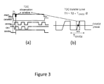
- an offset delay (T1) may be provided in the TDC 15 to compensate for the offset delay (T2) introduced by the first subset of components in the feedback loop arranged for generating the enable signal, e.g. the snapshot circuit, as shown in figure 2 . Therefore, the reference and enable signal are provided with a first (T1),and second (T2) offset delay. In this way, the reference and enable signal are sampled by the TDC 15 within the TDC observation window as shown in figure 3a .
- the first offset delay, e.g. TDC offset delay (T1) may be chosen to be around half the DCO output signal period, e.g.
- the TDC offset delay (T1) and the snapshot offset delay (T2) may be different from the desired values.
- the TDC 15 may operate outside of the predetermined observation window.
- Figure 4a shows the case when the TDC offset delay is too short.
- the TDC offset delay T1 is not sufficient to compensate the delay introduced by the snapshot circuit T2.
- the snapshot circuit 14 will have more chances to miss the expected CKVD2 edge and capture the next CKVD2 edge. Therefore, the probability of the TDC output code having more ones than zeros will be higher than expected as shown in figure 4b .
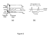
- T1 may be longer than the snapshot circuit delay (T2) resulting in the snapshot circuit 14 to capture the previous CKVD2 edge instead of the expected edge.
- T2 the TDC output code will have a higher probability to generate more zeros than ones, as shown in figure 5b .
- the TDC circuit 15 may be provided with an offset calibration system, as shown in figure 6 .
- the offset calibration system may be connected to the TDC output, which when activated may be arranged for evaluating the difference between the first and second offset delay values by monitoring the TDC output code generated over a predetermined period of time. Based on the TDC output code the calibration system may be arranged for adjusting the difference between the first (T1) and second (T2) offset delay values so as to position the predetermined observation window with respect to the reference signal.
- any variations in the first (T1) and second (T2) offset delay values may be compensated, thereby ensuring that the reference and enable signals are sampled by the TDC within the predetermined observation window. It has been found that by providing a calibration system which when activated is arranged for evaluating the difference between the first and second offset delay values, the difference between the first and second offset delay values may be dynamically adjusted so that the TDC is activated within the predetermined observation window. By processing the TDC output code, which is indicative of the phase difference between the reference signal and the enable signal, it is possible to determine whether the reference signal arrived within the predetermined time difference from the enable signal. As a result based on the TDC output code generated over a predetermined period of time the delay difference between the first and second offset delay values may be adjusted to position the TDC observation window with respect to the reference signal.
- the calibration system may comprise an offset calibration unit 152, as shown in figure 6 , connected to the TDC output and arranged for evaluating the difference between the first (T1) and second (T2) offset delays values and accordingly generate a delay adjustment control signal.
- the calibration system may further comprise a variable delay unit 153 connected to the offset calibration unit 152 and arranged for adjusting the first offset delay on the basis of the delay adjustment control signal.
- the variable delay unit may be part of the TDC 15.
- the first offset delay may be dynamically adjusted such that the TDC observation window is placed at the centre of the TDC transfer curve.
- the calibration system may be arranged for adjusting the difference between the first (T1) and second (T2) offset delay values in such a way that a transition edge of said reference signal is positioned substantially in the middle of said predetermined observation window, e.g by positioning the transition edge of the reference signal in the middle of the TDC transfer function.
- the delay adjustment control signal may be indicative of an offset delay adjustment value to be effected by the variable delay unit.
- the variable delay unit 153 may be a digitally-controlled programmable variable delay arranged for adjusting the delay of the reference signal, FREF dly, , based on the delay adjustment control signal generated by the calibration unit 152, which may be indicative of the value by which the first offset delay (T1) needs to be adjusted so that the reference signal arrives within the predetermined observation window.
- any variations introduced in the first and second offset delay values may be compensated, thereby ensuring that the TDC operates in the predetermined observation window.
- any variations in the first (T1) and second offset (T2) delay values may be dynamically adjusted, thereby ensuring the correct functionality of the TDC, which may lead to a higher performing ADPLL.
- the calibration unit may be further arranged for adjusting the second offset T2 in a similar manner to that described above with regards to the adjustments effected to the first offset.
- the calibration unit may be arranged for adjusting based on the TDC output the second offset T2 by means of a variable delay unit.
- the calibration unit may be arranged for adjusting on the basis of the TDC output both the first and second offset delays T1 and T2 by means of at least one variable delay unit.
- the calibration unit 152 may be arranged for evaluating the difference between the first and second offset delay values by accumulating the number of ones and zeros in the TDC output code generated over a predetermined period of time.
- this may be achieved by providing at least one counter 157, which is arranged for counting the number of ones and zeros in the TDC output code.
- the counter 157 may be connected to the Most Significant Bit (MSB) of the TDC output code, and arranged for counting the number of ones and zeros generated by the MSB over a predetermined period of time.
- MSB Most Significant Bit
- a calibration unit 152 may be provided with a TDC offset control unit 156 arranged for generating the delay adjustment control signal, which is used for controlling the variable delay unit 153.
- the TDC offset control unit 156 may be arranged for generating based on the value of the counter, a delay adjustment control signal for adjusting the first offset delay value (T1).
- T1 first offset delay value
- the TDC offset control unit 156 may be arranged for increasing the offset delay of the reference signal when the number of zeros is greater than the number of ones in the TDC output code.
- the TDC offset control unit 156 may be arranged for decreasing the offset delay of the reference signal when the number of ones is greater than the number of zeros.
- the TDC 15 may be a flash TDC arranged for generating a TDC output code indicative of the phase difference between the reference signal and the enable signal measured within the predetermined observation window.
- TDC 15 may be provided with a number of delay stages 154, each arranged for comparing the reference signal to the enable signal.
- the calibration system may be activated off-line, i.e. when the ADPLL is not in operation, so as to calibrate the first (T1) and second (T2) offset delays before operating the ADPLL.
- the calibration system may be activated on-line, i.e. before every phase dictation by the TDC. In this way, any variations introduced in the first and second offset delay values due to noise or temperature during the operation of the ADPLL may be compensated.
- FIG. 7 shows an example of measuring the TDC transfer function during ADPLL phase locking.
- Phase locking in PLLs has two phases. First is frequency acquisition which bring the variable clock frequency close to the targeted frequency. Once the variable clock (CKVD2) is close enough to the targeted frequency, the PLL may move to the second phase, phase tracking, to align the phases between variable and reference clocks. If the TDC, which acts as a phase difference digitizer, gives an output approaching zero, then it means the phases of the two clocks are aligned.
- the phase difference between the reference phase e.g., FREF dly
- variable clock e.g., CKVD2
- continuously rotates and the TDC gives an output which continuously sweeps all of the codes, as shown in Fig.
Landscapes
- Physics & Mathematics (AREA)
- General Physics & Mathematics (AREA)
- Stabilization Of Oscillater, Synchronisation, Frequency Synthesizers (AREA)
- Manipulation Of Pulses (AREA)
Abstract
Description
- The present disclosure relates to an All-Digital-Phase-Locked-Loop (ADPLL) and more specifically to an ADPLL having a TDC with a dynamically adjustable offset delay.
- Ultra-low-power (ULP) transceivers enable short-range networks of autonomous sensor nodes for wireless personal area network (WPAN) applications, e.g., Bluetooth Smart and Zigbee. RF Phase-Locked-Loops (PLL) for frequency synthesis and modulation consume a significant share of the total transceiver power, making sub-mW PLLs key to realize ULP WPAN radios. Compared to analog PLLs, all-digital PLLs (ADPLLs) are preferred in nanoscale CMOS as they offer benefit from smaller area overhead, programmability, capability of extensive self-calibrations, and easy portability. However, analog PLLs currently still dominate the field of ULP WPAN radios, since the time-to-digital-converter (TDC) of an ADPLL has traditionally been power hungry.
- A known approach for minimising the power consumption of a TDC circuit in the ADPLL is to reduce the activity of the TDC so that it operates only within a predetermined observation window. Such a TDC is known from J. Zhuang, et al., "A Low-Power All-Digital PLL Architecture Based on Phase Prediction," ICECS, 2012, where a 2.1-2.7GHz fractional-N ADPLL for WPAN applications DTC-assisted snapshot TDC is presented. In this implementation TDC snapshotting is implemented to reduce the sampling rate of the TDC from FCKVD2 to FREF. A Digital-to-Time Converter (DTC) is provided for reducing the detection range of the TDC detection range to less than 1/10 of the DCO output signal period, leading to a significant power reduction. The accumulated fractional part of the frequency command word, FCWfrac, controls the DTC to delay the reference signal FREF such that the delayed reference clock FREFdly is almost aligned with CKVD2, once the loop is locked. FREFdly also triggers the snapshot to catch the first CKVD2 edge so that only one CKVD2 edge, CKVD2S, per reference period is fed to the TDC. By capturing only one edge, the snapshot technique guarantees that the TDC has the minimum activity and consume minimum power. Moreover, the snapshotting also minimize the supply switch noise during TDC operation. A reduced-range TDC operating at the reference frequency (32MHz) then compares the edge of CKVD2S with FREFdly to provide the fractional phase error, PHEF. This approach reduces both sampling speed and detection range of TDC, leading to around 200x power reduction. In the snapshot TDC, the narrow observation window is opened by the CKVD2s, which acts as a TDC enable signal, after the rising edge of FREFdly. Since the TDC captures only the first rising edge of the variable clock, CDVD2, after the rising edge of FREFdly, the timing of opening TDC observation window is critical. In order to compensate for the delay added by the snapshot circuit, a TDC "offset delay" (T1) is added between the rising edge of FREFdly and the TDC observation window. However, the TDC and snapshot circuit offset delays cannot be easily estimated due to parasitic or slow logic transitions introduced in the layout during the design phase or during operation. As a result, due to the mismatch between the TDC and snapshot offset delays the TDC may be activated outside of the predetermined observation window, thereby causing the TDC to generate an erroneous output code, resulting in the degradation of the overall PLL performance, e.g. by introducing unwanted phase noise, and sometimes may even lead to an unstable PLL locking.
- It is an aim of the present disclosure to provide an ADPLL system which does not show the drawbacks of the prior art.
- This aim is achieved according to the disclosure with the ADPLL system showing the technical characteristics of the first independent claim.
- More in particular, according to embodiments of the present disclosure an All-Digital-Phase-Locked-Loop (ADPLL) comprising a Digitally Controlled Oscillator, DCO, arranged for generating a DCO output signal, and a feedback loop comprising a set of components for controlling the DCO. The components provided in the feedback loop comprises a Time-to-Digital Converter, TDC, provided for performing phase detection within a predetermined observation window, the TDC being arranged for receiving at least a reference signal having a first offset delay and an enable signal having a second offset delay and defining the predetermined observation window. The TDC is arranged for generating a TDC output code indicative of the phase difference between the reference signal and the enable signal measured within the predetermined observation window. A subset of the components in the feedback loop are arranged for generating the enable signal from the DCO output signal, such that the enable signal contains a transition edge derived from the DCO output signal and is arranged for activating the TDC so as to measure the phase difference between the reference signal and the enable signal within the predetermined observation window. The set of components of the feedback loop comprises an offset calibration system, connected to the TDC output, which when activated is arranged for evaluating the difference between the first and second offset delay values by monitoring the TDC output code generated over a predetermined period of time and for adjusting said difference to position the predetermined observation window with respect to the reference signal.
- It has been found that by providing a calibration system which when activated is arranged for evaluating the difference between the first and second offset delay values, the difference between the first and second offset delay values may be dynamically adjusted so that the TDC is activated within the predetermined observation window. By processing the TDC output code, which is indicative of the phase difference between the reference and the enable signal, it is possible to determine whether the reference signal arrived within the predetermined time difference from the enable signal. As a result based on the TDC output code generated over a predetermined period of time the delay difference between the first and second offset delay values may be adjusted to position the TDC observation window with respect to the reference signal, thereby ensuring that the TDC is operated within the predetermined observation window leading to a higher performing ADPLL.
- According to embodiments of the present disclosure, the calibration system is provided with an offset calibration unit, which is connected to the TDC output. The calibration unit is arranged for performing the evaluation of the difference between the first and second offset delay values and accordingly generating a delay adjustment control signal. The calibration system may further be provided with a variable delay unit, which is connected to the offset calibration unit and arranged for adjusting the first offset delay on the basis of the delay adjustment control signal.
- It has been found that by providing a calibration unit arranged for generating based on the TDC output code a delay adjustment control signal, which is used for controlling a variable delay unit, the first offset delay may be dynamically adjusted so that the reference signal arrives within the TDC observation window. In this way, offset delay adjustments may be effected without any external intervention purely based on the TDC output code. The delay adjustment control signal may be indicative of an offset delay adjustment value to be effected by the variable delay unit. The variable delay unit may be a digitally-controlled programmable variable delay arranged for adjusting the delay of the reference signal based on the delay adjustment control signal generated by the calibration unit, which may be indicative of the value by which the first offset delay needs to be adjusted so that the reference signal arrives within the predetermined observation window. In this way, any variations introduced in the first and second offset delay values may be compensated, thereby ensuring that the TDC operates in the predetermined observation window. As a result, with the system of the present disclosure any variations in the first and second offset delays may be dynamically compensated, thereby ensuring the correct functionality of the TDC, leading to a higher performing ADPLL.
- According to embodiments of the present disclosure, the difference between the first and second offset delay values is adjusted in such a way that a transition edge of said reference signal is positioned substantially in the middle of said predetermined observation window.. By positioning the reference signal in the middle of the predetermined observation window it is ensured that the TDC is provided with sufficient margin to both previous and the proceeding DCO output signal cycles.
- According to embodiments of the present disclosure, the calibration unit is arranged for evaluating the difference between the first and second offset delay values by accumulating the number of ones and zeros generated by the TDC output code over the predetermined period of time. For example, the calibration unit may be provided with at least one counter for counting the number of ones and zeros generated by the TDC output code over the predetermined period of time. For example, the counter may be arranged for the counting the number of ones and zeros generated by the Most Significant Bit (MSB) of the TDC output code. It has been found that by accumulating the number of ones and zeros in the TDC output code generated over a predetermined period of time provides a simple and effective way of determining whether the TDC is operated within the predetermined observation window. This is because the number of ones and zeros in the TDC output code generated over a predetermined period of time is directly related to the phase difference between the reference signal and the enable signal and vice versa. As a result, by observing the distribution of the ones and zeros in the TDC output code over the predetermined period of time the phase difference between the reference and enable signal may be easily evaluated.
- According to embodiments of the present disclosure, the ADPLL may comprise a TDC offset control unit arranged for generating the delay adjustment control signal based on the accumulated number of ones and zeros in the TDC output code. In this way, the first offset delay of the reference signal may be dynamically adjusted without any external intervention. For example, the TDC offset control unit may be arranged for increasing the offset delay of the reference signal when the number of zeros is greater than the number of ones in the TDC output code. The TDC offset control unit may also be arranged for decreasing the offset delay of the reference signal when the number of ones is greater than the number of zeros.
- The disclosure will be further elucidated by means of the following description and the appended figures.
-
Figure 1 shows a prior art ADPLL circuit. -
Figure 2 shows a representation of the offset delays in an ADPLL TDC circuit. -
Figure 3(a) and 3(b) shows a representation of TDC transfer curve when the TDC operates within the predetermined observation window. -
Figures 4(a) to 4(b) and5(a) to 5(b) show representations of the TDC transfer curve when it operates outside of the predetermined observation window. -
Figure 6 shows a representation of a TDC according to embodiments of the present disclosure. -
Figure 7 shows an example of an ADPLL phase locking procedure. - The present disclosure will be described with respect to particular embodiments and with reference to certain drawings but the disclosure is not limited thereto but only by the claims. The drawings described are only schematic and are non-limiting. In the drawings, the size of some of the elements may be exaggerated and not drawn on scale for illustrative purposes. The dimensions and the relative dimensions do not necessarily correspond to actual reductions to practice of the disclosure.
- Furthermore, the terms first, second, third and the like in the description and in the claims, are used for distinguishing between similar elements and not necessarily for describing a sequential or chronological order. The terms are interchangeable under appropriate circumstances and the embodiments of the disclosure can operate in other sequences than described or illustrated herein.
- Moreover, the terms top, bottom, over, under and the like in the description and the claims are used for descriptive purposes and not necessarily for describing relative positions. The terms so used are interchangeable under appropriate circumstances and the embodiments of the disclosure described herein can operate in other orientations than described or illustrated herein.
- Furthermore, the various embodiments, although referred to as "preferred" are to be construed as exemplary manners in which the disclosure may be implemented rather than as limiting the scope of the disclosure.
- The term "comprising", used in the claims, should not be interpreted as being restricted to the elements or steps listed thereafter; it does not exclude other elements or steps. It needs to be interpreted as specifying the presence of the stated features, integers, steps or components as referred to, but does not preclude the presence or addition of one or more other features, integers, steps or components, or groups thereof. Thus, the scope of the expression "a device comprising A and B" should not be limited to devices consisting only of components A and B, rather with respect to the present disclosure, the only enumerated components of the device are A and B, and further the claim should be interpreted as including equivalents of those components.
- Embodiments of the present disclosure will be explained with reference to the examples shown in
figures 1 to 7 . -
Figure 1 shows an example of anADPLL circuit 10, which is arranged for generating using a Digital Control Oscillator (DCO) 11 a DCO output signal, e.g. CKV, having a predetermined frequency. The ADPLL is arranged for receiving a reference frequency signal, e.g. FREF, and generate based on a Frequency Code Word (FCW), which may be multiple of the reference signal, the desired DCO output signal, e.g. CKV. In order to ensure that the DCO is maintained stable within the desired frequency range, the ADPLL may be provided with a feedback loop comprising a set of components for controlling the DCO. The components in the feedback loop comprise components for phase detection, which may be done in stages by means of for example a subset for detecting a coarse part of the phase e.g. using a phase incrementor for detecting the integer part of the phase, and a subset for detecting a fine part of the phase, for example a subset for detecting the fractional part of the phase. One of such components for detecting a fine part or a fractional part of the phase may be a Time-to-Digital Converter (TDC) 15 arranged for performing phase detection within a predetermined observation window. TheTDC 15 may be arranged for receiving at least a reference signal having a first offset delay and an enable signal having a second offset delay and defining the predetermined observation window. TheTDC 15 may be arranged for generating a TDC output code indicative of the phase difference between the reference signal and the enable signal measured within the predetermined observation window. For example, theTDC 15 may be arranged for measuring the fractional phase differences between the significant edge of the enable signal and the reference signal and accordingly generate a TDC output indicative of the fractional phase error (PHEf). TheTDC 15 may be arranged for performing phase detection between a reference signal and an enable signal derived from the DCO output signal, e.g. CKV, within a predetermined observation window. To generate the enable signal, the feedback loop may be provided with a first subset of components arranged for generating the enable signal based on a reduced rate DCO output signal, e.g. CKVD2, generated from amultiphase divider 13 such that the enable signal contains a transition edge derived from the DCO output signal. The enable signal generated may be arranged for activating theTDC 15 so as to measure the phase difference between the reference signal and the enable signal within the predetermined observation window. For example, the first subset of components may comprise asnapshotting circuit 14, which may be triggered by the reference signal for generating an enable signal representing at least one edge of the reduced rate DCO signal, e.g. CKVD2. In this way, only one edge of the reduced rate DCO signal, e.g. may be fed to the TDC per reference period, thereby reducing the activity of theTDC 15 leading to a reduced power consumption. By using the reference signal, e.g. FREF, for generating the enable signal which in turns activates theTDC 15, the sampling rate of theTDC 15 may be reduced to the frequency rate of the reference signal. In order to reduce the dynamic range of theTDC 15, a second subset of components may be provided, which may be arranged for positioning the reference signal within the predetermined observation window of the TDC. For example, this may be achieved by providing a Digital-to-Time Converter (DTC) 16, which may be arranged for delaying the reference signal, e.g., FREFdly, based on a phase setting control signal generated on the basis of FCW. In this way, a reducedrange TDC 15 may be provided for performing the fractional phase detection, thereby reducing the area overhead of theADPLL 10. - In order to ensure that the reference signal, e.g., FREFdly, arrives within the predetermined observation window, an offset delay (T1) may be provided in the
TDC 15 to compensate for the offset delay (T2) introduced by the first subset of components in the feedback loop arranged for generating the enable signal, e.g. the snapshot circuit, as shown infigure 2 . Therefore, the reference and enable signal are provided with a first (T1),and second (T2) offset delay. In this way, the reference and enable signal are sampled by theTDC 15 within the TDC observation window as shown infigure 3a . The first offset delay, e.g. TDC offset delay (T1) may be chosen to be around half the DCO output signal period, e.g. half the CLVD2 period, more than the second offset delay e.g. snapshot delay T2, such that the TDC observation window is placed at the centre of the TDC transfer curve so as to be provided with sufficient margin to both previous and the proceeding DCO output signal cycles, as show infigure 3b . - However, due to process variation, noise or other parasitic introduced in the layout of the ADPLL or during operation, the TDC offset delay (T1) and the snapshot offset delay (T2) may be different from the desired values. As a result the
TDC 15 may operate outside of the predetermined observation window.Figure 4a shows the case when the TDC offset delay is too short. In this case, the TDC offset delay T1 is not sufficient to compensate the delay introduced by the snapshot circuit T2. As a result, thesnapshot circuit 14 will have more chances to miss the expected CKVD2 edge and capture the next CKVD2 edge. Therefore, the probability of the TDC output code having more ones than zeros will be higher than expected as shown infigure 4b . This behaviour may be considered to be equivalent to the TDC observation window being placed close to the previous detection CKVD2 cycle. Similarly infigure 5a , the TDC offset delay (T1) may be longer than the snapshot circuit delay (T2) resulting in thesnapshot circuit 14 to capture the previous CKVD2 edge instead of the expected edge. As a result, the TDC output code will have a higher probability to generate more zeros than ones, as shown infigure 5b . - According to embodiments of the present disclosure, in order to compensate for variations in the first and second offset delays, the
TDC circuit 15 may be provided with an offset calibration system, as shown infigure 6 . The offset calibration system, may be connected to the TDC output, which when activated may be arranged for evaluating the difference between the first and second offset delay values by monitoring the TDC output code generated over a predetermined period of time. Based on the TDC output code the calibration system may be arranged for adjusting the difference between the first (T1) and second (T2) offset delay values so as to position the predetermined observation window with respect to the reference signal. As a result, any variations in the first (T1) and second (T2) offset delay values may be compensated, thereby ensuring that the reference and enable signals are sampled by the TDC within the predetermined observation window. It has been found that by providing a calibration system which when activated is arranged for evaluating the difference between the first and second offset delay values, the difference between the first and second offset delay values may be dynamically adjusted so that the TDC is activated within the predetermined observation window. By processing the TDC output code, which is indicative of the phase difference between the reference signal and the enable signal, it is possible to determine whether the reference signal arrived within the predetermined time difference from the enable signal. As a result based on the TDC output code generated over a predetermined period of time the delay difference between the first and second offset delay values may be adjusted to position the TDC observation window with respect to the reference signal. - According to embodiments of the present disclosure, the calibration system may comprise an offset
calibration unit 152, as shown infigure 6 , connected to the TDC output and arranged for evaluating the difference between the first (T1) and second (T2) offset delays values and accordingly generate a delay adjustment control signal. The calibration system may further comprise avariable delay unit 153 connected to the offsetcalibration unit 152 and arranged for adjusting the first offset delay on the basis of the delay adjustment control signal. The variable delay unit may be part of theTDC 15. It has been found that by providing acalibration unit 152 arranged for generating based on the TDC output code a delay adjustment control signal, which is used for controlling avariable delay unit 153, the first offset delay may be dynamically adjusted such that the TDC observation window is placed at the centre of the TDC transfer curve. For example, the calibration system may be arranged for adjusting the difference between the first (T1) and second (T2) offset delay values in such a way that a transition edge of said reference signal is positioned substantially in the middle of said predetermined observation window, e.g by positioning the transition edge of the reference signal in the middle of the TDC transfer function. By providing a calibration system, the offset delay adjustments may be effected without any external intervention purely based on the TDC output code. The delay adjustment control signal may be indicative of an offset delay adjustment value to be effected by the variable delay unit. For example, thevariable delay unit 153 may be a digitally-controlled programmable variable delay arranged for adjusting the delay of the reference signal, FREFdly,, based on the delay adjustment control signal generated by thecalibration unit 152, which may be indicative of the value by which the first offset delay (T1) needs to be adjusted so that the reference signal arrives within the predetermined observation window. In this way, any variations introduced in the first and second offset delay values may be compensated, thereby ensuring that the TDC operates in the predetermined observation window. As a result, with the system of the present disclosure any variations in the first (T1) and second offset (T2) delay values may be dynamically adjusted, thereby ensuring the correct functionality of the TDC, which may lead to a higher performing ADPLL. - According to embodiments of the present disclosure, the calibration unit may be further arranged for adjusting the second offset T2 in a similar manner to that described above with regards to the adjustments effected to the first offset. For example, the calibration unit may be arranged for adjusting based on the TDC output the second offset T2 by means of a variable delay unit. Furthermore, the calibration unit may be arranged for adjusting on the basis of the TDC output both the first and second offset delays T1 and T2 by means of at least one variable delay unit.According to embodiments of the present disclosure, the
calibration unit 152 may be arranged for evaluating the difference between the first and second offset delay values by accumulating the number of ones and zeros in the TDC output code generated over a predetermined period of time. For example, this may be achieved by providing at least onecounter 157, which is arranged for counting the number of ones and zeros in the TDC output code. For example, thecounter 157 may be connected to the Most Significant Bit (MSB) of the TDC output code, and arranged for counting the number of ones and zeros generated by the MSB over a predetermined period of time. - According to embodiments of the present disclosure, a
calibration unit 152 may be provided with a TDC offsetcontrol unit 156 arranged for generating the delay adjustment control signal, which is used for controlling thevariable delay unit 153. The TDC offsetcontrol unit 156 may be arranged for generating based on the value of the counter, a delay adjustment control signal for adjusting the first offset delay value (T1). For example, the TDC offsetcontrol unit 156 may be arranged for increasing the offset delay of the reference signal when the number of zeros is greater than the number of ones in the TDC output code. Alternative, the TDC offsetcontrol unit 156 may be arranged for decreasing the offset delay of the reference signal when the number of ones is greater than the number of zeros. - According to embodiments of the present disclosure, the
TDC 15 may be a flash TDC arranged for generating a TDC output code indicative of the phase difference between the reference signal and the enable signal measured within the predetermined observation window. However, other TDC architecture know in the art may be employed. TheTDC 15, as shown infigure 6 , may be provided with a number of delay stages 154, each arranged for comparing the reference signal to the enable signal. - According to embodiments of the present disclosure, the calibration system may be activated off-line, i.e. when the ADPLL is not in operation, so as to calibrate the first (T1) and second (T2) offset delays before operating the ADPLL. According to alternative embodiments, the calibration system may be activated on-line, i.e. before every phase dictation by the TDC. In this way, any variations introduced in the first and second offset delay values due to noise or temperature during the operation of the ADPLL may be compensated.
-
Figure 7 shows an example of measuring the TDC transfer function during ADPLL phase locking. Phase locking in PLLs has two phases. First is frequency acquisition which bring the variable clock frequency close to the targeted frequency. Once the variable clock (CKVD2) is close enough to the targeted frequency, the PLL may move to the second phase, phase tracking, to align the phases between variable and reference clocks. If the TDC, which acts as a phase difference digitizer, gives an output approaching zero, then it means the phases of the two clocks are aligned. During the frequency acquisition phase, the phase difference between the reference phase, e.g., FREFdly, and variable clock, e.g., CKVD2, continuously rotates, and the TDC gives an output which continuously sweeps all of the codes, as shown inFig. 7 . This behaviour may be explained by the fact that the phase difference between the reference phase and variable phase is continuously rotating because of the frequency difference between the variable clock and targeted output. Hence, by reading out the TDC output during the frequency acquisition phase, the TDC transfer curve can be directly measured.
Claims (15)
- An All-Digital-Phase-Locked-Loop (10), ADPLL, comprising a Digitally Controlled Oscillator (11), DCO, arranged for generating a DCO output signal from a Frequency Code Word, FCW, and a feedback loop comprising a set of components for controlling the DCO (11), the components comprising:a Time-to-Digital Converter (15), TDC, provided for performing phase detection within a predetermined observation window, the TDC (15) being arranged for receiving at least a reference signal having a first offset delay and an enable signal having a second offset delay and defining the predetermined observation window, the TDC (15) being arranged for generating a TDC output code indicative of the phase difference between the reference signal and the enable signal measured within the predetermined observation window; anda subset of components arranged for generating the enable signal from the DCO output signal, such that the enable signal contains a transition edge derived from the DCO output signal and is arranged for activating the TDC (15) so as to measure the phase difference between the reference signal and the enable signal within the predetermined observation window;characterised in that the set of components of the feedback loop comprises an offset calibration system, connected to the TDC output, which when activated is arranged for evaluating the difference between the first and second offset delay values by monitoring the TDC output code generated over a predetermined period of time and for adjusting said difference to position the predetermined observation window with respect to the reference signal.
- The ADPLL (10) of claim 1, wherein the offset calibration system comprises an offset calibration unit (152), connected to the TDC output and arranged for performing said evaluation and accordingly generating a delay adjustment control signal, and a variable delay unit (153) connected to the offset calibration unit (152) and arranged for adjusting the first offset delay on the basis of the delay adjustment control signal.
- The ADPLL (10) of claim 2, wherein the variable delay unit (153) is part of the TDC (15).
- The ADPLL (10) of any one of the claims 1-3, wherein the offset calibration system is arranged for adjusting said difference in such a way that a transition edge of said reference signal is positioned substantially in the middle of said predetermined observation window.
- The ADPLL (10) of any one of the claims 1-3, wherein the offset calibration system is arranged for adjusting said difference in such a way that a transition edge of said reference signal is positioned substantially in the middle of the TDC transfer curve.
- The ADPLL (10) of any one of the preceding claims, wherein the calibration system is arranged for evaluating the difference between the first and second offset delay values by counting the number of ones and zeros generated by the Most Significant Bit of the TDC output code.
- The ADPLL of claim 6, wherein the offset calibration system comprises a TDC offset control unit (156) arranged for increasing the first offset delay when the number of zeros is greater than the number of ones in the TDC output code.
- The ADPLL (10) of claim 6 or 7, wherein the TDC offset control unit (156) is arranged for decreasing the first offset delay when the number of ones is greater than the number of zeros.
- The ADPLL (10) of any one of the preceding claims, wherein the feedback loop comprises components arranged for detecting a coarse part of the phase and components, among which the TDC (15), for detecting a fine part of the phase.
- The ADPLL (10) of any one of the preceding claims, wherein the feedback loop comprises components arranged for detecting an integer part of the phase and components, among which the TDC (15), for detecting a fractional part of the phase.
- The ADPLL (10) of any one of the preceding claims, wherein the TDC (15) is a flash TDC.
- A method for operating an All-Digital-Phase-Locked-Loop (10), ADPLL, comprising a Digitally Controlled Oscillator (11), DCO, arranged for generating a DCO output signal, and a feedback loop comprising a set of components for controlling the DCO (11), the method comprising the steps of:a) activating a Time-to-Digital Converter (15), TDC, arranged for performing phase detection within a predetermined observation window, the TDC (15) being arranged for receiving at least a reference signal having a first offset delay and an enable signal having a second offset delay and defining the predetermined observation window, wherein the step of activating the TDC (15) comprises the steps of :a1) providing a reference signal to the TDC (15), anda2) generating by means of a subset of components the enable signal from the DCO output signal, such that the enable signal contains a transition edge derived from the DCO output signal and is arranged for activating the TDC so as to measure the phase difference between the reference signal and the enable signal within the predetermined observation window;b) generating by means of the TDC (15) a TDC output code indicative of the phase difference between the reference signal and the enable signal measured within the predetermined observation window; andc) performing an offset delay calibration step by means of a calibration system connected to the TDC output, the calibration step comprising the steps of:c1) evaluating the difference between the first and second offset delay values by monitoring the TDC output code generated over a predetermined period of time, andc2) adjusting said difference to position the predetermined observation window with respect to the reference signal.
- The method of claim 12, wherein the offset delay calibration step comprises the steps of:generating a delay adjustment control signal based on the difference between the first and second offset delay values detected during the evaluation step, and applying the delay adjustment control signal to a variable delay unit to adjust the first offset delay.
- The method of claim 12 or 13, wherein the offset delay calibration step is performed off-line.
- The method of claim 12 or 13, wherein the offset calibration step performed is performed on-line during a frequency acquisition stage before activating the TDC for phase locking.
Priority Applications (3)
| Application Number | Priority Date | Filing Date | Title |
|---|---|---|---|
| EP14199426.9A EP3035536B1 (en) | 2014-12-19 | 2014-12-19 | An ADPLL having a TDC circuit with a dynamically adjustable offset delay |
| JP2015241291A JP6660165B2 (en) | 2014-12-19 | 2015-12-10 | ADPLL with TDC circuit having dynamically adjustable offset delay |
| US14/975,834 US9774336B2 (en) | 2014-12-19 | 2015-12-20 | All-digital-phase-locked-loop having a time-to-digital converter circuit with a dynamically adjustable offset delay |
Applications Claiming Priority (1)
| Application Number | Priority Date | Filing Date | Title |
|---|---|---|---|
| EP14199426.9A EP3035536B1 (en) | 2014-12-19 | 2014-12-19 | An ADPLL having a TDC circuit with a dynamically adjustable offset delay |
Publications (2)
| Publication Number | Publication Date |
|---|---|
| EP3035536A1 true EP3035536A1 (en) | 2016-06-22 |
| EP3035536B1 EP3035536B1 (en) | 2020-04-29 |
Family
ID=52278410
Family Applications (1)
| Application Number | Title | Priority Date | Filing Date |
|---|---|---|---|
| EP14199426.9A Active EP3035536B1 (en) | 2014-12-19 | 2014-12-19 | An ADPLL having a TDC circuit with a dynamically adjustable offset delay |
Country Status (3)
| Country | Link |
|---|---|
| US (1) | US9774336B2 (en) |
| EP (1) | EP3035536B1 (en) |
| JP (1) | JP6660165B2 (en) |
Cited By (9)
| Publication number | Priority date | Publication date | Assignee | Title |
|---|---|---|---|---|
| EP3306819A1 (en) * | 2016-10-06 | 2018-04-11 | Analog Devices, Inc. | Phase control of clock signal based on feedback |
| EP3327461A1 (en) * | 2016-11-23 | 2018-05-30 | NXP USA, Inc. | Digital synthesizer, radar device and method therefor |
| CN111231398A (en) * | 2018-11-28 | 2020-06-05 | 中国科学院宁波材料技术与工程研究所 | Control method of double steel belt press |
| USRE48735E1 (en) * | 2017-12-11 | 2021-09-14 | Silicon Laboratories Inc. | Use of a recirculating delay line with a time-to-digital converter |
| CN114047682A (en) * | 2021-11-16 | 2022-02-15 | 华南理工大学 | Time-to-digital converter with PVT robustness based on fully differential ring oscillator |
| CN115038162A (en) * | 2022-08-12 | 2022-09-09 | 广州安凯微电子股份有限公司 | Method and device for rapid same-frequency and same-phase adjustment of Bluetooth clock |
| CN116015285A (en) * | 2022-12-31 | 2023-04-25 | 成都电科星拓科技有限公司 | A method and device for correcting TDC delay step based on stepping LDO |
| US20230185248A1 (en) * | 2020-04-24 | 2023-06-15 | Telefonaktiebolaget Lm Ericsson (Publ) | Time to digital converter arrangement with increased detection range |
| CN117394861A (en) * | 2023-12-12 | 2024-01-12 | 厦门电科星拓科技有限公司 | TDC unit compatible with spread spectrum and construction method |
Families Citing this family (18)
| Publication number | Priority date | Publication date | Assignee | Title |
|---|---|---|---|---|
| US9722537B2 (en) * | 2014-08-20 | 2017-08-01 | Short Circuit Technologies Llc | Fractional-N frequency synthesizer incorporating cyclic digital-to-time and time-to-digital circuit pair |
| JP6584885B2 (en) * | 2015-09-14 | 2019-10-02 | 株式会社東芝 | Equipment with noise removal function |
| CN108023723B (en) | 2016-11-04 | 2021-07-09 | 华为技术有限公司 | Method of frequency synchronization and slave clock |
| CN106898374B (en) * | 2017-01-10 | 2020-06-30 | 西安紫光国芯半导体有限公司 | Feedback circuit system with VDD self-compensation DLL for DRAM |
| US9948311B1 (en) * | 2017-01-31 | 2018-04-17 | Finisar Corporation | Decision-directed phase detector |
| US9954542B1 (en) | 2017-02-01 | 2018-04-24 | Apple Inc. | Digital linearization technique for charge pump based fractional phased-locked loop |
| US9979405B1 (en) * | 2017-02-10 | 2018-05-22 | Apple Inc. | Adaptively reconfigurable time-to-digital converter for digital phase-locked loops |
| US10320401B2 (en) * | 2017-10-13 | 2019-06-11 | Xilinx, Inc. | Dual-path digital-to-time converter |
| US10707879B2 (en) * | 2018-04-13 | 2020-07-07 | KaiKuTek Inc. | Frequency-modulated continuous-wave radar system and frequency tracking method for calibrating frequency gains of a radio frequency signal to approach wideband flatness frequency responses |
| US10642227B1 (en) * | 2019-03-15 | 2020-05-05 | Taiwan Semiconductor Manufacturing Co., Ltd. | Digital-to-time converter, time-to-digital converter, and converting method using the same |
| US11223362B2 (en) * | 2020-05-14 | 2022-01-11 | Mediatek Inc. | Phase-locked loop circuit and digital-to-time convertor error cancelation method thereof |
| CN111654281B (en) * | 2020-06-10 | 2023-08-04 | 上海兆芯集成电路股份有限公司 | time converter |
| CN114363132B (en) | 2020-10-13 | 2026-04-07 | 三星电子株式会社 | Communication method |
| US11942956B2 (en) | 2021-11-25 | 2024-03-26 | Samsung Electronics Co., Ltd. | Time-to-digital converter and digital phase-locked loop circuit comprising the same |
| CN116243583B (en) * | 2021-12-03 | 2025-04-29 | 中国科学院苏州纳米技术与纳米仿生研究所 | Neural network measurement calibration system and method for TDL-TDC |
| US12422519B2 (en) * | 2022-09-06 | 2025-09-23 | Infineon Technologies Ag | Real-time chirp signal frequency linearity measurement |
| US12249998B2 (en) * | 2022-09-06 | 2025-03-11 | Infineon Technologies Ag | Real-time chirp signal frequency linearity measurement |
| CN117914318B (en) * | 2024-01-31 | 2025-03-21 | 深圳市电科星拓科技有限公司 | Method and device for detecting snapshot circuit burrs in a fully digital phase-locked loop |
Citations (2)
| Publication number | Priority date | Publication date | Assignee | Title |
|---|---|---|---|---|
| US20090096535A1 (en) * | 2007-10-16 | 2009-04-16 | Hsiang-Hui Chang | All-Digital Phase-Locked Loop |
| US8570082B1 (en) * | 2013-02-27 | 2013-10-29 | Taiwan Semiconductor Manufacturing Co., Ltd. | PVT-free calibration circuit for TDC resolution in ADPLL |
Family Cites Families (3)
| Publication number | Priority date | Publication date | Assignee | Title |
|---|---|---|---|---|
| US20100260242A1 (en) * | 2008-03-04 | 2010-10-14 | Katsuaki Abe | Time digital converter, digital pll frequency synthesizer, transceiver, and receiver |
| JP2011525737A (en) * | 2008-06-20 | 2011-09-22 | ヴェリジー(シンガポール) プライベート リミテッド | Apparatus and method for evaluating data relating to time difference, and apparatus and method for calibrating a delay line |
| US8098085B2 (en) * | 2009-03-30 | 2012-01-17 | Qualcomm Incorporated | Time-to-digital converter (TDC) with improved resolution |
-
2014
- 2014-12-19 EP EP14199426.9A patent/EP3035536B1/en active Active
-
2015
- 2015-12-10 JP JP2015241291A patent/JP6660165B2/en active Active
- 2015-12-20 US US14/975,834 patent/US9774336B2/en active Active
Patent Citations (2)
| Publication number | Priority date | Publication date | Assignee | Title |
|---|---|---|---|---|
| US20090096535A1 (en) * | 2007-10-16 | 2009-04-16 | Hsiang-Hui Chang | All-Digital Phase-Locked Loop |
| US8570082B1 (en) * | 2013-02-27 | 2013-10-29 | Taiwan Semiconductor Manufacturing Co., Ltd. | PVT-free calibration circuit for TDC resolution in ADPLL |
Non-Patent Citations (2)
| Title |
|---|
| J. ZHUANG ET AL.: "A Low-Power All-Digital PLL Architecture Based on Phase Prediction", ICECS, 2012 |
| JINGCHENG ZHUANG ET AL: "A low-power all-digital PLL architecture based on phase prediction", ELECTRONICS, CIRCUITS AND SYSTEMS (ICECS), 2012 19TH IEEE INTERNATIONAL CONFERENCE ON, IEEE, 9 December 2012 (2012-12-09), pages 797 - 800, XP032331578, ISBN: 978-1-4673-1261-5, DOI: 10.1109/ICECS.2012.6463539 * |
Cited By (20)
| Publication number | Priority date | Publication date | Assignee | Title |
|---|---|---|---|---|
| CN107918444A (en) * | 2016-10-06 | 2018-04-17 | 美国亚德诺半导体公司 | Phase control based on feedback clock signal |
| US10305495B2 (en) | 2016-10-06 | 2019-05-28 | Analog Devices, Inc. | Phase control of clock signal based on feedback |
| EP3306819A1 (en) * | 2016-10-06 | 2018-04-11 | Analog Devices, Inc. | Phase control of clock signal based on feedback |
| US10727842B2 (en) | 2016-10-06 | 2020-07-28 | Analog Devices, Inc. | Bi-directional interface for device feedback |
| EP3327461A1 (en) * | 2016-11-23 | 2018-05-30 | NXP USA, Inc. | Digital synthesizer, radar device and method therefor |
| US10097187B2 (en) | 2016-11-23 | 2018-10-09 | Nxp Usa, Inc. | Digital synthesizer, radar device and method therefor |
| USRE48735E1 (en) * | 2017-12-11 | 2021-09-14 | Silicon Laboratories Inc. | Use of a recirculating delay line with a time-to-digital converter |
| CN111231398B (en) * | 2018-11-28 | 2022-11-04 | 中国科学院宁波材料技术与工程研究所 | Control method of double steel belt press |
| CN111231398A (en) * | 2018-11-28 | 2020-06-05 | 中国科学院宁波材料技术与工程研究所 | Control method of double steel belt press |
| US20230185248A1 (en) * | 2020-04-24 | 2023-06-15 | Telefonaktiebolaget Lm Ericsson (Publ) | Time to digital converter arrangement with increased detection range |
| US11774915B2 (en) * | 2020-04-24 | 2023-10-03 | Telefonaktiebolaget Lm Ericsson (Publ) | Time to digital converter arrangement with increased detection range |
| US20230418237A1 (en) * | 2020-04-24 | 2023-12-28 | Telefonaktiebolaget Lm Ericsson (Publ) | Time to digital converter arrangement with increased detection range |
| US12032341B2 (en) * | 2020-04-24 | 2024-07-09 | Telefonaktiebolaget Lm Ericsson (Publ) | Time to digital converter arrangement with increased detection range |
| CN114047682A (en) * | 2021-11-16 | 2022-02-15 | 华南理工大学 | Time-to-digital converter with PVT robustness based on fully differential ring oscillator |
| CN115038162A (en) * | 2022-08-12 | 2022-09-09 | 广州安凯微电子股份有限公司 | Method and device for rapid same-frequency and same-phase adjustment of Bluetooth clock |
| CN115038162B (en) * | 2022-08-12 | 2022-11-18 | 广州安凯微电子股份有限公司 | Method and device for rapid same-frequency and same-phase adjustment of Bluetooth clock |
| CN116015285A (en) * | 2022-12-31 | 2023-04-25 | 成都电科星拓科技有限公司 | A method and device for correcting TDC delay step based on stepping LDO |
| CN116015285B (en) * | 2022-12-31 | 2024-03-12 | 成都电科星拓科技有限公司 | A method and device for correcting TDC delay step based on stepping LDO |
| CN117394861A (en) * | 2023-12-12 | 2024-01-12 | 厦门电科星拓科技有限公司 | TDC unit compatible with spread spectrum and construction method |
| CN117394861B (en) * | 2023-12-12 | 2024-03-12 | 厦门电科星拓科技有限公司 | TDC unit compatible with spread spectrum and construction method |
Also Published As
| Publication number | Publication date |
|---|---|
| JP6660165B2 (en) | 2020-03-11 |
| US9774336B2 (en) | 2017-09-26 |
| EP3035536B1 (en) | 2020-04-29 |
| US20160182067A1 (en) | 2016-06-23 |
| JP2016119663A (en) | 2016-06-30 |
Similar Documents
| Publication | Publication Date | Title |
|---|---|---|
| EP3035536B1 (en) | An ADPLL having a TDC circuit with a dynamically adjustable offset delay | |
| US10707854B2 (en) | Clock screening with programmable counter-based clock interface and time-to-digital converter with high resolution and wide range operation | |
| US10644869B2 (en) | Automatic detection of change in PLL locking trend | |
| US8638146B1 (en) | Dual mode phase detection | |
| CN107896106B (en) | Frequency synthesis system, phase-locked loop and method for adjusting phase of digital phase-locked loop | |
| KR20100062893A (en) | Time-to-digital convertoer and all-digital phase locked loop | |
| US11888480B2 (en) | Method and apparatus for synchronizing two systems | |
| US10018970B2 (en) | Time-to-digital system and associated frequency synthesizer | |
| WO2012177491A1 (en) | Phase-locked loop lock detect | |
| JP6647981B2 (en) | All digital phase locked loop | |
| EP3035535A1 (en) | ADPLL with a TDC having a reduced DTC range | |
| US8686768B2 (en) | Phase locked loop | |
| CN105281752A (en) | Clock data recovery system based on digital phase-locked loop | |
| CN107911114A (en) | A kind of broadband phase-looked loop of constant loop bandwidth | |
| US9621171B1 (en) | Frequency scaling method, circuit and associated all-digital phase-locked loop | |
| US11387781B1 (en) | Fast start-up crystal oscillator and fast start-up method thereof | |
| CN105959001B (en) | Become frequency domain all-digital phase-locked loop and locking phase control method | |
| US9893878B1 (en) | On-chip jitter measurement for clock circuits | |
| Zhuang et al. | Gain estimation of a digital-to-time converter for phase-prediction all-digital PLL | |
| US7443251B2 (en) | Digital phase and frequency detector | |
| US8138801B1 (en) | Frequency crossing detection using opposing pattern detectors | |
| JP2012065252A (en) | Clock extraction circuit and receiver |
Legal Events
| Date | Code | Title | Description |
|---|---|---|---|
| PUAI | Public reference made under article 153(3) epc to a published international application that has entered the european phase |
Free format text: ORIGINAL CODE: 0009012 |
|
| AK | Designated contracting states |
Kind code of ref document: A1 Designated state(s): AL AT BE BG CH CY CZ DE DK EE ES FI FR GB GR HR HU IE IS IT LI LT LU LV MC MK MT NL NO PL PT RO RS SE SI SK SM TR |
|
| AX | Request for extension of the european patent |
Extension state: BA ME |
|
| STAA | Information on the status of an ep patent application or granted ep patent |
Free format text: STATUS: REQUEST FOR EXAMINATION WAS MADE |
|
| 17P | Request for examination filed |
Effective date: 20161108 |
|
| RBV | Designated contracting states (corrected) |
Designated state(s): AL AT BE BG CH CY CZ DE DK EE ES FI FR GB GR HR HU IE IS IT LI LT LU LV MC MK MT NL NO PL PT RO RS SE SI SK SM TR |
|
| GRAP | Despatch of communication of intention to grant a patent |
Free format text: ORIGINAL CODE: EPIDOSNIGR1 |
|
| STAA | Information on the status of an ep patent application or granted ep patent |
Free format text: STATUS: GRANT OF PATENT IS INTENDED |
|
| INTG | Intention to grant announced |
Effective date: 20191127 |
|
| GRAS | Grant fee paid |
Free format text: ORIGINAL CODE: EPIDOSNIGR3 |
|
| GRAA | (expected) grant |
Free format text: ORIGINAL CODE: 0009210 |
|
| STAA | Information on the status of an ep patent application or granted ep patent |
Free format text: STATUS: THE PATENT HAS BEEN GRANTED |
|
| AK | Designated contracting states |
Kind code of ref document: B1 Designated state(s): AL AT BE BG CH CY CZ DE DK EE ES FI FR GB GR HR HU IE IS IT LI LT LU LV MC MK MT NL NO PL PT RO RS SE SI SK SM TR |
|
| REG | Reference to a national code |
Ref country code: GB Ref legal event code: FG4D |
|
| REG | Reference to a national code |
Ref country code: CH Ref legal event code: EP |
|
| REG | Reference to a national code |
Ref country code: AT Ref legal event code: REF Ref document number: 1264848 Country of ref document: AT Kind code of ref document: T Effective date: 20200515 |
|
| REG | Reference to a national code |
Ref country code: DE Ref legal event code: R096 Ref document number: 602014064441 Country of ref document: DE |
|
| REG | Reference to a national code |
Ref country code: IE Ref legal event code: FG4D |
|
| REG | Reference to a national code |
Ref country code: NL Ref legal event code: MP Effective date: 20200429 |
|
| REG | Reference to a national code |
Ref country code: LT Ref legal event code: MG4D |
|
| PG25 | Lapsed in a contracting state [announced via postgrant information from national office to epo] |
Ref country code: IS Free format text: LAPSE BECAUSE OF FAILURE TO SUBMIT A TRANSLATION OF THE DESCRIPTION OR TO PAY THE FEE WITHIN THE PRESCRIBED TIME-LIMIT Effective date: 20200829 Ref country code: LT Free format text: LAPSE BECAUSE OF FAILURE TO SUBMIT A TRANSLATION OF THE DESCRIPTION OR TO PAY THE FEE WITHIN THE PRESCRIBED TIME-LIMIT Effective date: 20200429 Ref country code: GR Free format text: LAPSE BECAUSE OF FAILURE TO SUBMIT A TRANSLATION OF THE DESCRIPTION OR TO PAY THE FEE WITHIN THE PRESCRIBED TIME-LIMIT Effective date: 20200730 Ref country code: SE Free format text: LAPSE BECAUSE OF FAILURE TO SUBMIT A TRANSLATION OF THE DESCRIPTION OR TO PAY THE FEE WITHIN THE PRESCRIBED TIME-LIMIT Effective date: 20200429 Ref country code: NO Free format text: LAPSE BECAUSE OF FAILURE TO SUBMIT A TRANSLATION OF THE DESCRIPTION OR TO PAY THE FEE WITHIN THE PRESCRIBED TIME-LIMIT Effective date: 20200729 Ref country code: PT Free format text: LAPSE BECAUSE OF FAILURE TO SUBMIT A TRANSLATION OF THE DESCRIPTION OR TO PAY THE FEE WITHIN THE PRESCRIBED TIME-LIMIT Effective date: 20200831 Ref country code: FI Free format text: LAPSE BECAUSE OF FAILURE TO SUBMIT A TRANSLATION OF THE DESCRIPTION OR TO PAY THE FEE WITHIN THE PRESCRIBED TIME-LIMIT Effective date: 20200429 |
|
| REG | Reference to a national code |
Ref country code: AT Ref legal event code: MK05 Ref document number: 1264848 Country of ref document: AT Kind code of ref document: T Effective date: 20200429 |
|
| PG25 | Lapsed in a contracting state [announced via postgrant information from national office to epo] |
Ref country code: LV Free format text: LAPSE BECAUSE OF FAILURE TO SUBMIT A TRANSLATION OF THE DESCRIPTION OR TO PAY THE FEE WITHIN THE PRESCRIBED TIME-LIMIT Effective date: 20200429 Ref country code: RS Free format text: LAPSE BECAUSE OF FAILURE TO SUBMIT A TRANSLATION OF THE DESCRIPTION OR TO PAY THE FEE WITHIN THE PRESCRIBED TIME-LIMIT Effective date: 20200429 Ref country code: HR Free format text: LAPSE BECAUSE OF FAILURE TO SUBMIT A TRANSLATION OF THE DESCRIPTION OR TO PAY THE FEE WITHIN THE PRESCRIBED TIME-LIMIT Effective date: 20200429 Ref country code: BG Free format text: LAPSE BECAUSE OF FAILURE TO SUBMIT A TRANSLATION OF THE DESCRIPTION OR TO PAY THE FEE WITHIN THE PRESCRIBED TIME-LIMIT Effective date: 20200729 |
|
| PG25 | Lapsed in a contracting state [announced via postgrant information from national office to epo] |
Ref country code: NL Free format text: LAPSE BECAUSE OF FAILURE TO SUBMIT A TRANSLATION OF THE DESCRIPTION OR TO PAY THE FEE WITHIN THE PRESCRIBED TIME-LIMIT Effective date: 20200429 Ref country code: AL Free format text: LAPSE BECAUSE OF FAILURE TO SUBMIT A TRANSLATION OF THE DESCRIPTION OR TO PAY THE FEE WITHIN THE PRESCRIBED TIME-LIMIT Effective date: 20200429 |
|
| PG25 | Lapsed in a contracting state [announced via postgrant information from national office to epo] |
Ref country code: SM Free format text: LAPSE BECAUSE OF FAILURE TO SUBMIT A TRANSLATION OF THE DESCRIPTION OR TO PAY THE FEE WITHIN THE PRESCRIBED TIME-LIMIT Effective date: 20200429 Ref country code: EE Free format text: LAPSE BECAUSE OF FAILURE TO SUBMIT A TRANSLATION OF THE DESCRIPTION OR TO PAY THE FEE WITHIN THE PRESCRIBED TIME-LIMIT Effective date: 20200429 Ref country code: AT Free format text: LAPSE BECAUSE OF FAILURE TO SUBMIT A TRANSLATION OF THE DESCRIPTION OR TO PAY THE FEE WITHIN THE PRESCRIBED TIME-LIMIT Effective date: 20200429 Ref country code: DK Free format text: LAPSE BECAUSE OF FAILURE TO SUBMIT A TRANSLATION OF THE DESCRIPTION OR TO PAY THE FEE WITHIN THE PRESCRIBED TIME-LIMIT Effective date: 20200429 Ref country code: CZ Free format text: LAPSE BECAUSE OF FAILURE TO SUBMIT A TRANSLATION OF THE DESCRIPTION OR TO PAY THE FEE WITHIN THE PRESCRIBED TIME-LIMIT Effective date: 20200429 Ref country code: ES Free format text: LAPSE BECAUSE OF FAILURE TO SUBMIT A TRANSLATION OF THE DESCRIPTION OR TO PAY THE FEE WITHIN THE PRESCRIBED TIME-LIMIT Effective date: 20200429 Ref country code: IT Free format text: LAPSE BECAUSE OF FAILURE TO SUBMIT A TRANSLATION OF THE DESCRIPTION OR TO PAY THE FEE WITHIN THE PRESCRIBED TIME-LIMIT Effective date: 20200429 |
|
| REG | Reference to a national code |
Ref country code: DE Ref legal event code: R097 Ref document number: 602014064441 Country of ref document: DE |
|
| PG25 | Lapsed in a contracting state [announced via postgrant information from national office to epo] |
Ref country code: PL Free format text: LAPSE BECAUSE OF FAILURE TO SUBMIT A TRANSLATION OF THE DESCRIPTION OR TO PAY THE FEE WITHIN THE PRESCRIBED TIME-LIMIT Effective date: 20200429 Ref country code: SK Free format text: LAPSE BECAUSE OF FAILURE TO SUBMIT A TRANSLATION OF THE DESCRIPTION OR TO PAY THE FEE WITHIN THE PRESCRIBED TIME-LIMIT Effective date: 20200429 |
|
| PLBE | No opposition filed within time limit |
Free format text: ORIGINAL CODE: 0009261 |
|
| STAA | Information on the status of an ep patent application or granted ep patent |
Free format text: STATUS: NO OPPOSITION FILED WITHIN TIME LIMIT |
|
| 26N | No opposition filed |
Effective date: 20210201 |
|
| PG25 | Lapsed in a contracting state [announced via postgrant information from national office to epo] |
Ref country code: SI Free format text: LAPSE BECAUSE OF FAILURE TO SUBMIT A TRANSLATION OF THE DESCRIPTION OR TO PAY THE FEE WITHIN THE PRESCRIBED TIME-LIMIT Effective date: 20200429 |
|
| REG | Reference to a national code |
Ref country code: CH Ref legal event code: PL |
|
| PG25 | Lapsed in a contracting state [announced via postgrant information from national office to epo] |
Ref country code: MC Free format text: LAPSE BECAUSE OF FAILURE TO SUBMIT A TRANSLATION OF THE DESCRIPTION OR TO PAY THE FEE WITHIN THE PRESCRIBED TIME-LIMIT Effective date: 20200429 |
|
| REG | Reference to a national code |
Ref country code: BE Ref legal event code: MM Effective date: 20201231 |
|
| PG25 | Lapsed in a contracting state [announced via postgrant information from national office to epo] |
Ref country code: IE Free format text: LAPSE BECAUSE OF NON-PAYMENT OF DUE FEES Effective date: 20201219 Ref country code: LU Free format text: LAPSE BECAUSE OF NON-PAYMENT OF DUE FEES Effective date: 20201219 |
|
| PG25 | Lapsed in a contracting state [announced via postgrant information from national office to epo] |
Ref country code: LI Free format text: LAPSE BECAUSE OF NON-PAYMENT OF DUE FEES Effective date: 20201231 Ref country code: CH Free format text: LAPSE BECAUSE OF NON-PAYMENT OF DUE FEES Effective date: 20201231 |
|
| PG25 | Lapsed in a contracting state [announced via postgrant information from national office to epo] |
Ref country code: TR Free format text: LAPSE BECAUSE OF FAILURE TO SUBMIT A TRANSLATION OF THE DESCRIPTION OR TO PAY THE FEE WITHIN THE PRESCRIBED TIME-LIMIT Effective date: 20200429 Ref country code: MT Free format text: LAPSE BECAUSE OF FAILURE TO SUBMIT A TRANSLATION OF THE DESCRIPTION OR TO PAY THE FEE WITHIN THE PRESCRIBED TIME-LIMIT Effective date: 20200429 Ref country code: CY Free format text: LAPSE BECAUSE OF FAILURE TO SUBMIT A TRANSLATION OF THE DESCRIPTION OR TO PAY THE FEE WITHIN THE PRESCRIBED TIME-LIMIT Effective date: 20200429 |
|
| PG25 | Lapsed in a contracting state [announced via postgrant information from national office to epo] |
Ref country code: RO Free format text: LAPSE BECAUSE OF FAILURE TO SUBMIT A TRANSLATION OF THE DESCRIPTION OR TO PAY THE FEE WITHIN THE PRESCRIBED TIME-LIMIT Effective date: 20200429 Ref country code: MK Free format text: LAPSE BECAUSE OF FAILURE TO SUBMIT A TRANSLATION OF THE DESCRIPTION OR TO PAY THE FEE WITHIN THE PRESCRIBED TIME-LIMIT Effective date: 20200429 |
|
| PG25 | Lapsed in a contracting state [announced via postgrant information from national office to epo] |
Ref country code: BE Free format text: LAPSE BECAUSE OF NON-PAYMENT OF DUE FEES Effective date: 20201231 |
|
| P01 | Opt-out of the competence of the unified patent court (upc) registered |
Effective date: 20230513 |
|
| PGFP | Annual fee paid to national office [announced via postgrant information from national office to epo] |
Ref country code: DE Payment date: 20251126 Year of fee payment: 12 |
|
| PGFP | Annual fee paid to national office [announced via postgrant information from national office to epo] |
Ref country code: GB Payment date: 20251120 Year of fee payment: 12 |
|
| PGFP | Annual fee paid to national office [announced via postgrant information from national office to epo] |
Ref country code: FR Payment date: 20251120 Year of fee payment: 12 |