EP3035120B1 - Verminderung der kritischen dimensionen in integrierten schaltungen - Google Patents
Verminderung der kritischen dimensionen in integrierten schaltungen Download PDFInfo
- Publication number
- EP3035120B1 EP3035120B1 EP15201423.9A EP15201423A EP3035120B1 EP 3035120 B1 EP3035120 B1 EP 3035120B1 EP 15201423 A EP15201423 A EP 15201423A EP 3035120 B1 EP3035120 B1 EP 3035120B1
- Authority
- EP
- European Patent Office
- Prior art keywords
- metal
- oxide
- layer
- shrinking
- pattern
- Prior art date
- Legal status (The legal status is an assumption and is not a legal conclusion. Google has not performed a legal analysis and makes no representation as to the accuracy of the status listed.)
- Active
Links
Images




Classifications
-
- G—PHYSICS
- G03—PHOTOGRAPHY; CINEMATOGRAPHY; ANALOGOUS TECHNIQUES USING WAVES OTHER THAN OPTICAL WAVES; ELECTROGRAPHY; HOLOGRAPHY
- G03F—PHOTOMECHANICAL PRODUCTION OF TEXTURED OR PATTERNED SURFACES, e.g. FOR PRINTING, FOR PROCESSING OF SEMICONDUCTOR DEVICES; MATERIALS THEREFOR; ORIGINALS THEREFOR; APPARATUS SPECIALLY ADAPTED THEREFOR
- G03F7/00—Photomechanical, e.g. photolithographic, production of textured or patterned surfaces, e.g. printing surfaces; Materials therefor, e.g. comprising photoresists; Apparatus specially adapted therefor
- G03F7/0035—Multiple processes, e.g. applying a further resist layer on an already in a previously step, processed pattern or textured surface
-
- H—ELECTRICITY
- H10—SEMICONDUCTOR DEVICES; ELECTRIC SOLID-STATE DEVICES NOT OTHERWISE PROVIDED FOR
- H10P—GENERIC PROCESSES OR APPARATUS FOR THE MANUFACTURE OR TREATMENT OF DEVICES COVERED BY CLASS H10
- H10P14/00—Formation of materials, e.g. in the shape of layers or pillars
- H10P14/60—Formation of materials, e.g. in the shape of layers or pillars of insulating materials
- H10P14/65—Formation of materials, e.g. in the shape of layers or pillars of insulating materials characterised by treatments performed before or after the formation of the materials
- H10P14/6516—Formation of materials, e.g. in the shape of layers or pillars of insulating materials characterised by treatments performed before or after the formation of the materials of treatments performed after formation of the materials
- H10P14/6536—Formation of materials, e.g. in the shape of layers or pillars of insulating materials characterised by treatments performed before or after the formation of the materials of treatments performed after formation of the materials by exposure to radiation, e.g. visible light
- H10P14/6538—Formation of materials, e.g. in the shape of layers or pillars of insulating materials characterised by treatments performed before or after the formation of the materials of treatments performed after formation of the materials by exposure to radiation, e.g. visible light by exposure to UV light
-
- G—PHYSICS
- G03—PHOTOGRAPHY; CINEMATOGRAPHY; ANALOGOUS TECHNIQUES USING WAVES OTHER THAN OPTICAL WAVES; ELECTROGRAPHY; HOLOGRAPHY
- G03F—PHOTOMECHANICAL PRODUCTION OF TEXTURED OR PATTERNED SURFACES, e.g. FOR PRINTING, FOR PROCESSING OF SEMICONDUCTOR DEVICES; MATERIALS THEREFOR; ORIGINALS THEREFOR; APPARATUS SPECIALLY ADAPTED THEREFOR
- G03F7/00—Photomechanical, e.g. photolithographic, production of textured or patterned surfaces, e.g. printing surfaces; Materials therefor, e.g. comprising photoresists; Apparatus specially adapted therefor
- G03F7/0002—Lithographic processes using patterning methods other than those involving the exposure to radiation, e.g. by stamping
-
- G—PHYSICS
- G03—PHOTOGRAPHY; CINEMATOGRAPHY; ANALOGOUS TECHNIQUES USING WAVES OTHER THAN OPTICAL WAVES; ELECTROGRAPHY; HOLOGRAPHY
- G03F—PHOTOMECHANICAL PRODUCTION OF TEXTURED OR PATTERNED SURFACES, e.g. FOR PRINTING, FOR PROCESSING OF SEMICONDUCTOR DEVICES; MATERIALS THEREFOR; ORIGINALS THEREFOR; APPARATUS SPECIALLY ADAPTED THEREFOR
- G03F7/00—Photomechanical, e.g. photolithographic, production of textured or patterned surfaces, e.g. printing surfaces; Materials therefor, e.g. comprising photoresists; Apparatus specially adapted therefor
- G03F7/26—Processing photosensitive materials; Apparatus therefor
- G03F7/40—Treatment after imagewise removal, e.g. baking
-
- H—ELECTRICITY
- H10—SEMICONDUCTOR DEVICES; ELECTRIC SOLID-STATE DEVICES NOT OTHERWISE PROVIDED FOR
- H10D—INORGANIC ELECTRIC SEMICONDUCTOR DEVICES
- H10D62/00—Semiconductor bodies, or regions thereof, of devices having potential barriers
- H10D62/10—Shapes, relative sizes or dispositions of the regions of the semiconductor bodies; Shapes of the semiconductor bodies
- H10D62/113—Isolations within a component, i.e. internal isolations
- H10D62/115—Dielectric isolations, e.g. air gaps
-
- H—ELECTRICITY
- H10—SEMICONDUCTOR DEVICES; ELECTRIC SOLID-STATE DEVICES NOT OTHERWISE PROVIDED FOR
- H10D—INORGANIC ELECTRIC SEMICONDUCTOR DEVICES
- H10D62/00—Semiconductor bodies, or regions thereof, of devices having potential barriers
- H10D62/10—Shapes, relative sizes or dispositions of the regions of the semiconductor bodies; Shapes of the semiconductor bodies
- H10D62/117—Shapes of semiconductor bodies
-
- H—ELECTRICITY
- H10—SEMICONDUCTOR DEVICES; ELECTRIC SOLID-STATE DEVICES NOT OTHERWISE PROVIDED FOR
- H10P—GENERIC PROCESSES OR APPARATUS FOR THE MANUFACTURE OR TREATMENT OF DEVICES COVERED BY CLASS H10
- H10P14/00—Formation of materials, e.g. in the shape of layers or pillars
- H10P14/60—Formation of materials, e.g. in the shape of layers or pillars of insulating materials
- H10P14/63—Formation of materials, e.g. in the shape of layers or pillars of insulating materials characterised by the formation processes
- H10P14/6326—Deposition processes
- H10P14/6342—Liquid deposition, e.g. spin-coating, sol-gel techniques or spray coating
-
- H—ELECTRICITY
- H10—SEMICONDUCTOR DEVICES; ELECTRIC SOLID-STATE DEVICES NOT OTHERWISE PROVIDED FOR
- H10P—GENERIC PROCESSES OR APPARATUS FOR THE MANUFACTURE OR TREATMENT OF DEVICES COVERED BY CLASS H10
- H10P50/00—Etching of wafers, substrates or parts of devices
- H10P50/20—Dry etching; Plasma etching; Reactive-ion etching
- H10P50/28—Dry etching; Plasma etching; Reactive-ion etching of insulating materials
- H10P50/282—Dry etching; Plasma etching; Reactive-ion etching of insulating materials of inorganic materials
- H10P50/283—Dry etching; Plasma etching; Reactive-ion etching of insulating materials of inorganic materials by chemical means
-
- H—ELECTRICITY
- H10—SEMICONDUCTOR DEVICES; ELECTRIC SOLID-STATE DEVICES NOT OTHERWISE PROVIDED FOR
- H10P—GENERIC PROCESSES OR APPARATUS FOR THE MANUFACTURE OR TREATMENT OF DEVICES COVERED BY CLASS H10
- H10P76/00—Manufacture or treatment of masks on semiconductor bodies, e.g. by lithography or photolithography
- H10P76/20—Manufacture or treatment of masks on semiconductor bodies, e.g. by lithography or photolithography of masks comprising organic materials
- H10P76/204—Manufacture or treatment of masks on semiconductor bodies, e.g. by lithography or photolithography of masks comprising organic materials of organic photoresist masks
- H10P76/2041—Photolithographic processes
-
- H—ELECTRICITY
- H10—SEMICONDUCTOR DEVICES; ELECTRIC SOLID-STATE DEVICES NOT OTHERWISE PROVIDED FOR
- H10P—GENERIC PROCESSES OR APPARATUS FOR THE MANUFACTURE OR TREATMENT OF DEVICES COVERED BY CLASS H10
- H10P76/00—Manufacture or treatment of masks on semiconductor bodies, e.g. by lithography or photolithography
- H10P76/40—Manufacture or treatment of masks on semiconductor bodies, e.g. by lithography or photolithography of masks comprising inorganic materials
- H10P76/408—Manufacture or treatment of masks on semiconductor bodies, e.g. by lithography or photolithography of masks comprising inorganic materials characterised by their sizes, orientations, dispositions, behaviours or shapes
- H10P76/4085—Manufacture or treatment of masks on semiconductor bodies, e.g. by lithography or photolithography of masks comprising inorganic materials characterised by their sizes, orientations, dispositions, behaviours or shapes characterised by the processes involved to create the masks
-
- H—ELECTRICITY
- H10—SEMICONDUCTOR DEVICES; ELECTRIC SOLID-STATE DEVICES NOT OTHERWISE PROVIDED FOR
- H10P—GENERIC PROCESSES OR APPARATUS FOR THE MANUFACTURE OR TREATMENT OF DEVICES COVERED BY CLASS H10
- H10P95/00—Generic processes or apparatus for manufacture or treatments not covered by the other groups of this subclass
-
- H—ELECTRICITY
- H10—SEMICONDUCTOR DEVICES; ELECTRIC SOLID-STATE DEVICES NOT OTHERWISE PROVIDED FOR
- H10P—GENERIC PROCESSES OR APPARATUS FOR THE MANUFACTURE OR TREATMENT OF DEVICES COVERED BY CLASS H10
- H10P95/00—Generic processes or apparatus for manufacture or treatments not covered by the other groups of this subclass
- H10P95/90—Thermal treatments, e.g. annealing or sintering
- H10P95/906—Thermal treatments, e.g. annealing or sintering for altering the shape of semiconductors, e.g. smoothing the surface
Definitions
- the invention relates to the field of integrated circuits. More specifically, it relates to a method that enables the integration of dense structure in BEOL (Mx) of N7 and beyond technologies of an integrated circuit despite limitations imposed by lithography.
- This technique involves dividing the neighboring structures (blocks) into 3 separate lithography masks.
- US2014237436 proposes a layout decomposition for triple patterning lithography. Each structure is printed via lithography exposure, followed by a dry (plasma) etch step which transfers this structure to the core hard mask below the photo-resist stack layers. During this transfer of pattern, the dimension of this pattern needs to be scaled down to the actual critical dimension required. Currently, this scaling down can be done via two different methods.
- Both of these techniques need three times the amorphous carbon layers to be deposited and etched to transfer the three lithography patterns into the final hard mask which can be a-Si layer (above the target layer).
- both of these techniques need further etch-deposition of hard-mask layers and processing to reverse the gap to a block shape. This is because at the end, blocks in the shape of these gaps are required to be transferred into the dense structures previously created by a multi-patterning process such as SAQP or DSA. There is still room for improvement.
- the present invention relates to a method for lithographic patterning of a substrate, the method comprising obtaining a substrate to be patterned subsequently applying at least twice the following cycle :
- the feature size can be reduced below sizes obtainable through a standard photolithography process.
- the standard photolithography process might for example be 193i lithography single exposure.
- the pitch can be reduced below 80 nm, for example below 45 nm, for example below 37 nm, for example below 22 nm.
- the critical dimension (CD) of the metal oxide pattern can be reduced.
- the critical dimensions can be reduced by using a simple and cheap thermal shrinking process for a plurality of cycles, rendering the process more simple and cheap compared to for example plasma assisted deposition of organic layers to reduce the critical dimensions or compared to a highly controlled etch of multiple a-C core layers to get tapered side walls.
- the lithography/etching step results in a pattern of a thermally shrinkable metal-oxide which only needs to be thermally shrunken to obtain the desired metal-oxide subpattern.
- no further etch-deposition steps are required to reverse the gaps to blocks, since the conversion is inherently present in embodiments according to the present invention.
- a temperature at which said thermally shrinking of the metal oxide pattern is performed may be equal to or lower than the temperature at which the thermally shrinking is performed in earlier cycles. It is an advantage of embodiments of the present invention that use can be made of thermal shrinking of the metal-oxide pattern which is well controlled. The shrink is reproducible and constant and can be controlled by the temperatures the layer is exposed to. Once shrunk, a subsequent heating step with a temperature smaller than or equal to the previous shrinking step does not cause an additional shrinking of the previously shrunk pattern. An increasing temperature thereby results in a smaller volume. The temperature used may be limited by the temperature restrictions of the BEOL.
- the metal-oxide material used may be different in at least two of the subsequently applied cycles. It is an advantage of embodiments of the present invention that the different thermally shrinkable metal-oxides can have a different etch selectivity. For each of the different metal oxides a different etch chemistry may be used to obtain the required selectivity. In embodiments of the present invention where the same etch chemistry is used the selectivity may not be as high as in embodiments of the present invention where a different etch chemistry and different shrinkable metal-oxides are used. In the case different metal-oxides and different etch chemistries are used to increase the selectivity, this results in different feature heights, which may be used for controlling the overall pattern to be applied.
- Applying a lithograpical patterning process may comprise applying a metal-oxide using spin-on deposition. It is an advantage of embodiments of the present invention that spin-on layers are easy and cheap to deposit, and easy to remove using wet chemistry. It is an advantage of embodiments of the present invention that the spin-on layer can be deposited and thermally cycled in the lithography track. In embodiments according to the present invention, a cycle of the first lithography/etching step followed by the second shrinking step is executed more than once. After the first lithography, the spin-on metal-oxide hard mask (MHM) is patterned in an etching chamber, then its thermal cycling can be done in the lithography track where the subsequent spin-on MHM will be deposited. It is an advantage of embodiments of the present invention that no need of an extra tool is required for the thermal cycling.
- MHM spin-on metal-oxide hard mask
- the lithographic patterning may be a triple litho-etch process wherein three subsequent cycles of lithographical patterning and thermally shrinking may be performed.
- a different shrinkable metal-oxide may be used, each shrinkable metal-oxide having a critical temperature for shrinking, and in the three subsequent cycles each time a temperature for shrinking may be used being higher than the critical temperature for shrinking of the metal-oxide used in that cycle but lower than the critical temperature for shrinking of the metal-oxide(s) used in the previous cycles.
- Outlining of the metal oxide patterns relatively with respect to each other may be performed taking into the shrinking of the metal-oxide so as to obtain structures below the minimum litho-resolution defined by the lithographic process.
- a negative tone photo resist may be used whereby negative tone lithography exposure is performed.
- the lithographical patterning process in at least one cycle may comprise
- a positive tone photo resist may be used whereby positive tone lithography exposure is performed.
- the lithographical patterning process in at least one cycle may comprise depositing the metal-oxide layer, depositing a positive tone photo-resist layer on top of the metal-oxide layer, applying positive tone lithography exposure, resulting in a photo-resist block mask, dry etching the photo-resist block, resulting in the pattern of thermally shrinkable metal-oxide.
- Providing a substrate may comprise providing a target layer, covered by a hard mask, covered by an amorphous carbon layer and covered by a bottom antireflective coating.
- the method may comprise transferring the metal-oxide pattern into the bottom antireflective coating and then into the amorphous carbon layer. It is an advantage of embodiments of the present invention that multiple metal-oxide patterns (provided by multiple lithography/etching/shrinking cycles) can be etched into the bottom antireflective coating and into the amorphous carbon layer simultaneously.
- the present invention furthermore relates to a chip made using a method as described above. It is an advantage of embodiments of the present invention that chips can be made with a pitch below 80 nm, preferably below 45 nm, preferably below 37 nm, preferably below 22 nm.
- embodiments of the present invention relate to a method 100 for lithographically patterning a substrate.
- the lithographically patterning typically is performing multiple lithography and etching steps.
- the method comprises obtaining a substrate to be patterned. It furthermore comprises subsequently applying at least twice the following cycle : applying a lithographical patterning process of a thermally shrinkable metal-oxide layer for forming a metal-oxide pattern, and thermally shrinking the metal-oxide pattern.
- the different metal oxide patterns formed during the at least two cycles are outlined relatively with respect to each other so that the shrunk metal-oxide patterns form together an overall pattern to be transferred to the substrate. After said applying at least twice the cycle, the overall pattern is transferred to the substrate.
- the method comprises providing a substrate.
- the substrate may be prepared upfront.
- the substrate may comprise a supporting layer, a target layer (250), covered by a hard mask (240), covered by an amorphous carbon layer (230) and covered by a bottom antireflective coating (220).
- the substrate may be any suitable substrate for which one wants to pattern the upper layer, such an upper layer also referred to as target layer or target structures.
- the term "substrate” may further include any underlying material or materials that may be used, or upon which a device may be formed. In other alternative embodiments, this "substrate" may include a semiconductor substrate such as e.g.
- substrate may include for example an insulating layer such as a SiO2 or a Si3N4 layer in addition to a semiconductor substrate portion.
- substrate also includes silicon-on-glass, silicon-on sapphire substrates.
- substrate is thus used to define generally the elements for layers that underlie a layer or portions of interest, furthermore comprising the layer that is to be patterned.
- substrate may refer to the layer(s) comprising any target structure in the BEOL multi-processes. The substrate thus typically may comprise a target layer.
- one or more metal-oxide 301 materials are used. Such metal-oxide materials may be applied using spin-on deposition which can be done in the litho track. Different types of metal-oxides may be used. An exemplary list of metal-oxides on which thermally controlled shrink is applicable is shown below:
- the metal-oxide may be selected from this list. This list however is not exhaustive, any other thermally shrinkable metal-oxide may be used. It is an advantage of embodiments of the present invention that it is possible to thermally shrink the metal-oxide in a controlled way, and that etching means exist to which the metal-oxide is selective. Some examples of etching materials and processes are given below, embodiments not being limited thereto.
- the metal-oxide e.g. AlO x
- the plasma may be HBr plasma, in which AlO x before thermal shrink etches at the rate of 6nm/min while after thermal shrink it does not etch in HBr at all.
- the plasma may be CF 4 plasma, in which TaO x before thermal shrink etches at up to 11 times faster (at an etch rate of 45nm/min) than thermally shrunk AlO x (AlO x layer, which is thermally treated at 550°C AlO x layer etches at 4nm/min). Etching can be done using a Cl 2 based plasma etch. In which HfO 2 etches 3 times faster (at an etch rate of 36nm/min) than thermally shrunk TaO x and 5 times faster than thermally shrunk AlO x in Cl 2 plasma.
- a different metal-oxide may be used between different cycles.
- the materials may be selected such that there is a different etching selectivity for each of the metal-oxide materials.
- 3 cycles might be performed.
- a first cycle metal-oxide A e.g. AlO x
- a second cycle metal oxide B e.g. TaO x
- a third cycle metal-oxide C e.g. SiTiOx or HfO x
- Block-1 can be formed by AlOx which can be, after lithography, patterned with Cl2/BCl3 at etch rates higher than 50nm/min. Then this block can be shrunk to the desire dimension by thermal treatment. Then the second embodiment of TaOx (block-2) can be formed following the same sequence but this time the etching chemistry can be SF6/He, which provides an etch rate of >90nm/min and a selectivity 60:1 to AlOx.
- the third embodiment (block-3) can be made of SiTiOx etched with a chemistry of HBr/He which provides and ER of >30nm/min and a selectivity 5:1 to Ta and infinite to AlOx. :
- the metal-oxide may be baked at approximately 200°C for stabilization and solidification.
- the metal-oxide e.g. selected from the above list
- they can shrink up to 55% of the original thickness. Therefore it is an advantage of embodiments of the present invention that the critical dimension (CD) of patterned blocks/features shrink up to 50% too when made of a thermally shrinkable metal-oxide.
- the shrink percentage is depending on the metal-oxide used, on the applied temperature and on the period during which the heating is applied. The shrink percentage can therefore be controlled by these parameters.
- the metal-oxide is an aluminum oxide which is thermally shrunk at 350°C to reduce its volume to 65% of its original volume.
- the minimal time typically may be 90".
- the thermal budget limitation for BEOL may be 400°C.
- the shrinking temperature during the first cycle typically is selected higher than or equal to the shrinking temperature applied during the second cycle.
- the shrinking temperature applied during a cycle is higher than or equal to the shrinking temperature applied during a subsequent cycle. It is thereby an advantage of embodiments of the present invention that shrinking of a metal-oxide during a subsequent cycle does not cause the previous metal-oxide, which was applied and shrunk during a previous cycle, to shrink. The reason therefore being that to shrink an already shrunk metal-oxide, it is required to have a higher temperature than in the previous shrink step.
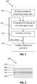
- FIG. 1 shows a flow chart illustrating subsequent process steps in a method according to the present invention.
- a substrate for example a substrate comprising an etch stack 200, 500
- lithography/etching is applied resulting in a metal-oxide 301 pattern.
- this pattern is shrunk in the thermally shrinking step 120.
- This thermal shrinking can be done in the lithography track.
- the cycle comprising the lithography/etching step 110 and the thermal shrinking step 120 is executed at least twice.
- thermal shrinking thus 120 can be done in the lithography track where the subsequent metal-oxide layer can be deposited.
- a thermal shrinking step 120 By subsequently executing a lithography/etching step 110 with a thermal shrinking step 120 and by executing this cycle at least twice, a smaller than litho-resolution structures can be obtained.
- a first metal-oxide pattern with reduced size is realized. The reduced size being realized by thermally shrinking the metal-oxide. Because of the reduced size of the the first metal-oxide pattern 302 it is possible to add, during the second cycle, a pattern of a thermally shrinkable metal-oxide 401 closer to the first metal-oxide pattern 302 than would be possible without the shrinking step.
- the overall metal-oxide pattern is, after the different cycles have been performed, transferred 140 into the bottom antireflective coating 220 and then into the amorphous carbon (a-C) layer 230 after executing the lithography/etching 110 and thermal shrinking 120 steps. This step is also illustrated in FIG. 1 .
- the process window can be enlarged by using different metal-oxides between the different cycles.
- the selectivity of the metal-oxide with regard to the etching means can be increased.
- the latter allows more variation of the process parameters, as the etching is performed selectively.
- the selectivity during each cycle must be realized by thermal treatment of the metal-oxides.
- the earlier shrunk blocks are made hard and etch resistant through the thermal treatment, such that these are not affected by the etch step used to pattern the subsequent block.
- an additional layer underlying the different metal oxide blocks is provided.
- the layer typically has similar n and k values as the photoresist, e.g. the photoresist on top of the BARC.
- the layer may for example be SiO 2 with dopants such as C, H and N for tuning the n and k values.
- Such an underlying layer thus may be an optically transparent layer for 193nm wavelength.
- a method is illustrated wherein a negative tone photoresist is used.
- an etch stack 200 is provided in a provision step.
- This stack (e.g. a 3xLE stack) comprises a target layer 250, covered by a hard mask 240, covered by an amorphous carbon (a-C, e.g. SiOC x ) layer 230 as the core layer, covered by a bottom antireflective coating 220, covered by a negative tone photo-resist 210.
- a-C e.g. SiOC x
- a lithography/etching step 110 In embodiments according to the present invention negative tone lithography exposure 311 is done and developed 312, resulting in a photo-resist layer 210 having a gap in the shape of the final required structure, but bigger in size than required.
- a spin-on metal-oxide layer 301 (also referred to as the memory layer) is deposited 313 over the resist layer thereby filling the gap in the photo-resist layer 210.
- the surface of the metal-oxide is planarized due to its spin-on deposition method.
- metal-oxide on top of the resist layer is etched 314, and the resist layer is etch-stripped 314 resulting in a pattern of thermally shrinkable metal-oxide 301.
- the metal-oxide on top of the resist layer may be etched using a dry etch step (e.g. using BCL 3 plasma), leaving behind metal-oxide material (memory block A) 301 in the gap of the resist layer.
- the lithography/etching step is followed by a shrinking step 120, thermally shrinking the metal-oxide 301 (the memory block A).
- the cycle of lithograpy/etching 110 and thermal shrinking 120 is repeated at least once.
- a new photo-resist layer 210 is applied, covering the shrunk memory block A.
- a lithography exposure 311 is done.
- development 312 of the photo-resist layer 210 a gap is achieved in the photo-resist layer. This gap is filled with metal-oxide in the metal-oxide spin on step 313.
- the photo-resist etch step 314, and after the thermal shrinking step 120 a new thermally shrunk pattern of metal-oxide is realized.
- FIG. 3 An example of a first cycle is shown in FIG. 3 . It shows a sequence of a litho exposure step 311, a litho development step 312, a metal-oxide spin on step 313, an etch back step of the metal-oxide and an photo-resist removal step 314 resulting in a memory block A 301.
- the photo-resist removal step is followed by a thermal shrinking step 120 resulting in a shrunk memory block A 302.
- FIG. 4 An example of a second cycle is shown in FIG. 4 .
- a litho exposure 311 step is done, followed by the same steps as in FIG.3 , resulting in a memory block B 401 which after thermal shrinking results in a shrunk memory block B 402.
- the cycle may be repeated 3 times, leaving memory blocks A (301, 302), B (401, 402), C (801, 802) shown in FIG. 11 .
- a method is illustrated wherein use is made of a positive tone photoresist.
- an etch stack 500 is provided in an additional step.
- This stack (e.g. a 3xLE stack) comprises, from the bottom target layer going up to the top resist layer, a bottom stack of target etch layer 250, covered by a hard mask layer 240 to do the final patterning, covered by an amorphous carbon (a-C, e.g. SiOC x ) layer 230 as the core layer, covered by a bottom antireflective coating 220, covered by a spin-on metal-oxide layer 301 (e.g.AlO x ), covered by a photoresist layer (210). An illustration thereof is shown in FIG. 5 .
- a-C e.g. SiOC x
- a spin-on metal-oxide layer 301 e.g.AlO x
- a lithography/etching step 110 In embodiments according to the present invention positive tone lithography exposure is done and developed. This leaves a photo-resist block 301 in the shape of the final required structure, but bigger in size than required.
- This photo-resist block may be transferred to the memory layer via dry etch 611 (e.g. using BCl 3 plasma for AlO x layer), creating the memory block A 301 corresponding to the first lithography mask-set. An exemplary embodiment thereof is shown in FIG. 6 .
- the lithography/etching step 110 is followed by a shrinking step 120, thermally shrinking the metal-oxide 301 by exposing the stack to thermal treatment, which shrinks the memory block A to the required size 302.
- An exemplary thermal shrinking step is illustrated as step 120 in FIG. 6 .
- the cycle of lithograpy/etching 110 and thermal shrinking 120 is repeated at least once.
- a 2nd memory layer using the same metal-oxide is spin-coated 711.
- the spin-coated metal-oxide layer thereby covers the already shrunk memory block A.
- An example thereof is shown in step 711 of FIG. 7 .
- the 2nd photoresist layer 210 is deposited 712 and the 2nd lithography exposure is done 713. After development of the photo-resist layer 210, the 2nd photo-resist block is achieved in the second photo-resist layer. An example thereof is shown in FIG. 7 .
- the 2nd photo-resist block is transferred 611 into the 2nd memory layer using a plasma chemistry to which shrunk memory block A 302 is selective (has lower etch rate).
- the plasma may be HBr plasma, in which AlO x before thermal shrink etches at the rate of 6nm/min while after thermal shrink it does not etch in HBr at all.
- memory block B 401 is created corresponding to the 2nd lithography mask-set.
- the lithography/etching step 110 is followed by a shrinking step 120, thermally shrinking the memory block B to the required size by exposing the stack to thermal treatment resulting in shrunk memory block B 402. Since memory block A has already shrunk during the shrinking step of the first cycle (step 120 illustrated in FIG. 6 ), it does not shrink further in this step.
- the cycle of lithograpy/etching 110 and thermal shrinking 120 is performed at least once, for example three times.
- a third cycle the whole process of 3rd spin-on memory layer deposition till 3rd memory block C shrink is followed exactly, following the above mentioned sequence comprising metal-oxide spin-on deposition 711, photo-resist deposition 712, lithography 713, litho etch into memory 611 and thermal shrinking 120.
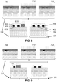
- FIG. 8 An example of these steps is illustrated in FIG. 8 in which the memory block C 801 and shrunk memory block C can be seen.
- a method is described using positive tone photoresist similar to the second example, but different metal-oxide layers are used in the different cycles.
- An etch stack 500 is provided during a provision step after which during a lithography/etching step 110 positive tone lithography exposure is done and developed resulting in a photo-resist block in the shape of the final required structure, but bigger in size than required.
- the photo-resist block is transferred to the memory layer via litho etching 611.
- the metal-oxide layer 301 may be an AlO x layer which may be etched using BCl 3 plasma. Thereby memory block A 301 is created corresponding to the first lithography mask-set. An exemplary embodiment thereof is shown in FIG. 6 .
- the lithography/etching step 110 is followed by a shrinking step 120, thermally shrinking the metal-oxide 301 by exposing the stack to thermal treatment, which shrinks the memory block A to the required size 302.
- An exemplary thermal shrinking step is illustrated as step 120 in FIG. 6 .
- the cycle of lithograpy/etching 110 and thermal shrinking 120 is repeated at least once.
- a 2nd memory layer using a second type of metal-oxide is spin-coated 711.
- An example thereof is shown in step 711 of FIG. 9 .
- the 2nd photoresist layer 210 is deposited 712 and the 2nd lithography exposure is done 713.
- the 2nd photo-resist block is achieved in the second photo-resist layer.
- FIG. 9 Next the 2nd photo-resist block is transferred 611 into the 2nd memory layer using a plasma chemistry to which shrunk memory block A 302 is selective (has lower etch rate).
- the plasma may be CF 4 plasma, in which the 2nd memory layer (TaO x ) before thermal shrink etches at up to 11 times faster (at an etch rate of 45nm/min) than shrunk memory block A 302 (AlO x ) which has been thermally shrunk (thermally treated at 550°C AlO x layer etches at 4nm/min). This creates memory block B 401 corresponding to the 2nd lithography mask-set.
- the lithography/etching step 110 is followed by a shrinking step 120, thermally shrinking the memory block B to the required size (shrunk memory block B 402) by exposing the stack to thermal treatment. Since shrunk memory block A 302 has already shrunk during the shrinking step of the first cycle (step 120 illustrated in FIG. 6 ), it does not shrink further in this step.
- the cycle of lithograpy/etching 110 and thermal shrinking 120 is performed at least once, for example three times.
- a third cycle the whole process of 3rd spin-on memory layer deposition till memory block C shrink is followed exactly, following the above mentioned sequence comprising metal-oxide spin-on deposition 711, photo-resist deposition 712, lithography 713, litho etch into memory 611 and thermal shrinking 120.
- An example of these steps is illustrated in FIG. 10 .
- the third metal-oxide may be different from the metal-oxide used in a previous cycle.
- the metal-oxide may for example be HfO x .
- the third photo-resist block transfer 611 to the 3rd memory layer can be done using Cl 2 based plasma etch (an example thereof is illustrated in FIG. 10 ). It is thereby an advantage of embodiments of the present invention that HfO 2 etches 3 times faster (at an etch rate of 36nm/min) than thermally shrunk TaO x and 5 times faster than thermally shrunk AlO x in Cl 2 plasma. This creates memory block C 801 corresponding to a 3rd lithography mask-set. An example of these steps is illustrated in FIG. 10 .
- the lithography/etching step 110 is followed by a shrinking step 120, thermally shrinking the memory block C to the required size (shrunk memory block C 802) by exposing the stack to thermal treatment. Since memory block A and B have already shrunk during the shrinking step of the first cycle and second cycle, they do not shrink further in this step.
- the metal-oxide pattern is transferred 140 into the bottom antireflective coating 220 and then into the amorphous carbon (a-C) layer.
- a-C amorphous carbon
- This may be done using a highly anisotropic O 2 based plasma etch which was the requirement of LE3x technique.
- An illustration thereof is shown in FIG. 11 .
- the left scheme shows 3 memory blocks on top of the BARC.
- the middle scheme shows the 3 memory blocks etched into the BARC.
- the right scheme shows the 3 memory blocks etched into the amorphous carbon layer.
- the shrinkage of different metal-oxides is controllable by heating the metal-oxide up to a certain temperature. This is illustrated in FIG. 12 .
- This figure shows for different metal-oxides (Al2O3, TaO2, Si-Ti oxide, HfO2) the normalized thickness after thermal treatment.
- metal-oxides Al2O3, TaO2, Si-Ti oxide, HfO2
- the left bar is the reference bar showing the normalized thickness of the metal-oxide before being submitted to thermal treatment.
- the middle bar shows the normalised thickness of the metal-oxide after thermal treatment at a temperature of 350°C
- the right bar shows the normalised thickness of the metal-oxide after thermal treatment at a temperature of 550°C.
- the shrink percentage of the metal-oxides can therefore be controlled by the temperature during thermal treatment. This temperature may be different for the different metal-oxides to obtain the desired shrink percentage.
- accurate aligning of the different blocks is performed.
- the latter may be done by using metal-oxide blocks being transparent to 193nm radiation.
- embodiments of the present invention relate to a chip made using a method in accordance with the present invention.
- the method 100 for patterning a substrate can be used to create cut and block masks for front end of line features (FEOL) in combination with spacer aligned quadruple patterning (SAQP) of the fins (in FinFET technology). It is thereby an advantage that they can be used at 22 nm and below.
- the method 100 for patterning a substrate can be used to create back end of line (BEOL) features, and again be used as cut/block mask for self-aligned double patterning (SADP) and SAQP.
- BEOL back end of line
- SADP self-aligned double patterning
Landscapes
- Physics & Mathematics (AREA)
- General Physics & Mathematics (AREA)
- Drying Of Semiconductors (AREA)
- Photosensitive Polymer And Photoresist Processing (AREA)
- Chemical & Material Sciences (AREA)
- Chemical Kinetics & Catalysis (AREA)
- General Chemical & Material Sciences (AREA)
- Manufacturing Of Printed Wiring (AREA)
Claims (14)
- Verfahren (100) zum lithografischen Mustern eines Substrats, wobei das Verfahren Folgendes umfasst:- Erhalten (130) eines Substrats, das zu mustern ist,- anschließend mindestens zweimaliges Anwenden des folgenden Zyklus:- Anwenden eines lithografischen Musterprozesses (110) einer wärmeschrumpfbaren Metalloxidschicht zum Bilden eines Metalloxidmusters, und Wärmeschrumpfen (120) des Metalloxidmusters,
wobei die unterschiedlichen Metalloxidmuster, die während der mindestens zwei Zyklen gebildet werden, in Bezug zueinander derart umrissen sind, dass die geschrumpften Metalloxidmuster gemeinsam ein Gesamtmuster bilden, das zu dem Substrat zu transferieren ist,- nach dem mindestens zweimaligen Anwenden des Zyklus, Transferieren (140) des Gesamtmusters zu dem Substrat. - Verfahren (100) nach Anspruch 1, wobei für aufeinanderfolgende Zyklen eine Temperatur, bei der das Wärmeschrumpfen des Metalloxidmusters ausgeführt wird, gleich oder niedriger ist als die Temperatur, bei der das Wärmeschrumpfen in früheren Zyklen ausgeführt wird.
- Verfahren (100) nach einem der vorhergehenden Ansprüche, wobei das verwendete Metalloxidmaterial in mindestens zwei der aufeinanderfolgenden angewandten Zyklen unterschiedlich ist.
- Verfahren (100) nach einem der vorhergehenden Ansprüche, wobei das Anwenden eines lithografischen Musterprozesses das Aufbringen eines Metalloxids unter Verwenden von Spin-Ablagerung (313) umfasst.
- Verfahren (100) nach einem der vorhergehenden Ansprüche, wobei das lithographische Mustern ein dreifacher Litho-Ätzprozess ist, wobei drei aufeinanderfolgende Zyklen lithografischen Musterns (110) und Wärmeschrumpfens (120) ausgeführt werden.
- Verfahren (100) nach Anspruch 5, wobei für jeden der drei aufeinanderfolgenden Zyklen ein unterschiedliches schrumpfbares Metalloxid verwendet wird, wobei jedes schrumpfbare Metalloxid eine kritische Temperatur für das Schrumpfen hat, und wobei in den drei aufeinanderfolgenden Zyklen jedes Mal eine Temperatur für das Schrumpfen verwendet wird, die höher ist als die kritische Temperatur für das Schrumpfen des Metalloxids, das in dem Zyklus verwendet wird, aber niedriger als die kritische Temperatur für das Schrumpfen von Metalloxid(en), das/die in den vorhergehenden Zyklen verwendet werden.
- Verfahren (100) nach einem der vorhergehenden Ansprüche, wobei das Umreißen der Metalloxidmuster in Bezug zueinander unter Berücksichtigung des Schrumpfens des Metalloxids ausgeführt wird, um Strukturen unter der minimalen Litho-Auflösung, die von dem lithografischen Prozess definiert wird, zu erhalten.
- Verfahren (100) nach einem der vorhergehenden Ansprüche, wobei während des Anwendens eines lithografischen Musterprozesses einer wärmeschrumpfbaren Metalloxidschicht ein Negative-Tone-Fotoresist verwendet wird, wobei Negative-Tone-Lithographieexposition ausgeführt wird.
- Verfahren nach Anspruch 8, wobei der lithografischen Musterprozess in mindestens einem Zyklus Folgendes umfasst:- Ablagern einer Negative-Tone-Fotoresistschicht,- Anwenden der Negative-Tone-Lithographieexposition (311) und Entwickeln (312) der Negative-Tone-Lithographie, das in einer Fotoresistschicht (210) resultiert, die eine Spalte hat,- Ablagern (313) der Metalloxidschicht (301) über der Resistschicht, wodurch die Spalte gefüllt wird,- Ätzen (314) des überschüssigen Metalloxids auf der Oberseite der Resistschicht, und- Ätz-Strippen der Resistschicht, das in dem Muster aus wärmeschrumpfbarem Metalloxid (301) resultiert.
- Verfahren (100) nach einem der vorhergehenden Ansprüche, wobei während des Anwendens eines lithografischen Musterprozesses einer wärmeschrumpfbaren Metalloxidschicht ein Positive-Tone-Fotoresist verwendet wird, wodurch Positive-Tone-Lithographieexposition ausgeführt wird.
- Verfahren (100) nach Anspruch 10, wobei der lithografische Musterprozess bei mindestens einem Zyklus Folgendes umfasst:- Ablagern der Metalloxidschicht,- Ablagern der Positive-Tone-Fotoresistschicht über der Metalloxidschicht,- Anwenden von Positive-Tone-Lithographieexposition, die in einer Fotoresist-Blockmaske resultiert,- Trockenätzen (611) des Fotoresistblocks, das in dem Mustern des wärmeschrumpfbaren Metalloxids resultiert.
- Verfahren (100) nach einem der vorhergehenden Ansprüche, wobei das Bereitstellen eines Substrats das Bereitstellen einer Zielschicht (250) umfasst, die durch eine harte Maske (240) abgedeckt ist, die durch eine amorphe Carbonschicht (230) abgedeckt ist und durch eine untere Reflexionsschutzbeschichtung (220) abgedeckt ist.
- Verfahren nach Anspruch 12, wobei das Verfahren das Transferieren (140) des Metalloxidmusters in die untere Reflexionsschutzbeschichtung (220) und dann in die amorphe Carbonschicht (230) umfasst.
- Chip, der unter Verwenden eines Verfahrens wie in einem der vorhergehenden Ansprüche beschrieben hergestellt wird.
Priority Applications (1)
| Application Number | Priority Date | Filing Date | Title |
|---|---|---|---|
| EP15201423.9A EP3035120B1 (de) | 2014-12-19 | 2015-12-18 | Verminderung der kritischen dimensionen in integrierten schaltungen |
Applications Claiming Priority (2)
| Application Number | Priority Date | Filing Date | Title |
|---|---|---|---|
| EP14199520 | 2014-12-19 | ||
| EP15201423.9A EP3035120B1 (de) | 2014-12-19 | 2015-12-18 | Verminderung der kritischen dimensionen in integrierten schaltungen |
Publications (3)
| Publication Number | Publication Date |
|---|---|
| EP3035120A2 EP3035120A2 (de) | 2016-06-22 |
| EP3035120A3 EP3035120A3 (de) | 2016-08-31 |
| EP3035120B1 true EP3035120B1 (de) | 2017-09-27 |
Family
ID=52144503
Family Applications (1)
| Application Number | Title | Priority Date | Filing Date |
|---|---|---|---|
| EP15201423.9A Active EP3035120B1 (de) | 2014-12-19 | 2015-12-18 | Verminderung der kritischen dimensionen in integrierten schaltungen |
Country Status (2)
| Country | Link |
|---|---|
| US (1) | US9406503B2 (de) |
| EP (1) | EP3035120B1 (de) |
Families Citing this family (6)
| Publication number | Priority date | Publication date | Assignee | Title |
|---|---|---|---|---|
| US9947548B2 (en) * | 2016-08-09 | 2018-04-17 | International Business Machines Corporation | Self-aligned single dummy fin cut with tight pitch |
| US11276572B2 (en) * | 2017-12-08 | 2022-03-15 | Tokyo Electron Limited | Technique for multi-patterning substrates |
| US11055464B2 (en) * | 2018-08-14 | 2021-07-06 | Taiwan Semiconductor Manufacturing Co., Ltd. | Critical dimension uniformity |
| CN111415860B (zh) * | 2019-01-07 | 2026-01-30 | 东京毅力科创株式会社 | 用于对基底进行多重图案化的方法 |
| US10985028B1 (en) | 2019-10-18 | 2021-04-20 | Taiwan Semiconductor Manufacturing Co., Ltd. | Semiconductor devices and methods of manufacturing |
| US12487523B2 (en) * | 2020-09-30 | 2025-12-02 | Taiwan Semiconductor Manufacturing Company, Ltd. | In-situ deposition and densification treatment for metal-comprising resist layer |
Family Cites Families (5)
| Publication number | Priority date | Publication date | Assignee | Title |
|---|---|---|---|---|
| US20040166447A1 (en) * | 2003-02-26 | 2004-08-26 | Vencent Chang | Method for shrinking pattern photoresist |
| US7696036B2 (en) * | 2007-06-14 | 2010-04-13 | International Business Machines Corporation | CMOS transistors with differential oxygen content high-k dielectrics |
| US20100213555A1 (en) * | 2009-02-23 | 2010-08-26 | Advanced Micro Devices, Inc. | Metal oxide semiconductor devices having capping layers and methods for fabricating the same |
| US8910095B2 (en) | 2013-02-19 | 2014-12-09 | Mentor Graphics Corporation | Layout decomposition for triple patterning lithography |
| US9177795B2 (en) * | 2013-09-27 | 2015-11-03 | Micron Technology, Inc. | Methods of forming nanostructures including metal oxides |
-
2015
- 2015-12-18 EP EP15201423.9A patent/EP3035120B1/de active Active
- 2015-12-21 US US14/977,146 patent/US9406503B2/en active Active
Non-Patent Citations (1)
| Title |
|---|
| None * |
Also Published As
| Publication number | Publication date |
|---|---|
| US20160181090A1 (en) | 2016-06-23 |
| EP3035120A3 (de) | 2016-08-31 |
| US9406503B2 (en) | 2016-08-02 |
| EP3035120A2 (de) | 2016-06-22 |
Similar Documents
| Publication | Publication Date | Title |
|---|---|---|
| US9406503B2 (en) | Decreasing the critical dimensions in integrated circuits | |
| US8883649B2 (en) | Sidewall image transfer process | |
| TWI505324B (zh) | 形成高密度圖案的方法 | |
| US9219007B2 (en) | Double self aligned via patterning | |
| US20200027735A1 (en) | Semiconductor structure and method for forming same | |
| US10079145B2 (en) | Method for pattern formation on a substrate, associated semiconductor devices, and uses of the method | |
| US9064813B2 (en) | Trench patterning with block first sidewall image transfer | |
| CN1256764C (zh) | 缩小间距的半导体元件的制造方法 | |
| US8883648B1 (en) | Manufacturing method of semiconductor structure | |
| US20180138078A1 (en) | Method for Regulating Hardmask Over-Etch for Multi-Patterning Processes | |
| CN104733322B (zh) | 用于制造多栅器件的鳍的方法和用于制造鳍的芯结构 | |
| US12185638B2 (en) | Metal/dielectric/metal hybrid hard mask to define ultra-large height top electrode for sub 60nm MRAM devices | |
| US12108679B2 (en) | Multiply spin-coated ultra-thick hybrid hard mask for sub 60nm MRAM devices | |
| US20130252425A1 (en) | Method of forming a semiconductor device | |
| US20180061658A1 (en) | Self-Aligned Patterning Process Utilizing Self-Aligned Blocking and Spacer Self-Healing | |
| CN104425567A (zh) | 提高钝化完整性的系统和方法 | |
| US10868244B2 (en) | Multiple hard mask patterning to fabricate 20nm and below MRAM devices | |
| JP2005294822A (ja) | 半導体デバイス製造方法および半導体構造 | |
| US6913958B1 (en) | Method for patterning a feature using a trimmed hardmask | |
| JP2002319573A (ja) | 半導体装置の製造方法 | |
| TWI621210B (zh) | 一種製作半導體元件的方法 | |
| TWI294652B (en) | Method for forming a gate structure and a conductive line structure | |
| JP2004228258A (ja) | 半導体装置の製造方法 | |
| KR100585866B1 (ko) | 반도체소자의 알루미늄 배선 형성방법 | |
| KR20080094403A (ko) | 반도체 소자의 하드마스크 형성 방법 및 이를 이용한 패턴형성 방법 |
Legal Events
| Date | Code | Title | Description |
|---|---|---|---|
| PUAI | Public reference made under article 153(3) epc to a published international application that has entered the european phase |
Free format text: ORIGINAL CODE: 0009012 |
|
| AK | Designated contracting states |
Kind code of ref document: A2 Designated state(s): AL AT BE BG CH CY CZ DE DK EE ES FI FR GB GR HR HU IE IS IT LI LT LU LV MC MK MT NL NO PL PT RO RS SE SI SK SM TR |
|
| AX | Request for extension of the european patent |
Extension state: BA ME |
|
| PUAL | Search report despatched |
Free format text: ORIGINAL CODE: 0009013 |
|
| AK | Designated contracting states |
Kind code of ref document: A3 Designated state(s): AL AT BE BG CH CY CZ DE DK EE ES FI FR GB GR HR HU IE IS IT LI LT LU LV MC MK MT NL NO PL PT RO RS SE SI SK SM TR |
|
| AX | Request for extension of the european patent |
Extension state: BA ME |
|
| RIC1 | Information provided on ipc code assigned before grant |
Ipc: G03F 7/00 20060101AFI20160722BHEP Ipc: G03F 7/40 20060101ALI20160722BHEP Ipc: H01L 21/00 20060101ALI20160722BHEP |
|
| STAA | Information on the status of an ep patent application or granted ep patent |
Free format text: STATUS: REQUEST FOR EXAMINATION WAS MADE |
|
| RBV | Designated contracting states (corrected) |
Designated state(s): AL AT BE BG CH CY CZ DE DK EE ES FI FR GB GR HR HU IE IS IT LI LT LU LV MC MK MT NL NO PL PT RO RS SE SI SK SM TR |
|
| 17P | Request for examination filed |
Effective date: 20170228 |
|
| GRAP | Despatch of communication of intention to grant a patent |
Free format text: ORIGINAL CODE: EPIDOSNIGR1 |
|
| STAA | Information on the status of an ep patent application or granted ep patent |
Free format text: STATUS: GRANT OF PATENT IS INTENDED |
|
| INTG | Intention to grant announced |
Effective date: 20170421 |
|
| GRAS | Grant fee paid |
Free format text: ORIGINAL CODE: EPIDOSNIGR3 |
|
| GRAA | (expected) grant |
Free format text: ORIGINAL CODE: 0009210 |
|
| STAA | Information on the status of an ep patent application or granted ep patent |
Free format text: STATUS: THE PATENT HAS BEEN GRANTED |
|
| AK | Designated contracting states |
Kind code of ref document: B1 Designated state(s): AL AT BE BG CH CY CZ DE DK EE ES FI FR GB GR HR HU IE IS IT LI LT LU LV MC MK MT NL NO PL PT RO RS SE SI SK SM TR |
|
| REG | Reference to a national code |
Ref country code: GB Ref legal event code: FG4D |
|
| REG | Reference to a national code |
Ref country code: CH Ref legal event code: EP |
|
| REG | Reference to a national code |
Ref country code: AT Ref legal event code: REF Ref document number: 932499 Country of ref document: AT Kind code of ref document: T Effective date: 20171015 |
|
| REG | Reference to a national code |
Ref country code: IE Ref legal event code: FG4D |
|
| REG | Reference to a national code |
Ref country code: DE Ref legal event code: R096 Ref document number: 602015005005 Country of ref document: DE |
|
| REG | Reference to a national code |
Ref country code: FR Ref legal event code: PLFP Year of fee payment: 3 |
|
| PG25 | Lapsed in a contracting state [announced via postgrant information from national office to epo] |
Ref country code: HR Free format text: LAPSE BECAUSE OF FAILURE TO SUBMIT A TRANSLATION OF THE DESCRIPTION OR TO PAY THE FEE WITHIN THE PRESCRIBED TIME-LIMIT Effective date: 20170927 Ref country code: SE Free format text: LAPSE BECAUSE OF FAILURE TO SUBMIT A TRANSLATION OF THE DESCRIPTION OR TO PAY THE FEE WITHIN THE PRESCRIBED TIME-LIMIT Effective date: 20170927 Ref country code: FI Free format text: LAPSE BECAUSE OF FAILURE TO SUBMIT A TRANSLATION OF THE DESCRIPTION OR TO PAY THE FEE WITHIN THE PRESCRIBED TIME-LIMIT Effective date: 20170927 Ref country code: NO Free format text: LAPSE BECAUSE OF FAILURE TO SUBMIT A TRANSLATION OF THE DESCRIPTION OR TO PAY THE FEE WITHIN THE PRESCRIBED TIME-LIMIT Effective date: 20171227 Ref country code: LT Free format text: LAPSE BECAUSE OF FAILURE TO SUBMIT A TRANSLATION OF THE DESCRIPTION OR TO PAY THE FEE WITHIN THE PRESCRIBED TIME-LIMIT Effective date: 20170927 |
|
| REG | Reference to a national code |
Ref country code: NL Ref legal event code: MP Effective date: 20170927 |
|
| REG | Reference to a national code |
Ref country code: LT Ref legal event code: MG4D |
|
| REG | Reference to a national code |
Ref country code: AT Ref legal event code: MK05 Ref document number: 932499 Country of ref document: AT Kind code of ref document: T Effective date: 20170927 |
|
| PG25 | Lapsed in a contracting state [announced via postgrant information from national office to epo] |
Ref country code: LV Free format text: LAPSE BECAUSE OF FAILURE TO SUBMIT A TRANSLATION OF THE DESCRIPTION OR TO PAY THE FEE WITHIN THE PRESCRIBED TIME-LIMIT Effective date: 20170927 Ref country code: GR Free format text: LAPSE BECAUSE OF FAILURE TO SUBMIT A TRANSLATION OF THE DESCRIPTION OR TO PAY THE FEE WITHIN THE PRESCRIBED TIME-LIMIT Effective date: 20171228 Ref country code: RS Free format text: LAPSE BECAUSE OF FAILURE TO SUBMIT A TRANSLATION OF THE DESCRIPTION OR TO PAY THE FEE WITHIN THE PRESCRIBED TIME-LIMIT Effective date: 20170927 Ref country code: BG Free format text: LAPSE BECAUSE OF FAILURE TO SUBMIT A TRANSLATION OF THE DESCRIPTION OR TO PAY THE FEE WITHIN THE PRESCRIBED TIME-LIMIT Effective date: 20171227 |
|
| PG25 | Lapsed in a contracting state [announced via postgrant information from national office to epo] |
Ref country code: NL Free format text: LAPSE BECAUSE OF FAILURE TO SUBMIT A TRANSLATION OF THE DESCRIPTION OR TO PAY THE FEE WITHIN THE PRESCRIBED TIME-LIMIT Effective date: 20170927 |
|
| PG25 | Lapsed in a contracting state [announced via postgrant information from national office to epo] |
Ref country code: ES Free format text: LAPSE BECAUSE OF FAILURE TO SUBMIT A TRANSLATION OF THE DESCRIPTION OR TO PAY THE FEE WITHIN THE PRESCRIBED TIME-LIMIT Effective date: 20170927 Ref country code: RO Free format text: LAPSE BECAUSE OF FAILURE TO SUBMIT A TRANSLATION OF THE DESCRIPTION OR TO PAY THE FEE WITHIN THE PRESCRIBED TIME-LIMIT Effective date: 20170927 Ref country code: CZ Free format text: LAPSE BECAUSE OF FAILURE TO SUBMIT A TRANSLATION OF THE DESCRIPTION OR TO PAY THE FEE WITHIN THE PRESCRIBED TIME-LIMIT Effective date: 20170927 |
|
| PG25 | Lapsed in a contracting state [announced via postgrant information from national office to epo] |
Ref country code: SM Free format text: LAPSE BECAUSE OF FAILURE TO SUBMIT A TRANSLATION OF THE DESCRIPTION OR TO PAY THE FEE WITHIN THE PRESCRIBED TIME-LIMIT Effective date: 20170927 Ref country code: EE Free format text: LAPSE BECAUSE OF FAILURE TO SUBMIT A TRANSLATION OF THE DESCRIPTION OR TO PAY THE FEE WITHIN THE PRESCRIBED TIME-LIMIT Effective date: 20170927 Ref country code: IT Free format text: LAPSE BECAUSE OF FAILURE TO SUBMIT A TRANSLATION OF THE DESCRIPTION OR TO PAY THE FEE WITHIN THE PRESCRIBED TIME-LIMIT Effective date: 20170927 Ref country code: IS Free format text: LAPSE BECAUSE OF FAILURE TO SUBMIT A TRANSLATION OF THE DESCRIPTION OR TO PAY THE FEE WITHIN THE PRESCRIBED TIME-LIMIT Effective date: 20180127 Ref country code: SK Free format text: LAPSE BECAUSE OF FAILURE TO SUBMIT A TRANSLATION OF THE DESCRIPTION OR TO PAY THE FEE WITHIN THE PRESCRIBED TIME-LIMIT Effective date: 20170927 Ref country code: AT Free format text: LAPSE BECAUSE OF FAILURE TO SUBMIT A TRANSLATION OF THE DESCRIPTION OR TO PAY THE FEE WITHIN THE PRESCRIBED TIME-LIMIT Effective date: 20170927 |
|
| REG | Reference to a national code |
Ref country code: DE Ref legal event code: R097 Ref document number: 602015005005 Country of ref document: DE |
|
| PG25 | Lapsed in a contracting state [announced via postgrant information from national office to epo] |
Ref country code: DK Free format text: LAPSE BECAUSE OF FAILURE TO SUBMIT A TRANSLATION OF THE DESCRIPTION OR TO PAY THE FEE WITHIN THE PRESCRIBED TIME-LIMIT Effective date: 20170927 |
|
| PLBE | No opposition filed within time limit |
Free format text: ORIGINAL CODE: 0009261 |
|
| STAA | Information on the status of an ep patent application or granted ep patent |
Free format text: STATUS: NO OPPOSITION FILED WITHIN TIME LIMIT |
|
| PG25 | Lapsed in a contracting state [announced via postgrant information from national office to epo] |
Ref country code: PL Free format text: LAPSE BECAUSE OF FAILURE TO SUBMIT A TRANSLATION OF THE DESCRIPTION OR TO PAY THE FEE WITHIN THE PRESCRIBED TIME-LIMIT Effective date: 20170927 |
|
| 26N | No opposition filed |
Effective date: 20180628 |
|
| REG | Reference to a national code |
Ref country code: IE Ref legal event code: MM4A |
|
| PG25 | Lapsed in a contracting state [announced via postgrant information from national office to epo] |
Ref country code: LU Free format text: LAPSE BECAUSE OF NON-PAYMENT OF DUE FEES Effective date: 20171218 Ref country code: MT Free format text: LAPSE BECAUSE OF NON-PAYMENT OF DUE FEES Effective date: 20171218 |
|
| REG | Reference to a national code |
Ref country code: BE Ref legal event code: MM Effective date: 20171231 |
|
| PG25 | Lapsed in a contracting state [announced via postgrant information from national office to epo] |
Ref country code: IE Free format text: LAPSE BECAUSE OF NON-PAYMENT OF DUE FEES Effective date: 20171218 |
|
| PG25 | Lapsed in a contracting state [announced via postgrant information from national office to epo] |
Ref country code: BE Free format text: LAPSE BECAUSE OF NON-PAYMENT OF DUE FEES Effective date: 20171231 Ref country code: SI Free format text: LAPSE BECAUSE OF FAILURE TO SUBMIT A TRANSLATION OF THE DESCRIPTION OR TO PAY THE FEE WITHIN THE PRESCRIBED TIME-LIMIT Effective date: 20170927 |
|
| PG25 | Lapsed in a contracting state [announced via postgrant information from national office to epo] |
Ref country code: HU Free format text: LAPSE BECAUSE OF FAILURE TO SUBMIT A TRANSLATION OF THE DESCRIPTION OR TO PAY THE FEE WITHIN THE PRESCRIBED TIME-LIMIT; INVALID AB INITIO Effective date: 20151218 Ref country code: MC Free format text: LAPSE BECAUSE OF FAILURE TO SUBMIT A TRANSLATION OF THE DESCRIPTION OR TO PAY THE FEE WITHIN THE PRESCRIBED TIME-LIMIT Effective date: 20170927 |
|
| REG | Reference to a national code |
Ref country code: CH Ref legal event code: PL |
|
| PG25 | Lapsed in a contracting state [announced via postgrant information from national office to epo] |
Ref country code: CY Free format text: LAPSE BECAUSE OF FAILURE TO SUBMIT A TRANSLATION OF THE DESCRIPTION OR TO PAY THE FEE WITHIN THE PRESCRIBED TIME-LIMIT Effective date: 20170927 |
|
| PG25 | Lapsed in a contracting state [announced via postgrant information from national office to epo] |
Ref country code: MK Free format text: LAPSE BECAUSE OF FAILURE TO SUBMIT A TRANSLATION OF THE DESCRIPTION OR TO PAY THE FEE WITHIN THE PRESCRIBED TIME-LIMIT Effective date: 20170927 |
|
| PG25 | Lapsed in a contracting state [announced via postgrant information from national office to epo] |
Ref country code: LI Free format text: LAPSE BECAUSE OF NON-PAYMENT OF DUE FEES Effective date: 20181231 Ref country code: CH Free format text: LAPSE BECAUSE OF NON-PAYMENT OF DUE FEES Effective date: 20181231 |
|
| PG25 | Lapsed in a contracting state [announced via postgrant information from national office to epo] |
Ref country code: TR Free format text: LAPSE BECAUSE OF FAILURE TO SUBMIT A TRANSLATION OF THE DESCRIPTION OR TO PAY THE FEE WITHIN THE PRESCRIBED TIME-LIMIT Effective date: 20170927 |
|
| PG25 | Lapsed in a contracting state [announced via postgrant information from national office to epo] |
Ref country code: PT Free format text: LAPSE BECAUSE OF FAILURE TO SUBMIT A TRANSLATION OF THE DESCRIPTION OR TO PAY THE FEE WITHIN THE PRESCRIBED TIME-LIMIT Effective date: 20170927 |
|
| PG25 | Lapsed in a contracting state [announced via postgrant information from national office to epo] |
Ref country code: AL Free format text: LAPSE BECAUSE OF FAILURE TO SUBMIT A TRANSLATION OF THE DESCRIPTION OR TO PAY THE FEE WITHIN THE PRESCRIBED TIME-LIMIT Effective date: 20170927 |
|
| GBPC | Gb: european patent ceased through non-payment of renewal fee |
Effective date: 20191218 |
|
| PG25 | Lapsed in a contracting state [announced via postgrant information from national office to epo] |
Ref country code: GB Free format text: LAPSE BECAUSE OF NON-PAYMENT OF DUE FEES Effective date: 20191218 |
|
| P01 | Opt-out of the competence of the unified patent court (upc) registered |
Effective date: 20230513 |
|
| PGFP | Annual fee paid to national office [announced via postgrant information from national office to epo] |
Ref country code: DE Payment date: 20251126 Year of fee payment: 11 |
|
| PGFP | Annual fee paid to national office [announced via postgrant information from national office to epo] |
Ref country code: FR Payment date: 20251120 Year of fee payment: 11 |