EP3032428A1 - Data communication device and method for data communication - Google Patents
Data communication device and method for data communication Download PDFInfo
- Publication number
- EP3032428A1 EP3032428A1 EP15199302.9A EP15199302A EP3032428A1 EP 3032428 A1 EP3032428 A1 EP 3032428A1 EP 15199302 A EP15199302 A EP 15199302A EP 3032428 A1 EP3032428 A1 EP 3032428A1
- Authority
- EP
- European Patent Office
- Prior art keywords
- signal
- terminal
- data
- clock
- slave unit
- Prior art date
- Legal status (The legal status is an assumption and is not a legal conclusion. Google has not performed a legal analysis and makes no representation as to the accuracy of the status listed.)
- Ceased
Links
Images




Classifications
-
- G—PHYSICS
- G06—COMPUTING OR CALCULATING; COUNTING
- G06F—ELECTRIC DIGITAL DATA PROCESSING
- G06F13/00—Interconnection of, or transfer of information or other signals between, memories, input/output devices or central processing units
- G06F13/38—Information transfer, e.g. on bus
- G06F13/42—Bus transfer protocol, e.g. handshake; Synchronisation
- G06F13/4282—Bus transfer protocol, e.g. handshake; Synchronisation on a serial bus, e.g. I2C bus, SPI bus
- G06F13/4291—Bus transfer protocol, e.g. handshake; Synchronisation on a serial bus, e.g. I2C bus, SPI bus using a clocked protocol
-
- G—PHYSICS
- G06—COMPUTING OR CALCULATING; COUNTING
- G06F—ELECTRIC DIGITAL DATA PROCESSING
- G06F13/00—Interconnection of, or transfer of information or other signals between, memories, input/output devices or central processing units
- G06F13/38—Information transfer, e.g. on bus
- G06F13/42—Bus transfer protocol, e.g. handshake; Synchronisation
- G06F13/4282—Bus transfer protocol, e.g. handshake; Synchronisation on a serial bus, e.g. I2C bus, SPI bus
-
- G—PHYSICS
- G06—COMPUTING OR CALCULATING; COUNTING
- G06F—ELECTRIC DIGITAL DATA PROCESSING
- G06F13/00—Interconnection of, or transfer of information or other signals between, memories, input/output devices or central processing units
- G06F13/14—Handling requests for interconnection or transfer
- G06F13/36—Handling requests for interconnection or transfer for access to common bus or bus system
- G06F13/362—Handling requests for interconnection or transfer for access to common bus or bus system with centralised access control
- G06F13/364—Handling requests for interconnection or transfer for access to common bus or bus system with centralised access control using independent requests or grants, e.g. using separated request and grant lines
-
- G—PHYSICS
- G06—COMPUTING OR CALCULATING; COUNTING
- G06F—ELECTRIC DIGITAL DATA PROCESSING
- G06F13/00—Interconnection of, or transfer of information or other signals between, memories, input/output devices or central processing units
- G06F13/38—Information transfer, e.g. on bus
- G06F13/40—Bus structure
- G06F13/4004—Coupling between buses
- G06F13/4027—Coupling between buses using bus bridges
- G06F13/404—Coupling between buses using bus bridges with address mapping
-
- G—PHYSICS
- G06—COMPUTING OR CALCULATING; COUNTING
- G06F—ELECTRIC DIGITAL DATA PROCESSING
- G06F13/00—Interconnection of, or transfer of information or other signals between, memories, input/output devices or central processing units
- G06F13/38—Information transfer, e.g. on bus
- G06F13/40—Bus structure
- G06F13/4063—Device-to-bus coupling
- G06F13/4068—Electrical coupling
Definitions
- the present invention generally relates to a data communication device, and more particularly to a data communication device that includes a master unit and a slave unit.
- Conventional data communication devices comprise a master unit and a slave unit (for example, see Patent Literature 1).
- Patent Literature 1 discloses that a communication interface device (data communication device) that comprises a central processing unit or CPU (master unit) and an interface circuit or IC (slave unit) that communicates with the CPU using a two-wire serial bus interface protocol.
- the CPU includes a terminal capable of outputting a data signal and a terminal capable of outputting a clock signal, and the terminals of the CPU input the data signal and the clock signal to the interface circuit. This makes the CPU and the interface circuit to communicate with each other using the two-wire serial bus interface protocol.
- Patent Literature 1 Japanese Patent Application Publication No. 2012-8982
- the communication interface device that comprises two interface circuits that have the same address (slave address) that makes the communication interface device to communicate using the two-wire serial bus interface protocol cannot use a terminal that outputs a data signal and a terminal that outputs a clock signal of the CPU to separate each control of the two interface circuits as common use. As a result, it is necessary to separate the terminal that outputs the data signal from the terminal that outputs the clock signal in the communication interface device. Thus, there are problems that the terminals of the CPU (master unit) cannot be efficiently used because the CPU needs to comprise an excess of a pair of terminals.
- a data communication device can control a plurality of slave units that have the same slave address, while using the terminals of the master unit efficiently.
- a data communication device may comprise a first slave unit; and a second slave unit that includes a slave address that is same as a slave address the first slave unit includes, wherein a data signal and a clock signal may be input to a data terminal and a clock terminal of one of the first slave unit and the second slave unit, respectively, a data signal and a clock signal may be input to a clock terminal and a data terminal of the other of the first slave unit and the second slave unit, respectively, and when the data signal and the clock signal is input to the clock terminal and the data terminal of the other of the first slave unit and the second slave unit, a level of the clock signal input to the data terminal may be detected when a signal level of the data signal input to the clock terminal changes.
- the data signal and the clock signal is input to the data terminal and the clock terminal of one of the first slave unit and the second slave unit, respectively. According to this, it may be possible to normally input the data signal and the clock signal that are output from the first terminal or the second terminal to the data terminal and the clock terminal. As a result, it may be possible to cause one of the first slave unit or the second slave unit to normally become a controllable condition. Furthermore, a data signal and a clock signal are input to a data terminal and a clock terminal of the other of the first slave unit and the second slave unit, respectively.
- the data signal and the clock signal are normally input to the data terminal and the clock terminal.
- the other of the first slave unit and the second slave unit it may be possible to cause the other of the first slave unit and the second slave unit to become an uncontrollable condition.
- the data communication device that comprises the master unit that includes the first terminal that outputs one of the data signal and the clock signal and the second terminal that outputs the other of the data signal and the clock signal
- the data communication device further comprises a master unit that comprises: a first terminal that outputs one of the data signal and the clock signal; and a second terminal that outputs the other of the data signal and the clock signal, wherein the master unit outputs the data signal and the clock signal to the data terminal and the clock terminal of a slave unit to be controlled between the first slave unit and the second slave unit, respectively.
- a master unit that comprises: a first terminal that outputs one of the data signal and the clock signal; and a second terminal that outputs the other of the data signal and the clock signal, wherein the master unit outputs the data signal and the clock signal to the data terminal and the clock terminal of a slave unit to be controlled between the first slave unit and the second slave unit, respectively.
- the first terminal of the master unit is connected to the data terminal of the first slave unit and the clock terminal of the second slave unit
- the second terminal of the master unit is connected to the clock terminal of the first slave unit and the data terminal of the second slave unit.
- the master unit outputs, to the data terminal and the clock terminal of the slave unit not to be controlled between the first slave unit and the second slave unit, the clock signal and the data signal, respectively, and a reference signal that includes a signal of at least one bit that is greater than or equal to a predetermined level, and a signal condition that is a stop condition is generated in the slave unit not to be controlled between the first slave unit and the second slave unit when the reference signal is input.
- the reference signal that includes the signal of at least one bit that is greater than or equal to the predetermined level enables to generate the signal condition that is the stop condition in the two-wire serial bus interface protocol.
- the reference signal may be a byte format signal that does not correspond to the slave address of the first slave unit and the second slave unit. According to this configuration, when the reference signal is the byte format, it may be possible to prevent matching the reference signal and the slave address of the first slave unit and the second slave unit. As a result, it may be possible to prevent the malfunction in the slave unit that is undesired to be controlled more precisely.
- the reference signal may be a signal of one bit that is greater than or equal to the predetermined level. According to this configuration, it may be possible to shorten time required for outputting the reference signal compared to a case that the reference signal is a byte (eight-bit) format because a signal of one bit that is greater than or equal to the predetermined level is only outputted.
- the data signal includes the reference signal, and a time period during which the signal of at least one bit that is greater than or equal to the predetermined level of the reference signal is longer than or equal to the predetermined level is greater than or equal to a time period during which the clock signal is greater than or equal to the predetermined level.
- the reference signal that includes the signal of at least one bit that is greater than or equal to the predetermined level can generate a signal condition that is a stop condition in the two-wire serial bus interface protocol.
- the reference signal is a signal that is periodically output at a time interval based on a number of bits of the slave address. According to this configuration, the reference signal can be precisely output before the malfunction occurs.
- a method for data communication comprises a step of inputting a data signal and a clock signal to a data terminal and a clock terminal of one of a first slave unit and a second slave unit that includes a slave address that is same as a slave address the first slave unit includes, respectively, and a data signal and a clock signal to a data terminal and a clock terminal of the other of the first slave unit and the second slave unit, respectively; and a step of detecting, when the data signal and the clock signal is input to the data terminal and the clock terminal of the other of the first slave unit and the second slave unit, a level of the clock signal input to the data terminal when a signal level of the data signal input to the clock terminal changes.
- the method for data communication comprises a step of inputting a data signal and a clock signal to a data terminal and a clock terminal of one of a first slave unit and a second slave unit that includes a slave address that is same as a slave address the first slave unit includes, respectively, and a data signal and a clock signal to a data terminal and a clock terminal of the other of the first slave unit and the second slave unit, respectively.
- the method for data communication comprises a step of outputting one of the data signal and the clock signal from a first terminal of a master unit, and the other of the data signal and the clock signal from a second terminal of the master unit, wherein the step of outputting the data signal and the clock signal from the master unit comprises a step of directly outputting the data signal and the clock signal to the data terminal and the clock terminal of a slave unit to be controlled from the master unit, respectively.
- the step of outputting the data signal and the clock signal from the master unit comprises a step of directly outputting the data signal and the clock signal to the data terminal and the clock terminal of a slave unit to be controlled from the master unit, respectively.
- the configuration that further comprises the master unit further comprises a step of outputting, from the master unit, a reference signal that includes a signal of at least one bit that is greater than or equal to a predetermined level; and a step of generating a stop condition in the slave unit not to be controlled between the first slave unit and the second slave unit when the reference signal is input.
- the reference signal that includes the signal of at least one bit that is greater than or equal to the predetermined level can generate a signal condition that is a stop condition in the two-wire serial bus interface protocol. Therefore, even if an effective signal is unintentionally generated in the slave unit that is undesired to be controlled, it may be possible to invalidate the effective generated signal. As a result, the malfunction in the slave unit that is undesired to be controlled can be easily prevented.
- a data communication device may comprise a first slave unit that comprises: a first data terminal that receives a data signal; and a first clock terminal that receives a clock signal; a second slave unit that comprises: a second data terminal that receives the clock signal; and a second clock terminal that receives the data signal, wherein the first salve unit and the second slave unit have a same slave address.
- the second slave unit may detect a level of the clock signal input to the second data terminal when a signal level of the data signal input to the second clock terminal changes.
- a data communication device may comprise a master unit comprising: a first master terminal that outputs one of a data signal and a clock signal; and a second master terminal that outputs the other of the data signal and the clock signal; and a first slave unit comprising: a first data terminal connected to the first master terminal, and a first clock terminal connected to the second master terminal, wherein the master unit is controlled based on the clock signal from the first master terminal and the data signal from the second master terminal.
- a method for data communication may comprise validating a data signal input to a first clock terminal of a first slave unit; inputting, to the first clock terminal, a reference signal; and invalidating the validated data signal.
- the data communication device can control a plurality of slave units that have the same slave address, while using the terminals of the master unit efficiently.
- the data communication device 100 may include a CPU 10, an IC 1, and an IC 2.
- the CPU 10 is connected to the IC 1 and the IC 2.
- the CPU 10 communicates with the IC 1 and the IC 2 based on a two-wire serial bus interface protocol (hereinafter, "two-wire type communication").
- the CPU 10 is an example of a "master unit”.
- the IC 1 and the IC 2 are a "first slave unit” and a "second slave unit", respectively (or, in some embodiments, the IC 1 and IC 2 may be the second slave unit and first slave unit, respectively).
- a receiver 101 that receives broadcast waves may include the data communication device 100.
- the CPU 10 is a controller that controls the entire receiver 101.
- the IC 1 and the IC 2 are an IC that includes a tuner function.
- the CPU 10 may include a terminal T1 and a terminal T2 to communicate with the IC 1 and the IC 2.
- the terminal T1 of the CPU 10 outputs one of a data signal and a clock signal.
- the terminal T2 of the CPU 10 outputs the other of the data signal and the clock signal, which is not output from the terminal T1.
- the terminal T1 and the terminal T2 are an example of a "first master terminal” and a "second master terminal", respectively.
- the IC 1 may include a data terminal dat 1 and a clock terminal clk 1.
- the IC 2 may include the data terminal dat 2 and the clock terminal clk 2.
- the data terminals dat 1 and dat 2 are terminals to which the data signal is input.
- the clock terminals clk 1 and clk 2 are terminals to which the clock signal is input.
- the IC 1 and the IC 2 have the same slave address (ID).
- ID the slave address
- both of the IC 1 and the IC 2 includes "0xC0" as the slave address.
- "0x" of "OxCO” indicates that alphanumeric characters following "0x” are represented as a hexadecimal number. That is, "OxCO” is represented as an eight-bit byte format such as "11000000".
- An eighth bit of the slave address represented as the eight-bit byte format is defined as a bit to designate WRITE/READ (WRITE/READ) mode in the two-wire type communication.
- the IC 1 and the IC 2 include two IC addresses for writing and reading, but to assist understanding, FIG. 1 shows the IC address for writing only.
- the IC 1 and the IC 2 may include the only slave address for either writing or reading.
- the terminal T 1 of the CPU 10 is connected to the data terminal dat 1 of the IC 1 and the clock terminal clk 2 of the IC 2 via wiring B1.
- the terminal T2 of the CPU 10 is connected to the clock terminal clk 1 of the IC 1 and the data terminal dat 2 of the IC 2 via the wiring B2.
- the CPU 10 when the CPU 10 controls the IC 1, the CPU 10 outputs the data signal from the terminal T1 and outputs the clock signal from the terminal T2.
- the CPU 10 controls the IC 2
- the CPU 10 outputs the clock signal from the terminal T1 and outputs the data signal from the terminal T2.
- the data signal and the clock signal are input to the data terminal dat 1 and the clock terminal clk 1 of the IC 1, respectively, and, on the other hand, the clock signal and the data signal are input to the data terminal dat 2 and the clock terminal clk 2 of the IC 2, respectively.
- the CPU 10 controls the IC 1 based on a detection of the data signal output from the terminal T1 that includes a signal corresponding to the slave address of the IC 1 the data terminals dat 1 and the clock terminal clk 2 may receive the data signal, and the clock terminal clk 1 and the data terminal dat 2 may receive the clock signal.
- the data signal and the clock signal are input to the data terminal dat 2 and the clock terminal clk 2 of the IC 2, and, on the other hand, the clock signal and the data signal are input to the data terminal dat 1 and the clock terminal clk 1 of the IC 1, respectively.
- the data terminal dat 2 and the clock terminal clk 1 may receive the data signal
- the clock terminal clk 2 and the data terminal dat 1 may receive the clock signal.
- the CPU 10 outputs the data signal and the clock signal to the data terminal and the clock terminal of the IC to be controlled between the IC 1 and the IC 2, respectively.
- the CPU 10 outputs the clock signal and the data signal to the data terminal and the clock terminal of the IC that is not controlled by the CPU 10, respectively.
- a program to perform the CPU 10 may control whether either one of the data signal or the clock signal is output from the terminals T1 and T2 of the CPU 10.
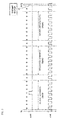
- FIG. 2 shows the signal input to the data terminal dat 1 and the clock terminal clk 1 of the IC 1.
- a pulse signal (clock signal) that includes predetermined frequency is input to the clock terminal clk 1.
- the CPU 10 First, at a time point t0, the CPU 10 generates a signal condition that is a start condition (*S) to start to control the IC 1.
- the start condition is issued to obtain bus usage rights before the CPU 10 starts to communicate.
- the start condition is also issued according to a procedure in which a serial data line (SDA) transitions from a high condition to a low condition when a serial clock line (SCL) is in the high condition.
- SDA serial data line
- SCL serial clock line
- the CPU 10 outputs an eight-bit signal corresponding to the slave address (0xC0) of the IC 1 as the data signal from the terminal T1 to the data terminal dat 1 during a period from a time point t1 to a time point t2. Then, when the signal corresponding to the slave address of the IC 1 itself is input to the IC 1, the IC 1 transits to the controllable condition and outputs an ACK signal ("A" shown in FIG. 2 ) to the CPU 10 during a period from a time point t2 to time point t3.
- the CPU 10 detects the ACK signal output from the IC 1, the CPU 10 acknowledges that a response to the signal corresponding to the slave address during the period from the time point t1 to the time point t2 is normally obtained, and then the CPU 10 is shifted to a next operation.
- the CPU 10 outputs a signal to designate a register address of the IC 1 as the data signal from the terminal T1 to the data terminal dat 1 during a period from a time point t3 to a time point t4.
- the register address is an address in which data is written (or read) in the IC 1.
- the eighth bit of the slave address represented as the eight-bit is defined as the bit to designate the WRITE/READ (WRITE/READ) mode in the two-wire type communication. Therefore, FIG. 2 shows a case that the WRITE (WRITE) mode is designated.
- the IC 1 when the signal to designate the register address to be written is normally input, the IC 1 outputs the ACK signal to the CPU 10 again during a period from a time point t4 to a time point t5.
- the CPU 10 detects the ACK signal output from the IC 1, the CPU 10 acknowledges that a response to the signal to designate the register address that is output during the period from the time point t3 to the time point t4 is normally obtained, and then the CPU 10 is shifted to a next operation.
- the CPU 10 outputs a signal corresponding to write data that is written in the designated resister address as the data signal from the terminal T1 to the data terminal dat 1 during a period from a time point t5 to a time point t6.
- the write data is represented as the eight-bit byte format like the slave address and the register address.
- the IC 1 outputs the ACK signal to the CPU 10 again during a period from a time point t6 to a time point t7.
- the CPU 10 detects the ACK signal output from the IC 1, the CPU 10 acknowledges that writing in the IC 1 is normally completed, and, at a time point t7, the CPU 10 generates the signal condition that is a stop condition (*P) to terminate to control the IC 1.
- the stop condition is issued to release a bus after data is transferred.
- the stop condition is also issued according to a procedure in which the SDA transitions to the low condition when the SCL is in the low condition, and then the SCL transitions to the high condition and the SDA transitions to the high condition.
- a start condition (*S)
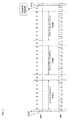
- FIG. 3 shows a signal input to the data terminal dat 2 and time point the clock terminal clk 2 of the IC 2.
- the CPU 10 outputs the data signal and the clock signal to the clock terminal clk 2 and the data terminal dat 2, respectively.
- a pulse signal (clock signal) that includes the predetermined frequency is input to the data terminal dat 2.
- the signal corresponding to the slave address (0xC0) of the IC 1 is input to the clock terminal clk 2 during the period from the time point t1 to the time point t2.
- the signal to designate the register address of the IC 1 is input to the clock terminal clk 2 during the period from the time point t3 to the time point t4.
- the signal corresponding to the write data that is written in the designated register address is input to the clock terminal clk 2 during the period from the time point t5 to the time point t6.
- the IC 2 detects a level of the clock signal input to the data terminal dat 2 as the signal condition that is the stop condition or the signal condition that is the start condition when the signal level of the data signal input to the clock terminal clk 2 changes.
- the IC 2 does become the controllable condition after the second the signal condition that is the start condition is generated, because the signal corresponding to the slave address (0xC0) of the IC 2 is not input.
- the IC 2 may detect a level of the clock signal input to the data terminal dat 2 when a signal level of the data signal input to the clock terminal clk 2 changes.
- the example that the CPU 10 controls the IC 1 is described above, but when the CPU 10 controls the IC 2, the data signal is input to the data terminal dat 2 of the IC 2 and the clock signal is input to the clock terminal clk 2, and the clock signal is input to the data terminal dat 1 of the IC 1 and the data signal is input to the clock terminal clk 1. Therefore, in such a case, the IC 2 becomes the controllable condition and the IC 1 does not become the controllable condition.
- the data signal and the clock signal are input to the data terminal dat 1 ( dat 2 ) and the clock terminal clk 1 (elk 2) of one of the IC 1 and the IC 2, respectively.
- This makes it possible to normally input the data signal and the clock signal that are output from the terminal T1 or the terminal T2 to the data terminal dat 1 (dat 2) and the clock terminal clk 1 (elk 2).
- it may be possible to cause one of the IC 1 and the IC 2 to normally become controllable condition.
- the clock signal and the data signal are input to the data terminal dat 1 (dat 2) and the clock terminal clk 1 (elk 2) of the other of the IC 1 and the IC 2, respectively.
- the data communication device 100 comprises the CPU 10 that includes the terminal T1 that output one of the data signal and the clock signal, and the terminal T2 that outputs the other one of the data signal and the clock signal
- the CPU 10 outputs the data signal and the clock signal to the data terminal and the clock terminal to be controlled between the IC 1 and the IC 2, respectively.
- the CPU 10 may output the data signal and the clock signal to the data terminal and the clock terminal to be controlled between the IC 1 and the IC 2, respectively.
- the terminal T1 of the CPU 10 is connected to the data terminal dat 1 of the IC 1 and the clock terminal clk 2 of the IC 2
- the terminal T2 of the CPU 10 is connected to the clock terminal clk 1 of the IC 1 and the data terminal dat 2 of the IC 2.
- FIGS. 4-10 embodiments of the second example will be described with reference to FIGS. 4-10 .
- an example that a malfunction may occur when a plurality of pairs of ICs that have the same slave address are controlled and an example of preventing the malfunction will be described.
- the description of the same configuration as one or more embodiments of the first example will be omitted.
- the data communication device 200 includes the CPU 110 and the ICs 3-8.
- the IC 3 and the IC 6 have the same slave address (0x00).
- the IC 4 and the IC 7 have the same slave address (0x08).
- the IC 5 and the IC 8 have the same slave address (0xFF).
- the CPU 110 is an example of the "master unit”.
- the IC 3, the IC 4, and the IC 5 are an example the "first slave unit”.
- the IC 6, the IC 7, and the IC 8 are an example of the "second slave unit".
- the ICs 3-8 include two IC addresses for writing and reading, but to assist understanding, FIG. 4 shows only one of the IC address for writing and the IC address for reading.
- the ICs 3-8 may include the only slave address for either writing or reading.
- the receiver 201 that receives the broadcast waves includes the data communication device 200.
- the CPU 110 is a controller that controls the entire receiver 201.
- the ICs 3 to 8 are the IC that includes the tuner function.
- the CPU 110 includes the terminals T11 and T12.
- the terminal T11 is connected to data terminals dat 3-5 of the ICs 3-5 and clock terminals clk 6-8 of the ICs 6-8 via a wiring B11.
- the terminal T12 is connected to the clock terminals clk 3-5 of the ICs 3-5 and the data terminals dat6-dat 8 of the ICs 6-8 via a wiring B12.
- the CPU 110 when the CPU 110 controls any of the ICs 3-5, the CPU 110 outputs the data signal from the terminal T11 and the clock signal from the terminal T12. Therefore, in this case, the data signal and the clock signal are input to the data terminals dat 3-5 and the clock terminals clk 3-5 of the ICs 3-5, respectively, and the clock signal and the data signal are input to the data terminals dat 6-8 and clock terminals clk 6-8 of the ICs 6-8, respectively.
- the CPU 110 controls any of the ICs 6-8
- the CPU 110 outputs the clock signal from the terminal T11 and the data signal from the terminal T12. Therefore, in this case, the data signal and the clock signal are input to the data terminals dat 6-8 and the clock terminals clk 6-8 of the ICs 6-8, respectively, and the clock signal and the data signal are input to the data terminals dat 3-5 and the clock terminals clk 3-5 of the ICs 3-5, respectively.
- a malfunction may occur in a special case.
- the special case that the malfunction may occur and a method for preventing the malfunction will be described below.
- the special case in which the malfunction may occur is a case where the following steps S 1-S3 may be followed.
- the IC 4 is controlled according to a predetermined procedure. Specifically, the CPU 110 outputs the following signal to the IC 4. As shown in FIG. 5 , the signal corresponding to the slave address (0x08) of the IC 4 is output. Next, the signal to designate the register address "0x00" is output. Then, the signal corresponding to the write data "0x00" is output.
- the IC 3 is controlled according to the predetermined procedure. Specifically, the CPU 110 outputs the following signal to the IC 3. As shown in FIG. 6 , first, the signal corresponding to the slave address (0x00) of the IC 3 is output. Next, the signal to designate the register address "0x00" is output. Then, the signal corresponding to the write data "0x00" is output.
- step S3 the control of the step S2 is repeated. As a result, the malfunction may occur.
- the input signal as shown in FIGS. 7 and 8 is the input signal at the steps S1 and S2 in view of the IC 8.
- the signal condition that is the start condition may be generated when the IC includes the high level bit (that is, the IC includes the slave address except for "0x00"), but not limited to, the slave address "0x08".
- the effective signal is not generated because a condition that the signal is not input to the clock terminal clk 4 of the IC 4 becomes.
- the pulse signal 21 does not cause to generate the signal conditions that are the start and stop conditions.
- the ICs above although actually performing the operations of the steps S1-S3 may be a rare case, one option is to take measures against the above malfunction in view of operating the data communication device 200 stably.
- the CPU 110 outputs an eight-bit byte format signal that includes the high level signal of at least one bit (hereinafter, "virtual ID") to prevent the malfunction. Furthermore, when the virtual ID is input, the IC that is not controlled among the ICs 3-5 and the ICs 6-8, that is, the IC to which the data signal and the clock signal are inverted and input causes the signal condition that is the stop condition to be generated. Furthermore, a period of the high level of the high level signal of at least one bit is longer than a period of the high level of the clock signal. Furthermore, the virtual ID is an example of the "reference signal".
- the high level signal included in the reference signal is an example of a "signal that is greater than or equal to the predetermined level".
- the low level signal may be a signal that is less than the predetermined level.
- a time period during which the reference signal is greater than or equal to the predetermined level may be longer than or equal to a time period during which the clock signal is greater than or equal to the predetermined level.
- the virtual ID is a byte format signal except for a byte format signal corresponding to the slave address of the ICs 3-8 connected to the CPU 110. That is, in the data communication device 200, the virtual ID is a byte format signal that is selected from "0x01-0x07" and "0x09-0xFE.” Furthermore, even if the IC that includes the slave address "0x00" such as the ICs 3 and 6 does not exist, "0x00" that does not include the high level signal may not be used as the virtual ID.
- the eighth bit of the slave address represented as an eight-bit is defined as a bit to designate the WRITE/READ (WRITE/READ) modes in the two-wire type communication, one option is not to use the signal corresponding to this as the virtual ID.
- the CPU 110 periodically outputs the virtual ID as the data signal in a state where the ICs 3-8 are not controlled. "Periodically" may be for every predetermined bytes or at predetermined intervals. Furthermore, it may be necessary to output the virtual ID at least before the malfunction occurs. For example, while the signal corresponding to the slave address is output eight times, it may be output the virtual ID at least once. That is, the virtual ID may be periodically output at a time interval based on a number of bits of the slave address. For example, the CPU 110 may count a number of outputting the slave address and the CPU 110 may output the virtual ID when the number of outputting the slave address achieves a predetermined number (e.g., eight times).
- a predetermined number e.g., eight times
- the pulse signal (clock signal) having the predetermined frequency is input to the data terminal dat 8. Furthermore, in the IC 8, the eight-bit signal as the virtual ID (0x02) is input to the clock terminal clk 8 during a period from a time point t21 to a time point t22.
- the signal condition that is the start condition may occur.
- the input of the next virtual ID may cause the effective high level signal to be invalidated.
- the data signal and the clock signal are input to the data terminals dat 3-5 (dat 6-8) and the clock terminals clk 3-5 (elk 6-8) of one of the ICs 3-5 and the ICs 6-8, respectively, and the clock signal and the data signal are input to the data terminals dat 3-5 (dat6-8) and the clock terminals clk 3-5 (elk 6-8) of the other of the ICs 3-5 and the ICs 6-8, respectively.
- the CPU 110 outputs the clock signal and the data signal to the data terminal and the clock terminal of the ICs that are not controlled among the ICs 3-5 and the ICs 6-8 IC, respectively, and the CPU 110 outputs the virtual ID that includes the high level signal of at least one bit so that the virtual ID is included in the data signal. Then, when the virtual ID is input (upon receiving the virtual ID), the IC that is not controlled among the ICs 3-5 and the ICs 6-8, that is, the IC to which the data signal and the clock signal are inverted and input causes the signal condition that is the stop condition to be generated.
- the virtual ID that includes the high level signal of at least one bit may generate the signal condition that is the stop condition in the two-wire serial bus interface protocol. Therefore, even if the effective signal is unintentionally generated in the IC 8 that is undesired to be controlled, it may be possible to invalidate the effective generated signal. As a result, the malfunction in the IC 8 that is undesired to be controlled can be easily prevented.
- the virtual ID may be the byte format signal except for the byte format signal corresponding to the slave address of the ICs 3-5 and ICs 6-8. According to this configuration, when the virtual ID is the byte format, it may be possible to prevent matching the virtual ID and the slave address of the ICs 3-5 and the ICs 6-8. As a result, it may be possible to prevent the malfunction in the IC 8 that is undesired to be controlled more precisely.
- the data signal includes the virtual ID. Furthermore, the period of the high level of the high level signal of one bit of the virtual ID is greater than the period of the high level of the clock signal. As a result, the virtual ID that includes the high level signal of at least one bit may generate the signal condition that is the stop condition in the two-wire serial bus interface protocol easily.
- the virtual ID may be the signal that is periodically output at the time interval based on a number of bits of the slave address. As a result, it may be possible to output the virtual ID precisely before the malfunction occurs.
- a data communication device 300 includes a CPU 210.
- the CPU 210 includes a terminal T11 and a terminal T12.
- the CPU 210 is connected to the ICs 3-8 by the connected condition like one or more embodiments of the second example.
- the CPU 210 is an example of the "master unit".
- a receiver 301 that receives the broadcast waves includes the data communication device 300.
- the CPU 210 is a controller that controls the entire receiver 301.
- the CPU 210 in one or more embodiments of the third example may control the ICs 3-8. Therefore, in the data communication device 300, the malfunction may occur in the special case like one or more embodiments of the second example.
- the CPU 210 outputs a high level bit format signal (hereinafter, "dummy bit") to prevent the malfunction. Furthermore, the CPU 210 periodically outputs the dummy bit as the data signal in a state where the ICs 3-8 are not controlled. Furthermore, the dummy bit is an example of the "reference signal”. Furthermore, the high level signal included in the dummy bit is an example of the "signal that is greater than or equal to the predetermined level". In this case, the low level signal may be the signal less than the predetermined level.
- the clock signal is input to the data terminal dat 8 and the data signal is input to the clock terminal clk 8.
- the dummy bit as the high level signal of one bit may generates the signal condition that is the stop condition (*P).
- the IC 8 acknowledges the effective high level signal, it may be possible to invalidate the effective high level signal.
- the dummy bit may be the high level signal of one bit.
- the dummy bit may be the high level signal of one bit.
- the examples of the data communication device 100 (200, 300) of the receiver 101 (201, 301) that receives the broadcast waves has been shown, but the present invention is not limited to the examples.
- One or more embodiments of the present invention may be applied to a data communication device of electronic apparatus except for the receiver.
- the first slave unit and the second slave unit are the ICs 1-8 that include the tuner function, but the present invention is not limited thereto.
- the first slave unit and the second slave unit may be all ICs that are controlled using the general two-wire type communication.
- the IC may be EEPROM.
- the master unit is the CPU 10 (110, 210), but the present invention is not limited thereto.
- the master unit may be a control circuit except for the CPU.
- the CPU 10 controls a pair of the IC 1 and the IC 2 that have the same slave address
- the second and third embodiments are illustrated where the CPU 110 (210) controls three pairs of a pair of the IC 3 and the IC 6, a pair of the IC 4 and the IC 7, and a pair of the IC 5 and the IC 8 that have the same slave address
- the CPU may control a pair of ICs that have the same slave address except for one or three same slave addresses.
- the terminal that outputs the data signal or the clock signal may be a pair of the terminal T1 (T11) and the terminal T2(T12) of the CPU 10 (110,210), but the present invention is not limited thereto.
- the terminal that outputs the data signal or the clock signal may be a plurality of pairs of terminals of the CPU.
- the virtual ID to prevent the malfunction is "0x02", but the present invention is not limited thereto.
- the virtual ID may be a byte format signal except for "0x02". In this case, as described above, it is necessary to use the virtual ID that is different from the slave address of the IC connected to the CPU and is a byte format signal except for "0x00".
Landscapes
- Engineering & Computer Science (AREA)
- Theoretical Computer Science (AREA)
- General Engineering & Computer Science (AREA)
- Physics & Mathematics (AREA)
- General Physics & Mathematics (AREA)
- Computer Hardware Design (AREA)
- Information Transfer Systems (AREA)
- Bus Control (AREA)
- Small-Scale Networks (AREA)
- Synchronisation In Digital Transmission Systems (AREA)
Abstract
Description
- The present invention generally relates to a data communication device, and more particularly to a data communication device that includes a master unit and a slave unit.
- Conventional data communication devices comprise a master unit and a slave unit (for example, see Patent Literature 1).
- The
aforementioned Patent Literature 1 discloses that a communication interface device (data communication device) that comprises a central processing unit or CPU (master unit) and an interface circuit or IC (slave unit) that communicates with the CPU using a two-wire serial bus interface protocol. In the communication interface device, the CPU includes a terminal capable of outputting a data signal and a terminal capable of outputting a clock signal, and the terminals of the CPU input the data signal and the clock signal to the interface circuit. This makes the CPU and the interface circuit to communicate with each other using the two-wire serial bus interface protocol. - [Patent Literature 1]
Japanese Patent Application Publication No. 2012-8982 - However, in the
aforementioned Patent Literature 1, for example, the communication interface device that comprises two interface circuits that have the same address (slave address) that makes the communication interface device to communicate using the two-wire serial bus interface protocol cannot use a terminal that outputs a data signal and a terminal that outputs a clock signal of the CPU to separate each control of the two interface circuits as common use. As a result, it is necessary to separate the terminal that outputs the data signal from the terminal that outputs the clock signal in the communication interface device. Thus, there are problems that the terminals of the CPU (master unit) cannot be efficiently used because the CPU needs to comprise an excess of a pair of terminals. - A data communication device according to one or more embodiments of the present invention can control a plurality of slave units that have the same slave address, while using the terminals of the master unit efficiently.
- A data communication device according to one or more embodiments of the present invention may comprise a first slave unit; and a second slave unit that includes a slave address that is same as a slave address the first slave unit includes, wherein a data signal and a clock signal may be input to a data terminal and a clock terminal of one of the first slave unit and the second slave unit, respectively, a data signal and a clock signal may be input to a clock terminal and a data terminal of the other of the first slave unit and the second slave unit, respectively, and when the data signal and the clock signal is input to the clock terminal and the data terminal of the other of the first slave unit and the second slave unit, a level of the clock signal input to the data terminal may be detected when a signal level of the data signal input to the clock terminal changes.
- In the data communication device according to one or more embodiments of the present invention, as described above, the data signal and the clock signal is input to the data terminal and the clock terminal of one of the first slave unit and the second slave unit, respectively. According to this, it may be possible to normally input the data signal and the clock signal that are output from the first terminal or the second terminal to the data terminal and the clock terminal. As a result, it may be possible to cause one of the first slave unit or the second slave unit to normally become a controllable condition. Furthermore, a data signal and a clock signal are input to a data terminal and a clock terminal of the other of the first slave unit and the second slave unit, respectively. According to this, in the other of the first slave unit and the second slave unit, the data signal and the clock signal are normally input to the data terminal and the clock terminal. As a result, it may be possible to cause the other of the first slave unit and the second slave unit to become an uncontrollable condition. Furthermore, in the data communication device that comprises the master unit that includes the first terminal that outputs one of the data signal and the clock signal and the second terminal that outputs the other of the data signal and the clock signal, it may be possible to cause the other of the first slave unit and the second slave unit to become the controllable condition and to cause one of the first slave unit and the second slave unit to become the uncontrollable condition by only switching a input condition of the data signal and the clock signal that are input to the first slave unit and the second slave unit, which are output from the first terminal or the second terminal. Thus, it may be possible to control the first slave unit and the second slave unit that have the same slave address separately by only using a pair of terminals that are the first terminal and the second terminal of the master unit. As a result, it may be possible to control a plurality of slave units that have the same slave address, while using the terminals of the master unit efficiently. As a result, it is necessary to separate the terminal that outputs the data signal from the terminal that outputs the clock signal in the communication interface device. Thus, there are problems that the terminals of the CPU (master unit) cannot be efficiently used because the CPU needs to comprise an excess of a pair of terminals.
- The data communication device according to one or more embodiments of the present invention further comprises a master unit that comprises: a first terminal that outputs one of the data signal and the clock signal; and a second terminal that outputs the other of the data signal and the clock signal, wherein the master unit outputs the data signal and the clock signal to the data terminal and the clock terminal of a slave unit to be controlled between the first slave unit and the second slave unit, respectively. According to this configuration, it may be possible to precisely control the slave unit to be controlled between the first slave unit and the second slave unit.
- In the configuration that further comprising the master unit, the first terminal of the master unit is connected to the data terminal of the first slave unit and the clock terminal of the second slave unit, and the second terminal of the master unit is connected to the clock terminal of the first slave unit and the data terminal of the second slave unit. According to this configuration, it may be possible to normally input the data signal and the clock signal that are output from the first terminal or the second terminal of the master unit to the data terminal and the clock terminal of one of the first slave unit and second slave unit easily. Furthermore, it becomes possible to cause the data signal and the clock signal not to be normally input to the data terminal and the clock terminal of the other of the first slave unit or the second slave unit easily.
- In the configuration that further comprising the master unit, the master unit outputs, to the data terminal and the clock terminal of the slave unit not to be controlled between the first slave unit and the second slave unit, the clock signal and the data signal, respectively, and a reference signal that includes a signal of at least one bit that is greater than or equal to a predetermined level, and a signal condition that is a stop condition is generated in the slave unit not to be controlled between the first slave unit and the second slave unit when the reference signal is input. According to this configuration, the reference signal that includes the signal of at least one bit that is greater than or equal to the predetermined level enables to generate the signal condition that is the stop condition in the two-wire serial bus interface protocol. Therefore, even if an effective signal is unintentionally generated in the slave unit that is undesired to be controlled, it may be possible to invalidate the effective generated signal. As a result, a malfunction in the slave unit that is undesired to be controlled can be easily prevented.
- In such a case, the reference signal may be a byte format signal that does not correspond to the slave address of the first slave unit and the second slave unit. According to this configuration, when the reference signal is the byte format, it may be possible to prevent matching the reference signal and the slave address of the first slave unit and the second slave unit. As a result, it may be possible to prevent the malfunction in the slave unit that is undesired to be controlled more precisely.
- In the configuration that outputs the reference signal, the reference signal may be a signal of one bit that is greater than or equal to the predetermined level. According to this configuration, it may be possible to shorten time required for outputting the reference signal compared to a case that the reference signal is a byte (eight-bit) format because a signal of one bit that is greater than or equal to the predetermined level is only outputted.
- In the configuration that outputs the reference signal, the data signal includes the reference signal, and a time period during which the signal of at least one bit that is greater than or equal to the predetermined level of the reference signal is longer than or equal to the predetermined level is greater than or equal to a time period during which the clock signal is greater than or equal to the predetermined level. According to this configuration, the reference signal that includes the signal of at least one bit that is greater than or equal to the predetermined level can generate a signal condition that is a stop condition in the two-wire serial bus interface protocol.
- In the configuration that outputs the reference signal, the reference signal is a signal that is periodically output at a time interval based on a number of bits of the slave address. According to this configuration, the reference signal can be precisely output before the malfunction occurs.
- A method for data communication according to one or more embodiments of the present invention comprises a step of inputting a data signal and a clock signal to a data terminal and a clock terminal of one of a first slave unit and a second slave unit that includes a slave address that is same as a slave address the first slave unit includes, respectively, and a data signal and a clock signal to a data terminal and a clock terminal of the other of the first slave unit and the second slave unit, respectively; and a step of detecting, when the data signal and the clock signal is input to the data terminal and the clock terminal of the other of the first slave unit and the second slave unit, a level of the clock signal input to the data terminal when a signal level of the data signal input to the clock terminal changes.
- The method for data communication according to one or more embodiments of the present invention, as described above, comprises a step of inputting a data signal and a clock signal to a data terminal and a clock terminal of one of a first slave unit and a second slave unit that includes a slave address that is same as a slave address the first slave unit includes, respectively, and a data signal and a clock signal to a data terminal and a clock terminal of the other of the first slave unit and the second slave unit, respectively. This makes it possible to control a plurality of slave units that have the same slave address, while using the terminals of the master unit efficiently, like the communication device according to the first aspect.
- The method for data communication according to one or more embodiments of the present invention comprises a step of outputting one of the data signal and the clock signal from a first terminal of a master unit, and the other of the data signal and the clock signal from a second terminal of the master unit, wherein the step of outputting the data signal and the clock signal from the master unit comprises a step of directly outputting the data signal and the clock signal to the data terminal and the clock terminal of a slave unit to be controlled from the master unit, respectively. According to this configuration, it may be possible to control the slave unit to be controlled between the first slave unit and the second slave unit.
- The configuration that further comprises the master unit further comprises a step of outputting, from the master unit, a reference signal that includes a signal of at least one bit that is greater than or equal to a predetermined level; and a step of generating a stop condition in the slave unit not to be controlled between the first slave unit and the second slave unit when the reference signal is input. According to this configuration, the reference signal that includes the signal of at least one bit that is greater than or equal to the predetermined level can generate a signal condition that is a stop condition in the two-wire serial bus interface protocol. Therefore, even if an effective signal is unintentionally generated in the slave unit that is undesired to be controlled, it may be possible to invalidate the effective generated signal. As a result, the malfunction in the slave unit that is undesired to be controlled can be easily prevented.
- A data communication device according to one or more embodiments of the present invention may comprise a first slave unit that comprises: a first data terminal that receives a data signal; and a first clock terminal that receives a clock signal; a second slave unit that comprises: a second data terminal that receives the clock signal; and a second clock terminal that receives the data signal, wherein the first salve unit and the second slave unit have a same slave address. In some embodiments, the second slave unit may detect a level of the clock signal input to the second data terminal when a signal level of the data signal input to the second clock terminal changes.
- A data communication device according to one or more embodiments of the present invention may comprise a master unit comprising: a first master terminal that outputs one of a data signal and a clock signal; and a second master terminal that outputs the other of the data signal and the clock signal; and a first slave unit comprising: a first data terminal connected to the first master terminal, and a first clock terminal connected to the second master terminal, wherein the master unit is controlled based on the clock signal from the first master terminal and the data signal from the second master terminal.
- A method for data communication according to one or more embodiments of the present invention may comprise validating a data signal input to a first clock terminal of a first slave unit; inputting, to the first clock terminal, a reference signal; and invalidating the validated data signal.
- According to one or more embodiments of the present invention, the data communication device can control a plurality of slave units that have the same slave address, while using the terminals of the master unit efficiently.
-
-
FIG. 1 is a diagram illustrating a configuration of a data communication device according to one or more embodiments of a first example of the present invention. -
FIG. 2 is a diagram illustrating an input signal in view of anIC 1 when theIC 1 is controlled in the data communication device according to one or more embodiments of the first example of the present invention. -
FIG. 3 is a diagram illustrating an input signal in view of an IC 2 when theIC 1 is controlled in the data communication device according to one or more embodiments of the first example of the present invention. -
FIG. 4 is a diagram illustrating a configuration of a data communication device according to one or more embodiments of second and third examples of the present invention. -
FIG. 5 is a diagram illustrating an input signal in view of anIC 4 when theIC 4 is controlled in the data communication device according to one or more embodiments of the second example of the present invention. -
FIG. 6 is a diagram illustrating an input signal in view of an IC 3 when the IC 3 is controlled in the data communication device according to one or more embodiments of the second example of the present invention. -
FIG. 7 is a diagram illustrating an input signal in view of an IC 8 when theIC 4 is controlled in the data communication device according to one or more embodiments of the second example of the present invention. -
FIG. 8 is a diagram illustrating an input signal in view of an IC 6-8 when the IC 3 is controlled in the data communication device according to one or more embodiments of the second example of the present invention. -
FIG. 9 is a diagram illustrating an input signal in view of the IC 3 when a virtual ID exists in the data communication device according to one or more embodiments of the second example of the present invention. -
FIG. 10 is a diagram illustrating an input signal in view of the IC 8 when a virtual ID exists in the data communication device according to one or more embodiments of the second example of the present invention. -
FIG. 11 is a diagram illustrating an input signal in view of the IC 8 when a dummy bit exists in the data communication device according to one or more embodiments of the third example of the present invention. - Embodiments of the present invention will be described in detail below, with reference to the drawings. In embodiments of the invention, numerous specific details are set forth in order to provide a more thorough understanding of the invention. However, it will be apparent to one of ordinary skill in the art that the invention may be practiced without these specific details. In other instances, well-known features have not been described in detail to avoid obscuring the invention.
- First, a configuration of a
data communication device 100 in accordance with one or more embodiments of the first example of the present invention will be described, with reference toFIG. 1 . - As shown in
FIG. 1 , thedata communication device 100 according to one or more embodiments of the first example of the present invention may include aCPU 10, anIC 1, and an IC 2. In thedata communication device 100, theCPU 10 is connected to theIC 1 and the IC 2. TheCPU 10 communicates with theIC 1 and the IC 2 based on a two-wire serial bus interface protocol (hereinafter, "two-wire type communication"). Furthermore, theCPU 10 is an example of a "master unit". TheIC 1 and the IC 2 are a "first slave unit" and a "second slave unit", respectively (or, in some embodiments, theIC 1 and IC 2 may be the second slave unit and first slave unit, respectively). - A
receiver 101 that receives broadcast waves may include thedata communication device 100. TheCPU 10 is a controller that controls theentire receiver 101. TheIC 1 and the IC 2 are an IC that includes a tuner function. - The
CPU 10 may include a terminal T1 and a terminal T2 to communicate with theIC 1 and the IC 2. The terminal T1 of theCPU 10 outputs one of a data signal and a clock signal. The terminal T2 of theCPU 10 outputs the other of the data signal and the clock signal, which is not output from the terminal T1. Furthermore, the terminal T1 and the terminal T2 are an example of a "first master terminal" and a "second master terminal", respectively. - The
IC 1 may include a data terminal dat 1 and aclock terminal clk 1. The IC 2 may include the data terminal dat 2 and the clock terminal clk 2. The data terminals dat 1 and dat 2 are terminals to which the data signal is input. The clock terminals clk 1 and clk 2 are terminals to which the clock signal is input. - The
IC 1 and the IC 2 have the same slave address (ID). For example, both of theIC 1 and the IC 2 includes "0xC0" as the slave address. Furthermore, "0x" of "OxCO" indicates that alphanumeric characters following "0x" are represented as a hexadecimal number. That is, "OxCO" is represented as an eight-bit byte format such as "11000000". - An eighth bit of the slave address represented as the eight-bit byte format is defined as a bit to designate WRITE/READ (WRITE/READ) mode in the two-wire type communication. Specifically, the eighth bit of the slave address that is a high level (=1) defines a READ mode. The eighth bit of the slave address that is a low level (=0) defines a WRITE mode. Therefore, in a case of the
IC 1 and the IC 2, when "0xC1 (=11000001)" is designated as the slave address, theIC 1 and the IC 2 enter the READ mode, and when "OxCO (=11000000)" is designated as the slave address, theIC 1 and the IC 2 enter the WRITE mode. Thus, theIC 1 and the IC 2 include two IC addresses for writing and reading, but to assist understanding,FIG. 1 shows the IC address for writing only. TheIC 1 and the IC 2 may include the only slave address for either writing or reading. - In one or more embodiments of the first example, the
terminal T 1 of theCPU 10 is connected to the data terminal dat 1 of theIC 1 and the clock terminal clk 2 of the IC 2 via wiring B1. The terminal T2 of theCPU 10 is connected to theclock terminal clk 1 of theIC 1 and the data terminal dat 2 of the IC 2 via the wiring B2. - In one or more embodiments of the first example, when the
CPU 10 controls theIC 1, theCPU 10 outputs the data signal from the terminal T1 and outputs the clock signal from the terminal T2. When theCPU 10 controls the IC 2, theCPU 10 outputs the clock signal from the terminal T1 and outputs the data signal from the terminal T2. - Therefore, in the
data communication device 100, when theCPU 10 controls theIC 1, the data signal and the clock signal are input to the data terminal dat 1 and theclock terminal clk 1 of theIC 1, respectively, and, on the other hand, the clock signal and the data signal are input to the data terminal dat 2 and the clock terminal clk 2 of the IC 2, respectively. Thus, when theCPU 10 controls theIC 1 based on a detection of the data signal output from the terminal T1 that includes a signal corresponding to the slave address of theIC 1, the data terminals dat 1 and the clock terminal clk 2 may receive the data signal, and theclock terminal clk 1 and the data terminal dat 2 may receive the clock signal. - When the
CPU 10 controls the IC 2, the data signal and the clock signal are input to the data terminal dat 2 and the clock terminal clk 2 of the IC 2, and, on the other hand, the clock signal and the data signal are input to the data terminal dat 1 and theclock terminal clk 1 of theIC 1, respectively. Thus, when the IC 2 is to be controlled by theCPU 10, the data terminal dat 2 and theclock terminal clk 1 may receive the data signal, and the clock terminal clk 2 and the data terminal dat 1 may receive the clock signal. - That is, the
CPU 10 outputs the data signal and the clock signal to the data terminal and the clock terminal of the IC to be controlled between theIC 1 and the IC 2, respectively. TheCPU 10 outputs the clock signal and the data signal to the data terminal and the clock terminal of the IC that is not controlled by theCPU 10, respectively. - Furthermore, a program to perform the
CPU 10 may control whether either one of the data signal or the clock signal is output from the terminals T1 and T2 of theCPU 10. - Next, control of the
IC 1 and the IC 2 by theCPU 10 will be described below with reference toFIGS. 2 and3 . Here, an example of a case that theCPU 10 controls theIC 1 will be described. - When the
IC 1 is controlled, theCPU 10 outputs the data signal and the clock signal to the data terminal dat 1 and theclock terminal clk 1 of theIC 1, respectively.FIG. 2 shows the signal input to the data terminal dat 1 and theclock terminal clk 1 of theIC 1. As shown inFIG. 2 , a pulse signal (clock signal) that includes predetermined frequency is input to theclock terminal clk 1. - First, at a time point t0, the
CPU 10 generates a signal condition that is a start condition (*S) to start to control theIC 1. The start condition is issued to obtain bus usage rights before theCPU 10 starts to communicate. The start condition is also issued according to a procedure in which a serial data line (SDA) transitions from a high condition to a low condition when a serial clock line (SCL) is in the high condition. For example, theCPU 10 generates the signal condition that is the start condition by decreasing the data signal from the high level (=1) to the low level (=0) in a state where the clock signal is the high level based on the protocol of the two-wire type communication. - Next, the
CPU 10 outputs an eight-bit signal corresponding to the slave address (0xC0) of theIC 1 as the data signal from the terminal T1 to the data terminal dat 1 during a period from a time point t1 to a time point t2. Then, when the signal corresponding to the slave address of theIC 1 itself is input to theIC 1, theIC 1 transits to the controllable condition and outputs an ACK signal ("A" shown inFIG. 2 ) to theCPU 10 during a period from a time point t2 to time point t3. - Then, when the
CPU 10 detects the ACK signal output from theIC 1, theCPU 10 acknowledges that a response to the signal corresponding to the slave address during the period from the time point t1 to the time point t2 is normally obtained, and then theCPU 10 is shifted to a next operation. - After that, the
CPU 10 outputs a signal to designate a register address of theIC 1 as the data signal from the terminal T1 to the data terminal dat 1 during a period from a time point t3 to a time point t4. The register address is an address in which data is written (or read) in theIC 1.FIG. 2 shows a case that 0x00 (=00000000) is designated as the register address, but practically a predetermined resister address may be designated. - As described above, the eighth bit of the slave address represented as the eight-bit is defined as the bit to designate the WRITE/READ (WRITE/READ) mode in the two-wire type communication. Therefore,
FIG. 2 shows a case that the WRITE (WRITE) mode is designated. - Turning back to
FIG. 2 , when the signal to designate the register address to be written is normally input, theIC 1 outputs the ACK signal to theCPU 10 again during a period from a time point t4 to a time point t5. - Next, the
CPU 10 detects the ACK signal output from theIC 1, theCPU 10 acknowledges that a response to the signal to designate the register address that is output during the period from the time point t3 to the time point t4 is normally obtained, and then theCPU 10 is shifted to a next operation. - Then, the
CPU 10 outputs a signal corresponding to write data that is written in the designated resister address as the data signal from the terminal T1 to the data terminal dat 1 during a period from a time point t5 to a time point t6. The write data is represented as the eight-bit byte format like the slave address and the register address.FIG. 2 shows a case that "0x00 (=00000000)" is designated as the write data, but practically, predetermined write data may be written. - Then, when the signal corresponding to the write data that is written in the designated register address is normally input, the
IC 1 outputs the ACK signal to theCPU 10 again during a period from a time point t6 to a time point t7. - After that, when the
CPU 10 detects the ACK signal output from theIC 1, theCPU 10 acknowledges that writing in theIC 1 is normally completed, and, at a time point t7, theCPU 10 generates the signal condition that is a stop condition (*P) to terminate to control theIC 1. The stop condition is issued to release a bus after data is transferred. The stop condition is also issued according to a procedure in which the SDA transitions to the low condition when the SCL is in the low condition, and then the SCL transitions to the high condition and the SDA transitions to the high condition. Specifically, theCPU 10 generates the signal condition that is the stop condition by increasing the data signal from the low level to the high level in a state where the clock signal is the high level based on the protocol of the two-wire type communication. As above, theCPU 10 controls theIC 1. Furthermore, the signal condition that is the start condition generated at the time point t8 is the signal condition that is the start condition for the next control. First, at a time point t0, theCPU 10 generates a signal condition that is a start condition (*S) to start to control theIC 1. Specifically, theCPU 10 generates the signal condition that is the start condition by decreasing the data signal from the high level to the low level (=0) based on the protocol of the two-wire type communication. - On the other hand,
FIG. 3 shows a signal input to the data terminal dat 2 and time point the clock terminal clk 2 of the IC 2. When theIC 1 is controlled, in the IC 2, theCPU 10 outputs the data signal and the clock signal to the clock terminal clk 2 and the data terminal dat 2, respectively. - As shown in
FIG. 3 , in the IC 2, a pulse signal (clock signal) that includes the predetermined frequency is input to the data terminal dat 2. On the other hand, in the IC 2, the signal corresponding to the slave address (0xC0) of theIC 1 is input to the clock terminal clk 2 during the period from the time point t1 to the time point t2. The signal to designate the register address of theIC 1 is input to the clock terminal clk 2 during the period from the time point t3 to the time point t4. The signal corresponding to the write data that is written in the designated register address is input to the clock terminal clk 2 during the period from the time point t5 to the time point t6. - In this case, in the IC 2, during the period from the time point t1 to the time point t2, each of the signal condition that is the start condition and the signal condition that is the stop condition is generated twice in response to a high level signal of two bits (signal corresponding to the first two-bits "11") among the eight-bit signal corresponding to the slave address (0xC0=11000000) of the
IC 1. In other words, the IC 2 detects a level of the clock signal input to the data terminal dat 2 as the signal condition that is the stop condition or the signal condition that is the start condition when the signal level of the data signal input to the clock terminal clk 2 changes. On the other hand, the IC 2 does become the controllable condition after the second the signal condition that is the start condition is generated, because the signal corresponding to the slave address (0xC0) of the IC 2 is not input. Thus, if the clock terminal clk 2 and the data terminal dat 2 receive the data signal and the clock signal, respectively, the IC 2 may detect a level of the clock signal input to the data terminal dat 2 when a signal level of the data signal input to the clock terminal clk 2 changes. - Furthermore, the example that the
CPU 10 controls theIC 1 is described above, but when theCPU 10 controls the IC 2, the data signal is input to the data terminal dat 2 of the IC 2 and the clock signal is input to the clock terminal clk 2, and the clock signal is input to the data terminal dat 1 of theIC 1 and the data signal is input to theclock terminal clk 1. Therefore, in such a case, the IC 2 becomes the controllable condition and theIC 1 does not become the controllable condition. - According to one or more embodiments of the first example, one or more of the following effects can be obtained.
- In one or more embodiments of the first example, as described above, the data signal and the clock signal are input to the data terminal dat 1 ( dat 2 ) and the clock terminal clk 1 (elk 2) of one of the
IC 1 and the IC 2, respectively. This makes it possible to normally input the data signal and the clock signal that are output from the terminal T1 or the terminal T2 to the data terminal dat 1 (dat 2) and the clock terminal clk 1 (elk 2). As a result, it may be possible to cause one of theIC 1 and the IC 2 to normally become controllable condition. Furthermore, the clock signal and the data signal are input to the data terminal dat 1 (dat 2) and the clock terminal clk 1 (elk 2) of the other of theIC 1 and the IC 2, respectively. This makes it possible not to normally input the data signal and the clock signal to data terminal dat 1 (dat 2) and clock terminal clk 1 (elk 2) to the other of theIC 1 and the IC 2. As a result, it may be possible to cause the other of theIC 1 and the IC 2 to become the uncontrollable condition. Furthermore, when thedata communication device 100 comprises theCPU 10 that includes the terminal T1 that output one of the data signal and the clock signal, and the terminal T2 that outputs the other one of the data signal and the clock signal, it may be possible to cause the other of theIC 1 and the IC 2 to become the controllable condition and cause one of theIC 1 and the IC 2 to become the uncontrollable condition by only switching an input condition of the data signal and the clock signal that are input to theIC 1 and the IC 2, which are output from the terminal T1 or the terminal T2. As a result, it may be possible to control a plurality of ICs that have the same slave address, while using the terminals of theCPU 10 efficiently, because it may be possible to control theIC 1 and the IC 2 that have the same slave address separately by only using a pair of the terminal T1 and the terminal T2 of theCPU 10. - Furthermore, according to one or more embodiments of the first example, as described above, the
CPU 10 outputs the data signal and the clock signal to the data terminal and the clock terminal to be controlled between theIC 1 and the IC 2, respectively. As a result, it may be possible to control the IC to be controlled between theIC 1 and the IC 2 precisely. - Furthermore, according to one or more embodiments of the first example, as described above, the terminal T1 of the
CPU 10 is connected to the data terminal dat 1 of theIC 1 and the clock terminal clk 2 of the IC 2, and the terminal T2 of theCPU 10 is connected to theclock terminal clk 1 of theIC 1 and the data terminal dat 2 of the IC 2. As a result, it may be possible to normally input the data signal and the clock signal that are output the terminal T1 or the terminal T2 of theCPU 10 to the data terminal dat 1 ( dat 2 ) and the clock terminal clk 1 (elk 2) of one of theIC 1 and the IC 2 easily. Furthermore, it may be possible to prevent to normally input the data signal and the clock signal to the data terminal dat 1 (dat 2) and the clock terminal clk 1 (elk 2) of the other of theIC 1 and the IC 2 easily. - Next, embodiments of the second example will be described with reference to
FIGS. 4-10 . In one or more embodiments of the second example, an example that a malfunction may occur when a plurality of pairs of ICs that have the same slave address are controlled and an example of preventing the malfunction will be described. Furthermore, the description of the same configuration as one or more embodiments of the first example will be omitted. - As shown in
FIG. 4 , thedata communication device 200 according to one or more embodiments of the second example of the present invention includes the CPU 110 and the ICs 3-8. In thedata communication device 200, the IC 3 and the IC 6 have the same slave address (0x00). Furthermore, theIC 4 and the IC 7 have the same slave address (0x08). Furthermore, the IC 5 and the IC 8 have the same slave address (0xFF). Furthermore, the CPU 110 is an example of the "master unit". Furthermore, the IC 3, theIC 4, and the IC 5 are an example the "first slave unit". Furthermore, the IC 6, the IC 7, and the IC 8 are an example of the "second slave unit". - Furthermore, in one or more embodiments of the second example like one or more embodiments of the first example, the ICs 3-8 include two IC addresses for writing and reading, but to assist understanding,
FIG. 4 shows only one of the IC address for writing and the IC address for reading. The ICs 3-8 may include the only slave address for either writing or reading. - The
receiver 201 that receives the broadcast waves includes thedata communication device 200. The CPU 110 is a controller that controls theentire receiver 201. The ICs 3 to 8 are the IC that includes the tuner function. - The CPU 110 includes the terminals T11 and T12. The terminal T11 is connected to data terminals dat 3-5 of the ICs 3-5 and clock terminals clk 6-8 of the ICs 6-8 via a wiring B11. The terminal T12 is connected to the clock terminals clk 3-5 of the ICs 3-5 and the data terminals dat6-dat 8 of the ICs 6-8 via a wiring B12.
- In one or more embodiments of the second example, when the CPU 110 controls any of the ICs 3-5, the CPU 110 outputs the data signal from the terminal T11 and the clock signal from the terminal T12. Therefore, in this case, the data signal and the clock signal are input to the data terminals dat 3-5 and the clock terminals clk 3-5 of the ICs 3-5, respectively, and the clock signal and the data signal are input to the data terminals dat 6-8 and clock terminals clk 6-8 of the ICs 6-8, respectively.
- Furthermore, when the CPU 110 controls any of the ICs 6-8, the CPU 110 outputs the clock signal from the terminal T11 and the data signal from the terminal T12. Therefore, in this case, the data signal and the clock signal are input to the data terminals dat 6-8 and the clock terminals clk 6-8 of the ICs 6-8, respectively, and the clock signal and the data signal are input to the data terminals dat 3-5 and the clock terminals clk 3-5 of the ICs 3-5, respectively.
- Like the
data communication device 200, when the CPU 110 controls a plurality of pairs of ICs that have the same slave address (three pairs of a pair of the IC 3 and the IC 6, a pair of theIC 4 and the IC 7, and a pair of the IC 5 and the IC 8), a malfunction may occur in a special case. The special case that the malfunction may occur and a method for preventing the malfunction will be described below. - Specifically, the special case in which the malfunction may occur is a case where the following steps S 1-S3 may be followed.
- First, at a step S1, the
IC 4 is controlled according to a predetermined procedure. Specifically, the CPU 110 outputs the following signal to theIC 4. As shown inFIG. 5 , the signal corresponding to the slave address (0x08) of theIC 4 is output. Next, the signal to designate the register address "0x00" is output. Then, the signal corresponding to the write data "0x00" is output. - At the step S2, the IC 3 is controlled according to the predetermined procedure. Specifically, the CPU 110 outputs the following signal to the IC 3. As shown in
FIG. 6 , first, the signal corresponding to the slave address (0x00) of the IC 3 is output. Next, the signal to designate the register address "0x00" is output. Then, the signal corresponding to the write data "0x00" is output. - At the step S3, the control of the step S2 is repeated. As a result, the malfunction may occur.
- The input signal as shown in
FIGS. 7 and8 is the input signal at the steps S1 and S2 in view of the IC 8. First, as shown inFIG. 7 , a high level signal of one bit (signal of a fifth bit) among the eight-bit signal corresponding to the slave address (0x08=00001000) of theIC 4 at the step S1 causes to generate the signal condition that is the start condition (*S) at a time point t11. Furthermore, the signal condition that is the start condition may be generated when the IC includes the high level bit (that is, the IC includes the slave address except for "0x00"), but not limited to, the slave address "0x08". - Furthermore, during a period corresponding to the register address "0x00" and the write data "0x00", the effective signal is not generated because a condition that the signal is not input to the
clock terminal clk 4 of theIC 4 becomes. Afterwards, the IC 8 acknowledges the effective high level (=1) signal by apulse signal 21 to terminate the control of theIC 4 at the step S1 (and to start the control of the IC 3 as shown inFIG. 8 ). Furthermore, because a pulse width of thepulse signal 21 is narrower than a pulse width of the clock signal, thepulse signal 21 does not cause to generate the signal conditions that are the start and stop conditions. - Next, as shown in
FIG. 8 , at the step S2, the high level signal does not exist because the eight-bit signals corresponding to the slave address of the IC 3, the register address, and write data are "0x00 (=00000000)." Therefore, in the IC 8, the signal condition that is the stop condition does not occur. Furthermore, the IC 8 acknowledges the effective high level (=1) signal by apulse signal 22 to terminate the control of the IC 3 at the step S2 (and to start the next control of the IC 3). In this case, because the signal condition that is the stop condition is not generated during a period from thepulse signal 21 at thestep S 1 to thepulse signal 22 at the step S2, the IC 8 acknowledges thepulse signal 21 and thepulse signal 22 as a continuous signal. - Then, by repeating the processing of the step S2 at the step S3, the IC 8 continues to acknowledge the effective high level (=1) signal by repeating the
pulse signal 22 to terminate the control of the IC 3 in a state where the signal condition that is the stop condition is not generated in the IC 8. When the IC 8 acknowledges the effective high level signals eight times, the IC 8 acknowledges the slave address (0xFF= 11111111) of the IC 8 itself is normally input, and, as a result, the malfunction may occur. In the combination of the ICs above, although actually performing the operations of the steps S1-S3 may be a rare case, one option is to take measures against the above malfunction in view of operating thedata communication device 200 stably. - In one or more embodiments of the second example, the CPU 110 outputs an eight-bit byte format signal that includes the high level signal of at least one bit (hereinafter, "virtual ID") to prevent the malfunction. Furthermore, when the virtual ID is input, the IC that is not controlled among the ICs 3-5 and the ICs 6-8, that is, the IC to which the data signal and the clock signal are inverted and input causes the signal condition that is the stop condition to be generated. Furthermore, a period of the high level of the high level signal of at least one bit is longer than a period of the high level of the clock signal. Furthermore, the virtual ID is an example of the "reference signal". Furthermore, the high level signal included in the reference signal is an example of a "signal that is greater than or equal to the predetermined level". In this case, the low level signal may be a signal that is less than the predetermined level. Thus, a time period during which the reference signal is greater than or equal to the predetermined level may be longer than or equal to a time period during which the clock signal is greater than or equal to the predetermined level.
- The virtual ID is a byte format signal except for a byte format signal corresponding to the slave address of the ICs 3-8 connected to the CPU 110. That is, in the
data communication device 200, the virtual ID is a byte format signal that is selected from "0x01-0x07" and "0x09-0xFE." Furthermore, even if the IC that includes the slave address "0x00" such as the ICs 3 and 6 does not exist, "0x00" that does not include the high level signal may not be used as the virtual ID. - Furthermore, as described above, because the eighth bit of the slave address represented as an eight-bit is defined as a bit to designate the WRITE/READ (WRITE/READ) modes in the two-wire type communication, one option is not to use the signal corresponding to this as the virtual ID. Specifically, the IC includes the two slave addresses for writing and reading, for example, the IC includes "0x08(=00001000)" and "0x09(=00001001)", one option is not to use the two addresses as the virtual ID. Furthermore, when the IC includes any of the slave address for writing and the slave address for reading, for example, the IC includes "0x08(=00001000)" only or "0x09(=00001001)" only, one option is not to use the slave address that is one of "0x08" and "0x09" as the virtual ID and it may be possible to use the slave address the other as the virtual ID.
- Furthermore, the CPU 110 periodically outputs the virtual ID as the data signal in a state where the ICs 3-8 are not controlled. "Periodically" may be for every predetermined bytes or at predetermined intervals. Furthermore, it may be necessary to output the virtual ID at least before the malfunction occurs. For example, while the signal corresponding to the slave address is output eight times, it may be output the virtual ID at least once. That is, the virtual ID may be periodically output at a time interval based on a number of bits of the slave address. For example, the CPU 110 may count a number of outputting the slave address and the CPU 110 may output the virtual ID when the number of outputting the slave address achieves a predetermined number (e.g., eight times).
- Next, preventing the malfunction in the special case using the virtual ID will be described with reference to
FIGS. 9 and10 . A case that "0x02" is used as the virtual ID will be described. Furthermore, an example of an input signal in view of the ICs 3 and 8 will be described. - As shown in
FIG. 9 , the CPU 110 outputs the eight-bit signal (0x02=00000010) of the data signal as the data signal to the data terminal dat 3 of the data signal during a period from a time point t21 to a time point t22. Furthermore, the pulse signal (clock signal) having the predetermined frequency from the terminal T12 of the CPU 110 to the clock terminal clk 3 of the IC 3. - On the other hand, as shown in
FIG. 10 , in the IC 8, the pulse signal (clock signal) having the predetermined frequency is input to the data terminal dat 8. Furthermore, in the IC 8, the eight-bit signal as the virtual ID (0x02) is input to the clock terminal clk 8 during a period from a time point t21 to a time point t22. - In this case, a high level signal of one bit (signal of the second bit) among the eight-bit signal corresponding to the virtual ID(0x02=00000010 may cause the signal condition that is the stop condition (*P) to be occurred at a time point t23. As a result, even if the IC 8 acknowledges the effective high level signal, it may be possible to invalidate the effective high level signal. Furthermore, after the invalidation, the signal condition that is the start condition may occur. However, even if the effective high level signal occurs after the signal condition that is the start condition, the input of the next virtual ID may cause the effective high level signal to be invalidated.
- Furthermore, other configurations of one or more embodiments of the second example are similar to configurations of one or more embodiments of the first example.
- According to one or more embodiments of the second example, one or more of the following effects can be obtained.
- In one or more embodiments of the second example, as described above, the data signal and the clock signal are input to the data terminals dat 3-5 (dat 6-8) and the clock terminals clk 3-5 (elk 6-8) of one of the ICs 3-5 and the ICs 6-8, respectively, and the clock signal and the data signal are input to the data terminals dat 3-5 (dat6-8) and the clock terminals clk 3-5 (elk 6-8) of the other of the ICs 3-5 and the ICs 6-8, respectively. As a result, like one or more embodiments of the first example, because it is possible to control a pair of the IC 3 and the IC 6, a pair of the
IC 4 and the IC 7, and a pair of the IC 5 and the IC 8 that includes the same slave address using a pair of terminals of the terminal T11 and the terminal T12 of the CPU 110 only, it may be possible to a plurality of ICs that includes the same slave address, while using the terminals of the CPU 110 efficiently. - Furthermore, in one or more embodiments of the second example, as described above, the CPU 110 outputs the clock signal and the data signal to the data terminal and the clock terminal of the ICs that are not controlled among the ICs 3-5 and the ICs 6-8 IC, respectively, and the CPU 110 outputs the virtual ID that includes the high level signal of at least one bit so that the virtual ID is included in the data signal. Then, when the virtual ID is input (upon receiving the virtual ID), the IC that is not controlled among the ICs 3-5 and the ICs 6-8, that is, the IC to which the data signal and the clock signal are inverted and input causes the signal condition that is the stop condition to be generated. As a result, the virtual ID that includes the high level signal of at least one bit may generate the signal condition that is the stop condition in the two-wire serial bus interface protocol. Therefore, even if the effective signal is unintentionally generated in the IC 8 that is undesired to be controlled, it may be possible to invalidate the effective generated signal. As a result, the malfunction in the IC 8 that is undesired to be controlled can be easily prevented.
- Furthermore, in one or more embodiments of the second example, as described above, the virtual ID may be the byte format signal except for the byte format signal corresponding to the slave address of the ICs 3-5 and ICs 6-8. According to this configuration, when the virtual ID is the byte format, it may be possible to prevent matching the virtual ID and the slave address of the ICs 3-5 and the ICs 6-8. As a result, it may be possible to prevent the malfunction in the IC 8 that is undesired to be controlled more precisely.
- Furthermore, in one or more embodiments of the second example, as described above, the data signal includes the virtual ID. Furthermore, the period of the high level of the high level signal of one bit of the virtual ID is greater than the period of the high level of the clock signal. As a result, the virtual ID that includes the high level signal of at least one bit may generate the signal condition that is the stop condition in the two-wire serial bus interface protocol easily.
- Furthermore, in one or more embodiments of the second example, as described above, the virtual ID may be the signal that is periodically output at the time interval based on a number of bits of the slave address. As a result, it may be possible to output the virtual ID precisely before the malfunction occurs.
- Furthermore, other effects of one or more embodiments of the second example are similar to effects of one or more embodiments of the first example.
- Next, embodiments of the third example will be described with reference to
FIG. 4 andFIG. 11 . In one or more embodiments of the third example, an example that the virtual ID to prevent the malfunction is output as the high level signal of one bit, unlike as the signal of the eight-bit byte format in one or more embodiments of the second example, will be described. Furthermore, configurations similar to the configurations in second embodiment have same reference numbers and the description will be omitted. - As shown in
FIG. 4 , adata communication device 300 according to one or more embodiments of the third example of the present invention includes aCPU 210. TheCPU 210 includes a terminal T11 and a terminal T12. TheCPU 210 is connected to the ICs 3-8 by the connected condition like one or more embodiments of the second example. Furthermore, theCPU 210 is an example of the "master unit". - Furthermore, a
receiver 301 that receives the broadcast waves includes thedata communication device 300. TheCPU 210 is a controller that controls theentire receiver 301. - The
CPU 210 in one or more embodiments of the third example, like the CPU 110 in one or more embodiments of the second example may control the ICs 3-8. Therefore, in thedata communication device 300, the malfunction may occur in the special case like one or more embodiments of the second example. - In one or more embodiments of the third example, the
CPU 210 outputs a high level bit format signal (hereinafter, "dummy bit") to prevent the malfunction. Furthermore, theCPU 210 periodically outputs the dummy bit as the data signal in a state where the ICs 3-8 are not controlled. Furthermore, the dummy bit is an example of the "reference signal". Furthermore, the high level signal included in the dummy bit is an example of the "signal that is greater than or equal to the predetermined level". In this case, the low level signal may be the signal less than the predetermined level. - Next, preventing the malfunction using the dummy bit in the special case will be described with reference to
FIG. 11 . An example of the input signal in view of the IC 8 will be described. - When the terminal T11 of the
CPU 210 outputs the dummy bit as the data signal and when the terminal T12 outputs the pulse signal (clock signal) that includes the predetermined frequency, as shown inFIG. 11 , in the IC 8, the clock signal is input to the data terminal dat 8 and the data signal is input to the clock terminal clk 8. - In this case, the dummy bit as the high level signal of one bit may generates the signal condition that is the stop condition (*P). As a result, even if the IC 8 acknowledges the effective high level signal, it may be possible to invalidate the effective high level signal.
- Furthermore, other configurations of one or more embodiments of the third example are similar to the configurations of one or more embodiments of the first example.
- According to one or more embodiments of the third example, the following effects can be obtained.
- In one or more embodiments of the third example, as described above, the dummy bit may be the high level signal of one bit. As a result, it may be possible to shorten time required for outputting the reference signal compared to a case that the dummy bit is the byte (eight-bit) format (for example, the case of the virtual ID in one or more embodiments of the second example) because the high level signal of one bit (dummy bit) is only outputted.
- Furthermore, other effects of one or more embodiments of the third example are similar to the effects of one or more embodiments of the first example.
- Furthermore, the above embodiments disclosed herein are a mere example from every aspect and should not be understood as being limitative. The scope of the present embodiment is defined by the claims, not by the aforementioned description.
- For example, according to one or more embodiments of the first to third examples, the examples of the data communication device 100 (200, 300) of the receiver 101 (201, 301) that receives the broadcast waves has been shown, but the present invention is not limited to the examples. One or more embodiments of the present invention may be applied to a data communication device of electronic apparatus except for the receiver.
- Furthermore, one or more embodiments of the first to third examples are illustrated where the first slave unit and the second slave unit are the ICs 1-8 that include the tuner function, but the present invention is not limited thereto. According to the present invention, the first slave unit and the second slave unit may be all ICs that are controlled using the general two-wire type communication. For example, the IC may be EEPROM.
- Furthermore, one or more embodiments of the first to third examples are illustrated where the master unit is the CPU 10 (110, 210), but the present invention is not limited thereto. According to the present invention, the master unit may be a control circuit except for the CPU.
- Furthermore, one or more embodiments of the first example are illustrated where the
CPU 10 controls a pair of theIC 1 and the IC 2 that have the same slave address, and the second and third embodiments are illustrated where the CPU 110 (210) controls three pairs of a pair of the IC 3 and the IC 6, a pair of theIC 4 and the IC 7, and a pair of the IC 5 and the IC 8 that have the same slave address, but the present invention is not limited thereto. According to the present invention, the CPU may control a pair of ICs that have the same slave address except for one or three same slave addresses. - Furthermore, one or more embodiments of the first to third examples are illustrated where the terminal that outputs the data signal or the clock signal may be a pair of the terminal T1 (T11) and the terminal T2(T12) of the CPU 10 (110,210), but the present invention is not limited thereto. According to the present invention, the terminal that outputs the data signal or the clock signal may be a plurality of pairs of terminals of the CPU.
- Furthermore, one or more embodiments of the second example are illustrated where the virtual ID to prevent the malfunction is "0x02", but the present invention is not limited thereto. According to the present invention, the virtual ID may be a byte format signal except for "0x02". In this case, as described above, it is necessary to use the virtual ID that is different from the slave address of the IC connected to the CPU and is a byte format signal except for "0x00".
- Although the disclosure has been described with respect to only a limited number of embodiments, those skilled in the art, having benefit of this disclosure, will appreciate that various other embodiments may be devised without departing from the scope of the present invention. Accordingly, the scope of the invention should be limited only by the attached claims.
-
- 1, 3, 4, 5
- IC (first slave unit or second slave unit)
- 2, 6, 7, 8
- IC (second slave unit or first slave unit)
- 10, 110, 210
- CPU (master unit)
- 100, 200, 300
- Data communication device
- T1, T11
- Terminal (first master terminal)
- T2, T12
- Terminal (second master terminal)
- dat 1-dat 8
- Data terminal
- clk 1-clk 8
- Clock terminal
Claims (14)
- A data communication device comprising:a first salve unit (1, 3-5) that comprises:a first data terminal (dat 1, dat 3-5) that receives a data signal; anda first clock terminal (elk 1, clk 3-5) that receives a clock signal;a second slave unit (2, 6-8) that comprises:a second data terminal (dat 2, dat 6-8) that receives the clock signal; anda second clock terminal (elk 2, clk 6-8) that receives the data signal, whereinthe first salve unit (1, 3-5) and the second slave unit (2, 6-8) have a same slave address.
- The data communication device according to claim 1, further comprising:a master unit (10, 110, 210) comprising:a first master terminal (T1, T11) that outputs the data signal; anda second master terminal (T2, T12) that outputs the clock signal, whereinthe master unit (10, 110, 210) controls the first slave unit (1, 3-5) based on the data signal output from the first master terminal that includes a signal corresponding to the slave address.
- The data communication device according to claim 2, wherein
the first master terminal (T1, T11) is connected to the first data terminal (dat 1, dat 3-5) and the second clock terminal (elk 2, clk 6-8), and
the second master terminal (T2, T12) is connected to the first clock terminal (elk 1, clk 3-5) and the second data terminal (dat 2, dat 6-8). - The data communication device according to claim 2 or 3, wherein
the master unit (10, 110, 210) outputs a reference signal that includes a signal of at least one bit that is greater than or equal to a predetermined level, and
the second slave unit (2, 6-8) generates a stop condition upon receiving the reference signal. - The data communication device according to claim 4, wherein the reference signal is a byte format signal that does not correspond to the slave address of the first slave (1, 3-5) unit and the second slave unit (2, 6-8).
- The data communication device according to claim 4, the reference signal is a signal of one bit that is greater than or equal to the predetermined level.
- The data communication device according to any one of claims 4 to 6, wherein
the data signal includes the reference signal, and
a time period during which the reference signal is greater than or equal to the predetermined level is longer than or equal to a time period during which the clock signal is greater than or equal to the predetermined level. - The data communication device according to any one of claims 4 to 7, wherein the reference signal is output at a time interval based on a number of bits of the slave address.
- The data communication device according to any one of claims 2 to 8, wherein the data signal input to the first data terminal includes a signal corresponding to the slave address.
- A method for data communication, the method comprising:validating a data signal input to a first clock terminal of a first slave unit;inputting, to the first clock terminal, a reference signal; andinvalidating the validated data signal.
- The method according to claim 10, further comprising:when the input reference signal is greater than or equal to a predetermined level, detecting a change from when a clock signal is less than the predetermined level to when the clock signal is greater than or equal to the predetermined level, whereinthe invalidating invalidates the validated data signal based on the detection, andthe clock signal is input to a first data terminal of the first slave unit.
- The method according to claim 10 or 11, further comprising:when the data signal is greater than or equal to a predetermined level, detecting a change from when a clock signal is greater than or equal to the predetermined level to when the clock signal is less than the predetermined level, whereinthe validating validates the data signal based on the detection, andthe clock signal is input to a first data terminal of the first slave unit.
- The method according to any one of claims 10 to 12, further comprising:inputting, to a second data terminal of a second slave unit, a signal corresponding to a slave address; andcounting a number of the inputting the signal to the second data terminal of the second slave unit, whereinwhen the number achieves a predetermined number, the inputting the reference signal is performed,the first slave unit and the second slave unit have the same slave address,a second clock terminal of the second slave unit is connected to the first data terminal, andthe second data terminal is connected to the first clock terminal.
- The method according to any one of claims 10 to 12, further comprising:inputting, to a second data terminal of a second slave unit, a signal corresponding to a slave address; anddetermining a predetermined time interval based on a number of bits of the slave address, whereinthe inputting the reference signal is performed at the predetermined time interval,the first slave unit and the second slave unit have the same slave address,a second clock terminal of the second slave unit is connected to the first data terminal, andthe second data terminal is connected to the first clock terminal.
Applications Claiming Priority (1)
| Application Number | Priority Date | Filing Date | Title |
|---|---|---|---|
| JP2014249731A JP6413724B2 (en) | 2014-12-10 | 2014-12-10 | Data communication device |
Publications (1)
| Publication Number | Publication Date |
|---|---|
| EP3032428A1 true EP3032428A1 (en) | 2016-06-15 |
Family
ID=55024750
Family Applications (1)
| Application Number | Title | Priority Date | Filing Date |
|---|---|---|---|
| EP15199302.9A Ceased EP3032428A1 (en) | 2014-12-10 | 2015-12-10 | Data communication device and method for data communication |
Country Status (4)
| Country | Link |
|---|---|
| US (1) | US10977206B2 (en) |
| EP (1) | EP3032428A1 (en) |
| JP (1) | JP6413724B2 (en) |
| CN (1) | CN105701056B (en) |
Families Citing this family (4)
| Publication number | Priority date | Publication date | Assignee | Title |
|---|---|---|---|---|
| US10536033B2 (en) * | 2016-03-23 | 2020-01-14 | Novanta Corporation | System and method of bi-directional communication for position sensors involving superposition of data over low voltage DC power using two conductors |
| US10298744B2 (en) * | 2017-10-24 | 2019-05-21 | Comptel Oyj | Method and arrangement for policy regulation of electronic communication devices |
| US11960435B2 (en) * | 2021-12-17 | 2024-04-16 | Advanced Micro Devices, Inc. | Skew matching in a die-to-die interface |
| US12015412B1 (en) * | 2022-12-01 | 2024-06-18 | Advanced Micro Devices, Inc. | Dual phase clock distribution from a single source in a die-to-die interface |
Citations (5)
| Publication number | Priority date | Publication date | Assignee | Title |
|---|---|---|---|---|
| US20080091788A1 (en) * | 2006-10-13 | 2008-04-17 | Hon Hai Precision Industry Co., Ltd. | Controller, address control method, and data transmission system using the same |
| JP2012008982A (en) | 2010-06-28 | 2012-01-12 | Lapis Semiconductor Co Ltd | Communication interface device and communication method |
| US20120191889A1 (en) * | 2011-01-24 | 2012-07-26 | Digital Imaging Systems Gmbh | Method to differentiate identical devices on a two-wire interface |
| US20140025851A1 (en) * | 2012-07-17 | 2014-01-23 | International Business Machines Corporation | Double density i2c system |
| US20140325103A1 (en) * | 2012-01-30 | 2014-10-30 | Infineon Technologies Ag | System and Method for a Bus Interface |
Family Cites Families (3)
| Publication number | Priority date | Publication date | Assignee | Title |
|---|---|---|---|---|
| US6968405B1 (en) * | 1998-07-24 | 2005-11-22 | Aristocrat Leisure Industries Pty Limited | Input/Output Interface and device abstraction |
| CN100524275C (en) * | 2007-09-12 | 2009-08-05 | 埃派克森微电子(上海)有限公司 | Principal controller pin multiplex circuit and control method thereof |
| JP6232733B2 (en) * | 2013-04-24 | 2017-11-22 | セイコーエプソン株式会社 | Communication circuit, physical quantity measuring device, electronic device, mobile object, communication method |
-
2014
- 2014-12-10 JP JP2014249731A patent/JP6413724B2/en not_active Expired - Fee Related
-
2015
- 2015-12-09 CN CN201510900789.0A patent/CN105701056B/en not_active Expired - Fee Related
- 2015-12-10 EP EP15199302.9A patent/EP3032428A1/en not_active Ceased
- 2015-12-10 US US14/965,671 patent/US10977206B2/en active Active
Patent Citations (5)
| Publication number | Priority date | Publication date | Assignee | Title |
|---|---|---|---|---|
| US20080091788A1 (en) * | 2006-10-13 | 2008-04-17 | Hon Hai Precision Industry Co., Ltd. | Controller, address control method, and data transmission system using the same |
| JP2012008982A (en) | 2010-06-28 | 2012-01-12 | Lapis Semiconductor Co Ltd | Communication interface device and communication method |
| US20120191889A1 (en) * | 2011-01-24 | 2012-07-26 | Digital Imaging Systems Gmbh | Method to differentiate identical devices on a two-wire interface |
| US20140325103A1 (en) * | 2012-01-30 | 2014-10-30 | Infineon Technologies Ag | System and Method for a Bus Interface |
| US20140025851A1 (en) * | 2012-07-17 | 2014-01-23 | International Business Machines Corporation | Double density i2c system |
Also Published As
| Publication number | Publication date |
|---|---|
| US20160170934A1 (en) | 2016-06-16 |
| JP2016110548A (en) | 2016-06-20 |
| US10977206B2 (en) | 2021-04-13 |
| CN105701056A (en) | 2016-06-22 |
| JP6413724B2 (en) | 2018-10-31 |
| CN105701056B (en) | 2018-11-20 |
Similar Documents
| Publication | Publication Date | Title |
|---|---|---|
| US11829319B2 (en) | Inter-integrated circuit (I2C) apparatus | |
| US7509446B2 (en) | IIC bus communication system capable of suppressing freeze of IIC bus communication due to a noise and method for controlling IIC bus communication | |
| CN101135921B (en) | Multi-clock switching device and switching method thereof | |
| US9436647B2 (en) | IIC bus start-stop detection circuit | |
| EP3739463B1 (en) | Circuit for asynchronous data transfer | |
| US10977206B2 (en) | Data communication device and method for data communication | |
| US9007357B2 (en) | Methods and apparatus for processing serialized video data for display | |
| CN107533533B (en) | communication between integrated circuits | |
| US10929321B2 (en) | Communication apparatus, communication method, program, and communication system with avoidance of false detection of signal level changes | |
| CN112445740A (en) | Data asynchronous acquisition method, system and equipment | |
| US11023023B2 (en) | Start-and-stop detecting apparatus and method for I3C bus | |
| CN117648279A (en) | Efficient pin-sharing integrated circuit (IC) devices for multi-protocol communication interfaces | |
| US10191883B2 (en) | Inter-integrated circuit bus arbitration system capable of avoiding host conflict | |
| CN114968683B (en) | Bus relation detection device, slave device, system and chip | |
| US7733248B2 (en) | Measuring and regenerating a variable pulse width | |
| JP2009225153A (en) | Glitch elimination circuit | |
| JP2016224588A (en) | Controller and control method | |
| US9892085B2 (en) | Control device for I2C slave device | |
| KR20120032104A (en) | Under-run compensation circuit, method thereof, and apparatuses having the same | |
| CN119002789B (en) | IO sampling method and device and electronic equipment | |
| CN108780385B (en) | Analog-to-digital conversion result reading circuit | |
| JP4931727B2 (en) | Data communication system | |
| JP4221239B2 (en) | Clock wiring drive circuit | |
| JP5187618B2 (en) | Counter device | |
| TWI467359B (en) | Server |
Legal Events
| Date | Code | Title | Description |
|---|---|---|---|
| PUAI | Public reference made under article 153(3) epc to a published international application that has entered the european phase |
Free format text: ORIGINAL CODE: 0009012 |
|
| AK | Designated contracting states |
Kind code of ref document: A1 Designated state(s): AL AT BE BG CH CY CZ DE DK EE ES FI FR GB GR HR HU IE IS IT LI LT LU LV MC MK MT NL NO PL PT RO RS SE SI SK SM TR |
|
| AX | Request for extension of the european patent |
Extension state: BA ME |
|
| STAA | Information on the status of an ep patent application or granted ep patent |
Free format text: STATUS: REQUEST FOR EXAMINATION WAS MADE |
|
| 17P | Request for examination filed |
Effective date: 20161214 |
|
| RBV | Designated contracting states (corrected) |
Designated state(s): AL AT BE BG CH CY CZ DE DK EE ES FI FR GB GR HR HU IE IS IT LI LT LU LV MC MK MT NL NO PL PT RO RS SE SI SK SM TR |
|
| STAA | Information on the status of an ep patent application or granted ep patent |
Free format text: STATUS: EXAMINATION IS IN PROGRESS |
|
| 17Q | First examination report despatched |
Effective date: 20210416 |
|
| STAA | Information on the status of an ep patent application or granted ep patent |
Free format text: STATUS: THE APPLICATION HAS BEEN REFUSED |
|
| 18R | Application refused |
Effective date: 20221114 |