EP3026701B1 - Power module and manufacturing method thereof - Google Patents
Power module and manufacturing method thereof Download PDFInfo
- Publication number
- EP3026701B1 EP3026701B1 EP14829390.5A EP14829390A EP3026701B1 EP 3026701 B1 EP3026701 B1 EP 3026701B1 EP 14829390 A EP14829390 A EP 14829390A EP 3026701 B1 EP3026701 B1 EP 3026701B1
- Authority
- EP
- European Patent Office
- Prior art keywords
- power module
- insulating layer
- module according
- groove
- leadframe
- Prior art date
- Legal status (The legal status is an assumption and is not a legal conclusion. Google has not performed a legal analysis and makes no representation as to the accuracy of the status listed.)
- Active
Links
- 238000004519 manufacturing process Methods 0.000 title claims description 20
- 239000004065 semiconductor Substances 0.000 claims description 70
- 229910052751 metal Inorganic materials 0.000 claims description 38
- 239000002184 metal Substances 0.000 claims description 38
- 229920005989 resin Polymers 0.000 claims description 36
- 239000011347 resin Substances 0.000 claims description 36
- 238000000034 method Methods 0.000 claims description 31
- PNEYBMLMFCGWSK-UHFFFAOYSA-N Alumina Chemical compound [O-2].[O-2].[O-2].[Al+3].[Al+3] PNEYBMLMFCGWSK-UHFFFAOYSA-N 0.000 claims description 9
- 238000009413 insulation Methods 0.000 claims description 8
- 239000000463 material Substances 0.000 claims description 8
- LTPBRCUWZOMYOC-UHFFFAOYSA-N Beryllium oxide Chemical compound O=[Be] LTPBRCUWZOMYOC-UHFFFAOYSA-N 0.000 claims description 6
- CPLXHLVBOLITMK-UHFFFAOYSA-N Magnesium oxide Chemical compound [Mg]=O CPLXHLVBOLITMK-UHFFFAOYSA-N 0.000 claims description 6
- 238000007788 roughening Methods 0.000 claims description 4
- 229910052582 BN Inorganic materials 0.000 claims description 3
- PZNSFCLAULLKQX-UHFFFAOYSA-N Boron nitride Chemical compound N#B PZNSFCLAULLKQX-UHFFFAOYSA-N 0.000 claims description 3
- 229910052581 Si3N4 Inorganic materials 0.000 claims description 3
- VYPSYNLAJGMNEJ-UHFFFAOYSA-N Silicium dioxide Chemical compound O=[Si]=O VYPSYNLAJGMNEJ-UHFFFAOYSA-N 0.000 claims description 3
- 239000011231 conductive filler Substances 0.000 claims description 3
- PMHQVHHXPFUNSP-UHFFFAOYSA-M copper(1+);methylsulfanylmethane;bromide Chemical compound Br[Cu].CSC PMHQVHHXPFUNSP-UHFFFAOYSA-M 0.000 claims description 3
- 239000000945 filler Substances 0.000 claims description 3
- 239000000395 magnesium oxide Substances 0.000 claims description 3
- 239000011368 organic material Substances 0.000 claims description 3
- HQVNEWCFYHHQES-UHFFFAOYSA-N silicon nitride Chemical compound N12[Si]34N5[Si]62N3[Si]51N64 HQVNEWCFYHHQES-UHFFFAOYSA-N 0.000 claims description 3
- 229910052814 silicon oxide Inorganic materials 0.000 claims description 3
- 229920001296 polysiloxane Polymers 0.000 claims description 2
- 239000010410 layer Substances 0.000 description 103
- 238000010586 diagram Methods 0.000 description 31
- 229910000679 solder Inorganic materials 0.000 description 10
- 229910052782 aluminium Inorganic materials 0.000 description 9
- XAGFODPZIPBFFR-UHFFFAOYSA-N aluminium Chemical compound [Al] XAGFODPZIPBFFR-UHFFFAOYSA-N 0.000 description 9
- 230000000052 comparative effect Effects 0.000 description 8
- 150000001875 compounds Chemical class 0.000 description 7
- 239000000758 substrate Substances 0.000 description 6
- 239000007788 liquid Substances 0.000 description 5
- 230000006866 deterioration Effects 0.000 description 4
- 239000003990 capacitor Substances 0.000 description 3
- 230000000694 effects Effects 0.000 description 3
- 238000007789 sealing Methods 0.000 description 3
- 238000001816 cooling Methods 0.000 description 2
- 239000011229 interlayer Substances 0.000 description 2
- 238000000465 moulding Methods 0.000 description 2
- 238000002161 passivation Methods 0.000 description 2
- 239000008188 pellet Substances 0.000 description 2
- 229910045601 alloy Inorganic materials 0.000 description 1
- 239000000956 alloy Substances 0.000 description 1
- 239000011248 coating agent Substances 0.000 description 1
- 238000000576 coating method Methods 0.000 description 1
- 229910052802 copper Inorganic materials 0.000 description 1
- 239000010949 copper Substances 0.000 description 1
- 230000007547 defect Effects 0.000 description 1
- 230000001419 dependent effect Effects 0.000 description 1
- 238000005530 etching Methods 0.000 description 1
- 238000010438 heat treatment Methods 0.000 description 1
- 238000012423 maintenance Methods 0.000 description 1
- 238000004080 punching Methods 0.000 description 1
- 238000007650 screen-printing Methods 0.000 description 1
- 229920002050 silicone resin Polymers 0.000 description 1
- 238000003892 spreading Methods 0.000 description 1
- 238000003860 storage Methods 0.000 description 1
- 238000001721 transfer moulding Methods 0.000 description 1
Images


Classifications
-
- H—ELECTRICITY
- H01—ELECTRIC ELEMENTS
- H01L—SEMICONDUCTOR DEVICES NOT COVERED BY CLASS H10
- H01L23/00—Details of semiconductor or other solid state devices
- H01L23/48—Arrangements for conducting electric current to or from the solid state body in operation, e.g. leads, terminal arrangements ; Selection of materials therefor
- H01L23/488—Arrangements for conducting electric current to or from the solid state body in operation, e.g. leads, terminal arrangements ; Selection of materials therefor consisting of soldered or bonded constructions
- H01L23/495—Lead-frames or other flat leads
- H01L23/49541—Geometry of the lead-frame
- H01L23/49548—Cross section geometry
- H01L23/49551—Cross section geometry characterised by bent parts
-
- H—ELECTRICITY
- H01—ELECTRIC ELEMENTS
- H01L—SEMICONDUCTOR DEVICES NOT COVERED BY CLASS H10
- H01L21/00—Processes or apparatus adapted for the manufacture or treatment of semiconductor or solid state devices or of parts thereof
- H01L21/02—Manufacture or treatment of semiconductor devices or of parts thereof
- H01L21/04—Manufacture or treatment of semiconductor devices or of parts thereof the devices having at least one potential-jump barrier or surface barrier, e.g. PN junction, depletion layer or carrier concentration layer
- H01L21/48—Manufacture or treatment of parts, e.g. containers, prior to assembly of the devices, using processes not provided for in a single one of the subgroups H01L21/06 - H01L21/326
- H01L21/4814—Conductive parts
- H01L21/4821—Flat leads, e.g. lead frames with or without insulating supports
- H01L21/4842—Mechanical treatment, e.g. punching, cutting, deforming, cold welding
-
- H—ELECTRICITY
- H01—ELECTRIC ELEMENTS
- H01L—SEMICONDUCTOR DEVICES NOT COVERED BY CLASS H10
- H01L21/00—Processes or apparatus adapted for the manufacture or treatment of semiconductor or solid state devices or of parts thereof
- H01L21/02—Manufacture or treatment of semiconductor devices or of parts thereof
- H01L21/04—Manufacture or treatment of semiconductor devices or of parts thereof the devices having at least one potential-jump barrier or surface barrier, e.g. PN junction, depletion layer or carrier concentration layer
- H01L21/50—Assembly of semiconductor devices using processes or apparatus not provided for in a single one of the subgroups H01L21/06 - H01L21/326, e.g. sealing of a cap to a base of a container
- H01L21/56—Encapsulations, e.g. encapsulation layers, coatings
- H01L21/563—Encapsulation of active face of flip-chip device, e.g. underfilling or underencapsulation of flip-chip, encapsulation preform on chip or mounting substrate
-
- H—ELECTRICITY
- H01—ELECTRIC ELEMENTS
- H01L—SEMICONDUCTOR DEVICES NOT COVERED BY CLASS H10
- H01L23/00—Details of semiconductor or other solid state devices
- H01L23/28—Encapsulations, e.g. encapsulating layers, coatings, e.g. for protection
- H01L23/31—Encapsulations, e.g. encapsulating layers, coatings, e.g. for protection characterised by the arrangement or shape
- H01L23/3107—Encapsulations, e.g. encapsulating layers, coatings, e.g. for protection characterised by the arrangement or shape the device being completely enclosed
- H01L23/3135—Double encapsulation or coating and encapsulation
-
- H—ELECTRICITY
- H01—ELECTRIC ELEMENTS
- H01L—SEMICONDUCTOR DEVICES NOT COVERED BY CLASS H10
- H01L23/00—Details of semiconductor or other solid state devices
- H01L23/34—Arrangements for cooling, heating, ventilating or temperature compensation ; Temperature sensing arrangements
- H01L23/36—Selection of materials, or shaping, to facilitate cooling or heating, e.g. heatsinks
-
- H—ELECTRICITY
- H01—ELECTRIC ELEMENTS
- H01L—SEMICONDUCTOR DEVICES NOT COVERED BY CLASS H10
- H01L23/00—Details of semiconductor or other solid state devices
- H01L23/34—Arrangements for cooling, heating, ventilating or temperature compensation ; Temperature sensing arrangements
- H01L23/42—Fillings or auxiliary members in containers or encapsulations selected or arranged to facilitate heating or cooling
-
- H—ELECTRICITY
- H01—ELECTRIC ELEMENTS
- H01L—SEMICONDUCTOR DEVICES NOT COVERED BY CLASS H10
- H01L23/00—Details of semiconductor or other solid state devices
- H01L23/48—Arrangements for conducting electric current to or from the solid state body in operation, e.g. leads, terminal arrangements ; Selection of materials therefor
- H01L23/488—Arrangements for conducting electric current to or from the solid state body in operation, e.g. leads, terminal arrangements ; Selection of materials therefor consisting of soldered or bonded constructions
- H01L23/495—Lead-frames or other flat leads
- H01L23/49541—Geometry of the lead-frame
- H01L23/49548—Cross section geometry
-
- H—ELECTRICITY
- H01—ELECTRIC ELEMENTS
- H01L—SEMICONDUCTOR DEVICES NOT COVERED BY CLASS H10
- H01L23/00—Details of semiconductor or other solid state devices
- H01L23/48—Arrangements for conducting electric current to or from the solid state body in operation, e.g. leads, terminal arrangements ; Selection of materials therefor
- H01L23/488—Arrangements for conducting electric current to or from the solid state body in operation, e.g. leads, terminal arrangements ; Selection of materials therefor consisting of soldered or bonded constructions
- H01L23/495—Lead-frames or other flat leads
- H01L23/49541—Geometry of the lead-frame
- H01L23/49562—Geometry of the lead-frame for devices being provided for in H01L29/00
-
- H—ELECTRICITY
- H01—ELECTRIC ELEMENTS
- H01L—SEMICONDUCTOR DEVICES NOT COVERED BY CLASS H10
- H01L2224/00—Indexing scheme for arrangements for connecting or disconnecting semiconductor or solid-state bodies and methods related thereto as covered by H01L24/00
- H01L2224/01—Means for bonding being attached to, or being formed on, the surface to be connected, e.g. chip-to-package, die-attach, "first-level" interconnects; Manufacturing methods related thereto
- H01L2224/26—Layer connectors, e.g. plate connectors, solder or adhesive layers; Manufacturing methods related thereto
- H01L2224/31—Structure, shape, material or disposition of the layer connectors after the connecting process
- H01L2224/32—Structure, shape, material or disposition of the layer connectors after the connecting process of an individual layer connector
- H01L2224/321—Disposition
- H01L2224/32151—Disposition the layer connector connecting between a semiconductor or solid-state body and an item not being a semiconductor or solid-state body, e.g. chip-to-substrate, chip-to-passive
- H01L2224/32221—Disposition the layer connector connecting between a semiconductor or solid-state body and an item not being a semiconductor or solid-state body, e.g. chip-to-substrate, chip-to-passive the body and the item being stacked
- H01L2224/32245—Disposition the layer connector connecting between a semiconductor or solid-state body and an item not being a semiconductor or solid-state body, e.g. chip-to-substrate, chip-to-passive the body and the item being stacked the item being metallic
-
- H—ELECTRICITY
- H01—ELECTRIC ELEMENTS
- H01L—SEMICONDUCTOR DEVICES NOT COVERED BY CLASS H10
- H01L2224/00—Indexing scheme for arrangements for connecting or disconnecting semiconductor or solid-state bodies and methods related thereto as covered by H01L24/00
- H01L2224/01—Means for bonding being attached to, or being formed on, the surface to be connected, e.g. chip-to-package, die-attach, "first-level" interconnects; Manufacturing methods related thereto
- H01L2224/42—Wire connectors; Manufacturing methods related thereto
- H01L2224/47—Structure, shape, material or disposition of the wire connectors after the connecting process
- H01L2224/48—Structure, shape, material or disposition of the wire connectors after the connecting process of an individual wire connector
- H01L2224/4805—Shape
- H01L2224/4809—Loop shape
- H01L2224/48091—Arched
-
- H—ELECTRICITY
- H01—ELECTRIC ELEMENTS
- H01L—SEMICONDUCTOR DEVICES NOT COVERED BY CLASS H10
- H01L2224/00—Indexing scheme for arrangements for connecting or disconnecting semiconductor or solid-state bodies and methods related thereto as covered by H01L24/00
- H01L2224/01—Means for bonding being attached to, or being formed on, the surface to be connected, e.g. chip-to-package, die-attach, "first-level" interconnects; Manufacturing methods related thereto
- H01L2224/42—Wire connectors; Manufacturing methods related thereto
- H01L2224/47—Structure, shape, material or disposition of the wire connectors after the connecting process
- H01L2224/48—Structure, shape, material or disposition of the wire connectors after the connecting process of an individual wire connector
- H01L2224/481—Disposition
- H01L2224/48151—Connecting between a semiconductor or solid-state body and an item not being a semiconductor or solid-state body, e.g. chip-to-substrate, chip-to-passive
- H01L2224/48221—Connecting between a semiconductor or solid-state body and an item not being a semiconductor or solid-state body, e.g. chip-to-substrate, chip-to-passive the body and the item being stacked
- H01L2224/48245—Connecting between a semiconductor or solid-state body and an item not being a semiconductor or solid-state body, e.g. chip-to-substrate, chip-to-passive the body and the item being stacked the item being metallic
- H01L2224/48247—Connecting between a semiconductor or solid-state body and an item not being a semiconductor or solid-state body, e.g. chip-to-substrate, chip-to-passive the body and the item being stacked the item being metallic connecting the wire to a bond pad of the item
-
- H—ELECTRICITY
- H01—ELECTRIC ELEMENTS
- H01L—SEMICONDUCTOR DEVICES NOT COVERED BY CLASS H10
- H01L2224/00—Indexing scheme for arrangements for connecting or disconnecting semiconductor or solid-state bodies and methods related thereto as covered by H01L24/00
- H01L2224/01—Means for bonding being attached to, or being formed on, the surface to be connected, e.g. chip-to-package, die-attach, "first-level" interconnects; Manufacturing methods related thereto
- H01L2224/42—Wire connectors; Manufacturing methods related thereto
- H01L2224/47—Structure, shape, material or disposition of the wire connectors after the connecting process
- H01L2224/48—Structure, shape, material or disposition of the wire connectors after the connecting process of an individual wire connector
- H01L2224/484—Connecting portions
- H01L2224/4847—Connecting portions the connecting portion on the bonding area of the semiconductor or solid-state body being a wedge bond
- H01L2224/48472—Connecting portions the connecting portion on the bonding area of the semiconductor or solid-state body being a wedge bond the other connecting portion not on the bonding area also being a wedge bond, i.e. wedge-to-wedge
-
- H—ELECTRICITY
- H01—ELECTRIC ELEMENTS
- H01L—SEMICONDUCTOR DEVICES NOT COVERED BY CLASS H10
- H01L2224/00—Indexing scheme for arrangements for connecting or disconnecting semiconductor or solid-state bodies and methods related thereto as covered by H01L24/00
- H01L2224/73—Means for bonding being of different types provided for in two or more of groups H01L2224/10, H01L2224/18, H01L2224/26, H01L2224/34, H01L2224/42, H01L2224/50, H01L2224/63, H01L2224/71
- H01L2224/732—Location after the connecting process
- H01L2224/73251—Location after the connecting process on different surfaces
- H01L2224/73265—Layer and wire connectors
-
- H—ELECTRICITY
- H01—ELECTRIC ELEMENTS
- H01L—SEMICONDUCTOR DEVICES NOT COVERED BY CLASS H10
- H01L23/00—Details of semiconductor or other solid state devices
- H01L23/28—Encapsulations, e.g. encapsulating layers, coatings, e.g. for protection
- H01L23/31—Encapsulations, e.g. encapsulating layers, coatings, e.g. for protection characterised by the arrangement or shape
- H01L23/3107—Encapsulations, e.g. encapsulating layers, coatings, e.g. for protection characterised by the arrangement or shape the device being completely enclosed
-
- H—ELECTRICITY
- H01—ELECTRIC ELEMENTS
- H01L—SEMICONDUCTOR DEVICES NOT COVERED BY CLASS H10
- H01L2924/00—Indexing scheme for arrangements or methods for connecting or disconnecting semiconductor or solid-state bodies as covered by H01L24/00
- H01L2924/10—Details of semiconductor or other solid state devices to be connected
- H01L2924/11—Device type
- H01L2924/13—Discrete devices, e.g. 3 terminal devices
- H01L2924/1304—Transistor
- H01L2924/1305—Bipolar Junction Transistor [BJT]
- H01L2924/13055—Insulated gate bipolar transistor [IGBT]
-
- H—ELECTRICITY
- H01—ELECTRIC ELEMENTS
- H01L—SEMICONDUCTOR DEVICES NOT COVERED BY CLASS H10
- H01L2924/00—Indexing scheme for arrangements or methods for connecting or disconnecting semiconductor or solid-state bodies as covered by H01L24/00
- H01L2924/10—Details of semiconductor or other solid state devices to be connected
- H01L2924/11—Device type
- H01L2924/13—Discrete devices, e.g. 3 terminal devices
- H01L2924/1304—Transistor
- H01L2924/1306—Field-effect transistor [FET]
- H01L2924/13091—Metal-Oxide-Semiconductor Field-Effect Transistor [MOSFET]
Definitions
- the present invention described herein relates to a power module and a fabrication method for such a power module.
- Document JP 2001 118961 A relates to a resin-sealed power semiconductor device, and a method of manufacturing the same.
- a semiconductor pellet is fixed on the one main surface of a leadframe, a heat dissipating surface is formed on the other main surface, the semiconductor pellet is sealed up with resin so as to expose the heat dissipating surface.
- a resin package is formed by making the exposed heat dissipating surface nearly flush with the lower surface of sealing resin which surrounds the heat dissipating surface.
- a resin film which is high in thermal conductivity and electric insulation properties is bonded to the heat dissipating surface and the lower surface of the sealing resin, by which the cost of sealing resin can be lessened, the maintenance cost of a molding die can be reduced, and transfer molding conditions can be easily controlled.
- an insulating layer and a leadframe are contacted with each other on a flat surface. If external force is applied thereon in such a state where the insulating layer and the metal layer are contacted with each other on the flat surface, the insulating layer and the metal layer may be deviated (displaced) from each other, thereby causing insulation failure. Moreover, if the insulating layer and the metal layer are deviated from each other and thereby a gap is formed therebetween, a thermal resistance of the module may be increased. Thereby, since it becomes impossible to cool the semiconductor device as designed, there will be generated thermal run away of the semiconductor device, thermal deterioration of bonding layers, e.g. a solder layer, and fusing of bonding wires.
- bonding layers e.g. a solder layer
- the object of the present invention is to provide a power module with improved reliability so that an insulating layer and a metal layer may be hardly deviated from each other even if external force is applied thereon; and a fabrication method for such a power module.
- a power module comprising: an insulating layer; a metal layer disposed on the insulating layer; a semiconductor chip disposed on the metal layer; and a mold resin formed so as to cover the semiconductor chip and at least a part of the metal layer, wherein a groove into which a part of the insulating layer is inserted is formed on a surface of the metal layer facing the insulating layer.
- a fabrication method for a power module comprising: forming a groove on a bottom surface of a leadframe; bonding a semiconductor chip to the leadframe with a conductive bonding material; electrically connecting the semiconductor chip and the leadframe to each other using a connecting member; disposing the leadframe on a metallic mold and then forming an insulating layer on a bottom surface of the leadframe, the insulating layer formed so as to be inserted into the bottom surface of the leadframe; and after curing the insulating layer, closing the metallic mold, and then pouring a mold resin therein in order to mold the leadframe, the conductive bonding material, the semiconductor chip, and the connecting member.
- a power module with improved reliability so that the insulating layer and the metal layer may be hardly deviated from each other even if external force is applied thereon; and a fabrication method for such a power module.
- the embodiment described hereinafter merely exemplifies the device and method for materializing the technical idea of the present invention; and the embodiment of the present invention does not specify the material, shape, structure, placement, etc. of each component part as the following.
- FIG. 1 A schematic cross-sectional structure of a power module 20a according to a comparative example is illustrated as shown in Fig. 1 .
- a semiconductor chip 3 is bonded with a solder 2 on a leadframe 1.
- the semiconductor chip 3 and a leadframe 5 are electrically connected to each other with an aluminum wire 4.
- the leadframe 1 and the leadframe 5 are disposed on a metallic mold (not shown), and an insulating layer 7 is formed on a surface of the leadframes 1 and 5 (hereafter referred to as a "bottom surface") opposite to a surface on which the semiconductor chip 3 is mounted.
- the metallic mold is closed and then a mold resin 6 is poured therein, and thereby the power module 20a molded with the mold resin 6 can be formed.
- FIG. 2 A schematic cross-sectional structure of another power module 20b according to the comparative example is illustrated as shown in Fig. 2 .
- Fig. 2 there may be adopted a structure of bonding a metallic plate 8 on a bottom surface of the insulating layer 7.
- the insulating layer 7 is covered with the metallic plate 8, and thereby it can prevent from an externally caused crack.
- the configuration of other portions is the same as that of the power module 20a.
- FIG. 3 A schematic cross-sectional structure showing a usage example of the power module 20a shown in Fig. 1 is illustrated as shown in Fig. 3
- a schematic cross-sectional structure showing a usage example of the power module 20b shown in Fig. 2 is illustrated as shown in Fig. 4 .
- the power modules 20a and 20b according to the comparative example are used by being screwed into a heat sink 10 via a liquid thermal compound 9.
- the insulating layer 7 and the leadframes (metal layers) 1, 5 are contacted with each other on a flat surface. If external force is applied thereon in such a state where the insulating layer 7 and the metal layers 1, 5 are contacted with each other on a flat surface, the insulating layer 7 and the metal layers 1, 5 may be deviated (displaced) from each other, thereby causing insulation failure. Moreover, if the insulating layer 7 and the metal layers 1, 5 are deviated from each other and thereby a gap is formed therebetween, a thermal resistance of the power module (20a, 20b) may be increased. Thereby, since it becomes impossible to cool the semiconductor device as designed, there will be generated thermal run away of the semiconductor device, thermal deterioration of bonding layers, e.g. a solder 2, and fusing of the aluminum wire 4.
- bonding layers e.g. a solder 2
- the thermal compound 9 is liquid, time and effort are required in work for coating. Moreover, the thermal compound 9 is also hardly treated since it is necessary to be coated uniformly and thinly. Furthermore, the whole of the power module (20a, 20b) becomes deformed by warping and restoring in a repetition of cooling and heating due to operating environments, and thereby the liquid thermal compound 9 may be gradually pushed out (pumped out) therefrom. If the thermal compound 9 is pumped out therefrom, a gap may be generated between a bottom surface of the power module (20a, 20b) and the heat sink 10, and thereby a thermal resistance of the portion where the gap is generated will be increased.
- a power module 20 includes: an insulating layer 7; leadframes (metal layers) 1, 5 respectively disposed on the insulating layer 7; and a semiconductor chip 3 disposed on the leadframe 1, wherein a groove 11 into which a part of the insulating layer 7 is inserted is formed on a surface of the leadframes 1, 5 facing (opposed to) the insulating layer 7.
- the groove 11 may also be formed outside a region to which a heat generated from the semiconductor chip 3 is conducted.
- an angle between the semiconductor chip 3 and the groove 11 may be equal to or less than 45 degrees.
- the groove 11 may be formed only outside the region to which the heat generated from the semiconductor chip 3 is conducted.
- a cross-sectional shape of the groove 11 may be at least one shape selected from the group consist of a rectangle shape, a semicircle shape, a semi-ellipse shape, triangular shape, and a wedge shape.
- the groove 11 may be formed along in one direction or may be formed in a lattice-like shape.
- a surface roughening process may be applied on a surface of the leadframes 1, 5 facing the insulating layer 7.
- the insulating layer 7 may be formed of a material(s) softer than the leadframes 1, 5.
- a hardness of the insulating layer 7 may be softer than A40 in durometer hardness.
- the insulating layer 7 may be formed of an organic material(s).
- the insulating layer 7 may be formed of a silicone based resin(s).
- the insulating layer 7 may be filled up with a high thermally-conductive filler.
- the filler may be at least one selected from the group consist of aluminium oxide, silicon oxide, aluminum nitride, silicon nitride, boron nitride, beryllia, and magnesia.
- the insulating layer 7 may be formed before the semiconductor chip 3 is molded with a mold resin 6.
- an edge part of the insulating layer 7 may be intervened between the mold resin 6 and the leadframes 1, 5.
- the insulating layer 7 may be formed after the semiconductor chip 3 is molded with the mold resin 6.
- the mold resin 6 and the leadframes 1, 5 may be formed so as to be flush with each other.
- the groove 11 into which a part of the insulating layer 7 is inserted is formed in the surface of the leadframes 1, 5 facing (opposed to) the insulating layer 7, in the power module 20 according to the example.
- a flexible resin (organic material) is used for the insulating layer 7.
- the flexible resin is preferably a material(s) softer than the leadframes 1, 5, and is also preferably a resin softer than A40 in durometer hardness (e.g., silicone resin, etc.).
- the resin used for the insulating layer 7 is filled up with a high thermally-conductive filler of approximately 1 to 20 W/mK degrees, for example.
- a filler aluminium oxide, silicon oxide, aluminum nitride, silicon nitride, boron nitride, beryllia, magnesia, etc. can be used.
- the insulating layer 7 since the insulating layer 7 is tightly insert in the groove 11 by using the flexible resin for the insulating layer 7, the insulating layer 7 can be strongly bonded to the leadframes 1 and 5 without increasing the thermal resistance (anchor effect). Moreover, since the insulating layer 7 is sufficiently compatible with the surface of the heat sink 10 due to the flexibility thereof, it becomes unnecessary to coat the liquid thermal compound 9 between the bottom surface of the power module 20 and the heat sink 10 as in the case of the comparative example.
- the groove 11 is formed outside a region extended in downward direction by only the angle C from a bottom head of the solder 2. Since a heat generated from the semiconductor chip 3 is conducted by being spread at approximately 45 degrees, it is preferable to set the angle C to be equal to or less than 45 degrees. Accordingly, since no groove 11 is formed in a region to which the heat is conducted, a defect due to increase of the thermal resistance can be avoided, thereby improving the reliability thereof.
- FIG. 6 A schematic planar structure showing a usage example of the power module 20 according to the example is illustrated as shown in Fig. 6 .
- the leadframes 1, 5 are respectively screwed into the heat sink 10 with screws 61, 62. Needless to say, a position to be screwed or the number of the screws can be appropriately modified. According to such a configuration, even if a flexible resin is used for the insulating layer 7, the power module 20 is strongly joined to the heat sink 10.
- FIG. 7 A schematic cross-sectional structure taken in the line I-I shown in Fig. 5 is illustrated as shown in Fig. 7 .
- a plurality of the grooves 11 may be formed in a vertical direction.
- the vertical direction used herein is a short-side direction of the power module 20.
- a bonding strength between the insulating layer 7 and the metal layers 1, 5 can be improved against external force applied in particular on a long-side direction of the power module 20.
- FIG. 8 Another schematic cross-sectional structure taken in the line I-I shown in Fig. 5 is illustrated as shown in Fig. 8 .
- a plurality of the grooves 11 may be formed in a horizontal direction.
- the horizontal direction used herein is a long-side direction of the power module 20.
- a bonding strength between the insulating layer 7 and the metal layers 1, 5 can be improved against external force applied in particular on the short-side direction of the power module 20.
- FIG. 9 Still another schematic cross-sectional structure taken in the line I-I shown in Fig. 5 is illustrated as shown in Fig. 9 .
- the groove 11 may be formed in a lattice-like shape as shown in Fig. 9 .
- the bonding strength between the insulating layer 7 and the metal layers 1, 5 can further be improved as compared with the groove 11 formed in one direction, e.g. the vertical direction or horizontal direction.
- the formed direction of the groove 11 is not limited to the above-mentioned examples.
- the groove 11 may be obliquely formed in one direction with respect to the semiconductor chip 3, or may be obliquely formed in a lattice-like shape.
- FIG. 10 An enlarged schematic cross-sectional structure showing a part of the leadframe 5 in the power module 20 according to the example is illustrated as shown in Fig. 10 .
- the groove 12 may be formed in a rectangle shape in a cross sectional view. If the thickness of the leadframe 5 is approximately 3 mm, for example, the depth of the groove 12 is preferably approximately 0.5 to 1.5 mm, for example. Moreover, the distance between the adjacent grooves 12, and the width of each groove 12 are preferable to be approximately equal to each other.
- FIG. 11 Another enlarged schematic cross-sectional structure showing a part of the leadframe 5 in the power module 20 according to the example is illustrated as shown in Fig. 11 .
- the groove 13 may be formed in a semicircle shape or semi-ellipse shape in a cross sectional view. The depth and the distance of such a groove 13 are also the same as those of the case of the rectangular groove 12.
- FIG. 12 Yet another enlarged schematic cross-sectional structure showing a part of the leadframe 5 in the power module 20 according to the example is illustrated as shown in Fig. 12 .
- the groove 14 may be formed in a triangular shape in a cross sectional view. The depth and the distance of such a groove 14 are also the same as those of the case of the rectangular groove 12.
- FIG. 13 Yet another enlarged schematic cross-sectional structure showing a part of the leadframe 5 in the power module 20 according to the example is illustrated as shown in Fig. 13 .
- the groove 15 may be formed in a wedge shape in a cross sectional view. The depth and the distance of such a groove 15 are also the same as those of the case of the rectangular groove 12.
- FIG. 14 Yet another enlarged schematic cross-sectional structure showing a part of the leadframe 5 in the power module 20 according to the example is illustrated as shown in Fig. 14 .
- the groove 16 may be formed by applying a surface roughening process to the bottom surface of the leadframes 1 and 5 by using a sandblast or etching.
- the shape of the groove is an indeterminate form, the insulating layer 7 and the metal layers 1, 5 are not easily deviated from each other, and thereby it can produce a similar effect in that the reliability is improved.
- the respective grooves 12-15 are formed in a rectangle shape, a semicircle shape, a semi-ellipse shape, a triangular shape, and a wedge shape
- these cases may be combined with one another.
- the grooves 12-16 are, of course, formed outside a region extended in downward direction by only the angle C from the bottom head of the solder 2, as shown in the principal part B in Fig. 5 .
- FIG. 15 A process showing a fabrication method of the power module 20 according to the example is illustrated as shown in Fig. 15 . Although only a portion at the side of the leadframe 1 is shown in Fig. 15 , other portions are as being shown in Fig. 5 .
- the groove 11 is formed in the bottom surface of the leadframes 1, 5 formed of Cu, AL, or an alloy thereof, as shown in Figs. 15(a) and 15(b) .
- the fabrication method of the groove 11 is not particularly limited thereto. For example, when punching the leadframes 1, 5, the groove 11 may be simultaneously formed.
- the semiconductor chip 3 is bonded to the leadframe 1 with the solder 2.
- a high thermally-conductive silver paste may be used as the solder layer 2.
- Fig. 15(D) in order to electrically connect the semiconductor chip 3 and the leadframe 5 to each other, ultrasonic bonding is applied thereto using the aluminum wire 4.
- the leadframe 1 and the leadframe 5 are connected to each other with a connector bar (not shown) in order to prevent from relative positions thereof being displaced from each other at the time of the ultrasonic bonding.
- the connector bar will be removed after the ultrasonic bonding is completed.
- the leadframe 1 and the leadframe 5 are disposed on a metallic mold (not shown), and then the insulating layer 7 is formed on the bottom surfaces of the leadframes 1 and 5.
- the thickness of the insulating layer 7 is approximately 0.5 mm. Screen printing etc. may be suitable as a fabrication method of the insulating layer 7. At this time, the insulating layer 7 is formed so as to cover a corner portion P of the leadframes 1, 5.
- the metallic mold is closed, and then the mold resin 6 is poured therein in order to mold the leadframe 1, the solder 2, the semiconductor chip 3, the aluminum wire 4, and the leadframe 5, as shown in Fig. 15(f) .
- the power module 20 molded with the mold resin 6 can be fabricated.
- an edge part of the insulating layer 7 is intervened between the mold resin 6 and the leadframes 1, 5. Accordingly, a possibility of short-circuiting at the corner portion P of the leadframes 1, 5 can be reduced.
- FIG. 16 A process showing another fabrication method of the power module 20 according to the embodiment is illustrated as shown in Fig. 16 .
- a different point from the fabrication method 1 is a point that the order of the process of molding and the process of forming the insulating layer 7 are reversed.
- Figs. 16(a) to 16(d) are the same as the respective processes of Figs. 15(a) and 15(b) . More specifically, the groove 11 is formed in the bottom surfaces of the leadframes 1, 5, then the semiconductor chip 3 is bonded to the leadframe 1, and then the semiconductor chip 3 and the leadframe 5 are connected to each other with the aluminum wire 4. In this step, as shown in Fig. 16(e) , the metallic mold is closed and then the mold resin 6 is poured therein. The mold resin 6 and the leadframe 1 are formed so as to be flush with each other at the corner portion P, at this time. Finally, as shown in Fig.
- the insulating layer 7 is formed on the surface of the mold resin 6 and the surface of the leadframes 1, 5 which are flush with each other. According to such a fabrication method, the corner portion P of the leadframes 1, 5 is covered with the insulating layer 7, and thereby a possibility of short-circuiting at the corner portion P can also be reduced.
- the power module 20 is a resin-sealed semiconductor module having a vertical structure of the semiconductor chip / the metal layer / the insulating layer.
- the groove 11 into which a part of the insulating layer 7 is inserted is formed in the surface of the metal layers 1, 5 facing the insulating layer 7.
- the insulating layer 7 and the metal layers 1, 5 are hardly deviated from each other and thereby a gap is hardly formed therebetween, a thermal resistance of the power module (20a, 20b) is hardly increased. Accordingly, since it becomes possible to cool the semiconductor device as designed, there are hardly generated thermal run away of the semiconductor device, thermal deterioration of bonding layers, e.g. a solder 2, and fusing of the aluminum wire 4, thereby improving the reliability thereof.
- the groove 11 is arranged in consideration of spreading of heat so that conduction of the heat generated from the semiconductor chip 3 may be hardly obstructed by the groove 11, the cooling capability is not inhibited.
- the flexible resin is used for the insulating layer 7, the liquid thermal compound 9 becomes unnecessary, and therefore it becomes possible to provide the power module 20 easy to handle.
- the groove 11 can be formed also in the leadframes 1, 5 of the power module 20 explained below.
- a formed direction, a cross-sectional shape, and other details configuration of the groove 11 are the same as described above.
- Fig. 11 illustrates a schematic circuit representative of a one-in-one (1-in-1) module, which is the power module 20 according to the embodiment.
- Fig. 18 illustrates a detail circuit representative of the 1-in-1 module, which is the power module 20 according to the embodiment.
- the power module 20 has a configuration of 1-in-1 module. More specifically, one MOSFETQ is included in one module. As an example, five chips (MOS transistor ⁇ 5) can be mounted thereon, and a maximum of five pieces of the MOSFETs respectively can be connected to one another in parallel. Note that it is also possible to mount a part of five pieces of the chips for the diode DI thereon.
- the diode DI connected to the MOSFETQ inversely in parallel is shown in Fig. 17 .
- a main electrode of the MOSFETQ is expressed with a drain terminal DT and a source terminal ST.
- a sense MOSFET Qs is connected to the MOSFETQ in parallel.
- the sense MOSFET Qs is formed as a minuteness transistor in the same chip as the MOSFET Q.
- reference numeral SS denotes a source sense terminal
- reference numeral CS denotes a current sense terminal
- reference numeral G denotes a gate signal terminal. Note that, also in the semiconductor device Q according to the embodiment, the sense MOSFET Qs is formed as a minuteness transistor in the same chip.
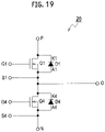
- Fig. 19 illustrates a schematic circuit representative of a 2-in-1 module, which is the power module 20 according to the embodiment.
- two MOSFETs Q1, Q4 are included in one module.
- Reference numeral G1 denotes a gate signal terminal of the MOSFET Q1
- reference numeral S1 denotes a source sense terminal of the MOSFET Q1.
- Reference numeral G4 denotes a gate signal terminal of the MOSFET Q4
- reference numeral S4 denotes a source sense terminal of the MOSFET Q4.
- Reference numeral P denotes a positive side power input terminal
- reference numeral N denotes a negative side power input terminal
- reference numeral O denotes an output terminal.
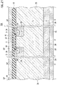
- a schematic cross-sectional structure of the SiC MOSFET as an example of the semiconductor device 100 (Q) applied to the power module 20 includes: a semiconductor substrate 26 composed of an n - type high resistivity layer; a p type base region 28 formed on the surface side of the semiconductor substrate 26; source regions 30 formed on the surface of the p type base regions 28; a gate insulating film 32 disposed on the surface of the semiconductor substrate 26 between the p type base regions 28; a gate electrode 38 disposed on the gate insulating film 32; a source electrode 34 connected to the source region 30 and the p type base region 28; an n + drain region 24 disposed on a back side surface opposite to the surface of the semiconductor substrate 26; and a drain pad electrode 36 connected to the n + drain region 24.
- the semiconductor device 100 is composed of a planar-gate-type n channel vertical SiC-MOSFET, the semiconductor device 100 may be composed of a trench-gate-type n channel vertical SiC-MOSFET, etc.
- GaN based FET etc. instead of SiC MOSFET are also applicable to the semiconductor device 100 (Q) applied to the power module 20 according to the embodiment.
- any one of an SiC based power device, a GaN based power device, and an AlN based power device is applicable to the semiconductor device 100 applied to the power module 20 according to the embodiment.
- a semiconductor of which the bandgap energy is from 1.1 eV to 8 eV, for example, can be used for the semiconductor device 100 applied to the power module 20 according to the embodiment.
- Fig. 21 illustrates a schematic cross-sectional structure of an SiC MOSFET including a source pad electrode SP and a gate pad electrode GP, which is an example of the semiconductor device 100 applied to the power module 20 according to the embodiment.
- the gate pad electrode GP is connected to the gate electrode 38 disposed on the gate insulating film 32, and the source pad electrode SP is connected to the source electrode 34 connected to the source region 30 and the p type base region 28.
- the gate pad electrode GP and the source pad electrode SP are disposed on an interlayer insulating film 44 for passivation which covers the surface of the semiconductor device 100.
- Microstructural transistor structure may be formed in the semiconductor substrate 26 below the gate pad electrode GP and the source pad electrode in the same manner as the center portion shown in Fig. 20 or 21 .
- the source pad electrode SP may be disposed to be extended onto the interlayer insulating film 44 for passivation, also in the transistor structure of the center portion.
- Fig. 22 illustrates a circuit configuration to connect the snubber capacitor C between the power terminal PL and the earth terminal (ground terminal) NL.
- large surge voltage Ldi/dt is produced by an inductance L included in a connection line due to a high switching speed of the SiC device.
- the surge voltage Ldi/dt changes dependent on a value of the inductance L
- the surge voltage Ldi/dt is superimposed on the power source V.
- Such a surge voltage Ldi/dt can be absorbed by the snubber capacitor C connected between the power terminal PL and the earth terminal (ground terminal) NL.
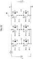
- the three-phase AC inverter 40 includes: a gate drive unit 50; a power module unit 52 connected to the gate drive unit 50 and a three-phase AC motor unit 54.
- U-phase, V-phase, and W-phase inverters are respectively connected to the three-phase AC motor unit 54 so as to correspond to U phase, V phase, and W phase of the three-phase AC motor unit 54, in the power module unit 52.
- the gate drive unit 50 is connected to the SiC MOSFETs Q1, Q4 as shown in Fig. 23
- the gate drive unit 50 is similarly connected also to the SiC MOSFETs Q2, Q5 and the SiC MOSFETs Q3, Q6 (not shown in Fig. 23 ).
- the SiC MOSFETs Q1, Q4, and Q2, Q5, and Q3, Q6 having inverter configurations are connected between a positive terminal (+) and a negative terminal (-) to which the converter 48 in a storage battery (E) 46 is connected. Furthermore, diodes D1-D6 are connected inversely in parallel to one another between the source and the drain of the SiC-MOSFETs Q1 to Q6.
- the three-phase power module unit 52 can also be formed also by similarly forming V phase and W phase inverters.
- the power module according to the embodiment can be formed as any one of 1-in-1, 2-in-1, 4-in-1, or 6-in-1 module.
- the power module with improved reliability so that the insulating layer and the metal layer may be hardly deviated from each other even if external force is applied thereon; and the fabrication method for such a power module.
- the insulating layer 7 is formed also between the leadframes 1 and 5 in Fig. 5 , the insulating layer 7 may not always be formed between the leadframes 1, 5, but may be formed only on a bottom surface of the leadframes 1, 5.
- the power module according to the present invention can be used for semiconductor modules, e.g. IGBT modules, diode modules, MOS modules (Si, SiC, GaN), etc.
- the power module according to the embodiment can also be used for structures which do not use insulating substrates, e.g. Direct Copper Bond (DBC) in case type modules.
- DBC Direct Copper Bond
Description
- The present invention described herein relates to a power module and a fabrication method for such a power module.
- Conventionally, there have been known power modules in which a power chip including a semiconductor device such as Insulated Gate Bipolar Transistor (IGBT) is mounted on a leadframe therein, and of which the whole system thereof is molded with resin (Refer to
Patent Literatures -
- Patent Literature 1:
Japanese Patent No. 3201277 - Patent Literature 2:
Japanese Patent Application Laying-Open Publication No. 2005-109100 - Document
JP 2001 118961 A - In conventional power modules, an insulating layer and a leadframe (metal layer) are contacted with each other on a flat surface. If external force is applied thereon in such a state where the insulating layer and the metal layer are contacted with each other on the flat surface, the insulating layer and the metal layer may be deviated (displaced) from each other, thereby causing insulation failure. Moreover, if the insulating layer and the metal layer are deviated from each other and thereby a gap is formed therebetween, a thermal resistance of the module may be increased. Thereby, since it becomes impossible to cool the semiconductor device as designed, there will be generated thermal run away of the semiconductor device, thermal deterioration of bonding layers, e.g. a solder layer, and fusing of bonding wires.
- The object of the present invention is to provide a power module with improved reliability so that an insulating layer and a metal layer may be hardly deviated from each other even if external force is applied thereon; and a fabrication method for such a power module.
- According to one aspect of the present invention, there is provided a power module according to
claim 1, comprising: an insulating layer; a metal layer disposed on the insulating layer; a semiconductor chip disposed on the metal layer; and a mold resin formed so as to cover the semiconductor chip and at least a part of the metal layer, wherein a groove into which a part of the insulating layer is inserted is formed on a surface of the metal layer facing the insulating layer. - According to another aspect of the present invention, there is provided a fabrication method for a power module according to claim 19, comprising: forming a groove on a bottom surface of a leadframe; bonding a semiconductor chip to the leadframe with a conductive bonding material; electrically connecting the semiconductor chip and the leadframe to each other using a connecting member; disposing the leadframe on a metallic mold and then forming an insulating layer on a bottom surface of the leadframe, the insulating layer formed so as to be inserted into the bottom surface of the leadframe; and after curing the insulating layer, closing the metallic mold, and then pouring a mold resin therein in order to mold the leadframe, the conductive bonding material, the semiconductor chip, and the connecting member.
- According to the present invention, there can be provided a power module with improved reliability so that the insulating layer and the metal layer may be hardly deviated from each other even if external force is applied thereon; and a fabrication method for such a power module.
-
- [
Fig. 1 ] A schematic cross-sectional structure diagram of a power module according to a comparative example. - [
Fig. 2 ] A schematic cross-sectional structure diagram of another power module according to the comparative example. - [
Fig. 3 ] A schematic cross-sectional structure diagram showing a usage example of the power module shown inFig. 1 . - [
Fig. 4 ] A schematic cross-sectional structure diagram showing a usage example of the power module shown inFig. 2 . - [
Fig. 5 ] A schematic cross-sectional structure diagram of a power module according to an example not covered by the claims. - [
Fig. 6 ] A schematic planar structure Fig. showing a usage example of the power module according to an example not covered by the claims. - [
Fig. 7 ] A schematic cross-sectional structure diagram taken in the line I-I ofFig. 5 . - [
Fig. 8 ] Another schematic cross-sectional structure diagram taken in the line I-I ofFig. 5 . - [
Fig. 9 ] Still another schematic cross-sectional structure diagram taken in the line I-I ofFig. 5 . - [
Fig. 10 ] An enlarged schematic cross-sectional structure diagram of a part of leadframe in the power module according to the embodiment. - [
Fig. 11 ] Another enlarged schematic cross-sectional structure diagram of the part of the leadframe in the power module according to the embodiment. - [
Fig. 12 ] Still another enlarged schematic cross-sectional structure diagram of the part of the leadframe in the power module according to the embodiment. - [
Fig. 13 ] Yet another enlarged schematic cross-sectional structure diagram of the part of the leadframe in the power module according to the embodiment. - [
Fig. 14 ] Yet another enlarged schematic cross-sectional structure diagram of the part of the leadframe in the power module according to the embodiment. - [
Fig. 15 ] (a) A cross-sectional diagram showing a state before forming a groove, (b) a cross-sectional diagram showing a state after forming the groove, (c) a cross-sectional diagram showing a state where a semiconductor chip is bonded thereon, (d) a cross-sectional diagram showing a state where an aluminum wire is connected thereto, (e) a cross-sectional diagram showing a state where an insulating layer is formed thereon, and (f) a cross-sectional diagram showing a state where the power module is molded, in process charts showing the fabrication method of the power module according to an example not covered by the claims. - [
Fig. 16 ] (a) cross-sectional diagram showing a state before forming a groove, (b) a cross-sectional diagram showing a state after forming the groove, (c) a cross-sectional diagram showing a state where a semiconductor chip is bonded thereon, (d) a cross-sectional diagram showing a state where an aluminum wire is connected thereto, (e) a cross-sectional diagram showing a state where the power module is molded, and (f) a cross-sectional diagram showing a state where an insulating layer is formed thereon, in process charts showing another fabrication method of the power module according to the embodiment. - [
Fig. 17 ] A schematic circuit representative diagram showing a 1-in-1 module, which is the power module according to the embodiment. - [
Fig. 18 ] A detail circuit representative diagram showing the 1-in-1 module, which is the power module according to the embodiment. - [
Fig. 19 ] A schematic circuit representative diagram showing a 2-in-1 module, which is the power module according to the embodiment. - [
Fig. 20 ] A schematic cross-sectional structure diagram showing an SiC MOSFET, which is an example of a semiconductor device applied to the power module according to the embodiment. - [
Fig. 21 ] A schematic cross-sectional structure diagram showing an SiC MOSFET including a source pad electrode SP and a gate pad electrode GP, which is an example of the semiconductor device applied to the power module according to the embodiment. - [
Fig. 22 ] An example of a circuit configuration in which a snubber capacitor is connected between a power terminal PL and an earth terminal (ground terminal) NL, in a schematic circuit configuration of a three-phase alternating current (AC) inverter composed using the power module according to the embodiment. - [
Fig. 23 ] A schematic circuit configuration diagram of the three-phase AC inverter composed using the power module according to the embodiment. - Next, a certain embodiment of the present invention will be described with reference to drawings. In the description of the following drawings, the identical or similar reference numeral is attached to the identical or similar part. However, it should be noted that the drawings are schematic and the relation between thickness and the plane size of each component part differs from an actual thing. Therefore, detailed thickness and size should be determined in consideration of the following explanation.
- Moreover, the embodiment described hereinafter merely exemplifies the device and method for materializing the technical idea of the present invention; and the embodiment of the present invention does not specify the material, shape, structure, placement, etc. of each component part as the following.
- A schematic cross-sectional structure of a
power module 20a according to a comparative example is illustrated as shown inFig. 1 . As shown inFig. 1 , firstly, asemiconductor chip 3 is bonded with asolder 2 on aleadframe 1. Subsequently, thesemiconductor chip 3 and aleadframe 5 are electrically connected to each other with analuminum wire 4. Subsequently, theleadframe 1 and theleadframe 5 are disposed on a metallic mold (not shown), and aninsulating layer 7 is formed on a surface of theleadframes 1 and 5 (hereafter referred to as a "bottom surface") opposite to a surface on which thesemiconductor chip 3 is mounted. Subsequently, the metallic mold is closed and then amold resin 6 is poured therein, and thereby thepower module 20a molded with themold resin 6 can be formed. - A schematic cross-sectional structure of
another power module 20b according to the comparative example is illustrated as shown inFig. 2 . As shown inFig. 2 , there may be adopted a structure of bonding ametallic plate 8 on a bottom surface of theinsulating layer 7. Thus, by disposing themetallic plate 8 on the outermost layer, theinsulating layer 7 is covered with themetallic plate 8, and thereby it can prevent from an externally caused crack. The configuration of other portions is the same as that of thepower module 20a. - A schematic cross-sectional structure showing a usage example of the
power module 20a shown inFig. 1 is illustrated as shown inFig. 3 , and a schematic cross-sectional structure showing a usage example of thepower module 20b shown inFig. 2 is illustrated as shown inFig. 4 . As shown inFigs. 3 and 4 , thepower modules heat sink 10 via a liquidthermal compound 9. - In this case, in the
power modules layer 7 and the leadframes (metal layers) 1, 5 are contacted with each other on a flat surface. If external force is applied thereon in such a state where the insulatinglayer 7 and themetal layers layer 7 and themetal layers layer 7 and themetal layers solder 2, and fusing of thealuminum wire 4. - Since the
thermal compound 9 is liquid, time and effort are required in work for coating. Moreover, thethermal compound 9 is also hardly treated since it is necessary to be coated uniformly and thinly. Furthermore, the whole of the power module (20a, 20b) becomes deformed by warping and restoring in a repetition of cooling and heating due to operating environments, and thereby the liquidthermal compound 9 may be gradually pushed out (pumped out) therefrom. If thethermal compound 9 is pumped out therefrom, a gap may be generated between a bottom surface of the power module (20a, 20b) and theheat sink 10, and thereby a thermal resistance of the portion where the gap is generated will be increased. As a result, since the semiconductor device cannot fully be cooled, it becomes a cause of the thermal run away of the semiconductor device, the thermal deterioration of bonding layers, e.g. asolder 2, and the fusing of thealuminum wire 4 as previously explained. - As shown in
Fig. 5 , apower module 20 according to an example not covered by the claims includes: an insulatinglayer 7; leadframes (metal layers) 1, 5 respectively disposed on the insulatinglayer 7; and asemiconductor chip 3 disposed on theleadframe 1, wherein agroove 11 into which a part of the insulatinglayer 7 is inserted is formed on a surface of theleadframes layer 7. - In the embodiment, the
groove 11 may also be formed outside a region to which a heat generated from thesemiconductor chip 3 is conducted. - Moreover, an angle between the
semiconductor chip 3 and thegroove 11 may be equal to or less than 45 degrees. - Moreover, the
groove 11 may be formed only outside the region to which the heat generated from thesemiconductor chip 3 is conducted. - Moreover, a cross-sectional shape of the
groove 11 may be at least one shape selected from the group consist of a rectangle shape, a semicircle shape, a semi-ellipse shape, triangular shape, and a wedge shape. - Moreover, the
groove 11 may be formed along in one direction or may be formed in a lattice-like shape. - Moreover, a surface roughening process may be applied on a surface of the
leadframes layer 7. - Moreover, the insulating
layer 7 may be formed of a material(s) softer than theleadframes - Moreover, a hardness of the insulating
layer 7 may be softer than A40 in durometer hardness. - Moreover, the insulating
layer 7 may be formed of an organic material(s). - Moreover, the insulating
layer 7 may be formed of a silicone based resin(s). - Moreover, the insulating
layer 7 may be filled up with a high thermally-conductive filler. - Moreover, the filler may be at least one selected from the group consist of aluminium oxide, silicon oxide, aluminum nitride, silicon nitride, boron nitride, beryllia, and magnesia.
- Moreover, the insulating
layer 7 may be formed before thesemiconductor chip 3 is molded with amold resin 6. - Moreover, an edge part of the insulating
layer 7 may be intervened between themold resin 6 and theleadframes - Moreover, the insulating
layer 7 may be formed after thesemiconductor chip 3 is molded with themold resin 6. - Moreover, the
mold resin 6 and theleadframes - Hereinafter, there will now be explained a configuration of the
power module 20 according to the embodiment in more detail, with reference toFig. 5 . As already explained, thegroove 11 into which a part of the insulatinglayer 7 is inserted is formed in the surface of theleadframes layer 7, in thepower module 20 according to the example. - A flexible resin (organic material) is used for the insulating
layer 7. The flexible resin is preferably a material(s) softer than theleadframes layer 7 is filled up with a high thermally-conductive filler of approximately 1 to 20 W/mK degrees, for example. As such a filler, aluminium oxide, silicon oxide, aluminum nitride, silicon nitride, boron nitride, beryllia, magnesia, etc. can be used. - Thus, since the insulating
layer 7 is tightly insert in thegroove 11 by using the flexible resin for the insulatinglayer 7, the insulatinglayer 7 can be strongly bonded to theleadframes layer 7 is sufficiently compatible with the surface of theheat sink 10 due to the flexibility thereof, it becomes unnecessary to coat the liquidthermal compound 9 between the bottom surface of thepower module 20 and theheat sink 10 as in the case of the comparative example. - As shown in the principal part B in
Fig. 5 , thegroove 11 is formed outside a region extended in downward direction by only the angle C from a bottom head of thesolder 2. Since a heat generated from thesemiconductor chip 3 is conducted by being spread at approximately 45 degrees, it is preferable to set the angle C to be equal to or less than 45 degrees. Accordingly, since nogroove 11 is formed in a region to which the heat is conducted, a defect due to increase of the thermal resistance can be avoided, thereby improving the reliability thereof. - A schematic planar structure showing a usage example of the
power module 20 according to the example is illustrated as shown inFig. 6 . As shown inFig. 6 , theleadframes heat sink 10 withscrews layer 7, thepower module 20 is strongly joined to theheat sink 10. - A schematic cross-sectional structure taken in the line I-I shown in
Fig. 5 is illustrated as shown inFig. 7 . As shown inFig. 7 , a plurality of thegrooves 11 may be formed in a vertical direction. The vertical direction used herein is a short-side direction of thepower module 20. In this case, a bonding strength between the insulatinglayer 7 and themetal layers power module 20. - Another schematic cross-sectional structure taken in the line I-I shown in
Fig. 5 is illustrated as shown inFig. 8 . As shown inFig. 8 , a plurality of thegrooves 11 may be formed in a horizontal direction. The horizontal direction used herein is a long-side direction of thepower module 20. In this case, a bonding strength between the insulatinglayer 7 and themetal layers power module 20. - Still another schematic cross-sectional structure taken in the line I-I shown in
Fig. 5 is illustrated as shown inFig. 9 . Thegroove 11 may be formed in a lattice-like shape as shown inFig. 9 . Thereby, the bonding strength between the insulatinglayer 7 and themetal layers groove 11 formed in one direction, e.g. the vertical direction or horizontal direction. - Although the case where the
groove 11 is formed in a vertical or direction, or in a lattice-like shape has been exemplified herein, the formed direction of thegroove 11 is not limited to the above-mentioned examples. For example, thegroove 11 may be obliquely formed in one direction with respect to thesemiconductor chip 3, or may be obliquely formed in a lattice-like shape. - An enlarged schematic cross-sectional structure showing a part of the
leadframe 5 in thepower module 20 according to the example is illustrated as shown inFig. 10 . As shown inFig. 10 , thegroove 12 may be formed in a rectangle shape in a cross sectional view. If the thickness of theleadframe 5 is approximately 3 mm, for example, the depth of thegroove 12 is preferably approximately 0.5 to 1.5 mm, for example. Moreover, the distance between theadjacent grooves 12, and the width of eachgroove 12 are preferable to be approximately equal to each other. - Another enlarged schematic cross-sectional structure showing a part of the
leadframe 5 in thepower module 20 according to the example is illustrated as shown inFig. 11 . As shown inFig. 11 , thegroove 13 may be formed in a semicircle shape or semi-ellipse shape in a cross sectional view. The depth and the distance of such agroove 13 are also the same as those of the case of therectangular groove 12. - Yet another enlarged schematic cross-sectional structure showing a part of the
leadframe 5 in thepower module 20 according to the example is illustrated as shown inFig. 12 . As shown inFig. 12 , thegroove 14 may be formed in a triangular shape in a cross sectional view. The depth and the distance of such agroove 14 are also the same as those of the case of therectangular groove 12. - Yet another enlarged schematic cross-sectional structure showing a part of the
leadframe 5 in thepower module 20 according to the example is illustrated as shown inFig. 13 . As shown inFig. 13 , thegroove 15 may be formed in a wedge shape in a cross sectional view. The depth and the distance of such agroove 15 are also the same as those of the case of therectangular groove 12. - Yet another enlarged schematic cross-sectional structure showing a part of the
leadframe 5 in thepower module 20 according to the example is illustrated as shown inFig. 14 . As shown inFig. 14 , thegroove 16 may be formed by applying a surface roughening process to the bottom surface of theleadframes layer 7 and themetal layers - In the embodiment, although there have been exemplified the case where the respective grooves 12-15 are formed in a rectangle shape, a semicircle shape, a semi-ellipse shape, a triangular shape, and a wedge shape, and the case where the
groove 16 is formed by applying the surface roughening process, these cases may be combined with one another. Although not specifically mentioned in the example, the grooves 12-16 are, of course, formed outside a region extended in downward direction by only the angle C from the bottom head of thesolder 2, as shown in the principal part B inFig. 5 . - A process showing a fabrication method of the
power module 20 according to the example is illustrated as shown inFig. 15 . Although only a portion at the side of theleadframe 1 is shown inFig. 15 , other portions are as being shown inFig. 5 . - Firstly, the
groove 11 is formed in the bottom surface of theleadframes Figs. 15(a) and 15(b) . The fabrication method of thegroove 11 is not particularly limited thereto. For example, when punching theleadframes groove 11 may be simultaneously formed. - Next, as shown in
Fig. 15(c) , thesemiconductor chip 3 is bonded to theleadframe 1 with thesolder 2. A high thermally-conductive silver paste may be used as thesolder layer 2. - Next, as shown in
Fig. 15(D) , in order to electrically connect thesemiconductor chip 3 and theleadframe 5 to each other, ultrasonic bonding is applied thereto using thealuminum wire 4. In this case, theleadframe 1 and theleadframe 5 are connected to each other with a connector bar (not shown) in order to prevent from relative positions thereof being displaced from each other at the time of the ultrasonic bonding. The connector bar will be removed after the ultrasonic bonding is completed. - Next, as shown in
Fig. 15(e) , theleadframe 1 and theleadframe 5 are disposed on a metallic mold (not shown), and then the insulatinglayer 7 is formed on the bottom surfaces of theleadframes layer 7 is approximately 0.5 mm. Screen printing etc. may be suitable as a fabrication method of the insulatinglayer 7. At this time, the insulatinglayer 7 is formed so as to cover a corner portion P of theleadframes - Finally, after curing the insulating
layer 7, the metallic mold is closed, and then themold resin 6 is poured therein in order to mold theleadframe 1, thesolder 2, thesemiconductor chip 3, thealuminum wire 4, and theleadframe 5, as shown inFig. 15(f) . Thereby, thepower module 20 molded with themold resin 6 can be fabricated. - According to such a fabrication method, an edge part of the insulating
layer 7 is intervened between themold resin 6 and theleadframes leadframes - A process showing another fabrication method of the
power module 20 according to the embodiment is illustrated as shown inFig. 16 . A different point from the fabrication method 1 (Fig. 15 ) is a point that the order of the process of molding and the process of forming the insulatinglayer 7 are reversed. - The respective processes of
Figs. 16(a) to 16(d) are the same as the respective processes ofFigs. 15(a) and 15(b) . More specifically, thegroove 11 is formed in the bottom surfaces of theleadframes semiconductor chip 3 is bonded to theleadframe 1, and then thesemiconductor chip 3 and theleadframe 5 are connected to each other with thealuminum wire 4. In this step, as shown inFig. 16(e) , the metallic mold is closed and then themold resin 6 is poured therein. Themold resin 6 and theleadframe 1 are formed so as to be flush with each other at the corner portion P, at this time. Finally, as shown inFig. 16(f) , the insulatinglayer 7 is formed on the surface of themold resin 6 and the surface of theleadframes leadframes layer 7, and thereby a possibility of short-circuiting at the corner portion P can also be reduced. - As mentioned above, the
power module 20 according to the embodiment is a resin-sealed semiconductor module having a vertical structure of the semiconductor chip / the metal layer / the insulating layer. In such a structure, thegroove 11 into which a part of the insulatinglayer 7 is inserted is formed in the surface of themetal layers layer 7. Thereby, even if external force is applied thereon, since the bonding strength between the insulatinglayer 7 and themetal layers layer 7 and themetal layers layer 7 and themetal layers solder 2, and fusing of thealuminum wire 4, thereby improving the reliability thereof. Moreover, since thegroove 11 is arranged in consideration of spreading of heat so that conduction of the heat generated from thesemiconductor chip 3 may be hardly obstructed by thegroove 11, the cooling capability is not inhibited. In addition, since the flexible resin is used for the insulatinglayer 7, the liquidthermal compound 9 becomes unnecessary, and therefore it becomes possible to provide thepower module 20 easy to handle. - Hereinafter, there will now be explained examples of the
power module 20 according to the embodiment. Needless to say, thegroove 11 can be formed also in theleadframes power module 20 explained below. A formed direction, a cross-sectional shape, and other details configuration of thegroove 11 are the same as described above. -
Fig. 11 illustrates a schematic circuit representative of a one-in-one (1-in-1) module, which is thepower module 20 according to the embodiment. Moreover,Fig. 18 illustrates a detail circuit representative of the 1-in-1 module, which is thepower module 20 according to the embodiment. - The
power module 20 according to the embodiment has a configuration of 1-in-1 module. More specifically, one MOSFETQ is included in one module. As an example, five chips (MOS transistor × 5) can be mounted thereon, and a maximum of five pieces of the MOSFETs respectively can be connected to one another in parallel. Note that it is also possible to mount a part of five pieces of the chips for the diode DI thereon. - The diode DI connected to the MOSFETQ inversely in parallel is shown in
Fig. 17 . A main electrode of the MOSFETQ is expressed with a drain terminal DT and a source terminal ST. - More particularly, as shown in
Fig. 18 , a sense MOSFET Qs is connected to the MOSFETQ in parallel. The sense MOSFET Qs is formed as a minuteness transistor in the same chip as the MOSFET Q. InFig. 18 , reference numeral SS denotes a source sense terminal, reference numeral CS denotes a current sense terminal, and reference numeral G denotes a gate signal terminal. Note that, also in the semiconductor device Q according to the embodiment, the sense MOSFET Qs is formed as a minuteness transistor in the same chip. - Moreover,
Fig. 19 illustrates a schematic circuit representative of a 2-in-1 module, which is thepower module 20 according to the embodiment. As shown inFig. 19 , two MOSFETs Q1, Q4 are included in one module. Reference numeral G1 denotes a gate signal terminal of the MOSFET Q1, and reference numeral S1 denotes a source sense terminal of the MOSFET Q1. Reference numeral G4 denotes a gate signal terminal of the MOSFET Q4, and reference numeral S4 denotes a source sense terminal of the MOSFET Q4. Reference numeral P denotes a positive side power input terminal, reference numeral N denotes a negative side power input terminal, and reference numeral O denotes an output terminal. - As shown in
Fig. 20 , a schematic cross-sectional structure of the SiC MOSFET as an example of the semiconductor device 100 (Q) applied to thepower module 20 according to the embodiment includes: asemiconductor substrate 26 composed of an n- type high resistivity layer; a ptype base region 28 formed on the surface side of thesemiconductor substrate 26;source regions 30 formed on the surface of the ptype base regions 28; agate insulating film 32 disposed on the surface of thesemiconductor substrate 26 between the ptype base regions 28; agate electrode 38 disposed on thegate insulating film 32; asource electrode 34 connected to thesource region 30 and the ptype base region 28; an n+ drain region 24 disposed on a back side surface opposite to the surface of thesemiconductor substrate 26; and adrain pad electrode 36 connected to the n+ drain region 24. - In
Fig. 20 , although thesemiconductor device 100 is composed of a planar-gate-type n channel vertical SiC-MOSFET, thesemiconductor device 100 may be composed of a trench-gate-type n channel vertical SiC-MOSFET, etc. - Moreover, a GaN based FET etc. instead of SiC MOSFET are also applicable to the semiconductor device 100 (Q) applied to the
power module 20 according to the embodiment. - Any one of an SiC based power device, a GaN based power device, and an AlN based power device is applicable to the
semiconductor device 100 applied to thepower module 20 according to the embodiment. - Furthermore, a semiconductor of which the bandgap energy is from 1.1 eV to 8 eV, for example, can be used for the
semiconductor device 100 applied to thepower module 20 according to the embodiment. -
Fig. 21 illustrates a schematic cross-sectional structure of an SiC MOSFET including a source pad electrode SP and a gate pad electrode GP, which is an example of thesemiconductor device 100 applied to thepower module 20 according to the embodiment. The gate pad electrode GP is connected to thegate electrode 38 disposed on thegate insulating film 32, and the source pad electrode SP is connected to thesource electrode 34 connected to thesource region 30 and the ptype base region 28. - Moreover, as shown in
Fig. 21 , the gate pad electrode GP and the source pad electrode SP are disposed on aninterlayer insulating film 44 for passivation which covers the surface of thesemiconductor device 100. Microstructural transistor structure may be formed in thesemiconductor substrate 26 below the gate pad electrode GP and the source pad electrode in the same manner as the center portion shown inFig. 20 or21 . - Furthermore, as shown in
Fig. 21 , the source pad electrode SP may be disposed to be extended onto theinterlayer insulating film 44 for passivation, also in the transistor structure of the center portion. - In the
power module 20 according to the embodiment,Fig. 22 illustrates a circuit configuration to connect the snubber capacitor C between the power terminal PL and the earth terminal (ground terminal) NL. When connecting thepower module 20 according to the embodiment to the power source E, large surge voltage Ldi/dt is produced by an inductance L included in a connection line due to a high switching speed of the SiC device. For example, the surge voltage Ldi/dt is expressed as follows: Ldi/dt = 3×10⁹ (A/s), where a current change di=300A, and a time variation accompanying switching dt = 100 ns. Although a value of the surge voltage Ldi/dt changes dependent on a value of the inductance L, the surge voltage Ldi/dt is superimposed on the power source V. Such a surge voltage Ldi/dt can be absorbed by the snubber capacitor C connected between the power terminal PL and the earth terminal (ground terminal) NL. - Next, there will now be explained a three-
phase AC inverter 40 composed by using thepower module 20 according to the embodiment with reference toFig. 23 . - As shown in
Fig. 23 , the three-phase AC inverter 40 includes: agate drive unit 50; apower module unit 52 connected to thegate drive unit 50 and a three-phase AC motor unit 54.U-phase, V-phase, and W-phase inverters are respectively connected to the three-phaseAC motor unit 54 so as to correspond to U phase, V phase, and W phase of the three-phaseAC motor unit 54, in thepower module unit 52. In this case, although thegate drive unit 50 is connected to the SiC MOSFETs Q1, Q4 as shown inFig. 23 , thegate drive unit 50 is similarly connected also to the SiC MOSFETs Q2, Q5 and the SiC MOSFETs Q3, Q6 (not shown inFig. 23 ). - In the
power module unit 52, the SiC MOSFETs Q1, Q4, and Q2, Q5, and Q3, Q6 having inverter configurations are connected between a positive terminal (+) and a negative terminal (-) to which theconverter 48 in a storage battery (E) 46 is connected. Furthermore, diodes D1-D6 are connected inversely in parallel to one another between the source and the drain of the SiC-MOSFETs Q1 to Q6. - Although the structure of the single phase inverter corresponding to U phase portion of
Fig. 23 has been explained in thepower module 20 according to the embodiment, the three-phasepower module unit 52 can also be formed also by similarly forming V phase and W phase inverters. - The power module according to the embodiment can be formed as any one of 1-in-1, 2-in-1, 4-in-1, or 6-in-1 module.
- As explained above, according to the present invention, there can be provided the power module with improved reliability so that the insulating layer and the metal layer may be hardly deviated from each other even if external force is applied thereon; and the fabrication method for such a power module.
- As explained above, the embodiment of the present invention has been described, as a disclosure including associated description and drawings to be construed as illustrative, not restrictive. Although the insulating
layer 7 is formed also between theleadframes Fig. 5 , the insulatinglayer 7 may not always be formed between theleadframes leadframes - The power module according to the present invention can be used for semiconductor modules, e.g. IGBT modules, diode modules, MOS modules (Si, SiC, GaN), etc. The power module according to the embodiment can also be used for structures which do not use insulating substrates, e.g. Direct Copper Bond (DBC) in case type modules.
-
- 1, 5: Metal layer (leadframe)
- 3: Semiconductor chip
- 6: Mold resin
- 7: Insulating layer
- 11-16: groove
- 20: power module
Claims (20)
- A power module (20) comprising:an insulating layer (7) having a top surface and a bottom surface;a metal layer (1) disposed on the top surface of the insulating layer (7);a semiconductor chip (3) disposed on the metal layer (1); anda mold resin (6) formed so as to cover the semiconductor chip (3) and at least a part of the metal layer (1), and only the top surface side of the insulation layer (7), whereina groove (11) into which a part of the insulating layer (7) is inserted is formed on a surface of the metal layer (1) facing the insulating layer (7), and the bottom surface side of the insulation layer (7) is a flat surface.
- The power module according to claim 1, wherein
a plurality of the grooves (11) are formed outside a region_of the metal layer (1) opposite to the semiconductor chip (3). - The power module according to claim 2, wherein
the region is a region where an angle (C) between a line and a flat surface of the metal layer (1) is equal to or less than 45 degrees, the line connecting between an edge part of the semiconductor chip (3) and an edge part of the groove (11) nearest to the semiconductor chip (3) among the plurality of the grooves. - The power module according to claim 2 or 3, wherein
the plurality of the grooves (11) are formed only outside a region of the metal layer (1) opposite to the semiconductor chip (3). - The power module according to any one of claims 1-4, wherein:a cross-sectional shape of the groove (11) is at least one shape selected from the group consist of a rectangle shape, a semicircle shape, a semi-ellipse shape, triangular shape, and a wedge shape; anda depth of the groove (11) is approximately 0.5 to 1.5 mm and a thickness of the metal layer (1) is approximately 3.0 mm.
- The power module according to any one of claims 1-5, wherein
the groove is formed along in one direction or is formed in a lattice-like shape. - The power module according to any one of claims 1-6, wherein
a surface roughening process is applied on a surface of the metal layer (5) facing the insulating layer (7). - The power module according to any one of claims 1-7, wherein
the insulating layer (7) is formed of a material softer than the metal layer (1). - The power module according to claim 8, wherein
a hardness of the insulating layer (7) is softer than A40 in durometer hardness. - The power module according to any one of claims 1-9, wherein
the insulating layer (7) is formed of an organic material. - The power module according to any one of claims 1-10, wherein
the insulating layer (7) is formed of a silicone based resin. - The power module according to any one of claims 1-11, wherein
the insulating layer (7) is filled up with a high thermally-conductive filler. - The power module according to claim 12, wherein
the filler is at least one selected from the group consist of aluminium oxide, silicon oxide, aluminum nitride, silicon nitride, boron nitride, beryllia, and magnesia. - The power module according to any one of claims 1-13, wherein
a surface of the mold resin (6) and a surface of the metal layer (1) are flush with each other at a corner portion of the metal layer, and the insulating layer (7) is formed on the surface of the mold resin (6) and the surface of the leadframe which are flush with each other. - The power module according to any one of claims 2-13, wherein
a distance between the adjacent grooves, and a width of each groove are approximately equal to each other. - The power module according to claim 15, whereinthe semiconductor chip (3) is formed of one selected from the group consist of an SiC based power device, a GaN based power device, and an AIN based power device; anda current change rate di/dt thereof is approximately 3×10⁹ (A/s).
- The power module according to claim 1, wherein
the groove is formed in a short-side direction of the power module or in a long-side direction of the power module. - The power module according to any one of claims 1-17, wherein
the power module (20) is formed as any one selected from the group consisting of a 1-in-1 module, a 2-in-1 module, a 4-in-1 module, and a 6-in-1 module. - A fabrication method for a power module (20) comprising:forming a groove (11) on a bottom surface of a leadframe (1);bonding a semiconductor chip (3) to the leadframe (1) with a conductive bonding material (2);electrically connecting the semiconductor chip (3) and the leadframe (1) to each other using a connecting member (4);disposing the leadframe (1) on a metallic mold and closing the metallic mold, and then pouring a mold resin (6) therein in order to mold the leadframe (1), the conductive bonding material (2), the semiconductor chip (3), and the connecting member (4); andforming an insulating layer (7) on a bottom surface of the leadframe (1), the insulating layer (7) formed so as to be inserted into the bottom surface of the leadframe (1), the insulating layer (7) having a top surface and a bottom surface, the bottom surface side of the insulation layer (7) formed to be a flat surface, so that the mold resin (6) covers only the top surface side of the insulation layer (7).
- The fabrication method for a power module according to claim 19, wherein
in the forming of the groove, the groove (11) is formed in a short-side direction of the power module (20) or in a long-side direction of the power module (20) .
Applications Claiming Priority (2)
| Application Number | Priority Date | Filing Date | Title |
|---|---|---|---|
| JP2013151685A JP2015023211A (en) | 2013-07-22 | 2013-07-22 | Power module and method for manufacturing the same |
| PCT/JP2014/068978 WO2015012180A1 (en) | 2013-07-22 | 2014-07-17 | Power module and manufacturing method thereof |
Publications (3)
| Publication Number | Publication Date |
|---|---|
| EP3026701A1 EP3026701A1 (en) | 2016-06-01 |
| EP3026701A4 EP3026701A4 (en) | 2017-03-08 |
| EP3026701B1 true EP3026701B1 (en) | 2022-11-16 |
Family
ID=52393222
Family Applications (1)
| Application Number | Title | Priority Date | Filing Date |
|---|---|---|---|
| EP14829390.5A Active EP3026701B1 (en) | 2013-07-22 | 2014-07-17 | Power module and manufacturing method thereof |
Country Status (4)
| Country | Link |
|---|---|
| US (1) | US9721875B2 (en) |
| EP (1) | EP3026701B1 (en) |
| JP (1) | JP2015023211A (en) |
| WO (1) | WO2015012180A1 (en) |
Families Citing this family (10)
| Publication number | Priority date | Publication date | Assignee | Title |
|---|---|---|---|---|
| JP6332439B2 (en) * | 2014-03-31 | 2018-05-30 | 富士電機株式会社 | Power converter |
| JP6841199B2 (en) * | 2017-09-29 | 2021-03-10 | 三菱電機株式会社 | Semiconductor device |
| US11317546B2 (en) | 2018-06-26 | 2022-04-26 | Ford Global Technologies, Llc | Vehicle power module assembly |
| CN112567504A (en) | 2018-11-30 | 2021-03-26 | 日立金属株式会社 | Electric connection member, electric connection structure, and method for manufacturing electric connection structure |
| JP6818801B2 (en) * | 2019-04-01 | 2021-01-20 | ローム株式会社 | Power module and its manufacturing method |
| EP3956924A1 (en) | 2019-04-18 | 2022-02-23 | Hitachi Energy Switzerland AG | Power semiconductor module with laser-welded leadframe |
| CN110416178A (en) * | 2019-07-12 | 2019-11-05 | 南通沃特光电科技有限公司 | A kind of integrated circuit package structure and its packaging method |
| US11145578B2 (en) | 2019-09-24 | 2021-10-12 | Infineon Technologies Ag | Semiconductor package with top or bottom side cooling and method for manufacturing the semiconductor package |
| US20230112582A1 (en) * | 2020-03-31 | 2023-04-13 | Hitachi Energy Switzerland Ag | Power Module Device with an Embedded Power Semiconductor Device |
| WO2024009458A1 (en) * | 2022-07-07 | 2024-01-11 | 三菱電機株式会社 | Semiconductor device and power converter |
Citations (1)
| Publication number | Priority date | Publication date | Assignee | Title |
|---|---|---|---|---|
| JP2001118961A (en) * | 1999-10-15 | 2001-04-27 | Mitsubishi Electric Corp | Resin-sealed power semicondcutor device and its manufacturing method |
Family Cites Families (17)
| Publication number | Priority date | Publication date | Assignee | Title |
|---|---|---|---|---|
| JP3201277B2 (en) | 1996-09-11 | 2001-08-20 | 株式会社日立製作所 | Semiconductor device |
| JPH10125826A (en) * | 1996-10-24 | 1998-05-15 | Hitachi Ltd | Semiconductor device and manufacture thereof |
| JP3605547B2 (en) * | 1999-06-11 | 2004-12-22 | 松下電器産業株式会社 | Heat dissipating substrate and manufacturing method thereof |
| JP2002167560A (en) * | 2000-12-01 | 2002-06-11 | Sekisui Chem Co Ltd | Thermally conductive resin sheet |
| JP2005109100A (en) | 2003-09-30 | 2005-04-21 | Mitsubishi Electric Corp | Semiconductor device and manufacturing method thereof |
| JP5186095B2 (en) * | 2006-10-02 | 2013-04-17 | 株式会社日立製作所 | Gate drive circuit |
| JP2008153430A (en) * | 2006-12-18 | 2008-07-03 | Mitsubishi Electric Corp | Heatsink substrate and heat conductive sheet, and power module using these |
| JP2008300379A (en) * | 2007-05-29 | 2008-12-11 | Sumitomo Electric Ind Ltd | Power module |
| JP5262983B2 (en) * | 2009-05-19 | 2013-08-14 | 株式会社デンソー | Mold package and manufacturing method thereof |
| JP2011100757A (en) * | 2009-11-04 | 2011-05-19 | Denki Kagaku Kogyo Kk | Electronic component, and method of manufacturing the same |
| JP5246143B2 (en) * | 2009-11-24 | 2013-07-24 | 富士電機株式会社 | SEMICONDUCTOR MODULE, ITS MANUFACTURING METHOD, AND ELECTRIC DEVICE |
| CN103125022B (en) * | 2010-07-01 | 2016-01-20 | 三菱电机株式会社 | Power semiconductor modular, power inverter and rolling stock |
| JP5409551B2 (en) * | 2010-08-24 | 2014-02-05 | 新電元工業株式会社 | Semiconductor device |
| JP5251991B2 (en) * | 2011-01-14 | 2013-07-31 | トヨタ自動車株式会社 | Semiconductor module |
| JP5249365B2 (en) * | 2011-01-26 | 2013-07-31 | 三菱電機株式会社 | Power converter |
| JP5690752B2 (en) * | 2012-01-10 | 2015-03-25 | 日立オートモティブシステムズ株式会社 | Power semiconductor module and method of manufacturing power semiconductor module |
| JP2013258387A (en) * | 2012-05-15 | 2013-12-26 | Rohm Co Ltd | Power-module semiconductor device |
-
2013
- 2013-07-22 JP JP2013151685A patent/JP2015023211A/en active Pending
-
2014
- 2014-07-17 EP EP14829390.5A patent/EP3026701B1/en active Active
- 2014-07-17 WO PCT/JP2014/068978 patent/WO2015012180A1/en active Application Filing
-
2016
- 2016-01-21 US US15/003,156 patent/US9721875B2/en active Active
Patent Citations (1)
| Publication number | Priority date | Publication date | Assignee | Title |
|---|---|---|---|---|
| JP2001118961A (en) * | 1999-10-15 | 2001-04-27 | Mitsubishi Electric Corp | Resin-sealed power semicondcutor device and its manufacturing method |
Also Published As
| Publication number | Publication date |
|---|---|
| EP3026701A1 (en) | 2016-06-01 |
| US20160141231A1 (en) | 2016-05-19 |
| EP3026701A4 (en) | 2017-03-08 |
| WO2015012180A1 (en) | 2015-01-29 |
| JP2015023211A (en) | 2015-02-02 |
| US9721875B2 (en) | 2017-08-01 |
Similar Documents
| Publication | Publication Date | Title |
|---|---|---|
| EP3026701B1 (en) | Power module and manufacturing method thereof | |
| JP6280265B2 (en) | Power module semiconductor device | |
| US10778113B2 (en) | Intelligent power module, electric vehicle, and hybrid car | |
| JP5067267B2 (en) | Resin-sealed semiconductor device and manufacturing method thereof | |
| JP6077773B2 (en) | Power module semiconductor device | |
| EP3026700B1 (en) | Power module and manufacturing method thereof | |
| US9437508B2 (en) | Method for manufacturing semiconductor device and semiconductor device | |
| US20180350710A1 (en) | Semiconductor device, and power module | |
| US20190295991A1 (en) | Semiconductor device having plate-shaped metal terminals facing one another | |
| US20150130042A1 (en) | Semiconductor module with radiation fins | |
| JPWO2018181417A1 (en) | Power module and method of manufacturing the same | |
| JP2012248700A (en) | Semiconductor device | |
| WO2018047485A1 (en) | Power module and inverter device | |
| JP6575739B1 (en) | Semiconductor device, semiconductor device manufacturing method, and power conversion device | |
| JP6660412B2 (en) | Semiconductor device | |
| JP6818801B2 (en) | Power module and its manufacturing method | |
| JP7019024B2 (en) | Semiconductor equipment and power conversion equipment | |
| JP6630762B2 (en) | Power module | |
| CN116438655A (en) | Power semiconductor module, method for manufacturing the same, and power conversion device | |
| JP2019040955A (en) | Method of manufacturing semiconductor module |
Legal Events
| Date | Code | Title | Description |
|---|---|---|---|
| PUAI | Public reference made under article 153(3) epc to a published international application that has entered the european phase |
Free format text: ORIGINAL CODE: 0009012 |
|
| STAA | Information on the status of an ep patent application or granted ep patent |
Free format text: STATUS: REQUEST FOR EXAMINATION WAS MADE |
|
| 17P | Request for examination filed |
Effective date: 20160222 |
|
| AK | Designated contracting states |
Kind code of ref document: A1 Designated state(s): AL AT BE BG CH CY CZ DE DK EE ES FI FR GB GR HR HU IE IS IT LI LT LU LV MC MK MT NL NO PL PT RO RS SE SI SK SM TR |
|
| AX | Request for extension of the european patent |
Extension state: BA ME |
|
| DAX | Request for extension of the european patent (deleted) | ||
| A4 | Supplementary search report drawn up and despatched |
Effective date: 20170202 |
|
| RIC1 | Information provided on ipc code assigned before grant |
Ipc: H01L 23/495 20060101AFI20170127BHEP Ipc: H01L 23/34 20060101ALI20170127BHEP |
|
| STAA | Information on the status of an ep patent application or granted ep patent |
Free format text: STATUS: EXAMINATION IS IN PROGRESS |
|
| 17Q | First examination report despatched |
Effective date: 20210429 |
|
| STAA | Information on the status of an ep patent application or granted ep patent |
Free format text: STATUS: EXAMINATION IS IN PROGRESS |
|
| REG | Reference to a national code |
Ref country code: DE Ref legal event code: R079 Ref document number: 602014085567 Country of ref document: DE Free format text: PREVIOUS MAIN CLASS: H01L0023340000 Ipc: H01L0023495000 |
|
| GRAP | Despatch of communication of intention to grant a patent |
Free format text: ORIGINAL CODE: EPIDOSNIGR1 |
|
| STAA | Information on the status of an ep patent application or granted ep patent |
Free format text: STATUS: GRANT OF PATENT IS INTENDED |
|
| RIC1 | Information provided on ipc code assigned before grant |
Ipc: H01L 23/31 20060101ALI20220428BHEP Ipc: H01L 23/34 20060101ALI20220428BHEP Ipc: H01L 23/495 20060101AFI20220428BHEP |
|
| INTG | Intention to grant announced |
Effective date: 20220601 |
|
| GRAS | Grant fee paid |
Free format text: ORIGINAL CODE: EPIDOSNIGR3 |
|
| GRAA | (expected) grant |
Free format text: ORIGINAL CODE: 0009210 |
|
| STAA | Information on the status of an ep patent application or granted ep patent |
Free format text: STATUS: THE PATENT HAS BEEN GRANTED |
|
| AK | Designated contracting states |
Kind code of ref document: B1 Designated state(s): AL AT BE BG CH CY CZ DE DK EE ES FI FR GB GR HR HU IE IS IT LI LT LU LV MC MK MT NL NO PL PT RO RS SE SI SK SM TR |
|
| REG | Reference to a national code |
Ref country code: GB Ref legal event code: FG4D |
|
| REG | Reference to a national code |
Ref country code: CH Ref legal event code: EP |
|
| REG | Reference to a national code |
Ref country code: DE Ref legal event code: R096 Ref document number: 602014085567 Country of ref document: DE |
|
| REG | Reference to a national code |
Ref country code: IE Ref legal event code: FG4D |
|
| REG | Reference to a national code |
Ref country code: AT Ref legal event code: REF Ref document number: 1532291 Country of ref document: AT Kind code of ref document: T Effective date: 20221215 |
|
| REG | Reference to a national code |
Ref country code: LT Ref legal event code: MG9D |
|
| REG | Reference to a national code |
Ref country code: NL Ref legal event code: MP Effective date: 20221116 |
|
| REG | Reference to a national code |
Ref country code: AT Ref legal event code: MK05 Ref document number: 1532291 Country of ref document: AT Kind code of ref document: T Effective date: 20221116 |
|
| PG25 | Lapsed in a contracting state [announced via postgrant information from national office to epo] |
Ref country code: SE Free format text: LAPSE BECAUSE OF FAILURE TO SUBMIT A TRANSLATION OF THE DESCRIPTION OR TO PAY THE FEE WITHIN THE PRESCRIBED TIME-LIMIT Effective date: 20221116 Ref country code: PT Free format text: LAPSE BECAUSE OF FAILURE TO SUBMIT A TRANSLATION OF THE DESCRIPTION OR TO PAY THE FEE WITHIN THE PRESCRIBED TIME-LIMIT Effective date: 20230316 Ref country code: NO Free format text: LAPSE BECAUSE OF FAILURE TO SUBMIT A TRANSLATION OF THE DESCRIPTION OR TO PAY THE FEE WITHIN THE PRESCRIBED TIME-LIMIT Effective date: 20230216 Ref country code: LT Free format text: LAPSE BECAUSE OF FAILURE TO SUBMIT A TRANSLATION OF THE DESCRIPTION OR TO PAY THE FEE WITHIN THE PRESCRIBED TIME-LIMIT Effective date: 20221116 Ref country code: FI Free format text: LAPSE BECAUSE OF FAILURE TO SUBMIT A TRANSLATION OF THE DESCRIPTION OR TO PAY THE FEE WITHIN THE PRESCRIBED TIME-LIMIT Effective date: 20221116 Ref country code: ES Free format text: LAPSE BECAUSE OF FAILURE TO SUBMIT A TRANSLATION OF THE DESCRIPTION OR TO PAY THE FEE WITHIN THE PRESCRIBED TIME-LIMIT Effective date: 20221116 Ref country code: AT Free format text: LAPSE BECAUSE OF FAILURE TO SUBMIT A TRANSLATION OF THE DESCRIPTION OR TO PAY THE FEE WITHIN THE PRESCRIBED TIME-LIMIT Effective date: 20221116 |
|
| PG25 | Lapsed in a contracting state [announced via postgrant information from national office to epo] |
Ref country code: RS Free format text: LAPSE BECAUSE OF FAILURE TO SUBMIT A TRANSLATION OF THE DESCRIPTION OR TO PAY THE FEE WITHIN THE PRESCRIBED TIME-LIMIT Effective date: 20221116 Ref country code: PL Free format text: LAPSE BECAUSE OF FAILURE TO SUBMIT A TRANSLATION OF THE DESCRIPTION OR TO PAY THE FEE WITHIN THE PRESCRIBED TIME-LIMIT Effective date: 20221116 Ref country code: LV Free format text: LAPSE BECAUSE OF FAILURE TO SUBMIT A TRANSLATION OF THE DESCRIPTION OR TO PAY THE FEE WITHIN THE PRESCRIBED TIME-LIMIT Effective date: 20221116 Ref country code: IS Free format text: LAPSE BECAUSE OF FAILURE TO SUBMIT A TRANSLATION OF THE DESCRIPTION OR TO PAY THE FEE WITHIN THE PRESCRIBED TIME-LIMIT Effective date: 20230316 Ref country code: HR Free format text: LAPSE BECAUSE OF FAILURE TO SUBMIT A TRANSLATION OF THE DESCRIPTION OR TO PAY THE FEE WITHIN THE PRESCRIBED TIME-LIMIT Effective date: 20221116 Ref country code: GR Free format text: LAPSE BECAUSE OF FAILURE TO SUBMIT A TRANSLATION OF THE DESCRIPTION OR TO PAY THE FEE WITHIN THE PRESCRIBED TIME-LIMIT Effective date: 20230217 |
|
| P01 | Opt-out of the competence of the unified patent court (upc) registered |
Effective date: 20230421 |
|
| PG25 | Lapsed in a contracting state [announced via postgrant information from national office to epo] |
Ref country code: NL Free format text: LAPSE BECAUSE OF FAILURE TO SUBMIT A TRANSLATION OF THE DESCRIPTION OR TO PAY THE FEE WITHIN THE PRESCRIBED TIME-LIMIT Effective date: 20221116 |
|
| PG25 | Lapsed in a contracting state [announced via postgrant information from national office to epo] |
Ref country code: SM Free format text: LAPSE BECAUSE OF FAILURE TO SUBMIT A TRANSLATION OF THE DESCRIPTION OR TO PAY THE FEE WITHIN THE PRESCRIBED TIME-LIMIT Effective date: 20221116 Ref country code: RO Free format text: LAPSE BECAUSE OF FAILURE TO SUBMIT A TRANSLATION OF THE DESCRIPTION OR TO PAY THE FEE WITHIN THE PRESCRIBED TIME-LIMIT Effective date: 20221116 Ref country code: EE Free format text: LAPSE BECAUSE OF FAILURE TO SUBMIT A TRANSLATION OF THE DESCRIPTION OR TO PAY THE FEE WITHIN THE PRESCRIBED TIME-LIMIT Effective date: 20221116 Ref country code: DK Free format text: LAPSE BECAUSE OF FAILURE TO SUBMIT A TRANSLATION OF THE DESCRIPTION OR TO PAY THE FEE WITHIN THE PRESCRIBED TIME-LIMIT Effective date: 20221116 Ref country code: CZ Free format text: LAPSE BECAUSE OF FAILURE TO SUBMIT A TRANSLATION OF THE DESCRIPTION OR TO PAY THE FEE WITHIN THE PRESCRIBED TIME-LIMIT Effective date: 20221116 |
|
| REG | Reference to a national code |
Ref country code: DE Ref legal event code: R097 Ref document number: 602014085567 Country of ref document: DE |
|
| PG25 | Lapsed in a contracting state [announced via postgrant information from national office to epo] |
Ref country code: SK Free format text: LAPSE BECAUSE OF FAILURE TO SUBMIT A TRANSLATION OF THE DESCRIPTION OR TO PAY THE FEE WITHIN THE PRESCRIBED TIME-LIMIT Effective date: 20221116 Ref country code: AL Free format text: LAPSE BECAUSE OF FAILURE TO SUBMIT A TRANSLATION OF THE DESCRIPTION OR TO PAY THE FEE WITHIN THE PRESCRIBED TIME-LIMIT Effective date: 20221116 |
|
| PLBE | No opposition filed within time limit |
Free format text: ORIGINAL CODE: 0009261 |
|
| STAA | Information on the status of an ep patent application or granted ep patent |
Free format text: STATUS: NO OPPOSITION FILED WITHIN TIME LIMIT |
|
| 26N | No opposition filed |
Effective date: 20230817 |
|
| PG25 | Lapsed in a contracting state [announced via postgrant information from national office to epo] |
Ref country code: SI Free format text: LAPSE BECAUSE OF FAILURE TO SUBMIT A TRANSLATION OF THE DESCRIPTION OR TO PAY THE FEE WITHIN THE PRESCRIBED TIME-LIMIT Effective date: 20221116 |
|
| PGFP | Annual fee paid to national office [announced via postgrant information from national office to epo] |
Ref country code: DE Payment date: 20230531 Year of fee payment: 10 |
|
| PG25 | Lapsed in a contracting state [announced via postgrant information from national office to epo] |
Ref country code: MC Free format text: LAPSE BECAUSE OF FAILURE TO SUBMIT A TRANSLATION OF THE DESCRIPTION OR TO PAY THE FEE WITHIN THE PRESCRIBED TIME-LIMIT Effective date: 20221116 |
|
| PG25 | Lapsed in a contracting state [announced via postgrant information from national office to epo] |
Ref country code: MC Free format text: LAPSE BECAUSE OF FAILURE TO SUBMIT A TRANSLATION OF THE DESCRIPTION OR TO PAY THE FEE WITHIN THE PRESCRIBED TIME-LIMIT Effective date: 20221116 |
|
| REG | Reference to a national code |
Ref country code: CH Ref legal event code: PL |
|
| PG25 | Lapsed in a contracting state [announced via postgrant information from national office to epo] |
Ref country code: LU Free format text: LAPSE BECAUSE OF NON-PAYMENT OF DUE FEES Effective date: 20230717 |
|
| GBPC | Gb: european patent ceased through non-payment of renewal fee |
Effective date: 20230717 |
|
| PG25 | Lapsed in a contracting state [announced via postgrant information from national office to epo] |
Ref country code: LU Free format text: LAPSE BECAUSE OF NON-PAYMENT OF DUE FEES Effective date: 20230717 |