EP3024044A1 - Mesoscopic solar cell based on perovskite light absorption material and preparation method thereof - Google Patents
Mesoscopic solar cell based on perovskite light absorption material and preparation method thereof Download PDFInfo
- Publication number
- EP3024044A1 EP3024044A1 EP14825987.2A EP14825987A EP3024044A1 EP 3024044 A1 EP3024044 A1 EP 3024044A1 EP 14825987 A EP14825987 A EP 14825987A EP 3024044 A1 EP3024044 A1 EP 3024044A1
- Authority
- EP
- European Patent Office
- Prior art keywords
- layer
- mesoporous
- hole
- solar cell
- light absorption
- Prior art date
- Legal status (The legal status is an assumption and is not a legal conclusion. Google has not performed a legal analysis and makes no representation as to the accuracy of the status listed.)
- Granted
Links
Images
Classifications
-
- H—ELECTRICITY
- H10—SEMICONDUCTOR DEVICES; ELECTRIC SOLID-STATE DEVICES NOT OTHERWISE PROVIDED FOR
- H10K—ORGANIC ELECTRIC SOLID-STATE DEVICES
- H10K85/00—Organic materials used in the body or electrodes of devices covered by this subclass
- H10K85/50—Organic perovskites; Hybrid organic-inorganic perovskites [HOIP], e.g. CH3NH3PbI3
-
- H—ELECTRICITY
- H10—SEMICONDUCTOR DEVICES; ELECTRIC SOLID-STATE DEVICES NOT OTHERWISE PROVIDED FOR
- H10F—INORGANIC SEMICONDUCTOR DEVICES SENSITIVE TO INFRARED RADIATION, LIGHT, ELECTROMAGNETIC RADIATION OF SHORTER WAVELENGTH OR CORPUSCULAR RADIATION
- H10F10/00—Individual photovoltaic cells, e.g. solar cells
- H10F10/10—Individual photovoltaic cells, e.g. solar cells having potential barriers
- H10F10/16—Photovoltaic cells having only PN heterojunction potential barriers
-
- H—ELECTRICITY
- H10—SEMICONDUCTOR DEVICES; ELECTRIC SOLID-STATE DEVICES NOT OTHERWISE PROVIDED FOR
- H10F—INORGANIC SEMICONDUCTOR DEVICES SENSITIVE TO INFRARED RADIATION, LIGHT, ELECTROMAGNETIC RADIATION OF SHORTER WAVELENGTH OR CORPUSCULAR RADIATION
- H10F71/00—Manufacture or treatment of devices covered by this subclass
-
- H—ELECTRICITY
- H10—SEMICONDUCTOR DEVICES; ELECTRIC SOLID-STATE DEVICES NOT OTHERWISE PROVIDED FOR
- H10F—INORGANIC SEMICONDUCTOR DEVICES SENSITIVE TO INFRARED RADIATION, LIGHT, ELECTROMAGNETIC RADIATION OF SHORTER WAVELENGTH OR CORPUSCULAR RADIATION
- H10F77/00—Constructional details of devices covered by this subclass
- H10F77/10—Semiconductor bodies
- H10F77/16—Material structures, e.g. crystalline structures, film structures or crystal plane orientations
- H10F77/162—Non-monocrystalline materials, e.g. semiconductor particles embedded in insulating materials
-
- H—ELECTRICITY
- H10—SEMICONDUCTOR DEVICES; ELECTRIC SOLID-STATE DEVICES NOT OTHERWISE PROVIDED FOR
- H10K—ORGANIC ELECTRIC SOLID-STATE DEVICES
- H10K30/00—Organic devices sensitive to infrared radiation, light, electromagnetic radiation of shorter wavelength or corpuscular radiation
- H10K30/10—Organic devices sensitive to infrared radiation, light, electromagnetic radiation of shorter wavelength or corpuscular radiation comprising heterojunctions between organic semiconductors and inorganic semiconductors
- H10K30/15—Sensitised wide-bandgap semiconductor devices, e.g. dye-sensitised TiO2
-
- H—ELECTRICITY
- H10—SEMICONDUCTOR DEVICES; ELECTRIC SOLID-STATE DEVICES NOT OTHERWISE PROVIDED FOR
- H10K—ORGANIC ELECTRIC SOLID-STATE DEVICES
- H10K30/00—Organic devices sensitive to infrared radiation, light, electromagnetic radiation of shorter wavelength or corpuscular radiation
- H10K30/10—Organic devices sensitive to infrared radiation, light, electromagnetic radiation of shorter wavelength or corpuscular radiation comprising heterojunctions between organic semiconductors and inorganic semiconductors
- H10K30/15—Sensitised wide-bandgap semiconductor devices, e.g. dye-sensitised TiO2
- H10K30/151—Sensitised wide-bandgap semiconductor devices, e.g. dye-sensitised TiO2 the wide bandgap semiconductor comprising titanium oxide, e.g. TiO2
-
- H—ELECTRICITY
- H10—SEMICONDUCTOR DEVICES; ELECTRIC SOLID-STATE DEVICES NOT OTHERWISE PROVIDED FOR
- H10K—ORGANIC ELECTRIC SOLID-STATE DEVICES
- H10K30/00—Organic devices sensitive to infrared radiation, light, electromagnetic radiation of shorter wavelength or corpuscular radiation
- H10K30/50—Photovoltaic [PV] devices
-
- Y—GENERAL TAGGING OF NEW TECHNOLOGICAL DEVELOPMENTS; GENERAL TAGGING OF CROSS-SECTIONAL TECHNOLOGIES SPANNING OVER SEVERAL SECTIONS OF THE IPC; TECHNICAL SUBJECTS COVERED BY FORMER USPC CROSS-REFERENCE ART COLLECTIONS [XRACs] AND DIGESTS
- Y02—TECHNOLOGIES OR APPLICATIONS FOR MITIGATION OR ADAPTATION AGAINST CLIMATE CHANGE
- Y02E—REDUCTION OF GREENHOUSE GAS [GHG] EMISSIONS, RELATED TO ENERGY GENERATION, TRANSMISSION OR DISTRIBUTION
- Y02E10/00—Energy generation through renewable energy sources
- Y02E10/50—Photovoltaic [PV] energy
- Y02E10/549—Organic PV cells
-
- Y—GENERAL TAGGING OF NEW TECHNOLOGICAL DEVELOPMENTS; GENERAL TAGGING OF CROSS-SECTIONAL TECHNOLOGIES SPANNING OVER SEVERAL SECTIONS OF THE IPC; TECHNICAL SUBJECTS COVERED BY FORMER USPC CROSS-REFERENCE ART COLLECTIONS [XRACs] AND DIGESTS
- Y02—TECHNOLOGIES OR APPLICATIONS FOR MITIGATION OR ADAPTATION AGAINST CLIMATE CHANGE
- Y02P—CLIMATE CHANGE MITIGATION TECHNOLOGIES IN THE PRODUCTION OR PROCESSING OF GOODS
- Y02P70/00—Climate change mitigation technologies in the production process for final industrial or consumer products
- Y02P70/50—Manufacturing or production processes characterised by the final manufactured product
Definitions
- the invention relates to a field of solar cell technology, and more particularly, to a mesoscopic solar cell.
- a mesoscopic solar cell is a type of solar cell using a mesoporous nanocrystalline material as the photoanode.
- light absorption materials are attached to a mesoporous nanocrystalline electrode as photoanodes, the photoelectrons are injected into the mesoporous nanocrystalline electrode and the holes are transported to a hole collecting layer via a hole transport layer to form photocurrent.
- the mesoporous nanocrystalline electrode has a large specific surface area, it can absorb a plenty of absorbing materials to obtain comparatively large photocurrent, and thus featuring an extremely high theoretical efficiency.
- Semiconductor nanocrystalline light absorption materials have been widely used in the field of mesoscopic solar cells for a long time, this is because that the semiconductor nanocrystalline light absorption material has a comparatively large optical section, and the band gap of the material may be changed by adjusting the crystal size within a certain range which related to the change of the open circuit voltage of the cell.
- the solar cell based on the semiconductor nanocrystalline light absorption material has a very high theoretical efficiency, although the material still faces several problems, such as poor stability, a short carrier recombination time and so on.
- the all-solid-state mesoscopic solar cell based on this type of perovskite light absorption material may have a photoelectric conversion efficiency up to 12.3%.
- the cell using the perovskite semiconductor material as a light absorption material normally applys a p-type semiconductor material as a hole transport layer, and noble metals prepared by a vapor deposition method as counter electrodes to collect holes.
- the invention provides a mesoscopic solar cell based on perovskite light absorption materials and a preparation method.
- the solar cells are capable of directly transporting holes to a hole collecting layer by the hole conductivity of the perovskite semiconductor materials, which solves the problems of poor stability, high requirement for the sealing process of the cell, and high cost in the conventional solar cells.
- a mesoscopic solar cell based on perovskite light absorption materials comprising a hole blocking layer, a mesoporous nanocrystalline layer, an insulation separating layer, and a hole collecting layer that sequentially layed on a conductive substrate.
- the mesoporous nanocrystalline layer, the insulation separating layer and the hole collecting layer are filled with perovskite semiconductor materials.
- the mesoporous nanocrystalline layer becomes an active light absorption layer after being filled with the perovskite semiconductor materials.
- the mesoporous nanocrystalline layer is a mesoporous inorganic nano oxide film.
- the insulation separating layer becomes a hole transport layer after being filled with said perovskite semiconductor materials.
- the insulation separating layer is a mesoporous inorganic nano oxide film.
- the hole blocking layer is a compact titania film.
- the perovskite semiconductor material is ABX 3 , where A is alkylamine or an alkali element, B is lead or tin, and X is selecting from the group of iodine, bromide and chlorine.
- the perovskite semiconductor material is preferably methylamine lead iodine (CH 3 NH 3 Pbl 3 ).
- the inorganic and mesoporous nano oxide is selecting from the group of titania, zirconia, alumina, Stannum, Zinc, nickel and silica.
- a method for preparing a mesoscopic solar cell based on perovskite light absorption materials comprising steps of:
- the mesoporous nanocrystalline layer and the insulation separating layer are inorganic and mesoporous nano oxide films.
- the mesoporous nanocrystalline layer, the insulation separating layer, and the hole collecting layer are laminatedly prepared by screen-printing or doctor-blading.
- the hole blocking layer is a compact titania film.
- the perovskite semiconductor material is ABX 3 , where A is alkylamine or an alkali element, B is lead or tin, and X is selecting from the group of iodine, bromide and chlorine, and preferably methylamine lead iodine (CH 3 NH 3 Pbl 3 ).
- the mesoporous inorganic nano oxide is selecting from the group of titania, zirconia, alumina, and silica.
- the method further comprises a step of filling an auxiliary p-type semiconductor thereby optimizing the hole transport property of the mesoporous nanocrystalline layer, insulation separating layer and the hole collecting layer after step (3).
- the solar cell of the invention comprises a conductive substrate, a hole blocking layer, a mesoporous nanocrystalline layer, an insulation separating layer, and a hole collecting layer.
- the mesoporous nanocrystalline layer, insulation separating layer and hole collecting layer in the above-mentioned step (2) are prepared by screen-printing, which requires no vacuum environment compared with a conventional vapor deposition method, and thus being capable of simplifying the preparation of the cell, and reducing production cost thereof.
- the mesoporous inorganic nano oxide of the invention is selecting from the group of titania, zirconia, alumina, Stannum, Zinc, nickel and silica, and a grain size thereof is preferably 10-400 nm.
- the hole collecting layer is preferably made of a high work function electrode material such as carbon, indium tin oxide and so on.
- a thickness of the film is preferably 50 nm-10 ⁇ m, and a sintering temperature is 400-500°C.
- the mesoscopic solar cell of the invention is prepared by a fully screen-printing method, in which perovskite nanocrystalline is used as an active light absorption material, the hole transport layer is formed in the insulation separating layer by utilizing the hole transport property of the perovskite to directly transport holes to the hole collecting layer, and thus no organic p-type material is used.
- comparatively cheap materials such as mesoporous carbon, are used as the hole collecting layer, which effectively simplifies the preparation process of the solar cell, reduces production cost thereof, and enables the invention to have a good industrialization prospect.
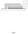
- FIG. 1 is a schematic view of a mesoscopic solar cell based on perovskite light absorption materials of an exemplary embodiment of the invention.
- FIG. 1 Structure of a mesoscopic solar cell of the invention is illustrated in FIG. 1 , where the cell comprises, from the top to the bottom, a conductive substrate 1, a hole blocking layer 2, a mesoporous nanocrystalline layer 3, an insulation separating layer 4, and a hole collecting layer 5.
- the mesoporous nanocrystalline layer 3 and the insulation separating layer 4 are nano oxide films.
- the nano oxide film is selecting from the group of titania, zirconia, alumina Stannum, Zinc, nickel and silica.
- the mesoporous nanocrystalline layer, the insulation separating layer, and the hole collecting layer are prepared by screen-printing layer by layer.
- the mesoporous nanocrystalline layer filled with the perovskite semiconductor materials becomes an active mesoporous nanocrystalline layer as the photoanode of the cell, and the insulation separating layer filled with the perovskite semiconductor materials becomes the hole transport layer transporting holes to the hole collecting layer.
- the titania layer has a grain size of 18 nm with a thickness of around 1 ⁇ m
- the insulation separating zirconia layer has a grain size of 20 nm with a thickness of 1 ⁇ m.
- the carbon-electrode hole collecting layer is a mesoporous conductive film made of graphite and carbon black with a thickness of approximately 10 ⁇ m.
- Certain amount (for example 4 ⁇ L) of methylamine lead iodine (CH 3 NH 3 Pbl 3 ) precursor solution (30 wt.%) is added on the mesoporous conductive film drop by drop, kept for 1 minute until it sufficiently penetrates in the titania mesoporous nanocrystalline layer, and finally dried at a certain temperature (for example 50°C).
- a certain temperature for example 50°C.
- the mesoporous nanocrystalline layer 3 and the insulation separating layer 4 are nano oxide films
- the mesoporous nanocrystalline layer 3 is preferably titania mesoporous nanocrystalline layer, but not limited to titania
- the grain size also is not limited to 18 nm
- the insulation separating layer 4 is preferably zirconia
- the grain size and thickness also are not limited to the above examples, and can be adjusted as required (for example 50 nm-10 ⁇ m).
- the hole collecting layer 5 is an electrode layer made of mesoporous materials, and preferably high work function electrode materials comprising carbon, indium tin oxide and so on, but not limited to these materials.
- a chemical formula of the perovskite semiconductor material is ABX 3 , where A is selecting from the group of alkylamine and an alkali element, B is selecting from the group of lead and tin, and X is selecting from the group of iodine, bromide and chlorine, and preferably methylamine lead iodine (CH 3 NH 3 Pbl 3 ).
Landscapes
- Chemical & Material Sciences (AREA)
- Engineering & Computer Science (AREA)
- Materials Engineering (AREA)
- Inorganic Chemistry (AREA)
- Physics & Mathematics (AREA)
- Electromagnetism (AREA)
- Photovoltaic Devices (AREA)
- Hybrid Cells (AREA)
- Manufacturing & Machinery (AREA)
Abstract
Description
- The invention relates to a field of solar cell technology, and more particularly, to a mesoscopic solar cell.
- A mesoscopic solar cell is a type of solar cell using a mesoporous nanocrystalline material as the photoanode. In this type of solar cell, light absorption materials are attached to a mesoporous nanocrystalline electrode as photoanodes, the photoelectrons are injected into the mesoporous nanocrystalline electrode and the holes are transported to a hole collecting layer via a hole transport layer to form photocurrent. Since the mesoporous nanocrystalline electrode has a large specific surface area, it can absorb a plenty of absorbing materials to obtain comparatively large photocurrent, and thus featuring an extremely high theoretical efficiency.
- Semiconductor nanocrystalline light absorption materials have been widely used in the field of mesoscopic solar cells for a long time, this is because that the semiconductor nanocrystalline light absorption material has a comparatively large optical section, and the band gap of the material may be changed by adjusting the crystal size within a certain range which related to the change of the open circuit voltage of the cell. The solar cell based on the semiconductor nanocrystalline light absorption material has a very high theoretical efficiency, although the material still faces several problems, such as poor stability, a short carrier recombination time and so on.
- As a new semiconductor perovskite light absorption material, there are several advantages with methylamine lead iodine (CH3NH3Pbl3), such as a wide light absorption range, a high light absorption coefficient, a long carrier recombination time, good stability and so on. At present, the all-solid-state mesoscopic solar cell based on this type of perovskite light absorption material may have a photoelectric conversion efficiency up to 12.3%. However, so far the cell using the perovskite semiconductor material as a light absorption material normally applys a p-type semiconductor material as a hole transport layer, and noble metals prepared by a vapor deposition method as counter electrodes to collect holes. The use of organic semiconductor materials requires a more advanced sealing process, which may affect the long-term stability of the cell to some extent. Moreover, vapor deposition of the noble metal electrodes may on one hand greatly increase the cost of cell preparation, and on the other hand severely restrict the large-scale production and application thereof.
- In view of the above-described problems, it is one objective of the invention to provide a mesoscopic solar cell based on perovskite light absorption materials and a preparation method. The solar cells are capable of directly transporting holes to a hole collecting layer by the hole conductivity of the perovskite semiconductor materials, which solves the problems of poor stability, high requirement for the sealing process of the cell, and high cost in the conventional solar cells.
- To achieve the above objective, in accordance with one embodiment of the invention, there is provided a mesoscopic solar cell based on perovskite light absorption materials, comprising a hole blocking layer, a mesoporous nanocrystalline layer, an insulation separating layer, and a hole collecting layer that sequentially layed on a conductive substrate. The mesoporous nanocrystalline layer, the insulation separating layer and the hole collecting layer are filled with perovskite semiconductor materials.
- In a class of this embodiment, the mesoporous nanocrystalline layer becomes an active light absorption layer after being filled with the perovskite semiconductor materials.
- In a class of this embodiment, the mesoporous nanocrystalline layer is a mesoporous inorganic nano oxide film.
- In a class of this embodiment, the insulation separating layer becomes a hole transport layer after being filled with said perovskite semiconductor materials.
- In a class of this embodiment, the insulation separating layer is a mesoporous inorganic nano oxide film.
- In a class of this embodiment, the hole blocking layer is a compact titania film.
- In a class of this embodiment, the perovskite semiconductor material is ABX3, where A is alkylamine or an alkali element, B is lead or tin, and X is selecting from the group of iodine, bromide and chlorine.
- In a class of this embodiment, the perovskite semiconductor material is preferably methylamine lead iodine (CH3NH3Pbl3).
- In a class of this embodiment, the inorganic and mesoporous nano oxide is selecting from the group of titania, zirconia, alumina, Stannum, Zinc, nickel and silica.
- In accordance with another embodiment of the invention, there is provided a method for preparing a mesoscopic solar cell based on perovskite light absorption materials, comprising steps of:
- 1) preparing a hole blocking layer on a conductive substrate;
- 2) preparing a mesoporous nanocrystalline layer, an insulation separating layer and a hole collecting layer on the hole blocking layer layer by layer and sintering; and
- 3) drop-coating precursor solution on the hole collecting layer so that it penetrates the pores of the mesoporous nanocrystalline layer through the hole collecting layer from the top to the bottom, and drying thereby obtaining a mesoscopic solar cell.
- In a class of this embodiment, the mesoporous nanocrystalline layer and the insulation separating layer are inorganic and mesoporous nano oxide films.
- In a class of this embodiment, the mesoporous nanocrystalline layer, the insulation separating layer, and the hole collecting layer are laminatedly prepared by screen-printing or doctor-blading.
- In a class of this embodiment, the hole blocking layer is a compact titania film.
- In a class of this embodiment, the perovskite semiconductor material is ABX3, where A is alkylamine or an alkali element, B is lead or tin, and X is selecting from the group of iodine, bromide and chlorine, and preferably methylamine lead iodine (CH3NH3Pbl3).
- In a class of this embodiment, the mesoporous inorganic nano oxide is selecting from the group of titania, zirconia, alumina, and silica.
- In a class of this embodiment, the method further comprises a step of filling an auxiliary p-type semiconductor thereby optimizing the hole transport property of the mesoporous nanocrystalline layer, insulation separating layer and the hole collecting layer after step (3).
- The solar cell of the invention comprises a conductive substrate, a hole blocking layer, a mesoporous nanocrystalline layer, an insulation separating layer, and a hole collecting layer. The mesoporous nanocrystalline layer, insulation separating layer and hole collecting layer in the above-mentioned step (2) are prepared by screen-printing, which requires no vacuum environment compared with a conventional vapor deposition method, and thus being capable of simplifying the preparation of the cell, and reducing production cost thereof.
- The mesoporous inorganic nano oxide of the invention is selecting from the group of titania, zirconia, alumina, Stannum, Zinc, nickel and silica, and a grain size thereof is preferably 10-400 nm. The hole collecting layer is preferably made of a high work function electrode material such as carbon, indium tin oxide and so on. A thickness of the film is preferably 50 nm-10 µm, and a sintering temperature is 400-500°C.
- To summarize, the mesoscopic solar cell of the invention is prepared by a fully screen-printing method, in which perovskite nanocrystalline is used as an active light absorption material, the hole transport layer is formed in the insulation separating layer by utilizing the hole transport property of the perovskite to directly transport holes to the hole collecting layer, and thus no organic p-type material is used. In addition, comparatively cheap materials, such as mesoporous carbon, are used as the hole collecting layer, which effectively simplifies the preparation process of the solar cell, reduces production cost thereof, and enables the invention to have a good industrialization prospect.
- The invention is described hereinbelow with reference to accompanying drawings, in which
FIG. 1 is a schematic view of a mesoscopic solar cell based on perovskite light absorption materials of an exemplary embodiment of the invention. - In the figure, the following reference numbers are used: 1. Conductive substrate; 2. Hole blocking layer; 3. Mesoporous nanocrystalline layer; 4. Insulation separating layer; 5. Hole collecting layer.
- For further illustrating the invention, experiments detailing an epoxy caulking adhesive are described below. It should be noted that the following examples are intended to describe and not to limit the invention.
- Structure of a mesoscopic solar cell of the invention is illustrated in
FIG. 1 , where the cell comprises, from the top to the bottom, aconductive substrate 1, ahole blocking layer 2, a mesoporousnanocrystalline layer 3, an insulation separatinglayer 4, and a hole collectinglayer 5. - The mesoporous
nanocrystalline layer 3, the insulation separatinglayer 4 and the hole collectinglayer 5 are filled with perovskite semiconductor materials. The mesoporousnanocrystalline layer 3 becomes an active light absorption layer after being filled with the perovskite semiconductor materials, and the insulation separatinglayer 4 becomes a hole transport layer after being filled with the perovskite semiconductor materials. - In addition, the mesoporous
nanocrystalline layer 3 and the insulation separatinglayer 4 are nano oxide films. For example, the nano oxide film is selecting from the group of titania, zirconia, alumina Stannum, Zinc, nickel and silica. - Preferably, the mesoporous nanocrystalline layer, the insulation separating layer, and the hole collecting layer are prepared by screen-printing layer by layer.
- After sintering, the mesoporous nanocrystalline layer filled with the perovskite semiconductor materials becomes an active mesoporous nanocrystalline layer as the photoanode of the cell, and the insulation separating layer filled with the perovskite semiconductor materials becomes the hole transport layer transporting holes to the hole collecting layer.
- After being filled with the perovskite semiconductor materials, the insulation separating layer being the nano oxide film can replace a conventional organic p-type semiconductor material and operates as a hole transport layer of the cell due to its hole transport capability. Moreover, the invention uses comparatively cheap materials, such as mesoporous carbon, as the hole collecting layer, and utilizes hole transport property of the perovskite semiconductor materials to transport holes to the hole collecting layer, which avoid the use of the organic p-type material.
- A method for preparing the mesoscopic solar cell of the invention will be described in details hereinafter with reference to specific examples:
- Firstly conductive glass is used as the
conductive substrate 1, then a compact titania layer 2 (with a thickness of 50 nm, for example) is deposited on the substrate, and finally a titania mesoporousnanocrystalline layer 3, a zirconia insulation separatinglayer 4, a carbon-electrode hole collectinglayer 5 are sequentially prepared by screen-printing from the bottom to the top. - For example, the titania layer has a grain size of 18 nm with a thickness of around 1 µm, and the insulation separating zirconia layer has a grain size of 20 nm with a thickness of 1 µm. The carbon-electrode hole collecting layer is a mesoporous conductive film made of graphite and carbon black with a thickness of approximately 10 µm. Certain amount (for example 4 µL) of methylamine lead iodine (CH3NH3Pbl3) precursor solution (30 wt%) is added on the mesoporous conductive film drop by drop, kept for 1 minute until it sufficiently penetrates in the titania mesoporous nanocrystalline layer, and finally dried at a certain temperature (for example 50°C). Test results indicate that the obtained solar cell has an efficiency of 6.64% under simulated sunlight of 100 mW/cm2.
- Firstly conductive glass is used as the
conductive substrate 1, then a compact titania layer 2 (with a thickness of 50 nm, for example) is deposited on the substrate, and finally a titaniamesoporous nanocrystalline layer 3, an aluminainsulation separating layer 4, a carbon-electrodehole collecting layer 5 are sequentially prepared by screen-printing from the bottom to the top. - For example, the titania layer has a grain size of 18 nm with a thickness of around 1 µm, and the insulation separating alumina layer has a grain size of 20 nm with a thickness of 1 µm. The carbon-electrode hole collecting layer is a mesoporous conductive film made of graphite and carbon black with a thickness of approximately 10 µm. Certain amount (for example 4 µL) of methylamine lead iodine (CH3NH3Pbl3) precursor solution (30 wt%) is added on the mesoporous conductive film drop by drop, kept for 1 minute until it sufficiently penetrates in the titania mesoporous nanocrystalline layer, and finally dried at a certain temperature (for example 50°C). Test results indicate that the obtained solar cell has an efficiency of 6.03% under simulated sunlight of 100 mW/cm2.
- Firstly conductive glass is used as the
conductive substrate 1, then a compact titania layer 2 (with a thickness of 50 nm, for example) is deposited on the substrate, and finally a titaniamesoporous nanocrystalline layer 3, a zirconiainsulation separating layer 4, a carbon-electrodehole collecting layer 5 are sequentially prepared by screen-printing from the bottom to the top. - For example, the titania layer has a grain size of 18 nm with a thickness of around 1 µm, and the insulation separating zirconia layer has a grain size of 20 nm with a thickness of 1 µm. The carbon-electrode hole collecting layer is a mesoporous conductive film made of graphite and carbon black with a thickness of approximately 10 µm. Certain amount (for example 4 µL) of methylamine lead iodine/bromide (CH3NH3Pbl2Br) precursor solution (30 wt%) is added on the mesoporous conductive film drop by drop, kept for 1 minute until it sufficiently penetrates in the titania mesoporous nanocrystalline layer, and finally dried at a certain temperature (for example 50°C). Test results indicate that the obtained solar cell has an efficiency of 5.87% under simulated sunlight of 100 mW/cm2.
- Firstly conductive glass is used as the
conductive substrate 1, then a compact titania layer 2 (with a thickness of 50 nm, for example) is deposited on the substrate, and finally a titaniamesoporous nanocrystalline layer 3, a zirconiainsulation separating layer 4, a indium-tin-oxide-electrodehole collecting layer 5 are sequentially prepared by screen-printing from the bottom to the top. - For example, the titania layer has a grain size of 18 nm with a thickness of around 1 µm, and the insulation separating zirconia layer has a grain size of 20 nm with a thickness of 1 µm. The indium-tin-oxide-electrode hole collecting layer is a mesoporous conductive film made of indium tin oxide nanocrystalline and having a thickness of approximately 10 µm. Certain amount (for example 4 µL) of methylamine lead iodine (CH3NH3Pbl3) precursor solution (30 wt.%) is added on the mesoporous conductive film drop by drop, kept for 1 minute until it sufficiently penetrates in the titania mesoporous nanocrystalline layer, and finally dried at a certain temperature (for example 50°C). Test results indicate that the obtained solar cell has an efficiency of 5.15% under simulated sunlight of 100 mW/cm2.
- In the above-mentioned examples, the
conductive substrate 1 is preferably conductive glass or conductive plastics. Thehole blocking layer 2 is an inorganic metal oxide film, and preferably a compact titania film with a thickness of 50 nm, but not limited to the titania film, and the thickness can be adjusted as required (for example 50 nm-10 µm). Themesoporous nanocrystalline layer 3 and theinsulation separating layer 4 are nano oxide films, themesoporous nanocrystalline layer 3 is preferably titania mesoporous nanocrystalline layer, but not limited to titania, the grain size also is not limited to 18 nm, theinsulation separating layer 4 is preferably zirconia, and the grain size and thickness also are not limited to the above examples, and can be adjusted as required (for example 50 nm-10 µm). Thehole collecting layer 5 is an electrode layer made of mesoporous materials, and preferably high work function electrode materials comprising carbon, indium tin oxide and so on, but not limited to these materials. - A chemical formula of the perovskite semiconductor material is ABX3, where A is selecting from the group of alkylamine and an alkali element, B is selecting from the group of lead and tin, and X is selecting from the group of iodine, bromide and chlorine, and preferably methylamine lead iodine (CH3NH3Pbl3).
- While particular embodiments of the invention have been shown and described, it will be obvious to those skilled in the art that changes and modifications may be made without departing from the invention in its broader aspects, and therefore, the aim in the appended claims is to cover all such changes and modifications as fall within the true spirit and scope of the invention.
Claims (10)
- A mesoscopic solar cell based on perovskite light absorption materials, comprising a conductive substrate (1), as well as a hole blocking layer (2), a mesoporous nanocrystalline layer (3), an insulation separating layer (4), and a hole collecting layer (5) sequentially laminated on the conductive substrate (1);
characterized in that
the perovskite semiconductor materials are filled in the mesoporous nanocrystalline layer (3), insulation separating layer (4) and hole collecting layer (5), which enables the mesoporous nanocrystalline layer (3) to be an active light absorption layer operating as a photoanode, and the insulation separating layer (4) to be a hole transporting layer of the solar cell. - The mesoscopic solar cell based on perovskite light absorption materials of claim 1, characterized in that the mesoporous nanocrystalline layer (3) and insulation separating layer (4) are mesoporous inorganic nano oxide films.
- The mesoscopic solar cell based on perovskite light absorption materials of claim 2, characterized in that the mesoporous inorganic nano oxide film is selecting from the group of titania, zirconia, alumina, Stannum, Zinc, nickel and silica.
- The mesoscopic solar cell based on perovskite light absorption materials of any one of claims 1 to 3, characterized in that the perovskite semiconductor material is ABX3, where A is alkylamine or an alkali element, B is lead or tin, and X is selecting from the group of iodine, bromide and chlorine.
- The mesoscopic solar cell based on perovskite light absorption materials of any one of claims 1 to 4, characterized in that the hole blocking layer (5) is a compact titania film.
- The mesoscopic solar cell based on perovskite light absorption materials of any one of claims 1 to 5, characterized in that the filling of perovskite semiconductor materials is taken through the way that the perovskite precursor solution drop-casted on the hole collecting layer (5), and penetrates the pores of the mesoporous nanocrystalline layer (3) through the hole collecting layer (5) from the top to the bottom.
- A method for preparing a mesoscopic solar cell based on perovskite light absorption materials, comprising steps of:1) 1 preparing a hole blocking layer (2) on a conductive substrate (1);2) preparing a mesoporous nanocrystalline layer (3), an insulation separating layer (4) and a hole collecting layer (5) on the hole blocking layer (2) layer by layer and sintering; and3) drop-coating precursor solution on the hole collecting layer (5) so that it penetrates the pores of the mesoporous nanocrystalline layer (3) through the hole collecting layer (5) from the top to the bottom, and drying thereby obtaining a mesoscopic solar cell.
- The method for claim 7, characterized in that the mesoporous nanocrystalline layer (3) and the insulation separating layer (4) are mesoporous inorganic nano oxide films.
- The method for claim 7 or 8, characterized in that the mesoporous nanocrystalline layer (3), the insulation separating layer (4), and the hole collecting layer (5) are prepared layer by layer by screen-printing or doctor-blading.
- The method for any one of claims 7 to 9, further comprising filling an p-type semiconductor thereby optimizing the hole transport property of the mesoporous nanocrystalline layer (3), the insulation separating layer (4) and the hole collecting layer (5) after step (3).
Applications Claiming Priority (2)
| Application Number | Priority Date | Filing Date | Title |
|---|---|---|---|
| CN201310297115.7A CN103441217B (en) | 2013-07-16 | 2013-07-16 | Jie based on perovskite light absorbent sees solar cell and preparation method thereof |
| PCT/CN2014/072510 WO2015007094A1 (en) | 2013-07-16 | 2014-02-25 | Mesoscopic solar cell based on perovskite light absorption material and preparation method thereof |
Publications (3)
| Publication Number | Publication Date |
|---|---|
| EP3024044A1 true EP3024044A1 (en) | 2016-05-25 |
| EP3024044A4 EP3024044A4 (en) | 2016-07-20 |
| EP3024044B1 EP3024044B1 (en) | 2019-04-10 |
Family
ID=49694901
Family Applications (1)
| Application Number | Title | Priority Date | Filing Date |
|---|---|---|---|
| EP14825987.2A Active EP3024044B1 (en) | 2013-07-16 | 2014-02-25 | Mesoscopic solar cell based on perovskite light absorption material and preparation method thereof |
Country Status (5)
| Country | Link |
|---|---|
| US (2) | US10199528B2 (en) |
| EP (1) | EP3024044B1 (en) |
| JP (1) | JP6267790B2 (en) |
| CN (1) | CN103441217B (en) |
| WO (1) | WO2015007094A1 (en) |
Families Citing this family (56)
| Publication number | Priority date | Publication date | Assignee | Title |
|---|---|---|---|---|
| CN103441217B (en) * | 2013-07-16 | 2015-11-04 | 华中科技大学 | Jie based on perovskite light absorbent sees solar cell and preparation method thereof |
| CN103490011B (en) * | 2013-09-30 | 2016-08-17 | 中国科学院物理研究所 | Perovskite-based thin film solar cell and preparation method thereof |
| CN104733183B (en) * | 2013-12-19 | 2017-10-03 | 清华大学 | Ca-Ti ore type solar cell and preparation method thereof |
| CN103681886B (en) * | 2013-12-26 | 2017-09-22 | 中国科学院物理研究所 | Shelf layer for perovskite-based thin film solar cell and preparation method thereof |
| CN103956392A (en) * | 2014-02-13 | 2014-07-30 | 大连七色光太阳能科技开发有限公司 | Perovskite-type battery based on carbon counter electrode and preparation method thereof |
| CN103794377B (en) * | 2014-02-21 | 2017-01-25 | 南京大学昆山创新研究院 | Dye-sensitized solar cell (DSSC) photo-anode and manufacturing method and application thereof |
| GB201405095D0 (en) * | 2014-03-21 | 2014-05-07 | Oxford Photovoltaics Ltd | Structure of an optoelectronic device |
| CN103904218A (en) * | 2014-03-28 | 2014-07-02 | 中国科学院上海技术物理研究所 | Perovskite thin-film solar cell structure based on metal particles |
| CN104979421B (en) * | 2014-04-11 | 2017-09-26 | 中国科学院大连化学物理研究所 | A kind of lamination solar cell |
| CN104022226B (en) * | 2014-05-14 | 2017-07-28 | 中国科学院物理研究所 | Perovskite-based thin film solar cell and preparation method thereof |
| CN104091889B (en) * | 2014-07-24 | 2015-08-05 | 华中科技大学 | Semiconductor perovskite solar cell and preparation method thereof |
| CN104124291B (en) * | 2014-07-24 | 2016-08-31 | 华中科技大学 | A kind of perovskite solar cell and preparation method thereof |
| US10297754B2 (en) * | 2014-08-01 | 2019-05-21 | International Business Machines Corporation | Techniques for perovskite layer crystallization |
| CN104124295A (en) * | 2014-08-12 | 2014-10-29 | 中国乐凯集团有限公司 | Planar heterogeneous perovskite solar cell and preparation method thereof |
| TWI527259B (en) | 2014-08-13 | 2016-03-21 | 國立清華大學 | Method for manufacturing perovskite solar cell |
| CN104157788B (en) * | 2014-08-19 | 2017-03-29 | 武汉大学 | A kind of perovskite thin-film photovoltaic cell based on SnO2 and preparation method thereof |
| CN104332560B (en) * | 2014-09-04 | 2017-01-11 | 武汉大学 | Preparation method of chlorine-bromine-iodine-mixing perovskite light absorption layer material |
| CN105655422A (en) * | 2014-11-12 | 2016-06-08 | 东莞日阵薄膜光伏技术有限公司 | Dual-junction perovskite/CIGS solar cells |
| CN104538552A (en) * | 2014-12-30 | 2015-04-22 | 南京信息工程大学 | Perovskite solar cell and manufacturing method thereof |
| CN104576930B (en) * | 2015-01-06 | 2017-05-03 | 宁波大学 | Perovskite solar cell and manufacturing method of perovskite solar cell |
| JP6742693B2 (en) * | 2015-02-17 | 2020-08-19 | 大阪瓦斯株式会社 | Inorganic photoelectric conversion device that can be manufactured by non-vacuum process |
| JP6732405B2 (en) * | 2015-02-24 | 2020-07-29 | 大阪瓦斯株式会社 | Perovskite solar cell and method of manufacturing the same |
| JP6339037B2 (en) * | 2015-03-18 | 2018-06-06 | 株式会社東芝 | Photoelectric conversion element and manufacturing method thereof |
| WO2016186317A1 (en) * | 2015-05-18 | 2016-11-24 | 고려대학교 산학협력단 | Perovskite solar cell module |
| CN105405973A (en) * | 2015-10-30 | 2016-03-16 | 华中科技大学 | Mesoscopic solar cell based on perovskite-kind light absorption material and preparation method thereof |
| US10775671B2 (en) * | 2015-12-23 | 2020-09-15 | Avantama Ag | Display device |
| CN105826473B (en) * | 2016-05-12 | 2019-06-21 | 东莞市联洲知识产权运营管理有限公司 | A kind of perovskite solar cell and preparation method thereof |
| WO2018011597A1 (en) * | 2016-07-15 | 2018-01-18 | Cristal Pigment Uk Limited | Solar cell materials for increased efficiency |
| BR112019002512A2 (en) * | 2016-09-21 | 2019-05-14 | Sekisui Chemical Co., Ltd | solar cell |
| KR102629585B1 (en) | 2016-10-04 | 2024-01-25 | 삼성전자주식회사 | Photoelectric conversion device and imaging device including the same |
| CN106847956B (en) * | 2017-03-08 | 2018-12-07 | 中国工程物理研究院材料研究所 | A kind of preparation method of the radiation detector based on full-inorganic perovskite monocrystalline |
| TWI651862B (en) * | 2017-06-05 | 2019-02-21 | 國立成功大學 | Solar cell manufacturing method |
| CN107482119A (en) * | 2017-06-29 | 2017-12-15 | 华中光电技术研究所(中国船舶重工集团公司第七七研究所) | A kind of perovskite solar cell and preparation method thereof |
| CN109698251B (en) | 2017-10-24 | 2020-05-19 | 华中科技大学 | Ferroelectric enhanced solar cell and preparation method thereof |
| CN110350093B (en) * | 2018-04-08 | 2021-07-27 | 华中科技大学 | A method for preparing solar cell light absorbing layer based on melting method and its application |
| CN110660918B (en) * | 2018-06-28 | 2022-09-06 | 湖北万度光能有限责任公司 | Perovskite solar cell packaging method |
| JP2020088316A (en) * | 2018-11-30 | 2020-06-04 | 国立大学法人東京工業大学 | Laminated body, solar cell, and method for manufacturing solar cell |
| CN110473973A (en) * | 2019-07-17 | 2019-11-19 | 北京大学深圳研究生院 | The interface post-processing approach and solar battery of carbon-based perovskite solar battery |
| US20230180490A1 (en) * | 2020-04-03 | 2023-06-08 | Yissum Research Development Company Of The Hebrew University Of Jerusalem Ltd. | Printable hole conductor free mesoporous indium tin oxide based perovskite solar cells |
| JP2022031598A (en) * | 2020-08-08 | 2022-02-21 | 紀州技研工業株式会社 | Mesoscopic photoelectric conversion element using perovskite compound and manufacturing method of the same |
| CN112071988B (en) * | 2020-09-02 | 2021-12-10 | 西北工业大学 | Preparation method of full-screen printing perovskite solar cell |
| CN112071991B (en) * | 2020-09-02 | 2022-02-08 | 西北工业大学 | Method for preparing perovskite film through screen printing |
| CN111953281A (en) * | 2020-09-16 | 2020-11-17 | 中北大学 | Photoelectric-thermoelectric composite power generation device and system |
| CN112151679B (en) * | 2020-09-29 | 2022-12-09 | 西北工业大学 | A kind of nano crystal composite perovskite solar cell and its preparation method |
| JP7827054B2 (en) * | 2021-02-24 | 2026-03-10 | 日本ゼオン株式会社 | Photoelectric conversion module and manufacturing method thereof |
| JP2022149865A (en) * | 2021-03-25 | 2022-10-07 | 紀州技研工業株式会社 | Mesoscopic photoelectric conversion element using perovskite compound, power generation system using the same, and control method thereof |
| CN113363391A (en) * | 2021-05-24 | 2021-09-07 | 桂林电子科技大学 | Carbon-based full-printing perovskite solar cell based on ionic liquid additive and preparation method thereof |
| TWI803049B (en) * | 2021-11-11 | 2023-05-21 | 國立雲林科技大學 | Nano-structure-modified organic component manufacturing method and structure thereof |
| CN115165495B (en) * | 2022-07-08 | 2025-03-28 | 湖北万度光能有限责任公司 | A method for characterizing the morphology of semiconductor materials in mesopores |
| WO2024029426A1 (en) * | 2022-08-01 | 2024-02-08 | シャープ株式会社 | Perovskite solar cell and method for producing same |
| CN115988941B (en) * | 2022-12-13 | 2025-06-27 | 湖北万度光能有限责任公司 | Laser sintering perovskite solar cell and preparation method thereof |
| CN117295372A (en) * | 2023-09-11 | 2023-12-26 | 武汉万度光能研究院有限责任公司 | A kind of perovskite solar cell and preparation method |
| CN117818230A (en) * | 2024-01-31 | 2024-04-05 | 中国科学院上海硅酸盐研究所 | Method for preparing perovskite light absorption layer by pseudo screen printing process |
| JP7702514B1 (en) * | 2024-02-27 | 2025-07-03 | シャープエネルギーソリューション株式会社 | Photoelectric conversion element and its manufacturing method |
| CN118497823B (en) * | 2024-07-16 | 2024-11-05 | 三峡智能工程有限公司 | A semiconductor anode for a light-energy electrolytic water cell and a method and system for preparing the same |
| CN119855450B (en) * | 2024-12-31 | 2025-11-14 | 华电电力科学研究院有限公司 | A perovskite solar cell and its fabrication method |
Family Cites Families (13)
| Publication number | Priority date | Publication date | Assignee | Title |
|---|---|---|---|---|
| EP0858669B1 (en) * | 1995-10-31 | 1999-11-03 | Ecole Polytechnique Féderale de Lausanne (EPFL) | A battery of photovoltaic cells and process for manufacturing the same |
| JP2002299063A (en) * | 2001-04-03 | 2002-10-11 | Japan Science & Technology Corp | Electroluminescent device using lead bromide-based layered perovskite compound as light emitting layer |
| US20030015728A1 (en) * | 2001-07-17 | 2003-01-23 | Motorola, Inc. | Photonic biasing and integrated solar charging networks for integrated circuits |
| KR100844871B1 (en) * | 2007-04-06 | 2008-07-09 | 경북대학교 산학협력단 | Dye-sensitized solar cell dye and solar cell using same |
| US20090056791A1 (en) * | 2007-06-22 | 2009-03-05 | William Matthew Pfenninger | Solar modules with enhanced efficiencies via use of spectral concentrators |
| US9496442B2 (en) * | 2009-01-22 | 2016-11-15 | Omnipv | Solar modules including spectral concentrators and related manufacturing methods |
| EP2421084B1 (en) * | 2009-04-15 | 2014-03-19 | Sharp Kabushiki Kaisha | Dye-sensitized solar cell and dye-sensitized solar cell module |
| US20110088758A1 (en) * | 2009-10-19 | 2011-04-21 | Tadao Yagi | Glass paste composition, electrode substrate prepared using same, method of preparing electrode substrate, and dye sensitized solar cell including electrode substrate |
| CN101740238B (en) * | 2010-03-12 | 2011-08-10 | 华中科技大学 | Dye-sensitized solar cell and preparation method thereof |
| GB201008144D0 (en) * | 2010-05-14 | 2010-06-30 | Solar Press Uk The Ltd | Surface modified electrode layers in organic photovoltaic cells |
| JP2012014849A (en) * | 2010-06-29 | 2012-01-19 | Sony Corp | Photoelectric conversion element, method for manufacturing the same, photoelectric conversion element module and method for manufacturing the same |
| KR101172374B1 (en) * | 2011-02-14 | 2012-08-08 | 성균관대학교산학협력단 | Dye-sensitized solar cell based on perovskite sensitizer and manufacturing method thereof |
| CN103441217B (en) * | 2013-07-16 | 2015-11-04 | 华中科技大学 | Jie based on perovskite light absorbent sees solar cell and preparation method thereof |
-
2013
- 2013-07-16 CN CN201310297115.7A patent/CN103441217B/en active Active
-
2014
- 2014-02-25 EP EP14825987.2A patent/EP3024044B1/en active Active
- 2014-02-25 WO PCT/CN2014/072510 patent/WO2015007094A1/en not_active Ceased
- 2014-02-25 JP JP2016522194A patent/JP6267790B2/en active Active
-
2015
- 2015-12-31 US US14/985,470 patent/US10199528B2/en active Active
-
2016
- 2016-06-29 US US15/197,743 patent/US9799790B2/en active Active
Also Published As
| Publication number | Publication date |
|---|---|
| JP2016523453A (en) | 2016-08-08 |
| CN103441217A (en) | 2013-12-11 |
| WO2015007094A1 (en) | 2015-01-22 |
| CN103441217B (en) | 2015-11-04 |
| US20160111575A1 (en) | 2016-04-21 |
| US9799790B2 (en) | 2017-10-24 |
| US20160315213A1 (en) | 2016-10-27 |
| EP3024044B1 (en) | 2019-04-10 |
| US10199528B2 (en) | 2019-02-05 |
| EP3024044A4 (en) | 2016-07-20 |
| JP6267790B2 (en) | 2018-01-24 |
Similar Documents
| Publication | Publication Date | Title |
|---|---|---|
| EP3024044B1 (en) | Mesoscopic solar cell based on perovskite light absorption material and preparation method thereof | |
| Zhao et al. | Numerical simulation of planar heterojunction perovskite solar cells based on SnO2 electron transport layer | |
| Foo et al. | Recent review on electron transport layers in perovskite solar cells | |
| Wang et al. | High‐efficiency flexible solar cells based on organometal halide perovskites | |
| Guchhait et al. | Over 20% efficient CIGS–perovskite tandem solar cells | |
| Lu et al. | A self‐powered and stable all‐perovskite photodetector–solar cell nanosystem | |
| Gonzalez-Pedro et al. | General working principles of CH3NH3PbX3 perovskite solar cells | |
| EP3172776B9 (en) | Mesoscopic framework for organic-inorganic perovskite based photoelectric conversion device and method for manufacturing the same | |
| Ke et al. | Efficient fully-vacuum-processed perovskite solar cells using copper phthalocyanine as hole selective layers | |
| KR102729439B1 (en) | Perovskite solar cell and tandem solar cell including the same | |
| Castro-Hermosa et al. | Stability issues pertaining large area perovskite and dye-sensitized solar cells and modules | |
| Liu et al. | Carbon Electrode Endows High‐Efficiency Perovskite Photovoltaics Affordable, Fully Printable, and Durable | |
| KR101723797B1 (en) | Perovskite-amorphous silicon heterojunction solar cell and method for preparing the same | |
| WO2020246074A1 (en) | Four-terminal tandem solar cell | |
| KR20150143010A (en) | Solar cell and method for manufacturing the same | |
| Xu et al. | Efficient monolithic solid-state dye-sensitized solar cell with a low-cost mesoscopic carbon based screen printable counter electrode | |
| CN112136225A (en) | Solar battery | |
| KR101694803B1 (en) | Perovskite solar cells comprising metal nanowire as photoelectrode, and the preparation method thereof | |
| CN204905305U (en) | A simplified methylamine iodide lead perovskite battery | |
| CN103426645B (en) | Utilize metal flexible DSSC and the manufacture method thereof of the metal substrate of dual coating | |
| TWI500175B (en) | Metal flexible dye-sensitized solar cell and method of manufacturing same | |
| KR102377621B1 (en) | Solar cell with improved stability against moisture and long-term stability | |
| CN109564822A (en) | Dye-sensitized solar cells and its manufacturing method | |
| JP2009009851A (en) | Photoelectric conversion device | |
| KR101422509B1 (en) | Metal flexible dye-sensitized solar cell with texturing azo glass transparent electrode and manufacturing method thereof |
Legal Events
| Date | Code | Title | Description |
|---|---|---|---|
| PUAI | Public reference made under article 153(3) epc to a published international application that has entered the european phase |
Free format text: ORIGINAL CODE: 0009012 |
|
| 17P | Request for examination filed |
Effective date: 20160114 |
|
| AK | Designated contracting states |
Kind code of ref document: A1 Designated state(s): AL AT BE BG CH CY CZ DE DK EE ES FI FR GB GR HR HU IE IS IT LI LT LU LV MC MK MT NL NO PL PT RO RS SE SI SK SM TR |
|
| AX | Request for extension of the european patent |
Extension state: BA ME |
|
| A4 | Supplementary search report drawn up and despatched |
Effective date: 20160622 |
|
| RIC1 | Information provided on ipc code assigned before grant |
Ipc: H01L 51/44 20060101ALI20160616BHEP Ipc: H01L 51/46 20060101AFI20160616BHEP Ipc: H01L 51/48 20060101ALI20160616BHEP |
|
| 17Q | First examination report despatched |
Effective date: 20160819 |
|
| DAX | Request for extension of the european patent (deleted) | ||
| STAA | Information on the status of an ep patent application or granted ep patent |
Free format text: STATUS: EXAMINATION IS IN PROGRESS |
|
| RAP1 | Party data changed (applicant data changed or rights of an application transferred) |
Owner name: WONDER SOLAR LIMITED LIABILITY COMPANY |
|
| GRAP | Despatch of communication of intention to grant a patent |
Free format text: ORIGINAL CODE: EPIDOSNIGR1 |
|
| STAA | Information on the status of an ep patent application or granted ep patent |
Free format text: STATUS: GRANT OF PATENT IS INTENDED |
|
| INTG | Intention to grant announced |
Effective date: 20181119 |
|
| GRAS | Grant fee paid |
Free format text: ORIGINAL CODE: EPIDOSNIGR3 |
|
| GRAA | (expected) grant |
Free format text: ORIGINAL CODE: 0009210 |
|
| STAA | Information on the status of an ep patent application or granted ep patent |
Free format text: STATUS: THE PATENT HAS BEEN GRANTED |
|
| AK | Designated contracting states |
Kind code of ref document: B1 Designated state(s): AL AT BE BG CH CY CZ DE DK EE ES FI FR GB GR HR HU IE IS IT LI LT LU LV MC MK MT NL NO PL PT RO RS SE SI SK SM TR |
|
| REG | Reference to a national code |
Ref country code: GB Ref legal event code: FG4D |
|
| REG | Reference to a national code |
Ref country code: CH Ref legal event code: EP Ref country code: AT Ref legal event code: REF Ref document number: 1119881 Country of ref document: AT Kind code of ref document: T Effective date: 20190415 |
|
| REG | Reference to a national code |
Ref country code: IE Ref legal event code: FG4D |
|
| REG | Reference to a national code |
Ref country code: DE Ref legal event code: R096 Ref document number: 602014044602 Country of ref document: DE |
|
| REG | Reference to a national code |
Ref country code: NL Ref legal event code: FP |
|
| REG | Reference to a national code |
Ref country code: CH Ref legal event code: NV Representative=s name: LANGPATENT ANWALTSKANZLEI IP LAW FIRM, CH |
|
| REG | Reference to a national code |
Ref country code: LT Ref legal event code: MG4D |
|
| REG | Reference to a national code |
Ref country code: AT Ref legal event code: MK05 Ref document number: 1119881 Country of ref document: AT Kind code of ref document: T Effective date: 20190410 |
|
| PG25 | Lapsed in a contracting state [announced via postgrant information from national office to epo] |
Ref country code: AL Free format text: LAPSE BECAUSE OF FAILURE TO SUBMIT A TRANSLATION OF THE DESCRIPTION OR TO PAY THE FEE WITHIN THE PRESCRIBED TIME-LIMIT Effective date: 20190410 Ref country code: ES Free format text: LAPSE BECAUSE OF FAILURE TO SUBMIT A TRANSLATION OF THE DESCRIPTION OR TO PAY THE FEE WITHIN THE PRESCRIBED TIME-LIMIT Effective date: 20190410 Ref country code: SE Free format text: LAPSE BECAUSE OF FAILURE TO SUBMIT A TRANSLATION OF THE DESCRIPTION OR TO PAY THE FEE WITHIN THE PRESCRIBED TIME-LIMIT Effective date: 20190410 Ref country code: NO Free format text: LAPSE BECAUSE OF FAILURE TO SUBMIT A TRANSLATION OF THE DESCRIPTION OR TO PAY THE FEE WITHIN THE PRESCRIBED TIME-LIMIT Effective date: 20190710 Ref country code: PT Free format text: LAPSE BECAUSE OF FAILURE TO SUBMIT A TRANSLATION OF THE DESCRIPTION OR TO PAY THE FEE WITHIN THE PRESCRIBED TIME-LIMIT Effective date: 20190910 Ref country code: HR Free format text: LAPSE BECAUSE OF FAILURE TO SUBMIT A TRANSLATION OF THE DESCRIPTION OR TO PAY THE FEE WITHIN THE PRESCRIBED TIME-LIMIT Effective date: 20190410 Ref country code: FI Free format text: LAPSE BECAUSE OF FAILURE TO SUBMIT A TRANSLATION OF THE DESCRIPTION OR TO PAY THE FEE WITHIN THE PRESCRIBED TIME-LIMIT Effective date: 20190410 Ref country code: LT Free format text: LAPSE BECAUSE OF FAILURE TO SUBMIT A TRANSLATION OF THE DESCRIPTION OR TO PAY THE FEE WITHIN THE PRESCRIBED TIME-LIMIT Effective date: 20190410 |
|
| PG25 | Lapsed in a contracting state [announced via postgrant information from national office to epo] |
Ref country code: LV Free format text: LAPSE BECAUSE OF FAILURE TO SUBMIT A TRANSLATION OF THE DESCRIPTION OR TO PAY THE FEE WITHIN THE PRESCRIBED TIME-LIMIT Effective date: 20190410 Ref country code: RS Free format text: LAPSE BECAUSE OF FAILURE TO SUBMIT A TRANSLATION OF THE DESCRIPTION OR TO PAY THE FEE WITHIN THE PRESCRIBED TIME-LIMIT Effective date: 20190410 Ref country code: BG Free format text: LAPSE BECAUSE OF FAILURE TO SUBMIT A TRANSLATION OF THE DESCRIPTION OR TO PAY THE FEE WITHIN THE PRESCRIBED TIME-LIMIT Effective date: 20190710 Ref country code: GR Free format text: LAPSE BECAUSE OF FAILURE TO SUBMIT A TRANSLATION OF THE DESCRIPTION OR TO PAY THE FEE WITHIN THE PRESCRIBED TIME-LIMIT Effective date: 20190711 Ref country code: PL Free format text: LAPSE BECAUSE OF FAILURE TO SUBMIT A TRANSLATION OF THE DESCRIPTION OR TO PAY THE FEE WITHIN THE PRESCRIBED TIME-LIMIT Effective date: 20190410 |
|
| PG25 | Lapsed in a contracting state [announced via postgrant information from national office to epo] |
Ref country code: IS Free format text: LAPSE BECAUSE OF FAILURE TO SUBMIT A TRANSLATION OF THE DESCRIPTION OR TO PAY THE FEE WITHIN THE PRESCRIBED TIME-LIMIT Effective date: 20190810 Ref country code: AT Free format text: LAPSE BECAUSE OF FAILURE TO SUBMIT A TRANSLATION OF THE DESCRIPTION OR TO PAY THE FEE WITHIN THE PRESCRIBED TIME-LIMIT Effective date: 20190410 |
|
| REG | Reference to a national code |
Ref country code: DE Ref legal event code: R097 Ref document number: 602014044602 Country of ref document: DE |
|
| PG25 | Lapsed in a contracting state [announced via postgrant information from national office to epo] |
Ref country code: DK Free format text: LAPSE BECAUSE OF FAILURE TO SUBMIT A TRANSLATION OF THE DESCRIPTION OR TO PAY THE FEE WITHIN THE PRESCRIBED TIME-LIMIT Effective date: 20190410 Ref country code: SK Free format text: LAPSE BECAUSE OF FAILURE TO SUBMIT A TRANSLATION OF THE DESCRIPTION OR TO PAY THE FEE WITHIN THE PRESCRIBED TIME-LIMIT Effective date: 20190410 Ref country code: EE Free format text: LAPSE BECAUSE OF FAILURE TO SUBMIT A TRANSLATION OF THE DESCRIPTION OR TO PAY THE FEE WITHIN THE PRESCRIBED TIME-LIMIT Effective date: 20190410 Ref country code: CZ Free format text: LAPSE BECAUSE OF FAILURE TO SUBMIT A TRANSLATION OF THE DESCRIPTION OR TO PAY THE FEE WITHIN THE PRESCRIBED TIME-LIMIT Effective date: 20190410 Ref country code: RO Free format text: LAPSE BECAUSE OF FAILURE TO SUBMIT A TRANSLATION OF THE DESCRIPTION OR TO PAY THE FEE WITHIN THE PRESCRIBED TIME-LIMIT Effective date: 20190410 |
|
| PLBE | No opposition filed within time limit |
Free format text: ORIGINAL CODE: 0009261 |
|
| STAA | Information on the status of an ep patent application or granted ep patent |
Free format text: STATUS: NO OPPOSITION FILED WITHIN TIME LIMIT |
|
| PG25 | Lapsed in a contracting state [announced via postgrant information from national office to epo] |
Ref country code: SM Free format text: LAPSE BECAUSE OF FAILURE TO SUBMIT A TRANSLATION OF THE DESCRIPTION OR TO PAY THE FEE WITHIN THE PRESCRIBED TIME-LIMIT Effective date: 20190410 Ref country code: IT Free format text: LAPSE BECAUSE OF FAILURE TO SUBMIT A TRANSLATION OF THE DESCRIPTION OR TO PAY THE FEE WITHIN THE PRESCRIBED TIME-LIMIT Effective date: 20190410 |
|
| 26N | No opposition filed |
Effective date: 20200113 |
|
| PG25 | Lapsed in a contracting state [announced via postgrant information from national office to epo] |
Ref country code: TR Free format text: LAPSE BECAUSE OF FAILURE TO SUBMIT A TRANSLATION OF THE DESCRIPTION OR TO PAY THE FEE WITHIN THE PRESCRIBED TIME-LIMIT Effective date: 20190410 |
|
| PG25 | Lapsed in a contracting state [announced via postgrant information from national office to epo] |
Ref country code: SI Free format text: LAPSE BECAUSE OF FAILURE TO SUBMIT A TRANSLATION OF THE DESCRIPTION OR TO PAY THE FEE WITHIN THE PRESCRIBED TIME-LIMIT Effective date: 20190410 |
|
| REG | Reference to a national code |
Ref country code: BE Ref legal event code: MM Effective date: 20200229 |
|
| PG25 | Lapsed in a contracting state [announced via postgrant information from national office to epo] |
Ref country code: MC Free format text: LAPSE BECAUSE OF FAILURE TO SUBMIT A TRANSLATION OF THE DESCRIPTION OR TO PAY THE FEE WITHIN THE PRESCRIBED TIME-LIMIT Effective date: 20190410 Ref country code: LU Free format text: LAPSE BECAUSE OF NON-PAYMENT OF DUE FEES Effective date: 20200225 |
|
| PG25 | Lapsed in a contracting state [announced via postgrant information from national office to epo] |
Ref country code: IE Free format text: LAPSE BECAUSE OF NON-PAYMENT OF DUE FEES Effective date: 20200225 |
|
| PG25 | Lapsed in a contracting state [announced via postgrant information from national office to epo] |
Ref country code: BE Free format text: LAPSE BECAUSE OF NON-PAYMENT OF DUE FEES Effective date: 20200229 |
|
| PG25 | Lapsed in a contracting state [announced via postgrant information from national office to epo] |
Ref country code: MT Free format text: LAPSE BECAUSE OF FAILURE TO SUBMIT A TRANSLATION OF THE DESCRIPTION OR TO PAY THE FEE WITHIN THE PRESCRIBED TIME-LIMIT Effective date: 20190410 Ref country code: CY Free format text: LAPSE BECAUSE OF FAILURE TO SUBMIT A TRANSLATION OF THE DESCRIPTION OR TO PAY THE FEE WITHIN THE PRESCRIBED TIME-LIMIT Effective date: 20190410 |
|
| PG25 | Lapsed in a contracting state [announced via postgrant information from national office to epo] |
Ref country code: MK Free format text: LAPSE BECAUSE OF FAILURE TO SUBMIT A TRANSLATION OF THE DESCRIPTION OR TO PAY THE FEE WITHIN THE PRESCRIBED TIME-LIMIT Effective date: 20190410 |
|
| REG | Reference to a national code |
Ref country code: DE Ref legal event code: R082 Ref document number: 602014044602 Country of ref document: DE |
|
| REG | Reference to a national code |
Ref country code: DE Ref legal event code: R079 Ref document number: 602014044602 Country of ref document: DE Free format text: PREVIOUS MAIN CLASS: H01L0051460000 Ipc: H10K0085000000 |
|
| PGFP | Annual fee paid to national office [announced via postgrant information from national office to epo] |
Ref country code: NL Payment date: 20260218 Year of fee payment: 13 |
|
| REG | Reference to a national code |
Ref country code: CH Ref legal event code: U11 Free format text: ST27 STATUS EVENT CODE: U-0-0-U10-U11 (AS PROVIDED BY THE NATIONAL OFFICE) Effective date: 20260323 |
|
| PGFP | Annual fee paid to national office [announced via postgrant information from national office to epo] |
Ref country code: GB Payment date: 20260206 Year of fee payment: 13 |
|
| PGFP | Annual fee paid to national office [announced via postgrant information from national office to epo] |
Ref country code: DE Payment date: 20260211 Year of fee payment: 13 |
|
| PGFP | Annual fee paid to national office [announced via postgrant information from national office to epo] |
Ref country code: FR Payment date: 20260206 Year of fee payment: 13 |
|
| PGFP | Annual fee paid to national office [announced via postgrant information from national office to epo] |
Ref country code: CH Payment date: 20260323 Year of fee payment: 13 |