EP3024024A1 - Semiconductor module - Google Patents
Semiconductor module Download PDFInfo
- Publication number
- EP3024024A1 EP3024024A1 EP14855368.8A EP14855368A EP3024024A1 EP 3024024 A1 EP3024024 A1 EP 3024024A1 EP 14855368 A EP14855368 A EP 14855368A EP 3024024 A1 EP3024024 A1 EP 3024024A1
- Authority
- EP
- European Patent Office
- Prior art keywords
- electrode
- jointing
- substrate
- metal plate
- flat plate
- Prior art date
- Legal status (The legal status is an assumption and is not a legal conclusion. Google has not performed a legal analysis and makes no representation as to the accuracy of the status listed.)
- Granted
Links
Images






Classifications
-
- H—ELECTRICITY
- H10—SEMICONDUCTOR DEVICES; ELECTRIC SOLID-STATE DEVICES NOT OTHERWISE PROVIDED FOR
- H10W—GENERIC PACKAGES, INTERCONNECTIONS, CONNECTORS OR OTHER CONSTRUCTIONAL DETAILS OF DEVICES COVERED BY CLASS H10
- H10W40/00—Arrangements for thermal protection or thermal control
- H10W40/20—Arrangements for cooling
- H10W40/25—Arrangements for cooling characterised by their materials
- H10W40/255—Arrangements for cooling characterised by their materials having a laminate or multilayered structure, e.g. direct bond copper [DBC] ceramic substrates
-
- H—ELECTRICITY
- H10—SEMICONDUCTOR DEVICES; ELECTRIC SOLID-STATE DEVICES NOT OTHERWISE PROVIDED FOR
- H10D—INORGANIC ELECTRIC SEMICONDUCTOR DEVICES
- H10D12/00—Bipolar devices controlled by the field effect, e.g. insulated-gate bipolar transistors [IGBT]
- H10D12/411—Insulated-gate bipolar transistors [IGBT]
-
- H—ELECTRICITY
- H10—SEMICONDUCTOR DEVICES; ELECTRIC SOLID-STATE DEVICES NOT OTHERWISE PROVIDED FOR
- H10D—INORGANIC ELECTRIC SEMICONDUCTOR DEVICES
- H10D30/00—Field-effect transistors [FET]
- H10D30/60—Insulated-gate field-effect transistors [IGFET]
-
- H—ELECTRICITY
- H10—SEMICONDUCTOR DEVICES; ELECTRIC SOLID-STATE DEVICES NOT OTHERWISE PROVIDED FOR
- H10W—GENERIC PACKAGES, INTERCONNECTIONS, CONNECTORS OR OTHER CONSTRUCTIONAL DETAILS OF DEVICES COVERED BY CLASS H10
- H10W70/00—Package substrates; Interposers; Redistribution layers [RDL]
- H10W70/20—Conductive package substrates serving as an interconnection, e.g. metal plates
-
- H—ELECTRICITY
- H10—SEMICONDUCTOR DEVICES; ELECTRIC SOLID-STATE DEVICES NOT OTHERWISE PROVIDED FOR
- H10W—GENERIC PACKAGES, INTERCONNECTIONS, CONNECTORS OR OTHER CONSTRUCTIONAL DETAILS OF DEVICES COVERED BY CLASS H10
- H10W70/00—Package substrates; Interposers; Redistribution layers [RDL]
- H10W70/60—Insulating or insulated package substrates; Interposers; Redistribution layers
- H10W70/62—Insulating or insulated package substrates; Interposers; Redistribution layers characterised by their interconnections
- H10W70/65—Shapes or dispositions of interconnections
-
- H—ELECTRICITY
- H10—SEMICONDUCTOR DEVICES; ELECTRIC SOLID-STATE DEVICES NOT OTHERWISE PROVIDED FOR
- H10W—GENERIC PACKAGES, INTERCONNECTIONS, CONNECTORS OR OTHER CONSTRUCTIONAL DETAILS OF DEVICES COVERED BY CLASS H10
- H10W90/00—Package configurations
-
- H—ELECTRICITY
- H10—SEMICONDUCTOR DEVICES; ELECTRIC SOLID-STATE DEVICES NOT OTHERWISE PROVIDED FOR
- H10W—GENERIC PACKAGES, INTERCONNECTIONS, CONNECTORS OR OTHER CONSTRUCTIONAL DETAILS OF DEVICES COVERED BY CLASS H10
- H10W90/00—Package configurations
- H10W90/701—Package configurations characterised by the relative positions of pads or connectors relative to package parts
-
- H—ELECTRICITY
- H10—SEMICONDUCTOR DEVICES; ELECTRIC SOLID-STATE DEVICES NOT OTHERWISE PROVIDED FOR
- H10W—GENERIC PACKAGES, INTERCONNECTIONS, CONNECTORS OR OTHER CONSTRUCTIONAL DETAILS OF DEVICES COVERED BY CLASS H10
- H10W72/00—Interconnections or connectors in packages
- H10W72/01—Manufacture or treatment
- H10W72/013—Manufacture or treatment of die-attach connectors
- H10W72/01321—Manufacture or treatment of die-attach connectors using local deposition
- H10W72/01323—Manufacture or treatment of die-attach connectors using local deposition in liquid form, e.g. by dispensing droplets or by screen printing
-
- H—ELECTRICITY
- H10—SEMICONDUCTOR DEVICES; ELECTRIC SOLID-STATE DEVICES NOT OTHERWISE PROVIDED FOR
- H10W—GENERIC PACKAGES, INTERCONNECTIONS, CONNECTORS OR OTHER CONSTRUCTIONAL DETAILS OF DEVICES COVERED BY CLASS H10
- H10W72/00—Interconnections or connectors in packages
- H10W72/01—Manufacture or treatment
- H10W72/016—Manufacture or treatment of strap connectors
-
- H—ELECTRICITY
- H10—SEMICONDUCTOR DEVICES; ELECTRIC SOLID-STATE DEVICES NOT OTHERWISE PROVIDED FOR
- H10W—GENERIC PACKAGES, INTERCONNECTIONS, CONNECTORS OR OTHER CONSTRUCTIONAL DETAILS OF DEVICES COVERED BY CLASS H10
- H10W72/00—Interconnections or connectors in packages
- H10W72/01—Manufacture or treatment
- H10W72/016—Manufacture or treatment of strap connectors
- H10W72/01661—Chemical or physical modification, e.g. by sintering or anodisation
-
- H—ELECTRICITY
- H10—SEMICONDUCTOR DEVICES; ELECTRIC SOLID-STATE DEVICES NOT OTHERWISE PROVIDED FOR
- H10W—GENERIC PACKAGES, INTERCONNECTIONS, CONNECTORS OR OTHER CONSTRUCTIONAL DETAILS OF DEVICES COVERED BY CLASS H10
- H10W72/00—Interconnections or connectors in packages
- H10W72/071—Connecting or disconnecting
- H10W72/073—Connecting or disconnecting of die-attach connectors
-
- H—ELECTRICITY
- H10—SEMICONDUCTOR DEVICES; ELECTRIC SOLID-STATE DEVICES NOT OTHERWISE PROVIDED FOR
- H10W—GENERIC PACKAGES, INTERCONNECTIONS, CONNECTORS OR OTHER CONSTRUCTIONAL DETAILS OF DEVICES COVERED BY CLASS H10
- H10W72/00—Interconnections or connectors in packages
- H10W72/071—Connecting or disconnecting
- H10W72/073—Connecting or disconnecting of die-attach connectors
- H10W72/07331—Connecting techniques
- H10W72/07334—Using a reflow oven
-
- H—ELECTRICITY
- H10—SEMICONDUCTOR DEVICES; ELECTRIC SOLID-STATE DEVICES NOT OTHERWISE PROVIDED FOR
- H10W—GENERIC PACKAGES, INTERCONNECTIONS, CONNECTORS OR OTHER CONSTRUCTIONAL DETAILS OF DEVICES COVERED BY CLASS H10
- H10W72/00—Interconnections or connectors in packages
- H10W72/071—Connecting or disconnecting
- H10W72/073—Connecting or disconnecting of die-attach connectors
- H10W72/07331—Connecting techniques
- H10W72/07336—Soldering or alloying
-
- H—ELECTRICITY
- H10—SEMICONDUCTOR DEVICES; ELECTRIC SOLID-STATE DEVICES NOT OTHERWISE PROVIDED FOR
- H10W—GENERIC PACKAGES, INTERCONNECTIONS, CONNECTORS OR OTHER CONSTRUCTIONAL DETAILS OF DEVICES COVERED BY CLASS H10
- H10W72/00—Interconnections or connectors in packages
- H10W72/071—Connecting or disconnecting
- H10W72/073—Connecting or disconnecting of die-attach connectors
- H10W72/07351—Connecting or disconnecting of die-attach connectors characterised by changes in properties of the die-attach connectors during connecting
- H10W72/07354—Connecting or disconnecting of die-attach connectors characterised by changes in properties of the die-attach connectors during connecting changes in dispositions
-
- H—ELECTRICITY
- H10—SEMICONDUCTOR DEVICES; ELECTRIC SOLID-STATE DEVICES NOT OTHERWISE PROVIDED FOR
- H10W—GENERIC PACKAGES, INTERCONNECTIONS, CONNECTORS OR OTHER CONSTRUCTIONAL DETAILS OF DEVICES COVERED BY CLASS H10
- H10W72/00—Interconnections or connectors in packages
- H10W72/071—Connecting or disconnecting
- H10W72/076—Connecting or disconnecting of strap connectors
-
- H—ELECTRICITY
- H10—SEMICONDUCTOR DEVICES; ELECTRIC SOLID-STATE DEVICES NOT OTHERWISE PROVIDED FOR
- H10W—GENERIC PACKAGES, INTERCONNECTIONS, CONNECTORS OR OTHER CONSTRUCTIONAL DETAILS OF DEVICES COVERED BY CLASS H10
- H10W72/00—Interconnections or connectors in packages
- H10W72/071—Connecting or disconnecting
- H10W72/076—Connecting or disconnecting of strap connectors
- H10W72/07621—Aligning
- H10W72/07627—Aligning involving guiding structures, e.g. spacers or supporting members
-
- H—ELECTRICITY
- H10—SEMICONDUCTOR DEVICES; ELECTRIC SOLID-STATE DEVICES NOT OTHERWISE PROVIDED FOR
- H10W—GENERIC PACKAGES, INTERCONNECTIONS, CONNECTORS OR OTHER CONSTRUCTIONAL DETAILS OF DEVICES COVERED BY CLASS H10
- H10W72/00—Interconnections or connectors in packages
- H10W72/071—Connecting or disconnecting
- H10W72/076—Connecting or disconnecting of strap connectors
- H10W72/07631—Techniques
- H10W72/07635—Applying EM radiation, e.g. induction heating or using a laser
-
- H—ELECTRICITY
- H10—SEMICONDUCTOR DEVICES; ELECTRIC SOLID-STATE DEVICES NOT OTHERWISE PROVIDED FOR
- H10W—GENERIC PACKAGES, INTERCONNECTIONS, CONNECTORS OR OTHER CONSTRUCTIONAL DETAILS OF DEVICES COVERED BY CLASS H10
- H10W72/00—Interconnections or connectors in packages
- H10W72/071—Connecting or disconnecting
- H10W72/076—Connecting or disconnecting of strap connectors
- H10W72/07631—Techniques
- H10W72/07636—Soldering or alloying
-
- H—ELECTRICITY
- H10—SEMICONDUCTOR DEVICES; ELECTRIC SOLID-STATE DEVICES NOT OTHERWISE PROVIDED FOR
- H10W—GENERIC PACKAGES, INTERCONNECTIONS, CONNECTORS OR OTHER CONSTRUCTIONAL DETAILS OF DEVICES COVERED BY CLASS H10
- H10W72/00—Interconnections or connectors in packages
- H10W72/071—Connecting or disconnecting
- H10W72/076—Connecting or disconnecting of strap connectors
- H10W72/07651—Connecting or disconnecting of strap connectors characterised by changes in properties of the strap connectors during connecting
- H10W72/07652—Connecting or disconnecting of strap connectors characterised by changes in properties of the strap connectors during connecting changes in structures or sizes
-
- H—ELECTRICITY
- H10—SEMICONDUCTOR DEVICES; ELECTRIC SOLID-STATE DEVICES NOT OTHERWISE PROVIDED FOR
- H10W—GENERIC PACKAGES, INTERCONNECTIONS, CONNECTORS OR OTHER CONSTRUCTIONAL DETAILS OF DEVICES COVERED BY CLASS H10
- H10W72/00—Interconnections or connectors in packages
- H10W72/071—Connecting or disconnecting
- H10W72/076—Connecting or disconnecting of strap connectors
- H10W72/07651—Connecting or disconnecting of strap connectors characterised by changes in properties of the strap connectors during connecting
- H10W72/07653—Connecting or disconnecting of strap connectors characterised by changes in properties of the strap connectors during connecting changes in shapes
-
- H—ELECTRICITY
- H10—SEMICONDUCTOR DEVICES; ELECTRIC SOLID-STATE DEVICES NOT OTHERWISE PROVIDED FOR
- H10W—GENERIC PACKAGES, INTERCONNECTIONS, CONNECTORS OR OTHER CONSTRUCTIONAL DETAILS OF DEVICES COVERED BY CLASS H10
- H10W72/00—Interconnections or connectors in packages
- H10W72/071—Connecting or disconnecting
- H10W72/076—Connecting or disconnecting of strap connectors
- H10W72/07651—Connecting or disconnecting of strap connectors characterised by changes in properties of the strap connectors during connecting
- H10W72/07654—Connecting or disconnecting of strap connectors characterised by changes in properties of the strap connectors during connecting changes in dispositions
-
- H—ELECTRICITY
- H10—SEMICONDUCTOR DEVICES; ELECTRIC SOLID-STATE DEVICES NOT OTHERWISE PROVIDED FOR
- H10W—GENERIC PACKAGES, INTERCONNECTIONS, CONNECTORS OR OTHER CONSTRUCTIONAL DETAILS OF DEVICES COVERED BY CLASS H10
- H10W72/00—Interconnections or connectors in packages
- H10W72/30—Die-attach connectors
- H10W72/341—Dispositions of die-attach connectors, e.g. layouts
- H10W72/347—Dispositions of multiple die-attach connectors
-
- H—ELECTRICITY
- H10—SEMICONDUCTOR DEVICES; ELECTRIC SOLID-STATE DEVICES NOT OTHERWISE PROVIDED FOR
- H10W—GENERIC PACKAGES, INTERCONNECTIONS, CONNECTORS OR OTHER CONSTRUCTIONAL DETAILS OF DEVICES COVERED BY CLASS H10
- H10W72/00—Interconnections or connectors in packages
- H10W72/30—Die-attach connectors
- H10W72/351—Materials of die-attach connectors
- H10W72/352—Materials of die-attach connectors comprising metals or metalloids, e.g. solders
-
- H—ELECTRICITY
- H10—SEMICONDUCTOR DEVICES; ELECTRIC SOLID-STATE DEVICES NOT OTHERWISE PROVIDED FOR
- H10W—GENERIC PACKAGES, INTERCONNECTIONS, CONNECTORS OR OTHER CONSTRUCTIONAL DETAILS OF DEVICES COVERED BY CLASS H10
- H10W72/00—Interconnections or connectors in packages
- H10W72/60—Strap connectors, e.g. thick copper clips for grounding of power devices
- H10W72/621—Structures or relative sizes of strap connectors
-
- H—ELECTRICITY
- H10—SEMICONDUCTOR DEVICES; ELECTRIC SOLID-STATE DEVICES NOT OTHERWISE PROVIDED FOR
- H10W—GENERIC PACKAGES, INTERCONNECTIONS, CONNECTORS OR OTHER CONSTRUCTIONAL DETAILS OF DEVICES COVERED BY CLASS H10
- H10W72/00—Interconnections or connectors in packages
- H10W72/60—Strap connectors, e.g. thick copper clips for grounding of power devices
- H10W72/621—Structures or relative sizes of strap connectors
- H10W72/627—Multiple strap connectors having different structures or shapes
-
- H—ELECTRICITY
- H10—SEMICONDUCTOR DEVICES; ELECTRIC SOLID-STATE DEVICES NOT OTHERWISE PROVIDED FOR
- H10W—GENERIC PACKAGES, INTERCONNECTIONS, CONNECTORS OR OTHER CONSTRUCTIONAL DETAILS OF DEVICES COVERED BY CLASS H10
- H10W72/00—Interconnections or connectors in packages
- H10W72/60—Strap connectors, e.g. thick copper clips for grounding of power devices
- H10W72/631—Shapes of strap connectors
-
- H—ELECTRICITY
- H10—SEMICONDUCTOR DEVICES; ELECTRIC SOLID-STATE DEVICES NOT OTHERWISE PROVIDED FOR
- H10W—GENERIC PACKAGES, INTERCONNECTIONS, CONNECTORS OR OTHER CONSTRUCTIONAL DETAILS OF DEVICES COVERED BY CLASS H10
- H10W72/00—Interconnections or connectors in packages
- H10W72/60—Strap connectors, e.g. thick copper clips for grounding of power devices
- H10W72/631—Shapes of strap connectors
- H10W72/634—Cross-sectional shape
-
- H—ELECTRICITY
- H10—SEMICONDUCTOR DEVICES; ELECTRIC SOLID-STATE DEVICES NOT OTHERWISE PROVIDED FOR
- H10W—GENERIC PACKAGES, INTERCONNECTIONS, CONNECTORS OR OTHER CONSTRUCTIONAL DETAILS OF DEVICES COVERED BY CLASS H10
- H10W72/00—Interconnections or connectors in packages
- H10W72/60—Strap connectors, e.g. thick copper clips for grounding of power devices
- H10W72/641—Dispositions of strap connectors
- H10W72/646—Dispositions of strap connectors the connected ends being on auxiliary connecting means on bond pads, e.g. on a bump connector
-
- H—ELECTRICITY
- H10—SEMICONDUCTOR DEVICES; ELECTRIC SOLID-STATE DEVICES NOT OTHERWISE PROVIDED FOR
- H10W—GENERIC PACKAGES, INTERCONNECTIONS, CONNECTORS OR OTHER CONSTRUCTIONAL DETAILS OF DEVICES COVERED BY CLASS H10
- H10W72/00—Interconnections or connectors in packages
- H10W72/60—Strap connectors, e.g. thick copper clips for grounding of power devices
- H10W72/641—Dispositions of strap connectors
- H10W72/647—Dispositions of multiple strap connectors
-
- H—ELECTRICITY
- H10—SEMICONDUCTOR DEVICES; ELECTRIC SOLID-STATE DEVICES NOT OTHERWISE PROVIDED FOR
- H10W—GENERIC PACKAGES, INTERCONNECTIONS, CONNECTORS OR OTHER CONSTRUCTIONAL DETAILS OF DEVICES COVERED BY CLASS H10
- H10W72/00—Interconnections or connectors in packages
- H10W72/60—Strap connectors, e.g. thick copper clips for grounding of power devices
- H10W72/651—Materials of strap connectors
- H10W72/652—Materials of strap connectors comprising metals or metalloids, e.g. silver
-
- H—ELECTRICITY
- H10—SEMICONDUCTOR DEVICES; ELECTRIC SOLID-STATE DEVICES NOT OTHERWISE PROVIDED FOR
- H10W—GENERIC PACKAGES, INTERCONNECTIONS, CONNECTORS OR OTHER CONSTRUCTIONAL DETAILS OF DEVICES COVERED BY CLASS H10
- H10W72/00—Interconnections or connectors in packages
- H10W72/60—Strap connectors, e.g. thick copper clips for grounding of power devices
- H10W72/651—Materials of strap connectors
- H10W72/655—Materials of strap connectors of outermost layers of multilayered strap connectors, e.g. material of a coating
-
- H—ELECTRICITY
- H10—SEMICONDUCTOR DEVICES; ELECTRIC SOLID-STATE DEVICES NOT OTHERWISE PROVIDED FOR
- H10W—GENERIC PACKAGES, INTERCONNECTIONS, CONNECTORS OR OTHER CONSTRUCTIONAL DETAILS OF DEVICES COVERED BY CLASS H10
- H10W72/00—Interconnections or connectors in packages
- H10W72/60—Strap connectors, e.g. thick copper clips for grounding of power devices
- H10W72/681—Auxiliary members, e.g. flow barriers
-
- H—ELECTRICITY
- H10—SEMICONDUCTOR DEVICES; ELECTRIC SOLID-STATE DEVICES NOT OTHERWISE PROVIDED FOR
- H10W—GENERIC PACKAGES, INTERCONNECTIONS, CONNECTORS OR OTHER CONSTRUCTIONAL DETAILS OF DEVICES COVERED BY CLASS H10
- H10W72/00—Interconnections or connectors in packages
- H10W72/851—Dispositions of multiple connectors or interconnections
- H10W72/874—On different surfaces
- H10W72/886—Die-attach connectors and strap connectors
-
- H—ELECTRICITY
- H10—SEMICONDUCTOR DEVICES; ELECTRIC SOLID-STATE DEVICES NOT OTHERWISE PROVIDED FOR
- H10W—GENERIC PACKAGES, INTERCONNECTIONS, CONNECTORS OR OTHER CONSTRUCTIONAL DETAILS OF DEVICES COVERED BY CLASS H10
- H10W72/00—Interconnections or connectors in packages
- H10W72/90—Bond pads, in general
- H10W72/921—Structures or relative sizes of bond pads
- H10W72/926—Multiple bond pads having different sizes
-
- H—ELECTRICITY
- H10—SEMICONDUCTOR DEVICES; ELECTRIC SOLID-STATE DEVICES NOT OTHERWISE PROVIDED FOR
- H10W—GENERIC PACKAGES, INTERCONNECTIONS, CONNECTORS OR OTHER CONSTRUCTIONAL DETAILS OF DEVICES COVERED BY CLASS H10
- H10W72/00—Interconnections or connectors in packages
- H10W72/90—Bond pads, in general
- H10W72/931—Shapes of bond pads
- H10W72/932—Plan-view shape, i.e. in top view
-
- H—ELECTRICITY
- H10—SEMICONDUCTOR DEVICES; ELECTRIC SOLID-STATE DEVICES NOT OTHERWISE PROVIDED FOR
- H10W—GENERIC PACKAGES, INTERCONNECTIONS, CONNECTORS OR OTHER CONSTRUCTIONAL DETAILS OF DEVICES COVERED BY CLASS H10
- H10W72/00—Interconnections or connectors in packages
- H10W72/90—Bond pads, in general
- H10W72/951—Materials of bond pads
- H10W72/952—Materials of bond pads comprising metals or metalloids, e.g. PbSn, Ag or Cu
-
- H—ELECTRICITY
- H10—SEMICONDUCTOR DEVICES; ELECTRIC SOLID-STATE DEVICES NOT OTHERWISE PROVIDED FOR
- H10W—GENERIC PACKAGES, INTERCONNECTIONS, CONNECTORS OR OTHER CONSTRUCTIONAL DETAILS OF DEVICES COVERED BY CLASS H10
- H10W76/00—Containers; Fillings or auxiliary members therefor; Seals
- H10W76/10—Containers or parts thereof
- H10W76/12—Containers or parts thereof characterised by their shape
- H10W76/13—Containers comprising a conductive base serving as an interconnection
- H10W76/138—Containers comprising a conductive base serving as an interconnection having another interconnection being formed by a cover plate parallel to the conductive base, e.g. sandwich type
-
- H—ELECTRICITY
- H10—SEMICONDUCTOR DEVICES; ELECTRIC SOLID-STATE DEVICES NOT OTHERWISE PROVIDED FOR
- H10W—GENERIC PACKAGES, INTERCONNECTIONS, CONNECTORS OR OTHER CONSTRUCTIONAL DETAILS OF DEVICES COVERED BY CLASS H10
- H10W90/00—Package configurations
- H10W90/701—Package configurations characterised by the relative positions of pads or connectors relative to package parts
- H10W90/731—Package configurations characterised by the relative positions of pads or connectors relative to package parts of die-attach connectors
- H10W90/734—Package configurations characterised by the relative positions of pads or connectors relative to package parts of die-attach connectors between a chip and a stacked insulating package substrate, interposer or RDL
-
- H—ELECTRICITY
- H10—SEMICONDUCTOR DEVICES; ELECTRIC SOLID-STATE DEVICES NOT OTHERWISE PROVIDED FOR
- H10W—GENERIC PACKAGES, INTERCONNECTIONS, CONNECTORS OR OTHER CONSTRUCTIONAL DETAILS OF DEVICES COVERED BY CLASS H10
- H10W90/00—Package configurations
- H10W90/701—Package configurations characterised by the relative positions of pads or connectors relative to package parts
- H10W90/731—Package configurations characterised by the relative positions of pads or connectors relative to package parts of die-attach connectors
- H10W90/736—Package configurations characterised by the relative positions of pads or connectors relative to package parts of die-attach connectors between a chip and a stacked lead frame, conducting package substrate or heat sink
-
- H—ELECTRICITY
- H10—SEMICONDUCTOR DEVICES; ELECTRIC SOLID-STATE DEVICES NOT OTHERWISE PROVIDED FOR
- H10W—GENERIC PACKAGES, INTERCONNECTIONS, CONNECTORS OR OTHER CONSTRUCTIONAL DETAILS OF DEVICES COVERED BY CLASS H10
- H10W90/00—Package configurations
- H10W90/701—Package configurations characterised by the relative positions of pads or connectors relative to package parts
- H10W90/761—Package configurations characterised by the relative positions of pads or connectors relative to package parts of strap connectors
- H10W90/764—Package configurations characterised by the relative positions of pads or connectors relative to package parts of strap connectors between a chip and a stacked insulating package substrate, interposer or RDL
Definitions
- the present invention relates to a semiconductor module such as a power module incorporated into automotive electrical equipment.
- an electric power steering apparatus as an example of electrical equipment into which an electronic device is incorporated, there is provided a motor drive unit in an enclosure accommodating an electric motor for steering an automobile and the electronic device is mounted on the motor drive unit.
- the electronic device is incorporated as a power module into the motor drive unit.
- the power module is constituted as a so-called semiconductor module on which a power element such as a field effect transistor (FET) or an insulated gate bipolar transistor (IGBT) suitable for controlling electrical equipment driven with a relatively large current, such as an electric power steering apparatus, is mounted.
- a power element such as a field effect transistor (FET) or an insulated gate bipolar transistor (IGBT) suitable for controlling electrical equipment driven with a relatively large current, such as an electric power steering apparatus, is mounted.
- FET field effect transistor
- IGBT insulated gate bipolar transistor
- a power element is mounted on a substrate by solder jointing when manufacturing such a semiconductor module, and a technique for electrically connecting a semiconductor chip and a lead frame using an arch-shaped metal piece is disclosed in PTL 1 and 2.
- the arch-shaped metal piece is bridged between an electrode pad of the semiconductor chip and an inner lead portion of the lead frame, and the metal piece and the electrode pad of the semiconductor chip, and the metal piece and the inner lead portion of the lead frame are respectively solder-jointed, so that the semiconductor chip is mounted on the lead frame.
- joint surfaces of the metal piece, and a surface to be jointed of the electrode pad of the semiconductor chip and a surface to be jointed of the inner lead portion of the lead frame are respectively parallel to each other.
- the void generation rate in the solder interposed between the joint surfaces and the surfaces to be jointed becomes high and the reliability of electric connection by a solder is decreased, thereby increasing the resistivity, and therefore, for example, when a high current of 100 A flows, problems such as overheating and igniting might be generated.
- a technique for making it easy for outgas generated from a molten solder to be released from the solder during solder jointing of a lead for an external connection of the semiconductor device is disclosed in PTL 3.
- tapered portions are provided on four surfaces (top surface, lower surface, and both side surfaces) of a lead tip such that the tip is tapered, air bubbles of the outgas generated from the molten solder during the solder jointing move toward the lead tip along the tapered portion on the lower surface while being combined with adjacent air bubbles on the tapered portion on the lower surface of the lead, and are released from the solder.
- the molten solder is easy to be wetted and spread along not only the tapered portion on the lower surface but also the tapered portions on the side surfaces of the lead and the surface of the side surfaces of the lead, and furthermore, is easy to be wetted and spread also on the tapered portion on the top surface of the lead, the solder is jointed to the whole of the four surfaces of the lead tip. As a result, the joint area becomes large, and the reliability of electric connection by a solder becomes high.
- an object of the present invention is to solve the above-described problems of the conventional arts and to provide a semiconductor module that has high reliability of electric connection by a solder and is inexpensive.
- a semiconductor module including: a substrate made of metal; an insulating layer formed on the substrate; a plurality of wiring patterns formed on the insulating layer; a bare-chip transistor mounted on one wiring pattern among the plurality of wiring patterns via a solder; and a metal plate connector formed of a metal plate, the metal plate connector jointing an electrode formed on a top surface of the bare-chip transistor and another wiring pattern among the plurality of wiring patterns.
- the metal plate connector includes a flat plate portion, an electrode-jointing portion that is arranged on one end side of the flat plate portion in one direction and is jointed to the electrode of the bare-chip transistor via a solder, a substrate-jointing portion that is arranged on the other end side of the flat plate portion in the one direction and is jointed to the another wiring pattern via a solder, a first coupling portion that extends downward from the one end of the flat plate portion in the one direction and couples the one end of the flat plate portion in the one direction to one end of the electrode-jointing portion, and a second coupling portion that extends downward from the other end of the flat plate portion in the one direction and couples the other end of the flat plate portion in the one direction to one end of the substrate-jointing portion to form a bridge shape.
- the electrode-jointing portion is formed to be bent from the first coupling portion and extend outward in the one direction and the substrate-jointing portion is formed to be bent from the second coupling portion and extend outward in the one direction.
- a joint surface of the electrode-jointing portion that is opposed to a surface to be jointed of the electrode of the bare-chip transistor and a joint surface of the substrate-jointing portion that is opposed to a surface to be jointed of the another wiring pattern include an outgas releasing mechanism that makes outgas generated from a molten solder during solder jointing of the metal plate connector be released from the solders interposed between the joint surfaces and the surfaces to be jointed.
- a semiconductor module including: a substrate made of metal; an insulating layer formed on the substrate; a plurality of wiring patterns formed on the insulating layer; a bare-chip transistor mounted on one wiring pattern among the plurality of wiring patterns via a solder; and a metal plate connector formed of a metal plate, the metal plate connector jointing an electrode formed on a top surface of the bare-chip transistor and another wiring pattern among the plurality of wiring patterns.
- the metal plate connector includes a flat plate portion, an electrode-jointing portion that is arranged on one end side of the flat plate portion in one direction and is jointed to the electrode of the bare-chip transistor via a solder, a substrate-jointing portion that is arranged on the other end side of the flat plate portion in the one direction and is jointed to the another wiring pattern via a solder, a first coupling portion that extends downward from the one end of the flat plate portion in the one direction and couples the one end of the flat plate portion in the one direction to one end of the electrode-jointing portion, and a second coupling portion that extends downward from the other end of the flat plate portion in the one direction and couples the other end of the flat plate portion in the one direction to one end of the substrate-jointing portion to form a bridge shape.
- the electrode-jointing portion is formed to be bent from the first coupling portion and extend outward in the one direction, and is formed such that a distance from the flat plate portion in a direction perpendicular to the flat plate portion is, compared to at the one end of the electrode--jointing portion, larger at the other end, such that a joint surface of the electrode-jointing portion is inclined with respect to a surface to be jointed of the electrode of the bare-chip transistor, which is opposed to the joint surface.
- the substrate-jointing portion is formed to be bent from the second coupling portion and extend outward in the one direction, and is formed such that the distance from the flat plate portion in the direction perpendicular to the flat plate portion is, compared to at the one end of the substrate-jointing portion, larger at the other end, such that a joint surface of the substrate-jointing portion is inclined with respect to a surface to be jointed of the another wiring pattern, which is opposed to the joint surface.
- an inclination angle between the joint surface of the electrode-jointing portion and the surface to be jointed of the electrode of the bare-chip transistor and an inclination angle between the joint surface of the substrate-jointing portion and the surface to be jointed of the another wiring pattern may be 0.5° or more and 7.5° or less.
- a width of the electrode-jointing portion in a direction perpendicular to the one direction may be narrower than a width of the substrate-jointing portion in the direction perpendicular to the one direction.
- balancing rib portions may be respectively formed to be bent down from the both ends.
- thicknesses of the electrode-jointing portion and the substrate-jointing portion may be larger than a thickness of another portion of the metal plate connector.
- a thickness of the flat plate portion may be larger than a thickness of another portion of the metal plate connector.
- a semiconductor module that has high reliability of electric connection by a solder and is inexpensive.
- FIG. 1 is a diagram illustrating a basic structure of an electric power steering apparatus employing a semiconductor module according to one embodiment of the present invention.
- FIG. 2 is a block diagram illustrating a control system of a controller of the electric power steering apparatus illustrated in FIG. 1 .
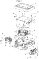
- FIG. 3 is an exploded perspective view of the controller including the semiconductor module of the electric power steering apparatus illustrated in FIG. 1 .
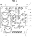
- FIG. 4 is a plan view of the semiconductor module illustrated in FIG. 3 .
- FIG. 5 is a schematic plan view of a bare-chip FET as a bare-chip transistor.
- FIG. 6 is a schematic diagram for describing a joint state between electrodes of the bare-chip FET and wiring patterns on a substrate in the semiconductor module illustrated in FIG. 3 and FIG. 4 .
- FIG. 7 is a schematic diagram for describing inclination angles between joint surfaces and surfaces to be jointed of an electrode-jointing portion and a substrate-jointing portion of a gate-electrode metal plate connector.
- a column shaft 2 of a steering wheel 1 is connected to tie rods 6 of steered wheels via a reduction gear 3, universal joints 4A and 4B, and a rack and pinion mechanism 5.
- the column shaft 2 is provided with a torque sensor 7 for detecting the steering torque of the steering wheel 1, and an electric motor 8 for outputting the assist torque that assists the steering torque of the steering wheel 1 is connected to the column shaft 2 via the reduction gear 3.
- a controller 10 that controls the electric power steering apparatus is supplied with electric power from a battery, not illustrated, and receives an ignition key signal IGN (see FIG. 2 ) via an ignition key, not illustrated.
- the controller 10 calculates a steering assist command value as an assist (steering assist) command on the basis of a steering torque Ts detected by the torque sensor 7 and a vehicle velocity V detected by a vehicle velocity sensor 9, determines a current supplied to the electric motor 8 on the basis of the calculated steering assist command value, and controls the assist torque that the electric motor 8 outputs.
- the controller 10 is mainly constituted of a microcomputer, and the mechanism and configuration of the controlling apparatus thereof are illustrated in FIG.2 .
- the steering torque Ts detected by the torque sensor 7 and the vehicle velocity V detected by the vehicle velocity sensor 9 are received by a control calculating device 11 as a control calculating unit, and a current command value calculated by the control calculating device 11 is received by a gate drive circuit 12.
- a gate drive signal formed by the gate drive circuit 12 based on the current command value and the like is received by a motor drive unit 13 including a bridge configuration of FETs.
- the motor drive unit 13 drives the electric motor 8 constituted of a three-phase brushless motor via a breaker device 14 for emergency stop.
- Each of phase currents of the three-phase brushless motor is detected by a current detecting circuit 15.
- the detected three-phase motor currents ia to ic are received by the control calculating device 11 as feedback currents.
- the three-phase brushless motor is equipped with a rotation sensor 16 such as a Hall sensor.
- a rotation signal RUT from the rotation sensor 16 is received by a rotor position detecting circuit 17 and the detected rotation position ⁇ is received by the control calculating device 11.
- the ignition key signal IGN from the ignition key is received by an ignition voltage monitoring unit 18 and a power supply circuit unit 19.
- Power-supply voltage Vdd from the power supply circuit unit 19 is received by the control calculating device 11 and a reset signal Rs for stopping the apparatus is received by the control calculating device 11.
- the breaker device 14 is constituted of relay contacts 141 and 142 for breaking two phases.
- a serial connection of FETs Tr1 and Tr2, a serial connection of FETs Tr3 and Tr4, and a serial connection of FETs Tr5 and Tr6 are connected to a power supply line 81.
- the FETs Tr1, Tr3, and Tr5 are connected in parallel to the power supply line 81, and the FETs Tr2, Tr4, and Tr6 are connected in parallel to a ground line 82.
- Such a configuration constitutes an inverter.
- the source electrode S of the FET Tr1 and the drain electrode D of the FET Tr2 are connected in series to constitute a c-phase arm of the three-phase motor, and a current is output at a c-phase output line 91c.
- the source electrode S of the FET Tr3 and the drain electrode D of the FET Tr4 are connected in series to constitute an a-phase arm of the three-phase motor, and a current is output at an a-phase output line 91a.
- the source electrode S of the FET Tr5 and the drain electrode D of the FET Tr6 are connected in series to constitute a b-phase arm of the three-phase motor, and a current is output at a b-phase output line 91b.
- FIG. 3 is an exploded perspective view of the controller 10 including the semiconductor module of the electric power steering apparatus illustrated in FIG. 1 .
- the controller 10 includes a case 20, a semiconductor module 30 as a power module including the motor drive unit 13, a heat-dissipating sheet 39, a control circuit board 40 including the control calculating device 11 and the gate drive circuit 12, a power/signal connector 50, a three-phase output connector 60, and a cover 70.
- the case 20 is formed to have a substantially rectangular shape and includes a tabular semiconductor module placement section 21 on which the semiconductor module 30 is placed, a power/signal connector mounting section 22 arranged at an end part in a length direction of the semiconductor module placement section 21 so as to mount the power/signal connector 50 thereon, and a three-phase output connector mounting section 23 arranged at an end in a width direction of the semiconductor module placement section 21 so as to mount the three-phase output connector 60 thereon.
- plural screw holes 21a into which attachment screws 38 for attaching the semiconductor module 30 are screwed are formed on the semiconductor module placement section 21.
- the semiconductor module placement section 21 and the power/signal connector mounting section 22 are provided with plural attachment posts 24 vertically standing for attaching the control circuit board 40.
- Screw holes 24a into which attachment screws 41 for attaching the control circuit board 40 are screwed are formed on the attachment posts 24, respectively.
- plural screw holes 23a into which attachment screws 61 for attaching the three-phase output connector 60 are screwed are formed on the three-phase output connector mounting section 23.
- the semiconductor module 30 has the circuit configuration of the motor drive unit 13 described above. As illustrated in FIG. 4 , the six FETs Tr1 to Tr6, a positive electrode terminal 81a connected to the power supply line 81, and a negative electrode terminal 82a connected to the ground line 82 are mounted on a substrate 31.
- a three-phase output portion 90 including an a-phase output terminal 92a connected to the a-phase output line 91a, a b-phase output terminal 92b connected to the b-phase output line 91b, and a c-phase output terminal 92c connected to the c-phase output line 91c is mounted on the substrate 31.
- Other substrate-mounted components 37 including a capacitor are mounted on the substrate 31.
- plural through-holes 31a into which attachment screws 38 for attaching the semiconductor module 30 are inserted are formed on the substrate 31 of the semiconductor module 30.
- Each of the FETUS Tr1 to Tr6 is constituted of a bare-chip FET (bare-chip transistor) 35 and includes a source electrode S and a gate electrode G on the bare-chip FET 35 as illustrated in FIG. 5 , and includes a drain electrode, not illustrated, on the lower surface of the bare-chip FET 35.
- bare-chip FET bare-chip transistor
- the gate electrode G and the source electrode S formed on the top surface of the bare-chip FET 35 are arranged straightly in series in the up-down direction in FIG. 5 , as illustrated in FIG. 5 .
- the gate electrode G has a rectangular shape having a short side extending in the up-down direction in FIG. 5 and a long side perpendicular to the short side.
- the source electrode S has a rectangular shape having a short side extending in the up-down direction in FIG. 5 and a long side perpendicular to the short side.
- the short side and the long side of the source electrode S are larger than the short side and the long side of the gate electrode G, respectively, and the area of the source electrode S is greater than the area of the gate electrode G.
- the semiconductor module 30 includes the substrate 31 made of metal, and an insulating layer 32 is formed on the substrate 31.
- the substrate 31 is made of metal such as aluminum.
- plural wiring patterns 33a to 33d are formed on the insulating layer 32.
- Each of the wiring patterns 33a to 33d is made of metal such as copper or aluminum or alloy containing these kinds of metal.
- the bare-chip FET 35 constituting each of the FETs Tr1 to Tr6 is mounted via a solder 34a on one wiring pattern 33a among the plural wiring patterns 33a to 33d.
- the drain electrode formed on the lower surface of the bare-chip FET 35 is jointed to the wiring pattern 33a via the solder 34a.
- the source electrode S of the bare-chip FET 35 and another wiring pattern 33b among the plural wiring patterns 33a to 33d are jointed together via solders 34e and 34b, respectively, by a source-electrode metal plate connector 36a.
- the gate electrode G of the bare-chip FET 35 and still another wiring pattern 33c among the plural wiring patterns 33a to 33d are jointed together via solders 34f and 34c, respectively, by a gate-electrode metal plate connector 36b.
- the other substrate-mounted component 37 such as a capacitor, is mounted via a solder 34d on a yet still another wiring pattern 33d among the plural wiring patterns 33a to 33d formed on the insulating layer 32.
- the semiconductor module 30 configured in this way is attached on the semiconductor module placement section 21 of the case 20 by the plural attachment screws 38.
- Plural through-holes 31a through which the attachment screws 38 are inserted are formed on the substrate 31 of the semiconductor module 30.
- the heat-dissipating sheet 39 is attached on the semiconductor module placement section 21, and the semiconductor module 30 is attached on the heat-dissipating sheet 39.
- the heat-dissipating sheet 39 allows the heat generated in the semiconductor module 30 to be dissipated to the case 20 via the heat-dissipating sheet 39.
- a control circuit including the control calculating device 11 and the gate drive circuit 12 is constructed by mounting plural electronic components on the control circuit board 40.
- the control circuit board 40 is attached onto the plural attachment posts 24 vertically standing on the semiconductor module placement section 21 and the power/signal connector mounting section 22 with the plural attachment screws 41 from the upper side of the semiconductor module 30.
- Plural through-holes 40a into which the attachment screws 41 are inserted are formed in the control circuit board 40.
- the power/signal connector 50 is used to supply DC power from a battery (not illustrated) to the semiconductor module 30 and to receive various signals including signals from the torque sensor 7 and the vehicle velocity sensor 9 by the control circuit board 40.
- the power/signal connector 50 is attached onto the power/signal connector mounting section 22 arranged on the semiconductor module placement section 21 with plural attachment screws 51.
- the three-phase output connector 60 is used to output currents from the a-phase output terminal 92a, the b-phase output terminal 92b, and the c-phase output terminal 92c.
- the three-phase output connector 60 is attached onto the three-phase output connector mounting section 23 arranged at an end of the semiconductor module placement section 21 in the width direction with plural attachment screws 61.
- Plural through-holes 60a into which the attachment screws 61 are inserted are formed in the three-phase output connector 60.
- cover 70 is attached onto the case 20 to which the semiconductor module 30, the control circuit board 40, the power/signal connector 50, and the three-phase output connector 60 are attached so as to cover the control circuit board 40 from the above of the control circuit board 40.
- the gate-electrode metal plate connector 36b is formed by punching and bending, that is, by press forming a metal plate composed of a material having both stiffness and high electric conductivity, such as copper (Cu), silver (Ag), gold (Au), copper alloy, and an aluminum alloy conductor.
- a metal plate composed of a material having both stiffness and high electric conductivity, such as copper (Cu), silver (Ag), gold (Au), copper alloy, and an aluminum alloy conductor.
- the gate-electrode metal plate connector 36b includes a flat plate portion 36ba, an electrode-jointing portion 36bb that is arranged on one end side of the flat plate portion 36ba in one direction (right-and-left direction in FIG. 6 and FIG.
- the substrate-jointing portion 36bc is arranged so as to be opposed to the electrode-jointing portion 36bb in the one direction (right-and-left direction in FIG. 6 and FIG.
- the electrode-jointing portion 36bb is formed to be bent from the first coupling portion 36bd and extend outward in the one direction.
- the electrode-jointing portion 36bb is formed such that a distance from the flat plate portion 36ba in a direction perpendicular to the flat plate portion 36ba (up-down direction in FIG. 6 and FIG. 7 ) is, compared to at one end (proximal end) of the electrode-jointing portion 36bb, larger at the other end (distal end).
- a joint surface (lower surface) of the electrode-jointing portion 36bb is inclined with respect to a surface to be jointed of the gate electrode G of the bare-chip FET 35, which is opposed to the joint surface (inclined downward in FIG. 6 and FIG. 7 ).
- the substrate-jointing portion 36bc is formed to be bent from the second coupling portion 36be and extend outward in the one direction.
- the substrate-jointing portion 36bc is formed such that the distance from the flat plate portion 36ba in the direction perpendicular to the flat plate portion 36ba (up-down direction in FIG. 6 and FIG. 7 ) is, compared to at one end (proximal end) of the substrate-jointing portion 36bc, larger at the other end (distal end).
- a joint surface (lower surface) of the substrate-jointing portion 36bc is inclined with respect to a surface to be jointed of the wiring pattern 33c, which is opposed to the joint surface (inclined downward in FIG. 6 and FIG. 7 ).
- An inclination angle ⁇ between the joint surface of the electrode-jointing portion 36bb and the surface to be jointed of the gate electrode G of the bare-chip FET 35 and an inclination angle ⁇ between the joint surface of the substrate-jointing portion 36bc and the surface to be jointed of the wiring pattern 33c are not particularly limited, and are preferably 0.5° or more and 7.5° or less, more preferably 2° or more and 6° or less, and particularly preferably 4°.
- the source-electrode metal plate connector 36a is formed by punching and bending, that is, by press forming a metal plate composed of a material having both stiffness and high electric conductivity, such as copper (Cu), silver (Ag), gold (Au), copper alloy, and an aluminum alloy conductor, as is the case with the gate-electrode metal plate connector 36b.
- the source-electrode metal plate connector 36a includes a flat plate portion 36aa, an electrode-jointing portion 36ab that is arranged on one end side of the flat plate portion 36aa in one direction (right-and-left direction in FIG.
- the substrate-jointing portion 36ac is arranged so as to be opposed to the electrode-jointing portion 36ab in the one direction (right-and-7-left direction in FIG. 6
- the electrode-jointing portion 36ab is formed to be bent from the first coupling portion 36ad and extend outward in the one direction.
- the electrode-jointing portion 36ab is formed such that a distance from the flat plate portion 36aa in a direction perpendicular to the flat plate portion 36aa (up-down direction in FIG. 6 ) is, compared to at one end (proximal end) of the electrode-jointing portion 36ab, larger at the other end (distal end).
- a joint surface (lower surface) of the electrode-jointing portion 36ab is inclined with respect to a surface to be jointed of the source electrode S of the bare-chip FET 35, which is opposed to the joint surface (inclined downward in FIG. 6 ).
- the substrate-jointing portion 36ac is formed to be bent from the second coupling portion 36ae and extend outward in the one direction.
- the substrate-jointing portion 36ac is formed such that the distance from the flat plate portion 36aa in the direction perpendicular to the flat plate portion 36aa (up-down direction in FIG. 6 ) is, compared to at one end (proximal end) of the substrate-jointing portion 36ac, larger at the other end (distal end).
- a joint surface (lower surface) of the substrate-jointing portion 36ac is inclined with respect to a surface to be jointed of the wiring pattern 33b, which is opposed to the joint surface (inclined downward in FIG. 6 ).
- An inclination angle ⁇ between the joint surface of the electrode--jointing portion 36ab and the surface to be jointed of the source electrode S of the bare-chip FET 35 and an inclination angle ⁇ between the joint surface of the substrate-jointing portion 36ac and the surface to be jointed of the wiring pattern 33b are not particularly limited, and are preferably 0.5 or more and 7.5° or less, more preferably 2° or more and 6° or less, and particularly preferably 4°.
- the air bubbles of the outgas generated from the molten solder move obliquely upward along the inclined joint surfaces while being combined with adjacent air bubbles, and thus are easy to be released from the solder. Furthermore, since the molten solder flows along the first coupling portions 36ad and 36bd and the second coupling portions 36ae and 36be to the lower surfaces of the flat plate portions 36aa and 36ba by a permeating and wetting phenomenon during the solder jointing (see FIG. 7 ), the air bubbles move in association with the flowing of the solder and the air bubbles are made easier to be released from the solder interposed between the joint surfaces and the surfaces to be jointed.
- the flowing of the solder to the flat plate portions 36aa and 36ba is easier to occur for the following reason. Since the temperature in the reflow furnace is higher at a higher position, in the both-electrodes metal plate connectors 36a and 36b in the reflow furnace, the flat plate portions 36aa and 36ba positioned on the upper side are higher in temperature than the electrode-jointing portions 36ab and 36bb and the substrate-jointing portions 36ac and 36bc positioned on the lower side.
- solder tends to flow from a lower-temperature region to a higher-temperature region, and thus, in the both-electrodes metal plate connectors 36a and 36b in the reflow furnace, the solder is easy to flow from the low-temperature electrode-jointing portions 36ab and 36bb and substrate-jointing portions 36ac and 36bc to the high-temperature flat plate portions 36aa and 36ba.
- the void generation rate in the solder interposed between the joint surfaces and the surfaces to be jointed is kept low, and thus the reliability of electric connection by a solder becomes high and the resistivity of the solder jointing portion becomes low. Therefore, for example, even when a high current of 100 A flows into the solder jointing portion, problems such as overheating and igniting are difficult to be generated.
- the electrode-jointing portions 36ab and 36bb are formed such that the distances from the flat plate portions 33aa and 36ba in the directions perpendicular to the flat plate portions 33aa and 36ba are, compared to at one end of the electrode-jointing portions 36ab and 36bb, smaller at the other end, and the substrate-jointing portions 36ac and 36bc are formed such that the distances from the flat plate portions 33aa and 36ba in the directions perpendicular to the flat plate portions 33aa and 36ba are, compared to at one end of the substrate-jointing portions 36ac and 36bc, smaller at the other end (in other words, the inclination direction is opposite from that in the present embodiment, and the joint surfaces are inclined upward in FIG.
- the above-described effect of making the air bubbles easier to be released by the flowing of the solder is hardly obtained.
- the molten solder hardly flows to the lower surfaces of the flat plate portions 36aa and 36ba, and thus the above-described effect of making the air bubbles easier to be released by the flowing of the solder is hardly obtained.
- the foregoing source-electrode metal plate connector 36a and gate-electrode metal plate connector 36b can be easily formed by press forming a metal plate, and thus the semiconductor module 30 of the present embodiment can be manufactured at a low cost.
- the inclination angle ⁇ is preferably 0.5° or more and 7.5° or less as described above, and when the inclination angle ⁇ is less than 0.5°, the air bubbles become difficult to be released from the solder interposed between the joint surface and the surface to be jointed. As a result, the void generation rate becomes high and the reliability of electric connection by a solder becomes insufficient, and thus, for example, when a high current of 100 A flows into the solder jointing portion, problems such as overheating and igniting may be generated.
- the joint area between the joint surface and the surface to be jointed by the solder becomes small, and thus, for example, when a high current of 100 A flows into the solder jointing portion, problems such as overheating and igniting may be generated. In addition, the strength of the solder jointing portion may become insufficient. In detail, since a distance (gap) between the joint surface and the surface to be jointed becomes large when the inclination angle ⁇ is large, the spatial volume of the gap that is to be jointed by the solder becomes large.
- the application quantity (supply quantity) of the solder to the jointing portion is fixed when the solder jointing is performed by reflow, for example, the joint area between the joint surface and the surface to be jointed by the solder becomes small. Therefore, the strength of the solder jointing portion may become insufficient.
- a minimum joint length D of the solder (length in the one direction, see FIG. 7 ) becomes small. Therefore, when the inclination angle ⁇ is more than 7.5°, a finishing state of the solder may not satisfy acceptable standards of IPC-A-610 that provides quality acceptable conditions of electronic assemblies.
- IPC-A-610 are as follows.
- L the length of each of the electrode-jointing portions 36ab and 36bb and the substrate-jointing portions 36ac and 36bc in the one direction (right-and-left direction in FIG. 7 )
- D the minimum joint length of the solder
- W the minimum width of each of the electrode-jointing portions 36ab and 36bb and the substrate-jointing portions 36ac and 36bc (length in a direction perpendicular to the one direction) is W
- FIG. 8 a result obtained by manufacturing semiconductor modules while variously changing the inclination angle ⁇ and examining the void generation rate in the solder interposed between the joint surface and the surface to be jointed is illustrated in FIG. 8 .
- 100 semiconductor modules as 1 lot were manufactured for each angle, and the void generation rates were examined for 3 lots or more of the semiconductor modules for each angle. Then, for each angle, a maximum value and a minimum value among the void generation rates of all of the semiconductor modules were plotted, and an average value of all of the void generation rates was plotted.
- the void generation rate is kept below 5% when the inclination angle ⁇ is 0.5° or more.
- the void generation rate is low, and furthermore, the variation in the void generation rate is small.
- the void generation rate rapidly becomes high, and furthermore, the variation in the void generation rate rapidly becomes large.
- the inclination angle ⁇ is preferably 7.5° or less, more preferably 6.0° or less, and further preferably 5.0° or less.
- the inclination angle ⁇ is preferably 2.5° or more, and more preferably 3.0° or more.
- the inclination angle ⁇ to be desired when manufacturing the metal plate connector (processing a metal plate)
- 4° that is the median value between the lower limit value 0.5° and the upper limit value 7.5° in the preferable range is most preferable.
- the tolerance is supposed to be plus or minus 2°
- the inclination angle ⁇ is more preferably 2° or more and 6° or less.
- the inclination angle ⁇ is preferably 0.5° or more and 7.5° or less, more preferably 2° or more and 6° or less, and further preferably 3.0° or more and 5.0° or less.
- the metal plate connectors 36a and 36b include an outgas releasing mechanism that makes the outgas generated from the molten solder during the solder jointing of the metal plate connectors 36a and 36b be released from the solders 34b, 34c, 34e, and 34f interposed between the joint surfaces and the surfaces to be jointed.
- each of the joint surfaces of the electrode-jointing portions 36ab and 36bb which are opposed to the surfaces to be jointed of the electrodes S and G of the bare-chip FET 35 and the joint surfaces of the substrate-jointing portions 36ac and 36bc which are opposed to the surfaces to be jointed of the other wiring patterns 33b and 33c is inclined with respect to each of the surfaces to be jointed, so that the outgas releasing mechanism is constituted.
- the void generation rates in the solders 34b, 34c, 34e, and 34f interposed between the joint surfaces and the surfaces to be jointed can be kept low, and thus the reliability of electric connection by a solder is high.
- the inclination angles ⁇ between the joint surfaces of the electrode-jointing portions 36ab and 36bb and the surfaces to be jointed of the electrodes S and G of the bare-chip FET 35 and the inclination angles ⁇ between the joint surfaces of the substrate-jointing portions 36ac and 36bc and the surfaces to be jointed of the wiring patterns 33b and 33c may be the same or different.
- the joint surfaces of the electrode-jointing portions 36ab and 36bb and the substrate-jointing portions 36ac and 36bc are respectively inclined with respect to the surfaces to be jointed, the contact form between the joint surfaces and the surfaces to be jointed is not surface contact but line contact. Therefore, the metal plate connectors 36a and 36b are relatively more difficult to free-stand compared to the case where the contact form between the joint surfaces and the surfaces to be jointed is surface contact.
- the metal plate connectors 36a and 36b are difficult to fall down by vibration or the like.
- the centers of gravity of the metal plate connectors 36a and 36b may be made lower by means described later (a means for providing balancing rib portions, a means for making the thicknesses of the electrode-jointing portion and the substrate-jointing portion larger than the thicknesses of other portions of the metal plate connector).
- water-repellent surface treatment may be performed on the joint surfaces of the electrode-jointing portions 36ab and 36bb and the joint surfaces of the substrate-jointing portions 36ac and 36bc.
- the wettability is improved by the surface treatment, and thus the resistivity when the air bubbles move obliquely upward along the joint surfaces becomes small, and the air bubbles become easier to be released from the solder interposed between the joint surfaces and the surfaces to be jointed.
- the type of the water-repellent surface treatment is not particularly limited, and examples thereof include tin-copper alloy plating.
- oxidation resistant treatment may be performed on the joint surfaces of the electrode-jointing portions 36ab and 36bb and the joint surfaces of the substrate-jointing portions 36ac and 36bc.
- the wettability of the solder is decreased when an oxide film is formed on the joint surface.
- an oxidation film is not formed and the wettability of the solder is high, and thus the solder is easy to flow from the electrode-jointing portions 36ab and 36bb and the substrate-jointing portions 36ac and 36bc to the flat plate portions 36aa and 36ba.
- a solder fillet can be more stably formed.
- the type of the oxidation resistant treatment is not particularly limited, and examples thereof include tin plating.
- the oxidation resistant treatment may be performed on the whole of the surface of the metal plate connectors 36a and 36b, or may be performed on only a portion with which the solder fillet to be formed comes in contact.
- the oxidation resistant treatment may be performed on the whole of the joint surfaces of the electrode-jointing portions 36ab and 36bb and the joint surfaces of the substrate-jointing portions 36ac and 36bc, the whole of the inner surfaces of the first coupling portions 36ad and 36bd and the second coupling portions 36ae and 36be, and the whole of the lower surfaces of the flat plate portions 36aa and 36ba.
- the oxidation resistant treatment may be performed on the whole of the joint surfaces of the electrode-jointing portions 36ab and 36bb and the joint surfaces of the substrate-jointing portions 36ac and 36bc, and the lower portions of the inner surfaces of the first coupling portions 36ad and 36bd and the second coupling portions 36ae and 36be (for example, to the position in the middle of the height of the metal plate connectors 36a and 36b in the up-down direction).
- the formation part of the solder fillet can be controlled because the solder fillet is difficult to be formed on the lower surfaces of the flat plate portions 36aa and 36ba.
- the oxidation resistant treatment is performed after performing masking treatment on a part of the surface of the metal plate connectors 36a and 36b, the oxidation resistant treatment can be performed on a desired part.
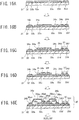
- the shapes of the source-electrode metal plate connectors 36a and the gate-electrode metal plate connector 36b may be those illustrated in FIG. 9 and FIG. 10A to FIG. 10C , for example. Since the shapes of the source-electrode metal plate connector 36a and the gate-electrcde metal plate connector 36b are substantially the same, hereinafter, only the shape of the gate-electrode metal plate connector 36b will be described later, and the description of the shape of the source-electrode metal plate connector 36a will be omitted.
- the shape of the gate-electrode metal plate connector 36b has the above-described bridge shape, and as described in more detail, the gate-electrode metal plate connector 36b includes the flat plate portion 36ba, the first coupling portion 36bd that extends downward from one end of the flat plate portion 36ba in the one direction (X-axis direction in FIG. 9 ) via a first bent portion 36bf, and the second coupling portion 36be, that extends downward from the other end of the flat plate portion 36ba in the one direction via a third bent portion 36bh to form a bridge shape (to constitute a bridge of a hat shape).
- the electrode-jointing portion 36bb is formed to be bent from the first coupling portion 36bd via a second bent portion 36bg and extend outward in the one direction
- the substrate--jointing portion 36bc is formed to be bent from the second coupling portion 36be via a fourth bent portion 36bi and extend outward in the one direction.
- the first coupling portion 36bd has a width narrow portion 36bj in the vicinity of the electrode-jointing portion 36bb.
- the width narrow portion 36bj has a tapered shape in which the width (length in Y-axis direction in FIG. 9 ) becomes narrower from the first bent portion 36bf toward the second bent portion 36bg.
- the second coupling portion 36be does not have a width narrow portion, and has a width substantially the same as that of the flat plate portion 36ba. Therefore, as illustrated in FIG. 10A to FIG. 10C , a width W1 of the electrode-jointing portion 36bb in a direction perpendicular to the one direction (Y-axis direction in FIG. 9 , and up-down direction in FIG. 10A to FIG. 10C ) is narrower than a width W2 of the substrate-jointing portion 36bc in the direction perpendicular to the one direction.
- the gate-electrode metal plate connector 36b can free-stand on the top surfaces of the bare-chip FET 35 and the substrate 31 at total three points of one point on the side of the electrode-jointing portion 36bb having a narrow width and two points (two points in the vicinity of both ends of the substrate-jointing portion 36bc in the width direction) on the side of the substrate-jointing portion 36bc having a wide width.
- the gate-electrode metal plate connector 36b can free-stand on the bare-chip FET 35 and the substrate 31 at total three points of one point on the side of the electrode-jointing portion 36bb having a narrow width and two points on the side of the substrate-jointing portion 36bc having a wide width. Accordingly, the electrode-jointing portion 36bb comes in contact with the gate electrode G of the bare-chip FET 35 at an appropriate position in spite of torsion by press forming, and the arrangement position accuracy in the solder jointing is improved. Accordingly, the jointing reliability between the electrode--jointing portion 36bb and the gate electrode G of the bare-chip FET 35 which are solder-jointed can be kept high.
- the size of the gate electrode G formed on the top surface thereof be decreased. Even if the width W1 of the electrode-jointing portion 36bb is made narrower than the width W2 of the substrate-jointing portion 36bc, when the gate electrode G formed on the bare-chip FET 35 is small, the jointing reliability causes no problem.
- the gate-electrode metal plate connector 36b fall down very easily when both the electrode-jointing portion 36bb and the substrate-jointing portion 36bc are made to have narrow widths in the gate-electrode metal plate connector 36b, and the gate-electrode metal plate connector 36b is made to free-stand on the bare-chip FET 35 and the substrate 31 at total two points of one point on the side of the electrode-jointing portion 36bb having a narrow width and one point on the side of the substrate-jointing portion 36bc having a narrow width.
- the electrode-jointing portion 36bb in the gate-electrode metal plate connector 36b is located substantially at the center of the substrate-jointing portion 36bc in the width direction perpendicular to the one direction. Accordingly, the electrode-jointing portion 36bb having a narrow width is located at a position well balanced with respect to the width direction of the substrate-jointing portion 36bc.
- the gate-electrode metal plate connector 36b free-stands on the bare-chip FET 35 and the substrate 31 at total three points of one point on the side of the electrode-jointing portion 36bb having a narrow width and two points on the side of the substrate-jointing portion 36bc having a wide width, the free-standing ability of the gate-electrode metal plate connector 36b can be improved by the good balance in positioning of the electrode-jointing portion 36bb.
- the center of gravity of the gate-electrode metal plate connector 36b may be made lower by providing balancing rib portions 36bl for the gate-electrode metal plate connector 36b, or making the thicknesses of the electrode-jointing portion 36bb and the substrate-jointing portion 36bc larger than the thicknesses of other portions of the metal plate connector.
- the balancing rib portions 36bl will be described.
- the gate-electrode metal plate connector 36b as illustrated in FIG. 11A , at both ends of the flat plate portion 36ba in the direction perpendicular to the one direction, which is provided between the electrode-jointing portion 36bb and the substrate-jointing portion 36bc, the balancing rib portions 36bl and 36bl may be respectively formed to be bent down from the both ends.
- the position of the center of gravity of the gate-electrode metal plate connector 36b is lowered by the balancing rib portions 36bl, and the free-standing ability of the gate-electrode metal plate connector 36b is improved.
- the gate-electrode metal plate connector 36b free-stands on the top surfaces of the bare-chip transistor and the substrate at total three points of one point on the side of the electrode-jointing portion 36bb having a narrow width and two points on the side of the substrate-jointing portion 36bc having a wide width, the free-standing ability is stably improved.
- the plate thicknesses of the electrode-jointing portion 36bb and the substrate-jointing portion 36bc of the gate-electrode metal plate connector 36b may be lager than the plate thicknesses of the other portions (that is, the flat plate portion 36ba, the first coupling portion 36bd, and the second coupling portion 36be) of the gate-electrode metal plate connector 36b.
- the size of the plate thicknesses of the electrode-jointing portion 36bb and the substrate-jointing portion 36bc may be, but not particularly limited to, for example, about three times (3L) the plate thicknesses L of the other portions (that is, the flat plate portion 36ba, the first coupling portion 36bd, and the second coupling portion 36be) of the gate-electrode metal plate connector 36b.
- the plate thicknesses of the electrode-jointing portion 36bb and the substrate-jointing portion 36bc are large, the position of the center of gravity of the gate-electrode metal plate connector 36b is lowered, and the free-standing ability is improved.
- the gate-electrode metal plate connector 36b free-stands on the top surfaces of the bare-chip transistor and the substrate at total three points of one point on the side of the electrode-jointing portion 36bb having a narrow width and two points on the side of the substrate-jointing portion 36bc having a wide width, the free-standing ability is stably improved.
- a stress-reducing portion is arranged between the electrode-jointing portion 36bb and the substrate-jointing portion 36bc.
- the stress-reducing portion is constituted of a bridge shape including the flat plate portion 36ba, the first coupling portion 36bd bent down from one end of the flat plate portion 36ba via the first bent portion 36bf, and the second coupling portion 36be bent down from the other end of the flat plate portion 35ba via the third bent portion 36bh.
- the gate-electrode metal plate connector 36b is made into a bridge shape such that the respective sides of the bridge shape (the flat plate portion 36ba, the first coupling portion 36bd, and the second coupling portion 36be) not only expand and contract, but also are deformable in a direction in which the respective bent portions 36bf, 36bg, 36bh, and 36bi are bending.
- the effect of a plate spring is obtained, and displacement in the up-down and right-and-left directions (Z-axis direction and X-axis direction in FIG. 9 ) is absorbable by virtue of a bridge shape framework. That is, in a case where deformation of the substrate 31 and the metal plate connectors 36a and 36b occurs due to thermal expansion or thermal contraction, the metal plate connectors 36a and 36b can be easily bent.
- the substrate 31 is made of aluminum, the linear expansion coefficient thereof is about 23.6 x 10 -6 /°C, and the linear expansion coefficient of the gate-electrode metal plate connector 36b made of a copper plate is about 16.8 x 10 -6 /°C.
- the bare-chip FET is made of silicon and the linear expansion coefficient thereof is about 2.5 x 10 -6 /°C.
- the stress-reducing portion when the stress-reducing portion is arranged between the electrode-jointing portion 36bb and the substrate-jointing portion 36bc, the stress-reducing portion is generally formed in a wavelike shape (a bridge shape in the present embodiment) and thus the gate-electrode metal plate connector 36b has a shape having difficulty in free-standing.
- the gate-electrode metal plate connector 36b can free-stand on the bare-chip FET 35 and the substrate 31 at total three points of one point on the side of the electrode-jointing portion 36bb having a narrow width and two points on the side of the substrate-jointing portion 36bc having a wide width, and thus the free-standing ability of the gate-electrode metal plate connector 36b is ensured.
- the first coupling portion 36bd in the gate-electrode metal plate connector 36b is formed to have a tapered shape in which the width gradually decreases from the flat plate portion 36ba to the electrode-jointing portion 36bb as illustrated in FIG. 10A to FIG. 10C , and a bending baseline of the electrode-jointing portion 36bb, that is, a baseline of the second bent portion 36bg is the narrowest portion of the first coupling portion 36bd.
- the electrode-jointing portion 36bb can be easily deformed at the bending baseline. Accordingly, when the gate-electrode metal plate connector 36b is deformed in the solder jointing or the like due to the difference in linear expansion coefficient between the bare-chip FET 35 and the gate-electrode metal plate connector 36b, the difference in linear expansion coefficient between the substrate 31 and the gate-electrode metal plate connector 36b, and the difference in linear expansion coefficient between the bare-chip FET 35 and the substrate 31, the electrode-jointing portion 36bb can be easily deformed at the bending baseline. As a result, it is possible to ensure the jointing reliability of the electrode-jointing portion 36bb to the gate electrode G.
- progressive cut portions 36bk formed by a progressive press in press forming are provided at both ends of the flat plate portion 36ba in the width direction (Y-axis direction in FIG. 9 , and up-down direction in FIG. 10A to FIG. 10C ).
- the progressive cut portions 36bk are formed to protrude outward in the width direction of the flat plate portion 36ba.
- the progressive cut portions 36bk are arranged at a flat surface (flat plate portion 36ba) of the gate-electrode metal plate connector 36b, cutting is easily performed and deformation of components in a cutting process can be suppressed. Furthermore, since the progressive cut portions 36bk are formed to protrude outward from the flat plate portion 36ba, cutting can be performed without deforming the flat surface of the flat plate portion 36ba.
- the gate-electrode metal plate connector 36b includes the four bent portions (36bf, 36bg, 36bh, 36bi) and has a bridge shape.
- the angle of each of the bent portions (36bf, 36bg, 36bh, 36bi) may be an obtuse angle (for example, 95°, 99°) as an example illustrated in FIG. 13 .
- the gate-electrode metal plate connector 36b can be more suitably manufactured using press forming.
- angles of the four bent portions are obtuse angles
- the mold releasability during press forming can be improved, which contributes to reduction in manufacturing costs.
- a stress acts on the gate-electrode metal plate connector 36b inward in the one direction of the flat plate portion 36ba, and thus the gate-electrode metal plate connector 36b can be placed in a stable state.
- the center of gravity C can be provided at the flat surface (flat plate portion 36ba) of a substantially middle portion of the gate-electrode metal plate connector 36b by making the gate-electrode metal plate connector 36b be the bridge shape (see FIG. 9 ). Therefore, when the gate-electrode metal plate connector 36b is suctioned and held by a transfer jig in loading to the substrate 31, the center of gravity C located at this flat surface can be suctioned.
- the suction range of the position of the center of gravity in the flat plate portion ba of the gate-electrode metal plate connector 36b is preferably an area of about 2 mm 2 , and more preferably an area of about 2 to 5 mm 2 .
- the thickness of the flat plate portion 36ba is preferably larger than the thicknesses of the other portions of the gate-electrode metal plate connector 36b, that is, the electrode-jointing portion 36bb, the substrate-jointing portion 36bc, the first coupling portion 36bd, and the second coupling portion 36be.
- the size of the plate thickness of the flat plate portion 36ba may be, but not particularly limited to, for example, about three times (3L) the plate thicknesses L of the other portions of the gate-electrode metal plate connector 36b, that is, the electrode-jointing portion 36bb, the substrate-jointing portion 36bc, the first coupling portion 36bd, and the second coupling portion 36be.
- the gate-electrode metal plate connector 36b may have any shape as long as it has the bridge shape capable of jointing the gate electrode G to the wiring pattern 33c.
- the gate-electrode metal plate connector 36b may have a shape in which no width narrow portion 36bj is provided.
- the gate-electrode metal plate connector 36b may have a shape in which the widths of the first coupling portion 36bd, the electrode-jointing portion 36bb, the second coupling portion 36be, and the substrate-jointing portion 36bc are substantially the same as the width of the flat plate portion 36ba.
- the balancing rib portions 36bl may be provided so as to improve the free-standing ability of the gate-electrode metal plate connector 36b (see FIG. 11B ), as is the case with the gate-electrode metal plate connector 36b having the shape illustrated in FIG. 9 .
- the thicknesses of the electrode-jointing portion 36bb and the substrate-jointing portion 36bc may be larger than the thicknesses of the other portions of the metal plate connector (see FIG. 12B ).
- the thickness of the flat plate portion 36ba may be larger than the thicknesses of the other portions of the gate-electrode metal plate connector 36b (see FIG. 14B ).
- the insulating layer 32 is formed on one main surface of the substrate 31 made of metal (insulating layer forming step).
- the plural wiring patterns 33a to 33d are formed on the insulating layer 32 (wiring pattern forming step).
- solder pastes (the solders 34a to 34d) are applied on the plural wiring patterns 33a to 33d, respectively (solder paste applying step).
- one bare-chip FET 35 is mounted on the solder paste (the solder 34a) applied onto one wiring pattern 33a among the plural wiring patterns 33a to 33d (bare-chip FET mounting step), and the other substrate-mounted component 37 is mounted on the solder paste (the solder 34d) applied onto another wiring pattern 33d.
- Another bare-chip FET 35 is also mounted on a wiring pattern identical to or different from the wiring pattern 33a.
- solder pastes (the solders 34e and 34f) are applied onto the source electrode S and the gate electrode G formed on the top surface of the bare-chip FET 35 (solder paste applying step).
- the source-eleccrode metal plate connector 36a is mounted on the solder paste (the solder 34e) applied onto the source electrode S of the bare-chip FET 35 and the solder paste (the solder 34b) applied onto another wiring pattern 33b other than the wiring pattern 33a on which the bare-chip FET 35 is mounted, among the plural wiring patterns 33a to 33d (source-electrode metal plate connector mounting step).
- the gate-electrode metal plate connector 36b is mounted on the solder paste (the solder 34f) applied onto the gate electrode G of the bare-chip FET 35 and the solder paste (the solder 34c) applied onto still another wiring pattern 33c other than the wiring pattern 33a on which the bare-chip FET 35 is mounted and other than the wiring pattern 33b on which the source-electrode metal plate connector 36a is mounted, among the plural wiring patterns 33a to 33d (gate-electrode metal plate connector mounting step).
- An intermediate semiconductor module assembly is constructed in this way.
- the intermediate semiconductor module assembly constructed through the steps described above is put into a reflow furnace (not illustrated), and the jointing between one wiring pattern 33a among the plural wiring patterns 33a to 33d and the bare-chip FET 35 via the solder 34a, the jointing between the wiring pattern 33d and the other substrate-mounted component 37 via the solder 34d, the jointing between the source electrode S formed on the top surface of the bare-chip FET 35 and the source-electrode metal plate connector 36a via the solder 34e, the jointing between another wiring pattern 33b among the plural wiring patterns 33a to 33d and the source-electrode metal plate connector 36a, the jointing between the gate electrode G formed on the top surface of the bare-chip FET 35 and the gate-electrode metal plate connector 36b via the solder 34f, and the jointing between still another wiring pattern 33c among the plural wiring patterns 33a to 33d and the gate-electrode metal plate connector 36b via the solder 34c are collectively carried out (jointing step).
- the source electrode S of the bare-chip FET 35 and the wiring pattern 33b on the substrate 31, and the gate electrode G of the bare-chip FET 35 and another wiring pattern 33c on the substrate 31 can be jointed by the solder mounting operation using the source-electrode metal plate connector 36a and the gate-electrode metal plate connector 36b, it is possible to carry out the jointing between the source electrode S of the bare-chip FET 35 and the wiring pattern 33b on the substrate 31 and the jointing between the gate electrode G of the bare-chip FET 35 and another wiring pattern 33c on the substrate 31, simultaneously in the same apparatus and in the same process as the solder mounting operation for mounting the bare-chip FET 35 or the other substrate-mounted component 37 on the wiring patterns 33a and 33d on the substrate 31. As a result, it is possible to shorten the manufacturing tact time of the semiconductor module 30, to make a dedicated wire bonding apparatus unnecessary, and to reduce the manufacturing costs of the semiconductor module 30.
- the width W1 of the electrode-jointing portion 36bb in the direction perpendicular to the one direction is narrower than the width W2 of the substrate-jointing portion 36bc in the direction perpendicular to the one direction in the gate-electrode metal plate connector 36b, and the gate-electrode metal plate connector 36b can free-stand on the top surfaces of the bare-chip FET 35 and the substrate 31 at total three points of one point on the side of the electrode-jointing portion 36bb having a narrow width and two points (two points in the vicinity of both ends of the substrate-jointing portion 36bc in the width direction) on the side of the substrate-jointing portion 36bc having a wide width.
- the substrate 31 of the semiconductor module 30 is made of aluminum, and the source-electrode metal plate connector 36a and the gate-electrode metal plate connector 36b are made of a metal material having both stiffness and high electric conductivity.
- the linear expansion coefficient of aluminum is 23.6 x 10 -6 /°C, and the linear expansion coefficient of the copper material is 16.8 x 10 -6 /°C as an example. That is, the substrate 31 is more easily deformed by a temperature change than the source-electrode metal plate connector 36a and the gate-electrode metal plate connector 36b.
- the metal plate connectors 36a and 36b are made into a bridge shape such that the respective sides of the bridge shape (the flat plate portions 36aa and 36ba, the first coupling portions 36ad and 36bd, and the second coupling portions 36ae and 36be) not only expand and contract, but also are deformable in a direction in which the respective bent portions are bending.
- the effect of a plate spring is obtained, and displacement in the up-down and right-and-left directions (Z-axis direction and X-axis direction in FIG. 9 ) is absorbable by virtue of a bridge shape framework. That is, in a case where deformation of the substrate 31 and the metal plate connectors 36a and 36b occurs due to thermal expansion or thermal contraction, the metal plate connectors 36a and 36b can be easily bent.
- the metal plate connectors 36a and 36b can appropriately absorb displacement when being deformed in the reflow process and when being deformed due to heat generation during the EPS operation, it is possible to prevent the solder jointing between the metal plate connectors 36a and 36b and the bare-chip FET 35 from separating, and to secure the reliability of electric connection.
- the bare-chip FET 35 is used in the semiconductor module 30, not only the bare-chip FET 35 but also other bare-chip transistors, such as a bare-chip IGBT, may be used.
- an electrode formed on the top surface of the bare-chip transistor and another wiring pattern other than a wiring pattern to which the bare-chip transistor is jointed, among plural wiring patterns, may be jointed via solders by a metal plate connector. Accordingly, the jointing between the electrode of the bare-chip transistor and the wiring pattern on the substrate can be performed simultaneously in the same apparatus and in the same process as the solder mounting operation for mounting the bare-chip transistor or other substrate-mounted components on the wiring patterns on tne substrate.
- an emitter electrode and a gate electrode formed on the bare-chip IGBT be jointed to wiring patterns on the substrate, respectively, via solders using a metal plate connector.
- the jointing between the emitter electrode of the bare-chip IGBT and a wiring pattern on the substrate and the jointing between the gate electrode of the bare-chip IGBT and another wiring pattern on the substrate can be performed simultaneously in the same apparatus and in the same process as the solder mounting operation for mounting the bare-chip IGBT or other substrate-mounted components on the wiring patterns on the substrate.
- a stress-reducing portion having another constitution may be further provided.
- a stress-reducing portion constituted by forming a notch portion 36bm in the electrode-jointing portions 36ab and 36bb and the substrate-jointing portions 36ac and 36bc see FIG. 17
- a stress-reducing portion constituted by forming chamfered portions 36bn (the chamfered portions may be C chamfering in place of R chamfering illustrated in the drawing) at the corners of the end portion of the electrode-jointing portions 36ab and 36bb and the substrate-jointing portions 36ac and 36bc (see FIG.
- a symbol P in FIG. 17 to FIG. 20 indicates a source PAD.
- a stress in a twist direction can be reduced.
- the stress-reducing portion constituted by forming the notch portion 36bm contact points between the electrode-jointing portions 36ab and 36bb and the bare-chip FET 35, or contact points between the substrate-jointing portions 36ac and 36bc and the wiring patterns 33b and 33c become two, and the width of each of the contact portions becomes narrow, and thus, even when being twisted by thermal deformation, the electrode-jointing portions 36ab and 36bb and the substrate-jointing portions 36ac and 36bc are easy to conform with the twist.
- the contact points become two, that is, a dual system can be constituted, the reliability of electric connection is improved.
- the stress-reducing portion constituted by making the thicknesses of the electrode-jointing portions 36ab and 36bb and the substrate-jointing portions 36ac and 36bc smaller than the thicknesses of the other portions of the metal plate connectors 36a and 36b
- the plate thicknesses of the electrode-jointing portions 36ab and 36bb and the substrate-jointing portions 36ac and 36bc are thin, and thus are easy to be twisted and to absorb displacement in thermal deformation.
- the stress-reducing portion constituted by forming the chamfered portions 36bn at the corners of the end portion of the electrode-jointing portions 36ab and 36bb and the substrate-jointing portions 36ac and 36bc is provided, the effect that, when the electrode-jointing portions 36ab and 36bb and the substrate-jointing portions 36ac and 36bc are twisted by thermal deformation, stress concentration on the corners is made to escape is obtained.
- the stress-reducing portion constituted by forming the hole 36bp at the center of the electrode-jointing portions 36ab and 36bb and the substrate-jointing portions 36ac and 36bc is provided, even when being twisted by thermal deformation, the electrode-jointing portions 36ab and 36bb and the substrate-jointing portions 36ac and 36bc are easy to conform with the twist.
- solder flows to the top surfaces of the electrode-jointing portions 36ab and 36bb and the substrate-jointing portions 36ac and 36bc to radiate by the permeating and wetting phenomenon, the solder is difficult to be separated when the electrode-jointing portions 36ab and 36bb and the substrate-jointing portions 36ac and 36bc are twisted.
- the gate-electrode metal plate connector may have one type and the source-electrode metal plate connector may have two types.
- the source-electrode metal plate connector has two types including a first source-electrode metal plate connector (see Tr2 and Tr4 in FIG. 4 ) arranged 180 degrees straightly with respect to the gate-electrode metal plate connector and a second source-electrode metal plate connector (see Tr1, Tr3, and Tr5 in FIG. 4 ) arranged 90 degrees perpendicularly with respect to the gate-electrode metal plate connector.
- the one type of gate-electrode metal plate connector and any source-electrode metal plate connector selected from two types of the first source-electrode metal plate connector and the second source-electrode metal plate connector can be used in combination for one bare-chip FET.
- the arrangement (the angle between the gate-electrode metal plate connector and the first source-electrode metal plate connector, i.e. the angle between the one direction of the gate-electrode metal plate connector and the one direction of the first source-electrode metal plate connector) of the first source-electrode metal plate connector with respect to the gate-electrode metal plate connector preferably ranges from 95 degrees to 265 degrees, more preferably ranges from 160 degrees to 200 degrees, still more preferably ranges from 175 degrees to 185 degrees, and is most preferably set to 180 degrees.
- the arrangement (the angle between the gate-electrode metal plate connector and the second source-electrode metal plate connector, i.e. the angle between the one direction of the gate-electrode metal plate connector and the one direction of the second source-electrode metal plate connector) of the second source-electrode metal plate connector with respect to the gate-electrode metal plate connector preferably ranges from 5 degrees to 175 degrees, more preferably ranges from 70 degrees to 120 degrees, still more preferably ranges from 85 degrees to 95 degrees, and is most preferably set to 90 degrees.
- a degree of freedom in arranging the bare-chip transistor mounted on the substrate increases, a degree of freedom in design of wirings on the substrate increases, and thus the layout of the semiconductor module on the substrate can be made to be compact. It is possible to easily make the path lengths for phases of a three-phase motor on the substrate identical. Accordingly, it is possible to make characteristics of the phases of the three-phase motor, particularly, the impedance characteristics of the phases, easily match each other, thereby improving ripple accuracy of torque, velocity, and so on.
Landscapes
- Power Steering Mechanism (AREA)
- Cooling Or The Like Of Semiconductors Or Solid State Devices (AREA)
- Structures For Mounting Electric Components On Printed Circuit Boards (AREA)
- Physics & Mathematics (AREA)
- Geometry (AREA)
- Chemical & Material Sciences (AREA)
- Engineering & Computer Science (AREA)
- Ceramic Engineering (AREA)
Abstract
Description
- The present invention relates to a semiconductor module such as a power module incorporated into automotive electrical equipment.
- In recent years, electronic devices have been introduced for controlling various electrical equipment in a vehicle such as an automobile. In an electric power steering apparatus as an example of electrical equipment into which an electronic device is incorporated, there is provided a motor drive unit in an enclosure accommodating an electric motor for steering an automobile and the electronic device is mounted on the motor drive unit. The electronic device is incorporated as a power module into the motor drive unit.
- The power module is constituted as a so-called semiconductor module on which a power element such as a field effect transistor (FET) or an insulated gate bipolar transistor (IGBT) suitable for controlling electrical equipment driven with a relatively large current, such as an electric power steering apparatus, is mounted. Such a type of power module is also called "in-vehicle module", because it is mounted on a vehicle.
- A power element is mounted on a substrate by solder jointing when manufacturing such a semiconductor module, and a technique for electrically connecting a semiconductor chip and a lead frame using an arch-shaped metal piece is disclosed in
PTL -
- PTL 1:
JP 2011-243752 A - PTL 2:
JP 2012-212712 A - PTL 3:
JP 2006-114571 A - However, in the technique disclosed in
PTL - In a surface-mounting semiconductor device such as a thin quad flat package (TQFP), a technique for making it easy for outgas generated from a molten solder to be released from the solder during solder jointing of a lead for an external connection of the semiconductor device is disclosed in
PTL 3. In other words, since tapered portions are provided on four surfaces (top surface, lower surface, and both side surfaces) of a lead tip such that the tip is tapered, air bubbles of the outgas generated from the molten solder during the solder jointing move toward the lead tip along the tapered portion on the lower surface while being combined with adjacent air bubbles on the tapered portion on the lower surface of the lead, and are released from the solder. - In addition, since the molten solder is easy to be wetted and spread along not only the tapered portion on the lower surface but also the tapered portions on the side surfaces of the lead and the surface of the side surfaces of the lead, and furthermore, is easy to be wetted and spread also on the tapered portion on the top surface of the lead, the solder is jointed to the whole of the four surfaces of the lead tip. As a result, the joint area becomes large, and the reliability of electric connection by a solder becomes high.
- However, in the technique disclosed in
PTL 3, since the tapered portions need to be provided by processing the four surfaces of the lead tip, there was a problem in that the manufacturing costs are increased. - Thus, an object of the present invention is to solve the above-described problems of the conventional arts and to provide a semiconductor module that has high reliability of electric connection by a solder and is inexpensive.
- In order to solve the above-described problems, according to one embodiment of the present invention, there is provided a semiconductor module including: a substrate made of metal; an insulating layer formed on the substrate; a plurality of wiring patterns formed on the insulating layer; a bare-chip transistor mounted on one wiring pattern among the plurality of wiring patterns via a solder; and a metal plate connector formed of a metal plate, the metal plate connector jointing an electrode formed on a top surface of the bare-chip transistor and another wiring pattern among the plurality of wiring patterns.
- The metal plate connector includes a flat plate portion, an electrode-jointing portion that is arranged on one end side of the flat plate portion in one direction and is jointed to the electrode of the bare-chip transistor via a solder, a substrate-jointing portion that is arranged on the other end side of the flat plate portion in the one direction and is jointed to the another wiring pattern via a solder, a first coupling portion that extends downward from the one end of the flat plate portion in the one direction and couples the one end of the flat plate portion in the one direction to one end of the electrode-jointing portion, and a second coupling portion that extends downward from the other end of the flat plate portion in the one direction and couples the other end of the flat plate portion in the one direction to one end of the substrate-jointing portion to form a bridge shape.
- In addition, the electrode-jointing portion is formed to be bent from the first coupling portion and extend outward in the one direction and the substrate-jointing portion is formed to be bent from the second coupling portion and extend outward in the one direction.
- Then, a joint surface of the electrode-jointing portion that is opposed to a surface to be jointed of the electrode of the bare-chip transistor and a joint surface of the substrate-jointing portion that is opposed to a surface to be jointed of the another wiring pattern include an outgas releasing mechanism that makes outgas generated from a molten solder during solder jointing of the metal plate connector be released from the solders interposed between the joint surfaces and the surfaces to be jointed.
- In addition, according to another embodiment of the present invention, there is provided a semiconductor module including: a substrate made of metal; an insulating layer formed on the substrate; a plurality of wiring patterns formed on the insulating layer; a bare-chip transistor mounted on one wiring pattern among the plurality of wiring patterns via a solder; and a metal plate connector formed of a metal plate, the metal plate connector jointing an electrode formed on a top surface of the bare-chip transistor and another wiring pattern among the plurality of wiring patterns.
- The metal plate connector includes a flat plate portion, an electrode-jointing portion that is arranged on one end side of the flat plate portion in one direction and is jointed to the electrode of the bare-chip transistor via a solder, a substrate-jointing portion that is arranged on the other end side of the flat plate portion in the one direction and is jointed to the another wiring pattern via a solder, a first coupling portion that extends downward from the one end of the flat plate portion in the one direction and couples the one end of the flat plate portion in the one direction to one end of the electrode-jointing portion, and a second coupling portion that extends downward from the other end of the flat plate portion in the one direction and couples the other end of the flat plate portion in the one direction to one end of the substrate-jointing portion to form a bridge shape.
- In addition, the electrode-jointing portion is formed to be bent from the first coupling portion and extend outward in the one direction, and is formed such that a distance from the flat plate portion in a direction perpendicular to the flat plate portion is, compared to at the one end of the electrode--jointing portion, larger at the other end, such that a joint surface of the electrode-jointing portion is inclined with respect to a surface to be jointed of the electrode of the bare-chip transistor, which is opposed to the joint surface.
- Furthermore, the substrate-jointing portion is formed to be bent from the second coupling portion and extend outward in the one direction, and is formed such that the distance from the flat plate portion in the direction perpendicular to the flat plate portion is, compared to at the one end of the substrate-jointing portion, larger at the other end, such that a joint surface of the substrate-jointing portion is inclined with respect to a surface to be jointed of the another wiring pattern, which is opposed to the joint surface.
- In the semiconductor module according to the another embodiment, an inclination angle between the joint surface of the electrode-jointing portion and the surface to be jointed of the electrode of the bare-chip transistor and an inclination angle between the joint surface of the substrate-jointing portion and the surface to be jointed of the another wiring pattern may be 0.5° or more and 7.5° or less.
- In addition, in the semiconductor module according to the one embodiment and the semiconductor module according to the another embodiment, a width of the electrode-jointing portion in a direction perpendicular to the one direction may be narrower than a width of the substrate-jointing portion in the direction perpendicular to the one direction.
- Furthermore, in the semiconductor module according to the one embodiment and the semiconductor module according to the another embodiment, at both ends of the flat plate portion in a direction perpendicular to the one direction, balancing rib portions may be respectively formed to be bent down from the both ends.
- Furthermore, in the semiconductor module according to the one embodiment and the semiconductor module according to the another embodiment, thicknesses of the electrode-jointing portion and the substrate-jointing portion may be larger than a thickness of another portion of the metal plate connector.
- Furthermore, in the semiconductor module according to the one embodiment and the semiconductor module according to the another embodiment, wherein a thickness of the flat plate portion may be larger than a thickness of another portion of the metal plate connector.
- According to embodiments of the present invention, there is provided a semiconductor module that has high reliability of electric connection by a solder and is inexpensive.
-
-
FIG. 1 is a diagram illustrating a basic structure of an electric power steering apparatus employing a semiconductor module according to one embodiment of the present invention; -
FIG. 2 is a block diagram illustrating a control system of a controller of the electric power steering apparatus illustrated inFIG. 1 ; -
FIG. 3 is an exploded perspective view of the controller including the semiconductor module of the electric power steering apparatus illustrated inFIG. 1 ; -
FIG. 4 is a plan view of the semiconductor module illustrated inFIG. 3 ; -
FIG. 5 is a schematic plan view of a bare-chip FET as a bare-chip transistor; -
FIG. 6 is a schematic diagram for describing a joint state between electrodes of the bare-chip FET and wiring patterns on a substrate in the semiconductor module illustrated inFIG. 3 andFIG. 4 ; -
FIG. 7 is a schematic diagram describing inclination angles between joint surfaces and surfaces to be jointed of an electrode--jointing portion and a substrate-jointing portion of a metal plate connector; -
FIG. 8 is a graph illustrating a relationship between the inclination angle and the void generation rate; -
FIG. 9 is a perspective view illustrating an example of the shape of the metal plate connector; -
FIG. 10A is a plan view of the metal plate connector ofFIG. 9 ; -
FIG. 10B is a front view of the metal plate connector ofFIG. 9 ; -
FIG. 10C is a rear view of the metal plate connector ofFIG. 9 ; -
FIG. 11A and FIG. 11B are perspective views illustrating the metal plate connector having balancing rib portions; -
FIG. 12A and FIG. 12B are perspective views illustrating the metal plate connector in which the electrode-jointing portion and the substrate-jointing portion have large thicknesses; -
FIG. 13 is a side view illustrating the shape of the metal plate connector ofFIG. 9 andFIG. 10A to FIG. 10C ; -
FIG. 14A and FIG. 14B are perspective views illustrating the metal plate connector in which a flat plate portion has a large thickness; -
FIG. 15 is a perspective view illustrating another example of the shape of the metal plate connector; -
FIG. 16A to FIG. 16E are diagrams for describing a manufacturing process of the semiconductor module; -
FIG. 17 is a diagram illustrating an example of a stress-reducing portion; -
FIG. 18 is a diagram illustrating another example of the stress-reducing portion; -
FIG. 19 is a diagram illustrating another example of the stress-reducing portion; and -
FIG. 20 is a diagram illustrating another example of the stress-reducing portion. - Embodiments of the present invention will be described in detail with reference to the drawings.
FIG. 1 is a diagram illustrating a basic structure of an electric power steering apparatus employing a semiconductor module according to one embodiment of the present invention.FIG. 2 is a block diagram illustrating a control system of a controller of the electric power steering apparatus illustrated inFIG. 1 .FIG. 3 is an exploded perspective view of the controller including the semiconductor module of the electric power steering apparatus illustrated inFIG. 1 .FIG. 4 is a plan view of the semiconductor module illustrated inFIG. 3 . -
FIG. 5 is a schematic plan view of a bare-chip FET as a bare-chip transistor.FIG. 6 is a schematic diagram for describing a joint state between electrodes of the bare-chip FET and wiring patterns on a substrate in the semiconductor module illustrated inFIG. 3 andFIG. 4 .FIG. 7 is a schematic diagram for describing inclination angles between joint surfaces and surfaces to be jointed of an electrode-jointing portion and a substrate-jointing portion of a gate-electrode metal plate connector. - In the electric power steering apparatus of
FIG. 1 , acolumn shaft 2 of asteering wheel 1 is connected to tie rods 6 of steered wheels via areduction gear 3,universal joints pinion mechanism 5. Thecolumn shaft 2 is provided with atorque sensor 7 for detecting the steering torque of thesteering wheel 1, and anelectric motor 8 for outputting the assist torque that assists the steering torque of thesteering wheel 1 is connected to thecolumn shaft 2 via thereduction gear 3. - A
controller 10 that controls the electric power steering apparatus is supplied with electric power from a battery, not illustrated, and receives an ignition key signal IGN (seeFIG. 2 ) via an ignition key, not illustrated. Thecontroller 10 calculates a steering assist command value as an assist (steering assist) command on the basis of a steering torque Ts detected by thetorque sensor 7 and a vehicle velocity V detected by avehicle velocity sensor 9, determines a current supplied to theelectric motor 8 on the basis of the calculated steering assist command value, and controls the assist torque that theelectric motor 8 outputs. - The
controller 10 is mainly constituted of a microcomputer, and the mechanism and configuration of the controlling apparatus thereof are illustrated inFIG.2 . - The steering torque Ts detected by the
torque sensor 7 and the vehicle velocity V detected by thevehicle velocity sensor 9 are received by acontrol calculating device 11 as a control calculating unit, and a current command value calculated by thecontrol calculating device 11 is received by agate drive circuit 12. A gate drive signal formed by thegate drive circuit 12 based on the current command value and the like is received by amotor drive unit 13 including a bridge configuration of FETs. Themotor drive unit 13 drives theelectric motor 8 constituted of a three-phase brushless motor via abreaker device 14 for emergency stop. - Each of phase currents of the three-phase brushless motor is detected by a current detecting
circuit 15. The detected three-phase motor currents ia to ic are received by thecontrol calculating device 11 as feedback currents. In addition, the three-phase brushless motor is equipped with arotation sensor 16 such as a Hall sensor. A rotation signal RUT from therotation sensor 16 is received by a rotorposition detecting circuit 17 and the detected rotation position θ is received by thecontrol calculating device 11. - Additionally, the ignition key signal IGN from the ignition key is received by an ignition
voltage monitoring unit 18 and a powersupply circuit unit 19. Power-supply voltage Vdd from the powersupply circuit unit 19 is received by thecontrol calculating device 11 and a reset signal Rs for stopping the apparatus is received by thecontrol calculating device 11. Thebreaker device 14 is constituted ofrelay contacts 141 and 142 for breaking two phases. - Additionally, the circuit configuration of the
motor drive unit 13 will be described later. A serial connection of FETs Tr1 and Tr2, a serial connection of FETs Tr3 and Tr4, and a serial connection of FETs Tr5 and Tr6 are connected to apower supply line 81. The FETs Tr1, Tr3, and Tr5 are connected in parallel to thepower supply line 81, and the FETs Tr2, Tr4, and Tr6 are connected in parallel to aground line 82. Such a configuration constitutes an inverter. - In such a configuration, in the FETs Tr1 and Tr2, the source electrode S of the FET Tr1 and the drain electrode D of the FET Tr2 are connected in series to constitute a c-phase arm of the three-phase motor, and a current is output at a c-
phase output line 91c. In the FETs Tr3 and Tr4, the source electrode S of the FET Tr3 and the drain electrode D of the FET Tr4 are connected in series to constitute an a-phase arm of the three-phase motor, and a current is output at ana-phase output line 91a. In the FETs Tr5 and Tr6, the source electrode S of the FET Tr5 and the drain electrode D of the FET Tr6 are connected in series to constitute a b-phase arm of the three-phase motor, and a current is output at a b-phase output line 91b. - Next,
FIG. 3 is an exploded perspective view of thecontroller 10 including the semiconductor module of the electric power steering apparatus illustrated inFIG. 1 . Thecontroller 10 includes acase 20, asemiconductor module 30 as a power module including themotor drive unit 13, a heat-dissipatingsheet 39, acontrol circuit board 40 including thecontrol calculating device 11 and thegate drive circuit 12, a power/signal connector 50, a three-phase output connector 60, and acover 70. - Here, the
case 20 is formed to have a substantially rectangular shape and includes a tabular semiconductormodule placement section 21 on which thesemiconductor module 30 is placed, a power/signalconnector mounting section 22 arranged at an end part in a length direction of the semiconductormodule placement section 21 so as to mount the power/signal connector 50 thereon, and a three-phase outputconnector mounting section 23 arranged at an end in a width direction of the semiconductormodule placement section 21 so as to mount the three-phase output connector 60 thereon. - Additionally,
plural screw holes 21a into which attachment screws 38 for attaching thesemiconductor module 30 are screwed are formed on the semiconductormodule placement section 21. The semiconductormodule placement section 21 and the power/signalconnector mounting section 22 are provided with plural attachment posts 24 vertically standing for attaching thecontrol circuit board 40. Screw holes 24a into which attachment screws 41 for attaching thecontrol circuit board 40 are screwed are formed on the attachment posts 24, respectively. Furthermore,plural screw holes 23a into which attachment screws 61 for attaching the three-phase output connector 60 are screwed are formed on the three-phase outputconnector mounting section 23. - In addition, the
semiconductor module 30 has the circuit configuration of themotor drive unit 13 described above. As illustrated inFIG. 4 , the six FETs Tr1 to Tr6, apositive electrode terminal 81a connected to thepower supply line 81, and anegative electrode terminal 82a connected to theground line 82 are mounted on asubstrate 31. A three-phase output portion 90 including ana-phase output terminal 92a connected to thea-phase output line 91a, a b-phase output terminal 92b connected to the b-phase output line 91b, and a c-phase output terminal 92c connected to the c-phase output line 91c is mounted on thesubstrate 31. Other substrate-mountedcomponents 37 including a capacitor are mounted on thesubstrate 31. Furthermore, plural through-holes 31a into which attachment screws 38 for attaching thesemiconductor module 30 are inserted are formed on thesubstrate 31 of thesemiconductor module 30. - Here, the mounting of the six FETs Tr1 to Tr6 on the
substrate 31 in thesemiconductor module 30 will be described later. Each of the FETUS Tr1 to Tr6 is constituted of a bare-chip FET (bare-chip transistor) 35 and includes a source electrode S and a gate electrode G on the bare-chip FET 35 as illustrated inFIG. 5 , and includes a drain electrode, not illustrated, on the lower surface of the bare-chip FET 35. - The gate electrode G and the source electrode S formed on the top surface of the bare-
chip FET 35 are arranged straightly in series in the up-down direction inFIG. 5 , as illustrated inFIG. 5 . The gate electrode G has a rectangular shape having a short side extending in the up-down direction inFIG. 5 and a long side perpendicular to the short side. The source electrode S has a rectangular shape having a short side extending in the up-down direction inFIG. 5 and a long side perpendicular to the short side. The short side and the long side of the source electrode S are larger than the short side and the long side of the gate electrode G, respectively, and the area of the source electrode S is greater than the area of the gate electrode G. - As illustrated in
FIG. 6 , thesemiconductor module 30 includes thesubstrate 31 made of metal, and an insulatinglayer 32 is formed on thesubstrate 31. Thesubstrate 31 is made of metal such as aluminum. In addition,plural wiring patterns 33a to 33d are formed on the insulatinglayer 32. Each of thewiring patterns 33a to 33d is made of metal such as copper or aluminum or alloy containing these kinds of metal. - The bare-
chip FET 35 constituting each of the FETs Tr1 to Tr6 is mounted via asolder 34a on onewiring pattern 33a among theplural wiring patterns 33a to 33d. The drain electrode formed on the lower surface of the bare-chip FET 35 is jointed to thewiring pattern 33a via thesolder 34a. The source electrode S of the bare-chip FET 35 and anotherwiring pattern 33b among theplural wiring patterns 33a to 33d are jointed together viasolders metal plate connector 36a. In addition, the gate electrode G of the bare-chip FET 35 and still anotherwiring pattern 33c among theplural wiring patterns 33a to 33d are jointed together viasolders metal plate connector 36b. - Additionally, the other substrate-mounted
component 37, such as a capacitor, is mounted via asolder 34d on a yet still anotherwiring pattern 33d among theplural wiring patterns 33a to 33d formed on the insulatinglayer 32. - The
semiconductor module 30 configured in this way, as illustrated inFIG. 3 , is attached on the semiconductormodule placement section 21 of thecase 20 by the plural attachment screws 38. Plural through-holes 31a through which the attachment screws 38 are inserted are formed on thesubstrate 31 of thesemiconductor module 30. - In addition, when the
semiconductor module 30 is attached on the semiconductormodule placement section 21, the heat-dissipatingsheet 39 is attached on the semiconductormodule placement section 21, and thesemiconductor module 30 is attached on the heat-dissipatingsheet 39. The heat-dissipatingsheet 39 allows the heat generated in thesemiconductor module 30 to be dissipated to thecase 20 via the heat-dissipatingsheet 39. - Additionally, a control circuit including the
control calculating device 11 and thegate drive circuit 12 is constructed by mounting plural electronic components on thecontrol circuit board 40. After thesemiconductor module 30 is attached onto the semiconductormodule placement section 21, thecontrol circuit board 40 is attached onto the plural attachment posts 24 vertically standing on the semiconductormodule placement section 21 and the power/signalconnector mounting section 22 with the plural attachment screws 41 from the upper side of thesemiconductor module 30. Plural through-holes 40a into which the attachment screws 41 are inserted are formed in thecontrol circuit board 40. - Additionally, the power/
signal connector 50 is used to supply DC power from a battery (not illustrated) to thesemiconductor module 30 and to receive various signals including signals from thetorque sensor 7 and thevehicle velocity sensor 9 by thecontrol circuit board 40. The power/signal connector 50 is attached onto the power/signalconnector mounting section 22 arranged on the semiconductormodule placement section 21 with plural attachment screws 51. - The three-
phase output connector 60 is used to output currents from thea-phase output terminal 92a, the b-phase output terminal 92b, and the c-phase output terminal 92c. The three-phase output connector 60 is attached onto the three-phase outputconnector mounting section 23 arranged at an end of the semiconductormodule placement section 21 in the width direction with plural attachment screws 61. Plural through-holes 60a into which the attachment screws 61 are inserted are formed in the three-phase output connector 60. - Furthermore, the
cover 70 is attached onto thecase 20 to which thesemiconductor module 30, thecontrol circuit board 40, the power/signal connector 50, and the three-phase output connector 60 are attached so as to cover thecontrol circuit board 40 from the above of thecontrol circuit board 40. - Here, the gate-electrode
metal plate connector 36b is formed by punching and bending, that is, by press forming a metal plate composed of a material having both stiffness and high electric conductivity, such as copper (Cu), silver (Ag), gold (Au), copper alloy, and an aluminum alloy conductor. - As illustrated in
FIG. 6 andFIG. 7 , the gate-electrodemetal plate connector 36b includes a flat plate portion 36ba, an electrode-jointing portion 36bb that is arranged on one end side of the flat plate portion 36ba in one direction (right-and-left direction inFIG. 6 andFIG. 7 ) and is jointed to the gate electrode G of the bare-chip FET 35 via thesolder 34f, a substrate-jointing portion 36bc that is arranged on the other end side of the flat plate portion 36ba in the one direction and is jointed to thewiring pattern 33c via thesolder 34c, a first coupling portion 36bd that extends downward from the one end of the flat plate portion 36ba in the one direction and couples the one end of the flat plate portion 36ba in the one direction to one end of the electrode-jointing portion 36bb, and a second coupling portion 36be that extends downward from the other end of the flat plate portion 36ba in the one direction and couples the other end of the flat plate portion 36ba in the one direction to one end of the substrate-jointing portion 36bc to form a bridge shape. In other words, the substrate-jointing portion 36bc is arranged so as to be opposed to the electrode-jointing portion 36bb in the one direction (right-and-left direction inFIG. 6 andFIG. 7 ). - Furthermore, the electrode-jointing portion 36bb is formed to be bent from the first coupling portion 36bd and extend outward in the one direction. In addition, the electrode-jointing portion 36bb is formed such that a distance from the flat plate portion 36ba in a direction perpendicular to the flat plate portion 36ba (up-down direction in
FIG. 6 andFIG. 7 ) is, compared to at one end (proximal end) of the electrode-jointing portion 36bb, larger at the other end (distal end). Thus, as illustrated inFIG. 7 , a joint surface (lower surface) of the electrode-jointing portion 36bb is inclined with respect to a surface to be jointed of the gate electrode G of the bare-chip FET 35, which is opposed to the joint surface (inclined downward inFIG. 6 andFIG. 7 ). - Furthermore, the substrate-jointing portion 36bc is formed to be bent from the second coupling portion 36be and extend outward in the one direction. In addition, the substrate-jointing portion 36bc is formed such that the distance from the flat plate portion 36ba in the direction perpendicular to the flat plate portion 36ba (up-down direction in
FIG. 6 andFIG. 7 ) is, compared to at one end (proximal end) of the substrate-jointing portion 36bc, larger at the other end (distal end). Thus, as illustrated inFIG. 7 , a joint surface (lower surface) of the substrate-jointing portion 36bc is inclined with respect to a surface to be jointed of thewiring pattern 33c, which is opposed to the joint surface (inclined downward inFIG. 6 andFIG. 7 ). - An inclination angle α between the joint surface of the electrode-jointing portion 36bb and the surface to be jointed of the gate electrode G of the bare-
chip FET 35 and an inclination angle α between the joint surface of the substrate-jointing portion 36bc and the surface to be jointed of thewiring pattern 33c are not particularly limited, and are preferably 0.5° or more and 7.5° or less, more preferably 2° or more and 6° or less, and particularly preferably 4°. - On the other hand, the source-electrode
metal plate connector 36a is formed by punching and bending, that is, by press forming a metal plate composed of a material having both stiffness and high electric conductivity, such as copper (Cu), silver (Ag), gold (Au), copper alloy, and an aluminum alloy conductor, as is the case with the gate-electrodemetal plate connector 36b. - As illustrated in
FIG. 6 , the source-electrodemetal plate connector 36a includes a flat plate portion 36aa, an electrode-jointing portion 36ab that is arranged on one end side of the flat plate portion 36aa in one direction (right-and-left direction inFIG. 6 ) and is jointed to the source electrode S of the bare-chip FET 35 via thesolder 34e, a substrate-jointing portion 36ac that is arranged on the other end side of the flat plate portion 36aa in the one direction and is jointed to thewiring pattern 33b via thesolder 34b, a first coupling portion 36ad that extends downward from the one end of the flat plate portion 36aa in the one direction and couples the one end of the flat plate portion 36aa in the one direction to one end of the electrode-jointing portion 36ab, and a second coupling portion 36ae that extends downward from the other end of the flat plate portion 36aa in the one direction and couples the other end of the flat plate portion 36aa in the one direction to one end of the substrate-jointing portion 36ac to form a bridge shape. In other words, the substrate-jointing portion 36ac is arranged so as to be opposed to the electrode-jointing portion 36ab in the one direction (right-and-7-left direction inFIG. 6 ). - Furthermore, the electrode-jointing portion 36ab is formed to be bent from the first coupling portion 36ad and extend outward in the one direction. In addition, the electrode-jointing portion 36ab is formed such that a distance from the flat plate portion 36aa in a direction perpendicular to the flat plate portion 36aa (up-down direction in
FIG. 6 ) is, compared to at one end (proximal end) of the electrode-jointing portion 36ab, larger at the other end (distal end). Thus, a joint surface (lower surface) of the electrode-jointing portion 36ab is inclined with respect to a surface to be jointed of the source electrode S of the bare-chip FET 35, which is opposed to the joint surface (inclined downward inFIG. 6 ). - Furthermore, the substrate-jointing portion 36ac is formed to be bent from the second coupling portion 36ae and extend outward in the one direction. In addition, the substrate-jointing portion 36ac is formed such that the distance from the flat plate portion 36aa in the direction perpendicular to the flat plate portion 36aa (up-down direction in
FIG. 6 ) is, compared to at one end (proximal end) of the substrate-jointing portion 36ac, larger at the other end (distal end). Thus, a joint surface (lower surface) of the substrate-jointing portion 36ac is inclined with respect to a surface to be jointed of thewiring pattern 33b, which is opposed to the joint surface (inclined downward inFIG. 6 ). - An inclination angle α between the joint surface of the electrode--jointing portion 36ab and the surface to be jointed of the source electrode S of the bare-
chip FET 35 and an inclination angle α between the joint surface of the substrate-jointing portion 36ac and the surface to be jointed of thewiring pattern 33b are not particularly limited, and are preferably 0.5 or more and 7.5° or less, more preferably 2° or more and 6° or less, and particularly preferably 4°. - In this way, since the joint surfaces of the electrode-jointing portions 36ab and 36bb are inclined with respect to the surfaces to be jointed of the electrodes Sand G of the bare-
chip FET 35, which are opposed to the joint surfaces, and the joint surfaces of the substrate-jointing portions 36ac and 36bc are inclined with respect to the surfaces to be jointed of thewiring patterns metal plate connectors - In other words, the air bubbles of the outgas generated from the molten solder move obliquely upward along the inclined joint surfaces while being combined with adjacent air bubbles, and thus are easy to be released from the solder. Furthermore, since the molten solder flows along the first coupling portions 36ad and 36bd and the second coupling portions 36ae and 36be to the lower surfaces of the flat plate portions 36aa and 36ba by a permeating and wetting phenomenon during the solder jointing (see
FIG. 7 ), the air bubbles move in association with the flowing of the solder and the air bubbles are made easier to be released from the solder interposed between the joint surfaces and the surfaces to be jointed. - In particular, when the solder jointing of the both-electrodes
metal plate connectors metal plate connectors metal plate connectors - In this way, by using at the same time three points, in addition to the inclinations of the joint surfaces of the electrode-jointing portions 36ab and 36bb and the substrate-jointing portions 36ac and 36bc, the permeating and wetting phenomenon of the solder, and the temperature distribution of the both-electrodes
metal plate connectors - As a result, the void generation rate in the solder interposed between the joint surfaces and the surfaces to be jointed is kept low, and thus the reliability of electric connection by a solder becomes high and the resistivity of the solder jointing portion becomes low. Therefore, for example, even when a high current of 100 A flows into the solder jointing portion, problems such as overheating and igniting are difficult to be generated.
- Contrary to the present embodiment, when the electrode-jointing portions 36ab and 36bb are formed such that the distances from the flat plate portions 33aa and 36ba in the directions perpendicular to the flat plate portions 33aa and 36ba are, compared to at one end of the electrode-jointing portions 36ab and 36bb, smaller at the other end, and the substrate-jointing portions 36ac and 36bc are formed such that the distances from the flat plate portions 33aa and 36ba in the directions perpendicular to the flat plate portions 33aa and 36ba are, compared to at one end of the substrate-jointing portions 36ac and 36bc, smaller at the other end (in other words, the inclination direction is opposite from that in the present embodiment, and the joint surfaces are inclined upward in
FIG. 6 andFIG. 7 ), the above-described effect of making the air bubbles easier to be released by the flowing of the solder is hardly obtained. In other words, the molten solder hardly flows to the lower surfaces of the flat plate portions 36aa and 36ba, and thus the above-described effect of making the air bubbles easier to be released by the flowing of the solder is hardly obtained. - Furthermore, the foregoing source-electrode
metal plate connector 36a and gate-electrodemetal plate connector 36b can be easily formed by press forming a metal plate, and thus thesemiconductor module 30 of the present embodiment can be manufactured at a low cost. - The inclination angle α is preferably 0.5° or more and 7.5° or less as described above, and when the inclination angle α is less than 0.5°, the air bubbles become difficult to be released from the solder interposed between the joint surface and the surface to be jointed. As a result, the void generation rate becomes high and the reliability of electric connection by a solder becomes insufficient, and thus, for example, when a high current of 100 A flows into the solder jointing portion, problems such as overheating and igniting may be generated.
- On the other hand, when the inclination angle α is more than 7.5°, the joint area between the joint surface and the surface to be jointed by the solder becomes small, and thus, for example, when a high current of 100 A flows into the solder jointing portion, problems such as overheating and igniting may be generated. In addition, the strength of the solder jointing portion may become insufficient. In detail, since a distance (gap) between the joint surface and the surface to be jointed becomes large when the inclination angle α is large, the spatial volume of the gap that is to be jointed by the solder becomes large. However, since the application quantity (supply quantity) of the solder to the jointing portion is fixed when the solder jointing is performed by reflow, for example, the joint area between the joint surface and the surface to be jointed by the solder becomes small. Therefore, the strength of the solder jointing portion may become insufficient.
- Similarly, when the inclination angle α is large, a minimum joint length D of the solder (length in the one direction, see
FIG. 7 ) becomes small. Therefore, when the inclination angle α is more than 7.5°, a finishing state of the solder may not satisfy acceptable standards of IPC-A-610 that provides quality acceptable conditions of electronic assemblies. - Provisions of IPC-A-610 are as follows. When the length of each of the electrode-jointing portions 36ab and 36bb and the substrate-jointing portions 36ac and 36bc in the one direction (right-and-left direction in
FIG. 7 ) is L, the minimum joint length of the solder (length in the one direction) is D, and the minimum width of each of the electrode-jointing portions 36ab and 36bb and the substrate-jointing portions 36ac and 36bc (length in a direction perpendicular to the one direction) is W, D>0.75L in the case where L>3W and D≥L in the case where L<3W. - Here, a result obtained by manufacturing semiconductor modules while variously changing the inclination angle α and examining whether to satisfy the acceptable standards of IPC-A-610 will be described. For example, in the case where W=1.2 mm and L=1.7 mm (i.e. in the case where L<3W), when the inclination angle α is 5°, D=1.88 mm, and when the inclination angle α is 7.5°, D=1.70 mm, and both cases satisfied the acceptable standards of IPC-A-610. In contrast, when the inclination angle α is 8.5°, D=1.68 mm, and this case did not satisfy the acceptable standards of IPC-A-610.
- Next, a result obtained by manufacturing semiconductor modules while variously changing the inclination angle α and examining the void generation rate in the solder interposed between the joint surface and the surface to be jointed is illustrated in
FIG. 8 . In detail, 100 semiconductor modules as 1 lot were manufactured for each angle, and the void generation rates were examined for 3 lots or more of the semiconductor modules for each angle. Then, for each angle, a maximum value and a minimum value among the void generation rates of all of the semiconductor modules were plotted, and an average value of all of the void generation rates was plotted. - It is clear from the graph of
FIG. 8 that the void generation rate is kept below 5% when the inclination angle α is 0.5° or more. When the inclination angle α is 0.5° or more, the void generation rate is low, and furthermore, the variation in the void generation rate is small. When the inclination angle α is less than 0.5°, the void generation rate rapidly becomes high, and furthermore, the variation in the void generation rate rapidly becomes large. - However, when the inclination angle α is large, the distance between the joint surface and the surface to be jointed becomes large and the thickness of the interposed solder becomes large. Therefore, the inclination angle α is preferably 7.5° or less, more preferably 6.0° or less, and further preferably 5.0° or less.
- In consideration of manufacturing errors and variations of the shape of the metal plate connector, the inclination angle α is preferably 2.5° or more, and more preferably 3.0° or more.
- Furthermore, as the inclination angle α to be desired when manufacturing the metal plate connector (processing a metal plate), 4° that is the median value between the lower limit value 0.5° and the upper limit value 7.5° in the preferable range is most preferable. However, since the tolerance is supposed to be plus or minus 2°, the inclination angle α is more preferably 2° or more and 6° or less.
- Therefore, in consideration of these points, the inclination angle α is preferably 0.5° or more and 7.5° or less, more preferably 2° or more and 6° or less, and further preferably 3.0° or more and 5.0° or less.
- On the other hand, when the inclination angle α is less than 0° (in other words, when the above-described inclination direction is opposite from that in the present embodiment) as well as when the inclination angle α is 0° (in other words, when the joint surface and the surface to be jointed are parallel), since the air bubbles are difficult to be released from the solder interposed between the joint surface and the surface to be jointed, the variation in the void generation rate was large and the void generation rate exceeded 5% in some cases.
- In this way, the
metal plate connectors metal plate connectors solders chip FET 35 and the joint surfaces of the substrate-jointing portions 36ac and 36bc which are opposed to the surfaces to be jointed of theother wiring patterns solders - The inclination angles α between the joint surfaces of the electrode-jointing portions 36ab and 36bb and the surfaces to be jointed of the electrodes S and G of the bare-
chip FET 35 and the inclination angles α between the joint surfaces of the substrate-jointing portions 36ac and 36bc and the surfaces to be jointed of thewiring patterns - In addition, since the joint surfaces of the electrode-jointing portions 36ab and 36bb and the substrate-jointing portions 36ac and 36bc are respectively inclined with respect to the surfaces to be jointed, the contact form between the joint surfaces and the surfaces to be jointed is not surface contact but line contact. Therefore, the
metal plate connectors - However, when the joint surfaces are inclined with respect to the surfaces to be jointed, inward force in the one direction is generated in the first coupling portions 36ad and 36bd and the second coupling portions 36ae and 36be, and thus the
metal plate connectors metal plate connectors metal plate connectors metal plate connectors - Furthermore, water-repellent surface treatment may be performed on the joint surfaces of the electrode-jointing portions 36ab and 36bb and the joint surfaces of the substrate-jointing portions 36ac and 36bc. In that case, the wettability is improved by the surface treatment, and thus the resistivity when the air bubbles move obliquely upward along the joint surfaces becomes small, and the air bubbles become easier to be released from the solder interposed between the joint surfaces and the surfaces to be jointed. The type of the water-repellent surface treatment is not particularly limited, and examples thereof include tin-copper alloy plating.
- Furthermore, oxidation resistant treatment may be performed on the joint surfaces of the electrode-jointing portions 36ab and 36bb and the joint surfaces of the substrate-jointing portions 36ac and 36bc. The wettability of the solder is decreased when an oxide film is formed on the joint surface. However, when the oxidation resistant treatment is performed, an oxidation film is not formed and the wettability of the solder is high, and thus the solder is easy to flow from the electrode-jointing portions 36ab and 36bb and the substrate-jointing portions 36ac and 36bc to the flat plate portions 36aa and 36ba. As a result, a solder fillet can be more stably formed. The type of the oxidation resistant treatment is not particularly limited, and examples thereof include tin plating.
- The oxidation resistant treatment may be performed on the whole of the surface of the
metal plate connectors - Alternatively, the oxidation resistant treatment may be performed on the whole of the joint surfaces of the electrode-jointing portions 36ab and 36bb and the joint surfaces of the substrate-jointing portions 36ac and 36bc, and the lower portions of the inner surfaces of the first coupling portions 36ad and 36bd and the second coupling portions 36ae and 36be (for example, to the position in the middle of the height of the
metal plate connectors metal plate connectors - Furthermore, the shapes of the source-electrode
metal plate connectors 36a and the gate-electrodemetal plate connector 36b may be those illustrated inFIG. 9 andFIG. 10A to FIG. 10C , for example. Since the shapes of the source-electrodemetal plate connector 36a and the gate-electrcdemetal plate connector 36b are substantially the same, hereinafter, only the shape of the gate-electrodemetal plate connector 36b will be described later, and the description of the shape of the source-electrodemetal plate connector 36a will be omitted. - The shape of the gate-electrode
metal plate connector 36b has the above-described bridge shape, and as described in more detail, the gate-electrodemetal plate connector 36b includes the flat plate portion 36ba, the first coupling portion 36bd that extends downward from one end of the flat plate portion 36ba in the one direction (X-axis direction inFIG. 9 ) via a first bent portion 36bf, and the second coupling portion 36be, that extends downward from the other end of the flat plate portion 36ba in the one direction via a third bent portion 36bh to form a bridge shape (to constitute a bridge of a hat shape). The electrode-jointing portion 36bb is formed to be bent from the first coupling portion 36bd via a second bent portion 36bg and extend outward in the one direction, and the substrate--jointing portion 36bc is formed to be bent from the second coupling portion 36be via a fourth bent portion 36bi and extend outward in the one direction. - In addition, the first coupling portion 36bd has a width narrow portion 36bj in the vicinity of the electrode-jointing portion 36bb. The width narrow portion 36bj has a tapered shape in which the width (length in Y-axis direction in
FIG. 9 ) becomes narrower from the first bent portion 36bf toward the second bent portion 36bg. In contrast, the second coupling portion 36be does not have a width narrow portion, and has a width substantially the same as that of the flat plate portion 36ba. Therefore, as illustrated inFIG. 10A to FIG. 10C , a width W1 of the electrode-jointing portion 36bb in a direction perpendicular to the one direction (Y-axis direction inFIG. 9 , and up-down direction inFIG. 10A to FIG. 10C ) is narrower than a width W2 of the substrate-jointing portion 36bc in the direction perpendicular to the one direction. - In this way, by making the width W1 of the electrode-jointing portion 36bb in the direction perpendicular to the one direction narrower than the width W2 of the substrate-jointing portion 36bc in the direction perpendicular to the one direction in the gate-electrode
metal plate.connector 36b, the gate-electrodemetal plate connector 36b can free-stand on the top surfaces of the bare-chip FET 35 and thesubstrate 31 at total three points of one point on the side of the electrode-jointing portion 36bb having a narrow width and two points (two points in the vicinity of both ends of the substrate-jointing portion 36bc in the width direction) on the side of the substrate-jointing portion 36bc having a wide width. Accordingly, as will be described later, when the gate-electrodemetal plate connector 36b is solder-jointed on the bare-chip FET 35 and thesubstrate 31 by reflow, it is possible to decrease a possibility that the gate-electrodemetal plate connector 36b will fall down. Accordingly, even when the bare-chip FET 35 and the gate-electrodemetal plate connector 36b are decreased in size, it is possible to improve the assemblability thereof. - In addition, the gate-electrode
metal plate connector 36b can free-stand on the bare-chip FET 35 and thesubstrate 31 at total three points of one point on the side of the electrode-jointing portion 36bb having a narrow width and two points on the side of the substrate-jointing portion 36bc having a wide width. Accordingly, the electrode-jointing portion 36bb comes in contact with the gate electrode G of the bare-chip FET 35 at an appropriate position in spite of torsion by press forming, and the arrangement position accuracy in the solder jointing is improved. Accordingly, the jointing reliability between the electrode--jointing portion 36bb and the gate electrode G of the bare-chip FET 35 which are solder-jointed can be kept high. In order to decrease the size of the bare-chip FET 35, it is preferable that the size of the gate electrode G formed on the top surface thereof be decreased. Even if the width W1 of the electrode-jointing portion 36bb is made narrower than the width W2 of the substrate-jointing portion 36bc, when the gate electrode G formed on the bare-chip FET 35 is small, the jointing reliability causes no problem. - The gate-electrode
metal plate connector 36b fall down very easily when both the electrode-jointing portion 36bb and the substrate-jointing portion 36bc are made to have narrow widths in the gate-electrodemetal plate connector 36b, and the gate-electrodemetal plate connector 36b is made to free-stand on the bare-chip FET 35 and thesubstrate 31 at total two points of one point on the side of the electrode-jointing portion 36bb having a narrow width and one point on the side of the substrate-jointing portion 36bc having a narrow width. - In addition, the electrode-jointing portion 36bb in the gate-electrode
metal plate connector 36b is located substantially at the center of the substrate-jointing portion 36bc in the width direction perpendicular to the one direction. Accordingly, the electrode-jointing portion 36bb having a narrow width is located at a position well balanced with respect to the width direction of the substrate-jointing portion 36bc. Accordingly, when the gate-electrodemetal plate connector 36b free-stands on the bare-chip FET 35 and thesubstrate 31 at total three points of one point on the side of the electrode-jointing portion 36bb having a narrow width and two points on the side of the substrate-jointing portion 36bc having a wide width, the free-standing ability of the gate-electrodemetal plate connector 36b can be improved by the good balance in positioning of the electrode-jointing portion 36bb. - Furthermore, in order to further improve the free-standing ability of the gate-electrode
metal plate connector 36b, the center of gravity of the gate-electrodemetal plate connector 36b may be made lower by providing balancing rib portions 36bl for the gate-electrodemetal plate connector 36b, or making the thicknesses of the electrode-jointing portion 36bb and the substrate-jointing portion 36bc larger than the thicknesses of other portions of the metal plate connector. - First, the balancing rib portions 36bl will be described. In the gate-electrode
metal plate connector 36b, as illustrated inFIG. 11A , at both ends of the flat plate portion 36ba in the direction perpendicular to the one direction, which is provided between the electrode-jointing portion 36bb and the substrate-jointing portion 36bc, the balancing rib portions 36bl and 36bl may be respectively formed to be bent down from the both ends. - The position of the center of gravity of the gate-electrode
metal plate connector 36b is lowered by the balancing rib portions 36bl, and the free-standing ability of the gate-electrodemetal plate connector 36b is improved. Thus, when the gate-electrodemetal plate connector 36b free-stands on the top surfaces of the bare-chip transistor and the substrate at total three points of one point on the side of the electrode-jointing portion 36bb having a narrow width and two points on the side of the substrate-jointing portion 36bc having a wide width, the free-standing ability is stably improved. Therefore, when the gate-electrodemetal plate connector 36b is solder-jointed on the bare-chip transistor and the substrate by reflow, falling down of the gate-electrodemetal plate connector 36b can be reliably prevented and the reliability of the solder jointing can be improved. - Next, the thicknesses of the electrode-jointing portion 36bb and the substrate-jointing portion 36bc will be described. In the gate-electrode
metal plate connector 36b, as illustrated inFIG. 12A , the plate thicknesses of the electrode-jointing portion 36bb and the substrate-jointing portion 36bc of the gate-electrodemetal plate connector 36b may be lager than the plate thicknesses of the other portions (that is, the flat plate portion 36ba, the first coupling portion 36bd, and the second coupling portion 36be) of the gate-electrodemetal plate connector 36b. The size of the plate thicknesses of the electrode-jointing portion 36bb and the substrate-jointing portion 36bc may be, but not particularly limited to, for example, about three times (3L) the plate thicknesses L of the other portions (that is, the flat plate portion 36ba, the first coupling portion 36bd, and the second coupling portion 36be) of the gate-electrodemetal plate connector 36b. - Since the plate thicknesses of the electrode-jointing portion 36bb and the substrate-jointing portion 36bc are large, the position of the center of gravity of the gate-electrode
metal plate connector 36b is lowered, and the free-standing ability is improved. Thus, when the gate-electrodemetal plate connector 36b free-stands on the top surfaces of the bare-chip transistor and the substrate at total three points of one point on the side of the electrode-jointing portion 36bb having a narrow width and two points on the side of the substrate-jointing portion 36bc having a wide width, the free-standing ability is stably improved. Therefore, when the gate-electrodemetal plate connector 36b is solder-jointed on the bare-chip transistor and the substrate by reflow, falling down of the gate-electrodemetal plate connector 36b can be reliably prevented and the reliability of the solder jointing can be improved. - In addition, in the gate-electrode
metal plate connector 36b, a stress-reducing portion is arranged between the electrode-jointing portion 36bb and the substrate-jointing portion 36bc. The stress-reducing portion is constituted of a bridge shape including the flat plate portion 36ba, the first coupling portion 36bd bent down from one end of the flat plate portion 36ba via the first bent portion 36bf, and the second coupling portion 36be bent down from the other end of the flat plate portion 35ba via the third bent portion 36bh. - The gate-electrode
metal plate connector 36b is made into a bridge shape such that the respective sides of the bridge shape (the flat plate portion 36ba, the first coupling portion 36bd, and the second coupling portion 36be) not only expand and contract, but also are deformable in a direction in which the respective bent portions 36bf, 36bg, 36bh, and 36bi are bending. Thus, the effect of a plate spring is obtained, and displacement in the up-down and right-and-left directions (Z-axis direction and X-axis direction inFIG. 9 ) is absorbable by virtue of a bridge shape framework. That is, in a case where deformation of thesubstrate 31 and themetal plate connectors metal plate connectors - In this way, by arranging the stress-reducing portion between the electrode-jointing portion 36bb and the substrate-jointing portion 36bc, it is possible to absorb a difference in linear expansion coefficient between the bare-
chip FET 35 and the gate-electrodemetal plate connector 36b, a difference in linear expansion coefficient between thesubstrate 31 and the gate-electrodemetal plate connector 36b, and a difference in linear expansion coefficient between the bare-chip FET 35 and thesubstrate 31. Accordingly, it is possible to reduce a thermal stress acting on the solder jointing portion between the bare-chip FET 35 and the gate-electrodemetal plate connector 36b and the solder jointing portion between the gate-electrodemetal plate connector 36b and the substrate 31 (that is, thewiring pattern 33c), and thus to ensure the jointing reliability of the gate-electrodemetal plate connector 36b to the bare-chip FET 35 and thesubstrate 31. In addition, thesubstrate 31 is made of aluminum, the linear expansion coefficient thereof is about 23.6 x 10⁻⁶ /°C, and the linear expansion coefficient of the gate-electrodemetal plate connector 36b made of a copper plate is about 16.8 x 10⁻⁶ /°C. The bare-chip FET is made of silicon and the linear expansion coefficient thereof is about 2.5 x 10⁻⁶ /°C. - On the other hand, when the stress-reducing portion is arranged between the electrode-jointing portion 36bb and the substrate-jointing portion 36bc, the stress-reducing portion is generally formed in a wavelike shape (a bridge shape in the present embodiment) and thus the gate-electrode
metal plate connector 36b has a shape having difficulty in free-standing. However, by making the width W1 of the electrode-jointing portion 36bb in the direction perpendicular to the one direction narrower than the width W2 of the substrate-jointing portion 36bc in the direction perpendicular to the one direction in the gate-electrodemetal plate connector 36b, the gate-electrodemetal plate connector 36b can free-stand on the bare-chip FET 35 and thesubstrate 31 at total three points of one point on the side of the electrode-jointing portion 36bb having a narrow width and two points on the side of the substrate-jointing portion 36bc having a wide width, and thus the free-standing ability of the gate-electrodemetal plate connector 36b is ensured. - Furthermore, the first coupling portion 36bd in the gate-electrode
metal plate connector 36b is formed to have a tapered shape in which the width gradually decreases from the flat plate portion 36ba to the electrode-jointing portion 36bb as illustrated inFIG. 10A to FIG. 10C , and a bending baseline of the electrode-jointing portion 36bb, that is, a baseline of the second bent portion 36bg is the narrowest portion of the first coupling portion 36bd. - In this way, since the bending baseline of the electrode-jointing portion 36bb is the narrowest portion of the first coupling portion 36bd having a tapered shape, the electrode-jointing portion 36bb can be easily deformed at the bending baseline. Accordingly, when the gate-electrode
metal plate connector 36b is deformed in the solder jointing or the like due to the difference in linear expansion coefficient between the bare-chip FET 35 and the gate-electrodemetal plate connector 36b, the difference in linear expansion coefficient between thesubstrate 31 and the gate-electrodemetal plate connector 36b, and the difference in linear expansion coefficient between the bare-chip FET 35 and thesubstrate 31, the electrode-jointing portion 36bb can be easily deformed at the bending baseline. As a result, it is possible to ensure the jointing reliability of the electrode-jointing portion 36bb to the gate electrode G. - Furthermore, as illustrated in
FIG. 9 andFIG. 10A to FIG. 10C , in the gate-electrodemetal plate connector 36b, progressive cut portions 36bk formed by a progressive press in press forming are provided at both ends of the flat plate portion 36ba in the width direction (Y-axis direction inFIG. 9 , and up-down direction inFIG. 10A to FIG. 10C ). The progressive cut portions 36bk are formed to protrude outward in the width direction of the flat plate portion 36ba. - Since the progressive cut portions 36bk are arranged at a flat surface (flat plate portion 36ba) of the gate-electrode
metal plate connector 36b, cutting is easily performed and deformation of components in a cutting process can be suppressed. Furthermore, since the progressive cut portions 36bk are formed to protrude outward from the flat plate portion 36ba, cutting can be performed without deforming the flat surface of the flat plate portion 36ba. - In addition, the gate-electrode
metal plate connector 36b includes the four bent portions (36bf, 36bg, 36bh, 36bi) and has a bridge shape. Here, the angle of each of the bent portions (36bf, 36bg, 36bh, 36bi) may be an obtuse angle (for example, 95°, 99°) as an example illustrated inFIG. 13 . As a result, the gate-electrodemetal plate connector 36b can be more suitably manufactured using press forming. - In other words, spring back caused by press working can be prevented, and the component accuracy can be improved. Furthermore, since the angles of the four bent portions are obtuse angles, the mold releasability during press forming can be improved, which contributes to reduction in manufacturing costs. In addition, when the angles of the four bent portions are obtuse angles, a stress acts on the gate-electrode
metal plate connector 36b inward in the one direction of the flat plate portion 36ba, and thus the gate-electrodemetal plate connector 36b can be placed in a stable state. - Furthermore, the center of gravity C can be provided at the flat surface (flat plate portion 36ba) of a substantially middle portion of the gate-electrode
metal plate connector 36b by making the gate-electrodemetal plate connector 36b be the bridge shape (seeFIG. 9 ). Therefore, when the gate-electrodemetal plate connector 36b is suctioned and held by a transfer jig in loading to thesubstrate 31, the center of gravity C located at this flat surface can be suctioned. - Therefore, the gate-electrode
metal plate connector 36b can be suctioned and held in a well-balanced manner, the stability during transfer of the gate-electrodemetal plate connector 36b is secured, and the components arrangement position accuracy can be improved. As a result, the reliability of electric connection of the gate-electrodemetal plate connector 36b can be secured. The suction range of the position of the center of gravity in the flat plate portion ba of the gate-electrodemetal plate connector 36b is preferably an area of about 2 mm2 , and more preferably an area of about 2 to 5 mm2. - In order to locate the center of gravity (C) on the plane (flat surface) of the flat plate portion 36ba of the gate-electrode
metal plate connector 36b, for example, as illustrated inFIG. 14A , the thickness of the flat plate portion 36ba is preferably larger than the thicknesses of the other portions of the gate-electrodemetal plate connector 36b, that is, the electrode-jointing portion 36bb, the substrate-jointing portion 36bc, the first coupling portion 36bd, and the second coupling portion 36be. The size of the plate thickness of the flat plate portion 36ba may be, but not particularly limited to, for example, about three times (3L) the plate thicknesses L of the other portions of the gate-electrodemetal plate connector 36b, that is, the electrode-jointing portion 36bb, the substrate-jointing portion 36bc, the first coupling portion 36bd, and the second coupling portion 36be. - In addition, the gate-electrode
metal plate connector 36b may have any shape as long as it has the bridge shape capable of jointing the gate electrode G to thewiring pattern 33c. For example, as illustrated inFIG. 15 , the gate-electrodemetal plate connector 36b may have a shape in which no width narrow portion 36bj is provided. In other words, the gate-electrodemetal plate connector 36b may have a shape in which the widths of the first coupling portion 36bd, the electrode-jointing portion 36bb, the second coupling portion 36be, and the substrate-jointing portion 36bc are substantially the same as the width of the flat plate portion 36ba. - Also in the gate-electrode
metal plate connector 36b having the shape illustrated inFIG. 15 , the balancing rib portions 36bl may be provided so as to improve the free-standing ability of the gate-electrodemetal plate connector 36b (seeFIG. 11B ), as is the case with the gate-electrodemetal plate connector 36b having the shape illustrated inFIG. 9 . In addition, similarly, the thicknesses of the electrode-jointing portion 36bb and the substrate-jointing portion 36bc may be larger than the thicknesses of the other portions of the metal plate connector (seeFIG. 12B ). Furthermore, in order to locate the center of gravity (C) on the plane (flat surface) of the flat plate portion 36ba of the gate-electrodemetal plate connector 36b, the thickness of the flat plate portion 36ba may be larger than the thicknesses of the other portions of the gate-electrodemetal plate connector 36b (seeFIG. 14B ). - Next, a manufacturing process of the
semiconductor module 30 will be described with reference toFIG. 16A to FIG. 16E . - In manufacturing the
semiconductor module 30, first, as illustrated inFIG. 16A , the insulatinglayer 32 is formed on one main surface of thesubstrate 31 made of metal (insulating layer forming step). - Then, as illustrated in
FIG. 16A , theplural wiring patterns 33a to 33d are formed on the insulating layer 32 (wiring pattern forming step). - Thereafter, as illustrated in
FIG. 16B , solder pastes (thesolders 34a to 34d) are applied on theplural wiring patterns 33a to 33d, respectively (solder paste applying step). - Then, as illustrated in
FIG. 16C , one bare-chip FET 35 is mounted on the solder paste (thesolder 34a) applied onto onewiring pattern 33a among theplural wiring patterns 33a to 33d (bare-chip FET mounting step), and the other substrate-mountedcomponent 37 is mounted on the solder paste (thesolder 34d) applied onto anotherwiring pattern 33d. Another bare-chip FET 35 is also mounted on a wiring pattern identical to or different from thewiring pattern 33a. - Subsequently, as illustrated in
FIG. 16D , solder pastes (thesolders - Thereafter, as illustrated in
FIG. 16E , the source-eleccrodemetal plate connector 36a is mounted on the solder paste (thesolder 34e) applied onto the source electrode S of the bare-chip FET 35 and the solder paste (thesolder 34b) applied onto anotherwiring pattern 33b other than thewiring pattern 33a on which the bare-chip FET 35 is mounted, among theplural wiring patterns 33a to 33d (source-electrode metal plate connector mounting step). - In addition, as illustrated in
FIG. 16E , the gate-electrodemetal plate connector 36b is mounted on the solder paste (thesolder 34f) applied onto the gate electrode G of the bare-chip FET 35 and the solder paste (thesolder 34c) applied onto still anotherwiring pattern 33c other than thewiring pattern 33a on which the bare-chip FET 35 is mounted and other than thewiring pattern 33b on which the source-electrodemetal plate connector 36a is mounted, among theplural wiring patterns 33a to 33d (gate-electrode metal plate connector mounting step). An intermediate semiconductor module assembly is constructed in this way. - The intermediate semiconductor module assembly constructed through the steps described above is put into a reflow furnace (not illustrated), and the jointing between one
wiring pattern 33a among theplural wiring patterns 33a to 33d and the bare-chip FET 35 via thesolder 34a, the jointing between thewiring pattern 33d and the other substrate-mountedcomponent 37 via thesolder 34d, the jointing between the source electrode S formed on the top surface of the bare-chip FET 35 and the source-electrodemetal plate connector 36a via thesolder 34e, the jointing between anotherwiring pattern 33b among theplural wiring patterns 33a to 33d and the source-electrodemetal plate connector 36a, the jointing between the gate electrode G formed on the top surface of the bare-chip FET 35 and the gate-electrodemetal plate connector 36b via thesolder 34f, and the jointing between still anotherwiring pattern 33c among theplural wiring patterns 33a to 33d and the gate-electrodemetal plate connector 36b via thesolder 34c are collectively carried out (jointing step). Thesemiconductor module 30 is completed in this way. - Here, since the source electrode S of the bare-
chip FET 35 and thewiring pattern 33b on thesubstrate 31, and the gate electrode G of the bare-chip FET 35 and anotherwiring pattern 33c on thesubstrate 31 can be jointed by the solder mounting operation using the source-electrodemetal plate connector 36a and the gate-electrodemetal plate connector 36b, it is possible to carry out the jointing between the source electrode S of the bare-chip FET 35 and thewiring pattern 33b on thesubstrate 31 and the jointing between the gate electrode G of the bare-chip FET 35 and anotherwiring pattern 33c on thesubstrate 31, simultaneously in the same apparatus and in the same process as the solder mounting operation for mounting the bare-chip FET 35 or the other substrate-mountedcomponent 37 on thewiring patterns substrate 31. As a result, it is possible to shorten the manufacturing tact time of thesemiconductor module 30, to make a dedicated wire bonding apparatus unnecessary, and to reduce the manufacturing costs of thesemiconductor module 30. - In addition, in the jointing step in a reflow furnace, the width W1 of the electrode-jointing portion 36bb in the direction perpendicular to the one direction is narrower than the width W2 of the substrate-jointing portion 36bc in the direction perpendicular to the one direction in the gate-electrode
metal plate connector 36b, and the gate-electrodemetal plate connector 36b can free-stand on the top surfaces of the bare-chip FET 35 and thesubstrate 31 at total three points of one point on the side of the electrode-jointing portion 36bb having a narrow width and two points (two points in the vicinity of both ends of the substrate-jointing portion 36bc in the width direction) on the side of the substrate-jointing portion 36bc having a wide width. Accordingly, when the gate-electrodemetal plate connector 36b is solder-jointed on the bare-chip FET 35 and thesubstrate 31 by reflow, it is possible to decrease a possibility that the gate-electrodemetal plate connector 36b will fall drown. Accordingly, even when the bare-chip FET 35 and the gate-electrodemetal plate connector 36b are decreased in size, it is possible to improve the assemblability thereof. - Furthermore, the
substrate 31 of thesemiconductor module 30 is made of aluminum, and the source-electrodemetal plate connector 36a and the gate-electrodemetal plate connector 36b are made of a metal material having both stiffness and high electric conductivity. The linear expansion coefficient of aluminum is 23.6 x 10⁻⁶/°C, and the linear expansion coefficient of the copper material is 16.8 x 10⁻⁶/°C as an example. That is, thesubstrate 31 is more easily deformed by a temperature change than the source-electrodemetal plate connector 36a and the gate-electrodemetal plate connector 36b. - Therefore, if the temperature becomes high in a reflow process or due to heat generation during an electric power steering (EPS) operation, a stress is applied to the
metal plate connectors substrate 31 and themetal plate connectors metal plate connectors chip FET 35 may be separated. - In contrast, in the present embodiment, the
metal plate connectors FIG. 9 ) is absorbable by virtue of a bridge shape framework. That is, in a case where deformation of thesubstrate 31 and themetal plate connectors metal plate connectors - In this way, since the
metal plate connectors metal plate connectors chip FET 35 from separating, and to secure the reliability of electric connection. - While the embodiment of the present invention is described above, the present invention is not limited to the embodiment and can be modified and improved in various forms.
- For examples, although the bare-
chip FET 35 is used in thesemiconductor module 30, not only the bare-chip FET 35 but also other bare-chip transistors, such as a bare-chip IGBT, may be used. - When another bare-chip transistor is used, an electrode formed on the top surface of the bare-chip transistor and another wiring pattern other than a wiring pattern to which the bare-chip transistor is jointed, among plural wiring patterns, may be jointed via solders by a metal plate connector. Accordingly, the jointing between the electrode of the bare-chip transistor and the wiring pattern on the substrate can be performed simultaneously in the same apparatus and in the same process as the solder mounting operation for mounting the bare-chip transistor or other substrate-mounted components on the wiring patterns on tne substrate.
- When a bare-chip IGBT is used as the bare-chip transistor, it is preferable that an emitter electrode and a gate electrode formed on the bare-chip IGBT be jointed to wiring patterns on the substrate, respectively, via solders using a metal plate connector.
- In this way, when the bare-chip IGBT is used and the emitter electrode and the gate electrode formed on the bare-chip IGBT are jointed to the wiring patterns on the substrate, respectively, via the solders using the metal plate connector, the jointing between the emitter electrode of the bare-chip IGBT and a wiring pattern on the substrate and the jointing between the gate electrode of the bare-chip IGBT and another wiring pattern on the substrate can be performed simultaneously in the same apparatus and in the same process as the solder mounting operation for mounting the bare-chip IGBT or other substrate-mounted components on the wiring patterns on the substrate.
- In addition, in the
metal plate connectors FIG. 17 ), a stress-reducing portion constituted by forming chamfered portions 36bn (the chamfered portions may be C chamfering in place of R chamfering illustrated in the drawing) at the corners of the end portion of the electrode-jointing portions 36ab and 36bb and the substrate-jointing portions 36ac and 36bc (seeFIG. 18 ), a stress-reducing portion constituted by forming a hole 36bp at the center of the electrode-jointing portions 36ab and 36bb and the substrate-jointing portions 36ac and 36bc (seeFIG. 19 ), and a stress-reducing portion constituted by making the thicknesses of the electrode-jointing portions 36ab and 36bb and the substrate-jointing portions 36ac and 36bc smaller than the thicknesses of the other portions of themetal plate connectors FIG. 20 ) may be further provided. A symbol P inFIG. 17 to FIG. 20 indicates a source PAD. - When the electrode-jointing portions 36ab, and 36bb and the substrate-jointing portions 36ac and 36bc are thermally-deformed by a temperature change generated when applying a current or the like, a compressive stress during expanding and a tensile stress during contracting are generated in the electrode-jointing portions 36ab and 36bb and the substrate-jointing portions 36ac and 36bc. By providing the above-described stress-reducing portions, the compressive stress and the tensile stress due to heat can be dispersed to be reduced, and thus distortion due to heat can be reduced. As a result, the reliability of electric connection can be improved by the synergy of the stress-reducing portion constituted of the bridge shape.
- Furthermore, by providing the above-described stress-reducing portions in the electrode-jointing portions 36ab and 36bb and the substrate-jointing portions 36ac and 36bc, a stress in a twist direction can be reduced. In particular, when the stress-reducing portion constituted by forming the notch portion 36bm is provided, contact points between the electrode-jointing portions 36ab and 36bb and the bare-
chip FET 35, or contact points between the substrate-jointing portions 36ac and 36bc and thewiring patterns - In addition, when the stress-reducing portion constituted by making the thicknesses of the electrode-jointing portions 36ab and 36bb and the substrate-jointing portions 36ac and 36bc smaller than the thicknesses of the other portions of the
metal plate connectors - Furthermore, when the stress-reducing portion constituted by forming the chamfered portions 36bn at the corners of the end portion of the electrode-jointing portions 36ab and 36bb and the substrate-jointing portions 36ac and 36bc is provided, the effect that, when the electrode-jointing portions 36ab and 36bb and the substrate-jointing portions 36ac and 36bc are twisted by thermal deformation, stress concentration on the corners is made to escape is obtained.
- Furthermore, when the stress-reducing portion constituted by forming the hole 36bp at the center of the electrode-jointing portions 36ab and 36bb and the substrate-jointing portions 36ac and 36bc is provided, even when being twisted by thermal deformation, the electrode-jointing portions 36ab and 36bb and the substrate-jointing portions 36ac and 36bc are easy to conform with the twist. In addition, since the solder flows to the top surfaces of the electrode-jointing portions 36ab and 36bb and the substrate-jointing portions 36ac and 36bc to radiate by the permeating and wetting phenomenon, the solder is difficult to be separated when the electrode-jointing portions 36ab and 36bb and the substrate-jointing portions 36ac and 36bc are twisted.
- Furthermore, in the
semiconductor module 30, the gate-electrode metal plate connector may have one type and the source-electrode metal plate connector may have two types. In other words, the source-electrode metal plate connector has two types including a first source-electrode metal plate connector (see Tr2 and Tr4 inFIG. 4 ) arranged 180 degrees straightly with respect to the gate-electrode metal plate connector and a second source-electrode metal plate connector (see Tr1, Tr3, and Tr5 inFIG. 4 ) arranged 90 degrees perpendicularly with respect to the gate-electrode metal plate connector. The one type of gate-electrode metal plate connector and any source-electrode metal plate connector selected from two types of the first source-electrode metal plate connector and the second source-electrode metal plate connector can be used in combination for one bare-chip FET. - The arrangement (the angle between the gate-electrode metal plate connector and the first source-electrode metal plate connector, i.e. the angle between the one direction of the gate-electrode metal plate connector and the one direction of the first source-electrode metal plate connector) of the first source-electrode metal plate connector with respect to the gate-electrode metal plate connector preferably ranges from 95 degrees to 265 degrees, more preferably ranges from 160 degrees to 200 degrees, still more preferably ranges from 175 degrees to 185 degrees, and is most preferably set to 180 degrees.
- The arrangement (the angle between the gate-electrode metal plate connector and the second source-electrode metal plate connector, i.e. the angle between the one direction of the gate-electrode metal plate connector and the one direction of the second source-electrode metal plate connector) of the second source-electrode metal plate connector with respect to the gate-electrode metal plate connector preferably ranges from 5 degrees to 175 degrees, more preferably ranges from 70 degrees to 120 degrees, still more preferably ranges from 85 degrees to 95 degrees, and is most preferably set to 90 degrees.
- Similarly to the above-mentioned
semiconductor module 30, according to this semiconductor module, a degree of freedom in arranging the bare-chip transistor mounted on the substrate increases, a degree of freedom in design of wirings on the substrate increases, and thus the layout of the semiconductor module on the substrate can be made to be compact. It is possible to easily make the path lengths for phases of a three-phase motor on the substrate identical. Accordingly, it is possible to make characteristics of the phases of the three-phase motor, particularly, the impedance characteristics of the phases, easily match each other, thereby improving ripple accuracy of torque, velocity, and so on. -
- 30:
- semiconductor module
- 31:
- substrate
- 32:
- insulating layer
- 33a to 33d:
- wiring pattern
- 34a to 34d:
- solder
- 35:
- bare-chip FET (bare-chip transistor)
- 36a:
- source-electrode metal plate connector
- 36aa:
- flat plate portion
- 36ab:
- electrode-jointing portion
- 36ac:
- substrate-jointing portion
- 36b:
- gate-electrode metal plate connector
- 36ba:
- flat plate portion
- 36bb:
- electrode-jointing portion
- 36bc:
- substrate-jointing portion
- 36bd:
- first coupling portion
- 36be:
- second coupling portion
- 35bf:
- first bent portion
- 36bg:
- second bent portion
- 36bh:
- third bent portion
- 36bi:
- fourth bent portion
- 36bl
- balancing rib portion
- G:
- gate electrode (electrode)
- S:
- source electrode (electrode)
Claims (7)
- A semiconductor module comprising:a substrate made of metal;an insulating layer formed on the substrate;a plurality of wiring patterns formed on the insulating layer;a bare-chip transistor mounted on one wiring pattern among the plurality of wiring patterns via a solder; anda metal plate connector formed of a metal plate, the metal plate connector jointing an electrode formed on a top surface of the bare-chip transistor and another wiring pattern among the plurality of wiring patterns,wherein the metal plate connector includes a flat plate portion, an electrode-jointing portion that is arranged on one end side of the flat plate portion in one direction and is jointed to the electrode of the bare-chip transistor via a solder, a substrate-jointing portion that is arranged on the other end side of the flat plate portion in the one direction and is jointed to the another wiring pattern via a solder, a first coupling portion that extends downward from the one end of the flat plate portion in the one direction and couples the one end of the flat plate portion in the one direction to one end of the electrode-jointing portion, and a second coupling portion that extends downward from the other end of the flat plate portion in the one direction and couples the other end of the flat plate portion in the one direction to one end of the substrate-jointing portion to form a bridge shape,the electrode-jointing portion is formed to be bent from the first coupling portion and extend outward in the one direction and the substrate-jointing portion is formed to be bent from the second coupling portion and extend outward in the one direction, anda joint surface of the electrode-jointing portion that is opposed to a surface to be jointed of the electrode of the bare-chip transistor and a joint surface of the substrate-jointing portion that is opposed to a surface to be jointed of the another wiring pattern include an outgas releasing mechanism that makes outgas generated from the solders molten during solder jointing of the metal plate connectors be released from the solders interposed between the joint surfaces and the surfaces to be jointed.
- A semiconductor module comprising:a substrate made of metal;an insulating layer formed on the substrate;a plurality of wiring patterns formed on the insulating layer;a bare-chip transistor mounted on one wiring pattern among the plurality of wiring patterns via a solder; anda metal plate connector formed of a metal plate, the metal plate connector jointing an electrode formed on a top surface of the bare-chip transistor and another wiring pattern among the plurality of wiring patterns,wherein the metal plate connector includes a flat plate portion, an electrode-jointing portion that is arranged on one end side of the flat plate portion in one direction and is jointed to the electrode of the bare-chip transistor via a solder, a substrate-jointing portion that is arranged on the other end side of the flat plate portion in the one direction and is jointed to the another wiring pattern via a solder, a first coupling portion that extends downward from the one end of the flat plate portion in the one direction and couples the one end of the flat plate portion in the one direction to one end of the electrode-jointing portion, and a second coupling portion that extends downward from the other end of the flat plate portion in the one direction and couples the other end of the flat plate portion in the one direction to one end of the substrate-jointing portion to form a bridge shape,the electrode-jointing portion is formed to be bent from the first coupling portion and extend outward in the one direction, and is formed such that a distance from the flat plate portion in a direction perpendicular to the flat plate portion is, compared to at the one end of the electrode-jointing portion, larger at the other end, such that a joint surface of the electrode-jointing portion is inclined with respect to a surface to be jointed of the electrode of the bare-chip transistor, which is opposed to the joint surface, andthe substrate-jointing portion is formed to be bent from the second coupling portion and extend outward in the one directions, and is formed such that the distance from the flat plate portion in the direction perpendicular to the flat plate portion is, compared to at the one end of the substrate-jointing portion, larger at the other end, such that a joint surface of the substrate-jointing portion is inclined with respect to a surface to be jointed of the another wiring patterns, which is opposed to the joint surface.
- The semiconductor module according to claim 2, wherein an inclination angle between the joint surface of the electrode-jointing portion and the surface to be jointed of the electrode of the bare-chip transistor and an inclination angle between the joint surface of the substrate-jointing portions and the surface to be jointed of the another wiring patterns are 0.5° or more and 7.5° or less.
- The semiconductor module according to any one of claims 1 to 3, wherein a width of the electrode-jointing portion in a direction perpendicular to the one direction is narrower than a width of the substrate-jointing portion in the direction perpendicular to the one direction.
- The semiconductor module according to any one of claims 1 to 4 wherein, at both ends of the flat plate portion in a direction perpendicular to the one direction, balancing rib portions are respectively formed to be bent down from the both ends.
- The semiconductor module according to any one of claims 1 to 5, wherein thicknesses of the electrode-jointing portion and the substrate-jointing portion are larger than a thickness of another portion of the metal plate connector.
- The semiconductor module according to any one of claims 1 to 5, wherein a thickness of the flat plate portion is larger than a thickness of another portion of the metal plate connector,
Applications Claiming Priority (8)
| Application Number | Priority Date | Filing Date | Title |
|---|---|---|---|
| JP2013218433 | 2013-10-21 | ||
| JP2013228391 | 2013-11-01 | ||
| JP2014032022 | 2014-02-21 | ||
| JP2014090389 | 2014-04-24 | ||
| JP2014091665 | 2014-04-25 | ||
| JP2014104799 | 2014-05-21 | ||
| JP2014124853 | 2014-06-18 | ||
| PCT/JP2014/005085 WO2015059882A1 (en) | 2013-10-21 | 2014-10-06 | Semiconductor module |
Publications (3)
| Publication Number | Publication Date |
|---|---|
| EP3024024A1 true EP3024024A1 (en) | 2016-05-25 |
| EP3024024A4 EP3024024A4 (en) | 2016-10-05 |
| EP3024024B1 EP3024024B1 (en) | 2020-03-18 |
Family
ID=52992504
Family Applications (1)
| Application Number | Title | Priority Date | Filing Date |
|---|---|---|---|
| EP14855368.8A Active EP3024024B1 (en) | 2013-10-21 | 2014-10-06 | Semiconductor module |
Country Status (6)
| Country | Link |
|---|---|
| US (1) | US9633967B2 (en) |
| EP (1) | EP3024024B1 (en) |
| JP (1) | JP5874869B2 (en) |
| CN (2) | CN105474386B (en) |
| BR (1) | BR112016001171A2 (en) |
| WO (1) | WO2015059882A1 (en) |
Cited By (4)
| Publication number | Priority date | Publication date | Assignee | Title |
|---|---|---|---|---|
| CN108780786A (en) * | 2017-02-20 | 2018-11-09 | 新电元工业株式会社 | electronic device |
| NL2025197A (en) * | 2019-04-08 | 2020-10-15 | Shindengen Electric Mfg | Semiconductor device |
| CN112074935A (en) * | 2018-05-08 | 2020-12-11 | 三菱电机株式会社 | Wiring member and semiconductor module provided with same |
| EP3644357A4 (en) * | 2017-04-29 | 2021-03-10 | Shenzhen Jinyang Electric Co., Ltd. | SURFACE MOUNTED ELEMENT |
Families Citing this family (13)
| Publication number | Priority date | Publication date | Assignee | Title |
|---|---|---|---|---|
| US9974178B2 (en) * | 2014-09-11 | 2018-05-15 | Nsk Ltd. | Multipolar lead parts and board coupling device |
| WO2020071102A1 (en) * | 2018-10-05 | 2020-04-09 | 富士電機株式会社 | Semiconductor device, semiconductor module and vehicle |
| JP7329919B2 (en) * | 2018-12-07 | 2023-08-21 | 新電元工業株式会社 | Semiconductor device, method for manufacturing semiconductor device, and clip lead |
| JP7215271B2 (en) * | 2019-03-22 | 2023-01-31 | 三菱電機株式会社 | Power semiconductor device and its manufacturing method |
| TWI726313B (en) * | 2019-04-30 | 2021-05-01 | 作同 柯 | Power semiconductor |
| JP7424489B2 (en) | 2020-06-17 | 2024-01-30 | 富士電機株式会社 | Cooling equipment and semiconductor modules |
| US12394692B2 (en) * | 2021-08-11 | 2025-08-19 | Semiconductor Components Industries, Llc | Power circuit module |
| JP7775633B2 (en) * | 2021-10-21 | 2025-11-26 | 富士電機株式会社 | Semiconductor Devices |
| JP7670236B2 (en) | 2022-04-25 | 2025-04-30 | 富士電機株式会社 | Semiconductor Device |
| CN115425007B (en) * | 2022-06-29 | 2025-07-18 | 广东美的白色家电技术创新中心有限公司 | Chip connecting piece and power module |
| JP2024095335A (en) * | 2022-12-28 | 2024-07-10 | ニデックモビリティ株式会社 | Connection terminal and connection method using the same |
| JP2025119350A (en) * | 2024-02-01 | 2025-08-14 | ミネベアパワーデバイス株式会社 | Semiconductor Devices |
| WO2025192256A1 (en) * | 2024-03-12 | 2025-09-18 | ローム株式会社 | Semiconductor device |
Family Cites Families (24)
| Publication number | Priority date | Publication date | Assignee | Title |
|---|---|---|---|---|
| JPH10144841A (en) | 1996-11-14 | 1998-05-29 | Sony Corp | Lead forming method and lead shape correcting device |
| US5872403A (en) * | 1997-01-02 | 1999-02-16 | Lucent Technologies, Inc. | Package for a power semiconductor die and power supply employing the same |
| JP2002246721A (en) | 2001-02-14 | 2002-08-30 | Matsushita Electric Ind Co Ltd | Semiconductor device |
| JP2006114571A (en) | 2004-10-12 | 2006-04-27 | Hitachi Ltd | Semiconductor device and electronic device mounting the same |
| JP4764692B2 (en) * | 2005-09-29 | 2011-09-07 | 日立オートモティブシステムズ株式会社 | Semiconductor module |
| JP4777745B2 (en) | 2005-11-01 | 2011-09-21 | セイコーインスツル株式会社 | Piezoelectric vibrator, oscillator including the same, radio clock, and electronic device |
| JP2008016469A (en) | 2006-07-03 | 2008-01-24 | Renesas Technology Corp | Semiconductor device |
| JP4694594B2 (en) * | 2008-06-06 | 2011-06-08 | 三洋電機株式会社 | Semiconductor device |
| JP2010034350A (en) * | 2008-07-30 | 2010-02-12 | Sanyo Electric Co Ltd | Semiconductor device |
| JP2011243752A (en) | 2010-05-18 | 2011-12-01 | Panasonic Corp | Semiconductor device manufacturing method, internal semiconductor connection member, and internal semiconductor connection member group |
| JP5578326B2 (en) | 2011-03-29 | 2014-08-27 | 日立金属株式会社 | Lead component, manufacturing method thereof, and semiconductor package |
| JP6043049B2 (en) * | 2011-03-30 | 2016-12-14 | 株式会社東芝 | Semiconductor device mounting structure and semiconductor device mounting method |
| JP2012212713A (en) * | 2011-03-30 | 2012-11-01 | Toshiba Corp | Mounting structure of semiconductor device |
| JP5589950B2 (en) * | 2011-05-06 | 2014-09-17 | 株式会社デンソー | Electronic equipment |
| US8399997B2 (en) * | 2011-06-10 | 2013-03-19 | Shanghai Kalhong Electronic Company Limited | Power package including multiple semiconductor devices |
| JP5555206B2 (en) * | 2011-07-11 | 2014-07-23 | 株式会社 日立パワーデバイス | Semiconductor power module |
| US8895998B2 (en) * | 2012-03-30 | 2014-11-25 | Cree, Inc. | Ceramic-based light emitting diode (LED) devices, components and methods |
| JP5787784B2 (en) * | 2012-02-15 | 2015-09-30 | ルネサスエレクトロニクス株式会社 | Semiconductor device |
| US9596765B2 (en) * | 2012-09-11 | 2017-03-14 | Meiko Electronics Co., Ltd. | Manufacturing method for component incorporated substrate and component incorporated substrate manufactured using the method |
| US8636198B1 (en) * | 2012-09-28 | 2014-01-28 | Sunpower Corporation | Methods and structures for forming and improving solder joint thickness and planarity control features for solar cells |
| EP2916349B1 (en) * | 2012-11-05 | 2021-03-03 | NSK Ltd. | Semiconductor module |
| EP2916353B1 (en) * | 2012-11-05 | 2017-07-26 | NSK Ltd. | Semiconductor module |
| EP2916348B1 (en) * | 2012-11-05 | 2020-05-13 | NSK Ltd. | Semiconductor module |
| EP2757582A1 (en) * | 2013-01-17 | 2014-07-23 | Nxp B.V. | Packaged electrical components |
-
2014
- 2014-10-06 US US14/910,355 patent/US9633967B2/en not_active Expired - Fee Related
- 2014-10-06 CN CN201480046107.8A patent/CN105474386B/en not_active Expired - Fee Related
- 2014-10-06 WO PCT/JP2014/005085 patent/WO2015059882A1/en not_active Ceased
- 2014-10-06 JP JP2015543699A patent/JP5874869B2/en not_active Expired - Fee Related
- 2014-10-06 BR BR112016001171A patent/BR112016001171A2/en active Search and Examination
- 2014-10-06 EP EP14855368.8A patent/EP3024024B1/en active Active
- 2014-10-06 CN CN201810417475.9A patent/CN108565254B/en not_active Expired - Fee Related
Cited By (9)
| Publication number | Priority date | Publication date | Assignee | Title |
|---|---|---|---|---|
| CN108780786A (en) * | 2017-02-20 | 2018-11-09 | 新电元工业株式会社 | electronic device |
| EP3584829A4 (en) * | 2017-02-20 | 2021-03-10 | Shindengen Electric Manufacturing Co., Ltd. | ELECTRONIC DEVICE |
| CN108780786B (en) * | 2017-02-20 | 2021-10-01 | 新电元工业株式会社 | electronic device |
| EP3644357A4 (en) * | 2017-04-29 | 2021-03-10 | Shenzhen Jinyang Electric Co., Ltd. | SURFACE MOUNTED ELEMENT |
| CN112074935A (en) * | 2018-05-08 | 2020-12-11 | 三菱电机株式会社 | Wiring member and semiconductor module provided with same |
| EP3792961A4 (en) * | 2018-05-08 | 2021-04-07 | Mitsubishi Electric Corporation | WIRING ELEMENT AND SEMICONDUCTOR MODULE INCLUDING IT |
| US11476224B2 (en) | 2018-05-08 | 2022-10-18 | Mitsubishi Electric Corporation | Wiring member and semiconductor module including same |
| NL2025197A (en) * | 2019-04-08 | 2020-10-15 | Shindengen Electric Mfg | Semiconductor device |
| US11557564B2 (en) | 2019-04-08 | 2023-01-17 | Shindengen Electric Manufacturing Co., Ltd. | Semiconductor device |
Also Published As
| Publication number | Publication date |
|---|---|
| US9633967B2 (en) | 2017-04-25 |
| BR112016001171A2 (en) | 2017-12-12 |
| CN108565254A (en) | 2018-09-21 |
| CN105474386B (en) | 2018-05-29 |
| CN105474386A (en) | 2016-04-06 |
| US20160181221A1 (en) | 2016-06-23 |
| EP3024024B1 (en) | 2020-03-18 |
| EP3024024A4 (en) | 2016-10-05 |
| CN108565254B (en) | 2021-08-24 |
| JPWO2015059882A1 (en) | 2017-03-09 |
| JP5874869B2 (en) | 2016-03-02 |
| WO2015059882A1 (en) | 2015-04-30 |
Similar Documents
| Publication | Publication Date | Title |
|---|---|---|
| EP3024024B1 (en) | Semiconductor module | |
| EP2916348B1 (en) | Semiconductor module | |
| EP2916353B1 (en) | Semiconductor module | |
| EP2916349B1 (en) | Semiconductor module | |
| JP6083461B2 (en) | Semiconductor module | |
| JP2015080383A (en) | Semiconductor module | |
| JP2009296727A (en) | Power conversion apparatus |
Legal Events
| Date | Code | Title | Description |
|---|---|---|---|
| PUAI | Public reference made under article 153(3) epc to a published international application that has entered the european phase |
Free format text: ORIGINAL CODE: 0009012 |
|
| 17P | Request for examination filed |
Effective date: 20160219 |
|
| AK | Designated contracting states |
Kind code of ref document: A1 Designated state(s): AL AT BE BG CH CY CZ DE DK EE ES FI FR GB GR HR HU IE IS IT LI LT LU LV MC MK MT NL NO PL PT RO RS SE SI SK SM TR |
|
| AX | Request for extension of the european patent |
Extension state: BA ME |
|
| A4 | Supplementary search report drawn up and despatched |
Effective date: 20160905 |
|
| RIC1 | Information provided on ipc code assigned before grant |
Ipc: H01L 21/60 20060101ALI20160830BHEP Ipc: H01L 23/492 20060101AFI20160830BHEP Ipc: H01L 25/18 20060101ALI20160830BHEP Ipc: H01L 25/07 20060101ALI20160830BHEP |
|
| DAX | Request for extension of the european patent (deleted) | ||
| REG | Reference to a national code |
Ref country code: DE Ref legal event code: R079 Ref document number: 602014062658 Country of ref document: DE Free format text: PREVIOUS MAIN CLASS: H01L0023480000 Ipc: H01L0023373000 |
|
| RIC1 | Information provided on ipc code assigned before grant |
Ipc: H01L 23/00 20060101ALI20190905BHEP Ipc: H01L 23/051 20060101ALI20190905BHEP Ipc: H01L 23/498 20060101ALI20190905BHEP Ipc: H01L 23/373 20060101AFI20190905BHEP Ipc: H01L 25/18 20060101ALI20190905BHEP Ipc: H01L 25/07 20060101ALI20190905BHEP |
|
| GRAP | Despatch of communication of intention to grant a patent |
Free format text: ORIGINAL CODE: EPIDOSNIGR1 |
|
| STAA | Information on the status of an ep patent application or granted ep patent |
Free format text: STATUS: GRANT OF PATENT IS INTENDED |
|
| INTG | Intention to grant announced |
Effective date: 20191031 |
|
| GRAS | Grant fee paid |
Free format text: ORIGINAL CODE: EPIDOSNIGR3 |
|
| GRAA | (expected) grant |
Free format text: ORIGINAL CODE: 0009210 |
|
| STAA | Information on the status of an ep patent application or granted ep patent |
Free format text: STATUS: THE PATENT HAS BEEN GRANTED |
|
| AK | Designated contracting states |
Kind code of ref document: B1 Designated state(s): AL AT BE BG CH CY CZ DE DK EE ES FI FR GB GR HR HU IE IS IT LI LT LU LV MC MK MT NL NO PL PT RO RS SE SI SK SM TR |
|
| REG | Reference to a national code |
Ref country code: GB Ref legal event code: FG4D |
|
| REG | Reference to a national code |
Ref country code: DE Ref legal event code: R096 Ref document number: 602014062658 Country of ref document: DE |
|
| REG | Reference to a national code |
Ref country code: AT Ref legal event code: REF Ref document number: 1246901 Country of ref document: AT Kind code of ref document: T Effective date: 20200415 Ref country code: IE Ref legal event code: FG4D |
|
| PG25 | Lapsed in a contracting state [announced via postgrant information from national office to epo] |
Ref country code: FI Free format text: LAPSE BECAUSE OF FAILURE TO SUBMIT A TRANSLATION OF THE DESCRIPTION OR TO PAY THE FEE WITHIN THE PRESCRIBED TIME-LIMIT Effective date: 20200318 Ref country code: NO Free format text: LAPSE BECAUSE OF FAILURE TO SUBMIT A TRANSLATION OF THE DESCRIPTION OR TO PAY THE FEE WITHIN THE PRESCRIBED TIME-LIMIT Effective date: 20200618 Ref country code: RS Free format text: LAPSE BECAUSE OF FAILURE TO SUBMIT A TRANSLATION OF THE DESCRIPTION OR TO PAY THE FEE WITHIN THE PRESCRIBED TIME-LIMIT Effective date: 20200318 |
|
| REG | Reference to a national code |
Ref country code: NL Ref legal event code: MP Effective date: 20200318 |
|
| PG25 | Lapsed in a contracting state [announced via postgrant information from national office to epo] |
Ref country code: HR Free format text: LAPSE BECAUSE OF FAILURE TO SUBMIT A TRANSLATION OF THE DESCRIPTION OR TO PAY THE FEE WITHIN THE PRESCRIBED TIME-LIMIT Effective date: 20200318 Ref country code: LV Free format text: LAPSE BECAUSE OF FAILURE TO SUBMIT A TRANSLATION OF THE DESCRIPTION OR TO PAY THE FEE WITHIN THE PRESCRIBED TIME-LIMIT Effective date: 20200318 Ref country code: SE Free format text: LAPSE BECAUSE OF FAILURE TO SUBMIT A TRANSLATION OF THE DESCRIPTION OR TO PAY THE FEE WITHIN THE PRESCRIBED TIME-LIMIT Effective date: 20200318 Ref country code: GR Free format text: LAPSE BECAUSE OF FAILURE TO SUBMIT A TRANSLATION OF THE DESCRIPTION OR TO PAY THE FEE WITHIN THE PRESCRIBED TIME-LIMIT Effective date: 20200619 Ref country code: BG Free format text: LAPSE BECAUSE OF FAILURE TO SUBMIT A TRANSLATION OF THE DESCRIPTION OR TO PAY THE FEE WITHIN THE PRESCRIBED TIME-LIMIT Effective date: 20200618 |
|
| REG | Reference to a national code |
Ref country code: LT Ref legal event code: MG4D |
|
| PG25 | Lapsed in a contracting state [announced via postgrant information from national office to epo] |
Ref country code: NL Free format text: LAPSE BECAUSE OF FAILURE TO SUBMIT A TRANSLATION OF THE DESCRIPTION OR TO PAY THE FEE WITHIN THE PRESCRIBED TIME-LIMIT Effective date: 20200318 |
|
| PG25 | Lapsed in a contracting state [announced via postgrant information from national office to epo] |
Ref country code: RO Free format text: LAPSE BECAUSE OF FAILURE TO SUBMIT A TRANSLATION OF THE DESCRIPTION OR TO PAY THE FEE WITHIN THE PRESCRIBED TIME-LIMIT Effective date: 20200318 Ref country code: CZ Free format text: LAPSE BECAUSE OF FAILURE TO SUBMIT A TRANSLATION OF THE DESCRIPTION OR TO PAY THE FEE WITHIN THE PRESCRIBED TIME-LIMIT Effective date: 20200318 Ref country code: PT Free format text: LAPSE BECAUSE OF FAILURE TO SUBMIT A TRANSLATION OF THE DESCRIPTION OR TO PAY THE FEE WITHIN THE PRESCRIBED TIME-LIMIT Effective date: 20200812 Ref country code: LT Free format text: LAPSE BECAUSE OF FAILURE TO SUBMIT A TRANSLATION OF THE DESCRIPTION OR TO PAY THE FEE WITHIN THE PRESCRIBED TIME-LIMIT Effective date: 20200318 Ref country code: EE Free format text: LAPSE BECAUSE OF FAILURE TO SUBMIT A TRANSLATION OF THE DESCRIPTION OR TO PAY THE FEE WITHIN THE PRESCRIBED TIME-LIMIT Effective date: 20200318 Ref country code: SM Free format text: LAPSE BECAUSE OF FAILURE TO SUBMIT A TRANSLATION OF THE DESCRIPTION OR TO PAY THE FEE WITHIN THE PRESCRIBED TIME-LIMIT Effective date: 20200318 Ref country code: SK Free format text: LAPSE BECAUSE OF FAILURE TO SUBMIT A TRANSLATION OF THE DESCRIPTION OR TO PAY THE FEE WITHIN THE PRESCRIBED TIME-LIMIT Effective date: 20200318 Ref country code: IS Free format text: LAPSE BECAUSE OF FAILURE TO SUBMIT A TRANSLATION OF THE DESCRIPTION OR TO PAY THE FEE WITHIN THE PRESCRIBED TIME-LIMIT Effective date: 20200718 |
|
| PGFP | Annual fee paid to national office [announced via postgrant information from national office to epo] |
Ref country code: FR Payment date: 20200914 Year of fee payment: 7 |
|
| REG | Reference to a national code |
Ref country code: AT Ref legal event code: MK05 Ref document number: 1246901 Country of ref document: AT Kind code of ref document: T Effective date: 20200318 |
|
| REG | Reference to a national code |
Ref country code: DE Ref legal event code: R097 Ref document number: 602014062658 Country of ref document: DE |
|
| PLBE | No opposition filed within time limit |
Free format text: ORIGINAL CODE: 0009261 |
|
| STAA | Information on the status of an ep patent application or granted ep patent |
Free format text: STATUS: NO OPPOSITION FILED WITHIN TIME LIMIT |
|
| PG25 | Lapsed in a contracting state [announced via postgrant information from national office to epo] |
Ref country code: DK Free format text: LAPSE BECAUSE OF FAILURE TO SUBMIT A TRANSLATION OF THE DESCRIPTION OR TO PAY THE FEE WITHIN THE PRESCRIBED TIME-LIMIT Effective date: 20200318 Ref country code: AT Free format text: LAPSE BECAUSE OF FAILURE TO SUBMIT A TRANSLATION OF THE DESCRIPTION OR TO PAY THE FEE WITHIN THE PRESCRIBED TIME-LIMIT Effective date: 20200318 Ref country code: ES Free format text: LAPSE BECAUSE OF FAILURE TO SUBMIT A TRANSLATION OF THE DESCRIPTION OR TO PAY THE FEE WITHIN THE PRESCRIBED TIME-LIMIT Effective date: 20200318 Ref country code: IT Free format text: LAPSE BECAUSE OF FAILURE TO SUBMIT A TRANSLATION OF THE DESCRIPTION OR TO PAY THE FEE WITHIN THE PRESCRIBED TIME-LIMIT Effective date: 20200318 |
|
| PGFP | Annual fee paid to national office [announced via postgrant information from national office to epo] |
Ref country code: DE Payment date: 20200922 Year of fee payment: 7 |
|
| 26N | No opposition filed |
Effective date: 20201221 |
|
| PG25 | Lapsed in a contracting state [announced via postgrant information from national office to epo] |
Ref country code: PL Free format text: LAPSE BECAUSE OF FAILURE TO SUBMIT A TRANSLATION OF THE DESCRIPTION OR TO PAY THE FEE WITHIN THE PRESCRIBED TIME-LIMIT Effective date: 20200318 |
|
| PG25 | Lapsed in a contracting state [announced via postgrant information from national office to epo] |
Ref country code: SI Free format text: LAPSE BECAUSE OF FAILURE TO SUBMIT A TRANSLATION OF THE DESCRIPTION OR TO PAY THE FEE WITHIN THE PRESCRIBED TIME-LIMIT Effective date: 20200318 |
|
| REG | Reference to a national code |
Ref country code: CH Ref legal event code: PL |
|
| GBPC | Gb: european patent ceased through non-payment of renewal fee |
Effective date: 20201006 |
|
| PG25 | Lapsed in a contracting state [announced via postgrant information from national office to epo] |
Ref country code: LU Free format text: LAPSE BECAUSE OF NON-PAYMENT OF DUE FEES Effective date: 20201006 Ref country code: MC Free format text: LAPSE BECAUSE OF FAILURE TO SUBMIT A TRANSLATION OF THE DESCRIPTION OR TO PAY THE FEE WITHIN THE PRESCRIBED TIME-LIMIT Effective date: 20200318 |
|
| REG | Reference to a national code |
Ref country code: BE Ref legal event code: MM Effective date: 20201031 |
|
| PG25 | Lapsed in a contracting state [announced via postgrant information from national office to epo] |
Ref country code: GB Free format text: LAPSE BECAUSE OF NON-PAYMENT OF DUE FEES Effective date: 20201006 Ref country code: LI Free format text: LAPSE BECAUSE OF NON-PAYMENT OF DUE FEES Effective date: 20201031 Ref country code: CH Free format text: LAPSE BECAUSE OF NON-PAYMENT OF DUE FEES Effective date: 20201031 Ref country code: BE Free format text: LAPSE BECAUSE OF NON-PAYMENT OF DUE FEES Effective date: 20201031 |
|
| PG25 | Lapsed in a contracting state [announced via postgrant information from national office to epo] |
Ref country code: IE Free format text: LAPSE BECAUSE OF NON-PAYMENT OF DUE FEES Effective date: 20201006 |
|
| REG | Reference to a national code |
Ref country code: DE Ref legal event code: R119 Ref document number: 602014062658 Country of ref document: DE |
|
| PG25 | Lapsed in a contracting state [announced via postgrant information from national office to epo] |
Ref country code: TR Free format text: LAPSE BECAUSE OF FAILURE TO SUBMIT A TRANSLATION OF THE DESCRIPTION OR TO PAY THE FEE WITHIN THE PRESCRIBED TIME-LIMIT Effective date: 20200318 Ref country code: MT Free format text: LAPSE BECAUSE OF FAILURE TO SUBMIT A TRANSLATION OF THE DESCRIPTION OR TO PAY THE FEE WITHIN THE PRESCRIBED TIME-LIMIT Effective date: 20200318 Ref country code: CY Free format text: LAPSE BECAUSE OF FAILURE TO SUBMIT A TRANSLATION OF THE DESCRIPTION OR TO PAY THE FEE WITHIN THE PRESCRIBED TIME-LIMIT Effective date: 20200318 |
|
| PG25 | Lapsed in a contracting state [announced via postgrant information from national office to epo] |
Ref country code: MK Free format text: LAPSE BECAUSE OF FAILURE TO SUBMIT A TRANSLATION OF THE DESCRIPTION OR TO PAY THE FEE WITHIN THE PRESCRIBED TIME-LIMIT Effective date: 20200318 Ref country code: AL Free format text: LAPSE BECAUSE OF FAILURE TO SUBMIT A TRANSLATION OF THE DESCRIPTION OR TO PAY THE FEE WITHIN THE PRESCRIBED TIME-LIMIT Effective date: 20200318 |
|
| PG25 | Lapsed in a contracting state [announced via postgrant information from national office to epo] |
Ref country code: DE Free format text: LAPSE BECAUSE OF NON-PAYMENT OF DUE FEES Effective date: 20220503 |
|
| PG25 | Lapsed in a contracting state [announced via postgrant information from national office to epo] |
Ref country code: FR Free format text: LAPSE BECAUSE OF NON-PAYMENT OF DUE FEES Effective date: 20211031 |