EP3024018A1 - Semiconductor device, and method for manufacturing same - Google Patents
Semiconductor device, and method for manufacturing same Download PDFInfo
- Publication number
- EP3024018A1 EP3024018A1 EP14826199.3A EP14826199A EP3024018A1 EP 3024018 A1 EP3024018 A1 EP 3024018A1 EP 14826199 A EP14826199 A EP 14826199A EP 3024018 A1 EP3024018 A1 EP 3024018A1
- Authority
- EP
- European Patent Office
- Prior art keywords
- region
- groove
- semiconductor device
- substrate
- source
- Prior art date
- Legal status (The legal status is an assumption and is not a legal conclusion. Google has not performed a legal analysis and makes no representation as to the accuracy of the status listed.)
- Granted
Links
- 239000004065 semiconductor Substances 0.000 title claims abstract description 198
- 238000004519 manufacturing process Methods 0.000 title claims description 43
- 238000000034 method Methods 0.000 title claims description 40
- 239000000758 substrate Substances 0.000 claims abstract description 162
- 239000012535 impurity Substances 0.000 claims abstract description 58
- 230000000149 penetrating effect Effects 0.000 claims abstract description 4
- 239000000463 material Substances 0.000 claims description 103
- 238000002347 injection Methods 0.000 claims description 55
- 239000007924 injection Substances 0.000 claims description 55
- 150000002500 ions Chemical class 0.000 claims description 34
- HBMJWWWQQXIZIP-UHFFFAOYSA-N silicon carbide Chemical compound [Si+]#[C-] HBMJWWWQQXIZIP-UHFFFAOYSA-N 0.000 claims description 24
- 229910010271 silicon carbide Inorganic materials 0.000 claims description 23
- 238000000151 deposition Methods 0.000 claims description 19
- 239000010410 layer Substances 0.000 description 38
- 229910021420 polycrystalline silicon Inorganic materials 0.000 description 32
- 229920005591 polysilicon Polymers 0.000 description 32
- 238000005530 etching Methods 0.000 description 29
- VYPSYNLAJGMNEJ-UHFFFAOYSA-N Silicium dioxide Chemical compound O=[Si]=O VYPSYNLAJGMNEJ-UHFFFAOYSA-N 0.000 description 25
- 229910052814 silicon oxide Inorganic materials 0.000 description 21
- 239000011229 interlayer Substances 0.000 description 20
- PXHVJJICTQNCMI-UHFFFAOYSA-N Nickel Chemical compound [Ni] PXHVJJICTQNCMI-UHFFFAOYSA-N 0.000 description 18
- 239000010936 titanium Substances 0.000 description 18
- 230000007423 decrease Effects 0.000 description 15
- IJGRMHOSHXDMSA-UHFFFAOYSA-N Atomic nitrogen Chemical compound N#N IJGRMHOSHXDMSA-UHFFFAOYSA-N 0.000 description 12
- KRHYYFGTRYWZRS-UHFFFAOYSA-N Fluorane Chemical compound F KRHYYFGTRYWZRS-UHFFFAOYSA-N 0.000 description 12
- 230000008021 deposition Effects 0.000 description 9
- 238000001020 plasma etching Methods 0.000 description 9
- XKRFYHLGVUSROY-UHFFFAOYSA-N Argon Chemical compound [Ar] XKRFYHLGVUSROY-UHFFFAOYSA-N 0.000 description 8
- 238000001312 dry etching Methods 0.000 description 8
- 238000004518 low pressure chemical vapour deposition Methods 0.000 description 8
- QVGXLLKOCUKJST-UHFFFAOYSA-N atomic oxygen Chemical compound [O] QVGXLLKOCUKJST-UHFFFAOYSA-N 0.000 description 7
- 230000003247 decreasing effect Effects 0.000 description 7
- 239000001301 oxygen Substances 0.000 description 7
- 229910052760 oxygen Inorganic materials 0.000 description 7
- 238000000206 photolithography Methods 0.000 description 7
- ZOKXTWBITQBERF-UHFFFAOYSA-N Molybdenum Chemical compound [Mo] ZOKXTWBITQBERF-UHFFFAOYSA-N 0.000 description 6
- GQPLMRYTRLFLPF-UHFFFAOYSA-N Nitrous Oxide Chemical compound [O-][N+]#N GQPLMRYTRLFLPF-UHFFFAOYSA-N 0.000 description 6
- QAOWNCQODCNURD-UHFFFAOYSA-N Sulfuric acid Chemical compound OS(O)(=O)=O QAOWNCQODCNURD-UHFFFAOYSA-N 0.000 description 6
- RTAQQCXQSZGOHL-UHFFFAOYSA-N Titanium Chemical compound [Ti] RTAQQCXQSZGOHL-UHFFFAOYSA-N 0.000 description 6
- 238000000137 annealing Methods 0.000 description 6
- 230000005684 electric field Effects 0.000 description 6
- 229910052751 metal Inorganic materials 0.000 description 6
- 239000002184 metal Substances 0.000 description 6
- 229910052750 molybdenum Inorganic materials 0.000 description 6
- 239000011733 molybdenum Substances 0.000 description 6
- 229910052759 nickel Inorganic materials 0.000 description 6
- 229910052757 nitrogen Inorganic materials 0.000 description 6
- 229910052719 titanium Inorganic materials 0.000 description 6
- 229910052782 aluminium Inorganic materials 0.000 description 5
- XAGFODPZIPBFFR-UHFFFAOYSA-N aluminium Chemical compound [Al] XAGFODPZIPBFFR-UHFFFAOYSA-N 0.000 description 5
- 239000004020 conductor Substances 0.000 description 5
- 239000013078 crystal Substances 0.000 description 5
- 239000007769 metal material Substances 0.000 description 5
- 238000005268 plasma chemical vapour deposition Methods 0.000 description 5
- 238000002230 thermal chemical vapour deposition Methods 0.000 description 5
- ZOXJGFHDIHLPTG-UHFFFAOYSA-N Boron Chemical compound [B] ZOXJGFHDIHLPTG-UHFFFAOYSA-N 0.000 description 4
- 229910052786 argon Inorganic materials 0.000 description 4
- 229910052796 boron Inorganic materials 0.000 description 4
- 230000007547 defect Effects 0.000 description 4
- 238000010438 heat treatment Methods 0.000 description 4
- 230000003647 oxidation Effects 0.000 description 4
- 238000007254 oxidation reaction Methods 0.000 description 4
- XHXFXVLFKHQFAL-UHFFFAOYSA-N phosphoryl trichloride Chemical compound ClP(Cl)(Cl)=O XHXFXVLFKHQFAL-UHFFFAOYSA-N 0.000 description 4
- 238000001039 wet etching Methods 0.000 description 4
- 229910052581 Si3N4 Inorganic materials 0.000 description 3
- 229910045601 alloy Inorganic materials 0.000 description 3
- 239000000956 alloy Substances 0.000 description 3
- 230000015556 catabolic process Effects 0.000 description 3
- 238000004140 cleaning Methods 0.000 description 3
- 238000001816 cooling Methods 0.000 description 3
- 238000010884 ion-beam technique Methods 0.000 description 3
- 239000001272 nitrous oxide Substances 0.000 description 3
- HQVNEWCFYHHQES-UHFFFAOYSA-N silicon nitride Chemical compound N12[Si]34N5[Si]62N3[Si]51N64 HQVNEWCFYHHQES-UHFFFAOYSA-N 0.000 description 3
- 238000004544 sputter deposition Methods 0.000 description 3
- 229910019213 POCl3 Inorganic materials 0.000 description 2
- NBIIXXVUZAFLBC-UHFFFAOYSA-N Phosphoric acid Chemical compound OP(O)(O)=O NBIIXXVUZAFLBC-UHFFFAOYSA-N 0.000 description 2
- OAICVXFJPJFONN-UHFFFAOYSA-N Phosphorus Chemical compound [P] OAICVXFJPJFONN-UHFFFAOYSA-N 0.000 description 2
- 229910000577 Silicon-germanium Inorganic materials 0.000 description 2
- 238000005229 chemical vapour deposition Methods 0.000 description 2
- 229910052681 coesite Inorganic materials 0.000 description 2
- 229910052906 cristobalite Inorganic materials 0.000 description 2
- 230000000694 effects Effects 0.000 description 2
- 229910052698 phosphorus Inorganic materials 0.000 description 2
- 239000011574 phosphorus Substances 0.000 description 2
- 239000000377 silicon dioxide Substances 0.000 description 2
- 229910052682 stishovite Inorganic materials 0.000 description 2
- 229910052905 tridymite Inorganic materials 0.000 description 2
- JBRZTFJDHDCESZ-UHFFFAOYSA-N AsGa Chemical compound [As]#[Ga] JBRZTFJDHDCESZ-UHFFFAOYSA-N 0.000 description 1
- 229910002601 GaN Inorganic materials 0.000 description 1
- GYHNNYVSQQEPJS-UHFFFAOYSA-N Gallium Chemical compound [Ga] GYHNNYVSQQEPJS-UHFFFAOYSA-N 0.000 description 1
- JMASRVWKEDWRBT-UHFFFAOYSA-N Gallium nitride Chemical compound [Ga]#N JMASRVWKEDWRBT-UHFFFAOYSA-N 0.000 description 1
- ATJFFYVFTNAWJD-UHFFFAOYSA-N Tin Chemical compound [Sn] ATJFFYVFTNAWJD-UHFFFAOYSA-N 0.000 description 1
- NRTOMJZYCJJWKI-UHFFFAOYSA-N Titanium nitride Chemical compound [Ti]#N NRTOMJZYCJJWKI-UHFFFAOYSA-N 0.000 description 1
- XLOMVQKBTHCTTD-UHFFFAOYSA-N Zinc monoxide Chemical compound [Zn]=O XLOMVQKBTHCTTD-UHFFFAOYSA-N 0.000 description 1
- LEVVHYCKPQWKOP-UHFFFAOYSA-N [Si].[Ge] Chemical compound [Si].[Ge] LEVVHYCKPQWKOP-UHFFFAOYSA-N 0.000 description 1
- UGACIEPFGXRWCH-UHFFFAOYSA-N [Si].[Ti] Chemical compound [Si].[Ti] UGACIEPFGXRWCH-UHFFFAOYSA-N 0.000 description 1
- 229910000147 aluminium phosphate Inorganic materials 0.000 description 1
- RNQKDQAVIXDKAG-UHFFFAOYSA-N aluminum gallium Chemical compound [Al].[Ga] RNQKDQAVIXDKAG-UHFFFAOYSA-N 0.000 description 1
- 229910052787 antimony Inorganic materials 0.000 description 1
- WATWJIUSRGPENY-UHFFFAOYSA-N antimony atom Chemical compound [Sb] WATWJIUSRGPENY-UHFFFAOYSA-N 0.000 description 1
- 229910052785 arsenic Inorganic materials 0.000 description 1
- RQNWIZPPADIBDY-UHFFFAOYSA-N arsenic atom Chemical compound [As] RQNWIZPPADIBDY-UHFFFAOYSA-N 0.000 description 1
- IVHJCRXBQPGLOV-UHFFFAOYSA-N azanylidynetungsten Chemical compound [W]#N IVHJCRXBQPGLOV-UHFFFAOYSA-N 0.000 description 1
- 239000011230 binding agent Substances 0.000 description 1
- 229910003460 diamond Inorganic materials 0.000 description 1
- 239000010432 diamond Substances 0.000 description 1
- 238000010894 electron beam technology Methods 0.000 description 1
- 230000005669 field effect Effects 0.000 description 1
- 229910052733 gallium Inorganic materials 0.000 description 1
- 229910052732 germanium Inorganic materials 0.000 description 1
- GNPVGFCGXDBREM-UHFFFAOYSA-N germanium atom Chemical compound [Ge] GNPVGFCGXDBREM-UHFFFAOYSA-N 0.000 description 1
- 229910021334 nickel silicide Inorganic materials 0.000 description 1
- RUFLMLWJRZAWLJ-UHFFFAOYSA-N nickel silicide Chemical compound [Ni]=[Si]=[Ni] RUFLMLWJRZAWLJ-UHFFFAOYSA-N 0.000 description 1
- 150000004767 nitrides Chemical class 0.000 description 1
- 238000000059 patterning Methods 0.000 description 1
- 239000000243 solution Substances 0.000 description 1
- MZLGASXMSKOWSE-UHFFFAOYSA-N tantalum nitride Chemical compound [Ta]#N MZLGASXMSKOWSE-UHFFFAOYSA-N 0.000 description 1
- WQJQOUPTWCFRMM-UHFFFAOYSA-N tungsten disilicide Chemical compound [Si]#[W]#[Si] WQJQOUPTWCFRMM-UHFFFAOYSA-N 0.000 description 1
- 229910021342 tungsten silicide Inorganic materials 0.000 description 1
Images


Classifications
-
- H—ELECTRICITY
- H01—ELECTRIC ELEMENTS
- H01L—SEMICONDUCTOR DEVICES NOT COVERED BY CLASS H10
- H01L29/00—Semiconductor devices adapted for rectifying, amplifying, oscillating or switching, or capacitors or resistors with at least one potential-jump barrier or surface barrier, e.g. PN junction depletion layer or carrier concentration layer; Details of semiconductor bodies or of electrodes thereof ; Multistep manufacturing processes therefor
- H01L29/02—Semiconductor bodies ; Multistep manufacturing processes therefor
- H01L29/06—Semiconductor bodies ; Multistep manufacturing processes therefor characterised by their shape; characterised by the shapes, relative sizes, or dispositions of the semiconductor regions ; characterised by the concentration or distribution of impurities within semiconductor regions
- H01L29/10—Semiconductor bodies ; Multistep manufacturing processes therefor characterised by their shape; characterised by the shapes, relative sizes, or dispositions of the semiconductor regions ; characterised by the concentration or distribution of impurities within semiconductor regions with semiconductor regions connected to an electrode not carrying current to be rectified, amplified or switched and such electrode being part of a semiconductor device which comprises three or more electrodes
- H01L29/1095—Body region, i.e. base region, of DMOS transistors or IGBTs
-
- H—ELECTRICITY
- H01—ELECTRIC ELEMENTS
- H01L—SEMICONDUCTOR DEVICES NOT COVERED BY CLASS H10
- H01L21/00—Processes or apparatus adapted for the manufacture or treatment of semiconductor or solid state devices or of parts thereof
- H01L21/02—Manufacture or treatment of semiconductor devices or of parts thereof
- H01L21/04—Manufacture or treatment of semiconductor devices or of parts thereof the devices having at least one potential-jump barrier or surface barrier, e.g. PN junction, depletion layer or carrier concentration layer
- H01L21/0445—Manufacture or treatment of semiconductor devices or of parts thereof the devices having at least one potential-jump barrier or surface barrier, e.g. PN junction, depletion layer or carrier concentration layer the devices having semiconductor bodies comprising crystalline silicon carbide
- H01L21/0475—Changing the shape of the semiconductor body, e.g. forming recesses
-
- H—ELECTRICITY
- H01—ELECTRIC ELEMENTS
- H01L—SEMICONDUCTOR DEVICES NOT COVERED BY CLASS H10
- H01L21/00—Processes or apparatus adapted for the manufacture or treatment of semiconductor or solid state devices or of parts thereof
- H01L21/02—Manufacture or treatment of semiconductor devices or of parts thereof
- H01L21/04—Manufacture or treatment of semiconductor devices or of parts thereof the devices having at least one potential-jump barrier or surface barrier, e.g. PN junction, depletion layer or carrier concentration layer
- H01L21/18—Manufacture or treatment of semiconductor devices or of parts thereof the devices having at least one potential-jump barrier or surface barrier, e.g. PN junction, depletion layer or carrier concentration layer the devices having semiconductor bodies comprising elements of Group IV of the Periodic System or AIIIBV compounds with or without impurities, e.g. doping materials
- H01L21/26—Bombardment with radiation
- H01L21/263—Bombardment with radiation with high-energy radiation
- H01L21/265—Bombardment with radiation with high-energy radiation producing ion implantation
- H01L21/26586—Bombardment with radiation with high-energy radiation producing ion implantation characterised by the angle between the ion beam and the crystal planes or the main crystal surface
-
- H—ELECTRICITY
- H01—ELECTRIC ELEMENTS
- H01L—SEMICONDUCTOR DEVICES NOT COVERED BY CLASS H10
- H01L21/00—Processes or apparatus adapted for the manufacture or treatment of semiconductor or solid state devices or of parts thereof
- H01L21/02—Manufacture or treatment of semiconductor devices or of parts thereof
- H01L21/04—Manufacture or treatment of semiconductor devices or of parts thereof the devices having at least one potential-jump barrier or surface barrier, e.g. PN junction, depletion layer or carrier concentration layer
- H01L21/18—Manufacture or treatment of semiconductor devices or of parts thereof the devices having at least one potential-jump barrier or surface barrier, e.g. PN junction, depletion layer or carrier concentration layer the devices having semiconductor bodies comprising elements of Group IV of the Periodic System or AIIIBV compounds with or without impurities, e.g. doping materials
- H01L21/30—Treatment of semiconductor bodies using processes or apparatus not provided for in groups H01L21/20 - H01L21/26
- H01L21/302—Treatment of semiconductor bodies using processes or apparatus not provided for in groups H01L21/20 - H01L21/26 to change their surface-physical characteristics or shape, e.g. etching, polishing, cutting
- H01L21/306—Chemical or electrical treatment, e.g. electrolytic etching
- H01L21/30604—Chemical etching
-
- H—ELECTRICITY
- H01—ELECTRIC ELEMENTS
- H01L—SEMICONDUCTOR DEVICES NOT COVERED BY CLASS H10
- H01L21/00—Processes or apparatus adapted for the manufacture or treatment of semiconductor or solid state devices or of parts thereof
- H01L21/70—Manufacture or treatment of devices consisting of a plurality of solid state components formed in or on a common substrate or of parts thereof; Manufacture of integrated circuit devices or of parts thereof
- H01L21/77—Manufacture or treatment of devices consisting of a plurality of solid state components or integrated circuits formed in, or on, a common substrate
- H01L21/78—Manufacture or treatment of devices consisting of a plurality of solid state components or integrated circuits formed in, or on, a common substrate with subsequent division of the substrate into plural individual devices
- H01L21/82—Manufacture or treatment of devices consisting of a plurality of solid state components or integrated circuits formed in, or on, a common substrate with subsequent division of the substrate into plural individual devices to produce devices, e.g. integrated circuits, each consisting of a plurality of components
- H01L21/84—Manufacture or treatment of devices consisting of a plurality of solid state components or integrated circuits formed in, or on, a common substrate with subsequent division of the substrate into plural individual devices to produce devices, e.g. integrated circuits, each consisting of a plurality of components the substrate being other than a semiconductor body, e.g. being an insulating body
-
- H—ELECTRICITY
- H01—ELECTRIC ELEMENTS
- H01L—SEMICONDUCTOR DEVICES NOT COVERED BY CLASS H10
- H01L27/00—Devices consisting of a plurality of semiconductor or other solid-state components formed in or on a common substrate
- H01L27/02—Devices consisting of a plurality of semiconductor or other solid-state components formed in or on a common substrate including semiconductor components specially adapted for rectifying, oscillating, amplifying or switching and having at least one potential-jump barrier or surface barrier; including integrated passive circuit elements with at least one potential-jump barrier or surface barrier
- H01L27/12—Devices consisting of a plurality of semiconductor or other solid-state components formed in or on a common substrate including semiconductor components specially adapted for rectifying, oscillating, amplifying or switching and having at least one potential-jump barrier or surface barrier; including integrated passive circuit elements with at least one potential-jump barrier or surface barrier the substrate being other than a semiconductor body, e.g. an insulating body
- H01L27/1203—Devices consisting of a plurality of semiconductor or other solid-state components formed in or on a common substrate including semiconductor components specially adapted for rectifying, oscillating, amplifying or switching and having at least one potential-jump barrier or surface barrier; including integrated passive circuit elements with at least one potential-jump barrier or surface barrier the substrate being other than a semiconductor body, e.g. an insulating body the substrate comprising an insulating body on a semiconductor body, e.g. SOI
-
- H—ELECTRICITY
- H01—ELECTRIC ELEMENTS
- H01L—SEMICONDUCTOR DEVICES NOT COVERED BY CLASS H10
- H01L29/00—Semiconductor devices adapted for rectifying, amplifying, oscillating or switching, or capacitors or resistors with at least one potential-jump barrier or surface barrier, e.g. PN junction depletion layer or carrier concentration layer; Details of semiconductor bodies or of electrodes thereof ; Multistep manufacturing processes therefor
- H01L29/40—Electrodes ; Multistep manufacturing processes therefor
- H01L29/41—Electrodes ; Multistep manufacturing processes therefor characterised by their shape, relative sizes or dispositions
- H01L29/417—Electrodes ; Multistep manufacturing processes therefor characterised by their shape, relative sizes or dispositions carrying the current to be rectified, amplified or switched
- H01L29/41725—Source or drain electrodes for field effect devices
- H01L29/41766—Source or drain electrodes for field effect devices with at least part of the source or drain electrode having contact below the semiconductor surface, e.g. the source or drain electrode formed at least partially in a groove or with inclusions of conductor inside the semiconductor
-
- H—ELECTRICITY
- H01—ELECTRIC ELEMENTS
- H01L—SEMICONDUCTOR DEVICES NOT COVERED BY CLASS H10
- H01L29/00—Semiconductor devices adapted for rectifying, amplifying, oscillating or switching, or capacitors or resistors with at least one potential-jump barrier or surface barrier, e.g. PN junction depletion layer or carrier concentration layer; Details of semiconductor bodies or of electrodes thereof ; Multistep manufacturing processes therefor
- H01L29/40—Electrodes ; Multistep manufacturing processes therefor
- H01L29/41—Electrodes ; Multistep manufacturing processes therefor characterised by their shape, relative sizes or dispositions
- H01L29/423—Electrodes ; Multistep manufacturing processes therefor characterised by their shape, relative sizes or dispositions not carrying the current to be rectified, amplified or switched
- H01L29/42312—Gate electrodes for field effect devices
- H01L29/42316—Gate electrodes for field effect devices for field-effect transistors
- H01L29/4232—Gate electrodes for field effect devices for field-effect transistors with insulated gate
- H01L29/42356—Disposition, e.g. buried gate electrode
- H01L29/4236—Disposition, e.g. buried gate electrode within a trench, e.g. trench gate electrode, groove gate electrode
-
- H—ELECTRICITY
- H01—ELECTRIC ELEMENTS
- H01L—SEMICONDUCTOR DEVICES NOT COVERED BY CLASS H10
- H01L29/00—Semiconductor devices adapted for rectifying, amplifying, oscillating or switching, or capacitors or resistors with at least one potential-jump barrier or surface barrier, e.g. PN junction depletion layer or carrier concentration layer; Details of semiconductor bodies or of electrodes thereof ; Multistep manufacturing processes therefor
- H01L29/66—Types of semiconductor device ; Multistep manufacturing processes therefor
- H01L29/66007—Multistep manufacturing processes
- H01L29/66053—Multistep manufacturing processes of devices having a semiconductor body comprising crystalline silicon carbide
- H01L29/66068—Multistep manufacturing processes of devices having a semiconductor body comprising crystalline silicon carbide the devices being controllable only by the electric current supplied or the electric potential applied, to an electrode which does not carry the current to be rectified, amplified or switched, e.g. three-terminal devices
-
- H—ELECTRICITY
- H01—ELECTRIC ELEMENTS
- H01L—SEMICONDUCTOR DEVICES NOT COVERED BY CLASS H10
- H01L29/00—Semiconductor devices adapted for rectifying, amplifying, oscillating or switching, or capacitors or resistors with at least one potential-jump barrier or surface barrier, e.g. PN junction depletion layer or carrier concentration layer; Details of semiconductor bodies or of electrodes thereof ; Multistep manufacturing processes therefor
- H01L29/66—Types of semiconductor device ; Multistep manufacturing processes therefor
- H01L29/66007—Multistep manufacturing processes
- H01L29/66075—Multistep manufacturing processes of devices having semiconductor bodies comprising group 14 or group 13/15 materials
- H01L29/66227—Multistep manufacturing processes of devices having semiconductor bodies comprising group 14 or group 13/15 materials the devices being controllable only by the electric current supplied or the electric potential applied, to an electrode which does not carry the current to be rectified, amplified or switched, e.g. three-terminal devices
- H01L29/66409—Unipolar field-effect transistors
- H01L29/66477—Unipolar field-effect transistors with an insulated gate, i.e. MISFET
- H01L29/66674—DMOS transistors, i.e. MISFETs with a channel accommodating body or base region adjoining a drain drift region
- H01L29/66681—Lateral DMOS transistors, i.e. LDMOS transistors
- H01L29/66696—Lateral DMOS transistors, i.e. LDMOS transistors with a step of recessing the source electrode
-
- H—ELECTRICITY
- H01—ELECTRIC ELEMENTS
- H01L—SEMICONDUCTOR DEVICES NOT COVERED BY CLASS H10
- H01L29/00—Semiconductor devices adapted for rectifying, amplifying, oscillating or switching, or capacitors or resistors with at least one potential-jump barrier or surface barrier, e.g. PN junction depletion layer or carrier concentration layer; Details of semiconductor bodies or of electrodes thereof ; Multistep manufacturing processes therefor
- H01L29/66—Types of semiconductor device ; Multistep manufacturing processes therefor
- H01L29/66007—Multistep manufacturing processes
- H01L29/66075—Multistep manufacturing processes of devices having semiconductor bodies comprising group 14 or group 13/15 materials
- H01L29/66227—Multistep manufacturing processes of devices having semiconductor bodies comprising group 14 or group 13/15 materials the devices being controllable only by the electric current supplied or the electric potential applied, to an electrode which does not carry the current to be rectified, amplified or switched, e.g. three-terminal devices
- H01L29/66409—Unipolar field-effect transistors
- H01L29/66477—Unipolar field-effect transistors with an insulated gate, i.e. MISFET
- H01L29/66674—DMOS transistors, i.e. MISFETs with a channel accommodating body or base region adjoining a drain drift region
- H01L29/66681—Lateral DMOS transistors, i.e. LDMOS transistors
- H01L29/66704—Lateral DMOS transistors, i.e. LDMOS transistors with a step of recessing the gate electrode, e.g. to form a trench gate electrode
-
- H—ELECTRICITY
- H01—ELECTRIC ELEMENTS
- H01L—SEMICONDUCTOR DEVICES NOT COVERED BY CLASS H10
- H01L29/00—Semiconductor devices adapted for rectifying, amplifying, oscillating or switching, or capacitors or resistors with at least one potential-jump barrier or surface barrier, e.g. PN junction depletion layer or carrier concentration layer; Details of semiconductor bodies or of electrodes thereof ; Multistep manufacturing processes therefor
- H01L29/66—Types of semiconductor device ; Multistep manufacturing processes therefor
- H01L29/68—Types of semiconductor device ; Multistep manufacturing processes therefor controllable by only the electric current supplied, or only the electric potential applied, to an electrode which does not carry the current to be rectified, amplified or switched
- H01L29/76—Unipolar devices, e.g. field effect transistors
- H01L29/772—Field effect transistors
- H01L29/78—Field effect transistors with field effect produced by an insulated gate
- H01L29/7801—DMOS transistors, i.e. MISFETs with a channel accommodating body or base region adjoining a drain drift region
- H01L29/7816—Lateral DMOS transistors, i.e. LDMOS transistors
- H01L29/7825—Lateral DMOS transistors, i.e. LDMOS transistors with trench gate electrode
-
- H—ELECTRICITY
- H01—ELECTRIC ELEMENTS
- H01L—SEMICONDUCTOR DEVICES NOT COVERED BY CLASS H10
- H01L29/00—Semiconductor devices adapted for rectifying, amplifying, oscillating or switching, or capacitors or resistors with at least one potential-jump barrier or surface barrier, e.g. PN junction depletion layer or carrier concentration layer; Details of semiconductor bodies or of electrodes thereof ; Multistep manufacturing processes therefor
- H01L29/66—Types of semiconductor device ; Multistep manufacturing processes therefor
- H01L29/68—Types of semiconductor device ; Multistep manufacturing processes therefor controllable by only the electric current supplied, or only the electric potential applied, to an electrode which does not carry the current to be rectified, amplified or switched
- H01L29/76—Unipolar devices, e.g. field effect transistors
- H01L29/772—Field effect transistors
- H01L29/78—Field effect transistors with field effect produced by an insulated gate
- H01L29/7833—Field effect transistors with field effect produced by an insulated gate with lightly doped drain or source extension, e.g. LDD MOSFET's; DDD MOSFET's
- H01L29/7835—Field effect transistors with field effect produced by an insulated gate with lightly doped drain or source extension, e.g. LDD MOSFET's; DDD MOSFET's with asymmetrical source and drain regions, e.g. lateral high-voltage MISFETs with drain offset region, extended drain MISFETs
-
- H—ELECTRICITY
- H01—ELECTRIC ELEMENTS
- H01L—SEMICONDUCTOR DEVICES NOT COVERED BY CLASS H10
- H01L21/00—Processes or apparatus adapted for the manufacture or treatment of semiconductor or solid state devices or of parts thereof
- H01L21/02—Manufacture or treatment of semiconductor devices or of parts thereof
- H01L21/04—Manufacture or treatment of semiconductor devices or of parts thereof the devices having at least one potential-jump barrier or surface barrier, e.g. PN junction, depletion layer or carrier concentration layer
- H01L21/0445—Manufacture or treatment of semiconductor devices or of parts thereof the devices having at least one potential-jump barrier or surface barrier, e.g. PN junction, depletion layer or carrier concentration layer the devices having semiconductor bodies comprising crystalline silicon carbide
- H01L21/0455—Making n or p doped regions or layers, e.g. using diffusion
- H01L21/046—Making n or p doped regions or layers, e.g. using diffusion using ion implantation
- H01L21/047—Making n or p doped regions or layers, e.g. using diffusion using ion implantation characterised by the angle between the ion beam and the crystal planes or the main crystal surface
-
- H—ELECTRICITY
- H01—ELECTRIC ELEMENTS
- H01L—SEMICONDUCTOR DEVICES NOT COVERED BY CLASS H10
- H01L29/00—Semiconductor devices adapted for rectifying, amplifying, oscillating or switching, or capacitors or resistors with at least one potential-jump barrier or surface barrier, e.g. PN junction depletion layer or carrier concentration layer; Details of semiconductor bodies or of electrodes thereof ; Multistep manufacturing processes therefor
- H01L29/02—Semiconductor bodies ; Multistep manufacturing processes therefor
- H01L29/06—Semiconductor bodies ; Multistep manufacturing processes therefor characterised by their shape; characterised by the shapes, relative sizes, or dispositions of the semiconductor regions ; characterised by the concentration or distribution of impurities within semiconductor regions
- H01L29/08—Semiconductor bodies ; Multistep manufacturing processes therefor characterised by their shape; characterised by the shapes, relative sizes, or dispositions of the semiconductor regions ; characterised by the concentration or distribution of impurities within semiconductor regions with semiconductor regions connected to an electrode carrying current to be rectified, amplified or switched and such electrode being part of a semiconductor device which comprises three or more electrodes
- H01L29/0843—Source or drain regions of field-effect devices
- H01L29/0847—Source or drain regions of field-effect devices of field-effect transistors with insulated gate
- H01L29/0852—Source or drain regions of field-effect devices of field-effect transistors with insulated gate of DMOS transistors
- H01L29/0856—Source regions
- H01L29/0865—Disposition
-
- H—ELECTRICITY
- H01—ELECTRIC ELEMENTS
- H01L—SEMICONDUCTOR DEVICES NOT COVERED BY CLASS H10
- H01L29/00—Semiconductor devices adapted for rectifying, amplifying, oscillating or switching, or capacitors or resistors with at least one potential-jump barrier or surface barrier, e.g. PN junction depletion layer or carrier concentration layer; Details of semiconductor bodies or of electrodes thereof ; Multistep manufacturing processes therefor
- H01L29/02—Semiconductor bodies ; Multistep manufacturing processes therefor
- H01L29/06—Semiconductor bodies ; Multistep manufacturing processes therefor characterised by their shape; characterised by the shapes, relative sizes, or dispositions of the semiconductor regions ; characterised by the concentration or distribution of impurities within semiconductor regions
- H01L29/08—Semiconductor bodies ; Multistep manufacturing processes therefor characterised by their shape; characterised by the shapes, relative sizes, or dispositions of the semiconductor regions ; characterised by the concentration or distribution of impurities within semiconductor regions with semiconductor regions connected to an electrode carrying current to be rectified, amplified or switched and such electrode being part of a semiconductor device which comprises three or more electrodes
- H01L29/0843—Source or drain regions of field-effect devices
- H01L29/0847—Source or drain regions of field-effect devices of field-effect transistors with insulated gate
- H01L29/0852—Source or drain regions of field-effect devices of field-effect transistors with insulated gate of DMOS transistors
- H01L29/0873—Drain regions
- H01L29/0882—Disposition
-
- H—ELECTRICITY
- H01—ELECTRIC ELEMENTS
- H01L—SEMICONDUCTOR DEVICES NOT COVERED BY CLASS H10
- H01L29/00—Semiconductor devices adapted for rectifying, amplifying, oscillating or switching, or capacitors or resistors with at least one potential-jump barrier or surface barrier, e.g. PN junction depletion layer or carrier concentration layer; Details of semiconductor bodies or of electrodes thereof ; Multistep manufacturing processes therefor
- H01L29/02—Semiconductor bodies ; Multistep manufacturing processes therefor
- H01L29/12—Semiconductor bodies ; Multistep manufacturing processes therefor characterised by the materials of which they are formed
- H01L29/16—Semiconductor bodies ; Multistep manufacturing processes therefor characterised by the materials of which they are formed including, apart from doping materials or other impurities, only elements of Group IV of the Periodic System
- H01L29/1608—Silicon carbide
Landscapes
- Engineering & Computer Science (AREA)
- Power Engineering (AREA)
- Microelectronics & Electronic Packaging (AREA)
- Physics & Mathematics (AREA)
- Condensed Matter Physics & Semiconductors (AREA)
- General Physics & Mathematics (AREA)
- Computer Hardware Design (AREA)
- Ceramic Engineering (AREA)
- Manufacturing & Machinery (AREA)
- Chemical & Material Sciences (AREA)
- Crystallography & Structural Chemistry (AREA)
- High Energy & Nuclear Physics (AREA)
- Health & Medical Sciences (AREA)
- Toxicology (AREA)
- Chemical Kinetics & Catalysis (AREA)
- General Chemical & Material Sciences (AREA)
- Insulated Gate Type Field-Effect Transistor (AREA)
- Electrodes Of Semiconductors (AREA)
- Thin Film Transistor (AREA)
Abstract
Description
- The present invention relates to a semiconductor device and a method of manufacturing the same.
- There is known a semiconductor device having a structure in which a well region where a channel is formed, a source region and a drain region are formed in a drift region and extend from a surface of the drift region in a direction perpendicular to the surface (for example, refer to Patent Literature 1). In the semiconductor device described in
Patent Literature 1, a gate electrode formed into a trench also extends in the drift region from the surface of the drift region in the direction perpendicular to the surface. - This type of semiconductor device has a lateral structure parallel to a surface of a semiconductor substrate. A principal current directly controlled by the gate electrode flows in a direction parallel to the surface of the semiconductor substrate and is distributed from the surface of the semiconductor substrate in a direction perpendicular to the surface. Therefore, the flow of the principal current is not restricted by a surface area of the semiconductor substrate. Further, since a channel width can be defined by a depth of the drift region, the channel width can be increased even when the semiconductor substrate has a fixed surface area.
- Patent Literature 1: Japanese Patent Unexamined Publication No.
2001-274398 - In the semiconductor device described in
Patent Literature 1, the well region extends in the depth direction of the drift region, and the edge of the well region is located within the drift region. A conventional vertical-type semiconductor device is provided with a guard ring in order to prevent electric field concentration at an edge of a well region. The semiconductor device described inPatent Literature 1, which is a lateral-type semiconductor device and therefore difficult to be provided with a guard ring, cannot reduce electric field concentration at the edge of the well region. Thus, the semiconductor device described inPatent Literature 1 has a problem of a reduction in voltage resistance in the entire device. - In view of the above-described conventional problem, an object of the present invention is to provide a semiconductor device having improved voltage resistance.
- A semiconductor device according to an aspect of the present invention includes: a substrate; a first conductivity type drift region formed on a first main surface of the substrate, formed of a same material as the substrate and having a higher impurity concentration than the substrate; a second conductivity type well region formed in the drift region to extend from a second main surface of the drift region opposite to a first main surface of the drift region in contact with the substrate in a direction perpendicular to the second main surface and including an edge extending to an inside of the substrate; a first conductivity type drain region formed in the drift region to be separated from the well region and extend from the second main surface in the perpendicular direction; a first conductivity type source region formed in the well region to extend from the second main surface in the perpendicular direction; a gate groove extending from the second main surface in the perpendicular direction and penetrating the source region and the well region in a direction parallel to the second main surface; a gate electrode formed on a surface of the gate groove with a gate insulating film interposed therebetween; a source electrode electrically connected to the source region and the well region; and a drain electrode electrically connected to the drain region.
-
- [
Fig. 1] Fig. 1 is a perspective view showing an example of a semiconductor device according to a first embodiment of the present invention. - [
Fig. 2] Fig. 2 is a perspective view for explaining a method of manufacturing the semiconductor device according to the first embodiment of the present invention. - [
Fig. 3] Fig. 3 is a perspective view continued fromFig. 2 for explaining the method of manufacturing the semiconductor device according to the first embodiment of the present invention. - [
Fig. 4] Fig. 4 is a perspective view continued fromFig. 3 for explaining the method of manufacturing the semiconductor device according to the first embodiment of the present invention. - [
Fig. 5] Fig. 5(a) is a perspective view continued fromFig. 4 for explaining the method of manufacturing the semiconductor device according to the first embodiment of the present invention.Fig. 5(b) is a cross-sectional view taken along line A-A inFig. 5(a) . - [
Fig. 6] Fig. 6(a) is a perspective view continued fromFig. 5 for explaining the method of manufacturing the semiconductor device according to the first embodiment of the present invention.Fig. 6(b) is a top view ofFig. 6(a) . - [
Fig. 7] Fig. 7 is a perspective view continued fromFig. 6(a) for explaining the method of manufacturing the semiconductor device according to the first embodiment of the present invention. - [
Fig. 8] Fig. 8 is a perspective view showing a modified example of the semiconductor device according to the first embodiment of the present invention. - [
Fig. 9] Fig. 9 is a perspective view showing another modified example of the semiconductor device according to the first embodiment of the present invention. - [
Fig. 10] Fig. 10 is a perspective view showing still another modified example of the semiconductor device according to the first embodiment of the present invention. - [
Fig. 11] Fig. 11 is a perspective view showing still another modified example of the semiconductor device according to the first embodiment of the present invention. - [
Fig. 12] Fig. 12 is a perspective view showing an example of a semiconductor device according to a second embodiment of the present invention. - [
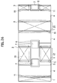
Fig. 13] Fig. 13 is a cross-sectional view taken along line A-A inFig. 12 . - [
Fig. 14] Fig. 14(a) is a perspective view for explaining a method of manufacturing the semiconductor device according to the second embodiment of the present invention. -
Fig. 14(b) is a perspective view continued fromFig. 14(a) for explaining the method of manufacturing the semiconductor device according to the second embodiment of the present invention. - [
Fig. 15] Fig. 15(a) is a cross-sectional view taken along line A-A inFig. 14(b) .Fig. 15(b) is a cross-sectional view taken along line B-B inFig. 14(b) .Fig. 15(c) is a cross-sectional view taken along line C-C inFig. 14(b) . - [
Fig. 16] Fig. 16(a) to Fig. 16(c) are cross-sectional views continued fromFig. 15(a) to Fig. 15(c) for explaining the method of manufacturing the semiconductor device according to the second embodiment of the present invention. - [
Fig. 17] Fig. 17(a) to Fig. 17(c) are cross-sectional views continued fromFig. 16(a) to Fig. 16(c) for explaining the method of manufacturing the semiconductor device according to the second embodiment of the present invention. - [
Fig. 18] Fig. 18(a) to Fig. 18(c) are cross-sectional views continued fromFig. 17(a) to Fig. 17(c) for explaining the method of manufacturing the semiconductor device according to the second embodiment of the present invention. - [
Fig. 19] Fig. 19(a) to Fig. 19(c) are cross-sectional views continued fromFig. 18(a) to Fig. 18(c) for explaining the method of manufacturing the semiconductor device according to the second embodiment of the present invention. - [
Fig. 20] Fig. 20(a) to Fig. 20(c) are cross-sectional views continued fromFig. 19(a) to -
Fig. 19(c) for explaining the method of manufacturing the semiconductor device according to the second embodiment of the present invention. - [
Fig. 21] Fig. 21(a) to Fig. 21(c) are cross-sectional views continued fromFig. 20(a) to Fig. 20(c) for explaining the method of manufacturing the semiconductor device according to the second embodiment of the present invention. - [
Fig. 22] Fig. 22(a) to Fig. 22(c) are cross-sectional views continued fromFig. 21(a) to Fig. 21(c) for explaining the method of manufacturing the semiconductor device according to the second embodiment of the present invention. - [
Fig. 23] Fig. 23(a) to Fig. 23(c) are cross-sectional views continued fromFig. 22(a) to Fig. 22(c) for explaining the method of manufacturing the semiconductor device according to the second embodiment of the present invention. - [
Fig. 24] Fig. 24(a) to Fig. 24(c) are cross-sectional views continued fromFig. 23(a) to Fig. 23(c) for explaining the method of manufacturing the semiconductor device according to the second embodiment of the present invention. - [
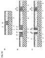
Fig. 25] Fig. 25(a) to Fig. 25(c) are cross-sectional views continued fromFig. 24(a) to Fig. 24(c) for explaining the method of manufacturing the semiconductor device according to the second embodiment of the present invention. - [
Fig. 26] Fig. 26 is a top view entirely showingFig. 25(a) to Fig. 25(c) . - [
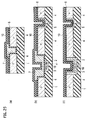
Fig. 27] Fig. 27(a) to Fig. 27(c) are cross-sectional views continued fromFig. 25(a) to Fig. 25(c) for explaining the method of manufacturing the semiconductor device according to the second embodiment of the present invention. - [
Fig. 28] Fig. 28(a) to Fig. 28(c) are cross-sectional views continued fromFig. 27(a) to Fig. 27(c) for explaining the method of manufacturing the semiconductor device according to the second embodiment of the present invention. - [
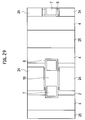
Fig. 29] Fig. 29 is a top view entirely showingFig. 28(a) to Fig. 28(c) . - [
Fig. 30] Fig. 30 is a perspective view showing an example of a semiconductor device according to a third embodiment of the present invention. - Hereinafter, embodiments of the present invention will be explained with reference to the drawings. The same or similar elements in the following explanations of the drawings are indicated by the same or similar reference numerals. In the embodiments of the present invention, "a first conductivity type" and "a second conductivity type" are opposite conductivity types. Namely, when the first conductivity type is an n-type, the second conductivity type is a p-type, and when the first conductivity type is a p-type, the second conductivity type is an n-type. The present invention will be illustrated with an example in which the first conductivity type is an n-type and the second conductivity type is a p-type; however, the first conductivity type may be a p-type and the second conductivity type may be an n-type instead. When the n-type and the p-type are switched, a polarity of applied voltage is also reversed.
-
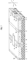
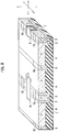
Fig. 1 is a perspective view schematically showing a configuration of a semiconductor device according to a first embodiment of the present invention. The first embodiment exemplifies a metal-oxide-semiconductor field-effect transistor (MOSFET) used as the semiconductor device.Fig. 1 does not show electrode wiring for convenience of explanation.Fig. 1 shows three semiconductor elements; however, the first embodiment is not limited thereto. For example, a number of semiconductor elements may be arranged in the x-axis and z-axis directions shown inFig. 1 . - As shown in
Fig. 1 , the semiconductor device according to the first embodiment of the present invention includes asubstrate 1, an n--type drift region 4 formed on one main surface of thesubstrate 1, a p-type well region 2 provided in thedrift region 4, an n+-type source region 3 provided in thewell region 2, an n+-type drain region 5 provided in thedrift region 4 and separated from thewell region 2, and agate electrode 7 provided in thedrift region 4 with agate insulating film 6 interposed therebetween. - The
substrate 1 has a thickness of several tens to several hundreds of micrometers. Thesubstrate 1 used may be a semi-insulating substrate or an insulating substrate. Here, an insulating substrate is a substrate having a sheet resistance of several kΩ/sq or greater, and a semi-insulating substrate is a substrate having a sheet resistance of several tens of Ω/sq or greater. The material used for thesubstrate 1 may be silicon carbide (SiC). The first embodiment of the present invention exemplifies a case where thesubstrate 1 is an insulating substrate formed of silicon carbide. - The
drift region 4 has a thickness of several to several tens of micrometers. An impurity concentration of thedrift region 4 is higher than that of thesubstrate 1 and is approximately in a range of 1×10¹⁴ to 1×1018 cm-3. Thedrift region 4 is formed of the same material as thesubstrate 1. When the substrate is formed of silicon carbide, thedrift region 4 is an epitaxially grown layer formed of silicon carbide. - The
well region 2 is provided in thedrift region 4 to extend from one main surface of the drift region 4 (hereinafter, referred to as "second main surface") opposite to another main surface in contact with the substrate 1 (hereinafter, referred to as "first main surface") in a direction perpendicular to the second main surface of the drift region 4 (in the y-axis direction inFig. 1 ). An edge of thewell region 2 further extends to the inside of thesubstrate 1 in the direction perpendicular to the second main surface of the drift region 4 (in the y-axis direction inFig. 1 ). Here, "the edge of thewell region 2" represents a portion defined by a bottom surface of thewell region 2 parallel to the second main surface of thedrift region 4 and part of side surfaces of thewell region 2 connected to the bottom surface and perpendicular to the second main surface of thedrift region 4. Thewell region 2 also extends in the direction parallel to the second main surface of the drift region 4 (in the z-axis direction inFig. 1 ). An impurity concentration of thewell region 2 is approximately in a range of 1×10¹⁵ to 1×1019 cm-3. - The
source region 3 is provided in thewell region 2 to extend from the second main surface of thedrift region 4 in the direction perpendicular to the second main surface of the drift region 4 (in the y-axis direction inFig. 1 ). Thesource region 3 extends parallel to thewell region 2 in the direction parallel to the second main surface of the drift region 4 (in the z-axis direction inFig. 1 ). Thesource region 3 is the same conductivity type as thedrift region 4. An impurity concentration of thesource region 3 is higher than thedrift region 4 and is approximately in a range of 1×10¹⁸ to 1×1021 cm-3. Thesource region 3 and thewell region 2 are electrically connected withsource electrodes 15 having the same potential. The material used for thesource electrodes 15 may be nickel (Ni), titanium (Ti) or molybdenum (Mo). - A
gate groove 8 is formed in thedrift region 4. Thegate groove 8 extends from the second main surface of thedrift region 4 in the direction perpendicular to the second main surface of the drift region 4 (in the y-axis direction inFig. 1 ). Thegate groove 8 is formed to penetrate thesource region 3 and thewell region 2 in the direction parallel to the second main surface of the drift region 4 (in the x-axis direction inFig. 1 ). The bottom surface of thegate groove 8 may be shallower than or conform to the bottom surface of thesource region 3. Thegate electrode 7 is formed on the surface of thegate groove 8 with thegate insulating film 6 interposed therebetween. The material used for thegate insulating film 6 may be a silicon oxide film (SiO2 film). The material used for thegate electrode 7 may be n-type polysilicon. - The
drain region 5 is provided to extend from the second main surface of thedrift region 4 in the direction perpendicular to the second main surface of the drift region 4 (in the y-axis direction inFig. 1 ). Thedrain region 5 extends parallel to thewell region 2 and thesource region 3 in the direction parallel to the second main surface of the drift region 4 (in the z-axis direction inFig. 1 ). Thedrain region 5 is the same conductivity type as thedrift region 4. An impurity concentration of thedrain region 5 is higher than thedrift region 4 and substantially the same as that of thesource region 3 that is approximately in the range of 1×10¹⁸ to 1×1021 cm-3. Thedrain region 5 is electrically connected with adrain electrode 16. The material used for thedrain electrode 16 may be nickel (Ni), titanium (Ti) or molybdenum (Mo). - Next, a fundamental operation of the semiconductor device according to the first embodiment of the present invention is explained below.
- The semiconductor device according to the first embodiment of the present invention functions as a transistor to control a potential of the
gate electrode 7 in a state where thedrain electrode 16 is applied with a positive potential based on a potential of thesource electrodes 15. In other words, when a voltage between thegate electrode 7 and thesource electrodes 15 reaches a predetermined threshold or greater, an inversion layer as a channel is formed in thewell region 2 located toward thegate electrode 7 so as to be turned on, and a current thus flows from thedrain electrode 16 to thesource electrodes 15. More particularly, electrons flow from thesource electrodes 15 to thesource region 3 and further flow into thedrift region 4 via the channel. The electrons in thedrift region 4 further flow through thedrain region 5 finally into thedrain electrode 16. - When the voltage between the
gate electrode 7 and thesource electrodes 15 reaches the predetermined threshold or lower, the inversion layer in thewell region 2 disappears to be turned off, and the current between thedrain electrode 16 and thesource electrodes 15 stops. At this time, a high voltage of several hundreds to several thousands of volts is applied between the drain and the source. - According to the first embodiment of the present invention, the semiconductor device has a lateral structure so that the channel width can be defined by the depth of the
drift region 4 and therefore can be increased even when a surface area of the structure is fixed. In addition, the edge of thewell region 2 extends to the inside of thesubstrate 1, so as to significantly reduce electric field concentration caused at the edge of thewell region 2 and prevent a decrease in voltage resistance. Further, since the edge of thewell region 2 extends to the inside of thesubstrate 1, and the impurity concentration of thesubstrate 1 is lower than that of thedrift region 4, a breakdown voltage between thesubstrate 1 and thewell region 2 is greater than that between thedrift region 4 and thewell region 2 when thedrift region 4 and thesubstrate 1 have the same length in the direction parallel to the second main surface of thedrift region 4. Accordingly, the voltage resistance can be further improved as compared with the structure described inPatent Literature 1. - Further, since the
substrate 1 is a semi-insulating substrate or an insulating substrate, the edge of thewell region 2 is formed in an insulating region. Thus, the voltage resistance of the edge of thewell region 2 can greatly be increased so that the semiconductor device having high voltage resistance can be ensured. - Further, since the material used for the
substrate 1 is silicon carbide exerting high insulating performance and having high heat conductivity, thesubstrate 1 with the rear surface adhered to a cooling system via a binder can efficiently radiate heat caused by a current generated when the semiconductor device is turned on, so as to cool the semiconductor device efficiently. In addition, since silicon carbide is a semiconductor having a wide bandgap and has a low intrinsic carrier concentration, the semiconductor device effectively exerting high insulating performance and having high voltage resistance can be ensured. - An example of a method of manufacturing the semiconductor device according to the first embodiment of the present invention is explained below with reference to
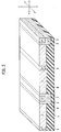
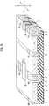
Fig. 2 to Fig. 7 . - First, the
substrate 1 is prepared as shown inFig. 2 . Thesubstrate 1 is an insulating substrate formed of undoped silicon carbide and has a thickness of several tens to several hundreds of micrometers. An n--type silicon carbide epitaxial layer is formed as thedrift region 4 on thesubstrate 1. Here, silicon carbide has several polytypes (polymorphism). The present embodiment is illustrated with an example of using silicon carbide of a common 4H polytype. Thedrift region 4 is formed, for example, to have an impurity concentration in a range of 1×10¹⁴ to 1×1018 cm-3 and a thickness of several to several tens of micrometers. - Next, as shown in
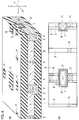
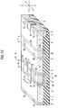
Fig. 3 , the p-type well region 2, the n+-type source region 3 and the n+-type drain region 5 are formed in thedrift region 4. Thewell region 2 is preferably formed first. Then, thesource region 3 and thedrain region 5 may be formed simultaneously. Thewell region 2, thesource region 3 and thedrain region 5 are formed by an ion injection method. In order to mask thedrift region 4 excluding regions into which ions are injected, a mask material may be formed on thedrift region 4 in the following steps. The mask material used may be a silicon oxide film (SiO2 film). The deposition may be performed by a thermal CVD method or a plasma CVD method. Next, a resist is applied on the mask material and then patterned by common photolithography. The patterned resist is used as a mask so as to selectively remove part of the mask material by etching. The etching performed may be wet etching using hydrofluoric acid or dry etching such as reactive ion etching (RIE). The resist is then removed by use of oxygen plasma or sulfuric acid. Next, by use of the mask material as a mask, p-type and n-type impurities are injected into thedrift region 4 by an ion injection method so as to form the p-type well region 2 and the n+-type source region 3. The p-type impurities may be aluminum (Al) or boron (B). The n-type impurities may be nitrogen (N). Here, the ion injection is performed in a state where the substrate is heated to approximately 600 °C so as to prevent crystal defect from being caused in the injection regions. After the ion injection is carried out, the mask material is removed by, for example, wet etching using hydrofluoric acid. The impurities injected by the ion injection method are then activated by heat treatment (annealing). The heat treatment may be performed at, for example, 1700 °C and preferably under an argon (Ar) or nitrogen (N) atmosphere. The impurity concentration of each of thesource region 3 and thedrain region 5 is preferably in the range of 1×10¹⁸ to 1×1021 cm-3, and the injection depth is shallower than the first main surface of thedrift region 4. The impurity concentration of thewell region 2 is preferably in the range of 1×10¹⁵ to 1×1019 cm-3, and the injection depth is deeper than the first main surface of thedrift region 4 so that the edge of thewell region 2 reaches the inside of thesubstrate 1. When the thickness of thedrift region 4 is 1 µm or greater, injection energy may be at a level of MKeV or greater. - Next, as shown in
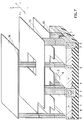
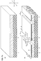
Fig. 4 , amask material 9 is formed in order to form thegate groove 8 in thedrift region 4. Themask material 9 may be obtained in a manner such that an insulating film is patterned as in the case of the mask material used in the step shown inFig. 3 . Then, themask material 9 is used as a mask to form thegate groove 8. Here, the structure after thegate groove 8 is formed is not shown in the drawing. Thegate groove 8 is formed preferably by dry etching such as RIE. The depth of thegate groove 8 is shallower than thesource region 3. Themask material 9 is removed after thegate groove 8 is formed. For example, when themask material 9 is a silicon oxide film, themask material 9 is removed by hydrofluoric acid cleaning. - Next, as shown in
Fig. 5(a) and Fig. 5(b) , thegate insulating film 6 and thegate electrode 7 are formed.Fig. 5(b) is a cross-sectional view taken along line A-A inFig. 5(a) . In particular, thegate insulating film 6 is first formed on surfaces of thedrift region 4 and thegate groove 8 by a thermal oxidation method or a deposition method. For example, in the case of using the thermal oxidation method, the substrate is heated to approximately 1100 °C under an oxygen atmosphere so that a silicon oxide film is formed at all the portions of the substrate where oxygen comes into contact. Thegate insulating film 6 thus formed may be subjected to annealing at approximately 1000 °C under an atmosphere of nitrogen, argon or nitrous oxide (N2O) in order to decrease an interfacial level at the interface between thewell region 2 and thegate insulating film 6. Next, the material of which thegate electrode 7 is formed is deposited on the surface of thegate insulating film 6. The material of which thegate electrode 7 is formed is commonly polysilicon, and the present embodiment is also illustrated with polysilicon. The polysilicon may be deposited by a low pressure CVD method. The deposition thickness of the polysilicon is set to be greater than half of the width of thegate groove 8 so as to fill thegate groove 8 completely with the polysilicon. For example, when the width of thegate groove 8 is 2 µm, the deposition thickness of the polysilicon is thicker than 1 µm. The deposited polysilicon is then subjected to annealing in POCl3 at approximately 950 °C so as to form n-type polysilicon and provide thegate electrode 7 with electric conductivity Next, the polysilicon of thegate electrode 7 is subjected to etching such as isotropic etching or anisotropic etching. The etching amount is set such that the polysilicon remains in thegate groove 8. For example, when the width of thegate groove 8 is 2 µm, and the polysilicon is deposited with the thickness of 1.5 µm, the etching amount is preferably 1.5 µm. Here, several percent of overetching with respect to the polysilicon with the thickness of 1.5 µm is a permissible level for etching control.Fig. 5(a) and Fig. 5(b) each show the structure after the polysilicon is subjected to etching. Although the depth of thegate groove 8 is shown differently betweenFig. 5(a) and Fig. 5(b) , the bottom of thegate groove 8 may conform to that of thesource region 3 as shown inFig. 5(a) or may be shallower than that of thesource region 3 as shown inFig. 5(b) . - Next, as shown in
Fig. 6(a) , aninterlayer insulating film 10 and contact holes 11 for electrodes are formed.Fig. 6(b) shows the positions of the contact holes 11 as viewed from above.Fig. 6(b) does not show the interlayer insulatingfilm 10 for convenience of explanation. Theinterlayer insulating film 10 is generally preferably a silicon oxide film and may be deposited by a thermal CVD method or a plasma CVD method. After theinterlayer insulating film 10 is deposited, a resist is applied on theinterlayer insulating film 10 and then patterned by common photolithography (not shown in the drawings). The patterned resist is used as a mask so as to selectively remove part of theinterlayer insulating film 10 by wet etching using hydrofluoric acid or dry etching such as reactive ion etching (RIE) to form the contact holes 11. The resist is then removed by use of oxygen plasma or sulfuric acid.Fig. 6(a) and Fig. 6(b) each show the configuration after the contact holes 11 are formed. - After the contact holes 11 are formed,
gate wiring 12,source wiring 13 anddrain wiring 14 are formed, as shown inFig. 7. Fig. 7 does not show any interlayer insulating film between the layers of thegate wiring 12, thesource wiring 13 and thedrain wiring 14 for convenience of explanation. The wiring material used may be metal such as titanium (Ti), nickel (Ni) or molybdenum (Mo). A specific method of forming thegate wiring 12, thesource wiring 13 and thedrain wiring 14 by use of Ti is explained below. First, Ti is deposited by, for example, MOCVD. Next, Ti is subjected to selective etching by use of a resist as a mask. Next, the interlayer insulating film between thegate wiring 12 and thesource wiring 13 is deposited, and the contact holes are formed. The interlayer insulating film is deposited preferably by sputtering, and the contact holes may be formed in the same manner as the step shown inFig. 6(a) . Next, a metal material for thesource wiring 13 is deposited and subjected to etching in the same manner as in the case of thegate wiring 12. Then, the interlayer insulating film between thesource wiring 13 and thedrain wiring 14 is deposited, the contact holes are formed, and a metal material for thedrain wiring 14 is further deposited.Fig. 7 shows the semiconductor device after thedrain wiring 14 is formed. Accordingly, the semiconductor device shown inFig. 1 is completed through the above-described steps. - The semiconductor device shown in
Fig. 1 manufactured by the method according to the first embodiment of the present invention can exert improved voltage resistance. - The first embodiment of the present invention exemplified the case where the
substrate 1 is an insulating or semi-insulating substrate. The first embodiment is further illustrated with a modified example in which thesubstrate 1 is the same conductivity type (n-type) semiconductor substrate as thedrift region 4. Thesubstrate 1 is formed of, for example, silicon carbide, and the impurity concentration of thesubstrate 1 is lower than that of thedrift region 4. The operation and fabrication methods for the semiconductor device in this example are substantially the same as those for the semiconductor device in which thesubstrate 1 is an insulating or semi-insulating substrate. - If the
substrate 1 is a conductivity type (p-type) semiconductor substrate different from thedrift region 4, a depletion layer extends from thesubstrate 1 toward thedrift region 4 when a current flows from thesource region 3 to thedrift region 4 via thewell region 2 in which a channel is formed when the semiconductor device is turned on. As a result, a passage of the current narrows, and the current thus decreases. Further, thesubstrate 1, if being a conductivity type (p-type) semiconductor substrate different from thedrift region 4, should be designed with close attention to voltage resistance between thesubstrate 1 and thedrift region 4. On the other hand, thesubstrate 1 that is the same conductivity type (n-type) semiconductor substrate as thedrift region 4 can allow the passage of the current to spread into thesubstrate 1. Accordingly, the current increases, so that a reduction in loss can be expected. Furthermore, such a substrate can facilitate a designing process in view of voltage resistance between thesubstrate 1 and thedrift region 4, so that a semiconductor device having high voltage resistance can be provided. -
Fig. 8 shows a semiconductor device having a structure modified from that shown inFig. 1 . The semiconductor device shown inFig. 8 differs from that shown inFig. 1 in that thesource region 3 and thedrain region 5 extend to the inside of thesubstrate 1. A method of manufacturing the semiconductor device shown inFig. 8 differs from that in the first embodiment in that, when thesource region 3 and thedrain region 5 are formed by ion injection, impurities are injected deeply below the first main surface of thedrift region 4, but other steps are substantially the same. - In the semiconductor device shown in
Fig. 8 , since thesource region 3 extends to the inside of thesubstrate 1, a lateral area of thesource region 3 perpendicular to the second main surface of thedrift region 4 increases. Accordingly, a current can be increased when the semiconductor device is turned on, and a loss can be reduced. - In addition, since the
drain region 5 extends to the inside of thesubstrate 1, a lateral area of thedrain region 5 perpendicular to the second main surface of thedrift region 4 increases. Accordingly, a current can be increased when the semiconductor device is turned on, and a loss can be reduced. - In the semiconductor device shown in
Fig. 8 , both thesource region 3 and thedrain region 5 extend to the inside of thesubstrate 1, which can take full advantage of the lateral areas of thesource region 3 and thedrain region 5 so that a large amount of current can flow in the semiconductor device. Although the semiconductor device shown inFig. 8 is illustrated with the example in which both thesource region 3 and thedrain region 5 extend to the inside of thesubstrate 1, the semiconductor device in which either thesource region 3 or thedrain region 5 extends to the inside of thesubstrate 1 can also allow a large amount of current to flow therethrough as compared with the structure shown inFig. 1 . -
Fig. 9 shows a semiconductor device having a structure modified from that shown inFig. 8 . The semiconductor device shown inFig. 9 differs from that shown inFig. 8 in that thegate groove 8 extends downward more deeply so that part of thegate groove 8 penetrates into thesubstrate 1. The operation of the semiconductor device shown inFig. 9 is substantially the same as that of the semiconductor device shown inFig. 8 . The fabrication method for the semiconductor device shown inFig. 9 differs from that for the semiconductor device shown inFig. 8 in the process of forming thegate groove 8 extending deeply below the first main surface of thedrift region 4, but other steps are substantially the same. - In the semiconductor device shown in
Fig. 9 , part of thegate groove 8 extends to the inside of thesubstrate 1 so that the bottom surface and corner portions defined by the bottom surface and side surfaces of thegate groove 8 are located inside thesubstrate 1. When thesubstrate 1 is an insulating substrate or an n-type semiconductor substrate of which impurity concentration is lower than that of thedrift region 4, an electric field concentration at the bottom surface and corner portions of thegate groove 8 can be reduced more than that in the structure shown inFig. 1 orFig. 8 , so as to improve the voltage resistance. In addition, the structure shown inFig. 1 orFig. 8 includes a region where part of the bottom surface of thegate groove 8 is in contact with thesubstrate 1 via thegate insulating film 6. A capacitance generated in this region is a gate-drain capacitance, which causes a loss at the time of operating the semiconductor device. In thesubstrate 1 shown inFig. 9 , however, there is little capacitance in the above-mentioned region in contact with thesubstrate 1 when thesubstrate 1 is an insulating substrate, so as to reduce a loss at the time of operating the semiconductor device. -
Fig. 10 shows a semiconductor device having a structure modified from that shown inFig. 9 . The semiconductor device shown inFig. 10 differs from that shown inFig. 9 in that the bottom of thegate groove 8 penetrates into thewell region 2. The operation of the semiconductor device shown inFig. 10 is substantially the same as that of the semiconductor device shown inFig. 9 . The fabrication method for the semiconductor device shown inFig. 10 differs from that for the semiconductor device shown inFig. 9 in the process of forming thegate groove 8 extending downward more deeply than thesource region 3, but other steps are substantially the same. - In the semiconductor device shown in
Fig. 10 , when thegate groove 8 is deeper than thesource region 3 in the direction perpendicular to the second main surface of thedrift region 4, and the bottom surface of thegate groove 8 is located in thewell region 2, a gate-source capacitance generated in a region where the bottom surface of thegate groove 8 is in contact with thewell region 2 via thegate insulating film 6 varies depending on a voltage of thegate electrode 7. For example, when thewell region 2 is a p-type semiconductor, and a gate voltage is negative, a depletion layer extends in thewell region 2 so that the gate-source capacitance generated at the bottom surface of thegate groove 8 is small. On the other hand, when the gate voltage is positive and greater than or equal to a threshold voltage of the semiconductor device, thewell region 2 is reversed, and the gate-source capacitance generated at the bottom surface of thegate groove 8 is maximized and is a capacitance in thegate insulating film 6. In the structure as shown inFig. 1 ,Fig. 8 orFig. 9 in which the bottom of thegate groove 8 is located in thesource region 3, a capacitance in a region defined by thegate electrode 7, thegate insulating film 6 and thesource region 3 does not vary depending on the gate voltage but is constantly the capacitance in thegate insulating film 6. The structure shown inFig. 10 , however, can decrease the gate-source capacitance at the bottom of thegate groove 8 so that a semiconductor device with a loss reduced can be provided. -
Fig. 11 shows a semiconductor device having a structure modified from that shown inFig. 10 . The semiconductor device shown inFig. 11 differs from that shown inFig. 10 in that the bottom of thegate groove 8 is located below thewell region 2. The fabrication method for the semiconductor device shown inFig. 11 differs from that for the semiconductor device shown inFig. 10 in the step of forming thegate groove 8 having a greater depth than thewell region 2. - Here, if the bottom of the
gate groove 8 is located in thedrift region 4, and the semiconductor device is formed of particularly a SiC material in which thegate insulating film 6 is a thermal silicon oxide film, the thickness of the thermal silicon oxide film varies depending on a crystal face of SiC. For example, when the surface of thedrift region 4 is a (0001) plane, the oxide film formed at the bottom surface of thegate groove 8 parallel to the second main surface of thedrift region 4 is thinner than the oxide film formed at the side surface perpendicular to the second main surface of thedrift region 4. As a result, the voltage resistance between thegate electrode 7 and thesource electrodes 15 is decreased at the bottom surface of thegate groove 8. Further, a gate-source capacitance generated at the bottom surface of thegate groove 8 increases and accounts for a large proportion of the entire gate-source capacitance, which may increase a loss at the time of operating the semiconductor element. - According to the structure shown in
Fig. 11 , however, the bottom surface of thegate groove 8 located below thewell region 2 is in contact with thesubstrate 1 but not electrically connected to thesource region 3. Therefore, a gate-source capacitance between thegate electrode 7 and thesource electrodes 15 is hardly generated at the bottom surface of thegate groove 8. A decrease of the gate-source capacitance generated at the bottom surface of thegate groove 8 leads to a great decrease of the entire gate-source capacitance, so that a semiconductor device having high reliability with a loss reduced can be provided. Further, when thesubstrate 1 is an insulating substrate, the gate-drain capacitance generated at the bottom surface of thegate groove 8 can also be decreased, so that the semiconductor device with a loss reduced can be ensured. -
Fig. 12 is a perspective view schematically showing a configuration of a semiconductor device according to a second embodiment of the present invention.Fig. 12 does not show electrode wiring for convenience of explanation. The configuration of the electrode wiring is the same as that shown inFig. 7 . - The semiconductor device according to the second embodiment of the present invention differs from that according to the first embodiment in that a
source groove 17 is formed in thesource region 3, and adrain groove 20 is formed in thedrain region 5, as shown inFig. 12 . - A bottom portion of the
source groove 17 is provided with a p+-typewell contact region 19 having a higher impurity concentration than thewell region 2 and in contact with thewell region 2. Anelectrical conducting layer 24 is laid in thesource groove 17. Theelectrical conducting layer 24 has the same potential as thesource electrodes 15 and is brought in ohmic contact with thesource region 3 and thewell contact region 19. Anelectrical conducting layer 25 is laid in thedrain groove 20. Theelectrical conducting layer 25 has the same potential as thedrain electrodes 16 and is brought in ohmic contact with thedrain region 5. The material used for the electrical conducting layers 24, 25 may be an electrical conducting material such as nickel (Ni), titanium (Ti) or molybdenum (Mo). - As shown in
Fig. 12 , when the width of thesource groove 17 is defined as "a", the width of thedrain groove 20 is defined as "b", and the width of thegate groove 8 is defined as "c", the relationship of a>b>c is fulfilled. That is, the width a of thesource groove 17 is greater than the width b of thedrain groove 20, and the width b of thedrain groove 20 is greater than the width c of thegate groove 8. -
Fig. 13 is a partial cross-sectional view of thesource groove 17 taken along line A-A inFig. 12 . As shown inFig. 13 , thegate electrode 7 is in ohmic contact with anelectrical conducting layer 18 and has the same potential as theelectrical conducting layer 18. Thegate electrode 7 is insulated from theelectrical conducting layer 24 with theinterlayer insulating film 10. - The other configurations of the semiconductor device according to the second embodiment of the present invention are substantially the same as those according to the first embodiment. The operation of the semiconductor device according to the second embodiment of the present invention is substantially the same as that of the semiconductor device according to the first embodiment.
- According to the second embodiment of the present invention, the edge of the
well region 2 extends to the inside of thesubstrate 1 so as to significantly reduce an electric field concentration caused at the edge of thewell region 2 and prevent a decrease in voltage resistance. Further, since the edge of thewell region 2 extends to the inside of thesubstrate 1, and the impurity concentration of thesubstrate 1 is lower than that of thedrift region 4, a breakdown voltage between thesubstrate 1 and thewell region 2 is greater than that between thedrift region 4 and thewell region 2 when thedrift region 4 and thesubstrate 1 have the same length in the direction parallel to the second main surface of thedrift region 4. Accordingly, the voltage resistance can be further improved as compared with the structure described inPatent Literature 1. - Further, since the
substrate 1 is a semi-insulating substrate or an insulating substrate, the edge of thewell region 2 is formed in an insulating region. Thus, the voltage resistance of the edge of thewell region 2 can greatly be increased so that the semiconductor device having high voltage resistance can be ensured. - Further, since the material used for the
substrate 1 is silicon carbide exerting high insulating performance and having high heat conductivity, thesubstrate 1 with the rear surface adhered to a cooling system via an electrical conducting material can efficiently radiate heat caused by a current generated when the semiconductor device is turned on, so as to cool the semiconductor device efficiently. In addition, since silicon carbide is a semiconductor having a wide bandgap and has a low intrinsic carrier concentration, the semiconductor device effectively exerting high insulating performance and having high voltage resistance can be ensured. - Further, since the
source region 3 includes thesource groove 17, the injection depth of impurities can be decreased when thesource region 3 and thewell region 2 are formed, as compared with the case of the first embodiment. Since high injection energy is not required, the semiconductor device provided can contribute to a reduction in cost. Further, theelectrical conducting layer 24 is laid in thesource groove 17 and has the same electrical potential as thesource region 3. Here, if thesource groove 17 is not provided, a resistance component of thesource region 3 is applied in the direction perpendicular to thesubstrate 1. Such a resistance component acts to decrease a current when the semiconductor device operates, which leads to a decrease of the current. When theelectrical conducting layer 24 is laid in thesource groove 17, however, the resistance component of thesource region 3 in the perpendicular direction is aligned in parallel with a resistance component of theelectrical conducting layer 24. Since resistance of theelectrical conducting layer 24 is generally less than resistance of a semiconductor, the parallel resistance components can be decreased. Accordingly, the semiconductor device with a loss reduced can be ensured. - Further, since the width a of the
source groove 17 is greater than the width c of thegate groove 8, thesource groove 17 and thegate groove 8 can be formed simultaneously, and thesource region 3 and thewell region 2 can be formed with no mask used, so as to facilitate the manufacturing process. As a specific fabrication method, thegate groove 8 and thesource groove 17 are formed simultaneously by use of a mask pattern. For example, when the width a of thegate groove 8 is 1 µm, and the width c of thesource groove 17 is 2 µm, 0.5 µm of a silicon oxide film is deposited thereon by a LPCVD method after thegate groove 8 and thesource groove 17 are formed. As a result, thegate groove 8 is filled completely with the silicon oxide film, while thesource groove 17 is not completely filled with the silicon oxide film. Next, n-type impurities are injected by oblique ion injection so as to form thesource region 3. Then, p-type impurities are injected by oblique ion injection so as to form thewell region 2. Accordingly, thegate groove 8 and thesource groove 17 can be formed simultaneously, and thesource region 3 and thewell region 2 can be formed by self-alignment. Namely, a semiconductor device manufactured by a simple process at low cost can be provided. - Further, since the
drain region 5 includes thedrain groove 20, the injection depth of impurities can be decreased when thesource region 3 and thewell region 2 are formed, as compared with the case of the first embodiment. Since high injection energy is not required, the semiconductor device provided can contribute to a reduction in cost. Further, theelectrical conducting layer 25 is laid in thedrain groove 20 and has the same electrical potential as thedrain region 5. Here, if thedrain groove 20 is not provided, a resistance component of thedrain region 5 is applied in the direction perpendicular to the second main surface of thedrift region 4. Such a resistance component acts to decrease a current when the semiconductor device operates, which leads to a decrease of the current. When theelectrical conducting layer 25 is laid in thedrain groove 20, however, the resistance component of thedrain region 5 in the perpendicular direction is aligned in parallel with a resistance component of theelectrical conducting layer 25. Since resistance of theelectrical conducting layer 25 is generally less than resistance of a semiconductor, the parallel resistance components can be decreased. Accordingly, the semiconductor device with a loss reduced can be ensured. - Further, since the width b of the
drain groove 20 is greater than the width c of thegate groove 8, thedrain groove 20 and thegate groove 8 can be formed simultaneously, and thedrain region 5 can be formed with no mask used, so as to facilitate the manufacturing process. In particular, thedrain groove 20 and thegate groove 8 are formed simultaneously by use of a mask pattern. For example, when the width c of thegate groove 8 is 1 µm and the width b of thedrain groove 20 is 2 µm, 0.5 µm of a silicon oxide film is deposited thereon by a LPCVD method after thegate groove 8 and thedrain groove 20 are formed. As a result, thegate groove 8 is filled completely with the silicon oxide film, while thedrain groove 20 is not completely filled with the silicon oxide film. Next, n-type impurities are injected by oblique ion injection so as to form thedrain region 5. Accordingly, thedrain region 5 can be formed by self-alignment. Namely, a semiconductor device manufactured by a simple process at low cost can be provided. - Further, the
drain groove 20 is formed in thedrain region 5, and thesource groove 17 is formed in thesource region 3. Thesource groove 17 and thedrain groove 20 are provided with the respective electrically conductinglayers layer 24 and the electrically conductinglayer 25 have the same potential as thesource region 3 and thedrain region 5, respectively. The effect derived from this structure is explained with reference to thedrain region 5 as an example. If thedrain groove 20 is not provided, the resistance component of thedrain region 5 is applied in the direction perpendicular to the second main surface of thedrift region 4. Such a resistance component acts to decrease a current when the semiconductor device operates, which leads to a decrease of the current. When thedrain groove 20 is filled with theelectrical conducting layer 25, however, the resistance component of thedrain region 5 in the perpendicular direction is aligned in parallel with the resistance component of theelectrical conducting layer 25. Since the resistance of theelectrical conducting layer 25 is generally less than resistance of a semiconductor, the parallel resistance components can be decreased. The same effect as thedrain region 5 can be ensured in thesource region 3, and the current can be increased when the semiconductor device is turned on. Namely, the semiconductor device with a loss reduced can be ensured. - Further, since the width a of the
source groove 17 is greater than the width b of thedrain groove 20, and the width b of thedrain groove 20 is greater than the width c of thegate groove 8, thegate groove 8, thesource groove 17 and thedrain groove 20 can be formed simultaneously, and thesource region 3, thedrain region 5 and thewell region 2 can be formed by self-alignment. Accordingly, a semiconductor device manufactured by a simple process at low cost with high reliability but no concern about misalignment can be provided. - Further, since the
source groove 17 is provided with thewell contact region 19 at the bottom portion thereof, thewell contact region 19 can be formed by self-alignment, so that the semiconductor device manufactured by a simple process at low cost with high reliability but no concern about misalignment can be ensured. When thewell contact region 19 is a p-type region with a high impurity concentration, thewell contact region 19 can easily be brought in ohmic contact with theelectrical conducting layer 24, the contact resistance thereof can be reduced, and the potential of thewell region 2 can easily be controlled by thesource electrode 15. Accordingly, the semiconductor device with high reliability can be ensured. - An example of a method of manufacturing the semiconductor device according to the second embodiment of the present invention is explained below with reference to
Fig. 14(a) to Fig. 29 . - First, the
substrate 1 is prepared as shown inFig. 14(a) . Thesubstrate 1 is an insulating substrate formed of undoped silicon carbide and has a thickness of several tens to several hundreds of micrometers. An n--type silicon carbide epitaxial layer is formed as thedrift region 4 on thesubstrate 1. Here, silicon carbide has several polytypes (polymorphism). The present embodiment is illustrated with an example of using silicon carbide of a common 4H polytype. Thedrift region 4 is formed, for example, to have an impurity concentration in a range of 1×10¹⁴ to 1×1018 cm-3 and a thickness of several to several tens of micrometers. - Next, a step of forming the
gate groove 8, thedrain groove 20 and thesource groove 17 simultaneously in the drift region 4 (hereinafter, referred to as "first step") is performed.Fig. 14(b) is a perspective view showing a state after themask 9 is formed so as to form thegate groove 8, thedrain groove 20 and thesource groove 17 simultaneously. Themask material 9 may be obtained in a manner such that an insulating film is patterned as in the case of the mask material used in the step shown inFig. 3 . Then, themask material 9 is used as a mask to form thegate groove 8, thedrain groove 20 and thesource groove 17 by, for example, dry etching. As shown inFig. 14(b) , when the width of thesource groove 17 is defined as "a", the width of thedrain groove 20 is defined as "b", and the width of thegate groove 8 is defined as "c", thegate groove 8, thedrain groove 20 and thesource groove 17 are formed so that the relationship of a>b>c is fulfilled. The respective cross-sectional views taken along line A-A, line B-B and line C-C inFig. 14(b) are shown inFig. 15(a) to Fig. 15(c) . The subsequent steps are explained below with reference to the respective cross-sectional views. - After the first step, a step of depositing the mask material 21 (hereinafter, referred to as "second step") is performed. The
mask material 21 used may be a silicon oxide film, and the deposition method may be a thermal CVD method, a plasma CVD method or a low pressure CVD method. In order to improve coverage of the film, the low pressure CVD method is preferable. The deposition thickness is one half or more of the width c of thegate groove 8 and less than one half of the width b of thedrain groove 20. For example, when the width c of thegate groove 8 is 1 µm, and the width b of thedrain groove 20 is 2 µm, the thickness of themask material 21 is set to 0.5 µm or greater and less than 1 µm.Fig. 16(a) to Fig. 16(c) each show a state after themask material 21 is deposited with the thickness set as described above. As shown inFig. 16(a) to Fig. 16(c) , thegate groove 8 is filled completely with themask material 21, but thesource groove 17 and thedrain groove 20 are not completely filled with themask material 21. - After the second step, a step of forming the
drain region 5 and thesource region 3 simultaneously (hereinafter, referred to as "third step") is performed. The third step uses an ion injection method. Themask material 21 deposited in the second step is used as a mask in the injection regions without being patterned by photolithography, which differs from the first embodiment. Since thesource region 3 and thedrain region 5 are an n-type, nitrogen (N) or phosphorus (N) may be used as n-type impurities. The ion injection is carried out in a state where the substrate is heated to approximately 600 °C so as to prevent crystal defect from being caused in the injection regions. The ion injection is also carried out in a manner such that a traveling direction of an ion beam is inclined at a fixed angle to the direction perpendicular to the main surface of thesubstrate 1 so that the impurities are injected also to side walls of thedrain groove 20 and thesource groove 17. The impurity concentration is preferably in the range of 1×10¹⁸ to 1×1021 cm-3. The injection depth is greater than the thickness of themask material 21 and less than the total thickness of themask material 21 and themask material 9. The reason for this is that the n-type impurities, if being injected deeply below themask material 9, are injected further to the surface of thedrift region 4.Fig. 17(a) to Fig. 17(c) each show a state of the semiconductor device after the third step is performed. As shown inFig. 17(a) to Fig. 17(c) , the n-type impurities are injected to the side walls and bottom portions of thesource groove 17 and thedrain groove 20. - After the third step, a step of depositing a mask material 22 (hereinafter, referred to as "fourth step") is performed. The
mask material 22 used may be a silicon oxide film, and the deposition method may be a thermal CVD method, a plasma CVD method or a low pressure CVD method. In order to improve coverage of the film, the low pressure CVD method is preferable. The deposition thickness is set to greater than or equal to a value obtained in such a manner as to subtract the thickness of themask material 21 from one half of the width b of thedrain groove 20 and less than a value obtained in such a manner as to subtract the thickness of themask material 21 from one half of the width c of thesource groove 17. For example, when the width of thedrain groove 20 is 2 µm, the thickness of themask material 21 is set to 0.8 µm, and the width c of thesource groove 17 is 3 µm, the thickness of themask material 22 is set to 0.2 µm or greater and less than 0.7 µm.Fig. 18(a) to Fig. 18(c) each show a state after themask material 22 is deposited with the thickness set as described above. As shown inFig. 18(a) to Fig. 18(c) , thegate groove 8 and thedrain groove 20 are filled completely with themask material 22, but thesource groove 17 is still not completely filled with themask material 22. - After the fourth step, a step of forming the well region 2 (hereinafter, referred to as "fifth step") is performed. This step uses an ion injection method. The patterning by photolithography is not performed on the injection regions, which differs from the first embodiment. The
mask material 21 and themask material 22 deposited in the second step and the fourth step are each used as a mask. Since thewell region 2 is a p type, aluminum (Al) or boron (B) may be used as p-type impurities. The ion injection is carried out in a state where the substrate is heated to approximately 600 °C so as to prevent crystal defect from being caused in the injection regions. The ion injection is also carried out in a manner such that a traveling direction of an ion beam is inclined at a fixed angle to the direction perpendicular to the main surface of thesubstrate 1 so that the impurities are injected to the side walls and the bottom of thesource groove 17. The impurity concentration is preferably in the range of 1×10¹⁵ to 1×1019 cm-3. The injection depth is greater than the total thickness of themask material 21, themask material 22 and the source region and less than the total thickness of themask material 21, themask material 22 and themask material 9.Fig. 19(a) to Fig. 19(c) each show a state of the semiconductor device after the fifth step is performed. As shown inFig. 19(a) to Fig. 19(c) , the p-type impurities are injected to the side walls and the bottom of thesource groove 17. - After the fifth step, a step of forming the well contact region 19 (hereinafter, referred to as "sixth step") is performed. Before the sixth step, etching may be performed on the
mask material 21 and themask material 22. The etching is performed entirely on the mask materials, instead of selective etching by photolithography. When themask material 21 and themask material 22 are both a silicon oxide film, anisotropy dry etching such as reactive ion etching (RIE) is preferable. The etching thickness may be the total thickness of themask material 21 and themask material 22.Fig. 20(a) to Fig. 20(c) each show a sectional structure after the anisotropy dry etching is performed. As shown inFig. 20(a) to Fig. 20(c) , thegate groove 8 and thedrain groove 20 are still filled completely with themask material 21 and themask material 22. Although themask material 21 and themask material 22 remain on the side walls of thesource groove 17, thesource region 3 is exposed on the bottom surface of thesource groove 17. Themask material 9 also remains on the surface of thedrift region 4. The sixth step is thus performed on the configuration described above to form thewell contact region 19 by the ion injection method. Since thewell contact region 19 is a p type, aluminum (Al) or boron (B) may be used as p-type impurities. The ion injection is carried out in a state where the substrate is heated to approximately 600 °C so as to prevent crystal defect from being caused in the injection regions. The ion injection is preferably carried out in a manner such that a traveling direction of an ion beam is set to the direction perpendicular to thesubstrate 1. Since the bottom portion of thesource groove 17 is provided with the n-type source region 3, the concentration of the p-type impurities injected is preferably at least twice as much as the impurity concentration of thesource region 3. Accordingly, the n-type source region 3 partly includes a p-type region in which the p-type impurities are injected. The injection depth may be deeper than thesource region 3 and shallower than thewell region 2.Fig. 21(a) to Fig. 21(c) each show a state of the semiconductor device after the sixth step is performed. - Next, the
mask material 9, themask material 21 and themask material 22 are removed. For example, when themask material 9, themask material 21 and themask material 22 are a silicon oxide film, these materials can be removed by hydrofluoric acid cleaning. The impurities injected by ion injection are then activated by heat treatment (annealing). The heat treatment may be performed at approximately 1700 °C and preferably under an argon (Ar) or nitrogen (N) atmosphere. Next, thegate insulating film 6 is formed.Fig. 22(a) to Fig. 22(c) each show a sectional structure after thegate insulating film 6 is formed. Thegate insulating film 6 may be formed by either a thermal oxidation method or a deposition method. For example, in the case of using the thermal oxidation method, the substrate is heated to approximately 1100 °C under an oxygen atmosphere so that a silicon oxide film is formed at all the portions of the substrate where oxygen comes into contact. Thegate insulating film 6 thus formed may be subjected to annealing at approximately 1000 °C under an atmosphere of nitrogen (N), argon (Ar) or N2O in order to decrease an interfacial level at the interface between thewell region 2 and thegate insulating film 6. Next, amaterial 23 of which thegate electrode 7 is formed is deposited thereon.Fig. 23(a) to Fig. 23(c) each show a sectional structure after deposition. Thematerial 23 of which thegate electrode 7 is formed is commonly polysilicon, and the present embodiment is also illustrated with polysilicon. Thepolysilicon 23 may be deposited by a low pressure CVD method. The deposition thickness of thepolysilicon 23 is set to be greater than half of the width of thegate groove 8 so as to fill thegate groove 8 completely with thepolysilicon 23. For example, when the width of thegate groove 8 is 2 µm, the deposition thickness of thepolysilicon 23 is greater than 1 µm. The depositedpolysilicon 23 is then subjected to annealing in POCl3 at 950 °C so as to form the n-type polysilicon 23 and provide thegate electrode 7 with electric conductivity. Next, thepolysilicon 23 other than thegate electrode 7 is subjected to etching. The etching performed may be either isotropic etching or anisotropic etching. The etching amount is set such that thepolysilicon 23 remains in thegate groove 8. For example, when the width c of thegate groove 8 is 2 µm, and the polysilicon is deposited with the thickness of 1.5 µm, the etching amount is preferably 1.5 µm. However, several percent of overetching with respect to the polysilicon with the thickness of 1.5 µm is a permissible level for etching control.Fig. 24(a) to Fig. 24(c) each show a sectional structure after thepolysilicon 23 is subjected to etching and thegate electrode 7 is formed. - Next, the
interlayer insulating film 10 and contact holes for forming electrodes are formed.Fig. 25(a) to Fig. 25(c) each show a sectional structure after theinterlayer insulating film 10 is formed.Fig. 26 shows the positions of the contact holes 11 as viewed from above.Fig. 26 does not show the interlayer insulatingfilm 10 for convenience of explanation. Theinterlayer insulating film 10 is generally preferably a silicon oxide film and may be deposited by a thermal CVD method or a plasma CVD method. After theinterlayer insulating film 10 is deposited, the contact holes are formed. A resist is applied on theinterlayer insulating film 10 and then patterned by common photolithography. The patterned resist is used as a mask so as to subject theinterlayer insulating film 10 to etching. The etching performed may be wet etching using hydrofluoric acid or dry etching such as reactive ion etching (RIE). The resist is then removed by use of oxygen plasma or sulfuric acid.Fig. 27(a) to Fig. 27(c) each show a sectional structure after the contact holes are formed. - After the contact holes are formed, the
electrical conducting layer 18, theelectrical conducting layer 24 and theelectrical conducting layer 25 are formed. The material commonly used for theelectrical conducting layer 18, theelectrical conducting layer 24 and theelectrical conducting layer 25 is metal such as titanium (Ti), nickel (Ni) or molybdenum (Mo). The present embodiment exemplifies the case of using Ti. First, Ti is deposited. The deposition is preferably performed by, for example, MOCVD. Next, Ti is subjected to selective etching by use of a mask. The mask material is preferably a resist.Fig. 28(a) to Fig. 28(c) each show a sectional structure after etching, andFig. 29 shows the entire surface structure thereof.Fig. 29 does not show the interlayer insulatingfilm 10 for convenience of explanation. Thereafter, the gate wiring, the source wiring and the drain wiring are formed (not shown in the drawings) in the same manner as in the first embodiment. Accordingly, the semiconductor device according to the second embodiment shown inFig. 12 is completed through the above-described steps. - According to the second embodiment, since the
gate groove 8, thesource groove 17 and thedrain groove 20 can be formed simultaneously in the first step, the manufacture costs can be reduced. In addition, since only one mask is required in the first step, there is little concern about misalignment caused by the mask, so that the semiconductor device can be manufactured with high reliability as compared with the case where the respective grooves are formed individually. - Further, the
gate groove 8, thesource groove 17 and thedrain groove 20 are formed in a manner such that the width a of thesource groove 17 is greater than the width b of thedrain groove 20, and the width b of thedrain groove 20 is greater than the width c of thegate groove 8. Immediately after thegate groove 8, thesource groove 17 and thedrain groove 20 are formed while themask 9 still remains, themask material 21 is deposited with the thickness of one half or more of the width c of thegate groove 8 and one half or less of the width b of thedrain groove 20 in the second step. Since only thegate groove 8 is filled completely with themask material 21, the mask can be formed to perform ion injection on thesource region 3 and thedrain region 5 by self-alignment. Accordingly, the semiconductor device can be manufactured with high reliability but little concern about misalignment derived from the mask. - Further, in the third step, the
source region 3 and thedrain region 5 can be formed simultaneously on the side walls or the bottom surfaces of thesource groove 17 and thedrain groove 20 in a manner such that the n-type impurities are injected thereto by oblique ion injection. Therefore, thesource region 3 and thedrain region 5 can be formed simultaneously at predetermined portions only by single injection, so as to reduce costs as compared with the conventional manufacturing method. In addition, since no mask is used, the semiconductor device can be manufactured with high reliability but no concern about misalignment. - Further, in the fourth step of forming the
mask material 22 for forming thewell region 2, the thickness of themask 22 is set such that thedrain groove 20 is completely filled therewith and thesource groove 17 is still provided with a space. Therefore, themask material 22 can be formed by self-alignment without photolithography performed. Accordingly, the semiconductor device can be manufactured with high reliability but no concern about misalignment derived from the mask. - Further, in the fifth step, the
well region 2 can be formed on the side walls and the bottom surface of thesource groove 17 to surround thesource region 3 in a manner such that the p-type impurities are injected thereto by oblique ion injection. Since no mask is used, the semiconductor device can be manufactured with high reliability but no concern about misalignment, as compared with the conventional manufacturing method. - Further, in the sixth step, the p-type impurities are injected to the
substrate 1 by vertical ion injection to form thewell contact region 19. The injection depth is deeper than thesource region 3 in contact with the bottom of thesource groove 17, and the impurity concentration is higher than that in thesource region 3 in contact with the bottom of thesource groove 17. Therefore, thewell contact region 19 can be formed by self-alignment with no mask used. Accordingly, the semiconductor device can be manufactured with high reliability but no concern about misalignment. - Here, after the fifth step is performed, the p-type impurities may be injected by ion injection to form the
well contact region 19 without themask material 21 or themask material 22 removed in the sixth step. The concentration of the p-type impurities injected is at least twice as much as the impurity concentration of thesource region 3, and the injection depth is set to be greater than the total thickness of themask material 21, themask material 22 and thesource region 3 and shallower than thewell region 2. Accordingly, the step of removing themask material 21 and themask material 22 can be omitted so as to provide the semiconductor device manufactured at low cost. - In addition, in the sixth step, instead of the ion injection performed in the state where the
source region 3 still remains on the bottom of thesource groove 17 exposed by the anisotropy dry etching after the cross-sectional structure shown inFig. 20(a) to Fig. 20(c) is formed, the p-type impurities may be injected by vertical ion injection after thesource region 3 is removed so as to form thewell contact region 19. Since thesource region 3 is removed, there is no need to consider the relationship between the injection concentration and the impurity concentration of thesource region 3. Furthermore, the injection depth is only required to be shallower than thewell region 2. Since the cost of ion injection for forming thewell contact region 19 varies depending on the impurity concentration and depth, which are not restricted any longer, thewell contact region 19 can be formed at low cost. - A third embodiment of the present invention modifies the structure of the
substrate 1 according to the first embodiment of the present invention. The semiconductor device according to the third embodiment includes an n+-type rear surface electrical conductingregion 26 with a high impurity concentration formed on one main surface (rear surface) of thesubstrate 1 opposite to the other main surface in contact with thedrift region 4, as shown inFig. 30 . Thedrain region 5 is formed to extend from the second main surface of thedrift region 4 toward the rear surface electrical conductingregion 26 in the direction perpendicular to the second main surface of thedrift region 4. A main surface (rear surface) of the rear surface electrical conductingregion 26 opposite to another main surface in contact with thesubstrate 1 is electrically connected to thedrain wiring 14. - The other configurations of the semiconductor device according to the third embodiment of the present invention are the same as those according to the first embodiment. The other configurations of the semiconductor device according to the third embodiment may be the same as those according to the second embodiment instead of those according to the first embodiment. The operation of the semiconductor device according to the third embodiment of the present invention is the same as that of the semiconductor device according to the first embodiment.
- According to the third embodiment of the present invention, the edge of the
well region 2 extends to the inside of thesubstrate 1 so as to significantly reduce an electric field concentration caused at the edge of thewell region 2 and prevent a decrease in voltage resistance. Further, since the edge of thewell region 2 extends to the inside of thesubstrate 1, and the impurity concentration of thesubstrate 1 is lower than that of thedrift region 4, a breakdown voltage between thesubstrate 1 and thewell region 2 is greater than that between thedrift region 4 and thewell region 2 when thedrift region 4 and thesubstrate 1 have the same length in the direction parallel to the second main surface of thedrift region 4. Accordingly, the voltage resistance can be further improved as compared with the structure described inPatent Literature 1. - Further, since the
substrate 1 is a semi-insulating substrate or an insulating substrate, the edge of thewell region 2 is formed in an insulating region. Thus, the voltage resistance of the edge of thewell region 2 can greatly be increased so that the semiconductor device having high voltage resistance can be ensured. - Further, since the material used for the
substrate 1 is silicon carbide exerting high insulating performance and having high heat conductivity, thesubstrate 1 with the rear surface adhered to a cooling system via an electrical conducting material can efficiently radiate heat caused by a current generated when the semiconductor device is turned on so as to cool the semiconductor device efficiently. In addition, since silicon carbide is a semiconductor having a wide bandgap and has a low intrinsic carrier concentration, a semiconductor device effectively exerting high insulating performance and having high voltage resistance can be provided. - Further, since the rear surface electrical conducting
region 26 having the same conductivity type (n-type) as thedrain region 5 is formed on the rear surface of thesubstrate 1, and thedrain region 5 is in contact with the rear surface electrical conductingregion 26, drain electrodes (not shown in the drawing) can be provided on the rear surface of thesubstrate 1. Therefore, thegate electrodes 7 and source electrodes (not shown in the drawing) can be provided on the front surface of the semiconductor device, and the drain electrodes (not shown in the drawing) can be provided on the rear surface of the semiconductor device. Accordingly, the area of thedrain wiring 14 connected to the drain electrodes (not shown in the drawing) can be maximized so as to conform to a chip area of the semiconductor device, and resistance at wiring portions can be reduced. Further, a stray capacitance between thedrain wiring 14 and thesource wiring 13 and between thedrain wiring 14 and the gate wiring can greatly be reduced, as compared with the wiring structure shown inFig. 7 . Accordingly, the semiconductor device with a loss reduced can be ensured. - With regard to a method of manufacturing the semiconductor device according to the third embodiment of the present invention, the n+-type rear surface electrical conducting
region 26 with a high impurity concentration is formed preferably in a manner such that ions are injected on the rear surface of thesubstrate 1. The injection concentration is preferably in a range of 1×10¹⁸ to 1×1021 cm-3. The injection depth is not particularly limited and may be determined as appropriate. Further, thedrain wiring 14 may be formed in the same manner as in the first embodiment. Although not shown in the drawing, thedrain region 5 may be provided with a drain groove as in the case of the second embodiment. - Although the present invention has been described above by way of the first to third embodiments, the present invention should not be deemed to be limited to the descriptions and the drawings composing part of the disclosure. It will be apparent to those skilled in the art from the disclosure that various alternative embodiments, examples and implementations can be made.
- For example, although the first to third embodiments exemplified the case of the semiconductor device including the
substrate 1 formed of silicon carbide, the material used for thesubstrate 1 is not limited to silicon carbide. The material used for thesubstrate 1 may be, for example, a semiconductor having a wide bandgap. Examples of the semiconductor having a wide bandgap include gallium nitride (GaN), diamond, zinc oxide (ZnO), and aluminum gallium nitride (AlGaN). - Although the first to third embodiments exemplified the case where n-type polysilicon is used for the
gate electrode 7, p-type polysilicon may be used instead. Alternatively, thegate electrode 7 may be formed of other semiconductor materials or other electrical conducting materials such as metal materials. The material used for thegate electrode 7 may be p-type polysilicon carbide, silicon germanium (SiGe), or aluminum (Al). - Although the first to third embodiments exemplified the case where a silicon oxide film is used for the
gate insulating film 6, a silicon nitride film may be used instead, or a laminated body of a silicon oxide film and a silicon nitride film may also be used. When thegate insulating film 6 is a silicon nitride film, and isotropic etching is performed, thegate insulating film 6 may be subjected to the etching by, for example, cleaning with hot phosphoric acid at 160 °C. - The material used for the
source electrode 15 and thedrain electrode 16 may be metal, an alloy of a semiconductor and metal, or other conductors. The metal material may be nickel (Ni), titanium (Ti), or molybdenum (Mo). The deposition method for such a metal material may be electron-beam chemical vapor deposition, metal organic chemical vapor deposition (MOCVD), or sputtering. The alloy of a semiconductor and metal may be nickel silicide (SiNi), tungsten silicide (SiW), or titanium silicide (TiSi). The deposition method for such an alloy may be sputtering. Alternatively, a nitride such as titanium nitride (TiN), tantalum nitride (TaN) and tungsten nitride (WN) may also be used. The semiconductor material used may be polysilicon, germanium (Ge), tin (Sn), or gallium arsenide (GaAs). Thesource electrode 15 and thedrain electrode 16 can be provided with electric conductivity in a manner such that n-type impurities such as phosphorus (P), arsenic (As) or antimony or p-type impurities such as boron (B), aluminum (Al) or gallium (Ga) are injected by ion injection to the materials described above. - Although the first to third embodiments exemplified the MOSFET as the semiconductor device, the semiconductor devices according to the respective embodiments can also be applied to an insulated gate bipolar transistor (IGBT) or a thyristor.
- The present invention can, of course, include various embodiments not described in this specification. Therefore, the scope of the present invention is defined only by the appropriate features according to the claims in view of the explanations made above.
- The entire content of Japanese Patent Application No.
2013-150408 (filed on July 19, 2013 -
- 1
- SUBSTRATE
- 2
- WELL REGION
- 3
- SOURCE REGION
- 4
- DRIFT REGION
- 5
- DRAIN REGION
- 6
- GATE INSULATING FILM
- 7
- GATE ELECTRODE
- 8
- GATE GROOVE
- 9, 21, 22
- MASK MATERIAL
- 10
- INTERLAYER INSULATING FILM
- 11
- CONTACT HOLE
- 12
- GATE WIRING
- 13
- SOURCE WIRING
- 14
- DRAIN WIRING
- 15
- SOURCE ELECTRODE
- 16
- DRAIN ELECTRODE
- 17
- SOURCE GROOVE
- 18, 24, 25
- ELECTRICAL CONDUCTING LAYER
- 19
- WELL CONTACT REGION
- 20
- DRAIN GROOVE
- 23
- POLYSILICON
- 26
- REAR SURFACE ELECTRICAL CONDUCTING REGION
Claims (24)
- A semiconductor device comprising:a substrate;a first conductivity type drift region formed on a first main surface of the substrate, formed of a same material as the substrate and having a higher impurity concentration than the substrate;a second conductivity type well region formed in the drift region to extend from a second main surface of the drift region opposite to a first main surface of the drift region in contact with the substrate in a direction perpendicular to the second main surface and including an edge extending to an inside of the substrate;a first conductivity type drain region formed in the drift region to be separated from the well region and extend from the second main surface in the perpendicular direction;a first conductivity type source region formed in the well region to extend from the second main surface in the perpendicular direction;a gate groove extending from the second main surface in the perpendicular direction and penetrating the source region and the well region in a direction parallel to the second main surface;a gate electrode formed on a surface of the gate groove with a gate insulating film interposed therebetween;a source electrode electrically connected to the source region and the well region; anda drain electrode electrically connected to the drain region.
- The semiconductor device according to claim 1, wherein the substrate is a first conductivity type substrate.
- The semiconductor device according to claim 1, wherein the substrate is a semi-insulating substrate or an insulating substrate.
- The semiconductor device according to any one of claims 1 to 3, wherein the substrate is formed of silicon carbide.
- The semiconductor device according to any one of claims 1 to 4, wherein the source region extends to the inside of the substrate in the perpendicular direction.
- The semiconductor device according to any one of claims 1 to 5, wherein the gate groove extends to the inside of the substrate in the perpendicular direction.
- The semiconductor device according to any one of claims 1 to 6, wherein the gate groove is deeper than the source region in the perpendicular direction.
- The semiconductor device according to any one of claims 1 to 7, wherein the gate groove is deeper than the well region in the perpendicular direction.
- The semiconductor device according to any one of claims 1 to 8, wherein the drain region extends to the inside of the substrate in the perpendicular direction.
- The semiconductor device according to any one of claims 1 to 9, further comprising a source groove formed in the source region to extend from the second main surface in the perpendicular direction.
- The semiconductor device according to claim 10, wherein a width of the source groove is greater than a width of the gate groove.
- The semiconductor device according to any one of claims 1 to 9, further comprising a drain groove formed in the drain region to extend from the second main surface in the perpendicular direction.
- The semiconductor device according to claim 12, wherein a width of the drain groove is greater than a width of the gate groove.
- The semiconductor device according to any one of claims 1 to 9, further comprising:a source groove formed in the source region to extend from the second main surface in the perpendicular direction; anda drain groove formed in the drain region to extend from the second main surface in the perpendicular direction.
- The semiconductor device according to claim 14, wherein a width of the source groove is greater than a width of the drain groove, and the width of the drain groove is greater than a width of the gate groove.
- The semiconductor device according to any one of claims 10, 11, 14 and 15, wherein:a bottom of the source groove is in contact with the substrate;the semiconductor device further comprises a second conductivity type well contact region formed on the bottom of the source groove and in contact with the well region; andthe well contact region, the source region and the well region have an identical potential.
- The semiconductor device according to any one of claims 1 to 16, further comprising a first conductivity type rear surface electrical conducting region formed on a second main surface of the substrate opposite to the first main surface of the substrate,
wherein the drain region penetrates the substrate in the perpendicular direction and extends to the rear surface electrical conducting region. - A method of manufacturing a semiconductor device, the device including: a substrate; a first conductivity type drift region formed on a first main surface of the substrate, formed of a same material as the substrate and having a higher impurity concentration than the substrate; a second conductivity type well region formed in the drift region to extend from a second main surface of the drift region opposite to a first main surface of the drift region in contact with the substrate in a direction perpendicular to the second main surface and including an edge extending to an inside of the substrate; a first conductivity type drain region formed in the drift region to be separated from the well region and extend from the second main surface in the perpendicular direction; a first conductivity type source region formed in the well region to extend from the second main surface in the perpendicular direction; a gate groove extending from the second main surface in the perpendicular direction and penetrating the source region and the well region in a direction parallel to the second main surface; a gate electrode formed on a surface of the gate groove with a gate insulating film interposed therebetween; a source groove formed in the source region to extend from the second main surface in the perpendicular direction; a drain groove formed in the drain region to extend from the second main surface in the perpendicular direction; and a second conductivity type well contact region formed on a bottom of the source groove and in contact with the well region, the method comprising
a first step of simultaneously forming the gate groove, the source groove and the drain groove in the drift region formed on the first main surface of the substrate in such a manner as to extend from the second main surface in the perpendicular direction. - The method of manufacturing the semiconductor device according to claim 18, wherein:in the first step, the gate groove, the source groove and the drain groove are formed in a manner such that a width of the source groove is greater than a width of the drain groove, and the width of the drain groove is greater than a width of the gate groove; andafter the first step, the method further comprises a second step of depositing a first mask material with a thickness of one half or more of the width of the gate groove and one half or less of the width of the drain groove.
- The method of manufacturing the semiconductor device according to claim 19, further comprising, after the second step, a third step of forming the source region and the drain region in the source groove and the drain groove, respectively, on a bottom surface and a side wall of each groove by oblique ion injection.
- The method of manufacturing the semiconductor device according to claim 20, further comprising, after the third step, a fourth step of depositing a second mask material in such a manner as to fill the drain groove therewith, while leaving a space in the source groove.
- The method of manufacturing the semiconductor device according to claim 21, further comprising, after the fourth step, a fifth step of forming the well region by the oblique ion injection to surround the source region.
- The method of manufacturing the semiconductor device according to claim 22, further comprising, after the fifth step, a sixth step of forming the well contact region by vertical ion injection in such a manner as to have a greater depth and a higher impurity concentration than the source region.
- The method of manufacturing the semiconductor device according to claim 23, wherein, in the sixth step, the well contact region is formed by the vertical ion injection after the source region in contact with part of a bottom of the source groove is removed.
Applications Claiming Priority (2)
| Application Number | Priority Date | Filing Date | Title |
|---|---|---|---|
| JP2013150408 | 2013-07-19 | ||
| PCT/JP2014/064678 WO2015008550A1 (en) | 2013-07-19 | 2014-06-03 | Semiconductor device, and method for manufacturing same |
Publications (3)
| Publication Number | Publication Date |
|---|---|
| EP3024018A1 true EP3024018A1 (en) | 2016-05-25 |
| EP3024018A4 EP3024018A4 (en) | 2017-06-07 |
| EP3024018B1 EP3024018B1 (en) | 2018-08-08 |
Family
ID=52346024
Family Applications (1)
| Application Number | Title | Priority Date | Filing Date |
|---|---|---|---|
| EP14826199.3A Active EP3024018B1 (en) | 2013-07-19 | 2014-06-03 | Semiconductor device |
Country Status (5)
| Country | Link |
|---|---|
| US (1) | US10861938B2 (en) |
| EP (1) | EP3024018B1 (en) |
| JP (1) | JP6004109B2 (en) |
| CN (1) | CN105556647B (en) |
| WO (1) | WO2015008550A1 (en) |
Cited By (3)
| Publication number | Priority date | Publication date | Assignee | Title |
|---|---|---|---|---|
| EP3584824A4 (en) * | 2017-02-14 | 2020-08-05 | Nissan Motor Co., Ltd. | Semiconductor device and semiconductor device production method |
| US10886401B2 (en) | 2016-05-30 | 2021-01-05 | Nissan Motor Co., Ltd. | Semiconductor device with well region and protection region electrically connected by connection region |
| EP3780071A4 (en) * | 2018-03-26 | 2021-03-10 | Nissan Motor Co., Ltd. | Semiconductor device and method for manufacturing same |
Families Citing this family (4)
| Publication number | Priority date | Publication date | Assignee | Title |
|---|---|---|---|---|
| US10937874B2 (en) | 2016-08-10 | 2021-03-02 | Nissan Motor Co., Ltd. | Semiconductor device |
| JP6962457B2 (en) * | 2018-04-19 | 2021-11-05 | 日産自動車株式会社 | Semiconductor devices and methods for manufacturing semiconductor devices |
| CN116368624A (en) | 2020-11-09 | 2023-06-30 | 日产自动车株式会社 | Semiconductor device and method for manufacturing the same |
| EP4258363A4 (en) * | 2020-12-01 | 2024-02-14 | Nissan Motor | Semiconductor device, and manufacturing method for same |
Family Cites Families (69)
| Publication number | Priority date | Publication date | Assignee | Title |
|---|---|---|---|---|
| NL187415C (en) * | 1980-09-08 | 1991-09-16 | Philips Nv | SEMICONDUCTOR DEVICE WITH REDUCED SURFACE FIELD STRENGTH. |
| JPS61171165A (en) * | 1985-01-25 | 1986-08-01 | Nissan Motor Co Ltd | Mos transistor |
| US4922327A (en) * | 1987-12-24 | 1990-05-01 | University Of Toronto Innovations Foundation | Semiconductor LDMOS device with upper and lower passages |
| US5237193A (en) * | 1988-06-24 | 1993-08-17 | Siliconix Incorporated | Lightly doped drain MOSFET with reduced on-resistance |
| US5156989A (en) * | 1988-11-08 | 1992-10-20 | Siliconix, Incorporated | Complementary, isolated DMOS IC technology |
| DE68926384T2 (en) * | 1988-11-29 | 1996-10-10 | Toshiba Kawasaki Kk | Lateral conductivity modulation MOSFET |
| JP2545762B2 (en) * | 1990-04-13 | 1996-10-23 | 日本電装株式会社 | High breakdown voltage MIS transistor and method of manufacturing complementary transistor having this transistor |
| US5386136A (en) * | 1991-05-06 | 1995-01-31 | Siliconix Incorporated | Lightly-doped drain MOSFET with improved breakdown characteristics |
| DE69225552T2 (en) * | 1991-10-15 | 1999-01-07 | Texas Instruments Inc | Lateral double-diffused MOS transistor and method for its production |
| US5306652A (en) * | 1991-12-30 | 1994-04-26 | Texas Instruments Incorporated | Lateral double diffused insulated gate field effect transistor fabrication process |
| US5322804A (en) * | 1992-05-12 | 1994-06-21 | Harris Corporation | Integration of high voltage lateral MOS devices in low voltage CMOS architecture using CMOS-compatible process steps |
| US5517046A (en) * | 1993-11-19 | 1996-05-14 | Micrel, Incorporated | High voltage lateral DMOS device with enhanced drift region |
| JP3250419B2 (en) * | 1994-06-15 | 2002-01-28 | 株式会社デンソー | Semiconductor device and manufacturing method thereof |
| JP3329973B2 (en) * | 1995-01-26 | 2002-09-30 | 松下電工株式会社 | Semiconductor device and manufacturing method thereof |
| US5883402A (en) * | 1995-11-06 | 1999-03-16 | Kabushiki Kaisha Toshiba | Semiconductor device and protection method |
| US6242787B1 (en) * | 1995-11-15 | 2001-06-05 | Denso Corporation | Semiconductor device and manufacturing method thereof |
| US6097063A (en) * | 1996-01-22 | 2000-08-01 | Fuji Electric Co., Ltd. | Semiconductor device having a plurality of parallel drift regions |
| US6724040B2 (en) * | 1996-01-22 | 2004-04-20 | Fuji Electric Co., Ltd. | Semiconductor device |
| US5821583A (en) * | 1996-03-06 | 1998-10-13 | Siliconix Incorporated | Trenched DMOS transistor with lightly doped tub |
| SE513283C2 (en) * | 1996-07-26 | 2000-08-14 | Ericsson Telefon Ab L M | MOS transistor structure with extended operating region |
| JP3405681B2 (en) * | 1997-07-31 | 2003-05-12 | 株式会社東芝 | Semiconductor device |
| DE19818300C1 (en) * | 1998-04-23 | 1999-07-22 | Siemens Ag | Lateral high voltage sidewall transistor |
| JP3443355B2 (en) * | 1999-03-12 | 2003-09-02 | 三洋電機株式会社 | Method for manufacturing semiconductor device |
| JP3356162B2 (en) | 1999-10-19 | 2002-12-09 | 株式会社デンソー | Semiconductor device and manufacturing method thereof |
| US6784059B1 (en) * | 1999-10-29 | 2004-08-31 | Sanyo Electric Co., Ltd. | Semiconductor device and method of manufacturing thereof |
| US6355944B1 (en) * | 1999-12-21 | 2002-03-12 | Philips Electronics North America Corporation | Silicon carbide LMOSFET with gate reach-through protection |
| GB0012138D0 (en) * | 2000-05-20 | 2000-07-12 | Koninkl Philips Electronics Nv | A semiconductor device |
| US6608350B2 (en) * | 2000-12-07 | 2003-08-19 | International Rectifier Corporation | High voltage vertical conduction superjunction semiconductor device |
| JP2002313942A (en) * | 2000-12-28 | 2002-10-25 | Canon Inc | Semiconductor device, its manufacturing method, and liquid discharging device using it |
| US6825543B2 (en) * | 2000-12-28 | 2004-11-30 | Canon Kabushiki Kaisha | Semiconductor device, method for manufacturing the same, and liquid jet apparatus |
| US6677641B2 (en) * | 2001-10-17 | 2004-01-13 | Fairchild Semiconductor Corporation | Semiconductor structure with improved smaller forward voltage loss and higher blocking capability |
| US6787872B2 (en) * | 2001-06-26 | 2004-09-07 | International Rectifier Corporation | Lateral conduction superjunction semiconductor device |
| US6774434B2 (en) * | 2001-11-16 | 2004-08-10 | Koninklijke Philips Electronics N.V. | Field effect device having a drift region and field shaping region used as capacitor dielectric |
| WO2003065459A1 (en) * | 2002-01-28 | 2003-08-07 | Mitsubishi Denki Kabushiki Kaisha | Semiconductor device |
| US20030209741A1 (en) * | 2002-04-26 | 2003-11-13 | Wataru Saitoh | Insulated gate semiconductor device |
| US6835993B2 (en) * | 2002-08-27 | 2004-12-28 | International Rectifier Corporation | Bidirectional shallow trench superjunction device with resurf region |
| US6921943B2 (en) * | 2002-09-18 | 2005-07-26 | Globitech Incorporated | System and method for reducing soft error rate utilizing customized epitaxial layers |
| DE10245249B4 (en) * | 2002-09-27 | 2008-05-08 | Infineon Technologies Ag | Method for producing a trench transistor |
| US7719054B2 (en) * | 2006-05-31 | 2010-05-18 | Advanced Analogic Technologies, Inc. | High-voltage lateral DMOS device |
| JP4225177B2 (en) * | 2002-12-18 | 2009-02-18 | 株式会社デンソー | Semiconductor device and manufacturing method thereof |
| JP4590884B2 (en) * | 2003-06-13 | 2010-12-01 | 株式会社デンソー | Semiconductor device and manufacturing method thereof |
| DE102004047772B4 (en) | 2004-09-30 | 2018-12-13 | Infineon Technologies Ag | Lateral semiconductor transistor |
| US7569900B2 (en) * | 2004-11-16 | 2009-08-04 | Kabushiki Kaisha Toshiba | Silicon carbide high breakdown voltage semiconductor device |
| US7535057B2 (en) * | 2005-05-24 | 2009-05-19 | Robert Kuo-Chang Yang | DMOS transistor with a poly-filled deep trench for improved performance |
| JP4961686B2 (en) * | 2005-06-03 | 2012-06-27 | 株式会社デンソー | Semiconductor device |
| US8461648B2 (en) * | 2005-07-27 | 2013-06-11 | Infineon Technologies Austria Ag | Semiconductor component with a drift region and a drift control region |
| US7473976B2 (en) * | 2006-02-16 | 2009-01-06 | Fairchild Semiconductor Corporation | Lateral power transistor with self-biasing electrodes |
| DE102006025218B4 (en) * | 2006-05-29 | 2009-02-19 | Infineon Technologies Austria Ag | Power semiconductor device with charge compensation structure and method for producing the same |
| US7804150B2 (en) * | 2006-06-29 | 2010-09-28 | Fairchild Semiconductor Corporation | Lateral trench gate FET with direct source-drain current path |
| JP5061538B2 (en) * | 2006-09-01 | 2012-10-31 | 株式会社デンソー | Semiconductor device |
| US8163621B2 (en) * | 2008-06-06 | 2012-04-24 | Globalfoundries Singapore Pte. Ltd. | High performance LDMOS device having enhanced dielectric strain layer |
| US7829940B2 (en) * | 2008-06-27 | 2010-11-09 | Infineon Technologies Austria Ag | Semiconductor component arrangement having a component with a drift zone and a drift control zone |
| US9484454B2 (en) * | 2008-10-29 | 2016-11-01 | Tower Semiconductor Ltd. | Double-resurf LDMOS with drift and PSURF implants self-aligned to a stacked gate “bump” structure |
| US8048765B2 (en) * | 2009-08-28 | 2011-11-01 | Broadcom Corporation | Method for fabricating a MOS transistor with source/well heterojunction and related structure |
| US10103240B2 (en) * | 2010-04-30 | 2018-10-16 | Alpha And Omega Semiconductor Incorporated | Lateral super junction device with high substrate-gate breakdown and built-in avalanche clamp diode |
| JP5762689B2 (en) | 2010-02-26 | 2015-08-12 | 株式会社東芝 | Semiconductor device |
| JP5488691B2 (en) * | 2010-03-09 | 2014-05-14 | 富士電機株式会社 | Semiconductor device |
| JP5533104B2 (en) * | 2010-03-23 | 2014-06-25 | 日産自動車株式会社 | Semiconductor device |
| CN101840935B (en) * | 2010-05-17 | 2012-02-29 | 电子科技大学 | SOI (Silicon-on-insulator) MOSFET lateral (metal-oxide-semiconductor field effect transistor) device |
| US8569842B2 (en) * | 2011-01-07 | 2013-10-29 | Infineon Technologies Austria Ag | Semiconductor device arrangement with a first semiconductor device and with a plurality of second semiconductor devices |
| JP2012209459A (en) * | 2011-03-30 | 2012-10-25 | Renesas Electronics Corp | Semiconductor device |
| US9450074B1 (en) * | 2011-07-29 | 2016-09-20 | Maxim Integrated Products, Inc. | LDMOS with field plate connected to gate |
| JP5582112B2 (en) * | 2011-08-24 | 2014-09-03 | 株式会社デンソー | Silicon carbide semiconductor device and manufacturing method thereof |
| US9087707B2 (en) * | 2012-03-26 | 2015-07-21 | Infineon Technologies Austria Ag | Semiconductor arrangement with a power transistor and a high voltage device integrated in a common semiconductor body |
| US8946814B2 (en) * | 2012-04-05 | 2015-02-03 | Icemos Technology Ltd. | Superjunction devices having narrow surface layout of terminal structures, buried contact regions and trench gates |
| US8685824B2 (en) * | 2012-06-21 | 2014-04-01 | Richtek Technology Corporation, R.O.C. | Hybrid high voltage device and manufacturing method thereof |
| US8994105B2 (en) * | 2012-07-31 | 2015-03-31 | Azure Silicon LLC | Power device integration on a common substrate |
| CN103959475B (en) * | 2012-11-21 | 2016-09-07 | 丰田自动车株式会社 | Semiconductor device |
| WO2015028838A1 (en) * | 2013-08-27 | 2015-03-05 | Freescale Semiconductor, Inc. | Semiconductor device and method of manufacture therefor |
-
2014
- 2014-06-03 CN CN201480051481.7A patent/CN105556647B/en active Active
- 2014-06-03 JP JP2015527213A patent/JP6004109B2/en active Active
- 2014-06-03 EP EP14826199.3A patent/EP3024018B1/en active Active
- 2014-06-03 WO PCT/JP2014/064678 patent/WO2015008550A1/en active Application Filing
- 2014-06-03 US US14/905,648 patent/US10861938B2/en active Active
Non-Patent Citations (1)
| Title |
|---|
| See references of WO2015008550A1 * |
Cited By (3)
| Publication number | Priority date | Publication date | Assignee | Title |
|---|---|---|---|---|
| US10886401B2 (en) | 2016-05-30 | 2021-01-05 | Nissan Motor Co., Ltd. | Semiconductor device with well region and protection region electrically connected by connection region |
| EP3584824A4 (en) * | 2017-02-14 | 2020-08-05 | Nissan Motor Co., Ltd. | Semiconductor device and semiconductor device production method |
| EP3780071A4 (en) * | 2018-03-26 | 2021-03-10 | Nissan Motor Co., Ltd. | Semiconductor device and method for manufacturing same |
Also Published As
| Publication number | Publication date |
|---|---|
| JPWO2015008550A1 (en) | 2017-03-02 |
| CN105556647A (en) | 2016-05-04 |
| WO2015008550A1 (en) | 2015-01-22 |
| JP6004109B2 (en) | 2016-10-05 |
| CN105556647B (en) | 2017-06-13 |
| US20160181371A1 (en) | 2016-06-23 |
| US10861938B2 (en) | 2020-12-08 |
| EP3024018A4 (en) | 2017-06-07 |
| EP3024018B1 (en) | 2018-08-08 |
Similar Documents
| Publication | Publication Date | Title |
|---|---|---|
| US10734514B2 (en) | Semiconductor device with trench gate structure including a gate electrode and a contact structure for a diode region | |
| US10217858B2 (en) | Semiconductor device and method of manufacturing semiconductor device | |
| US10861938B2 (en) | Semiconductor device and method of manufacturing the same | |
| US9252211B2 (en) | Semiconductor device and manufacturing method thereof | |
| US7855412B2 (en) | Silicon carbide semiconductor device and method of manufacturing the same | |
| JP6631632B2 (en) | Semiconductor device | |
| CN106796955B (en) | Semiconductor device with a plurality of semiconductor chips | |
| US10229969B2 (en) | Power semiconductor device | |
| JP2018107168A (en) | Semiconductor device and semiconductor device manufacturing method | |
| JP5646044B2 (en) | Silicon carbide semiconductor device and manufacturing method thereof | |
| US9276075B2 (en) | Semiconductor device having vertical MOSFET structure that utilizes a trench-type gate electrode and method of producing the same | |
| US20180248008A1 (en) | Semiconductor device | |
| JP2023001343A (en) | Semiconductor device | |
| US10256338B2 (en) | Semiconductor device and method of manufacturing semiconductor device | |
| JP2020043243A (en) | Semiconductor device | |
| US20200020775A1 (en) | Semiconductor device and manufacturing method of the same | |
| WO2015056318A1 (en) | Silicon carbide semiconductor device | |
| CA3025767C (en) | Semiconductor device | |
| EP3499549B1 (en) | Semiconductor device | |
| KR101910975B1 (en) | Power metal-oxide-semiconductor field effect transistor having trench gate and method of manufacturing the same | |
| JP6102564B2 (en) | Semiconductor device and manufacturing method thereof | |
| CN113330578A (en) | Semiconductor device and method for manufacturing the same |
Legal Events
| Date | Code | Title | Description |
|---|---|---|---|
| PUAI | Public reference made under article 153(3) epc to a published international application that has entered the european phase |
Free format text: ORIGINAL CODE: 0009012 |
|
| 17P | Request for examination filed |
Effective date: 20160216 |
|
| AK | Designated contracting states |
Kind code of ref document: A1 Designated state(s): AL AT BE BG CH CY CZ DE DK EE ES FI FR GB GR HR HU IE IS IT LI LT LU LV MC MK MT NL NO PL PT RO RS SE SI SK SM TR |
|
| AX | Request for extension of the european patent |
Extension state: BA ME |
|
| DAX | Request for extension of the european patent (deleted) | ||
| RIC1 | Information provided on ipc code assigned before grant |
Ipc: H01L 29/417 20060101ALI20170201BHEP Ipc: H01L 29/06 20060101ALI20170201BHEP Ipc: H01L 29/10 20060101ALI20170201BHEP Ipc: H01L 29/78 20060101ALI20170201BHEP Ipc: H01L 29/423 20060101ALI20170201BHEP Ipc: H01L 21/336 20060101AFI20170201BHEP |
|
| A4 | Supplementary search report drawn up and despatched |
Effective date: 20170509 |
|
| RIC1 | Information provided on ipc code assigned before grant |
Ipc: H01L 29/06 20060101ALI20170502BHEP Ipc: H01L 29/423 20060101ALI20170502BHEP Ipc: H01L 29/78 20060101ALI20170502BHEP Ipc: H01L 21/336 20060101AFI20170502BHEP Ipc: H01L 29/417 20060101ALI20170502BHEP Ipc: H01L 29/10 20060101ALI20170502BHEP |
|
| GRAP | Despatch of communication of intention to grant a patent |
Free format text: ORIGINAL CODE: EPIDOSNIGR1 |
|
| STAA | Information on the status of an ep patent application or granted ep patent |
Free format text: STATUS: GRANT OF PATENT IS INTENDED |
|
| INTG | Intention to grant announced |
Effective date: 20180316 |
|
| GRAS | Grant fee paid |
Free format text: ORIGINAL CODE: EPIDOSNIGR3 |
|
| GRAA | (expected) grant |
Free format text: ORIGINAL CODE: 0009210 |
|
| STAA | Information on the status of an ep patent application or granted ep patent |
Free format text: STATUS: THE PATENT HAS BEEN GRANTED |
|
| AK | Designated contracting states |
Kind code of ref document: B1 Designated state(s): AL AT BE BG CH CY CZ DE DK EE ES FI FR GB GR HR HU IE IS IT LI LT LU LV MC MK MT NL NO PL PT RO RS SE SI SK SM TR |
|
| REG | Reference to a national code |
Ref country code: GB Ref legal event code: FG4D |
|
| REG | Reference to a national code |
Ref country code: CH Ref legal event code: EP Ref country code: AT Ref legal event code: REF Ref document number: 1027967 Country of ref document: AT Kind code of ref document: T Effective date: 20180815 |
|
| REG | Reference to a national code |
Ref country code: IE Ref legal event code: FG4D |
|
| REG | Reference to a national code |
Ref country code: DE Ref legal event code: R096 Ref document number: 602014030164 Country of ref document: DE |
|
| REG | Reference to a national code |
Ref country code: NL Ref legal event code: MP Effective date: 20180808 |
|
| REG | Reference to a national code |
Ref country code: LT Ref legal event code: MG4D |
|
| REG | Reference to a national code |
Ref country code: AT Ref legal event code: MK05 Ref document number: 1027967 Country of ref document: AT Kind code of ref document: T Effective date: 20180808 |
|
| PG25 | Lapsed in a contracting state [announced via postgrant information from national office to epo] |
Ref country code: SE Free format text: LAPSE BECAUSE OF FAILURE TO SUBMIT A TRANSLATION OF THE DESCRIPTION OR TO PAY THE FEE WITHIN THE PRESCRIBED TIME-LIMIT Effective date: 20180808 Ref country code: PL Free format text: LAPSE BECAUSE OF FAILURE TO SUBMIT A TRANSLATION OF THE DESCRIPTION OR TO PAY THE FEE WITHIN THE PRESCRIBED TIME-LIMIT Effective date: 20180808 Ref country code: LT Free format text: LAPSE BECAUSE OF FAILURE TO SUBMIT A TRANSLATION OF THE DESCRIPTION OR TO PAY THE FEE WITHIN THE PRESCRIBED TIME-LIMIT Effective date: 20180808 Ref country code: RS Free format text: LAPSE BECAUSE OF FAILURE TO SUBMIT A TRANSLATION OF THE DESCRIPTION OR TO PAY THE FEE WITHIN THE PRESCRIBED TIME-LIMIT Effective date: 20180808 Ref country code: FI Free format text: LAPSE BECAUSE OF FAILURE TO SUBMIT A TRANSLATION OF THE DESCRIPTION OR TO PAY THE FEE WITHIN THE PRESCRIBED TIME-LIMIT Effective date: 20180808 Ref country code: NL Free format text: LAPSE BECAUSE OF FAILURE TO SUBMIT A TRANSLATION OF THE DESCRIPTION OR TO PAY THE FEE WITHIN THE PRESCRIBED TIME-LIMIT Effective date: 20180808 Ref country code: BG Free format text: LAPSE BECAUSE OF FAILURE TO SUBMIT A TRANSLATION OF THE DESCRIPTION OR TO PAY THE FEE WITHIN THE PRESCRIBED TIME-LIMIT Effective date: 20181108 Ref country code: NO Free format text: LAPSE BECAUSE OF FAILURE TO SUBMIT A TRANSLATION OF THE DESCRIPTION OR TO PAY THE FEE WITHIN THE PRESCRIBED TIME-LIMIT Effective date: 20181108 Ref country code: GR Free format text: LAPSE BECAUSE OF FAILURE TO SUBMIT A TRANSLATION OF THE DESCRIPTION OR TO PAY THE FEE WITHIN THE PRESCRIBED TIME-LIMIT Effective date: 20181109 Ref country code: IS Free format text: LAPSE BECAUSE OF FAILURE TO SUBMIT A TRANSLATION OF THE DESCRIPTION OR TO PAY THE FEE WITHIN THE PRESCRIBED TIME-LIMIT Effective date: 20181208 Ref country code: AT Free format text: LAPSE BECAUSE OF FAILURE TO SUBMIT A TRANSLATION OF THE DESCRIPTION OR TO PAY THE FEE WITHIN THE PRESCRIBED TIME-LIMIT Effective date: 20180808 |
|
| PG25 | Lapsed in a contracting state [announced via postgrant information from national office to epo] |
Ref country code: AL Free format text: LAPSE BECAUSE OF FAILURE TO SUBMIT A TRANSLATION OF THE DESCRIPTION OR TO PAY THE FEE WITHIN THE PRESCRIBED TIME-LIMIT Effective date: 20180808 Ref country code: HR Free format text: LAPSE BECAUSE OF FAILURE TO SUBMIT A TRANSLATION OF THE DESCRIPTION OR TO PAY THE FEE WITHIN THE PRESCRIBED TIME-LIMIT Effective date: 20180808 Ref country code: LV Free format text: LAPSE BECAUSE OF FAILURE TO SUBMIT A TRANSLATION OF THE DESCRIPTION OR TO PAY THE FEE WITHIN THE PRESCRIBED TIME-LIMIT Effective date: 20180808 |
|
| PG25 | Lapsed in a contracting state [announced via postgrant information from national office to epo] |
Ref country code: ES Free format text: LAPSE BECAUSE OF FAILURE TO SUBMIT A TRANSLATION OF THE DESCRIPTION OR TO PAY THE FEE WITHIN THE PRESCRIBED TIME-LIMIT Effective date: 20180808 Ref country code: EE Free format text: LAPSE BECAUSE OF FAILURE TO SUBMIT A TRANSLATION OF THE DESCRIPTION OR TO PAY THE FEE WITHIN THE PRESCRIBED TIME-LIMIT Effective date: 20180808 Ref country code: CZ Free format text: LAPSE BECAUSE OF FAILURE TO SUBMIT A TRANSLATION OF THE DESCRIPTION OR TO PAY THE FEE WITHIN THE PRESCRIBED TIME-LIMIT Effective date: 20180808 Ref country code: IT Free format text: LAPSE BECAUSE OF FAILURE TO SUBMIT A TRANSLATION OF THE DESCRIPTION OR TO PAY THE FEE WITHIN THE PRESCRIBED TIME-LIMIT Effective date: 20180808 Ref country code: RO Free format text: LAPSE BECAUSE OF FAILURE TO SUBMIT A TRANSLATION OF THE DESCRIPTION OR TO PAY THE FEE WITHIN THE PRESCRIBED TIME-LIMIT Effective date: 20180808 |
|
| REG | Reference to a national code |
Ref country code: DE Ref legal event code: R097 Ref document number: 602014030164 Country of ref document: DE |
|
| PG25 | Lapsed in a contracting state [announced via postgrant information from national office to epo] |
Ref country code: SK Free format text: LAPSE BECAUSE OF FAILURE TO SUBMIT A TRANSLATION OF THE DESCRIPTION OR TO PAY THE FEE WITHIN THE PRESCRIBED TIME-LIMIT Effective date: 20180808 Ref country code: DK Free format text: LAPSE BECAUSE OF FAILURE TO SUBMIT A TRANSLATION OF THE DESCRIPTION OR TO PAY THE FEE WITHIN THE PRESCRIBED TIME-LIMIT Effective date: 20180808 Ref country code: SM Free format text: LAPSE BECAUSE OF FAILURE TO SUBMIT A TRANSLATION OF THE DESCRIPTION OR TO PAY THE FEE WITHIN THE PRESCRIBED TIME-LIMIT Effective date: 20180808 |
|
| PLBE | No opposition filed within time limit |
Free format text: ORIGINAL CODE: 0009261 |
|
| STAA | Information on the status of an ep patent application or granted ep patent |
Free format text: STATUS: NO OPPOSITION FILED WITHIN TIME LIMIT |
|
| 26N | No opposition filed |
Effective date: 20190509 |
|
| PG25 | Lapsed in a contracting state [announced via postgrant information from national office to epo] |
Ref country code: SI Free format text: LAPSE BECAUSE OF FAILURE TO SUBMIT A TRANSLATION OF THE DESCRIPTION OR TO PAY THE FEE WITHIN THE PRESCRIBED TIME-LIMIT Effective date: 20180808 |
|
| PG25 | Lapsed in a contracting state [announced via postgrant information from national office to epo] |
Ref country code: MC Free format text: LAPSE BECAUSE OF FAILURE TO SUBMIT A TRANSLATION OF THE DESCRIPTION OR TO PAY THE FEE WITHIN THE PRESCRIBED TIME-LIMIT Effective date: 20180808 |
|
| REG | Reference to a national code |
Ref country code: CH Ref legal event code: PL |
|
| REG | Reference to a national code |
Ref country code: BE Ref legal event code: MM Effective date: 20190630 |
|
| PG25 | Lapsed in a contracting state [announced via postgrant information from national office to epo] |
Ref country code: TR Free format text: LAPSE BECAUSE OF FAILURE TO SUBMIT A TRANSLATION OF THE DESCRIPTION OR TO PAY THE FEE WITHIN THE PRESCRIBED TIME-LIMIT Effective date: 20180808 |
|
| PG25 | Lapsed in a contracting state [announced via postgrant information from national office to epo] |
Ref country code: IE Free format text: LAPSE BECAUSE OF NON-PAYMENT OF DUE FEES Effective date: 20190603 |
|
| PG25 | Lapsed in a contracting state [announced via postgrant information from national office to epo] |
Ref country code: CH Free format text: LAPSE BECAUSE OF NON-PAYMENT OF DUE FEES Effective date: 20190630 Ref country code: LU Free format text: LAPSE BECAUSE OF NON-PAYMENT OF DUE FEES Effective date: 20190603 Ref country code: LI Free format text: LAPSE BECAUSE OF NON-PAYMENT OF DUE FEES Effective date: 20190630 Ref country code: BE Free format text: LAPSE BECAUSE OF NON-PAYMENT OF DUE FEES Effective date: 20190630 |
|
| PG25 | Lapsed in a contracting state [announced via postgrant information from national office to epo] |
Ref country code: PT Free format text: LAPSE BECAUSE OF FAILURE TO SUBMIT A TRANSLATION OF THE DESCRIPTION OR TO PAY THE FEE WITHIN THE PRESCRIBED TIME-LIMIT Effective date: 20181208 |
|
| PG25 | Lapsed in a contracting state [announced via postgrant information from national office to epo] |
Ref country code: CY Free format text: LAPSE BECAUSE OF FAILURE TO SUBMIT A TRANSLATION OF THE DESCRIPTION OR TO PAY THE FEE WITHIN THE PRESCRIBED TIME-LIMIT Effective date: 20180808 |
|
| PG25 | Lapsed in a contracting state [announced via postgrant information from national office to epo] |
Ref country code: MT Free format text: LAPSE BECAUSE OF FAILURE TO SUBMIT A TRANSLATION OF THE DESCRIPTION OR TO PAY THE FEE WITHIN THE PRESCRIBED TIME-LIMIT Effective date: 20180808 Ref country code: HU Free format text: LAPSE BECAUSE OF FAILURE TO SUBMIT A TRANSLATION OF THE DESCRIPTION OR TO PAY THE FEE WITHIN THE PRESCRIBED TIME-LIMIT; INVALID AB INITIO Effective date: 20140603 |
|
| PG25 | Lapsed in a contracting state [announced via postgrant information from national office to epo] |
Ref country code: MK Free format text: LAPSE BECAUSE OF FAILURE TO SUBMIT A TRANSLATION OF THE DESCRIPTION OR TO PAY THE FEE WITHIN THE PRESCRIBED TIME-LIMIT Effective date: 20180808 |
|
| PGFP | Annual fee paid to national office [announced via postgrant information from national office to epo] |
Ref country code: FR Payment date: 20230523 Year of fee payment: 10 Ref country code: DE Payment date: 20230523 Year of fee payment: 10 |
|
| PGFP | Annual fee paid to national office [announced via postgrant information from national office to epo] |
Ref country code: GB Payment date: 20230523 Year of fee payment: 10 |