EP3024014B1 - Method for the permanent bonding of wafers - Google Patents
Method for the permanent bonding of wafers Download PDFInfo
- Publication number
- EP3024014B1 EP3024014B1 EP15197291.6A EP15197291A EP3024014B1 EP 3024014 B1 EP3024014 B1 EP 3024014B1 EP 15197291 A EP15197291 A EP 15197291A EP 3024014 B1 EP3024014 B1 EP 3024014B1
- Authority
- EP
- European Patent Office
- Prior art keywords
- reservoir
- contact surface
- layer
- reaction
- bond
- Prior art date
- Legal status (The legal status is an assumption and is not a legal conclusion. Google has not performed a legal analysis and makes no representation as to the accuracy of the status listed.)
- Active
Links
Images


Classifications
-
- H—ELECTRICITY
- H01—ELECTRIC ELEMENTS
- H01L—SEMICONDUCTOR DEVICES NOT COVERED BY CLASS H10
- H01L24/00—Arrangements for connecting or disconnecting semiconductor or solid-state bodies; Methods or apparatus related thereto
- H01L24/80—Methods for connecting semiconductor or other solid state bodies using means for bonding being attached to, or being formed on, the surface to be connected
- H01L24/83—Methods for connecting semiconductor or other solid state bodies using means for bonding being attached to, or being formed on, the surface to be connected using a layer connector
-
- H—ELECTRICITY
- H01—ELECTRIC ELEMENTS
- H01L—SEMICONDUCTOR DEVICES NOT COVERED BY CLASS H10
- H01L21/00—Processes or apparatus adapted for the manufacture or treatment of semiconductor or solid state devices or of parts thereof
- H01L21/02—Manufacture or treatment of semiconductor devices or of parts thereof
- H01L21/04—Manufacture or treatment of semiconductor devices or of parts thereof the devices having at least one potential-jump barrier or surface barrier, e.g. PN junction, depletion layer or carrier concentration layer
- H01L21/18—Manufacture or treatment of semiconductor devices or of parts thereof the devices having at least one potential-jump barrier or surface barrier, e.g. PN junction, depletion layer or carrier concentration layer the devices having semiconductor bodies comprising elements of Group IV of the Periodic System or AIIIBV compounds with or without impurities, e.g. doping materials
- H01L21/185—Joining of semiconductor bodies for junction formation
- H01L21/187—Joining of semiconductor bodies for junction formation by direct bonding
-
- H—ELECTRICITY
- H01—ELECTRIC ELEMENTS
- H01L—SEMICONDUCTOR DEVICES NOT COVERED BY CLASS H10
- H01L21/00—Processes or apparatus adapted for the manufacture or treatment of semiconductor or solid state devices or of parts thereof
- H01L21/02—Manufacture or treatment of semiconductor devices or of parts thereof
- H01L21/04—Manufacture or treatment of semiconductor devices or of parts thereof the devices having at least one potential-jump barrier or surface barrier, e.g. PN junction, depletion layer or carrier concentration layer
- H01L21/18—Manufacture or treatment of semiconductor devices or of parts thereof the devices having at least one potential-jump barrier or surface barrier, e.g. PN junction, depletion layer or carrier concentration layer the devices having semiconductor bodies comprising elements of Group IV of the Periodic System or AIIIBV compounds with or without impurities, e.g. doping materials
- H01L21/20—Deposition of semiconductor materials on a substrate, e.g. epitaxial growth solid phase epitaxy
- H01L21/2003—Deposition of semiconductor materials on a substrate, e.g. epitaxial growth solid phase epitaxy characterised by the substrate
- H01L21/2007—Bonding of semiconductor wafers to insulating substrates or to semiconducting substrates using an intermediate insulating layer
-
- H—ELECTRICITY
- H01—ELECTRIC ELEMENTS
- H01L—SEMICONDUCTOR DEVICES NOT COVERED BY CLASS H10
- H01L21/00—Processes or apparatus adapted for the manufacture or treatment of semiconductor or solid state devices or of parts thereof
- H01L21/70—Manufacture or treatment of devices consisting of a plurality of solid state components formed in or on a common substrate or of parts thereof; Manufacture of integrated circuit devices or of parts thereof
- H01L21/71—Manufacture of specific parts of devices defined in group H01L21/70
- H01L21/76—Making of isolation regions between components
- H01L21/762—Dielectric regions, e.g. EPIC dielectric isolation, LOCOS; Trench refilling techniques, SOI technology, use of channel stoppers
- H01L21/7624—Dielectric regions, e.g. EPIC dielectric isolation, LOCOS; Trench refilling techniques, SOI technology, use of channel stoppers using semiconductor on insulator [SOI] technology
- H01L21/76251—Dielectric regions, e.g. EPIC dielectric isolation, LOCOS; Trench refilling techniques, SOI technology, use of channel stoppers using semiconductor on insulator [SOI] technology using bonding techniques
-
- H—ELECTRICITY
- H01—ELECTRIC ELEMENTS
- H01L—SEMICONDUCTOR DEVICES NOT COVERED BY CLASS H10
- H01L24/00—Arrangements for connecting or disconnecting semiconductor or solid-state bodies; Methods or apparatus related thereto
- H01L24/80—Methods for connecting semiconductor or other solid state bodies using means for bonding being attached to, or being formed on, the surface to be connected
-
- H—ELECTRICITY
- H01—ELECTRIC ELEMENTS
- H01L—SEMICONDUCTOR DEVICES NOT COVERED BY CLASS H10
- H01L2224/00—Indexing scheme for arrangements for connecting or disconnecting semiconductor or solid-state bodies and methods related thereto as covered by H01L24/00
- H01L2224/80—Methods for connecting semiconductor or other solid state bodies using means for bonding being attached to, or being formed on, the surface to be connected
- H01L2224/80001—Methods for connecting semiconductor or other solid state bodies using means for bonding being attached to, or being formed on, the surface to be connected by connecting a bonding area directly to another bonding area, i.e. connectorless bonding, e.g. bumpless bonding
- H01L2224/80905—Combinations of bonding methods provided for in at least two different groups from H01L2224/808 - H01L2224/80904
- H01L2224/80907—Intermediate bonding, i.e. intermediate bonding step for temporarily bonding the semiconductor or solid-state body, followed by at least a further bonding step
-
- H—ELECTRICITY
- H01—ELECTRIC ELEMENTS
- H01L—SEMICONDUCTOR DEVICES NOT COVERED BY CLASS H10
- H01L2224/00—Indexing scheme for arrangements for connecting or disconnecting semiconductor or solid-state bodies and methods related thereto as covered by H01L24/00
- H01L2224/80—Methods for connecting semiconductor or other solid state bodies using means for bonding being attached to, or being formed on, the surface to be connected
- H01L2224/83—Methods for connecting semiconductor or other solid state bodies using means for bonding being attached to, or being formed on, the surface to be connected using a layer connector
- H01L2224/83009—Pre-treatment of the layer connector or the bonding area
-
- H—ELECTRICITY
- H01—ELECTRIC ELEMENTS
- H01L—SEMICONDUCTOR DEVICES NOT COVERED BY CLASS H10
- H01L2224/00—Indexing scheme for arrangements for connecting or disconnecting semiconductor or solid-state bodies and methods related thereto as covered by H01L24/00
- H01L2224/80—Methods for connecting semiconductor or other solid state bodies using means for bonding being attached to, or being formed on, the surface to be connected
- H01L2224/83—Methods for connecting semiconductor or other solid state bodies using means for bonding being attached to, or being formed on, the surface to be connected using a layer connector
- H01L2224/838—Bonding techniques
- H01L2224/83894—Direct bonding, i.e. joining surfaces by means of intermolecular attracting interactions at their interfaces, e.g. covalent bonds, van der Waals forces
-
- H—ELECTRICITY
- H01—ELECTRIC ELEMENTS
- H01L—SEMICONDUCTOR DEVICES NOT COVERED BY CLASS H10
- H01L2224/00—Indexing scheme for arrangements for connecting or disconnecting semiconductor or solid-state bodies and methods related thereto as covered by H01L24/00
- H01L2224/80—Methods for connecting semiconductor or other solid state bodies using means for bonding being attached to, or being formed on, the surface to be connected
- H01L2224/83—Methods for connecting semiconductor or other solid state bodies using means for bonding being attached to, or being formed on, the surface to be connected using a layer connector
- H01L2224/83905—Combinations of bonding methods provided for in at least two different groups from H01L2224/838 - H01L2224/83904
- H01L2224/83907—Intermediate bonding, i.e. intermediate bonding step for temporarily bonding the semiconductor or solid-state body, followed by at least a further bonding step
-
- H—ELECTRICITY
- H01—ELECTRIC ELEMENTS
- H01L—SEMICONDUCTOR DEVICES NOT COVERED BY CLASS H10
- H01L2924/00—Indexing scheme for arrangements or methods for connecting or disconnecting semiconductor or solid-state bodies as covered by H01L24/00
- H01L2924/01—Chemical elements
- H01L2924/01001—Hydrogen [H]
-
- H—ELECTRICITY
- H01—ELECTRIC ELEMENTS
- H01L—SEMICONDUCTOR DEVICES NOT COVERED BY CLASS H10
- H01L2924/00—Indexing scheme for arrangements or methods for connecting or disconnecting semiconductor or solid-state bodies as covered by H01L24/00
- H01L2924/01—Chemical elements
- H01L2924/01007—Nitrogen [N]
-
- H—ELECTRICITY
- H01—ELECTRIC ELEMENTS
- H01L—SEMICONDUCTOR DEVICES NOT COVERED BY CLASS H10
- H01L2924/00—Indexing scheme for arrangements or methods for connecting or disconnecting semiconductor or solid-state bodies as covered by H01L24/00
- H01L2924/01—Chemical elements
- H01L2924/01008—Oxygen [O]
-
- H—ELECTRICITY
- H01—ELECTRIC ELEMENTS
- H01L—SEMICONDUCTOR DEVICES NOT COVERED BY CLASS H10
- H01L2924/00—Indexing scheme for arrangements or methods for connecting or disconnecting semiconductor or solid-state bodies as covered by H01L24/00
- H01L2924/01—Chemical elements
- H01L2924/01018—Argon [Ar]
-
- H—ELECTRICITY
- H01—ELECTRIC ELEMENTS
- H01L—SEMICONDUCTOR DEVICES NOT COVERED BY CLASS H10
- H01L2924/00—Indexing scheme for arrangements or methods for connecting or disconnecting semiconductor or solid-state bodies as covered by H01L24/00
- H01L2924/20—Parameters
- H01L2924/201—Temperature ranges
- H01L2924/20102—Temperature range 0 C=<T<60 C, 273.15 K =<T< 333.15K
-
- H—ELECTRICITY
- H01—ELECTRIC ELEMENTS
- H01L—SEMICONDUCTOR DEVICES NOT COVERED BY CLASS H10
- H01L2924/00—Indexing scheme for arrangements or methods for connecting or disconnecting semiconductor or solid-state bodies as covered by H01L24/00
- H01L2924/20—Parameters
- H01L2924/201—Temperature ranges
- H01L2924/20103—Temperature range 60 C=<T<100 C, 333.15 K =< T< 373.15K
-
- H—ELECTRICITY
- H01—ELECTRIC ELEMENTS
- H01L—SEMICONDUCTOR DEVICES NOT COVERED BY CLASS H10
- H01L2924/00—Indexing scheme for arrangements or methods for connecting or disconnecting semiconductor or solid-state bodies as covered by H01L24/00
- H01L2924/20—Parameters
- H01L2924/201—Temperature ranges
- H01L2924/20104—Temperature range 100 C=<T<150 C, 373.15 K =< T < 423.15K
-
- H—ELECTRICITY
- H01—ELECTRIC ELEMENTS
- H01L—SEMICONDUCTOR DEVICES NOT COVERED BY CLASS H10
- H01L2924/00—Indexing scheme for arrangements or methods for connecting or disconnecting semiconductor or solid-state bodies as covered by H01L24/00
- H01L2924/20—Parameters
- H01L2924/201—Temperature ranges
- H01L2924/20105—Temperature range 150 C=<T<200 C, 423.15 K =< T < 473.15K
-
- H—ELECTRICITY
- H01—ELECTRIC ELEMENTS
- H01L—SEMICONDUCTOR DEVICES NOT COVERED BY CLASS H10
- H01L2924/00—Indexing scheme for arrangements or methods for connecting or disconnecting semiconductor or solid-state bodies as covered by H01L24/00
- H01L2924/20—Parameters
- H01L2924/201—Temperature ranges
- H01L2924/20106—Temperature range 200 C=<T<250 C, 473.15 K =<T < 523.15K
Definitions
- the present invention relates to a method for bonding a first contact surface of a first substrate to a second contact surface of a second substrate according to claim 1.
- the goal of permanent or irreversible bonding of substrates is to create as strong and, in particular, irrevocable connection, ie a high bonding force, between the two contact surfaces of the substrates.
- irrevocable connection ie a high bonding force
- the reduction of the bonding force leads to a gentler treatment of the structure wafers, and thus to a reduction in the probability of failure due to direct mechanical stress.
- Object of the present invention is therefore to provide a method for the gentle production of a permanent bond with the highest possible bond strength.
- the basic idea of the present invention is to provide a reservoir for receiving a first starting material on at least one of the substrates, which, after the contacting or production of a temporary bond between the substrates, reacts with a second starting material which is present in the other substrate thereby forming an irreversible or permanent bond between the substrates.
- a cleaning of the substrate or, in particular by a rinsing step instead. This cleaning should usually ensure that there are no particles on the surfaces that would result in unbonded areas.
- a reservoir is provided on at least one of the wafers, specifically directly to the respective contact surface, in which a certain amount of at least one of the supplied educts can be stored for the volume expansion reaction.
- Educts can therefore be, for example, O 2 , O 3 , H 2 O, N 2 , NH 3 , H 2 O 2, etc. Due to the expansion, in particular due to oxide growth, due to the efforts of the reaction partners to lower the system energy, any gaps, pores, Minimizes voids between the contact surfaces and increases the bonding force accordingly by approaching the distances between the substrates in these areas. In the best case, the existing gaps, pores and cavities are completely closed, so that the total bonding area increases and thus increases the bonding force according to the invention accordingly.
- the contact surfaces usually show a roughness with a roughness (R q ) of 0.2 nm. This corresponds to peak-to-peak values of the surfaces in the range of 1 nm. These empirical values were determined by Atomic Force Microscopy (AFM).
- the reaction according to the invention is suitable for growing the growth layer by 0.1 to 0.3 nm in a conventional wafer surface of a circular wafer having a diameter of 200 to 300 mm with 1 monolayer (ML) of water.
- the invention therefore provides, in particular, for storing at least 2 ml, preferably at least 5 ml, more preferably at least 10 ml of fluid, in particular water, in the reservoir.
- the formation of the reservoir by plasma treatment since the plasma treatment also a smoothing of the contact surface and a hydrophilization are effected as synergy effects.
- the smoothing of the surface by plasma activation takes place predominantly by a viscous flow of the material of the surface layer.
- the increase in the hydrophilicity is effected in particular by the multiplication of the silicon-hydroxyl compounds, preferably by cracking Si-O compounds present on the surface, such as Si-O-Si, in particular according to the following reaction: Si-O-Si + H 2 O ⁇ ⁇ 2SiOH
- Another side effect is that the pre-bond strength, in particular by a factor of 2 to 3, is improved.
- the formation of the reservoir in the surface layer on the first contact surface of the first substrate takes place, for example, by plasma activation of the thermal oxide-coated first substrate.
- the plasma activation is carried out in a vacuum chamber in order to adjust the conditions required for the plasma.
- N 2 gas, O 2 gas or argon gas with ion energies in the range of 0 to 2000 eV is used for the plasma discharge, whereby a reservoir with a depth of up to 20 nm, preferably up to 15 nm, more preferably up to 10nm, most preferably up to 5nm, of the treated surface, in this case the first contact surface.
- Any type of particle, atoms and / or molecules that are suitable for generating the reservoir can be used according to the invention.
- gas mixtures such as air or forming gas consisting of 95% Ar and 5% H 2 can be used.
- the following ions are present in the reservoir during the plasma treatment: N +, N 2 +, O +, O 2 +, Ar +.
- the first reactant is absorbable.
- the formation of the reservoir is based on the following considerations:
- the pore size is less than 10nm, preferably less than 5nm, more preferably less than 1nm, even more preferably less than 0.5nm, most preferably less than 0.2nm.
- the pore density is preferably directly proportional to the density of the particles which generate the pores by impaction, most preferably even by the partial pressure of the impact species variable, and depending on the treatment time and the parameters, in particular of the plasma system used.
- the pore distribution preferably has at least one region of greatest pore concentration below the surface, by varying the parameters of a plurality of such regions, which overlap to form a preferably plateau-shaped region (see Fig. 7 ).
- the pore distribution decreases with increasing thickness to zero.
- the near-surface area has a pore density during bombardment, which is almost identical to the pore density near the surface. After the end of the plasma treatment, the pore density at the surface can be reduced due to stress relaxation mechanisms.
- the pore distribution in the thickness direction has a steep flank with respect to the surface and with respect to the bulk a rather flatter but steadily decreasing flank (see Fig. 7 ).
- the reservoir can be designed by targeted use and combination of process parameters.
- Fig. 7 Figure 12 shows a plot of the concentration of injected nitrogen atoms by plasma as a function of penetration into a silicon oxide layer. By varying the physical parameters two profiles could be generated. The first profile 11 was generated by more accelerated atoms deeper in the silica, whereas the profile 12 was produced at a lower density after modification of the process parameters. The superposition of both profiles gives a cumulative curve 13, which is characteristic for the reservoir. The connection between the concentration of the injected atom and / or molecular species is evident. Higher concentrations indicate regions with a higher defect structure, ie more space to accommodate the subsequent educt. A continuous, in particular selectively controlled, continuous change of the process parameters during the plasma activation makes it possible to achieve a reservoir with as uniform a distribution as possible of the ions introduced over the depth.
- TEOS tetraethyl orthosilicate
- This oxide is generally less dense than thermal oxide, which is why compaction is advantageous according to the invention.
- the compaction is carried out by heat treatment with the aim of setting a defined porosity of the reservoir.
- the filling of the reservoir can take place simultaneously with the formation of the reservoir by applying the reservoir as a coating on the first substrate, wherein the coating already comprises the first educt.
- the reservoir is a porous layer with a porosity in the nanometer range or as a channel having a channel thickness less than 10nm, more preferably less than 5nm, even more preferably less than 2nm, most preferably less than 1nm, most preferably less than 0.5nm conceivable.
- Suitable starting materials are the following compounds: O 2 , O 3 , N 2 , NH 3 , H 2 O, H 2 O 2 and / or NH 4 OH.
- Hydrogen peroxide vapor is considered to be the preferred variant besides the use of water.
- Hydrogen peroxide also has the advantage of having a greater oxygen to hydrogen ratio. Furthermore, hydrogen peroxide dissociates into hydrogen and oxygen over certain temperatures and / or the use of radio frequency fields in the MHz range.
- the formation of the growth layer and reinforcement of the irreversible bond by diffusion of the first starting material takes place in the reaction layer.
- the irreversible bond has a bond strength of greater than 1.5 J / m 2 ; in particular greater than 2 J / m 2 , preferably greater than 2.5 J / m 2 .
- the bond strength can be increased in a particularly advantageous manner by virtue of the fact that in the reaction according to the invention a product having a larger molar volume than the molar volume of the second starting material is formed in the reaction layer. As a result, an increase on the second substrate is effected, whereby gaps between the contact surfaces can be closed by the chemical reaction according to the invention. As a result, the distance between the contact surfaces, so the average distance is reduced and minimized dead space.
- the formation of the reservoir can be carried out according to the invention by using a tetraethoxysilane oxide layer, in particular controlled to a specific porosity, as a surface layer.
- the surface layer predominantly, in particular substantially completely, of one, in particular amorphous, in particular a silicon dioxide produced by thermal oxidation, and the reaction layer of an oxidizable material, in particular predominantly predominantly, preferably substantially completely, of Si, Ge, InP, GaP or GaN.
- a growth layer in particular predominantly of native silicon dioxide, is provided between the second contact surface and the reaction layer.
- the growth layer is subject to growth caused by the reaction of the present invention.
- the growth takes place starting from the transition Si-SiO 2 (7) by new formation of amorphous SiO 2 and thereby induced deformation, in particular bulging, of the growth layer, especially at the interface to the reaction layer, in particular in areas of gaps between the first and the second contact surface.
- Particularly advantageous is a temperature between 200 and 400 ° C, preferably in about 200 ° C and 150 ° C, preferably a temperature between 150 ° C and 100 ° C, most preferably a temperature between 100 ° C and room temperature.
- the growth layer has an average thickness A between 0.1 nm and 5 nm before the formation of the irreversible bond.
- the thinner the growth layer the faster and easier the reaction between the first and the second educt takes place through the growth layer, in particular by diffusion of the first starting material through the growth layer to the reaction layer.
- the formation of the reservoir carried out in a vacuum becomes.
- contamination of the reservoir with undesirable materials or compounds can be avoided.
- the reservoir is preferably in a thickness R between 0.1 nm and 25 nm, more preferably between 0.1 nm and 15 nm, with even greater volume between 0.1 nm and 10 nm , is formed with the greatest preference between 0.1 nm and 5 nm.
- the mean distance B between the reservoir and the reaction layer immediately before the formation of the irreversible bond between 0.1 nm and 15 nm in particular between 0.5 nm and 5 nm, preferably between 0.5 nm and 3 nm.
- a device for carrying out the method according to the invention is formed with a chamber for forming the reservoir and a, in particular separately provided chamber for filling the reservoir and a, in particular separately provided chamber for forming the pre-bond, which are directly connected to each other via a vacuum system ,
- the filling of the reservoir can also be carried out directly via the atmosphere, ie either in a chamber which can be opened to the atmosphere or simply on a structure which has no sheathing but can handle the wafer semi-automatically and / or fully automatically ,
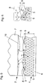
- FIG. 1 illustrated situation, the only part of the chemical reactions occurring during or immediately after the pre-bonding step between a first contact surface 3 of a first substrate 1 and a second contact surface 4 of a second substrate 2.
- the surfaces are terminated with polar OH groups and correspondingly hydrophilic.
- the first substrate 1 and the second substrate 2 are held by the attractive force of the hydrogen bonds between the OH groups present on the surface and the H 2 O molecules as well as between the H 2 O molecules alone.
- the hydrophilicity of at least the first contact surface 3 is increased in a preceding step by a plasma treatment of the first contact surface 3.
- a reservoir 5 has been formed in a surface layer 6 consisting of thermal silicon dioxide.
- the plasma treatment with O 2 ions with ion energies in the range between 0 and 2000 eV has an average thickness R reaches the reservoir 5 of about 15 nm, wherein the ions form channels or pores in the surface layer 6.
- the reservoir 5 is filled with H 2 O as the first starting material.
- the reservoir also contains reduced species of the ions present in the plasma process, in particular O 2 , N 2 , H 2 , Ar.
- the contact surfaces 3, 4 therefore still have a relatively wide distance, in particular due to the existing between the contact surfaces 3, 4 water. Accordingly, the existing bond strength is relatively low and is approximately between 100 mJ / cm 2 and 300 mJ / cm 2 , in particular more than 200 mJ / cm 2 .
- the previous plasma activation plays a decisive role, in particular because of the increased hydrophilicity of the plasma-activated first contact surface 3 and a smoothing effect caused by the plasma activation.
- the in Fig. 1 shown, referred to as Prebond, process can preferably proceed at ambient temperature or a maximum of 50 ° Celsius.
- the Fig. 2a and 2b show a hydrophilic bond, the Si-O-Si bridge with elimination of water by -OH terminated surfaces is achieved.
- the processes in Fig. 2a and 2b last at room temperature about 300h. At 50 ° C about 60h.
- the state in Fig. 2b Does not occur without production of the reservoir at the temperatures mentioned.
- H 2 O molecules are formed which provide at least partially for further filling in the reservoir 5, as far as there is still free space.
- the remaining H 2 O molecules are removed.
- the stage according to FIG. 1 are about 3 to 5 individual layers of OH groups or H 2 O present and the step according to FIG. 1 according to the step FIG. 2a 1 to 3 monolayers of H 2 O are removed or taken up in the reservoir 5.
- Covalent compounds in the form of silanol groups between the contact surfaces 3, 4 are again formed with the deposition of H 2 O molecules according to the reaction shown below, which lead to a significantly stronger bonding force and require less space, so that the distance between the contact surfaces 3, 4 is further reduced until finally the in FIG. 3 shown minimum distance due to the direct meeting of the contact surfaces 3, 4 is achieved: Si-OH + HO-Si ⁇ ⁇ Si-O-Si + H 2 O
- the process step shown is the temperature with preference to a maximum of 500 ° C, with more preference to a maximum of 300 ° C even greater preference to a maximum of 200 ° C, with the greatest preference to a maximum of 100 ° C, with utmost preference not increased above room temperature to a create irreversible or permanent bond between the first and the second contact surface.
- Reservoir 5 is the first starting material for the in FIGS. 5 and 6 reaction shown includes: Si + 2H 2 O ⁇ SiO 2 + 2H 2
- H 2 O molecules diffuse as first starting material from the reservoir 5 to the reaction layer 7.
- This diffusion can take place either via a direct contact of the surface layer 6 and the growth layer 8 formed as oxide layers, or via an / between one of the oxide layers present gap 9, take place.
- silicon dioxide ie a chemical compound having a larger molar volume than pure silicon, is formed as reaction product 10 of the above reaction from the reaction layer 7.
- the silica grows at the interface of the reaction layer 7 with the growth layer 8 and thereby deforms the layer of the growth layer 8 formed as a native oxide in the direction of the gaps 9. Again, H 2 O molecules from the reservoir are needed.
- the above-mentioned reaction of the first starting material (H 2 O) takes place with the second Educt (Si) in the reaction layer 7, as far as a mean distance B between the first contact surface 3 and the reaction layer 7 is as low as possible.
- Decisive is therefore the pretreatment of the first substrate 1 and the selection of the second substrate 2, which consists of a reaction layer 7 made of silicon and a very thin native oxide layer as the growth layer 8.
- a thin as possible native oxide layer is provided according to the invention for two reasons.
- the growth layer 8 is very thin, so that it can bulge out through the newly formed reaction product 10 on the reaction layer 7 formed as an oxide layer surface layer 6 of the opposing substrate 1 out, mainly in areas of the nano-gaps 9. Furthermore, are as short as possible Diffusion paths desirable to achieve the desired effect as quickly as possible and at the lowest possible temperature.
- the first substrate 1 also consists of a silicon layer and an oxide layer formed thereon as the surface layer 6, in which at least partially or completely a reservoir 5 is formed.
- the amount of first starting material required to close the nano-gaps 9 is filled up so that an optimal growth of the growth layer 8 for closing the nano-gaps 9 can take place in the shortest possible time and / or at the lowest possible temperature ,
Description
Die vorliegende Erfindung betrifft ein Verfahren zum Bonden einer ersten Kontaktfläche eines ersten Substrats mit einer zweiten Kontaktfläche eines zweiten Substrats gemäß Patentanspruch 1.The present invention relates to a method for bonding a first contact surface of a first substrate to a second contact surface of a second substrate according to
Ziel beim permanenten oder irreversiblen Bonden von Substraten ist es, zwischen den beiden Kontaktflächen der Substrate eine möglichst starke und insbesondere unwiderrufliche Verbindung, also eine hohe Bondkraft, zu erzeugen. Hierfür existieren im Stand der Technik verschiedene Ansätze und Herstellungsverfahren.The goal of permanent or irreversible bonding of substrates is to create as strong and, in particular, irrevocable connection, ie a high bonding force, between the two contact surfaces of the substrates. For this purpose, various approaches and production methods exist in the prior art.
Die bekannten Herstellungsverfahren und bisher verfolgten Ansätze führen häufig zu nicht oder schlecht reproduzierbaren und insbesondere kaum auf veränderte Bedingungen übertragbaren Ergebnissen. Insbesondere benutzen derzeit eingesetzte Herstellungsverfahren häufig hohe Temperaturen, insbesondere >400°C, um wiederholbare Ergebnisse zu gewährleisten.The known preparation processes and hitherto pursued approaches often lead to no or poorly reproducible and in particular hardly transferable to changing conditions results. In particular, currently used manufacturing processes often use high temperatures, in particular> 400 ° C, to ensure repeatable results.
Technische Probleme wie hoher Energieverbrauch und eine mögliche Zerstörung von auf den Substraten vorhandenen Strukturen resultieren aus den bisher für eine hohe Bondkraft erforderlichen hohen Temperaturen von teilweise weit über 300° C.Technical problems such as high energy consumption and possible destruction of structures present on the substrates result from the high temperatures previously required for a high bonding force, in some cases well above 300 ° C.
Weitere Anforderungen bestehen in:
- der Front-end-of-line-Kompatibilität.
Darunter versteht man die Kompatibilität des Prozesses während der Herstellung der elektrisch aktiven Bauteile. Der Bondingprozess muss also so ausgelegt werden, dass aktive Bauelemente wie Transistoren, die bereits auf den Strukturwafern vorhanden sind, während der Prozessierung weder beeinträchtigt noch geschädigt werden. Zu den Kompatibilitätskriterien zählen vor allem die Reinheit an gewissen chemischen Elementen (vor allem bei CMOS Strukturen), mechanische Belastbarkeit, vor allem durch Thermospannungen. - niedrige Kontamination.
- keine Krafteinbringung.
- the front-end of-line compatibility.
This is the compatibility of the process during the manufacture of the electrically active components. The bonding process must therefore be designed so that active components, such as transistors, which are already present on the structure wafers, are neither affected nor damaged during the processing. The compatibility criteria include above all the purity of certain chemical elements (especially in CMOS structures), mechanical strength, especially by thermal voltages. - low contamination.
- no introduction of force.
Die Reduktion der Bondkraft führt zu einer schonenderen Behandlung der Strukturwafer, und damit zu einer Reduktion der Ausfallswahrscheinlichkeit durch direkte mechanische Belastung.The reduction of the bonding force leads to a gentler treatment of the structure wafers, and thus to a reduction in the probability of failure due to direct mechanical stress.
Die Dokumente
Aufgabe der vorliegenden Erfindung ist es daher, ein Verfahren zur schonenden Herstellung eines permanenten Bonds mit einer möglichst hohen Bondkraft anzugeben.Object of the present invention is therefore to provide a method for the gentle production of a permanent bond with the highest possible bond strength.
Diese Aufgabe wird mit den Merkmalen des Patentanspruchs 1 gelöst. Vorteilhafte Weiterbildungen der Erfindung sind in den Unteransprüchen angegeben. In den Rahmen der Erfindung fallen auch sämtliche Kombinationen aus zumindest zwei von in der Beschreibung, den Ansprüchen und/oder den Figuren angegebenen Merkmalen. Bei angegebenen Wertebereichen sollen auch innerhalb der genannten Grenzen liegende Werte als Grenzwerte offenbart gelten und in beliebiger Kombination beanspruchbar sein.This object is achieved with the features of
Die Grundidee der vorliegenden Erfindung ist es, zumindest an einem der Substrate ein Reservoir zur Aufnahme eines ersten Edukts zu schaffen, das nach der Kontaktierung beziehungsweise Herstellung eines vorläufigen Bonds zwischen den Substraten mit einem zweiten Edukt, das in dem anderen Substrat vorliegt, zu reagieren und dadurch einen irreversiblen beziehungsweise permanenten Bond zwischen den Substraten auszubilden. Vor oder nach der Ausbildung des Reservoirs in einer Oberflächenschicht an der ersten Kontaktfläche findet meist eine Reinigung des oder der Substrate, insbesondere durch einen Spülschritt, statt. Diese Reinigung soll zumeist sicherstellen, dass sich keine Partikel auf den Oberflächen befinden, die ungebondete Stellen zur Folge haben würden. Durch das Reservoir und das im Reservoir enthaltene Edukt wird eine technische Möglichkeit geschaffen, unmittelbar an den Kontaktflächen nach der Herstellung des vorläufigen beziehungsweise reversiblen Bonds gezielt eine den permanenten Bond verstärkende und die Bondgeschwindigkeit erhöhende Reaktion zu induzieren, insbesondere durch Verformung mindestens einer der Kontaktflächen durch die Reaktion, vorzugsweise der dem Reservoir gegenüberliegenden Kontaktfläche.The basic idea of the present invention is to provide a reservoir for receiving a first starting material on at least one of the substrates, which, after the contacting or production of a temporary bond between the substrates, reacts with a second starting material which is present in the other substrate thereby forming an irreversible or permanent bond between the substrates. Before or after the formation of the reservoir in a surface layer on the first contact surface is usually a cleaning of the substrate or, in particular by a rinsing step instead. This cleaning should usually ensure that there are no particles on the surfaces that would result in unbonded areas. By means of the reservoir and the reactant contained in the reservoir, a technical possibility is created to induce directly at the contact surfaces after the preparation of the provisional or reversible bond a permanent bond enhancing and increasing the bond speed reaction, in particular by deformation of at least one of the contact surfaces through the Reaction, preferably the contact surface opposite the reservoir.
Für den Pre-Bonding-Schritt zur Erzeugung eines vorläufigen oder reversiblen Bonds zwischen den Substraten sind verschiedene Möglichkeiten vorgesehen mit dem Ziel, eine schwache Interaktion zwischen den Kontaktflächen der Substrate zu erzeugen. Die Prebondstärken liegen dabei unter den Permanentbondstärken, zumindest um den Faktor 2 bis 3, insbesondere um den Faktor 5, vorzugsweise um den Faktor 15, noch bevorzugter um den Faktor 25.Als Richtgrößen werden die Pre-Bondstärken von reinem, nicht aktiviertem, hydrophilisierten Silizium mit ca. 100mJ/m2 und von reinem, plasmaaktivierten hydrophiliserten Silizium mit ca. 200-300mJ/m2 erwähnt. Die Prebonds zwischen den mit Molekülen benetzten Substraten kommen hauptsächlich durch die van-der-Waals Wechselwirkungen zwischen den Molekülen der unterschiedlichen Waferseiten zustande. Dementsprechend sind vor allem Moleküle mit permanenten Dipolmomenten dafür geeignet, Prebonds zwischen Wafern zu ermöglichen. Als Verbindungsmittel werden folgende chemische Verbindungen beispielhaft, aber nicht einschränkend, genannt
- Wasser,
- Tiole,
- AP3000,
- Silane und/oder
- Silanole
- Water,
- Tiole,
- AP3000,
- Silanes and / or
- silanols
Als erfindungsgemäße Substrate sind solche Substrate geeignet, deren Material in der Lage ist, als Edukt mit einem weiteren zugeführten Edukt zu einem Produkt mit einem höheren molaren Volumen zu reagieren, wodurch die Bildung einer Aufwuchsschicht auf dem Substrat bewirkt wird. Besonders vorteilhaft sind die nachfolgenden Kombinationen, wobei jeweils links vom Pfeil das Edukt und rechts vom Pfeil das Produkt / die Produkte genannt ist, ohne das mit dem Edukt reagierende zugeführte Edukt oder Nebenprodukte im Einzelnen zu benennen:
- Si→SiO2, Si3N4, SiNxOy
- Ge→ GeO2, Ge3N4
- α-Sn→ SnO2
- B→ B2O3, BN
- Se→ SeO2
- Te→ TeO2, TeO3
- Mg→ MgO, Mg3N2
- Al→ Al2O3, AlN
- Ti→ TiO2, TiN
- V→ V2O5
- Mn→ MnO, MnO2, Mn2O3, Mn2O7, Mn3O4
- Fe → FeO, Fe2O3, Fe3O4
- Co→ CoO, Co3O4,
- Ni→ NiO, Ni2O3
- Cu→ CuO CU2O, Cu3N
- Zn→ ZnO
- Cr→ CrN, Cr23C6, Cr3C, Cr7C3, Cr3C2
- Mo→ Mo3C2
- Ti→ TiC
- Nb→ Nb4C3
- Ta→ Ta4C3
- Zr→ ZrC
- Hf→ HfC
- V→ V4C3, VC
- W→ W2C, WC
- Fe→ Fe3C, Fe7C3, Fe2C.
- Si → SiO 2 , Si 3 N 4 , SiN x O y
- Ge → GeO 2 , Ge 3 N 4
- α-Sn → SnO 2
- B → B 2 O 3 , BN
- Se → SeO 2
- Te → TeO 2 , TeO 3
- Mg → MgO, Mg 3 N 2
- Al → Al 2 O 3 , AlN
- Ti → TiO 2 , TiN
- V → V 2 O 5
- Mn → MnO, MnO 2 , Mn 2 O 3 , Mn 2 O 7 , Mn 3 O 4
- Fe → FeO, Fe 2 O 3 , Fe 3 O 4
- Co → CoO, Co 3 O 4 ,
- Ni → NiO, Ni 2 O 3
- Cu → CuO CU 2 O, Cu 3 N
- Zn → ZnO
- Cr → CrN, Cr 23 C 6 , Cr 3 C, Cr 7 C 3 , Cr 3 C 2
- Mo → Mo 3 C 2
- Ti → TiC
- Nb → Nb 4 C 3
- Ta → Ta 4 C 3
- Zr → ZrC
- Hf → HfC
- V → V 4 C 3 , VC
- W → W 2 C, WC
- Fe → Fe 3 C, Fe 7 C 3 , Fe 2 C.
Als Substrate sind außerdem folgende Mischformen von Halbleitern denkbar:
- III-V: GaP, GaAs, InP, InSb, InAs, GaSb, GaN, AlN, InN, AlxGa1. xAs, InxGa1-xN
- IV-IV: SiC, SiGe,
- III-VI: InAlP.
- nichtlineare Optik: LiNbO3, LiTaO3, KDP (KH2PO4)
- Solarzellen: CdS, CdSe, CdTe, CuInSe2, CuInGaSe2, CuInS2, CuInGaS2
- Leitende Oxide: In2-xSnxO3-y
- III-V: GaP, GaAs, InP, InSb, InAs, GaSb, GaN, AlN, InN, Al x Ga 1 . x As, In x Ga 1-x N
- IV-IV: SiC, SiGe,
- III-VI: In ALP.
- nonlinear optics: LiNbO 3 , LiTaO 3 , KDP (KH 2 PO 4 )
- Solar Cells: CdS, CdSe, CdTe, CuInSe 2 , CuInGaSe 2 , CuInS 2 , CuInGaS 2
- Conductive oxides: In 2-x SnxO 3-y
Erfindungsgemäß wird an mindestens einem der Wafer, und zwar unmittelbar an die jeweilige Kontaktfläche ein Reservoir vorgesehen, in welchem eine gewisse Menge mindestens eines der zugeführten Edukte für die Volumenexpansionsreaktion speicherbar ist. Edukte können also beispielsweise O2, O3, H2O, N2, NH3, H2O2 etc. sein. Durch die Expansion, insbesondere bedingt durch Oxidwachstum, werden auf Grund der Bestrebung der Reaktionspartner, die Systemenergie abzusenken, etwaige Lücken, Poren, Hohlräume zwischen den Kontaktflächen minimiert und die Bondkraft entsprechend durch Annäherung der Abstände zwischen den Substraten in diesen Bereichen erhöht. Im bestmöglichen Fall werden die vorhandenen Lücken, Poren und Hohlräume komplett geschlossen, sodass die gesamte Bondingfläche zunimmt und damit die Bondkraft erfindungsgemäß entsprechend steigt.According to the invention, a reservoir is provided on at least one of the wafers, specifically directly to the respective contact surface, in which a certain amount of at least one of the supplied educts can be stored for the volume expansion reaction. Educts can therefore be, for example, O 2 , O 3 , H 2 O, N 2 , NH 3 , H 2 O 2, etc. Due to the expansion, in particular due to oxide growth, due to the efforts of the reaction partners to lower the system energy, any gaps, pores, Minimizes voids between the contact surfaces and increases the bonding force accordingly by approaching the distances between the substrates in these areas. In the best case, the existing gaps, pores and cavities are completely closed, so that the total bonding area increases and thus increases the bonding force according to the invention accordingly.
Die Kontaktflächen zeigen üblicherweise eine Rauhigkeit mit einer quadratischen Rauheit (Rq) von 0,2 nm auf. Dies entspricht Scheitel-ScheitelWerten der Oberflächen im Bereich von 1 nm. Diese empirischen Werte wurden mit der Atomic Force Microscopy (AFM) ermittelt.The contact surfaces usually show a roughness with a roughness (R q ) of 0.2 nm. This corresponds to peak-to-peak values of the surfaces in the range of 1 nm. These empirical values were determined by Atomic Force Microscopy (AFM).
Die erfindungsgemäße Reaktion ist geeignet, bei einer üblichen Waferfläche eines kreisförmigen Wafers mit einem Durchmesser von 200 bis 300 mm mit 1 Monolage (ML) Wasser die Aufwuchsschicht um 0,1 bis 0,3 nm wachsen zu lassen.The reaction according to the invention is suitable for growing the growth layer by 0.1 to 0.3 nm in a conventional wafer surface of a circular wafer having a diameter of 200 to 300 mm with 1 monolayer (ML) of water.
Erfindungsgemäß ist daher insbesondere vorgesehen, mindestens 2 ML, vorzugsweise mindestens 5 ML, noch bevorzugter mindestens 10 ML Fluid, insbesondere Wasser, im Reservoir zu speichern.The invention therefore provides, in particular, for storing at least 2 ml, preferably at least 5 ml, more preferably at least 10 ml of fluid, in particular water, in the reservoir.
Besonders bevorzugt ist die Ausbildung des Reservoirs durch Plasmabeaufschlagung, da durch die Plasmabeaufschlagung außerdem eine Glättung der Kontaktfläche sowie eine Hydrophilisierung als Synergieeffekte bewirkt werden. Die Glättung der Oberfläche durch Plasmaaktivierung erfolgt vorwiegend durch einen viskosen Fluss des Materials der Oberflächenschicht. Die Erhöhung der Hydrophilizität erfolgt insbesondere durch die Vermehrung der Siliziumhydroxyl Verbindungen, vorzugsweise durch Cracken von an der Oberfläche vorhandenen Si-O Verbindungen wie Si-O-Si, insbesondere gemäß nachfolgender Reaktion:
Si-O-Si + H2O ←→ 2SiOH
Particularly preferred is the formation of the reservoir by plasma treatment, since the plasma treatment also a smoothing of the contact surface and a hydrophilization are effected as synergy effects. The smoothing of the surface by plasma activation takes place predominantly by a viscous flow of the material of the surface layer. The increase in the hydrophilicity is effected in particular by the multiplication of the silicon-hydroxyl compounds, preferably by cracking Si-O compounds present on the surface, such as Si-O-Si, in particular according to the following reaction:
Si-O-Si + H 2 O ← → 2SiOH
Ein weiterer Nebeneffekt, insbesondere als Folge der vorgenannten Effekte, besteht darin, dass die Pre-Bond-Stärke, insbesondere um einen Faktor 2 bis 3, verbessert wird.Another side effect, in particular as a result of the aforementioned effects, is that the pre-bond strength, in particular by a factor of 2 to 3, is improved.
Die Ausbildung des Reservoirs in der Oberflächenschicht an der ersten Kontaktfläche des ersten Substrats erfolgt beispielsweise durch Plasmaaktivierung des mit einem thermischen Oxid beschichteten ersten Substrats. Die Plasmaaktivierung wird in einer Vakuumkammer durchgeführt, um die für das Plasma erforderlichen Bedingungen einstellen zu können. Erfindungsgemäß wird für die Plasmaentladung N2-Gas, O2-Gas oder Argongas mit Ionenenergien im Bereich von 0 bis 2000 eV verwendet, wodurch ein Reservoir mit einer Tiefe von bis zu 20 nm, vorzugsweise bis zu 15 nm, mit größerem Vorzug bis zu 10nm, mit größtem Vorzug bis zu 5nm, der behandelten Oberfläche, in diesem Fall der ersten Kontaktfläche, hergestellt wird. Erfindungsgemäß können jede Partikelart, Atome und/oder Moleküle, verwendet werden, die geeignet sind, das Reservoir zu erzeugen. Mit Vorzug werden jene Atome und/oder Moleküle verwendet, welche das Reservoir mit den benötigten Eigenschaften erzeugt. Die relevanten Eigenschaften sind vor allem die Porengröße, Porenverteilung und Porendichte. Alternativ können erfindungsgemäß Gasmischungen, wie beispielsweise Luft oder Formiergas bestehend aus 95% Ar und 5% H2 verwendet werden. Abhängig von dem verwendeten Gas sind in dem Reservoir während der Plasmabehandlung unter anderem folgende Ionen anwesend: N+, N2+, O+, O2+, Ar+. Im nicht belegten Freiraum ist das erste Edukt aufnehmbar.The formation of the reservoir in the surface layer on the first contact surface of the first substrate takes place, for example, by plasma activation of the thermal oxide-coated first substrate. The plasma activation is carried out in a vacuum chamber in order to adjust the conditions required for the plasma. According to the invention, N 2 gas, O 2 gas or argon gas with ion energies in the range of 0 to 2000 eV is used for the plasma discharge, whereby a reservoir with a depth of up to 20 nm, preferably up to 15 nm, more preferably up to 10nm, most preferably up to 5nm, of the treated surface, in this case the first contact surface. Any type of particle, atoms and / or molecules that are suitable for generating the reservoir can be used according to the invention. It is preferred to use those atoms and / or molecules which produce the reservoir with the required properties. The relevant properties are above all the pore size, pore distribution and pore density. Alternatively, according to the invention gas mixtures, such as air or forming gas consisting of 95% Ar and 5% H 2 can be used. Depending on the gas used, among others, the following ions are present in the reservoir during the plasma treatment: N +, N 2 +, O +, O 2 +, Ar +. In the unoccupied free space, the first reactant is absorbable.
Die Ausbildung des Reservoirs erfolgt auf Grund folgender Überlegungen: Die Porengröße ist kleiner als 10nm, mit Vorzug kleiner als 5nm, mit größerem Vorzug kleiner als 1nm, mit noch größerem Vorzug kleiner als 0.5nm, mit größtem Vorzug kleiner als 0.2nm.The formation of the reservoir is based on the following considerations: The pore size is less than 10nm, preferably less than 5nm, more preferably less than 1nm, even more preferably less than 0.5nm, most preferably less than 0.2nm.
Die Porendichte ist mit Vorzug direkt proportional zur Dichte der Partikel, welche die Poren durch Einschlagwirkung erzeugen, mit größtem Vorzug sogar durch den Partialdruck der Einschlagspezies variierbar, sowie abhängig von der Behandlungszeit und den Parametern, insbesondere des verwendeten Plasmasystems.The pore density is preferably directly proportional to the density of the particles which generate the pores by impaction, most preferably even by the partial pressure of the impact species variable, and depending on the treatment time and the parameters, in particular of the plasma system used.
Die Porenverteilung besitzt mit Vorzug mindestens einen Bereich größter Porenkonzentration unter der Oberfläche, durch Variation der Parameter mehrerer solcher Bereiche, welche sich zu einem, vorzugsweise plateauförmigen Bereich, überlagern (siehe
Für die Porengröße, die Porenverteilung und Porendichte gelten für alle nicht mit Plasma hergestellten Verfahren ähnliche Überlegungen.Similar considerations apply to pore size, pore distribution and pore density for all non-plasma processes.
Das Reservoir kann durch gezielte Verwendung und Kombination von Prozessparametern designed werden.
Als Reservoir ist alternativ zu einem durch Plasma erzeugten Reservoir die Verwendung einer TEOS (Tetraethylorthosilikat)-Oxidschicht auf mindestens einem der Substrate, zumindest dem ersten Substrat, denkbar. Dieses Oxid ist im allgemeinen weniger dicht als thermisches Oxid, weshalb erfindungsgemäß eine Verdichtung vorteilhaft ist. Die Verdichtung erfolgt durch Wärmebehandlung mit dem Ziel einer Einstellung einer definierten Porosität des Reservoirs.As a reservoir, the use of a TEOS (tetraethyl orthosilicate) oxide layer on at least one of the substrates, at least the first substrate, is conceivable as an alternative to a plasma-generated reservoir. This oxide is generally less dense than thermal oxide, which is why compaction is advantageous according to the invention. The compaction is carried out by heat treatment with the aim of setting a defined porosity of the reservoir.
Besonders vorteilhaft kann gemäß einer Ausführungsform der Erfindung die Auffüllung des Reservoirs gleichzeitig mit der Ausbildung des Reservoirs erfolgen, indem das Reservoir als Beschichtung auf dem ersten Substrat aufgebracht wird, wobei die Beschichtung das erste Edukt bereits umfasst.Particularly advantageously, according to an embodiment of the invention, the filling of the reservoir can take place simultaneously with the formation of the reservoir by applying the reservoir as a coating on the first substrate, wherein the coating already comprises the first educt.
Das Reservoir ist als poröse Schicht mit einer Porosität im Nanometerbereich oder als Kanäle aufweisende Schicht mit einer Kanaldicke kleiner 10nm, mit größerem Vorzug kleiner als 5 nm, mit noch größerem Vorzug kleiner als 2nm, mit größtem Vorzug kleiner als 1nm, mit allergrößtem Vorzug kleiner als 0.5nm denkbar.The reservoir is a porous layer with a porosity in the nanometer range or as a channel having a channel thickness less than 10nm, more preferably less than 5nm, even more preferably less than 2nm, most preferably less than 1nm, most preferably less than 0.5nm conceivable.
Für den Schritt des Auffüllens des Reservoirs mit dem ersten Edukt oder einer ersten Gruppe von Edukten sind erfindungsgemäß folgende Ausführungsformen, auch in Kombination, denkbar:
- Aussetzen des Reservoirs gegenüber der Umgebungsatmosphäre,
- Spülung mit, insbesondere deionisiertem, Wasser,
- Spülen mit einem das Edukt enthaltenden oder aus diesem bestehenden Fluid, insbesondere H2O, H2O2, NH4OH
- Aussetzen des Reservoirs gegenüber einer beliebigen Gasatmosphäre, insbesondere atomares Gas, molekulares Gas, Gasmischungen,
- Aussetzen des Reservoirs gegenüber einer Wasserdampf oder Wasserstoffperoxiddampf enthaltenden Atmosphäre und
- Ablagerung eines bereits mit dem Edukt befüllten Reservoirs als Oberflächenschicht auf dem ersten Substrat.
- Exposing the reservoir to the ambient atmosphere,
- Rinsing with, in particular deionized, water,
- Rinsing with a fluid containing or consisting of the educt, in particular H 2 O, H 2 O 2 ,
NH 4 OH - Exposing the reservoir to any gas atmosphere, in particular atomic gas, molecular gas, gas mixtures,
- Exposing the reservoir to an atmosphere containing water vapor or hydrogen peroxide vapor and
- Deposit of a reservoir already filled with the educt as a surface layer on the first substrate.
Als Edukte kommen die folgenden Verbindungen in Frage: O2, O3, N2, NH3, H2O, H2O2 und/oder NH4OH.Suitable starting materials are the following compounds: O 2 , O 3 , N 2 , NH 3 , H 2 O, H 2 O 2 and / or NH 4 OH.
Die Verwendung des oben angeführten Wasserstoffperoxiddampfes wird neben der Verwendung von Wasser als bevorzugte Variante angesehen. Wassertstoffperoxid hat des Weiteren den Vorteil, ein größeres Sauerstoff zu Wasserstoffverhältnis zu besitzen. Des Weiteren dissoziiert Wasserstoffperoxid über bestimmten Temperaturen und/oder der Verwendung von Hochfrequenzfeldern im MHz Bereich zu Wasserstoff und Sauerstoff.The use of the above-mentioned hydrogen peroxide vapor is considered to be the preferred variant besides the use of water. Hydrogen peroxide also has the advantage of having a greater oxygen to hydrogen ratio. Furthermore, hydrogen peroxide dissociates into hydrogen and oxygen over certain temperatures and / or the use of radio frequency fields in the MHz range.
Gemäß einer vorteilhaften Ausführungsform der Erfindung ist vorgesehen, dass die Ausbildung der Aufwuchsschicht und Verstärkung des irreversiblen Bonds durch Diffusion des ersten Edukts in die Reaktionsschicht erfolgt.According to an advantageous embodiment of the invention it is provided that the formation of the growth layer and reinforcement of the irreversible bond by diffusion of the first starting material takes place in the reaction layer.
Gemäß einer weiteren, vorteilhaften Ausführungsform der Erfindung ist vorgesehen, dass die Ausbildung des irreversiblen Bonds bei einer Temperatur von typischerweise weniger als 300°C, mit Vorteil von weniger als 200°C, mit größerem Vorzug weniger als 150°C, mit noch größerem Vorzug weniger als 100°C, mit größtem Vorzug bei Raumtemperatur insbesondere während maximal 12 Tage, bevorzugter maximal 1 Tag, noch bevorzugter maximal 1 Stunde, am bevorzugtesten maximal 15 min., erfolgt.According to a further advantageous embodiment of the invention it is provided that the formation of the irreversible bond at a temperature of typically less than 300 ° C, with advantage of less greater than 200 ° C, more preferably less than 150 ° C, even more preferably less than 100 ° C, most preferably at room temperature for a maximum of 12 days, more preferably not more than 1 day, even more preferably not more than 1 hour, most preferably not more than 15 min., takes place.
Dabei ist es besonders vorteilhaft, wenn der irreversible Bond eine Bondstärke von größer 1,5 J/m2; insbesondere größer 2 J/m2, vorzugsweise größer 2,5 J/m2 aufweist.It is particularly advantageous if the irreversible bond has a bond strength of greater than 1.5 J / m 2 ; in particular greater than 2 J / m 2 , preferably greater than 2.5 J / m 2 .
Die Bondstärke kann in besonders vorteilhafter Weise dadurch erhöht werden, dass bei der Reaktion erfindungsgemäß ein Produkt mit einem größeren molaren Volumen als das molare Volumen des zweiten Edukts in der Reaktionsschicht gebildet wird. Hierdurch wird ein Anwachsen am zweiten Substrat bewirkt, wodurch Lücken zwischen den Kontaktflächen durch die erfindungsgemäße chemische Reaktion geschlossen werden können. Als Folge hieraus wird der Abstand zwischen den Kontaktflächen, also der mittlere Abstand, reduziert und Toträume minimiert.The bond strength can be increased in a particularly advantageous manner by virtue of the fact that in the reaction according to the invention a product having a larger molar volume than the molar volume of the second starting material is formed in the reaction layer. As a result, an increase on the second substrate is effected, whereby gaps between the contact surfaces can be closed by the chemical reaction according to the invention. As a result, the distance between the contact surfaces, so the average distance is reduced and minimized dead space.
Soweit die Ausbildung des Reservoirs durch Plasmaaktivierung, insbesondere mit einer Aktivierungsfrequenz zwischen 10 und 600 kHz und/oder einer Leistungsdichte zwischen 0,075 und 0,2 Watt/cm2 und/oder unter Druckbeaufschlagung mit einem Druck zwischen 0,1 und 0,6 mbar, erfolgt, werden zusätzliche Effekte wie die Glättung der Kontaktfläche als auch eine deutlich erhöhte Hydrophilität der Kontaktfläche bewirkt.As far as the formation of the reservoir by plasma activation, in particular with an activation frequency between 10 and 600 kHz and / or a power density between 0.075 and 0.2 watts / cm 2 and / or pressurized with a pressure between 0.1 and 0.6 mbar, takes place, additional effects such as the smoothing of the contact surface as well as a significantly increased hydrophilicity of the contact surface are effected.
Alternativ dazu kann die Ausbildung des Reservoirs erfindungsgemäß durch Verwendung einer, insbesondere kontrolliert auf eine bestimmte Porosität verdichteten, Tetraethoxysilan-Oxidschicht als Oberflächenschicht erfolgen.Alternatively, the formation of the reservoir can be carried out according to the invention by using a tetraethoxysilane oxide layer, in particular controlled to a specific porosity, as a surface layer.
Gemäß einer weiteren vorteilhaften Ausführungsform der Erfindung ist vorgesehen, dass die Oberflächenschicht überwiegend, insbesondere im wesentlichen vollständig, aus einem, insbesondere amorphen, insbesondere einem durch thermische Oxidation erzeugten Siliziumdioxid, und die Reaktionsschicht aus einem oxidierbaren Material, insbesondere überwiegend, vorzugsweise im wesentlichen vollständig, aus Si, Ge, InP, GaP oder GaN, bestehen. Durch Oxidation wird eine besonders stabile und die vorhandenen Lücken besonders effektiv schließende Reaktion ermöglicht.According to a further advantageous embodiment of the invention it is provided that the surface layer predominantly, in particular substantially completely, of one, in particular amorphous, in particular a silicon dioxide produced by thermal oxidation, and the reaction layer of an oxidizable material, in particular predominantly predominantly, preferably substantially completely, of Si, Ge, InP, GaP or GaN. By oxidation, a particularly stable and the existing gaps particularly effective closing reaction allows.
Dabei ist es erfindungsgemäß besonders vorteilhaft, wenn zwischen der zweiten Kontaktfläche und der Reaktionsschicht eine Aufwuchsschicht, insbesondere überwiegend aus nativem Siliziumdioxid, vorgesehen ist. Die Aufwuchsschicht unterliegt einem durch die erfindungsgemäße Reaktion bewirkten Wachstum. Das Wachstum erfolgt ausgehend vom Übergang Si-SiO2 (7) durch Neubildung von amorphem SiO2 und dadurch hervorgerufener Verformung, insbesondere Ausbeulung, der Aufwuchsschicht, nisbesondere an der Grenzfläche zur Reaktionsschicht, und zwar insbesondere in Bereichen von Lücken zwischen der ersten und der zweiten Kontaktfläche. Hierdurch wird eine Reduzierung des Abstands beziehungsweise Verringerung des Totraums zwischen den beiden Kontaktflächen bewirkt, wodurch die Bondstärke zwischen den beiden Substraten erhöht wird. Besonders vorteilhaft ist dabei eine Temperatur zwischen 200 und 400°C, bevorzugt in etwa 200°C und 150° C, bevorzugterweise eine Temperatur zwischen 150°C und 100°C, am bevorzugtesten eine Temperatur zwischen 100°C und Raumtemperatur.In this case, it is particularly advantageous according to the invention if a growth layer, in particular predominantly of native silicon dioxide, is provided between the second contact surface and the reaction layer. The growth layer is subject to growth caused by the reaction of the present invention. The growth takes place starting from the transition Si-SiO 2 (7) by new formation of
Hierbei ist es besonders vorteilhaft, wenn die Aufwuchsschicht vor der Ausbildung des irreversiblen Bonds eine mittlere Dicke A zwischen 0,1 nm und 5 nm aufweist. Je dünner die Aufwuchsschicht, desto schneller und einfacher erfolgt die Reaktion zwischen dem ersten und dem zweiten Edukt durch die Aufwuchsschicht hindurch, insbesondere durch Diffusion des ersten Edukts durch die Aufwuchsschicht hindurch zur Reaktionsschicht.In this case, it is particularly advantageous if the growth layer has an average thickness A between 0.1 nm and 5 nm before the formation of the irreversible bond. The thinner the growth layer, the faster and easier the reaction between the first and the second educt takes place through the growth layer, in particular by diffusion of the first starting material through the growth layer to the reaction layer.
In vorteilhafter Weise ist gemäß einer Ausführungsform der Erfindung vorgesehen, dass die Ausbildung des Reservoirs im Vakuum durchgeführt wird. Somit können Verunreinigungen des Reservoirs mit nicht erwünschten Materialien oder Verbindungen vermieden werden.Advantageously, it is provided according to an embodiment of the invention that the formation of the reservoir carried out in a vacuum becomes. Thus, contamination of the reservoir with undesirable materials or compounds can be avoided.
In einer weiteren Ausführungsform der Erfindung ist mit Vorteil vorgesehen, dass das Auffüllen des Reservoirs durch einen oder mehrere der nachfolgend aufgeführten Schritte erfolgt:
- Aussetzen der ersten Kontaktfläche gegenüber der Atmosphäre, zur Auffüllung des Reservoirs mit Luftfeuchtigkeit und / oder in der Luft enthaltenem Sauerstoff.
- Beaufschlagung der ersten Kontaktfläche mit einem, insbesondere überwiegend, vorzugsweise nahezu vollständig, aus, insbesondere deionisiertem, H2O und/oder H2O2 bestehenden, Fluid,
- Beaufschlagung der ersten Kontaktfläche mit N2-Gas und/oder O2-Gas und/oder Ar-Gas und/oder Formiergas, insbesondere bestehend aus 95% Ar und 5% H2, insbesondere mit einer Ionenenergie
im Bereich von 0 bis 2000 eV. - Bedampfung zur Auffüllung des Reservoirs mit einem beliebigen bereits genannten Edukt.
- Exposing the first contact surface to the atmosphere, filling the reservoir with humidity and / or oxygen contained in the air.
- Acting on the first contact surface with a, in particular predominantly, preferably almost completely, of, in particular deionized, H 2 O and / or H 2 O 2 existing fluid,
- Acting on the first contact surface with N 2 gas and / or O 2 gas and / or Ar gas and / or forming gas, in particular consisting of 95% Ar and 5% H 2 , in particular with an ion energy in the range of 0 to 2000 eV ,
- Steaming to fill the reservoir with any educt already mentioned.
Besonders effektiv für den Verfahrensablauf ist es, wenn das Reservoir mit Vorzug in einer Dicke R zwischen 0,1 nm und 25 nm, mit größerem Vorzug zwischen 0,1 nm und 15 nm, mit noch größerem Vrozug zwischen 0,1 nm und 10 nm, mit größtem Vorzug zwischen 0,1 nm und 5 nm ausgebildet wird. Weiterhin ist es gemäß einer Ausführungsform der Erfindung vorteilhaft, wenn der mittlere Abstand B zwischen dem Reservoir und der Reaktionsschicht unmittelbar vor der Ausbildung des irreversiblen Bonds zwischen 0,1 nm und 15 nm, insbesondere zwischen 0,5 nm und 5 nm, vorzugsweise zwischen 0,5 nm und 3 nm beträgt.It is particularly effective for the process sequence if the reservoir is preferably in a thickness R between 0.1 nm and 25 nm, more preferably between 0.1 nm and 15 nm, with even greater volume between 0.1 nm and 10 nm , is formed with the greatest preference between 0.1 nm and 5 nm. Furthermore, according to one embodiment of the invention, it is advantageous if the mean distance B between the reservoir and the reaction layer immediately before the formation of the irreversible bond between 0.1 nm and 15 nm, in particular between 0.5 nm and 5 nm, preferably between 0.5 nm and 3 nm.
Eine Vorrichtung zur Ausführung des Verfahrens ist erfindungsgemäß mit einer Kammer zur Ausbildung des Reservoirs und einer, insbesondere separat dazu vorgesehenen Kammer zur Füllung des Reservoirs und einer, insbesondere separat vorgesehenen Kammer zur Ausbildung des Pre-Bonds ausgebildet, die direkt über ein Vakuumsystem miteinander verbunden sind.A device for carrying out the method according to the invention is formed with a chamber for forming the reservoir and a, in particular separately provided chamber for filling the reservoir and a, in particular separately provided chamber for forming the pre-bond, which are directly connected to each other via a vacuum system ,
In einer weiteren Ausführungsform kann das Auffüllen des Reservoirs auch direkt über die Atmosphäre erfolgen, also entweder in einer Kammer, die zur Atmosphäre hin geöffnet werden kann oder einfach auf einem Aufbau, welcher keine Ummantelung besitzt aber den Wafer semi- und/oder vollautomatisch handhaben kann.In a further embodiment, the filling of the reservoir can also be carried out directly via the atmosphere, ie either in a chamber which can be opened to the atmosphere or simply on a structure which has no sheathing but can handle the wafer semi-automatically and / or fully automatically ,
Weitere Vorteile, Merkmale und Einzelheiten der Erfindung ergeben sich aus der nachfolgenden Beschreibung bevorzugter Ausführungsbeispiele sowie anhand der Zeichnungen. Diese zeigen in:
Figur 1- einen ersten Schritt des erfindungsgemäßen Verfahrens unmittelbar nach der Kontaktierung des ersten Substrats mit dem zweiten Substrat,
- Figur 2a und 2b
- weitere Schritte des erfindungsgemäßen Verfahrens zur Ausbildung einer höheren Bondstärke,
Figur 3- einen sich an die
Schritte gemäß Figur 1, Figur 2a und Figur 2b anschließender weiterer Schritt des erfindungsgemäßen Verfahrens mit in Kontakt stehenden Kontaktflächen der Substrate, Figur 4- einen erfindungsgemäßen Schritt zur Ausbildung eines irreversiblen/permanenten Bonds zwischen den Substraten,
Figur 5- eine vergrößerte Darstellung der an den beiden Kontaktflächen während der Schritte gemäß
Figur 3 und Figur 4 ablaufenden chemischen/physikalischen Vorgängen, Figur 6- eine weiter vergrößerte Darstellung der an der Grenzfläche zwischen den beiden Kontaktflächen ablaufenden chemischen/physikalischen Vorgänge während der Schritte gemäß
Figur 3 und Figur 4 und Figur 7- ein Diagramm zur erfindungsgemäßen Erzeugung des Reservoirs.
- FIG. 1
- a first step of the method according to the invention immediately after the contacting of the first substrate with the second substrate,
- FIGS. 2a and 2b
- further steps of the method according to the invention for forming a higher bond strength,
- FIG. 3
- Follow the steps according to
Figure 1, Figure 2a and Figure 2b subsequent further step of the method according to the invention with contact surfaces of the substrates in contact, - FIG. 4
- a step according to the invention for forming an irreversible / permanent bond between the substrates,
- FIG. 5
- an enlarged view of the two contact surfaces during the steps according to
FIG. 3 and FIG. 4 ongoing chemical / physical processes, - FIG. 6
- a further enlarged view of the running at the interface between the two contact surfaces chemical / physical processes during the steps according to
FIG. 3 and FIG. 4 and - FIG. 7
- a diagram for the generation of the reservoir according to the invention.
In den Figuren sind gleiche oder gleichwirkende Merkmale mit den gleichen Bezugszeichen gekennzeichnet.In the figures, identical or equivalent features are identified by the same reference numerals.
In der in
Durch die Plasmabehandlung ist erfindungsgemäß ein Reservoir 5 in einer aus thermischem Siliziumdioxid bestehenden Oberflächenschicht 6 ausgebildet worden. Durch die Plasmabehandlung mit O2-Ionen mit Ionenenergien im Bereich zwischen 0 und 2000 eV wird eine mittlere Dicke R des Reservoirs 5 von etwa 15 nm erreicht, wobei die Ionen Kanäle beziehungsweise Poren in der Oberflächenschicht 6 ausbilden.By means of the plasma treatment, according to the invention, a
Ebenfalls vor dem in
Die Kontaktflächen 3, 4 weisen daher noch einen relativ weiten Abstand auf, insbesondere bedingt durch das zwischen den Kontaktflächen 3, 4 vorhandene Wasser. Entsprechend ist die vorhandene Bondstärke relativ gering und liegt etwa zwischen 100 mJ/cm2 und 300 mJ/cm2, insbesondere über 200 mJ/cm2. Hierbei spielt die vorherige Plasmaaktivierung, insbesondere wegen der erhöhten Hydrophilizität der plasmaaktivierten ersten Kontaktfläche 3 sowie einem durch die Plasmaaktivierung verursachten Glättungseffekt, eine entscheidende Rolle.The contact surfaces 3, 4 therefore still have a relatively wide distance, in particular due to the existing between the contact surfaces 3, 4 water. Accordingly, the existing bond strength is relatively low and is approximately between 100 mJ / cm 2 and 300 mJ / cm 2 , in particular more than 200 mJ / cm 2 . Here, the previous plasma activation plays a decisive role, in particular because of the increased hydrophilicity of the plasma-activated
Der in
Zwischen den Kontaktflächen 3, 4 werden H2O-Moleküle gebildet, die zumindest teilweise für eine weitere Auffüllung im Reservoir 5 sorgen, soweit noch Freiraum vorhanden ist. Die übrigen H2O-Moleküle werden entfernt. In der Stufe gemäß
In dem in
In dem in
Si-OH + HO-Si ←→ Si-O-Si+H2O
In the in
Si-OH + HO-Si ← → Si-O-Si + H 2 O
Bis zur Stufe 3 ist es, insbesondere wegen der Schaffung des Reservoirs 5, nicht notwendig, die Temperatur übermäßig zu erhöhen, eher sogar bei Raumtemperatur ablaufen zu lassen. Auf diese Weise ist ein besonders schonender Ablauf der Verfahrensschritte gemäß
In dem in
Si + 2H2O → SiO2 + 2H2
In the in
Si + 2H 2 O → SiO 2 + 2H 2
Bei den obengenanten, leicht erhöhten Temperaturen diffundieren H2O-Moleküle als erstes Edukt von dem Reservoir 5 zur Reaktionsschicht 7. Diese Diffusion kann entweder über einen Direktkontakt der als Oxidschichten ausgebildeten Oberflächenschicht 6 und Aufwuchsschicht 8, oder über eine/aus einer zwischen den Oxidschichten vorliegende Lücke 9, erfolgen. Dort wird Siliziumdioxid, also eine chemische Verbindung mit einem größeren molaren Volumen als reines Silizium, als Reaktionsprodukt 10 der obigen Reaktion aus der Reaktionsschicht 7 gebildet. Das Siliziumdioxid wächst an der Grenzfläche der Reaktionsschicht 7 mit der Aufwuchsschicht 8 und verformt dadurch die Schicht der als natives Oxid ausgebildeten Aufwuchsschicht 8, in Richtung der Lücken 9 aus. Auch hierbei werden H2O-Moleküle aus dem Reservoir benötigt.At the above-mentioned, slightly elevated temperatures, H 2 O molecules diffuse as first starting material from the
Durch die Existenz der Lücken, die im Nanometerbereich liegen, besteht die Möglichkeit des Ausbeulens der nativen Oxidschicht 8, wodurch Spannungen an den Kontaktflächen 3, 4 reduziert werden können. Hierdurch wird der Abstand zwischen den Kontaktflächen 3, 4 reduziert, wodurch sich die wirksame Kontaktfläche und damit die Bondstärke weiter erhöht. Die so zustande gekommene, sich über den gesamten Wafer ausbildende, alle Poren verschließende, Schweißverbindung trägt, im Gegensatz zu den partiell nicht verschweißten Produkten im Stand der Technik, fundamental zur Erhöhung der Bondkraft bei. Der Bindungstyp zwischen beiden miteinander verschweißten amorphen Siliziumoxidoberflächen ist eine Mischform aus kovalentem und ionischem Anteil sein.Due to the existence of the gaps, which are in the nanometer range, there is the possibility of buckling of the
Besonders schnell beziehungsweise bei möglichst niedrigen Temperaturen erfolgt die oben genannte Reaktion des ersten Edukts (H2O) mit dem zweiten Edukt (Si) in der Reaktionsschicht 7, soweit ein mittlerer Abstand B zwischen der ersten Kontaktfläche 3 und der Reaktionsschicht 7 möglichst gering ist.Particularly fast or at temperatures as low as possible, the above-mentioned reaction of the first starting material (H 2 O) takes place with the second Educt (Si) in the
Entscheidend ist daher die Vorbehandlung des ersten Substrats 1 sowie die Auswahl des zweiten Substrats 2, das aus einer Reaktionsschicht 7 aus Silizium und einer möglichst dünnen nativen Oxidschicht als Aufwuchsschicht 8 besteht. Eine möglichst dünne native Oxidschicht ist aus zwei Gründen erfindungsgemäß vorgesehen. Die Aufwuchsschicht 8 ist sehr dünn, damit sie sich durch das neu gebildete Reaktionsprodukt 10 an der Reaktionsschicht 7 zur als Oxidschicht ausgebildeten Oberflächenschicht 6 des gegenüberliegenden Substrats 1 hin ausbeulen kann, und zwar vorwiegend in Bereichen der Nano-Lücken 9. Des Weiteren sind möglichst kurze Diffusionswege erwünscht, um den erwünschten Effekt möglichst rasch und bei möglichst niedriger Temperatur zu erzielen. Das erste Substrat 1 besteht ebenfalls aus einer Siliziumschicht und einer darauf erzeugten Oxidschicht als Oberflächenschicht 6, in der zumindest teilweise oder vollständig ein Reservoir 5 ausgebildet wird.Decisive is therefore the pretreatment of the
In dem Reservoir 5 werden erfindungsgemäß mindestens entsprechend der zum Schließen der Nano-Lücken 9 erforderliche Menge an erstem Edukt aufgefüllt, damit ein optimales Aufwachsen der Aufwuchsschicht 8 zum Schließen der Nano-Lücken 9 in möglichst kurzer Zeit und/oder bei möglichst geringer Temperatur erfolgen kann.In the
- 11
- erstes Substratfirst substrate
- 22
- zweites Substratsecond substrate
- 33
- erste Kontaktflächefirst contact surface
- 44
- zweite Kontaktflächesecond contact surface
- 55
- Reservoirreservoir
- 66
- Oberflächenschichtsurface layer
- 77
- Reaktionsschichtreaction layer
- 88th
- Aufwuchsschichtgrew up layer
- 99
- Nano-LückenNano-gaps
- 1010
- Reaktionsproduktreaction product
- 1111
- Erstes ProfilFirst profile
- 1212
- Zweites ProfilSecond profile
- 1313
- Summenkurvecumulative curve
- AA
- mittlere Dickeaverage thickness
- BB
- mittlerer Abstandaverage distance
- RR
- mittlere Dickeaverage thickness
Claims (14)
- Method for bonding of a first contact surface (3) of a first substrate (1) to a second contact surface (4) of a second substrate (2) with the following steps, especially the following sequence:- forming a reservoir (5) in a surface layer (6) on the first contact surface (3), wherein the reservoir (5) is formed by plasma activation, wherein reduced species of the ions present in the plasma process are located in the reservoir,- at least partial filling of the reservoir (5) with a first educt or a first group of educts,- contacting the first contact surface (3) with the second contact surface (4) for formation of a prebond connection,- forming a permanent bond between the first and second contact surface (3, 4), at least partially strengthened by the reaction of the first educt with a second educt contained in a reaction layer (7) of the second substrate (2).
- Method as claimed in Claim 1, wherein formation and/or strengthening of the permanent bond takes place by diffusion of the first educt into the reaction layer (7).
- Method as claimed in one of the preceding claims, wherein the formation of the permanent bond takes place at a temperature between room temperature and 200° Celsius, especially during a maximum 12 days, more preferably a maximum 1 day, even more preferably a maximum 1 hour, and most preferably a maximum 15 minutes.
- Method as claimed in one of the preceding claims, wherein the irreversible bond has a bond strength of greater than 1.5 J/m2, especially greater than 2 J/m2, preferably greater than 2.5 J/m2.
- Method as claimed in one of the preceding claims, wherein during the reaction a reaction product (10) with a greater molar volume than the molar volume of the second educts is formed in the reaction layer (7).
- Method as claimed in claim 1, wherein the reduced species are O2-, N2-, H2-, Ar-ions.
- Method as claimed in one of the preceding claims, wherein the surface layer (6) consists predominantly, especially essentially completely of an especially amorphous, especially silicon oxide produced by thermal oxidation, and the reaction layer (7) consists of an oxidizable material, especially predominantly, preferably essentially completely, of Si, Ge, InP, GaP or GaN.
- Method as claimed in one of the preceding claims, wherein between the second contact surface (4) and the reaction layer (7) there is a growth layer (8), especially predominantly of native silicon dioxide.
- Method as claimed in Claim 8, wherein before formation of a permanent bond the growth layer (8) has an average thickness A between 1 angstrom and 10 nm.
- Method as claimed in one of the preceding claims, wherein a reservoir is formed in a vacuum.
- Method as claimed in one of the preceding claims, wherein the reservoir is filled by one or more of the steps cited below:- exposing the first contact surface (3) to the atmosphere, especially with a high oxygen and/or water content,- exposing the first contact surface (3) to a fluid consisting especially predominantly, preferably almost completely, of especially deionized H2O and/or H2O2,- exposing the first contact surface (3) to N2 gas and/or O2 gas and/or Ar gas and/or forming gas, especially consisting of 95% Ar and 5% H2, especially with an ion energy in the range from 0 to 2000 eV.
- Method as claimed in one of the preceding claims, wherein the reservoir (5) is formed in an average thickness (R) between 0.1 nm and 25 nm, especially between 0.1 nm and 20 nm.
- Method as claimed in one of the preceding claims, wherein the average distance (B) between the reservoir (5) and the reaction layer (7) immediately before formation of the permanent bond is between 0.1 nm and 15 nm, especially between 0.5 nm and 5 nm, preferably between 0.5 nm and 3 nm.
- Method as claimed in one of the preceding claims, wherein the irreversible bond has a bond strength which comprises 2 times, preferably 4 times, more preferably 10 times, most preferably 25 times the prebond strength.
Priority Applications (3)
| Application Number | Priority Date | Filing Date | Title |
|---|---|---|---|
| EP15197291.6A EP3024014B9 (en) | 2011-01-25 | 2011-01-25 | Method for the permanent bonding of wafers |
| EP18196480.0A EP3447789B1 (en) | 2011-01-25 | 2011-01-25 | Method for the permanent bonding of wafers |
| EP18196492.5A EP3442006A3 (en) | 2011-01-25 | 2011-01-25 | Method for the permanent bonding of wafers |
Applications Claiming Priority (3)
| Application Number | Priority Date | Filing Date | Title |
|---|---|---|---|
| EP15197291.6A EP3024014B9 (en) | 2011-01-25 | 2011-01-25 | Method for the permanent bonding of wafers |
| PCT/EP2011/000299 WO2012100786A1 (en) | 2011-01-25 | 2011-01-25 | Method for the permanent bonding of wafers |
| EP11702931.4A EP2668661B1 (en) | 2011-01-25 | 2011-01-25 | Method for the permanent bonding of wafers |
Related Parent Applications (2)
| Application Number | Title | Priority Date | Filing Date |
|---|---|---|---|
| EP11702931.4A Division EP2668661B1 (en) | 2011-01-25 | 2011-01-25 | Method for the permanent bonding of wafers |
| EP11702931.4A Division-Into EP2668661B1 (en) | 2011-01-25 | 2011-01-25 | Method for the permanent bonding of wafers |
Related Child Applications (4)
| Application Number | Title | Priority Date | Filing Date |
|---|---|---|---|
| EP18196492.5A Division-Into EP3442006A3 (en) | 2011-01-25 | 2011-01-25 | Method for the permanent bonding of wafers |
| EP18196492.5A Division EP3442006A3 (en) | 2011-01-25 | 2011-01-25 | Method for the permanent bonding of wafers |
| EP18196480.0A Division EP3447789B1 (en) | 2011-01-25 | 2011-01-25 | Method for the permanent bonding of wafers |
| EP18196480.0A Division-Into EP3447789B1 (en) | 2011-01-25 | 2011-01-25 | Method for the permanent bonding of wafers |
Publications (3)
| Publication Number | Publication Date |
|---|---|
| EP3024014A1 EP3024014A1 (en) | 2016-05-25 |
| EP3024014B1 true EP3024014B1 (en) | 2018-11-28 |
| EP3024014B9 EP3024014B9 (en) | 2019-04-24 |
Family
ID=44510564
Family Applications (4)
| Application Number | Title | Priority Date | Filing Date |
|---|---|---|---|
| EP11702931.4A Active EP2668661B1 (en) | 2011-01-25 | 2011-01-25 | Method for the permanent bonding of wafers |
| EP18196480.0A Active EP3447789B1 (en) | 2011-01-25 | 2011-01-25 | Method for the permanent bonding of wafers |
| EP18196492.5A Ceased EP3442006A3 (en) | 2011-01-25 | 2011-01-25 | Method for the permanent bonding of wafers |
| EP15197291.6A Active EP3024014B9 (en) | 2011-01-25 | 2011-01-25 | Method for the permanent bonding of wafers |
Family Applications Before (3)
| Application Number | Title | Priority Date | Filing Date |
|---|---|---|---|
| EP11702931.4A Active EP2668661B1 (en) | 2011-01-25 | 2011-01-25 | Method for the permanent bonding of wafers |
| EP18196480.0A Active EP3447789B1 (en) | 2011-01-25 | 2011-01-25 | Method for the permanent bonding of wafers |
| EP18196492.5A Ceased EP3442006A3 (en) | 2011-01-25 | 2011-01-25 | Method for the permanent bonding of wafers |
Country Status (8)
| Country | Link |
|---|---|
| US (3) | US9252042B2 (en) |
| EP (4) | EP2668661B1 (en) |
| JP (1) | JP5955866B2 (en) |
| KR (6) | KR101705937B1 (en) |
| CN (3) | CN103329247B (en) |
| SG (1) | SG192102A1 (en) |
| TW (5) | TWI681438B (en) |
| WO (1) | WO2012100786A1 (en) |
Families Citing this family (13)
| Publication number | Priority date | Publication date | Assignee | Title |
|---|---|---|---|---|
| US9252042B2 (en) | 2011-01-25 | 2016-02-02 | Ev Group E. Thallner Gmbh | Method for permanent bonding of wafers |
| SG192180A1 (en) | 2011-04-08 | 2013-08-30 | Ev Group E Thallner Gmbh | Method for permanent bonding of wafer |
| WO2013029656A1 (en) * | 2011-08-30 | 2013-03-07 | Ev Group E. Thallner Gmbh | Method for permanently bonding wafers by a connecting layer by means of solid-state diffusion or phase transformation |
| FR3001225B1 (en) * | 2013-01-22 | 2016-01-22 | Commissariat Energie Atomique | METHOD FOR MANUFACTURING DIRECT COLLAGE STRUCTURE |
| CN110310896B (en) * | 2013-07-05 | 2023-08-15 | Ev 集团 E·索尔纳有限责任公司 | Method for joining contact surfaces of substrates |
| JP6379184B2 (en) * | 2013-09-25 | 2018-08-22 | エーファウ・グループ・エー・タルナー・ゲーエムベーハー | Apparatus and method for bonding substrates |
| DE102014112430A1 (en) | 2014-08-29 | 2016-03-03 | Ev Group E. Thallner Gmbh | Method for producing a conductive multi-substrate stack |
| JP2016171307A (en) * | 2015-03-10 | 2016-09-23 | 株式会社デンソー | Substrate bonding method |
| JP6106239B2 (en) * | 2015-09-30 | 2017-03-29 | エーファウ・グループ・エー・タルナー・ゲーエムベーハー | Method for permanently bonding a wafer |
| US10084090B2 (en) * | 2015-11-09 | 2018-09-25 | International Business Machines Corporation | Method and structure of stacked FinFET |
| FR3045939B1 (en) * | 2015-12-22 | 2018-03-30 | Commissariat A L'energie Atomique Et Aux Energies Alternatives | METHOD FOR DIRECT COLLAGE BETWEEN TWO STRUCTURES |
| US10373830B2 (en) * | 2016-03-08 | 2019-08-06 | Ostendo Technologies, Inc. | Apparatus and methods to remove unbonded areas within bonded substrates using localized electromagnetic wave annealing |
| KR102624841B1 (en) | 2017-03-02 | 2024-01-15 | 에베 그룹 에. 탈너 게엠베하 | Method and device for bonding chips |
Family Cites Families (65)
| Publication number | Priority date | Publication date | Assignee | Title |
|---|---|---|---|---|
| US545154A (en) * | 1895-08-27 | colbuen | ||
| JPS62211390A (en) * | 1986-03-12 | 1987-09-17 | Hitachi Ltd | Ceramic coated heat resistant member and its production |
| DE3942964A1 (en) | 1989-12-23 | 1991-06-27 | Leybold Ag | DEVICE FOR PRODUCING A PLASMA |
| US5451547A (en) | 1991-08-26 | 1995-09-19 | Nippondenso Co., Ltd. | Method of manufacturing semiconductor substrate |
| JP3191371B2 (en) | 1991-12-11 | 2001-07-23 | ソニー株式会社 | Semiconductor wafer bonding method |
| US5427638A (en) | 1992-06-04 | 1995-06-27 | Alliedsignal Inc. | Low temperature reaction bonding |
| JP3192000B2 (en) | 1992-08-25 | 2001-07-23 | キヤノン株式会社 | Semiconductor substrate and manufacturing method thereof |
| EP1018153A1 (en) * | 1997-08-29 | 2000-07-12 | Sharon N. Farrens | In situ plasma wafer bonding method |
| KR100311234B1 (en) | 1999-01-18 | 2001-11-02 | 학교법인 인하학원 | Enhanced inductively coupled plasma reactor |
| US20020048900A1 (en) | 1999-11-23 | 2002-04-25 | Nova Crystals, Inc. | Method for joining wafers at a low temperature and low stress |
| US6902987B1 (en) * | 2000-02-16 | 2005-06-07 | Ziptronix, Inc. | Method for low temperature bonding and bonded structure |
| JP2004515053A (en) | 2000-06-26 | 2004-05-20 | アプライド マテリアルズ インコーポレイテッド | Wafer cleaning method and apparatus |
| US6563133B1 (en) | 2000-08-09 | 2003-05-13 | Ziptronix, Inc. | Method of epitaxial-like wafer bonding at low temperature and bonded structure |
| JP4759821B2 (en) * | 2001-03-08 | 2011-08-31 | ソニー株式会社 | Manufacturing method of semiconductor device |
| US6780759B2 (en) | 2001-05-09 | 2004-08-24 | Silicon Genesis Corporation | Method for multi-frequency bonding |
| US6814833B2 (en) * | 2001-10-26 | 2004-11-09 | Corning Incorporated | Direct bonding of articles containing silicon |
| US20030089950A1 (en) | 2001-11-15 | 2003-05-15 | Kuech Thomas F. | Bonding of silicon and silicon-germanium to insulating substrates |
| JPWO2003046993A1 (en) * | 2001-11-29 | 2005-04-14 | 信越半導体株式会社 | Manufacturing method of SOI wafer |
| US6962835B2 (en) * | 2003-02-07 | 2005-11-08 | Ziptronix, Inc. | Method for room temperature metal direct bonding |
| FR2851846A1 (en) | 2003-02-28 | 2004-09-03 | Canon Kk | CONNECTION SYSTEM AND METHOD FOR MANUFACTURING SEMICONDUCTOR SUBSTRATE |
| US7109092B2 (en) * | 2003-05-19 | 2006-09-19 | Ziptronix, Inc. | Method of room temperature covalent bonding |
| JP3980539B2 (en) | 2003-08-29 | 2007-09-26 | 唯知 須賀 | Substrate bonding method, irradiation method, and substrate bonding apparatus |
| JP4118774B2 (en) * | 2003-09-18 | 2008-07-16 | 株式会社東芝 | Thin film laminate and manufacturing method thereof |
| US7740737B2 (en) | 2004-06-21 | 2010-06-22 | Tokyo Electron Limited | Plasma processing apparatus and method |
| EP1621565A1 (en) | 2004-07-28 | 2006-02-01 | Cytec Surface Specialties Austria GmbH | Epoxy resins with improved elasticity |
| US7261793B2 (en) | 2004-08-13 | 2007-08-28 | Hewlett-Packard Development Company, L.P. | System and method for low temperature plasma-enhanced bonding |
| US7148122B2 (en) * | 2004-08-24 | 2006-12-12 | Intel Corporation | Bonding of substrates |
| JP2006080314A (en) | 2004-09-09 | 2006-03-23 | Canon Inc | Manufacturing method of coupled substrate |
| EP1792337B1 (en) * | 2004-09-21 | 2010-05-26 | S.O.I.Tec Silicon on Insulator Technologies | Transfer method with a treatment of a surface to be bonded |
| US8138061B2 (en) * | 2005-01-07 | 2012-03-20 | International Business Machines Corporation | Quasi-hydrophobic Si-Si wafer bonding using hydrophilic Si surfaces and dissolution of interfacial bonding oxide |
| US7772088B2 (en) | 2005-02-28 | 2010-08-10 | Silicon Genesis Corporation | Method for manufacturing devices on a multi-layered substrate utilizing a stiffening backing substrate |
| FR2884966B1 (en) | 2005-04-22 | 2007-08-17 | Soitec Silicon On Insulator | METHOD OF BONDING TWO SLICES REALIZED IN MATERIALS SELECTED AMONG SEMICONDUCTOR MATERIALS |
| JP5166690B2 (en) | 2005-06-02 | 2013-03-21 | 三菱重工業株式会社 | Solid polymer electrolyte fuel cell |
| FR2888663B1 (en) | 2005-07-13 | 2008-04-18 | Soitec Silicon On Insulator | METHOD OF REDUCING THE ROUGHNESS OF A THICK LAYER OF INSULATION |
| US7601271B2 (en) | 2005-11-28 | 2009-10-13 | S.O.I.Tec Silicon On Insulator Technologies | Process and equipment for bonding by molecular adhesion |
| TWI261316B (en) * | 2005-12-28 | 2006-09-01 | Ind Tech Res Inst | Wafer bonding method |
| US7923353B2 (en) * | 2006-03-27 | 2011-04-12 | Okmetic Oyj | Gettering method and a wafer using the same |
| US7579654B2 (en) * | 2006-05-31 | 2009-08-25 | Corning Incorporated | Semiconductor on insulator structure made using radiation annealing |
| JP2008005230A (en) * | 2006-06-22 | 2008-01-10 | Sony Corp | Circuit for processing video signal, video display device and method for processing video signal |
| KR100748723B1 (en) * | 2006-07-10 | 2007-08-13 | 삼성전자주식회사 | Bonding method of substrates |
| US7745309B2 (en) | 2006-08-09 | 2010-06-29 | Applied Materials, Inc. | Methods for surface activation by plasma immersion ion implantation process utilized in silicon-on-insulator structure |
| EP1928020B1 (en) * | 2006-11-30 | 2020-04-22 | Soitec | Method of manufacturing a semiconductor heterostructure |
| US7939387B2 (en) | 2007-03-19 | 2011-05-10 | S.O.I.Tec Silicon On Insulator Technologies | Patterned thin SOI |
| CN101652867B (en) * | 2007-04-06 | 2012-08-08 | 株式会社半导体能源研究所 | Photovoltaic device and method for manufacturing the same |
| JP5183969B2 (en) * | 2007-05-29 | 2013-04-17 | 信越半導体株式会社 | Method for forming silicon oxide film on SOI wafer |
| US20090061593A1 (en) * | 2007-08-28 | 2009-03-05 | Kishor Purushottam Gadkaree | Semiconductor Wafer Re-Use in an Exfoliation Process Using Heat Treatment |
| JP5499428B2 (en) | 2007-09-07 | 2014-05-21 | 株式会社Sumco | Manufacturing method of bonded wafer |
| US8101501B2 (en) | 2007-10-10 | 2012-01-24 | Semiconductor Energy Laboratory Co., Ltd. | Method of manufacturing semiconductor device |
| EP2075830A3 (en) * | 2007-10-11 | 2011-01-19 | Sumco Corporation | Method for producing bonded wafer |
| FR2923079B1 (en) | 2007-10-26 | 2017-10-27 | S O I Tec Silicon On Insulator Tech | SUBSTRATES SOI WITH INSULATED FINE LAYER ENTERREE |
| JP5465830B2 (en) * | 2007-11-27 | 2014-04-09 | 信越化学工業株式会社 | Manufacturing method of bonded substrate |
| US20090139963A1 (en) | 2007-11-30 | 2009-06-04 | Theodoros Panagopoulos | Multiple frequency pulsing of multiple coil source to control plasma ion density radial distribution |
| KR101250057B1 (en) * | 2008-02-08 | 2013-04-03 | 도쿄엘렉트론가부시키가이샤 | Method for modifying insulating film with plasma |
| CN101261932A (en) | 2008-04-18 | 2008-09-10 | 华中科技大学 | A bonding method for low-temperature round slice |
| JP5552276B2 (en) | 2008-08-01 | 2014-07-16 | 株式会社半導体エネルギー研究所 | Method for manufacturing SOI substrate |
| US7927975B2 (en) | 2009-02-04 | 2011-04-19 | Micron Technology, Inc. | Semiconductor material manufacture |
| GB0919830D0 (en) | 2009-11-12 | 2009-12-30 | Isis Innovation | Preparation of silicon for fast generation of hydrogen through reaction with water |
| US9252042B2 (en) | 2011-01-25 | 2016-02-02 | Ev Group E. Thallner Gmbh | Method for permanent bonding of wafers |
| US8975158B2 (en) | 2011-04-08 | 2015-03-10 | Ev Group E. Thallner Gmbh | Method for permanently bonding wafers |
| SG192180A1 (en) | 2011-04-08 | 2013-08-30 | Ev Group E Thallner Gmbh | Method for permanent bonding of wafer |
| WO2012136266A1 (en) | 2011-04-08 | 2012-10-11 | Ev Group E. Thallner Gmbh | Method for permanently bonding wafers |
| EP2511694A1 (en) | 2011-04-15 | 2012-10-17 | Aisapack Holding SA | Device and method for detecting and/or determining the position of a barrier layer made in the wall of a tube-shaped package |
| FR2980916B1 (en) | 2011-10-03 | 2014-03-28 | Soitec Silicon On Insulator | PROCESS FOR PRODUCING A SILICON TYPE STRUCTURE ON INSULATION |
| US8748885B2 (en) | 2012-02-10 | 2014-06-10 | Taiwan Semiconductor Manufacturing Company, Ltd. | Soft material wafer bonding and method of bonding |
| JP6099744B2 (en) | 2012-07-24 | 2017-03-22 | エーファウ・グループ・エー・タルナー・ゲーエムベーハー | Method and apparatus for continuously bonding wafers |
-
2011
- 2011-01-25 US US13/981,353 patent/US9252042B2/en active Active
- 2011-01-25 EP EP11702931.4A patent/EP2668661B1/en active Active
- 2011-01-25 JP JP2013549719A patent/JP5955866B2/en active Active
- 2011-01-25 EP EP18196480.0A patent/EP3447789B1/en active Active
- 2011-01-25 EP EP18196492.5A patent/EP3442006A3/en not_active Ceased
- 2011-01-25 EP EP15197291.6A patent/EP3024014B9/en active Active
- 2011-01-25 KR KR1020137017302A patent/KR101705937B1/en active IP Right Grant
- 2011-01-25 WO PCT/EP2011/000299 patent/WO2012100786A1/en active Application Filing
- 2011-01-25 KR KR1020217006520A patent/KR102353489B1/en active IP Right Grant
- 2011-01-25 KR KR1020227001508A patent/KR102430673B1/en active IP Right Grant
- 2011-01-25 KR KR1020207008326A patent/KR102225764B1/en active IP Right Grant
- 2011-01-25 SG SG2013056189A patent/SG192102A1/en unknown
- 2011-01-25 KR KR1020177035566A patent/KR102095095B1/en active IP Right Grant
- 2011-01-25 CN CN201180065964.9A patent/CN103329247B/en active Active
- 2011-01-25 CN CN201810607031.1A patent/CN108682623B/en active Active
- 2011-01-25 CN CN201810604777.7A patent/CN108766873B/en active Active
- 2011-01-25 KR KR1020157034723A patent/KR101810310B1/en active IP Right Grant
-
2012
- 2012-01-20 TW TW104143011A patent/TWI681438B/en active
- 2012-01-20 TW TW101102642A patent/TWI594292B/en active
- 2012-01-20 TW TW108112376A patent/TWI699820B/en active
- 2012-01-20 TW TW107119559A patent/TWI660399B/en active
- 2012-01-20 TW TW108112375A patent/TWI697939B/en active
-
2015
- 2015-12-21 US US14/976,484 patent/US10083933B2/en active Active
-
2018
- 2018-08-21 US US16/106,326 patent/US20190006313A1/en not_active Abandoned
Non-Patent Citations (1)
| Title |
|---|
| None * |
Also Published As
Similar Documents
| Publication | Publication Date | Title |
|---|---|---|
| EP3024014B1 (en) | Method for the permanent bonding of wafers | |
| EP2695182B1 (en) | Method for permanently bonding wafers | |
| EP2878006B9 (en) | Method and device for permanently bonding wafers | |
| EP2695181B1 (en) | Method for permanently bonding wafers | |
| EP2695183A1 (en) | Method for permanently bonding wafers | |
| DE102004030612B3 (en) | Semiconductor substrate and method for its production | |
| JP2014510418A5 (en) | ||
| DE112008000394T5 (en) | A method of manufacturing a substrate comprising a deposited buried oxide layer | |
| EP2847786B1 (en) | Method for bonding substrates | |
| JP2020065090A (en) | Wafer permanent bonding method | |
| JP6679666B2 (en) | Wafer permanent bonding method | |
| JP6106239B2 (en) | Method for permanently bonding a wafer |
Legal Events
| Date | Code | Title | Description |
|---|---|---|---|
| AC | Divisional application: reference to earlier application |
Ref document number: 2668661 Country of ref document: EP Kind code of ref document: P |
|
| AK | Designated contracting states |
Kind code of ref document: A1 Designated state(s): AL AT BE BG CH CY CZ DE DK EE ES FI FR GB GR HR HU IE IS IT LI LT LU LV MC MK MT NL NO PL PT RO RS SE SI SK SM TR |
|
| PUAI | Public reference made under article 153(3) epc to a published international application that has entered the european phase |
Free format text: ORIGINAL CODE: 0009012 |
|
| STAA | Information on the status of an ep patent application or granted ep patent |
Free format text: STATUS: REQUEST FOR EXAMINATION WAS MADE |
|
| 17P | Request for examination filed |
Effective date: 20161116 |
|
| RBV | Designated contracting states (corrected) |
Designated state(s): AL AT BE BG CH CY CZ DE DK EE ES FI FR GB GR HR HU IE IS IT LI LT LU LV MC MK MT NL NO PL PT RO RS SE SI SK SM TR |
|
| RIC1 | Information provided on ipc code assigned before grant |
Ipc: H01L 21/762 20060101ALI20180523BHEP Ipc: H01L 23/00 20060101ALI20180523BHEP Ipc: H01L 21/20 20060101ALI20180523BHEP Ipc: H01L 21/70 20060101ALI20180523BHEP Ipc: H01L 21/18 20060101AFI20180523BHEP |
|
| GRAP | Despatch of communication of intention to grant a patent |
Free format text: ORIGINAL CODE: EPIDOSNIGR1 |
|
| STAA | Information on the status of an ep patent application or granted ep patent |
Free format text: STATUS: GRANT OF PATENT IS INTENDED |
|
| INTG | Intention to grant announced |
Effective date: 20180629 |
|
| GRAS | Grant fee paid |
Free format text: ORIGINAL CODE: EPIDOSNIGR3 |
|
| GRAA | (expected) grant |
Free format text: ORIGINAL CODE: 0009210 |
|
| STAA | Information on the status of an ep patent application or granted ep patent |
Free format text: STATUS: THE PATENT HAS BEEN GRANTED |
|
| AC | Divisional application: reference to earlier application |
Ref document number: 2668661 Country of ref document: EP Kind code of ref document: P |
|
| AK | Designated contracting states |
Kind code of ref document: B1 Designated state(s): AL AT BE BG CH CY CZ DE DK EE ES FI FR GB GR HR HU IE IS IT LI LT LU LV MC MK MT NL NO PL PT RO RS SE SI SK SM TR |
|
| REG | Reference to a national code |
Ref country code: CH Ref legal event code: EP |
|
| REG | Reference to a national code |
Ref country code: AT Ref legal event code: REF Ref document number: 1071210 Country of ref document: AT Kind code of ref document: T Effective date: 20181215 |
|
| REG | Reference to a national code |
Ref country code: DE Ref legal event code: R096 Ref document number: 502011015101 Country of ref document: DE |
|
| REG | Reference to a national code |
Ref country code: IE Ref legal event code: FG4D Free format text: LANGUAGE OF EP DOCUMENT: GERMAN |
|
| REG | Reference to a national code |
Ref country code: CH Ref legal event code: PK Free format text: BERICHTIGUNG B9 |
|
| REG | Reference to a national code |
Ref country code: NL Ref legal event code: MP Effective date: 20181128 |
|
| REG | Reference to a national code |
Ref country code: LT Ref legal event code: MG4D |
|
| PG25 | Lapsed in a contracting state [announced via postgrant information from national office to epo] |
Ref country code: HR Free format text: LAPSE BECAUSE OF FAILURE TO SUBMIT A TRANSLATION OF THE DESCRIPTION OR TO PAY THE FEE WITHIN THE PRESCRIBED TIME-LIMIT Effective date: 20181128 Ref country code: NO Free format text: LAPSE BECAUSE OF FAILURE TO SUBMIT A TRANSLATION OF THE DESCRIPTION OR TO PAY THE FEE WITHIN THE PRESCRIBED TIME-LIMIT Effective date: 20190228 Ref country code: BG Free format text: LAPSE BECAUSE OF FAILURE TO SUBMIT A TRANSLATION OF THE DESCRIPTION OR TO PAY THE FEE WITHIN THE PRESCRIBED TIME-LIMIT Effective date: 20190228 Ref country code: LT Free format text: LAPSE BECAUSE OF FAILURE TO SUBMIT A TRANSLATION OF THE DESCRIPTION OR TO PAY THE FEE WITHIN THE PRESCRIBED TIME-LIMIT Effective date: 20181128 Ref country code: FI Free format text: LAPSE BECAUSE OF FAILURE TO SUBMIT A TRANSLATION OF THE DESCRIPTION OR TO PAY THE FEE WITHIN THE PRESCRIBED TIME-LIMIT Effective date: 20181128 Ref country code: IS Free format text: LAPSE BECAUSE OF FAILURE TO SUBMIT A TRANSLATION OF THE DESCRIPTION OR TO PAY THE FEE WITHIN THE PRESCRIBED TIME-LIMIT Effective date: 20190328 Ref country code: ES Free format text: LAPSE BECAUSE OF FAILURE TO SUBMIT A TRANSLATION OF THE DESCRIPTION OR TO PAY THE FEE WITHIN THE PRESCRIBED TIME-LIMIT Effective date: 20181128 Ref country code: LV Free format text: LAPSE BECAUSE OF FAILURE TO SUBMIT A TRANSLATION OF THE DESCRIPTION OR TO PAY THE FEE WITHIN THE PRESCRIBED TIME-LIMIT Effective date: 20181128 |
|
| PG25 | Lapsed in a contracting state [announced via postgrant information from national office to epo] |
Ref country code: SE Free format text: LAPSE BECAUSE OF FAILURE TO SUBMIT A TRANSLATION OF THE DESCRIPTION OR TO PAY THE FEE WITHIN THE PRESCRIBED TIME-LIMIT Effective date: 20181128 Ref country code: AL Free format text: LAPSE BECAUSE OF FAILURE TO SUBMIT A TRANSLATION OF THE DESCRIPTION OR TO PAY THE FEE WITHIN THE PRESCRIBED TIME-LIMIT Effective date: 20181128 Ref country code: RS Free format text: LAPSE BECAUSE OF FAILURE TO SUBMIT A TRANSLATION OF THE DESCRIPTION OR TO PAY THE FEE WITHIN THE PRESCRIBED TIME-LIMIT Effective date: 20181128 Ref country code: PT Free format text: LAPSE BECAUSE OF FAILURE TO SUBMIT A TRANSLATION OF THE DESCRIPTION OR TO PAY THE FEE WITHIN THE PRESCRIBED TIME-LIMIT Effective date: 20190328 Ref country code: GR Free format text: LAPSE BECAUSE OF FAILURE TO SUBMIT A TRANSLATION OF THE DESCRIPTION OR TO PAY THE FEE WITHIN THE PRESCRIBED TIME-LIMIT Effective date: 20190301 |
|
| PG25 | Lapsed in a contracting state [announced via postgrant information from national office to epo] |
Ref country code: NL Free format text: LAPSE BECAUSE OF FAILURE TO SUBMIT A TRANSLATION OF THE DESCRIPTION OR TO PAY THE FEE WITHIN THE PRESCRIBED TIME-LIMIT Effective date: 20181128 |
|
| PG25 | Lapsed in a contracting state [announced via postgrant information from national office to epo] |
Ref country code: PL Free format text: LAPSE BECAUSE OF FAILURE TO SUBMIT A TRANSLATION OF THE DESCRIPTION OR TO PAY THE FEE WITHIN THE PRESCRIBED TIME-LIMIT Effective date: 20181128 Ref country code: DK Free format text: LAPSE BECAUSE OF FAILURE TO SUBMIT A TRANSLATION OF THE DESCRIPTION OR TO PAY THE FEE WITHIN THE PRESCRIBED TIME-LIMIT Effective date: 20181128 Ref country code: CZ Free format text: LAPSE BECAUSE OF FAILURE TO SUBMIT A TRANSLATION OF THE DESCRIPTION OR TO PAY THE FEE WITHIN THE PRESCRIBED TIME-LIMIT Effective date: 20181128 Ref country code: IT Free format text: LAPSE BECAUSE OF FAILURE TO SUBMIT A TRANSLATION OF THE DESCRIPTION OR TO PAY THE FEE WITHIN THE PRESCRIBED TIME-LIMIT Effective date: 20181128 |
|
| REG | Reference to a national code |
Ref country code: DE Ref legal event code: R097 Ref document number: 502011015101 Country of ref document: DE |
|
| PG25 | Lapsed in a contracting state [announced via postgrant information from national office to epo] |
Ref country code: RO Free format text: LAPSE BECAUSE OF FAILURE TO SUBMIT A TRANSLATION OF THE DESCRIPTION OR TO PAY THE FEE WITHIN THE PRESCRIBED TIME-LIMIT Effective date: 20181128 Ref country code: SM Free format text: LAPSE BECAUSE OF FAILURE TO SUBMIT A TRANSLATION OF THE DESCRIPTION OR TO PAY THE FEE WITHIN THE PRESCRIBED TIME-LIMIT Effective date: 20181128 Ref country code: EE Free format text: LAPSE BECAUSE OF FAILURE TO SUBMIT A TRANSLATION OF THE DESCRIPTION OR TO PAY THE FEE WITHIN THE PRESCRIBED TIME-LIMIT Effective date: 20181128 Ref country code: MC Free format text: LAPSE BECAUSE OF FAILURE TO SUBMIT A TRANSLATION OF THE DESCRIPTION OR TO PAY THE FEE WITHIN THE PRESCRIBED TIME-LIMIT Effective date: 20181128 Ref country code: SK Free format text: LAPSE BECAUSE OF FAILURE TO SUBMIT A TRANSLATION OF THE DESCRIPTION OR TO PAY THE FEE WITHIN THE PRESCRIBED TIME-LIMIT Effective date: 20181128 |
|
| REG | Reference to a national code |
Ref country code: CH Ref legal event code: PL |
|
| PG25 | Lapsed in a contracting state [announced via postgrant information from national office to epo] |
Ref country code: LU Free format text: LAPSE BECAUSE OF NON-PAYMENT OF DUE FEES Effective date: 20190125 |
|
| PLBE | No opposition filed within time limit |
Free format text: ORIGINAL CODE: 0009261 |
|
| STAA | Information on the status of an ep patent application or granted ep patent |
Free format text: STATUS: NO OPPOSITION FILED WITHIN TIME LIMIT |
|
| REG | Reference to a national code |
Ref country code: BE Ref legal event code: MM Effective date: 20190131 |
|
| REG | Reference to a national code |
Ref country code: IE Ref legal event code: MM4A |
|
| PG25 | Lapsed in a contracting state [announced via postgrant information from national office to epo] |
Ref country code: SI Free format text: LAPSE BECAUSE OF FAILURE TO SUBMIT A TRANSLATION OF THE DESCRIPTION OR TO PAY THE FEE WITHIN THE PRESCRIBED TIME-LIMIT Effective date: 20181128 |
|
| 26N | No opposition filed |
Effective date: 20190829 |
|
| PG25 | Lapsed in a contracting state [announced via postgrant information from national office to epo] |
Ref country code: BE Free format text: LAPSE BECAUSE OF NON-PAYMENT OF DUE FEES Effective date: 20190131 |
|
| PG25 | Lapsed in a contracting state [announced via postgrant information from national office to epo] |
Ref country code: LI Free format text: LAPSE BECAUSE OF NON-PAYMENT OF DUE FEES Effective date: 20190131 Ref country code: CH Free format text: LAPSE BECAUSE OF NON-PAYMENT OF DUE FEES Effective date: 20190131 |
|
| PG25 | Lapsed in a contracting state [announced via postgrant information from national office to epo] |
Ref country code: IE Free format text: LAPSE BECAUSE OF NON-PAYMENT OF DUE FEES Effective date: 20190125 |
|
| PG25 | Lapsed in a contracting state [announced via postgrant information from national office to epo] |
Ref country code: TR Free format text: LAPSE BECAUSE OF FAILURE TO SUBMIT A TRANSLATION OF THE DESCRIPTION OR TO PAY THE FEE WITHIN THE PRESCRIBED TIME-LIMIT Effective date: 20181128 |
|
| PG25 | Lapsed in a contracting state [announced via postgrant information from national office to epo] |
Ref country code: MT Free format text: LAPSE BECAUSE OF FAILURE TO SUBMIT A TRANSLATION OF THE DESCRIPTION OR TO PAY THE FEE WITHIN THE PRESCRIBED TIME-LIMIT Effective date: 20181128 |
|
| PG25 | Lapsed in a contracting state [announced via postgrant information from national office to epo] |
Ref country code: CY Free format text: LAPSE BECAUSE OF FAILURE TO SUBMIT A TRANSLATION OF THE DESCRIPTION OR TO PAY THE FEE WITHIN THE PRESCRIBED TIME-LIMIT Effective date: 20181128 |
|
| PG25 | Lapsed in a contracting state [announced via postgrant information from national office to epo] |
Ref country code: HU Free format text: LAPSE BECAUSE OF FAILURE TO SUBMIT A TRANSLATION OF THE DESCRIPTION OR TO PAY THE FEE WITHIN THE PRESCRIBED TIME-LIMIT; INVALID AB INITIO Effective date: 20110125 |
|
| PG25 | Lapsed in a contracting state [announced via postgrant information from national office to epo] |
Ref country code: MK Free format text: LAPSE BECAUSE OF FAILURE TO SUBMIT A TRANSLATION OF THE DESCRIPTION OR TO PAY THE FEE WITHIN THE PRESCRIBED TIME-LIMIT Effective date: 20181128 |
|
| PGFP | Annual fee paid to national office [announced via postgrant information from national office to epo] |
Ref country code: FR Payment date: 20230123 Year of fee payment: 13 Ref country code: AT Payment date: 20230118 Year of fee payment: 13 |
|
| PGFP | Annual fee paid to national office [announced via postgrant information from national office to epo] |
Ref country code: GB Payment date: 20230105 Year of fee payment: 13 Ref country code: DE Payment date: 20230123 Year of fee payment: 13 |