EP3016138A1 - Packaged assembly for high density power applications - Google Patents
Packaged assembly for high density power applications Download PDFInfo
- Publication number
- EP3016138A1 EP3016138A1 EP15189330.2A EP15189330A EP3016138A1 EP 3016138 A1 EP3016138 A1 EP 3016138A1 EP 15189330 A EP15189330 A EP 15189330A EP 3016138 A1 EP3016138 A1 EP 3016138A1
- Authority
- EP
- European Patent Office
- Prior art keywords
- double
- sided substrate
- packaged assembly
- case
- substrate
- Prior art date
- Legal status (The legal status is an assumption and is not a legal conclusion. Google has not performed a legal analysis and makes no representation as to the accuracy of the status listed.)
- Granted
Links
Images


Classifications
-
- H—ELECTRICITY
- H10—SEMICONDUCTOR DEVICES; ELECTRIC SOLID-STATE DEVICES NOT OTHERWISE PROVIDED FOR
- H10W—GENERIC PACKAGES, INTERCONNECTIONS, CONNECTORS OR OTHER CONSTRUCTIONAL DETAILS OF DEVICES COVERED BY CLASS H10
- H10W70/00—Package substrates; Interposers; Redistribution layers [RDL]
- H10W70/60—Insulating or insulated package substrates; Interposers; Redistribution layers
- H10W70/62—Insulating or insulated package substrates; Interposers; Redistribution layers characterised by their interconnections
- H10W70/65—Shapes or dispositions of interconnections
-
- H—ELECTRICITY
- H05—ELECTRIC TECHNIQUES NOT OTHERWISE PROVIDED FOR
- H05K—PRINTED CIRCUITS; CASINGS OR CONSTRUCTIONAL DETAILS OF ELECTRIC APPARATUS; MANUFACTURE OF ASSEMBLAGES OF ELECTRICAL COMPONENTS
- H05K1/00—Printed circuits
- H05K1/18—Printed circuits structurally associated with non-printed electric components
- H05K1/181—Printed circuits structurally associated with non-printed electric components associated with surface mounted components
-
- H—ELECTRICITY
- H10—SEMICONDUCTOR DEVICES; ELECTRIC SOLID-STATE DEVICES NOT OTHERWISE PROVIDED FOR
- H10W—GENERIC PACKAGES, INTERCONNECTIONS, CONNECTORS OR OTHER CONSTRUCTIONAL DETAILS OF DEVICES COVERED BY CLASS H10
- H10W70/00—Package substrates; Interposers; Redistribution layers [RDL]
- H10W70/40—Leadframes
- H10W70/479—Leadframes on or in insulating or insulated package substrates, interposers, or redistribution layers
-
- H—ELECTRICITY
- H10—SEMICONDUCTOR DEVICES; ELECTRIC SOLID-STATE DEVICES NOT OTHERWISE PROVIDED FOR
- H10W—GENERIC PACKAGES, INTERCONNECTIONS, CONNECTORS OR OTHER CONSTRUCTIONAL DETAILS OF DEVICES COVERED BY CLASS H10
- H10W70/00—Package substrates; Interposers; Redistribution layers [RDL]
- H10W70/60—Insulating or insulated package substrates; Interposers; Redistribution layers
- H10W70/62—Insulating or insulated package substrates; Interposers; Redistribution layers characterised by their interconnections
- H10W70/63—Vias, e.g. via plugs
- H10W70/635—Through-vias
-
- H—ELECTRICITY
- H10—SEMICONDUCTOR DEVICES; ELECTRIC SOLID-STATE DEVICES NOT OTHERWISE PROVIDED FOR
- H10W—GENERIC PACKAGES, INTERCONNECTIONS, CONNECTORS OR OTHER CONSTRUCTIONAL DETAILS OF DEVICES COVERED BY CLASS H10
- H10W76/00—Containers; Fillings or auxiliary members therefor; Seals
- H10W76/10—Containers or parts thereof
- H10W76/12—Containers or parts thereof characterised by their shape
- H10W76/161—Containers comprising no base
-
- H—ELECTRICITY
- H10—SEMICONDUCTOR DEVICES; ELECTRIC SOLID-STATE DEVICES NOT OTHERWISE PROVIDED FOR
- H10W—GENERIC PACKAGES, INTERCONNECTIONS, CONNECTORS OR OTHER CONSTRUCTIONAL DETAILS OF DEVICES COVERED BY CLASS H10
- H10W90/00—Package configurations
- H10W90/701—Package configurations characterised by the relative positions of pads or connectors relative to package parts
Definitions
- Semiconductor power modules control electrical power to circuits and devices, such as motors, actuators, controllers or the like.
- circuits and devices such as motors, actuators, controllers or the like.
- CTE coefficient of thermal expansion
- a substrate is attached to a package using hardware and hard soldering paste, which add weight to the packaged assembly.
- the contact points between the hardware and the substrate consume the limited usable area of the substrate.
- CTE coefficient of thermal expansion
- the present disclosure is directed to a packaged assembly for high density power applications, substantially as shown in and/or described in connection with at least one of the figures, and as set forth in the claims.
- Figure 1A illustrates a perspective view of a portion of a packaged assembly, according to one implementation of the present application.
- packaged assembly 180 includes case 100, double-sided substrate 120 disposed in case 100, and leads 114 electrically coupled to semiconductor devices and/or circuit elements formed on double-sided substrate 120 through lead frames 112 for external connection.
- leads 114 electrically coupled to semiconductor devices and/or circuit elements formed on double-sided substrate 120 through lead frames 112 for external connection.
- a hermetic lid and an encapsulating molding compound or gap filler are omitted from Figure 1A for purposes of clarity, but may be included in packaged assembly 180.
- case 100 includes a hermetic lid (not explicitly shown in Figure 1A ), walls 102a, 102b, 102c and 102d, a shelf (not explicitly shown in Figure 1A ) on each of opposing walls 102a and 102b for holding and providing support for double-sided substrate 120, and a bottom plate (not explicitly shown in Figure 1A ).
- Case 100 includes a material with low mass, high thermal conductivity and high machinability.
- case 100 includes aluminum silicon (AlSi). The high thermal conductivity of AlSi facilitates transferring heat generated by circuit elements and power semiconductor devices on double-sided substrate 120 out of packaged assembly 180.
- case 100 having AlSi is super lightweight, thereby substantially reducing the overall weight of packaged assembly 180.
- AlSi is highly machinable, which means that the manufacturing process of case 100 (e.g., cutting, removing portions thereof and obtaining a good finish) requires little power and time. With high machinability, it is also easy and quick to make configuration changes to accommodate different footprints of different substrates if needed.
- case 100 may include other suitable material with low mass, high thermal conductivity and high machinability.
- the CTE of case 100 is closely matched with double-sided substrate 120, such that a change in volume (e.g., expansion or contraction) of case 100 in response to a change in temperature does not introduce stress to double-sided substrate 120 or locations in packaged assembly where an epoxy is used to secure double-sided substrate 120 to case 100.
- additional hardware and hard soldering paste are not required to secure double-sided substrate 120 in place, thereby further reducing the overall weight of packaged assembly 180.
- double-sided substrate 120 includes a front side (not explicitly shown in Figure 1A ) and a back side (e.g., back side 122b).
- back side 122b of double-sided substrate 120 includes various circuit elements formed thereon.
- toroidal inductors 104a and 104b, ceramic capacitor stacks 108a, 108b and 108c, tantalum capacitors 110a and 110b and various other circuit elements are formed on back side 122b of double-sided substrate 120.
- Toroidal inductors 104a and 104b each include a circular ring shaped magnetic core around which a strip of wire is wound.
- Toroidal inductors 104a and 104b are configured to filter and reduce noise in the circuitry formed on double-sided substrate 120, for example.
- Tantalum capacitors 110a and 110b are configured to reduce an output noise of a point of load converter formed on double-sided substrate 120, for example.
- Ceramic capacitor stacks 108a, 108b and 108c are also formed on back side 122b of double-sided substrate 120, and configured to filter an input noise of the point of load converter formed on double-sided substrate 120, for example.
- leads 114 extend through walls 102c and 102d of case 100, and are electrically coupled to power semiconductor devices and/or circuit elements formed on double-sided substrate 120 through lead frames 112 along walls 102c and 102d of case 100.
- leads 114 are invertible leads that can be inverted 180° from their current positions as shown in Figure 1A , such that both the hermetic lid and bottom plate 116 of case 100 can be used as a mounting surface for packaged assembly 180.
- leads 114 are made of copper-based metal matrix composite alloys mixed with aluminum, oxide and/or ceramic particles.
- Leads 114 each have a diameter of approximately 30 mils (i.e., one thirty thousandth of an inch), thus allowing for greater current carrying capability and mechanical strength to accommodate power semiconductor devices in packaged assembly 180.
- leads 114 may be made of other conductive materials, and have a diameter of greater or less than 30 mils.
- a hermetic lid (not explicitly shown in Figure 1A ) may be laser welded to case 100 to hermetically seal double-sided substrate 120 in packaged assembly 180.
- an encapsulating molding compound or gap filler may partially or entirely fill the space between circuit elements formed on back side 122b of double-sided substrate 120 and the lid, such that hermetically sealed packaged assembly 180 can withstand g-forces of 5000g or more.
- Figure 1B illustrates a perspective view of a portion of a packaged assembly, according to one implementation of the present application.
- Figure 1B is a perspective view of packaged assembly 180 along line B-B in Figure 1A .
- packaged assembly 180 includes case 100, double-sided substrate 120 disposed on shelf 106a on wall 102a and shelf 106b on wall 102b of case 100, respectively.
- a hermetic lid, an encapsulating molding compound or gap filler, and wall 102d in Figure 1A are omitted from Figure 1B for purposes of clarity, but may be included in packaged assembly 180.
- case 100 includes walls 102a, 102b and 102c, shelves 106a and 106b on respective opposing walls 102a and 102b of case 100, and bottom plate 116.
- shelves 106a and 106b are formed on opposing walls 102a and 102b, respectively, as part of case 100 for providing support for double-sided substrate 120.
- shelves are not formed on walls 102c and 102d since shelves 106a and 106b on respective opposing walls 102a and 102b are sufficient to provide support for double-sided substrate 120.
- additional hardware is not required to secure double-sided substrate 120 to case 100, thereby substantially reducing the overall weight of packaged assembly 180.
- shelves 106a and 106b may be formed by removing one or more portions of case 100 through a machine process.
- shelves 106a and 106b may be formed removing a portion of case 100 by grinding case 100 from a top surface to depth 103 to form upper portions of walls 102a, 102b, 102c and 102d of case 100, then removing another portion of case 100 below depth 103 leaving a narrower width between opposing walls 102a and 102b to form a step on respective lower portions of each of walls 102a and 102b.
- width 107a of shelf 106a is greater than width 109a of the upper portion of wall 102a.
- width 107b of shelf 106b is greater than width 109b of the upper portion of wall 102b. Since shelves 106a and 106b support double-sided substrate 120 at its edges, the contact area between double-sided substrate 120 and case 100 is minimized, thereby allowing more circuit elements and semiconductor devices to be built on both sides of double-sided substrate 120. As such, a high density substrate can be formed. Height 105a of shelf 106a is equal to height 105b of shelf 106b such that double-sided substrate 120 can be situated above and substantially parallel with bottom plate 116. Heights 105a and 105b may be of any appropriate value to provide sufficient clearance for semiconductor dies and circuit elements formed on front side 122a of double-sided substrate 120.
- double-sided substrate 120 is a thick film substrate made of beryllium oxide (BeO) or aluminum oxide (Al 2 O 3 ). In other implementations, double-sided substrate 120 may include other suitable dielectric material.
- double-sided substrate 120 is a single substrate, such as a PC board, which allows one or more semiconductor dies and circuit elements to be attached to both sides of the substrate. By using both sides of a single substrate, for example, of uniform composition, double-sided substrate 120 does not require wafer bonding steps to bond two substrates together, for example, using copper, thereby reducing manufacturing complexity and cost.
- packaged assembly 180 can be a hybrid assembly having bare semiconductor dies and packaged integrated circuits directly attached thereto.
- double-sided substrate 120 includes toroidal inductors 104a and 104b, ceramic capacitor stacks 108a, 108b and 108c, tantalum capacitors 110a and 110b and other circuit elements are formed on back side 122b of double-sided substrate 120.
- double-sided substrate 120 also includes various circuit elements formed on front side 122a of double-sided substrate 120. In contrast to conventional assemblies where only one side of a substrate is used for receive circuit elements and semiconductor devices, implementations of the present application can double the usable area to which semiconductor dies and circuit elements can be attached, through the utilization of both front side 122a and back side 122b of double-sided substrate 120.
- leads 114 extend through wall 102c of case 100, and are electrically coupled to semiconductor devices and/or circuit elements formed on double-sided substrate 120 through lead frames 112 along wall 102c of case 100. In one implementation, leads 114 may be soldered to lead frames 112.
- an epoxy may be applied and cured to perimeters 130a and 130b (as shown in Figure 1B ) along walls 102a and 102b respectively, to secure double-sided substrate 120 to case 100.
- the epoxy may include any suitable material, such as commercially available ME7155 by AI Tech.
- case 100 includes AlSi.
- Double-sided substrate 120 may include a material (e.g., Al 2 O 3 or BeO) having a CTE closely matched with that of case 100.
- a change in volume (e.g., expansion or contraction) of case 100 in response to a change in temperature does not introduce stress to double-sided substrate 120 or perimeters 130a and 130b where the epoxy is applied and cured to secure double-sided substrate 120 to case 100.
- additional hardware and hard soldering paste are not required to secure double-sided substrate 120 in place, thereby substantially reducing the overall weight of packaged assembly 180.
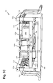
- Figure 1C illustrates a perspective view of a portion of a packaged assembly, according to one implementation of the present application.
- Figure 1C is a perspective view of packaged assembly 180 along line C-C in Figure 1A .
- packaged assembly 180 includes case 100 and double-sided substrate 120 having through substrate vias 124a and 124b extending from front side 122a to back side 122b of double-sided substrate 120.
- a hermetic lid, an encapsulating molding compound or gap filler, and wall 102a in Figure 1A are omitted from Figure 1C for purposes of clarity, but may be included in packaged assembly 180.
- walls 102c, 102d and 102b having shelf 106b, and bottom plate 116 of case 100 are shown in Figure 1C . It is noted that, in contrast to walls 102a and 102b on which shelves 106a and 106b are respectively formed as shown in Figure 1B , walls 102c and 102d do not include shelves. As illustrated in Figure 1C , walls 102c and 102d each have substantially uniform thicknesses 109c and 109d, respectively. As discussed above, since shelves 106a and 106b on respective opposing walls 102a and 102b are sufficient to provide support for double-sided substrate 120, additional shelves are not required on walls 102c and 102d of case 100, thus reducing the overall weight of packaged assembly 180. In the present implementation, thickness 109c of wall 102c is substantially equal to thickness 109d of wall 102d. In another implementation, thickness 109c of wall 102c and thickness 109d of wall 102d may be different.
- double-sided substrate 120 may include a power conversion circuit, such as a point of load converter formed thereon.
- double-sided substrate 120 may include a pulse width modulator configured to generate control signals, which are pulse width modulated control signals.
- the pulse width modulator can perform two and/or three phase pulse width modulation to drive an inverter circuit (e.g., having a two or three phase bridge connected circuit) integrated on double-sided substrate 120.
- toroidal inductors 104a and 104b, ceramic capacitor stack 108a, tantalum capacitor 110b and various other circuit elements are shown on back side 122b of double-sided substrate 120.
- semiconductor die 118 and various other circuit elements are formed on front side 122a of double-sided substrate 120.
- semiconductor die 118 includes a pulse width modulator (not explicitly shown in Figure 1C ) and various other circuits monolithically integrated thereon.
- semiconductor die 118 includes silicon.
- semiconductor die 118 may include other suitable semiconductor material such as silicon-on-sapphire (SOS), silicon carbide (SiC), or the like.
- semiconductor die 118 includes one or more power semiconductor devices (not explicitly shown in Figure 1C ).
- semiconductor die 118 may include lateral and/or vertical conduction power semiconductor devices, such as field-effect transistors (FETs) or insulated-gate bipolar transistors (IGBTs), or the like.
- FETs field-effect transistors
- IGBTs insulated-gate bipolar transistors
- semiconductor die 118 is directly attached to front side 122a of double-sided substrate 120.
- a power electrode of at least one power semiconductor device is attached to front side 122a of double-sided substrate 120, and is mechanically and electrically coupled to one or more circuit elements on back side 122b of double-sided substrate 120 through one or more TSVs, such as TSVs 124a and 124b in Figure 1C .
- one or more TSVs can be utilized to provide routing and/or electrical connection between various circuit elements on back side 122b and a back side metal of semiconductor die 118 on front side 122a in any desired manner.
- one or more TSVs can serve to ground semiconductor die 118.
- TSVs 124a and 124b may be metalized holes in double-sided substrate 120.
- TSVs 124a and 124b are silver thick film filled vias for greater current carrying capability between front side 122a and back side 122b of double-sided substrate 120.
- double-sided substrate 120 may include additional TSVs extending from front side 122a to back side 122b of double-sided substrate 120, and electrically coupling circuit elements and semiconductor dies on front side 122a to circuit elements and semiconductor dies on back side 122b of double-sided substrate 120.
- walls 102a, 102b, 102c and 102d, bottom plate 116 and a hermetic lid form a hermetically sealed case enclosing double-sided substrate 120 and all semiconductor dies and circuit elements formed thereon.
- Leads 114 extend through walls 102c and 102d, and are electrically coupled to double-sided substrate 120 by lead frames 112.
- semiconductor die 118 is directly attached to front side 122a of double-sided substrate 120.
- case 100 having AlSi not only has good thermal characteristics, but also matching CTE characteristics with double-sided substrate 120 having BeO or Al 2 O 3 , for example.
- double-sided substrate 120 may also have good thermal characteristics to improve the thermal management on semiconductor dies and circuit elements formed thereon.
- implementations of the present application only requires an epoxy applied along perimeters 130a and 130b of double-sided substrate 120 to secure double-sided substrate 120 to case 100.
- packaged assembly 180 can have an very low mass (e.g., 15 grams or less).
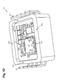
- Figure 1D illustrates a perspective view of a portion of a packaged assembly, according to one implementation of the present application.
- packaged assembly 180 includes case 100 and double-sided substrate 120.
- bottom plate 116 of case 100 in Figure 1B is omitted from Figure 1D for purposes of clarity, but may be included in packaged assembly 180.
- case 100 includes walls 102a, 102b and 102c. Shelf 106a on wall 102a and shelf 106b (not explicitly shown in Figure 1D ) on wall 102b are configured to provide support for double-sided substrate 120. As can be seen in Figure 1D , shelves are not formed on wall 102c or 102d since shelves 106a and 106b on respective opposing walls 102a and 102b are sufficient to provide support for double-sided substrate 120. As illustrated in Figure 1D , semiconductor die 118 and various other circuit elements (e.g., resistors) are formed on front side 122a of double double-sided substrate 120. One or more bond pads 126 are disposed along the perimeters of semiconductor die 118 for wire-bonding.
- semiconductor die 118 and various other circuit elements e.g., resistors
- packaged assembly 180 has a length of approximately 1.0 inch., a width of approximately 1.0 inch., and a height of approximately 0.4 inch. In the present implementation, packaged assembly 180 has an overall weight of approximately 15 grams. In other implementations, packaged assembly 180 may have other dimensions and weight to suit the needs of a particular application.
- double-sided substrate 120 has a length of approximately 0.82 inch., a width of approximately 0.82 inch., and a thickness of approximately of approximately 60 mils (i.e., one sixty thousandth of an inch). In other implementations, double-sided substrate 120 may have other dimensions to suit the needs of a particular application.
- packaged assembly 180 may operate at an input voltage in the range of 3.0 to 13.0 volts and provide an output voltage in the range of 0.6 to 12.0 volts (e.g., 6-9 volts). In other implementations, packaged assembly 180 may operate at an input voltage of less than 3.0 volts or greater than 13.0 volts, and provide an output voltage of less than 0.6 volts or greater than 12 volts.
- a packaged assembly includes a double-sided substrate secured to a lightweight case by an epoxy.
- the case is made of a lightweight, thermally conductive, controlled expansion aluminum silicon matrix.
- the double-sided substrate allows to double the size of the circuitry relative to a conventional layout while keeping the foot print very small.
- the double-sided substrate is made of beryllium oxide or aluminum oxide, which has good matching CTE characteristics with the case made of aluminum silicon, thereby allowing the use of an epoxy to secure the double-sided substrate to the package shelves without a need for additional hardware or hard soldering paste.
- the double-sided substrate interconnects the circuitry on its front side to the circuitry on its back side using silver thick film filled vias for added current carrying capability between both sides.
- the circuitry on the double-sided substrate are electrically coupled to invertible leads made of copper-based metal matrix composite alloys mixed with aluminum, oxide and/or ceramic particles for increased electrical conductivity and mechanical strength.
Landscapes
- Engineering & Computer Science (AREA)
- Microelectronics & Electronic Packaging (AREA)
- Cooling Or The Like Of Semiconductors Or Solid State Devices (AREA)
- Physics & Mathematics (AREA)
- Geometry (AREA)
Abstract
Description
- The present application claims the benefit of and priority to a provisional patent application entitled "Hermetically Packaged Hybrid Assembly with Double-Sided Substrate for High Density Power Applications," Serial Number
62/072,372 filed on October 29, 2014 - Semiconductor power modules control electrical power to circuits and devices, such as motors, actuators, controllers or the like. When high reliability is required for use in extreme or harsh environments, such as in high performance vehicles, aircrafts, space shuttles and satellites, it is important to provide robust packaged assemblies that are small, lightweight, and electrically and thermally efficient. For example, in some space and satellite applications, packaged assemblies with power semiconductor devices require packaging of high thermal conductivity in order to maintain useful operation of the devices. However, most packaging material with good thermal characteristics does not offer matching substrate to package coefficient of thermal expansion (CTE).
- In a conventional packaged assembly, a substrate is attached to a package using hardware and hard soldering paste, which add weight to the packaged assembly. The contact points between the hardware and the substrate consume the limited usable area of the substrate. Moreover, due to a mismatch of coefficient of thermal expansion (CTE) between the substrate and the package, the packaged assembly experiences thermal stress due to changes in temperature, which can cause damage to the power semiconductor devices and circuitry on the substrate.
- Accordingly, there is a need to overcome the drawbacks and deficiencies in the art by providing a small, lightweight, and electrically and thermally efficient packaged assembly for high density power applications.
- The present disclosure is directed to a packaged assembly for high density power applications, substantially as shown in and/or described in connection with at least one of the figures, and as set forth in the claims.
-
-
Figure 1A illustrates a perspective view of a portion of a packaged assembly, according to one implementation of the present application. -
Figure 1B illustrates a perspective view of a portion of a packaged assembly, according to one implementation of the present application. -
Figure 1C illustrates a perspective view of a portion of a packaged assembly, according to one implementation of the present application. -
Figure 1D illustrates a perspective view of a portion of a packaged assembly, according to one implementation of the present application. - The following description contains specific information pertaining to implementations in the present disclosure. The drawings in the present application and their accompanying detailed description are directed to merely exemplary implementations. Unless noted otherwise, like or corresponding elements among the figures may be indicated by like or corresponding reference numerals. Moreover, the drawings and illustrations in the present application are generally not to scale, and are not intended to correspond to actual relative dimensions.
-
Figure 1A illustrates a perspective view of a portion of a packaged assembly, according to one implementation of the present application. As illustrated inFigure 1A , packagedassembly 180 includescase 100, double-sided substrate 120 disposed incase 100, and leads 114 electrically coupled to semiconductor devices and/or circuit elements formed on double-sided substrate 120 throughlead frames 112 for external connection. Among other components, a hermetic lid and an encapsulating molding compound or gap filler are omitted fromFigure 1A for purposes of clarity, but may be included in packagedassembly 180. - In the present implementation,
case 100 includes a hermetic lid (not explicitly shown inFigure 1A ),walls Figure 1A ) on each ofopposing walls sided substrate 120, and a bottom plate (not explicitly shown inFigure 1A ).Case 100 includes a material with low mass, high thermal conductivity and high machinability. In the present implementation,case 100 includes aluminum silicon (AlSi). The high thermal conductivity of AlSi facilitates transferring heat generated by circuit elements and power semiconductor devices on double-sidedsubstrate 120 out of packagedassembly 180. As weight saving is crucial in space and satellite applications,case 100 having AlSi is super lightweight, thereby substantially reducing the overall weight of packagedassembly 180. Moreover, AlSi is highly machinable, which means that the manufacturing process of case 100 (e.g., cutting, removing portions thereof and obtaining a good finish) requires little power and time. With high machinability, it is also easy and quick to make configuration changes to accommodate different footprints of different substrates if needed. In other implementations,case 100 may include other suitable material with low mass, high thermal conductivity and high machinability. Also, as discussed below, the CTE ofcase 100 is closely matched with double-sided substrate 120, such that a change in volume (e.g., expansion or contraction) ofcase 100 in response to a change in temperature does not introduce stress to double-sided substrate 120 or locations in packaged assembly where an epoxy is used to secure double-sided substrate 120 tocase 100. As such, additional hardware and hard soldering paste are not required to secure double-sidedsubstrate 120 in place, thereby further reducing the overall weight of packagedassembly 180. - In the present implementation, double-
sided substrate 120 includes a front side (not explicitly shown inFigure 1A ) and a back side (e.g.,back side 122b). As illustrated inFigure 1A ,back side 122b of double-sided substrate 120 includes various circuit elements formed thereon. As illustrated inFigure 1A ,toroidal inductors ceramic capacitor stacks tantalum capacitors back side 122b of double-sided substrate 120.Toroidal inductors Toroidal inductors sided substrate 120, for example.Tantalum capacitors sided substrate 120, for example.Ceramic capacitor stacks back side 122b of double-sided substrate 120, and configured to filter an input noise of the point of load converter formed on double-sided substrate 120, for example. - As illustrated in
Figure 1A , leads 114 extend throughwalls case 100, and are electrically coupled to power semiconductor devices and/or circuit elements formed on double-sided substrate 120 throughlead frames 112 alongwalls case 100. In the present implementation,leads 114 are invertible leads that can be inverted 180° from their current positions as shown inFigure 1A , such that both the hermetic lid andbottom plate 116 ofcase 100 can be used as a mounting surface for packagedassembly 180. In the present implementation,leads 114 are made of copper-based metal matrix composite alloys mixed with aluminum, oxide and/or ceramic particles.Leads 114 each have a diameter of approximately 30 mils (i.e., one thirty thousandth of an inch), thus allowing for greater current carrying capability and mechanical strength to accommodate power semiconductor devices in packagedassembly 180. In other implementations,leads 114 may be made of other conductive materials, and have a diameter of greater or less than 30 mils. - It should be noted that, in the present implementation, a hermetic lid (not explicitly shown in
Figure 1A ) may be laser welded tocase 100 to hermetically seal double-sided substrate 120 in packagedassembly 180. Also, an encapsulating molding compound or gap filler may partially or entirely fill the space between circuit elements formed onback side 122b of double-sided substrate 120 and the lid, such that hermetically sealed packagedassembly 180 can withstand g-forces of 5000g or more. -
Figure 1B illustrates a perspective view of a portion of a packaged assembly, according to one implementation of the present application. In the present implementation,Figure 1B is a perspective view of packagedassembly 180 along line B-B inFigure 1A . With similar numerals representing similar features inFigure 1A , packagedassembly 180 includescase 100, double-sided substrate 120 disposed onshelf 106a onwall 102a andshelf 106b onwall 102b ofcase 100, respectively. Among other components, a hermetic lid, an encapsulating molding compound or gap filler, andwall 102d inFigure 1A are omitted fromFigure 1B for purposes of clarity, but may be included in packagedassembly 180. - As illustrated in
Figure 1B ,case 100 includeswalls shelves opposing walls case 100, andbottom plate 116. In the present implementation,shelves opposing walls case 100 for providing support for double-sided substrate 120. It should be noted that shelves are not formed onwalls shelves opposing walls substrate 120. As a consequence, additional hardware is not required to secure double-sidedsubstrate 120 tocase 100, thereby substantially reducing the overall weight of packagedassembly 180. - In the present implementation,
shelves case 100 through a machine process. For example,shelves case 100 by grindingcase 100 from a top surface todepth 103 to form upper portions ofwalls case 100, then removing another portion ofcase 100 belowdepth 103 leaving a narrower width betweenopposing walls walls Figure 1B ,width 107a ofshelf 106a is greater thanwidth 109a of the upper portion ofwall 102a. Similarly,width 107b ofshelf 106b is greater thanwidth 109b of the upper portion ofwall 102b. Sinceshelves sided substrate 120 at its edges, the contact area between double-sided substrate 120 andcase 100 is minimized, thereby allowing more circuit elements and semiconductor devices to be built on both sides of double-sided substrate 120. As such, a high density substrate can be formed. Height 105a ofshelf 106a is equal toheight 105b ofshelf 106b such that double-sided substrate 120 can be situated above and substantially parallel withbottom plate 116.Heights 105a and 105b may be of any appropriate value to provide sufficient clearance for semiconductor dies and circuit elements formed onfront side 122a of double-sided substrate 120. - In the present implementation, double-
sided substrate 120 is a thick film substrate made of beryllium oxide (BeO) or aluminum oxide (Al2O3). In other implementations, double-sided substrate 120 may include other suitable dielectric material. In the present implementation, double-sided substrate 120 is a single substrate, such as a PC board, which allows one or more semiconductor dies and circuit elements to be attached to both sides of the substrate. By using both sides of a single substrate, for example, of uniform composition, double-sided substrate 120 does not require wafer bonding steps to bond two substrates together, for example, using copper, thereby reducing manufacturing complexity and cost. In one implementation, packagedassembly 180 can be a hybrid assembly having bare semiconductor dies and packaged integrated circuits directly attached thereto. - As illustrated in
Figure 1B , double-sided substrate 120 includestoroidal inductors ceramic capacitor stacks tantalum capacitors back side 122b of double-sided substrate 120. As illustrated inFigure 1B , double-sided substrate 120 also includes various circuit elements formed onfront side 122a of double-sided substrate 120. In contrast to conventional assemblies where only one side of a substrate is used for receive circuit elements and semiconductor devices, implementations of the present application can double the usable area to which semiconductor dies and circuit elements can be attached, through the utilization of bothfront side 122a and backside 122b of double-sided substrate 120. As illustrated inFigure 1B , leads 114 extend throughwall 102c ofcase 100, and are electrically coupled to semiconductor devices and/or circuit elements formed on double-sided substrate 120 throughlead frames 112 alongwall 102c ofcase 100. In one implementation, leads 114 may be soldered to leadframes 112. - It should be noted that an epoxy may be applied and cured to
perimeters Figure 1B ) alongwalls sided substrate 120 tocase 100. In the present implementation, the epoxy may include any suitable material, such as commercially available ME7155 by AI Tech. In the present implementation,case 100 includes AlSi. Double-sided substrate 120 may include a material (e.g., Al2O3 or BeO) having a CTE closely matched with that ofcase 100. As a result, a change in volume (e.g., expansion or contraction) ofcase 100 in response to a change in temperature does not introduce stress to double-sided substrate 120 orperimeters sided substrate 120 tocase 100. As such, additional hardware and hard soldering paste are not required to secure double-sided substrate 120 in place, thereby substantially reducing the overall weight of packagedassembly 180. -
Figure 1C illustrates a perspective view of a portion of a packaged assembly, according to one implementation of the present application. In the present implementation,Figure 1C is a perspective view of packagedassembly 180 along line C-C inFigure 1A . With similar numerals representing similar features inFigure 1A , packagedassembly 180 includescase 100 and double-sided substrate 120 having throughsubstrate vias front side 122a to backside 122b of double-sided substrate 120. Among other components, a hermetic lid, an encapsulating molding compound or gap filler, andwall 102a inFigure 1A are omitted fromFigure 1C for purposes of clarity, but may be included in packagedassembly 180. - In the present implementation,
walls 102b having shelf 106b, andbottom plate 116 ofcase 100 are shown inFigure 1C . It is noted that, in contrast towalls shelves Figure 1B ,walls Figure 1C ,walls uniform thicknesses shelves walls sided substrate 120, additional shelves are not required onwalls case 100, thus reducing the overall weight of packagedassembly 180. In the present implementation,thickness 109c ofwall 102c is substantially equal tothickness 109d ofwall 102d. In another implementation,thickness 109c ofwall 102c andthickness 109d ofwall 102d may be different. - In the present implementation, double-
sided substrate 120 may include a power conversion circuit, such as a point of load converter formed thereon. For example, double-sided substrate 120 may include a pulse width modulator configured to generate control signals, which are pulse width modulated control signals. In one implementation, the pulse width modulator can perform two and/or three phase pulse width modulation to drive an inverter circuit (e.g., having a two or three phase bridge connected circuit) integrated on double-sided substrate 120. As illustrated inFigure 1C ,toroidal inductors ceramic capacitor stack 108a,tantalum capacitor 110b and various other circuit elements are shown onback side 122b of double-sided substrate 120. Also, semiconductor die 118 and various other circuit elements are formed onfront side 122a of double-sided substrate 120. - In the present implementation, semiconductor die 118 includes a pulse width modulator (not explicitly shown in
Figure 1C ) and various other circuits monolithically integrated thereon. In the present implementation, semiconductor die 118 includes silicon. In other implementations, semiconductor die 118 may include other suitable semiconductor material such as silicon-on-sapphire (SOS), silicon carbide (SiC), or the like. In the present implementation, semiconductor die 118 includes one or more power semiconductor devices (not explicitly shown inFigure 1C ). For example, semiconductor die 118 may include lateral and/or vertical conduction power semiconductor devices, such as field-effect transistors (FETs) or insulated-gate bipolar transistors (IGBTs), or the like. - As illustrated in
Figure 1C , semiconductor die 118 is directly attached tofront side 122a of double-sided substrate 120. In one implementation, a power electrode of at least one power semiconductor device is attached tofront side 122a of double-sided substrate 120, and is mechanically and electrically coupled to one or more circuit elements onback side 122b of double-sided substrate 120 through one or more TSVs, such asTSVs Figure 1C . In one implementation, one or more TSVs can be utilized to provide routing and/or electrical connection between various circuit elements onback side 122b and a back side metal of semiconductor die 118 onfront side 122a in any desired manner. In another implementation, one or more TSVs can serve to ground semiconductor die 118. - As illustrated in
Figure 1C , TSVs 124a and 124b may be metalized holes in double-sided substrate 120. In the present implementation,TSVs front side 122a and backside 122b of double-sided substrate 120. It should be noted that although only TSVs 124a and 124b are shown inFigure 1C , double-sided substrate 120 may include additional TSVs extending fromfront side 122a to backside 122b of double-sided substrate 120, and electrically coupling circuit elements and semiconductor dies onfront side 122a to circuit elements and semiconductor dies onback side 122b of double-sided substrate 120. - It should be understood that
walls bottom plate 116 and a hermetic lid (not explicitly shown inFigure 1C ) form a hermetically sealed case enclosing double-sided substrate 120 and all semiconductor dies and circuit elements formed thereon.Leads 114 extend throughwalls sided substrate 120 by lead frames 112. - As discussed above, semiconductor die 118 is directly attached to
front side 122a of double-sided substrate 120. As power semiconductor devices on semiconductor die 118 require packaging that has high thermal conductivity in order to maintain useful operation of the devices,case 100 having AlSi not only has good thermal characteristics, but also matching CTE characteristics with double-sided substrate 120 having BeO or Al2O3, for example. In one implementation, double-sided substrate 120 may also have good thermal characteristics to improve the thermal management on semiconductor dies and circuit elements formed thereon. Thus, in contrast to conventional assemblies with poorly matched substrate to package CTEs which require hard soldering paste, implementations of the present application only requires an epoxy applied alongperimeters sided substrate 120 to secure double-sided substrate 120 tocase 100. In addition, since additional hardware and hard soldering paste are not required to secure double-sided substrate 120 tocase 100, packagedassembly 180 can have an very low mass (e.g., 15 grams or less). -
Figure 1D illustrates a perspective view of a portion of a packaged assembly, according to one implementation of the present application. With similar numerals representing similar features inFigure 1A , packagedassembly 180 includescase 100 and double-sided substrate 120. Among other components,bottom plate 116 ofcase 100 inFigure 1B is omitted fromFigure 1D for purposes of clarity, but may be included in packagedassembly 180. - As illustrated in
Figure 1D ,case 100 includeswalls Shelf 106a onwall 102a andshelf 106b (not explicitly shown inFigure 1D ) onwall 102b are configured to provide support for double-sided substrate 120. As can be seen inFigure 1D , shelves are not formed onwall shelves walls sided substrate 120. As illustrated inFigure 1D , semiconductor die 118 and various other circuit elements (e.g., resistors) are formed onfront side 122a of double double-sided substrate 120. One ormore bond pads 126 are disposed along the perimeters of semiconductor die 118 for wire-bonding. - In the present implementation, packaged
assembly 180 has a length of approximately 1.0 inch., a width of approximately 1.0 inch., and a height of approximately 0.4 inch. In the present implementation, packagedassembly 180 has an overall weight of approximately 15 grams. In other implementations, packagedassembly 180 may have other dimensions and weight to suit the needs of a particular application. In the present implementation, double-sided substrate 120 has a length of approximately 0.82 inch., a width of approximately 0.82 inch., and a thickness of approximately of approximately 60 mils (i.e., one sixty thousandth of an inch). In other implementations, double-sided substrate 120 may have other dimensions to suit the needs of a particular application. In the present implementation, packagedassembly 180 may operate at an input voltage in the range of 3.0 to 13.0 volts and provide an output voltage in the range of 0.6 to 12.0 volts (e.g., 6-9 volts). In other implementations, packagedassembly 180 may operate at an input voltage of less than 3.0 volts or greater than 13.0 volts, and provide an output voltage of less than 0.6 volts or greater than 12 volts. - According to one implementation of the present application, a packaged assembly includes a double-sided substrate secured to a lightweight case by an epoxy. In one implementation, the case is made of a lightweight, thermally conductive, controlled expansion aluminum silicon matrix. In one implementation, the double-sided substrate allows to double the size of the circuitry relative to a conventional layout while keeping the foot print very small. In one implementation, the double-sided substrate is made of beryllium oxide or aluminum oxide, which has good matching CTE characteristics with the case made of aluminum silicon, thereby allowing the use of an epoxy to secure the double-sided substrate to the package shelves without a need for additional hardware or hard soldering paste. In one implementation, the double-sided substrate interconnects the circuitry on its front side to the circuitry on its back side using silver thick film filled vias for added current carrying capability between both sides. In one implementation, the circuitry on the double-sided substrate are electrically coupled to invertible leads made of copper-based metal matrix composite alloys mixed with aluminum, oxide and/or ceramic particles for increased electrical conductivity and mechanical strength. Thus, implementations of the present application combine high density circuitry with a lightweight case that has excellent thermal conductivity, which allow for a high power performance, low mass, and small footprint point of load packaged assembly, for example.
- From the above description it is manifest that various techniques can be used for implementing the concepts described in the present application without departing from the scope of those concepts. Moreover, while the concepts have been described with specific reference to certain implementations, a person of ordinary skill in the art would recognize that changes can be made in form and detail without departing from the scope of those concepts. As such, the described implementations are to be considered in all respects as illustrative and not restrictive. It should also be understood that the present application is not limited to the particular implementations described herein, but many rearrangements, modifications, and substitutions are possible without departing from the scope of the present disclosure.
Claims (15)
- A packaged assembly for high density power applications, the packaged assembly comprising:a case having shelves on opposing walls;a double-sided substrate disposed on said shelves of said case, said double-sided substrate having a semiconductor die on a first side of said double-sided substrate and circuit elements on a second side of said double-sided substrate.
- The packaged assembly of claim 1 wherein said case comprises aluminum silicon (AlSi).
- The packaged assembly of claim 1 wherein said double-sided substrate comprises beryllium oxide (BeO) or aluminum oxide (Al2O3).
- The packaged assembly of claim 1 wherein said semiconductor die on said first side of said double-sided substrate is coupled to at least one of said circuit elements on said second side of said double-sided substrate by a through substrate via.
- The packaged assembly of claim 1 wherein said double-sided substrate is a thick film substrate.
- The packaged assembly of claim 1 wherein said semiconductor die includes a pulse width modulator.
- The packaged assembly of claim 1 wherein said semiconductor die includes at least one vertical conduction semiconductor device.
- The packaged assembly of claim 1 further comprising invertible leads coupled to said double-sided substrate by lead frames.
- The packaged assembly of claim 1 wherein a point of load converter circuit is formed on said double-sided substrate.
- The packaged assembly of claim 1 wherein said double-sided substrate is secured to said shelves of said case by an epoxy.
- A packaged assembly comprising:a case having aluminum silicon (AlSi);a double-sided substrate disposed on shelves of said case, said double-sided substrate having a semiconductor die on a first side of said double-sided substrate coupled to at least one circuit element on a second side of said double-sided substrate.
- The packaged assembly of claim 11 wherein said shelves are on opposing walls of said case.
- The packaged assembly of claim 11 wherein said double-sided substrate comprises beryllium oxide (BeO) or aluminum oxide (Al2O3).
- The packaged assembly of claim 11 wherein said semiconductor die on said first side of said double-sided substrate is coupled to at least one of said circuit elements on said second side of said double-sided substrate by a through substrate via.
- The packaged assembly of claim 11 wherein said double-sided substrate is a thick film substrate.
Applications Claiming Priority (2)
| Application Number | Priority Date | Filing Date | Title |
|---|---|---|---|
| US201462072372P | 2014-10-29 | 2014-10-29 | |
| US14/877,059 US10319674B2 (en) | 2014-10-29 | 2015-10-07 | Packaged assembly for high density power applications |
Publications (2)
| Publication Number | Publication Date |
|---|---|
| EP3016138A1 true EP3016138A1 (en) | 2016-05-04 |
| EP3016138B1 EP3016138B1 (en) | 2021-05-12 |
Family
ID=54292736
Family Applications (1)
| Application Number | Title | Priority Date | Filing Date |
|---|---|---|---|
| EP15189330.2A Active EP3016138B1 (en) | 2014-10-29 | 2015-10-12 | Packaged assembly for high density power applications |
Country Status (2)
| Country | Link |
|---|---|
| US (1) | US10319674B2 (en) |
| EP (1) | EP3016138B1 (en) |
Families Citing this family (1)
| Publication number | Priority date | Publication date | Assignee | Title |
|---|---|---|---|---|
| US11488764B2 (en) | 2018-10-09 | 2022-11-01 | Delta Electronics, Inc. | Voltage regulator module |
Citations (3)
| Publication number | Priority date | Publication date | Assignee | Title |
|---|---|---|---|---|
| US5311407A (en) * | 1992-04-30 | 1994-05-10 | Siemens Components, Inc. | Printed circuit based for mounted semiconductors and other electronic components |
| JP2007049099A (en) * | 2005-08-12 | 2007-02-22 | Murata Mfg Co Ltd | Ceramic electronic component and manufacturing method thereof |
| US20080053700A1 (en) * | 2006-09-06 | 2008-03-06 | O'connor Kurt F | Sealed electronic component |
Family Cites Families (25)
| Publication number | Priority date | Publication date | Assignee | Title |
|---|---|---|---|---|
| JP2725637B2 (en) * | 1995-05-31 | 1998-03-11 | 日本電気株式会社 | Electronic circuit device and method of manufacturing the same |
| DE59713027D1 (en) * | 1996-09-30 | 2010-03-25 | Infineon Technologies Ag | MICROELECTRONIC COMPONENT IN SANDWICH CONSTRUCTION |
| US6424034B1 (en) * | 1998-08-31 | 2002-07-23 | Micron Technology, Inc. | High performance packaging for microprocessors and DRAM chips which minimizes timing skews |
| US6890798B2 (en) * | 1999-06-08 | 2005-05-10 | Intel Corporation | Stacked chip packaging |
| US6958535B2 (en) * | 2000-09-22 | 2005-10-25 | Matsushita Electric Industrial Co., Ltd. | Thermal conductive substrate and semiconductor module using the same |
| JP3846437B2 (en) * | 2003-03-17 | 2006-11-15 | 株式会社日立製作所 | Automotive control unit |
| US7132746B2 (en) * | 2003-08-18 | 2006-11-07 | Delphi Technologies, Inc. | Electronic assembly with solder-bonded heat sink |
| JP4347009B2 (en) * | 2003-09-26 | 2009-10-21 | キヤノン株式会社 | Near-field light generation method, near-field exposure mask, near-field exposure method, near-field exposure apparatus, near-field light head |
| DE10348620A1 (en) * | 2003-10-15 | 2005-06-02 | Infineon Technologies Ag | Semiconductor module with housing contacts |
| JP4258367B2 (en) * | 2003-12-18 | 2009-04-30 | 株式会社日立製作所 | Optical component mounting package and manufacturing method thereof |
| KR100640335B1 (en) * | 2004-10-28 | 2006-10-30 | 삼성전자주식회사 | Land grid array module |
| TWI271142B (en) * | 2005-05-09 | 2007-01-11 | Benq Corp | Electronic device |
| JP4434181B2 (en) * | 2006-07-21 | 2010-03-17 | 株式会社日立製作所 | Power converter |
| US20080023824A1 (en) * | 2006-07-28 | 2008-01-31 | Texas Instruments | Double-sided die |
| TW200915970A (en) * | 2007-09-27 | 2009-04-01 | Sanyo Electric Co | Circuit device, circuit module and outdoor equipment |
| KR101448849B1 (en) * | 2007-11-16 | 2014-10-14 | 페어차일드코리아반도체 주식회사 | Power module and manufacturing method thereof |
| US8207607B2 (en) * | 2007-12-14 | 2012-06-26 | Denso Corporation | Semiconductor device with resin mold |
| CN101978490B (en) * | 2008-03-31 | 2012-10-17 | 株式会社村田制作所 | Electronic component assembly and method for manufacturing the electronic component assembly |
| US8358017B2 (en) * | 2008-05-15 | 2013-01-22 | Gem Services, Inc. | Semiconductor package featuring flip-chip die sandwiched between metal layers |
| DE102009045181B4 (en) * | 2009-09-30 | 2020-07-09 | Infineon Technologies Ag | Power semiconductor module |
| US8232615B2 (en) * | 2010-02-23 | 2012-07-31 | Avago Technologies Wireless Ip (Singapore) Pte. Ltd. | Packaged device with acoustic transducer and amplifier |
| JP4948613B2 (en) * | 2010-02-25 | 2012-06-06 | 三菱電機株式会社 | Resin-sealed electronic control device and manufacturing method thereof |
| JP5474877B2 (en) | 2011-06-17 | 2014-04-16 | 日立オートモティブシステムズ株式会社 | Electronic control unit |
| US9601417B2 (en) * | 2011-07-20 | 2017-03-21 | Unigen Corporation | “L” shaped lead integrated circuit package |
| KR101443972B1 (en) * | 2012-10-31 | 2014-09-23 | 삼성전기주식회사 | All-in-one power semiconductor module |
-
2015
- 2015-10-07 US US14/877,059 patent/US10319674B2/en active Active
- 2015-10-12 EP EP15189330.2A patent/EP3016138B1/en active Active
Patent Citations (3)
| Publication number | Priority date | Publication date | Assignee | Title |
|---|---|---|---|---|
| US5311407A (en) * | 1992-04-30 | 1994-05-10 | Siemens Components, Inc. | Printed circuit based for mounted semiconductors and other electronic components |
| JP2007049099A (en) * | 2005-08-12 | 2007-02-22 | Murata Mfg Co Ltd | Ceramic electronic component and manufacturing method thereof |
| US20080053700A1 (en) * | 2006-09-06 | 2008-03-06 | O'connor Kurt F | Sealed electronic component |
Non-Patent Citations (1)
| Title |
|---|
| QI-JIN JIA ET AL: "Microstructure and properties of electronic packaging box with high silicon aluminum-base alloy by semi-solid thixoforming", TRANSACTIONS OF NONFERROUS METALS SOCIETY OF CHINA, vol. 23, no. 1, 1 January 2013 (2013-01-01), CN, pages 80 - 85, XP055251842, ISSN: 1003-6326, DOI: 10.1016/S1003-6326(13)62432-2 * |
Also Published As
| Publication number | Publication date |
|---|---|
| EP3016138B1 (en) | 2021-05-12 |
| US10319674B2 (en) | 2019-06-11 |
| US20160126177A1 (en) | 2016-05-05 |
Similar Documents
| Publication | Publication Date | Title |
|---|---|---|
| CN100524737C (en) | Power module, Phase leg, and three-phase inverter | |
| JP4438489B2 (en) | Semiconductor device | |
| US9385107B2 (en) | Multichip device including a substrate | |
| US9899282B2 (en) | Robust high performance semiconductor package | |
| CN108735689B (en) | Chip module with space-limited thermally conductive mount | |
| US11329025B2 (en) | Multi-chip package with reinforced isolation | |
| US10770382B2 (en) | Low inductance stackable solid-state switching module and method of manufacturing thereof | |
| KR20140113451A (en) | Power overlay structure and method of making same | |
| KR101321277B1 (en) | Power module package and method for manufacturing the same | |
| JP2018120902A (en) | Power electronics package and method of manufacturing the same | |
| KR20140113473A (en) | Power overlay structure and method of making same | |
| US11908760B2 (en) | Package with encapsulated electronic component between laminate and thermally conductive carrier | |
| CN104425470A (en) | Semiconductor module and a method for fabrication thereof by extended embedding technologies | |
| US10685909B2 (en) | Power package having multiple mold compounds | |
| US20130286617A1 (en) | Circuit device | |
| CN110880488B (en) | Semiconductor device and power conversion device | |
| JP2016046497A (en) | Power semiconductor device and method of manufacturing power semiconductor device | |
| JP6935976B2 (en) | Power modules and how to manufacture power modules | |
| US20180040562A1 (en) | Elektronisches modul und verfahren zu seiner herstellung | |
| EP3016138B1 (en) | Packaged assembly for high density power applications | |
| US9698076B1 (en) | Metal slugs for double-sided cooling of power module | |
| US12414236B2 (en) | Electronic device with castellated board | |
| WO2013157172A1 (en) | Semiconductor package and method for producing same, semiconductor module, and semiconductor device | |
| KR101216777B1 (en) | Power module package and method for manufacturing the same | |
| KR20260014303A (en) | Ceramic circuit board having unidirectional porous metal spacer and power module having the same |
Legal Events
| Date | Code | Title | Description |
|---|---|---|---|
| PUAI | Public reference made under article 153(3) epc to a published international application that has entered the european phase |
Free format text: ORIGINAL CODE: 0009012 |
|
| AK | Designated contracting states |
Kind code of ref document: A1 Designated state(s): AL AT BE BG CH CY CZ DE DK EE ES FI FR GB GR HR HU IE IS IT LI LT LU LV MC MK MT NL NO PL PT RO RS SE SI SK SM TR |
|
| AX | Request for extension of the european patent |
Extension state: BA ME |
|
| 17P | Request for examination filed |
Effective date: 20161006 |
|
| RBV | Designated contracting states (corrected) |
Designated state(s): AL AT BE BG CH CY CZ DE DK EE ES FI FR GB GR HR HU IE IS IT LI LT LU LV MC MK MT NL NO PL PT RO RS SE SI SK SM TR |
|
| STAA | Information on the status of an ep patent application or granted ep patent |
Free format text: STATUS: EXAMINATION IS IN PROGRESS |
|
| 17Q | First examination report despatched |
Effective date: 20161216 |
|
| RAP1 | Party data changed (applicant data changed or rights of an application transferred) |
Owner name: INFINEON TECHNOLOGIES AMERICAS CORP. |
|
| GRAP | Despatch of communication of intention to grant a patent |
Free format text: ORIGINAL CODE: EPIDOSNIGR1 |
|
| STAA | Information on the status of an ep patent application or granted ep patent |
Free format text: STATUS: GRANT OF PATENT IS INTENDED |
|
| INTG | Intention to grant announced |
Effective date: 20201204 |
|
| GRAS | Grant fee paid |
Free format text: ORIGINAL CODE: EPIDOSNIGR3 |
|
| GRAA | (expected) grant |
Free format text: ORIGINAL CODE: 0009210 |
|
| STAA | Information on the status of an ep patent application or granted ep patent |
Free format text: STATUS: THE PATENT HAS BEEN GRANTED |
|
| AK | Designated contracting states |
Kind code of ref document: B1 Designated state(s): AL AT BE BG CH CY CZ DE DK EE ES FI FR GB GR HR HU IE IS IT LI LT LU LV MC MK MT NL NO PL PT RO RS SE SI SK SM TR |
|
| REG | Reference to a national code |
Ref country code: GB Ref legal event code: FG4D |
|
| REG | Reference to a national code |
Ref country code: CH Ref legal event code: EP |
|
| REG | Reference to a national code |
Ref country code: DE Ref legal event code: R096 Ref document number: 602015069190 Country of ref document: DE |
|
| REG | Reference to a national code |
Ref country code: IE Ref legal event code: FG4D |
|
| REG | Reference to a national code |
Ref country code: AT Ref legal event code: REF Ref document number: 1392742 Country of ref document: AT Kind code of ref document: T Effective date: 20210615 |
|
| REG | Reference to a national code |
Ref country code: LT Ref legal event code: MG9D |
|
| REG | Reference to a national code |
Ref country code: AT Ref legal event code: MK05 Ref document number: 1392742 Country of ref document: AT Kind code of ref document: T Effective date: 20210512 |
|
| REG | Reference to a national code |
Ref country code: NL Ref legal event code: MP Effective date: 20210512 |
|
| PG25 | Lapsed in a contracting state [announced via postgrant information from national office to epo] |
Ref country code: LT Free format text: LAPSE BECAUSE OF FAILURE TO SUBMIT A TRANSLATION OF THE DESCRIPTION OR TO PAY THE FEE WITHIN THE PRESCRIBED TIME-LIMIT Effective date: 20210512 Ref country code: FI Free format text: LAPSE BECAUSE OF FAILURE TO SUBMIT A TRANSLATION OF THE DESCRIPTION OR TO PAY THE FEE WITHIN THE PRESCRIBED TIME-LIMIT Effective date: 20210512 Ref country code: AT Free format text: LAPSE BECAUSE OF FAILURE TO SUBMIT A TRANSLATION OF THE DESCRIPTION OR TO PAY THE FEE WITHIN THE PRESCRIBED TIME-LIMIT Effective date: 20210512 Ref country code: BG Free format text: LAPSE BECAUSE OF FAILURE TO SUBMIT A TRANSLATION OF THE DESCRIPTION OR TO PAY THE FEE WITHIN THE PRESCRIBED TIME-LIMIT Effective date: 20210812 Ref country code: HR Free format text: LAPSE BECAUSE OF FAILURE TO SUBMIT A TRANSLATION OF THE DESCRIPTION OR TO PAY THE FEE WITHIN THE PRESCRIBED TIME-LIMIT Effective date: 20210512 |
|
| PG25 | Lapsed in a contracting state [announced via postgrant information from national office to epo] |
Ref country code: IS Free format text: LAPSE BECAUSE OF FAILURE TO SUBMIT A TRANSLATION OF THE DESCRIPTION OR TO PAY THE FEE WITHIN THE PRESCRIBED TIME-LIMIT Effective date: 20210912 Ref country code: GR Free format text: LAPSE BECAUSE OF FAILURE TO SUBMIT A TRANSLATION OF THE DESCRIPTION OR TO PAY THE FEE WITHIN THE PRESCRIBED TIME-LIMIT Effective date: 20210813 Ref country code: LV Free format text: LAPSE BECAUSE OF FAILURE TO SUBMIT A TRANSLATION OF THE DESCRIPTION OR TO PAY THE FEE WITHIN THE PRESCRIBED TIME-LIMIT Effective date: 20210512 Ref country code: NO Free format text: LAPSE BECAUSE OF FAILURE TO SUBMIT A TRANSLATION OF THE DESCRIPTION OR TO PAY THE FEE WITHIN THE PRESCRIBED TIME-LIMIT Effective date: 20210812 Ref country code: PT Free format text: LAPSE BECAUSE OF FAILURE TO SUBMIT A TRANSLATION OF THE DESCRIPTION OR TO PAY THE FEE WITHIN THE PRESCRIBED TIME-LIMIT Effective date: 20210913 Ref country code: PL Free format text: LAPSE BECAUSE OF FAILURE TO SUBMIT A TRANSLATION OF THE DESCRIPTION OR TO PAY THE FEE WITHIN THE PRESCRIBED TIME-LIMIT Effective date: 20210512 Ref country code: ES Free format text: LAPSE BECAUSE OF FAILURE TO SUBMIT A TRANSLATION OF THE DESCRIPTION OR TO PAY THE FEE WITHIN THE PRESCRIBED TIME-LIMIT Effective date: 20210512 Ref country code: RS Free format text: LAPSE BECAUSE OF FAILURE TO SUBMIT A TRANSLATION OF THE DESCRIPTION OR TO PAY THE FEE WITHIN THE PRESCRIBED TIME-LIMIT Effective date: 20210512 Ref country code: SE Free format text: LAPSE BECAUSE OF FAILURE TO SUBMIT A TRANSLATION OF THE DESCRIPTION OR TO PAY THE FEE WITHIN THE PRESCRIBED TIME-LIMIT Effective date: 20210512 |
|
| PG25 | Lapsed in a contracting state [announced via postgrant information from national office to epo] |
Ref country code: NL Free format text: LAPSE BECAUSE OF FAILURE TO SUBMIT A TRANSLATION OF THE DESCRIPTION OR TO PAY THE FEE WITHIN THE PRESCRIBED TIME-LIMIT Effective date: 20210512 |
|
| PG25 | Lapsed in a contracting state [announced via postgrant information from national office to epo] |
Ref country code: RO Free format text: LAPSE BECAUSE OF FAILURE TO SUBMIT A TRANSLATION OF THE DESCRIPTION OR TO PAY THE FEE WITHIN THE PRESCRIBED TIME-LIMIT Effective date: 20210512 Ref country code: SM Free format text: LAPSE BECAUSE OF FAILURE TO SUBMIT A TRANSLATION OF THE DESCRIPTION OR TO PAY THE FEE WITHIN THE PRESCRIBED TIME-LIMIT Effective date: 20210512 Ref country code: SK Free format text: LAPSE BECAUSE OF FAILURE TO SUBMIT A TRANSLATION OF THE DESCRIPTION OR TO PAY THE FEE WITHIN THE PRESCRIBED TIME-LIMIT Effective date: 20210512 Ref country code: DK Free format text: LAPSE BECAUSE OF FAILURE TO SUBMIT A TRANSLATION OF THE DESCRIPTION OR TO PAY THE FEE WITHIN THE PRESCRIBED TIME-LIMIT Effective date: 20210512 Ref country code: EE Free format text: LAPSE BECAUSE OF FAILURE TO SUBMIT A TRANSLATION OF THE DESCRIPTION OR TO PAY THE FEE WITHIN THE PRESCRIBED TIME-LIMIT Effective date: 20210512 Ref country code: CZ Free format text: LAPSE BECAUSE OF FAILURE TO SUBMIT A TRANSLATION OF THE DESCRIPTION OR TO PAY THE FEE WITHIN THE PRESCRIBED TIME-LIMIT Effective date: 20210512 |
|
| REG | Reference to a national code |
Ref country code: DE Ref legal event code: R097 Ref document number: 602015069190 Country of ref document: DE |
|
| PLBE | No opposition filed within time limit |
Free format text: ORIGINAL CODE: 0009261 |
|
| STAA | Information on the status of an ep patent application or granted ep patent |
Free format text: STATUS: NO OPPOSITION FILED WITHIN TIME LIMIT |
|
| 26N | No opposition filed |
Effective date: 20220215 |
|
| REG | Reference to a national code |
Ref country code: CH Ref legal event code: PL |
|
| PG25 | Lapsed in a contracting state [announced via postgrant information from national office to epo] |
Ref country code: IS Free format text: LAPSE BECAUSE OF FAILURE TO SUBMIT A TRANSLATION OF THE DESCRIPTION OR TO PAY THE FEE WITHIN THE PRESCRIBED TIME-LIMIT Effective date: 20210912 Ref country code: AL Free format text: LAPSE BECAUSE OF FAILURE TO SUBMIT A TRANSLATION OF THE DESCRIPTION OR TO PAY THE FEE WITHIN THE PRESCRIBED TIME-LIMIT Effective date: 20210512 |
|
| REG | Reference to a national code |
Ref country code: BE Ref legal event code: MM Effective date: 20211031 |
|
| PG25 | Lapsed in a contracting state [announced via postgrant information from national office to epo] |
Ref country code: MC Free format text: LAPSE BECAUSE OF FAILURE TO SUBMIT A TRANSLATION OF THE DESCRIPTION OR TO PAY THE FEE WITHIN THE PRESCRIBED TIME-LIMIT Effective date: 20210512 |
|
| PG25 | Lapsed in a contracting state [announced via postgrant information from national office to epo] |
Ref country code: LU Free format text: LAPSE BECAUSE OF NON-PAYMENT OF DUE FEES Effective date: 20211012 Ref country code: IT Free format text: LAPSE BECAUSE OF FAILURE TO SUBMIT A TRANSLATION OF THE DESCRIPTION OR TO PAY THE FEE WITHIN THE PRESCRIBED TIME-LIMIT Effective date: 20210512 Ref country code: BE Free format text: LAPSE BECAUSE OF NON-PAYMENT OF DUE FEES Effective date: 20211031 |
|
| PG25 | Lapsed in a contracting state [announced via postgrant information from national office to epo] |
Ref country code: LI Free format text: LAPSE BECAUSE OF NON-PAYMENT OF DUE FEES Effective date: 20211031 Ref country code: CH Free format text: LAPSE BECAUSE OF NON-PAYMENT OF DUE FEES Effective date: 20211031 |
|
| PG25 | Lapsed in a contracting state [announced via postgrant information from national office to epo] |
Ref country code: IE Free format text: LAPSE BECAUSE OF NON-PAYMENT OF DUE FEES Effective date: 20211012 |
|
| PG25 | Lapsed in a contracting state [announced via postgrant information from national office to epo] |
Ref country code: HU Free format text: LAPSE BECAUSE OF FAILURE TO SUBMIT A TRANSLATION OF THE DESCRIPTION OR TO PAY THE FEE WITHIN THE PRESCRIBED TIME-LIMIT; INVALID AB INITIO Effective date: 20151012 |
|
| PG25 | Lapsed in a contracting state [announced via postgrant information from national office to epo] |
Ref country code: CY Free format text: LAPSE BECAUSE OF FAILURE TO SUBMIT A TRANSLATION OF THE DESCRIPTION OR TO PAY THE FEE WITHIN THE PRESCRIBED TIME-LIMIT Effective date: 20210512 |
|
| P01 | Opt-out of the competence of the unified patent court (upc) registered |
Effective date: 20230528 |
|
| PG25 | Lapsed in a contracting state [announced via postgrant information from national office to epo] |
Ref country code: MK Free format text: LAPSE BECAUSE OF FAILURE TO SUBMIT A TRANSLATION OF THE DESCRIPTION OR TO PAY THE FEE WITHIN THE PRESCRIBED TIME-LIMIT Effective date: 20210512 |
|
| PG25 | Lapsed in a contracting state [announced via postgrant information from national office to epo] |
Ref country code: TR Free format text: LAPSE BECAUSE OF FAILURE TO SUBMIT A TRANSLATION OF THE DESCRIPTION OR TO PAY THE FEE WITHIN THE PRESCRIBED TIME-LIMIT Effective date: 20210512 |
|
| PG25 | Lapsed in a contracting state [announced via postgrant information from national office to epo] |
Ref country code: MT Free format text: LAPSE BECAUSE OF FAILURE TO SUBMIT A TRANSLATION OF THE DESCRIPTION OR TO PAY THE FEE WITHIN THE PRESCRIBED TIME-LIMIT Effective date: 20210512 |
|
| REG | Reference to a national code |
Ref country code: DE Ref legal event code: R079 Ref document number: 602015069190 Country of ref document: DE Free format text: PREVIOUS MAIN CLASS: H01L0023040000 Ipc: H10W0076120000 |
|
| PGFP | Annual fee paid to national office [announced via postgrant information from national office to epo] |
Ref country code: DE Payment date: 20251217 Year of fee payment: 11 |
|
| PGFP | Annual fee paid to national office [announced via postgrant information from national office to epo] |
Ref country code: GB Payment date: 20251022 Year of fee payment: 11 |
|
| PGFP | Annual fee paid to national office [announced via postgrant information from national office to epo] |
Ref country code: FR Payment date: 20251030 Year of fee payment: 11 |