EP3015909A1 - Anzeigevorrichtung - Google Patents
Anzeigevorrichtung Download PDFInfo
- Publication number
- EP3015909A1 EP3015909A1 EP15191309.2A EP15191309A EP3015909A1 EP 3015909 A1 EP3015909 A1 EP 3015909A1 EP 15191309 A EP15191309 A EP 15191309A EP 3015909 A1 EP3015909 A1 EP 3015909A1
- Authority
- EP
- European Patent Office
- Prior art keywords
- display apparatus
- display
- plastic core
- bottom chassis
- display panel
- Prior art date
- Legal status (The legal status is an assumption and is not a legal conclusion. Google has not performed a legal analysis and makes no representation as to the accuracy of the status listed.)
- Granted
Links
- 239000000463 material Substances 0.000 claims abstract description 103
- 229920003023 plastic Polymers 0.000 claims abstract description 83
- 239000004033 plastic Substances 0.000 claims abstract description 83
- 239000002131 composite material Substances 0.000 claims description 16
- 239000004698 Polyethylene Substances 0.000 claims description 12
- 239000004743 Polypropylene Substances 0.000 claims description 12
- 238000000034 method Methods 0.000 claims description 12
- 229920000573 polyethylene Polymers 0.000 claims description 12
- -1 polypropylene Polymers 0.000 claims description 12
- 229920001155 polypropylene Polymers 0.000 claims description 12
- 239000004793 Polystyrene Substances 0.000 claims description 11
- 239000000853 adhesive Substances 0.000 claims description 11
- 230000001070 adhesive effect Effects 0.000 claims description 11
- 239000004417 polycarbonate Substances 0.000 claims description 11
- 229920000515 polycarbonate Polymers 0.000 claims description 11
- 239000004814 polyurethane Substances 0.000 claims description 11
- 239000004800 polyvinyl chloride Substances 0.000 claims description 11
- 229920002223 polystyrene Polymers 0.000 claims description 10
- 229920002635 polyurethane Polymers 0.000 claims description 10
- 229920000915 polyvinyl chloride Polymers 0.000 claims description 10
- 229910000831 Steel Inorganic materials 0.000 claims description 8
- 229910052782 aluminium Inorganic materials 0.000 claims description 8
- XAGFODPZIPBFFR-UHFFFAOYSA-N aluminium Chemical compound [Al] XAGFODPZIPBFFR-UHFFFAOYSA-N 0.000 claims description 8
- 239000000835 fiber Substances 0.000 claims description 8
- 239000003365 glass fiber Substances 0.000 claims description 8
- 229910052751 metal Inorganic materials 0.000 claims description 8
- 239000002184 metal Substances 0.000 claims description 8
- 239000010959 steel Substances 0.000 claims description 8
- 238000004519 manufacturing process Methods 0.000 claims description 6
- 239000002313 adhesive film Substances 0.000 claims description 5
- 238000007906 compression Methods 0.000 claims description 5
- 239000004020 conductor Substances 0.000 claims description 5
- 230000006835 compression Effects 0.000 claims description 4
- 239000004973 liquid crystal related substance Substances 0.000 description 11
- 230000003287 optical effect Effects 0.000 description 6
- 238000003825 pressing Methods 0.000 description 6
- 230000008878 coupling Effects 0.000 description 5
- 238000010168 coupling process Methods 0.000 description 5
- 238000005859 coupling reaction Methods 0.000 description 5
- 230000008569 process Effects 0.000 description 4
- 230000008901 benefit Effects 0.000 description 2
- 230000015572 biosynthetic process Effects 0.000 description 2
- 238000009792 diffusion process Methods 0.000 description 2
- 229920006334 epoxy coating Polymers 0.000 description 2
- 239000006260 foam Substances 0.000 description 2
- 230000017525 heat dissipation Effects 0.000 description 2
- 238000009434 installation Methods 0.000 description 2
- 150000002894 organic compounds Chemical class 0.000 description 2
- 239000011324 bead Substances 0.000 description 1
- 238000009826 distribution Methods 0.000 description 1
- 239000000428 dust Substances 0.000 description 1
- 230000002708 enhancing effect Effects 0.000 description 1
- 230000002787 reinforcement Effects 0.000 description 1
- 230000003014 reinforcing effect Effects 0.000 description 1
- 238000006748 scratching Methods 0.000 description 1
- 230000002393 scratching effect Effects 0.000 description 1
- 239000013585 weight reducing agent Substances 0.000 description 1
Images


Classifications
-
- H—ELECTRICITY
- H05—ELECTRIC TECHNIQUES NOT OTHERWISE PROVIDED FOR
- H05K—PRINTED CIRCUITS; CASINGS OR CONSTRUCTIONAL DETAILS OF ELECTRIC APPARATUS; MANUFACTURE OF ASSEMBLAGES OF ELECTRICAL COMPONENTS
- H05K7/00—Constructional details common to different types of electric apparatus
- H05K7/20—Modifications to facilitate cooling, ventilating, or heating
- H05K7/20954—Modifications to facilitate cooling, ventilating, or heating for display panels
- H05K7/20963—Heat transfer by conduction from internal heat source to heat radiating structure
-
- G—PHYSICS
- G02—OPTICS
- G02F—OPTICAL DEVICES OR ARRANGEMENTS FOR THE CONTROL OF LIGHT BY MODIFICATION OF THE OPTICAL PROPERTIES OF THE MEDIA OF THE ELEMENTS INVOLVED THEREIN; NON-LINEAR OPTICS; FREQUENCY-CHANGING OF LIGHT; OPTICAL LOGIC ELEMENTS; OPTICAL ANALOGUE/DIGITAL CONVERTERS
- G02F1/00—Devices or arrangements for the control of the intensity, colour, phase, polarisation or direction of light arriving from an independent light source, e.g. switching, gating or modulating; Non-linear optics
- G02F1/01—Devices or arrangements for the control of the intensity, colour, phase, polarisation or direction of light arriving from an independent light source, e.g. switching, gating or modulating; Non-linear optics for the control of the intensity, phase, polarisation or colour
- G02F1/13—Devices or arrangements for the control of the intensity, colour, phase, polarisation or direction of light arriving from an independent light source, e.g. switching, gating or modulating; Non-linear optics for the control of the intensity, phase, polarisation or colour based on liquid crystals, e.g. single liquid crystal display cells
- G02F1/133—Constructional arrangements; Operation of liquid crystal cells; Circuit arrangements
- G02F1/1333—Constructional arrangements; Manufacturing methods
- G02F1/133308—Support structures for LCD panels, e.g. frames or bezels
-
- H—ELECTRICITY
- H05—ELECTRIC TECHNIQUES NOT OTHERWISE PROVIDED FOR
- H05K—PRINTED CIRCUITS; CASINGS OR CONSTRUCTIONAL DETAILS OF ELECTRIC APPARATUS; MANUFACTURE OF ASSEMBLAGES OF ELECTRICAL COMPONENTS
- H05K5/00—Casings, cabinets or drawers for electric apparatus
- H05K5/0017—Casings, cabinets or drawers for electric apparatus with operator interface units
-
- B—PERFORMING OPERATIONS; TRANSPORTING
- B32—LAYERED PRODUCTS
- B32B—LAYERED PRODUCTS, i.e. PRODUCTS BUILT-UP OF STRATA OF FLAT OR NON-FLAT, e.g. CELLULAR OR HONEYCOMB, FORM
- B32B15/00—Layered products comprising a layer of metal
- B32B15/04—Layered products comprising a layer of metal comprising metal as the main or only constituent of a layer, which is next to another layer of the same or of a different material
- B32B15/046—Layered products comprising a layer of metal comprising metal as the main or only constituent of a layer, which is next to another layer of the same or of a different material of foam
-
- B—PERFORMING OPERATIONS; TRANSPORTING
- B32—LAYERED PRODUCTS
- B32B—LAYERED PRODUCTS, i.e. PRODUCTS BUILT-UP OF STRATA OF FLAT OR NON-FLAT, e.g. CELLULAR OR HONEYCOMB, FORM
- B32B27/00—Layered products comprising a layer of synthetic resin
- B32B27/12—Layered products comprising a layer of synthetic resin next to a fibrous or filamentary layer
-
- B—PERFORMING OPERATIONS; TRANSPORTING
- B32—LAYERED PRODUCTS
- B32B—LAYERED PRODUCTS, i.e. PRODUCTS BUILT-UP OF STRATA OF FLAT OR NON-FLAT, e.g. CELLULAR OR HONEYCOMB, FORM
- B32B27/00—Layered products comprising a layer of synthetic resin
- B32B27/18—Layered products comprising a layer of synthetic resin characterised by the use of special additives
-
- B—PERFORMING OPERATIONS; TRANSPORTING
- B32—LAYERED PRODUCTS
- B32B—LAYERED PRODUCTS, i.e. PRODUCTS BUILT-UP OF STRATA OF FLAT OR NON-FLAT, e.g. CELLULAR OR HONEYCOMB, FORM
- B32B27/00—Layered products comprising a layer of synthetic resin
- B32B27/30—Layered products comprising a layer of synthetic resin comprising vinyl (co)polymers; comprising acrylic (co)polymers
- B32B27/302—Layered products comprising a layer of synthetic resin comprising vinyl (co)polymers; comprising acrylic (co)polymers comprising aromatic vinyl (co)polymers, e.g. styrenic (co)polymers
-
- B—PERFORMING OPERATIONS; TRANSPORTING
- B32—LAYERED PRODUCTS
- B32B—LAYERED PRODUCTS, i.e. PRODUCTS BUILT-UP OF STRATA OF FLAT OR NON-FLAT, e.g. CELLULAR OR HONEYCOMB, FORM
- B32B27/00—Layered products comprising a layer of synthetic resin
- B32B27/30—Layered products comprising a layer of synthetic resin comprising vinyl (co)polymers; comprising acrylic (co)polymers
- B32B27/304—Layered products comprising a layer of synthetic resin comprising vinyl (co)polymers; comprising acrylic (co)polymers comprising vinyl halide (co)polymers, e.g. PVC, PVDC, PVF, PVDF
-
- B—PERFORMING OPERATIONS; TRANSPORTING
- B32—LAYERED PRODUCTS
- B32B—LAYERED PRODUCTS, i.e. PRODUCTS BUILT-UP OF STRATA OF FLAT OR NON-FLAT, e.g. CELLULAR OR HONEYCOMB, FORM
- B32B5/00—Layered products characterised by the non- homogeneity or physical structure, i.e. comprising a fibrous, filamentary, particulate or foam layer; Layered products characterised by having a layer differing constitutionally or physically in different parts
- B32B5/02—Layered products characterised by the non- homogeneity or physical structure, i.e. comprising a fibrous, filamentary, particulate or foam layer; Layered products characterised by having a layer differing constitutionally or physically in different parts characterised by structural features of a fibrous or filamentary layer
-
- B—PERFORMING OPERATIONS; TRANSPORTING
- B32—LAYERED PRODUCTS
- B32B—LAYERED PRODUCTS, i.e. PRODUCTS BUILT-UP OF STRATA OF FLAT OR NON-FLAT, e.g. CELLULAR OR HONEYCOMB, FORM
- B32B5/00—Layered products characterised by the non- homogeneity or physical structure, i.e. comprising a fibrous, filamentary, particulate or foam layer; Layered products characterised by having a layer differing constitutionally or physically in different parts
- B32B5/18—Layered products characterised by the non- homogeneity or physical structure, i.e. comprising a fibrous, filamentary, particulate or foam layer; Layered products characterised by having a layer differing constitutionally or physically in different parts characterised by features of a layer of foamed material
-
- B—PERFORMING OPERATIONS; TRANSPORTING
- B32—LAYERED PRODUCTS
- B32B—LAYERED PRODUCTS, i.e. PRODUCTS BUILT-UP OF STRATA OF FLAT OR NON-FLAT, e.g. CELLULAR OR HONEYCOMB, FORM
- B32B5/00—Layered products characterised by the non- homogeneity or physical structure, i.e. comprising a fibrous, filamentary, particulate or foam layer; Layered products characterised by having a layer differing constitutionally or physically in different parts
- B32B5/22—Layered products characterised by the non- homogeneity or physical structure, i.e. comprising a fibrous, filamentary, particulate or foam layer; Layered products characterised by having a layer differing constitutionally or physically in different parts characterised by the presence of two or more layers which are next to each other and are fibrous, filamentary, formed of particles or foamed
- B32B5/24—Layered products characterised by the non- homogeneity or physical structure, i.e. comprising a fibrous, filamentary, particulate or foam layer; Layered products characterised by having a layer differing constitutionally or physically in different parts characterised by the presence of two or more layers which are next to each other and are fibrous, filamentary, formed of particles or foamed one layer being a fibrous or filamentary layer
- B32B5/245—Layered products characterised by the non- homogeneity or physical structure, i.e. comprising a fibrous, filamentary, particulate or foam layer; Layered products characterised by having a layer differing constitutionally or physically in different parts characterised by the presence of two or more layers which are next to each other and are fibrous, filamentary, formed of particles or foamed one layer being a fibrous or filamentary layer another layer next to it being a foam layer
-
- B—PERFORMING OPERATIONS; TRANSPORTING
- B32—LAYERED PRODUCTS
- B32B—LAYERED PRODUCTS, i.e. PRODUCTS BUILT-UP OF STRATA OF FLAT OR NON-FLAT, e.g. CELLULAR OR HONEYCOMB, FORM
- B32B5/00—Layered products characterised by the non- homogeneity or physical structure, i.e. comprising a fibrous, filamentary, particulate or foam layer; Layered products characterised by having a layer differing constitutionally or physically in different parts
- B32B5/22—Layered products characterised by the non- homogeneity or physical structure, i.e. comprising a fibrous, filamentary, particulate or foam layer; Layered products characterised by having a layer differing constitutionally or physically in different parts characterised by the presence of two or more layers which are next to each other and are fibrous, filamentary, formed of particles or foamed
- B32B5/24—Layered products characterised by the non- homogeneity or physical structure, i.e. comprising a fibrous, filamentary, particulate or foam layer; Layered products characterised by having a layer differing constitutionally or physically in different parts characterised by the presence of two or more layers which are next to each other and are fibrous, filamentary, formed of particles or foamed one layer being a fibrous or filamentary layer
- B32B5/26—Layered products characterised by the non- homogeneity or physical structure, i.e. comprising a fibrous, filamentary, particulate or foam layer; Layered products characterised by having a layer differing constitutionally or physically in different parts characterised by the presence of two or more layers which are next to each other and are fibrous, filamentary, formed of particles or foamed one layer being a fibrous or filamentary layer another layer next to it also being fibrous or filamentary
-
- G—PHYSICS
- G09—EDUCATION; CRYPTOGRAPHY; DISPLAY; ADVERTISING; SEALS
- G09F—DISPLAYING; ADVERTISING; SIGNS; LABELS OR NAME-PLATES; SEALS
- G09F9/00—Indicating arrangements for variable information in which the information is built-up on a support by selection or combination of individual elements
-
- H—ELECTRICITY
- H05—ELECTRIC TECHNIQUES NOT OTHERWISE PROVIDED FOR
- H05K—PRINTED CIRCUITS; CASINGS OR CONSTRUCTIONAL DETAILS OF ELECTRIC APPARATUS; MANUFACTURE OF ASSEMBLAGES OF ELECTRICAL COMPONENTS
- H05K5/00—Casings, cabinets or drawers for electric apparatus
- H05K5/0017—Casings, cabinets or drawers for electric apparatus with operator interface units
- H05K5/0018—Casings, cabinets or drawers for electric apparatus with operator interface units having an electronic display
-
- H—ELECTRICITY
- H05—ELECTRIC TECHNIQUES NOT OTHERWISE PROVIDED FOR
- H05K—PRINTED CIRCUITS; CASINGS OR CONSTRUCTIONAL DETAILS OF ELECTRIC APPARATUS; MANUFACTURE OF ASSEMBLAGES OF ELECTRICAL COMPONENTS
- H05K7/00—Constructional details common to different types of electric apparatus
- H05K7/20—Modifications to facilitate cooling, ventilating, or heating
- H05K7/2039—Modifications to facilitate cooling, ventilating, or heating characterised by the heat transfer by conduction from the heat generating element to a dissipating body
- H05K7/20436—Inner thermal coupling elements in heat dissipating housings, e.g. protrusions or depressions integrally formed in the housing
- H05K7/20445—Inner thermal coupling elements in heat dissipating housings, e.g. protrusions or depressions integrally formed in the housing the coupling element being an additional piece, e.g. thermal standoff
- H05K7/20472—Sheet interfaces
- H05K7/20481—Sheet interfaces characterised by the material composition exhibiting specific thermal properties
-
- B—PERFORMING OPERATIONS; TRANSPORTING
- B32—LAYERED PRODUCTS
- B32B—LAYERED PRODUCTS, i.e. PRODUCTS BUILT-UP OF STRATA OF FLAT OR NON-FLAT, e.g. CELLULAR OR HONEYCOMB, FORM
- B32B15/00—Layered products comprising a layer of metal
- B32B15/04—Layered products comprising a layer of metal comprising metal as the main or only constituent of a layer, which is next to another layer of the same or of a different material
- B32B15/08—Layered products comprising a layer of metal comprising metal as the main or only constituent of a layer, which is next to another layer of the same or of a different material of synthetic resin
-
- B—PERFORMING OPERATIONS; TRANSPORTING
- B32—LAYERED PRODUCTS
- B32B—LAYERED PRODUCTS, i.e. PRODUCTS BUILT-UP OF STRATA OF FLAT OR NON-FLAT, e.g. CELLULAR OR HONEYCOMB, FORM
- B32B15/00—Layered products comprising a layer of metal
- B32B15/14—Layered products comprising a layer of metal next to a fibrous or filamentary layer
-
- B—PERFORMING OPERATIONS; TRANSPORTING
- B32—LAYERED PRODUCTS
- B32B—LAYERED PRODUCTS, i.e. PRODUCTS BUILT-UP OF STRATA OF FLAT OR NON-FLAT, e.g. CELLULAR OR HONEYCOMB, FORM
- B32B15/00—Layered products comprising a layer of metal
- B32B15/20—Layered products comprising a layer of metal comprising aluminium or copper
-
- B—PERFORMING OPERATIONS; TRANSPORTING
- B32—LAYERED PRODUCTS
- B32B—LAYERED PRODUCTS, i.e. PRODUCTS BUILT-UP OF STRATA OF FLAT OR NON-FLAT, e.g. CELLULAR OR HONEYCOMB, FORM
- B32B2250/00—Layers arrangement
- B32B2250/03—3 layers
-
- B—PERFORMING OPERATIONS; TRANSPORTING
- B32—LAYERED PRODUCTS
- B32B—LAYERED PRODUCTS, i.e. PRODUCTS BUILT-UP OF STRATA OF FLAT OR NON-FLAT, e.g. CELLULAR OR HONEYCOMB, FORM
- B32B2250/00—Layers arrangement
- B32B2250/40—Symmetrical or sandwich layers, e.g. ABA, ABCBA, ABCCBA
-
- B—PERFORMING OPERATIONS; TRANSPORTING
- B32—LAYERED PRODUCTS
- B32B—LAYERED PRODUCTS, i.e. PRODUCTS BUILT-UP OF STRATA OF FLAT OR NON-FLAT, e.g. CELLULAR OR HONEYCOMB, FORM
- B32B2260/00—Layered product comprising an impregnated, embedded, or bonded layer wherein the layer comprises an impregnation, embedding, or binder material
- B32B2260/02—Composition of the impregnated, bonded or embedded layer
- B32B2260/021—Fibrous or filamentary layer
-
- B—PERFORMING OPERATIONS; TRANSPORTING
- B32—LAYERED PRODUCTS
- B32B—LAYERED PRODUCTS, i.e. PRODUCTS BUILT-UP OF STRATA OF FLAT OR NON-FLAT, e.g. CELLULAR OR HONEYCOMB, FORM
- B32B2260/00—Layered product comprising an impregnated, embedded, or bonded layer wherein the layer comprises an impregnation, embedding, or binder material
- B32B2260/04—Impregnation, embedding, or binder material
- B32B2260/046—Synthetic resin
-
- B—PERFORMING OPERATIONS; TRANSPORTING
- B32—LAYERED PRODUCTS
- B32B—LAYERED PRODUCTS, i.e. PRODUCTS BUILT-UP OF STRATA OF FLAT OR NON-FLAT, e.g. CELLULAR OR HONEYCOMB, FORM
- B32B2262/00—Composition or structural features of fibres which form a fibrous or filamentary layer or are present as additives
- B32B2262/10—Inorganic fibres
- B32B2262/101—Glass fibres
-
- B—PERFORMING OPERATIONS; TRANSPORTING
- B32—LAYERED PRODUCTS
- B32B—LAYERED PRODUCTS, i.e. PRODUCTS BUILT-UP OF STRATA OF FLAT OR NON-FLAT, e.g. CELLULAR OR HONEYCOMB, FORM
- B32B2266/00—Composition of foam
- B32B2266/02—Organic
-
- B—PERFORMING OPERATIONS; TRANSPORTING
- B32—LAYERED PRODUCTS
- B32B—LAYERED PRODUCTS, i.e. PRODUCTS BUILT-UP OF STRATA OF FLAT OR NON-FLAT, e.g. CELLULAR OR HONEYCOMB, FORM
- B32B2266/00—Composition of foam
- B32B2266/02—Organic
- B32B2266/0214—Materials belonging to B32B27/00
- B32B2266/0221—Vinyl resin
- B32B2266/0228—Aromatic vinyl resin, e.g. styrenic (co)polymers
-
- B—PERFORMING OPERATIONS; TRANSPORTING
- B32—LAYERED PRODUCTS
- B32B—LAYERED PRODUCTS, i.e. PRODUCTS BUILT-UP OF STRATA OF FLAT OR NON-FLAT, e.g. CELLULAR OR HONEYCOMB, FORM
- B32B2266/00—Composition of foam
- B32B2266/02—Organic
- B32B2266/0214—Materials belonging to B32B27/00
- B32B2266/0221—Vinyl resin
- B32B2266/0235—Vinyl halide, e.g. PVC, PVDC, PVF, PVDF
-
- B—PERFORMING OPERATIONS; TRANSPORTING
- B32—LAYERED PRODUCTS
- B32B—LAYERED PRODUCTS, i.e. PRODUCTS BUILT-UP OF STRATA OF FLAT OR NON-FLAT, e.g. CELLULAR OR HONEYCOMB, FORM
- B32B2266/00—Composition of foam
- B32B2266/02—Organic
- B32B2266/0214—Materials belonging to B32B27/00
- B32B2266/025—Polyolefin
-
- B—PERFORMING OPERATIONS; TRANSPORTING
- B32—LAYERED PRODUCTS
- B32B—LAYERED PRODUCTS, i.e. PRODUCTS BUILT-UP OF STRATA OF FLAT OR NON-FLAT, e.g. CELLULAR OR HONEYCOMB, FORM
- B32B2266/00—Composition of foam
- B32B2266/02—Organic
- B32B2266/0214—Materials belonging to B32B27/00
- B32B2266/0264—Polyester
-
- B—PERFORMING OPERATIONS; TRANSPORTING
- B32—LAYERED PRODUCTS
- B32B—LAYERED PRODUCTS, i.e. PRODUCTS BUILT-UP OF STRATA OF FLAT OR NON-FLAT, e.g. CELLULAR OR HONEYCOMB, FORM
- B32B2266/00—Composition of foam
- B32B2266/02—Organic
- B32B2266/0214—Materials belonging to B32B27/00
- B32B2266/0278—Polyurethane
-
- B—PERFORMING OPERATIONS; TRANSPORTING
- B32—LAYERED PRODUCTS
- B32B—LAYERED PRODUCTS, i.e. PRODUCTS BUILT-UP OF STRATA OF FLAT OR NON-FLAT, e.g. CELLULAR OR HONEYCOMB, FORM
- B32B2307/00—Properties of the layers or laminate
- B32B2307/30—Properties of the layers or laminate having particular thermal properties
- B32B2307/302—Conductive
-
- B—PERFORMING OPERATIONS; TRANSPORTING
- B32—LAYERED PRODUCTS
- B32B—LAYERED PRODUCTS, i.e. PRODUCTS BUILT-UP OF STRATA OF FLAT OR NON-FLAT, e.g. CELLULAR OR HONEYCOMB, FORM
- B32B2307/00—Properties of the layers or laminate
- B32B2307/30—Properties of the layers or laminate having particular thermal properties
- B32B2307/304—Insulating
-
- B—PERFORMING OPERATIONS; TRANSPORTING
- B32—LAYERED PRODUCTS
- B32B—LAYERED PRODUCTS, i.e. PRODUCTS BUILT-UP OF STRATA OF FLAT OR NON-FLAT, e.g. CELLULAR OR HONEYCOMB, FORM
- B32B2307/00—Properties of the layers or laminate
- B32B2307/50—Properties of the layers or laminate having particular mechanical properties
- B32B2307/536—Hardness
-
- B—PERFORMING OPERATIONS; TRANSPORTING
- B32—LAYERED PRODUCTS
- B32B—LAYERED PRODUCTS, i.e. PRODUCTS BUILT-UP OF STRATA OF FLAT OR NON-FLAT, e.g. CELLULAR OR HONEYCOMB, FORM
- B32B2307/00—Properties of the layers or laminate
- B32B2307/70—Other properties
- B32B2307/718—Weight, e.g. weight per square meter
-
- B—PERFORMING OPERATIONS; TRANSPORTING
- B32—LAYERED PRODUCTS
- B32B—LAYERED PRODUCTS, i.e. PRODUCTS BUILT-UP OF STRATA OF FLAT OR NON-FLAT, e.g. CELLULAR OR HONEYCOMB, FORM
- B32B2457/00—Electrical equipment
- B32B2457/20—Displays, e.g. liquid crystal displays, plasma displays
-
- B—PERFORMING OPERATIONS; TRANSPORTING
- B32—LAYERED PRODUCTS
- B32B—LAYERED PRODUCTS, i.e. PRODUCTS BUILT-UP OF STRATA OF FLAT OR NON-FLAT, e.g. CELLULAR OR HONEYCOMB, FORM
- B32B2457/00—Electrical equipment
- B32B2457/20—Displays, e.g. liquid crystal displays, plasma displays
- B32B2457/202—LCD, i.e. liquid crystal displays
-
- B—PERFORMING OPERATIONS; TRANSPORTING
- B32—LAYERED PRODUCTS
- B32B—LAYERED PRODUCTS, i.e. PRODUCTS BUILT-UP OF STRATA OF FLAT OR NON-FLAT, e.g. CELLULAR OR HONEYCOMB, FORM
- B32B27/00—Layered products comprising a layer of synthetic resin
- B32B27/32—Layered products comprising a layer of synthetic resin comprising polyolefins
-
- B—PERFORMING OPERATIONS; TRANSPORTING
- B32—LAYERED PRODUCTS
- B32B—LAYERED PRODUCTS, i.e. PRODUCTS BUILT-UP OF STRATA OF FLAT OR NON-FLAT, e.g. CELLULAR OR HONEYCOMB, FORM
- B32B27/00—Layered products comprising a layer of synthetic resin
- B32B27/36—Layered products comprising a layer of synthetic resin comprising polyesters
- B32B27/365—Layered products comprising a layer of synthetic resin comprising polyesters comprising polycarbonates
-
- B—PERFORMING OPERATIONS; TRANSPORTING
- B32—LAYERED PRODUCTS
- B32B—LAYERED PRODUCTS, i.e. PRODUCTS BUILT-UP OF STRATA OF FLAT OR NON-FLAT, e.g. CELLULAR OR HONEYCOMB, FORM
- B32B27/00—Layered products comprising a layer of synthetic resin
- B32B27/40—Layered products comprising a layer of synthetic resin comprising polyurethanes
-
- B—PERFORMING OPERATIONS; TRANSPORTING
- B32—LAYERED PRODUCTS
- B32B—LAYERED PRODUCTS, i.e. PRODUCTS BUILT-UP OF STRATA OF FLAT OR NON-FLAT, e.g. CELLULAR OR HONEYCOMB, FORM
- B32B3/00—Layered products comprising a layer with external or internal discontinuities or unevennesses, or a layer of non-planar form; Layered products having particular features of form
- B32B3/26—Layered products comprising a layer with external or internal discontinuities or unevennesses, or a layer of non-planar form; Layered products having particular features of form characterised by a particular shape of the outline of the cross-section of a continuous layer; characterised by a layer with cavities or internal voids ; characterised by an apertured layer
- B32B3/263—Layered products comprising a layer with external or internal discontinuities or unevennesses, or a layer of non-planar form; Layered products having particular features of form characterised by a particular shape of the outline of the cross-section of a continuous layer; characterised by a layer with cavities or internal voids ; characterised by an apertured layer characterised by a layer having non-uniform thickness
-
- B—PERFORMING OPERATIONS; TRANSPORTING
- B32—LAYERED PRODUCTS
- B32B—LAYERED PRODUCTS, i.e. PRODUCTS BUILT-UP OF STRATA OF FLAT OR NON-FLAT, e.g. CELLULAR OR HONEYCOMB, FORM
- B32B3/00—Layered products comprising a layer with external or internal discontinuities or unevennesses, or a layer of non-planar form; Layered products having particular features of form
- B32B3/26—Layered products comprising a layer with external or internal discontinuities or unevennesses, or a layer of non-planar form; Layered products having particular features of form characterised by a particular shape of the outline of the cross-section of a continuous layer; characterised by a layer with cavities or internal voids ; characterised by an apertured layer
- B32B3/28—Layered products comprising a layer with external or internal discontinuities or unevennesses, or a layer of non-planar form; Layered products having particular features of form characterised by a particular shape of the outline of the cross-section of a continuous layer; characterised by a layer with cavities or internal voids ; characterised by an apertured layer characterised by a layer comprising a deformed thin sheet, i.e. the layer having its entire thickness deformed out of the plane, e.g. corrugated, crumpled
-
- B—PERFORMING OPERATIONS; TRANSPORTING
- B32—LAYERED PRODUCTS
- B32B—LAYERED PRODUCTS, i.e. PRODUCTS BUILT-UP OF STRATA OF FLAT OR NON-FLAT, e.g. CELLULAR OR HONEYCOMB, FORM
- B32B7/00—Layered products characterised by the relation between layers; Layered products characterised by the relative orientation of features between layers, or by the relative values of a measurable parameter between layers, i.e. products comprising layers having different physical, chemical or physicochemical properties; Layered products characterised by the interconnection of layers
- B32B7/04—Interconnection of layers
- B32B7/12—Interconnection of layers using interposed adhesives or interposed materials with bonding properties
-
- G—PHYSICS
- G02—OPTICS
- G02F—OPTICAL DEVICES OR ARRANGEMENTS FOR THE CONTROL OF LIGHT BY MODIFICATION OF THE OPTICAL PROPERTIES OF THE MEDIA OF THE ELEMENTS INVOLVED THEREIN; NON-LINEAR OPTICS; FREQUENCY-CHANGING OF LIGHT; OPTICAL LOGIC ELEMENTS; OPTICAL ANALOGUE/DIGITAL CONVERTERS
- G02F1/00—Devices or arrangements for the control of the intensity, colour, phase, polarisation or direction of light arriving from an independent light source, e.g. switching, gating or modulating; Non-linear optics
- G02F1/01—Devices or arrangements for the control of the intensity, colour, phase, polarisation or direction of light arriving from an independent light source, e.g. switching, gating or modulating; Non-linear optics for the control of the intensity, phase, polarisation or colour
- G02F1/13—Devices or arrangements for the control of the intensity, colour, phase, polarisation or direction of light arriving from an independent light source, e.g. switching, gating or modulating; Non-linear optics for the control of the intensity, phase, polarisation or colour based on liquid crystals, e.g. single liquid crystal display cells
- G02F1/133—Constructional arrangements; Operation of liquid crystal cells; Circuit arrangements
- G02F1/1333—Constructional arrangements; Manufacturing methods
- G02F1/133308—Support structures for LCD panels, e.g. frames or bezels
- G02F1/133314—Back frames
-
- G—PHYSICS
- G02—OPTICS
- G02F—OPTICAL DEVICES OR ARRANGEMENTS FOR THE CONTROL OF LIGHT BY MODIFICATION OF THE OPTICAL PROPERTIES OF THE MEDIA OF THE ELEMENTS INVOLVED THEREIN; NON-LINEAR OPTICS; FREQUENCY-CHANGING OF LIGHT; OPTICAL LOGIC ELEMENTS; OPTICAL ANALOGUE/DIGITAL CONVERTERS
- G02F1/00—Devices or arrangements for the control of the intensity, colour, phase, polarisation or direction of light arriving from an independent light source, e.g. switching, gating or modulating; Non-linear optics
- G02F1/01—Devices or arrangements for the control of the intensity, colour, phase, polarisation or direction of light arriving from an independent light source, e.g. switching, gating or modulating; Non-linear optics for the control of the intensity, phase, polarisation or colour
- G02F1/13—Devices or arrangements for the control of the intensity, colour, phase, polarisation or direction of light arriving from an independent light source, e.g. switching, gating or modulating; Non-linear optics for the control of the intensity, phase, polarisation or colour based on liquid crystals, e.g. single liquid crystal display cells
- G02F1/133—Constructional arrangements; Operation of liquid crystal cells; Circuit arrangements
- G02F1/1333—Constructional arrangements; Manufacturing methods
- G02F1/133382—Heating or cooling of liquid crystal cells other than for activation, e.g. circuits or arrangements for temperature control, stabilisation or uniform distribution over the cell
- G02F1/133385—Heating or cooling of liquid crystal cells other than for activation, e.g. circuits or arrangements for temperature control, stabilisation or uniform distribution over the cell with cooling means, e.g. fans
-
- G—PHYSICS
- G02—OPTICS
- G02F—OPTICAL DEVICES OR ARRANGEMENTS FOR THE CONTROL OF LIGHT BY MODIFICATION OF THE OPTICAL PROPERTIES OF THE MEDIA OF THE ELEMENTS INVOLVED THEREIN; NON-LINEAR OPTICS; FREQUENCY-CHANGING OF LIGHT; OPTICAL LOGIC ELEMENTS; OPTICAL ANALOGUE/DIGITAL CONVERTERS
- G02F2202/00—Materials and properties
- G02F2202/02—Materials and properties organic material
- G02F2202/022—Materials and properties organic material polymeric
-
- G—PHYSICS
- G02—OPTICS
- G02F—OPTICAL DEVICES OR ARRANGEMENTS FOR THE CONTROL OF LIGHT BY MODIFICATION OF THE OPTICAL PROPERTIES OF THE MEDIA OF THE ELEMENTS INVOLVED THEREIN; NON-LINEAR OPTICS; FREQUENCY-CHANGING OF LIGHT; OPTICAL LOGIC ELEMENTS; OPTICAL ANALOGUE/DIGITAL CONVERTERS
- G02F2202/00—Materials and properties
- G02F2202/16—Materials and properties conductive
-
- G—PHYSICS
- G02—OPTICS
- G02F—OPTICAL DEVICES OR ARRANGEMENTS FOR THE CONTROL OF LIGHT BY MODIFICATION OF THE OPTICAL PROPERTIES OF THE MEDIA OF THE ELEMENTS INVOLVED THEREIN; NON-LINEAR OPTICS; FREQUENCY-CHANGING OF LIGHT; OPTICAL LOGIC ELEMENTS; OPTICAL ANALOGUE/DIGITAL CONVERTERS
- G02F2202/00—Materials and properties
- G02F2202/28—Adhesive materials or arrangements
Definitions
- the present invention relates to a display apparatus.
- display apparatuses include display modules which display images such as televisions and computer monitors.
- Liquid crystal display apparatuses which are commonly referred to as liquid crystal displays (LCDs), include liquid crystal panels and backlight units, and one liquid crystal panel and one backlight unit are generally packaged in a single module by a top chassis and a bottom chassis.
- LCDs liquid crystal displays
- the liquid crystal display apparatuses are applied to flat panel display apparatuses or curved display apparatuses.
- the bottom chassis thereof is required to maintain flatness in fabrication
- the liquid crystal display apparatus is applied to the curved display apparatus
- the bottom chassis is required to maintain a curvature formed in fabrication. Otherwise, the quality of images provided by the LCD apparatus is degraded.
- the bottom chassis when the strength of the bottom chassis is not sufficient to prevent deformation thereof, the bottom chassis can be deformed by its own weight, external forces, or heat. Therefore, solutions are required to provide sufficient strength to the bottom chassis thereof to prevent deformation.
- the above methods increase manufacturing costs, and also increase thicknesses and weights of the display apparatuses.
- a display apparatus including the bottom chassis having a sandwich structure to which a plastic core is applied.
- a display apparatus includes a display panel configured to display an image; and a bottom chassis disposed in a rear of the display panel; wherein the bottom chassis is formed with a sandwich panel including a plastic core, and a planar material stacked on an outer side of the plastic core.
- the bottom chassis may be formed to have a size corresponding to at least a portion of a rear of the display panel.
- the bottom chassis may be formed to have a size corresponding to a rear side of the display panel.
- the planar material may include at least one of aluminum, steel, a metal, and a fiber composite material.
- the plastic core may be a plastic material including at least one of a polypropylene, polycarbonate, polyethylene, polyurethane, polystyrene, and polyvinyl chloride.
- the plastic core may be formed of a composite including at least one of the plastic material, glass fibers, and whiskers.
- the sandwich panel may further include an adhesive or adhesive film for adhering between the planar material and the plastic core.
- the sandwich panel may be processed by at least one method of adhesion, a jig and a thermal compression.
- the display apparatus may further include a backlight unit provided so that light thereof is incident to the display panel, wherein the bottom chassis is provided to accommodate the backlight unit in a rear of the backlight unit.
- the sandwich panel may include at least one shape of a plane shape and a curved shape.
- the sandwich panel may include at least one of regions having different areas from each other, wherein the regions may be formed to be different thicknesses from each other.
- a display apparatus in accordance with another aspect of the present invention, includes a display panel; a backlight unit configured to supply light to the display panel; and a bottom chassis disposed in a rear of the display panel so that the backlight unit is accommodated, wherein the bottom chassis is formed with at least one planar material having a conductive type, and a plastic core having a non-conductive type and stacked in the planar materials.
- the bottom chassis may be formed to have a size corresponding to the display panel on the rear side of the display panel.
- the planar material may include at least one of aluminum, steel, a metal, and a fiber composite material.
- the plastic core may be formed to be a composite including at least one of a plastic material, glass fibers, and whiskers.
- the sandwich panel further may include an adhesive or adhesive film for adhering between the planar material and the plastic core.
- the sandwich panel may be processed by at least one method of adhesion, a jig or a thermal compression.
- the sandwich panel may include a curved shape having a predetermined curvature to support the display panel in a curved state.
- the sandwich panel in the curved shape may be formed so that a thickness thereof is gradually increased from both ends thereof toward a center thereof.
- a display apparatus includes a display panel configured to display an image; a bottom chassis formed to have a size corresponding to at least a portion of a rear side of the display panel, wherein the bottom chassis includes a plastic core of a plastic material including at least one of polypropylene, polycarbonate, polyethylene, polyurethane, polystyrene, and polyvinyl chloride and a sandwich panel having a planar material stacked on an outer side of the plastic core.
- the planar material may include at least one of aluminum, steel, a metal, and a fiber composite material.
- the plastic core may be formed of a composite including at least one of a plastic material, glass fibers, and whiskers.
- the sandwich panel further may include a fixing member for fixing between the planar material and the plastic core.
- the sandwich panel further may include an adhesive or adhesive film for adhering.
- the sandwich panel may be processed by at least one method of adhesion, a jig, and thermal compression.
- a display apparatus 1 includes a display module 10 for displaying image information, and a case 2 disposed on outer sides of the display module 10 and provided to protect the display module 10 and inside electrical components.
- the display module 10 may be formed in a curved shape of which both ends protrude forward compared to a center position thereof to have a predetermined curvature.
- the case 2 is disposed to cover the display module 10 at the rear of the display module 10.
- the case 2 may be detachably coupled with the display module 10.
- a power supply unit (not shown) which supplies power required for driving the display module 10 and a driving circuit board 2a which converts external electrical signals into images and sound may be provided.
- the driving circuit board 2a may be installed on a rear surface of the bottom chassis 40 which will be described below.
- a base 3 supported by an installation surface, such as a floor, for installation of the display apparatus 1 is provided under the case 2, and the case 2 may be connected to the base 3 by a stand (not shown).
- the display module 10 may include a self-emitting type display device that emits light by electrically exciting fluorescent organic compounds, such as an organic light emitting diode (OLED), and a light receiving display device, such as a liquid crystal display (LCD), which needs a separate light source.
- a self-emitting type display device that emits light by electrically exciting fluorescent organic compounds, such as an organic light emitting diode (OLED), and a light receiving display device, such as a liquid crystal display (LCD), which needs a separate light source.
- OLED organic light emitting diode
- LCD liquid crystal display
- the display module 10 may be configured to include a display panel 11, a backlight unit 30 separately disposed in the rear of the display panel 11 and provided so that light thereof is incident to the display panel 11, a middle mold frame 21 which supports the display panel 11 and the backlight unit 30 to be spaced apart from each other, a top chassis 20 disposed in front of the display panel 11, and the bottom chassis 40 disposed at the rear of the backlight unit 30.
- the top chassis 20 may be formed in a rectangular ring shape, disposed on edges of a front surface of the display panel 11 and provided to support the front surface of the display panel 11.
- a light guide plate 31 which diffuses light radiated by the backlight unit 30, and the optical sheets 33 which enhance a characteristic of light passing through the light guide plate 31 are disposed between the display panel 11 and the backlight unit 30.
- the optical sheets 33 may include a diffusion sheet 33c which diffuses again the light passed through the light guide plate 31, a prism sheet 33b that has a pattern in a prism form and collects the diffused light passed through the diffusion sheet 33c in a direction perpendicular to the display panel 11 disposed in front of the optical sheets 33, a protection sheet 33a that is disposed in front of the prism sheet 33b and protects the prism sheet 33b sensitive for scratching by dust, etc.
- a diffusion sheet 33c which diffuses again the light passed through the light guide plate 31
- a prism sheet 33b that has a pattern in a prism form and collects the diffused light passed through the diffusion sheet 33c in a direction perpendicular to the display panel 11 disposed in front of the optical sheets 33
- a protection sheet 33a that is disposed in front of the prism sheet 33b and protects the prism sheet 33b sensitive for scratching by dust, etc.
- the backlight unit 30 includes a light emitting diode module 34 having a plurality of light emitting diodes 34a for applying light to the display panel 11.
- At least one light emitting diode module 34 is provided and may be disposed to face on symmetrical two sides among four sides of the light guide plate 31.
- the light emitting diode module 34 includes a printed circuit board 34b in a plate shape so that the light emitting diode 34a is mounted.
- the printed circuit boards 34b are formed on both side ends of the display panel 11 in a long shape in a longitudinal direction, but the aspect of the present invention is not limited thereto.
- the printed circuit boards 34b may be disposed on symmetrical two sides among four sides of the light guide plate like as the light emitting diode to be mounted on the printed circuit board.
- Light emitted by the light emitting diode module 34 is incident into the light guide plate 31.
- the incident light is guided in front of the light guide plate 31 by a light emitting pattern (not shown) patterned on an upper or lower surface of the light guide plate 31 and a reflective sheet 32 disposed in the rear of the light guide plate 31.
- the guided light is changed by the optical sheets 33 to have a more uniform brightness distribution and is applied to the display panel 11.
- a bottom chassis 40 is preferably formed of a high thermal conductive material so that heat generated from the light emitting diode module 34 is dissipated by the bottom chassis 40 serving as a heat sink.
- a structure of the backlight unit 30 includes the light emitting diodes disposed on left and right sides thereof, but the aspect of the present invention is not limited thereto.
- the detailed structure of the backlight unit may be variously changed according to design conditions of the display apparatus.
- top chassis 20 disposed in front of the display panel 11 is provided to support edges of a front surface of the display panel 11 and is combined with the bottom chassis 40 disposed in the rear of the display panel 11 to form an exterior of the display module 10.
- the bottom chassis 40 is formed in a rectangular plate shape with a size corresponding to the rear surface of the display panel 11, and then is provided to form a rear plate of the display panel 11 and may be simultaneously provided so that the backlight unit 30 is mounted.
- the bottom chassis 40 of the display apparatus 1 is formed to be bent to support the rear surface of the curved display module 10.
- the bottom chassis 40 may be formed in a curved shape of which both ends protrude forward compared to a center position thereof to have a predetermined curvature.
- the bottom chassis 40 is formed with a size corresponding to the rear surface of the display panel 11 and may be provided to accommodate the backlight unit 30.
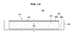
- the bottom chassis 40 is formed as a sandwich panel 41 including a plastic core 42 provided inside a planar material 43.
- the plastic core 42 is sandwiched between two planar material layers 43.
- the bottom chassis 40 is formed with the plastic core 42 including a non-conductive heat dissipation member and the planar material 43 including a conductive heat dissipation member.
- the plastic core 42 is a relatively poor conductor of heat and the planar material is a relatively good heat conductor, so that heat is dissipated at the outer planar material layer and not transmitted to the display panel.
- the planar material 43 may include at least one of aluminum, steel, a metal, and a fiber composite material.
- the plastic core 42 may be formed of a plastic material including at least one of polypropylene (PP), polycarbonate (PC), polyethylene (PE), polyurethane (PU), polystyrene (PS), and polyvinyl chloride (PVC).
- PP polypropylene
- PC polycarbonate
- PE polyethylene
- PU polyurethane
- PS polystyrene
- PVC polyvinyl chloride
- the plastic core 42 may be formed of a composite including at least one of glass fibers, whiskers, and a plastic material including at least one of PP, PC, PE, PU, PS, and PVC.
- the plastic core 42 may include a foam which is foamed of a plastic material.
- the planar material 43 is formed in at least one plate shape.
- the planar material 43 may include a first planar material 43a disposed on one side of the plastic core 42 and a second planar material 43b disposed on the other side thereof.
- the bottom chassis 40 may be formed with the sandwich panel 41 in which the plastic core 42 is interposed between the first planar material 43a and the second planar material 43b.
- the sandwich panel 41 may further include an adhesive 44 and an adhesive film for adhesion between the first planar material 43a, the second planar material 43b, and the plastic core 42.
- the adhesive 44 may include an epoxy coating.
- At least one of the planar materials 43 forming the bottom chassis 40 includes a coupler 45 for coupling with the top chassis 20.
- the bottom chassis 40 has the coupler 45 bent to be formed perpendicular to the display panel 11.
- the coupler 45 of the bottom chassis 40 may be coupled with the top chassis 20 by coupling units (not shown) such as screws, hooks, etc.
- the above-described bottom chassis 40 coupled to the display panel 11 may quickly dissipate heat generated through the light emitting diode module 34 of the display module 10 to the outside of the display apparatus 1.
- a jig 50 having a first jig 50a in an upward direction and the second jig 50b in a downward direction corresponding to the first jig 50a is provided.
- the first planar material 43a, the plastic core 42 and the second planar material 43b are sequentially stacked in an upward direction on the second jig 50b.
- the adhesive 44 may be coated between the first planar material 43a and a lower surface of the plastic core 42 and between the second planar material 43b and an upper surface of the plastic core 42.
- the second jig 50b moves in a downward direction and a thermal compression process may be performed.
- the adhesive 44 is coated between the planar material 43 and the plastic core 42, but the aspect of the present invention is not limited thereto.
- a temperature of the plastic core 42 is increased, the plastic core 42 is interposed between the first planar material 43a and the second planar material 43b, and then the sandwich panel 41 may be formed by pressing the jig.
- the plastic core 42 is preferably formed by a pressing process.
- the sandwich panel 41 as fabricated above may be variously formed according to design conditions of the display apparatus 1 by controlling a weight reduction, heat insulating or mechanical characteristics according to the material of the plastic core 42
- the sandwich panel 41 may include a bead or foam form capable of enhancing the strength and hardness thereof through a pressing process.
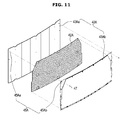
- the sandwich panel 41A may be formed in a curved shape.
- the curved sandwich panel 41A may be formed in a curved shape of which both ends protrude forward compared to the center position.
- the sandwich panel is formed in a curved shape of which both ends protrude forward compared to the center position, but the aspect of the invention is not limited thereto.
- the curved sandwich panel may be formed with different curvatures at both ends.
- the curved sandwich panel 41A may include the planar materials 43 disposed on outer sides of the plastic core 42, and the plastic core 42 interposed and stacked between the planar materials 43.
- the planar materials 43 may include at least one of aluminum, steel, a metal, and a fiber composite material.
- the plastic core 42 may be formed of a plastic material including at least one of PP, PC, PE, PU, PS, and PVC.
- the plastic core 42 may be formed of a composite including at least one of glass fibers, whiskers, and a plastic material including at least one of PP, PC, PE, PU, PS, and PVC.
- the planar materials 43 are formed with at least one plate shape.
- the planar materials 43 may include the first planar material 43a disposed on one side of the plastic core 42 and the second planar material 43b disposed on the other side thereof.
- the curved sandwich panel 41A may be formed with the plastic core 42 interposed between the first planar material 43a and the second planar material 43b.
- the curved sandwich panel 41A has a curved shape of which the center is positioned in a rear direction more than both ends thereof.
- the curved sandwich panel 41A in a curved shape may be formed by pressing the first planar material 43a and the second planar material 43B onto upper and lower surfaces of the plastic core 42 formed in a curved shape by a pressing process.
- the curved sandwich panel 41A as fabricated above has a center thickness t1 greater than a thickness t2 of each of the both ends. In contrast, formation of the center thickness t1 smaller than the thickness t2 of each of the both ends is possible.
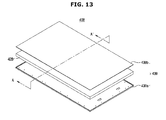
- the sandwich panel 41B may include a plurality of regions 41Ba, 41Bb, and 41Bc having different areas from each other in a single plate.
- the sandwich panel 41B may include the first region 41Ba, the second region 41Bb connected to the first region 41Ba, and the third region 41Bc connected to the second region 41Bb.
- sloped surfaces 41Bd having a predetermined slope may be provided between the first region 41Ba, the second region 41Bb and the third region 41Bc.
- the sloped surfaces 41Bd are formed by the first region 41Ba, the second region 41Bb, and the third region 41Bc having different heights and thicknesses from each other.
- first region 41Ba, the second region 41Bb, and the third region 41Bc may be located at different positions due to the sloped surfaces 41Bd.
- first region 41Ba, the second region 41Bb, and the third region 41Bc may be formed to have different thicknesses t3 and t4.
- the thickness t3 of the first region 41Ba and the third region 41Bc may be formed to be smaller than the thickness t4 of the second region 41Bb.
- the thickness t3 of the first region 41Ba is formed smaller than the thickness t4 of the second region 41Bb, but the aspect of the invention is not limited thereto.
- the thickness of the first region 41Ba may be formed to greater than that of the second region 41Bb.
- the sandwich panels 41, 41A, and 41B are formed to have various shapes and thicknesses, the formability of the bottom chassis 40 is enhanced.
- the display apparatus 1A includes a display module 10A having a self-emitting type display device that emits light by electrically exciting fluorescent organic compounds, such as an OLED, and a case 2A disposed on an outer side of the display module 10A which protects the display module 10A and inside electrical components.
- a display module 10A having a self-emitting type display device that emits light by electrically exciting fluorescent organic compounds, such as an OLED, and a case 2A disposed on an outer side of the display module 10A which protects the display module 10A and inside electrical components.
- the display module 10A includes a display panel 11A through which an image is displayed, the top chassis 20A which covers edges of a front surface of the display panel 11A, and the bottom chassis 40A which supports a rear surface of the display panel 11A.
- the display panel 11A is formed with the organic light emitting diode panel and the organic light emitting diode panel is easily bent because it is formed with a flexible film form.
- the top chassis 20A may support the edges of the front surface of the display panel 11A so that the display panel 11A maintains in a state installed on the bottom chassis 40A.
- a heat dissipating sheet 12A may be installed on the rear surface of the display panel 11A to quickly disperse and dissipate heat generated from the display panel 11A.
- the bottom chassis 40A may be disposed between the rear surface of the display panel 11A and the case 2A.
- the bottom chassis 40A may be formed in a smaller size than the display panel 11A to correspond to at least a portion of the rear surface of the display panel 11A.
- the bottom chassis 40A may include a planar materials 43A disposed on outer sides of a plastic core 42A and the plastic core 42A interposed and stacked between the planar materials 43A.
- the planar materials 43 may include at least one of aluminum, steel, a metal, and a fiber composite material.
- the plastic core 42A may be formed of a plastic material including at least one of PP, PC, PE, PU, PS, PVC.
- the plastic core 42A may be formed of a composite including at least one of glass fibers, whiskers, and a plastic material including at least one of PP, PC, PE, PU, PS, and PVC.
- the planar materials 43A are formed with at least one plate shape.
- the planar materials 43A may include the first planar material 43Aa disposed on one side of the plastic core 42A and the second planar material 43Ab disposed on the other side thereof.
- the curved sandwich panel may be formed with the plastic core 42A interposed between the first planar material 43Aa and the second planar material 43Ab.
- the first planar material 43Aa and the second planar material 43Ab have a size corresponding to the rear surface of the display panel 11A.
- Fixing holes 45A may be formed in edges of the first planar material 43Aa and the second planar material 43Ab for coupling with each other.
- the fixing holes 45A may include at least one first fixing hole 45Aa formed to be separated by predetermined intervals in the edges of the first planar material 43Aa and at least one second fixing hole 45Ab formed in edges of the second planar material 43Ab to corresponding to the first fixing hole 45Aa.
- the plastic core 42A may be formed smaller than the first planar material 43Aa and the second planar material 43Ab.
- the plastic core 42A is disposed between the first planar material 43Aa and the second planar material 43ab and the bottom chassis 40A may be formed with the sandwich panel coupled by a fixing member 47 which passes through the first fixing hole 45Aa and the second fixing hole 45Ab in the edges of the first planar material 43Aa and the second planar material 43Ab.
- the plastic core 42A and the sandwich panel is formed by coupling the first planar material 43Aa and the second planar material 43Ab by the fixing member 47, but the aspect of the present is not limited thereto.
- the planar material 43A and the plastic core 42A may be adhered by an adhesive.
- a display apparatus 1B in accordance with another embodiment of the present invention includes a display module 10B for displaying image information, and a case 2B disposed on outer sides of a display module 10B and provided to protect the display module 10B and inside electrical components.
- the case 2B is disposed to cover a rear surface of the display module 10B.
- the case 2B may be detachably coupled with the display module 10B.
- the display module 10B may include a display panel 11B formed with a liquid crystal panel, a backlight unit 30B separately disposed in the rear of the display panel 11B and provided so that light thereof is incident to the display panel 11B, a middle mold frame 21B which supports the display panel 11B and the backlight unit 30B components to be spaced apart from each other, a top chassis 20B and a bottom chassis 40B respectively disposed in front of the display panel 11 and in the rear of the backlight unit 30B.
- the display panel 11B may be formed with a plate in a planar shape.
- the display panel 11B may form images by controlling the orientation of a liquid crystal layer, but may display images using light provided by the backlight unit 30B disposed on the rear surface of the display panel 11B due to no self-emitting.
- the backlight unit 30B is formed to include a plurality of optical sheets 33B disposed in the rear of the display panel 11B, a light guide plate 31B disposed in the rear of the optical sheet 33B, a reflective sheet 32B disposed on the rear surface of the light guide plate 31B, a light emitting diode module 34B for supplying light to the light guide plate 31B.
- the bottom chassis 40B is disposed in the rear of the backlight unit 30B and may be formed to accommodate the backlight unit 30B.
- the bottom chassis 40B may include planar materials 43B disposed on outer sides of the plastic core 42B and a plastic core 42B interposed and stacked between the planar materials 43B.
- the planar material 43B may include at least one of aluminum, steel, a metal, and a fiber composite material.
- the plastic core 42B may be formed of a plastic material including at least one of PP, PC, PE, PU, PS, and PVC.
- the plastic core 42B may be formed of a composite including at least one of glass fibers, whiskers, and a plastic material including at least one of PP, PC, PE, PU, PS, and PVC.
- the planar materials 43B are formed with at least one plate shape.
- the planar materials 43B may include the first planar material 43Ba disposed on the front surface of the plastic core 42B and the second planar material 43Bb on the rear surface of the plastic core 42B.
- the curved sandwich panel may be formed with the plastic core 42B interposed between the first planar material 43Ba and the second planar material 43Bb.
- the sandwich panel may be formed by a pressing process.
- the planar materials 43B and the plastic core 42B may be adhered by an adhesive.
- the adhesive 44B adhering the first planar material 43Ba, the second planar material 43Bb, and the plastic core 42B may include an epoxy coating.
- the bottom chassis 40B has a coupler 45B formed to be bent perpendicular to the display panel 11B.
- the coupler 45B is formed to protrude in a direction of the display panel 11B, that is, in a front direction, and may be assembled with the top chassis 20B by coupling units (not shown) such as screws, hooks, etc.
- the display apparatus can be slim and lightweight by the chassis having the sandwich structure to which the plastic core is applied.
- the display apparatus has an advantage for securing the strength and hardness of the bottom chassis.
Landscapes
- Physics & Mathematics (AREA)
- Nonlinear Science (AREA)
- General Physics & Mathematics (AREA)
- Optics & Photonics (AREA)
- Mathematical Physics (AREA)
- Chemical & Material Sciences (AREA)
- Crystallography & Structural Chemistry (AREA)
- Engineering & Computer Science (AREA)
- Microelectronics & Electronic Packaging (AREA)
- Thermal Sciences (AREA)
- Theoretical Computer Science (AREA)
- Devices For Indicating Variable Information By Combining Individual Elements (AREA)
- Liquid Crystal (AREA)
Applications Claiming Priority (1)
| Application Number | Priority Date | Filing Date | Title |
|---|---|---|---|
| KR1020140146105A KR102301373B1 (ko) | 2014-10-27 | 2014-10-27 | 디스플레이 장치 |
Publications (2)
| Publication Number | Publication Date |
|---|---|
| EP3015909A1 true EP3015909A1 (de) | 2016-05-04 |
| EP3015909B1 EP3015909B1 (de) | 2021-02-17 |
Family
ID=54360182
Family Applications (1)
| Application Number | Title | Priority Date | Filing Date |
|---|---|---|---|
| EP15191309.2A Active EP3015909B1 (de) | 2014-10-27 | 2015-10-23 | Anzeigevorrichtung |
Country Status (5)
| Country | Link |
|---|---|
| US (3) | US10349534B2 (de) |
| EP (1) | EP3015909B1 (de) |
| KR (2) | KR102301373B1 (de) |
| CN (1) | CN105549243A (de) |
| WO (1) | WO2016068549A1 (de) |
Families Citing this family (13)
| Publication number | Priority date | Publication date | Assignee | Title |
|---|---|---|---|---|
| CN107329301B (zh) * | 2016-04-29 | 2020-10-16 | 群创光电股份有限公司 | 显示装置 |
| KR20190102983A (ko) * | 2017-01-17 | 2019-09-04 | 세키스이가가쿠 고교가부시키가이샤 | 충전 접합재, 보호 시트 부착 충전 접합재, 적층체, 광학 디바이스 및 광학 디바이스용 보호 패널 |
| KR102285031B1 (ko) * | 2017-08-01 | 2021-08-02 | 엘지디스플레이 주식회사 | 표시장치 |
| EP3678367B1 (de) * | 2017-08-28 | 2023-12-13 | LG Electronics Inc. | Anzeigevorrichtung |
| KR102380884B1 (ko) * | 2017-09-11 | 2022-03-31 | 삼성전자주식회사 | 디스플레이 모듈 및 이를 갖는 디스플레이 장치 |
| US20190291502A1 (en) * | 2018-03-20 | 2019-09-26 | Microsoft Technology Licensing, Llc | Forming a non-planar composite |
| KR102544326B1 (ko) * | 2018-08-27 | 2023-06-19 | 삼성디스플레이 주식회사 | 표시 장치 |
| US10923002B1 (en) * | 2019-08-29 | 2021-02-16 | Wuhan China Star Optoelectronics Semiconductor Display Technology Co., Ltd. | Flexible display device |
| WO2022109924A1 (zh) * | 2020-11-26 | 2022-06-02 | 东莞市豪顺精密科技有限公司 | 一种用于显示器的卷边钢塑背板及其制造方法 |
| KR102475579B1 (ko) * | 2020-12-29 | 2022-12-07 | 엘지디스플레이 주식회사 | 표시장치 |
| CN113554944B (zh) * | 2021-07-01 | 2023-02-03 | 东莞市豪顺精密科技有限公司 | 一种超薄显示面板组件及其制造方法 |
| KR20230080962A (ko) * | 2021-11-30 | 2023-06-07 | 삼성전자주식회사 | 디스플레이 장치 |
| KR20230122929A (ko) * | 2022-02-15 | 2023-08-22 | 엘지전자 주식회사 | 디스플레이 디바이스 |
Citations (6)
| Publication number | Priority date | Publication date | Assignee | Title |
|---|---|---|---|---|
| EP0019835A1 (de) * | 1979-05-21 | 1980-12-10 | The Dow Chemical Company | Verformbare Metall-Kunststoff-Metall-Schichtstoffe und Verfahren zu deren Herstellung |
| EP0078174A2 (de) * | 1981-10-28 | 1983-05-04 | Sumitomo Chemical Company, Limited | Verfahren zur Herstellung von metallthermoplastischem Kunststoff-Metall-Sandwichschichtstoff |
| EP0115103A1 (de) * | 1983-01-24 | 1984-08-08 | Sumitomo Metal Industries, Ltd. | Metall-Kunststoff-Metall-Sandwichschichtstoffe die sich bearbeiten lassen |
| CA2819229A1 (en) * | 2010-11-29 | 2012-06-07 | Gtm-Advanced Products B.V. | Metal sheet - fiber reinforced composite laminate |
| EP2730968A2 (de) * | 2012-11-09 | 2014-05-14 | Samsung Electronics Co., Ltd | Gekrümmte Anzeigevorrichtung |
| US20140307474A1 (en) * | 2013-04-11 | 2014-10-16 | Samsung Display Co., Ltd. | Display device |
Family Cites Families (24)
| Publication number | Priority date | Publication date | Assignee | Title |
|---|---|---|---|---|
| US4284447A (en) * | 1976-02-20 | 1981-08-18 | Dickens Luther I | Method of manufacturing a composite panel |
| NL7808115A (nl) * | 1977-08-23 | 1979-02-27 | Ishikawa Takashi | Werkwijze voor het vervaardigen van een bouwpaneel en bouwpaneel. |
| DE3113428A1 (de) * | 1980-08-18 | 1982-04-01 | Schweizerische Aluminium AG, 3965 Chippis | Verfahren zur herstellung einer metall-kunststoffverbundfolie sowie eine nach dem verfahren hergestellte verbundfolie |
| US4671985A (en) * | 1984-11-05 | 1987-06-09 | Swiss Aluminium Ltd. | Thin, deformable composite laminate |
| US4941074A (en) * | 1988-12-29 | 1990-07-10 | Road Rescue, Inc. | Light boxes |
| US5461548A (en) * | 1994-04-11 | 1995-10-24 | Esslinger; James T. | Fiber optic backlight illumination panel for graphics/logos on a moving vehicle |
| US6455148B1 (en) * | 2000-07-07 | 2002-09-24 | Reynolds Metals Company | Composite panel with a foamed plastic core |
| US7222977B1 (en) * | 2002-04-10 | 2007-05-29 | Blue Ridge International Products Company | Light and sound mirror assembly with appearing characters |
| WO2006082595A1 (en) * | 2005-02-02 | 2006-08-10 | Defence Research & Development Organisation | Lightweight structural composite for load bearing application |
| KR20060095725A (ko) | 2005-02-28 | 2006-09-01 | 삼성에스디아이 주식회사 | 디스플레이 모듈 |
| KR20060102007A (ko) | 2005-03-22 | 2006-09-27 | 삼성에스디아이 주식회사 | 샤시 베이스 조립체와, 이를 채용한 플라즈마 표시장치조립체 |
| JP4661735B2 (ja) * | 2005-09-21 | 2011-03-30 | 日本ビクター株式会社 | 面光源装置 |
| US20070209317A1 (en) * | 2006-03-10 | 2007-09-13 | Jensen Gary L | Thermal transfer barrier building members |
| US8184832B2 (en) * | 2006-04-14 | 2012-05-22 | Harman Murray R | Electrostatic loudspeaker capable of dispersing sound both horizontally and vertically |
| US8147086B2 (en) * | 2007-02-16 | 2012-04-03 | Tait Cynthia K | Purselight with touch-sensitive switch |
| JP2008304535A (ja) * | 2007-06-05 | 2008-12-18 | Hitachi Displays Ltd | 表示装置 |
| KR101418585B1 (ko) * | 2007-12-10 | 2014-07-16 | 삼성디스플레이 주식회사 | 백라이트 어셈블리, 이를 포함하는 표시 장치 및 이의 조립방법 |
| US20090308521A1 (en) * | 2008-06-12 | 2009-12-17 | High Impact Technology, L.L.C. | Compression-selective sheet-material density and thickness and methodology |
| US8469569B1 (en) * | 2009-09-26 | 2013-06-25 | William Loftus Tunnicliffe | Illuminated sports board utilizing a battery or self-powered internal light source that is transmitted through the clear interior of the board in order to illuminate the board and any light altering elements contained in, or applied to, the board |
| KR101203053B1 (ko) | 2010-06-08 | 2012-11-20 | 아주스틸 주식회사 | 엘이디 텔레비젼용 고 방열성 알루미늄 라미네이팅 바텀 샤시 및 제조방법 |
| US9081126B2 (en) * | 2010-11-29 | 2015-07-14 | Sharp Kabushiki Kaisha | Illumination device, display device, and television reception device |
| US8988628B2 (en) | 2011-06-23 | 2015-03-24 | Apple Inc. | Coated chassis for liquid crystal display |
| KR102041883B1 (ko) * | 2012-07-09 | 2019-11-08 | 삼성디스플레이 주식회사 | 커브드 프레임 및 이를 갖는 커브드 표시장치 |
| KR101450207B1 (ko) | 2012-09-24 | 2014-10-14 | 홍성산업 주식회사 | 디스플레이장치용 경량 방열판 |
-
2014
- 2014-10-27 KR KR1020140146105A patent/KR102301373B1/ko active IP Right Grant
-
2015
- 2015-10-21 US US14/919,173 patent/US10349534B2/en active Active
- 2015-10-23 EP EP15191309.2A patent/EP3015909B1/de active Active
- 2015-10-23 WO PCT/KR2015/011268 patent/WO2016068549A1/en active Application Filing
- 2015-10-27 CN CN201510707100.2A patent/CN105549243A/zh active Pending
-
2019
- 2019-05-24 US US16/421,961 patent/US10582624B2/en active Active
-
2020
- 2020-01-30 US US16/777,002 patent/US10798832B2/en active Active
-
2021
- 2021-07-14 KR KR1020210092311A patent/KR102339541B1/ko active IP Right Grant
Patent Citations (6)
| Publication number | Priority date | Publication date | Assignee | Title |
|---|---|---|---|---|
| EP0019835A1 (de) * | 1979-05-21 | 1980-12-10 | The Dow Chemical Company | Verformbare Metall-Kunststoff-Metall-Schichtstoffe und Verfahren zu deren Herstellung |
| EP0078174A2 (de) * | 1981-10-28 | 1983-05-04 | Sumitomo Chemical Company, Limited | Verfahren zur Herstellung von metallthermoplastischem Kunststoff-Metall-Sandwichschichtstoff |
| EP0115103A1 (de) * | 1983-01-24 | 1984-08-08 | Sumitomo Metal Industries, Ltd. | Metall-Kunststoff-Metall-Sandwichschichtstoffe die sich bearbeiten lassen |
| CA2819229A1 (en) * | 2010-11-29 | 2012-06-07 | Gtm-Advanced Products B.V. | Metal sheet - fiber reinforced composite laminate |
| EP2730968A2 (de) * | 2012-11-09 | 2014-05-14 | Samsung Electronics Co., Ltd | Gekrümmte Anzeigevorrichtung |
| US20140307474A1 (en) * | 2013-04-11 | 2014-10-16 | Samsung Display Co., Ltd. | Display device |
Also Published As
| Publication number | Publication date |
|---|---|
| US20200170130A1 (en) | 2020-05-28 |
| KR20210093805A (ko) | 2021-07-28 |
| CN105549243A (zh) | 2016-05-04 |
| KR102339541B1 (ko) | 2021-12-16 |
| US10349534B2 (en) | 2019-07-09 |
| US20190281709A1 (en) | 2019-09-12 |
| KR20160049272A (ko) | 2016-05-09 |
| US10798832B2 (en) | 2020-10-06 |
| US20160120043A1 (en) | 2016-04-28 |
| EP3015909B1 (de) | 2021-02-17 |
| US10582624B2 (en) | 2020-03-03 |
| KR102301373B1 (ko) | 2021-09-14 |
| WO2016068549A1 (en) | 2016-05-06 |
Similar Documents
| Publication | Publication Date | Title |
|---|---|---|
| US10798832B2 (en) | Display apparatus | |
| US9535208B2 (en) | Bendable display apparatus having a guide unit which guides a light guide plate | |
| EP3054341B1 (de) | Anzeigevorrichtung | |
| CN107065257B (zh) | 显示装置 | |
| US9632237B2 (en) | Illumination device, display device, and TV receiver | |
| US10581013B2 (en) | Display module and display apparatus having the same | |
| EP2920781B1 (de) | Anzeigevorrichtung | |
| US8616737B2 (en) | Backlight assembly and display apparatus having the same | |
| KR101577336B1 (ko) | 곡면 디스플레이 장치 | |
| US20140036197A1 (en) | Liquid Crystal Module and Liquid Crystal Display Device | |
| KR20150066021A (ko) | 백커버를 가지는 박형 디스플레이 장치 | |
| KR20200130598A (ko) | 광 믹싱 공간을 갖는 디스플레이 장치 | |
| US10935226B2 (en) | Lighting device and display apparatus | |
| WO2012039397A1 (ja) | 発光装置、照明装置および表示装置 |
Legal Events
| Date | Code | Title | Description |
|---|---|---|---|
| PUAI | Public reference made under article 153(3) epc to a published international application that has entered the european phase |
Free format text: ORIGINAL CODE: 0009012 |
|
| AK | Designated contracting states |
Kind code of ref document: A1 Designated state(s): AL AT BE BG CH CY CZ DE DK EE ES FI FR GB GR HR HU IE IS IT LI LT LU LV MC MK MT NL NO PL PT RO RS SE SI SK SM TR |
|
| AX | Request for extension of the european patent |
Extension state: BA ME |
|
| STAA | Information on the status of an ep patent application or granted ep patent |
Free format text: STATUS: REQUEST FOR EXAMINATION WAS MADE |
|
| 17P | Request for examination filed |
Effective date: 20161104 |
|
| RBV | Designated contracting states (corrected) |
Designated state(s): AL AT BE BG CH CY CZ DE DK EE ES FI FR GB GR HR HU IE IS IT LI LT LU LV MC MK MT NL NO PL PT RO RS SE SI SK SM TR |
|
| STAA | Information on the status of an ep patent application or granted ep patent |
Free format text: STATUS: EXAMINATION IS IN PROGRESS |
|
| 17Q | First examination report despatched |
Effective date: 20180511 |
|
| GRAP | Despatch of communication of intention to grant a patent |
Free format text: ORIGINAL CODE: EPIDOSNIGR1 |
|
| STAA | Information on the status of an ep patent application or granted ep patent |
Free format text: STATUS: GRANT OF PATENT IS INTENDED |
|
| RIC1 | Information provided on ipc code assigned before grant |
Ipc: B32B 15/08 20060101ALI20201001BHEP Ipc: B32B 27/40 20060101ALN20201001BHEP Ipc: B32B 3/26 20060101ALN20201001BHEP Ipc: B32B 15/14 20060101ALI20201001BHEP Ipc: B32B 27/32 20060101ALN20201001BHEP Ipc: B32B 5/22 20060101ALN20201001BHEP Ipc: B32B 15/20 20060101ALN20201001BHEP Ipc: B32B 27/36 20060101ALN20201001BHEP Ipc: B32B 5/24 20060101ALN20201001BHEP Ipc: B32B 5/26 20060101ALN20201001BHEP Ipc: B32B 7/12 20060101ALN20201001BHEP Ipc: G02F 1/1333 20060101AFI20201001BHEP Ipc: B32B 27/30 20060101ALN20201001BHEP Ipc: B32B 27/12 20060101ALN20201001BHEP Ipc: B32B 15/04 20060101ALN20201001BHEP Ipc: B32B 3/28 20060101ALN20201001BHEP Ipc: B32B 5/02 20060101ALN20201001BHEP Ipc: B32B 27/18 20060101ALN20201001BHEP Ipc: B32B 5/18 20060101ALN20201001BHEP Ipc: B32B 27/06 20060101ALI20201001BHEP |
|
| INTG | Intention to grant announced |
Effective date: 20201019 |
|
| GRAS | Grant fee paid |
Free format text: ORIGINAL CODE: EPIDOSNIGR3 |
|
| GRAA | (expected) grant |
Free format text: ORIGINAL CODE: 0009210 |
|
| STAA | Information on the status of an ep patent application or granted ep patent |
Free format text: STATUS: THE PATENT HAS BEEN GRANTED |
|
| AK | Designated contracting states |
Kind code of ref document: B1 Designated state(s): AL AT BE BG CH CY CZ DE DK EE ES FI FR GB GR HR HU IE IS IT LI LT LU LV MC MK MT NL NO PL PT RO RS SE SI SK SM TR |
|
| REG | Reference to a national code |
Ref country code: GB Ref legal event code: FG4D |
|
| REG | Reference to a national code |
Ref country code: CH Ref legal event code: EP |
|
| REG | Reference to a national code |
Ref country code: DE Ref legal event code: R096 Ref document number: 602015065516 Country of ref document: DE |
|
| REG | Reference to a national code |
Ref country code: AT Ref legal event code: REF Ref document number: 1362227 Country of ref document: AT Kind code of ref document: T Effective date: 20210315 |
|
| REG | Reference to a national code |
Ref country code: IE Ref legal event code: FG4D |
|
| REG | Reference to a national code |
Ref country code: LT Ref legal event code: MG9D |
|
| REG | Reference to a national code |
Ref country code: NL Ref legal event code: MP Effective date: 20210217 |
|
| PG25 | Lapsed in a contracting state [announced via postgrant information from national office to epo] |
Ref country code: PT Free format text: LAPSE BECAUSE OF FAILURE TO SUBMIT A TRANSLATION OF THE DESCRIPTION OR TO PAY THE FEE WITHIN THE PRESCRIBED TIME-LIMIT Effective date: 20210617 Ref country code: LT Free format text: LAPSE BECAUSE OF FAILURE TO SUBMIT A TRANSLATION OF THE DESCRIPTION OR TO PAY THE FEE WITHIN THE PRESCRIBED TIME-LIMIT Effective date: 20210217 Ref country code: GR Free format text: LAPSE BECAUSE OF FAILURE TO SUBMIT A TRANSLATION OF THE DESCRIPTION OR TO PAY THE FEE WITHIN THE PRESCRIBED TIME-LIMIT Effective date: 20210518 Ref country code: FI Free format text: LAPSE BECAUSE OF FAILURE TO SUBMIT A TRANSLATION OF THE DESCRIPTION OR TO PAY THE FEE WITHIN THE PRESCRIBED TIME-LIMIT Effective date: 20210217 Ref country code: HR Free format text: LAPSE BECAUSE OF FAILURE TO SUBMIT A TRANSLATION OF THE DESCRIPTION OR TO PAY THE FEE WITHIN THE PRESCRIBED TIME-LIMIT Effective date: 20210217 Ref country code: NO Free format text: LAPSE BECAUSE OF FAILURE TO SUBMIT A TRANSLATION OF THE DESCRIPTION OR TO PAY THE FEE WITHIN THE PRESCRIBED TIME-LIMIT Effective date: 20210517 Ref country code: BG Free format text: LAPSE BECAUSE OF FAILURE TO SUBMIT A TRANSLATION OF THE DESCRIPTION OR TO PAY THE FEE WITHIN THE PRESCRIBED TIME-LIMIT Effective date: 20210517 |
|
| REG | Reference to a national code |
Ref country code: AT Ref legal event code: MK05 Ref document number: 1362227 Country of ref document: AT Kind code of ref document: T Effective date: 20210217 |
|
| PG25 | Lapsed in a contracting state [announced via postgrant information from national office to epo] |
Ref country code: LV Free format text: LAPSE BECAUSE OF FAILURE TO SUBMIT A TRANSLATION OF THE DESCRIPTION OR TO PAY THE FEE WITHIN THE PRESCRIBED TIME-LIMIT Effective date: 20210217 Ref country code: RS Free format text: LAPSE BECAUSE OF FAILURE TO SUBMIT A TRANSLATION OF THE DESCRIPTION OR TO PAY THE FEE WITHIN THE PRESCRIBED TIME-LIMIT Effective date: 20210217 Ref country code: PL Free format text: LAPSE BECAUSE OF FAILURE TO SUBMIT A TRANSLATION OF THE DESCRIPTION OR TO PAY THE FEE WITHIN THE PRESCRIBED TIME-LIMIT Effective date: 20210217 Ref country code: NL Free format text: LAPSE BECAUSE OF FAILURE TO SUBMIT A TRANSLATION OF THE DESCRIPTION OR TO PAY THE FEE WITHIN THE PRESCRIBED TIME-LIMIT Effective date: 20210217 Ref country code: SE Free format text: LAPSE BECAUSE OF FAILURE TO SUBMIT A TRANSLATION OF THE DESCRIPTION OR TO PAY THE FEE WITHIN THE PRESCRIBED TIME-LIMIT Effective date: 20210217 |
|
| PG25 | Lapsed in a contracting state [announced via postgrant information from national office to epo] |
Ref country code: IS Free format text: LAPSE BECAUSE OF FAILURE TO SUBMIT A TRANSLATION OF THE DESCRIPTION OR TO PAY THE FEE WITHIN THE PRESCRIBED TIME-LIMIT Effective date: 20210617 |
|
| PG25 | Lapsed in a contracting state [announced via postgrant information from national office to epo] |
Ref country code: EE Free format text: LAPSE BECAUSE OF FAILURE TO SUBMIT A TRANSLATION OF THE DESCRIPTION OR TO PAY THE FEE WITHIN THE PRESCRIBED TIME-LIMIT Effective date: 20210217 Ref country code: CZ Free format text: LAPSE BECAUSE OF FAILURE TO SUBMIT A TRANSLATION OF THE DESCRIPTION OR TO PAY THE FEE WITHIN THE PRESCRIBED TIME-LIMIT Effective date: 20210217 Ref country code: AT Free format text: LAPSE BECAUSE OF FAILURE TO SUBMIT A TRANSLATION OF THE DESCRIPTION OR TO PAY THE FEE WITHIN THE PRESCRIBED TIME-LIMIT Effective date: 20210217 Ref country code: SM Free format text: LAPSE BECAUSE OF FAILURE TO SUBMIT A TRANSLATION OF THE DESCRIPTION OR TO PAY THE FEE WITHIN THE PRESCRIBED TIME-LIMIT Effective date: 20210217 |
|
| REG | Reference to a national code |
Ref country code: DE Ref legal event code: R097 Ref document number: 602015065516 Country of ref document: DE |
|
| PG25 | Lapsed in a contracting state [announced via postgrant information from national office to epo] |
Ref country code: DK Free format text: LAPSE BECAUSE OF FAILURE TO SUBMIT A TRANSLATION OF THE DESCRIPTION OR TO PAY THE FEE WITHIN THE PRESCRIBED TIME-LIMIT Effective date: 20210217 Ref country code: ES Free format text: LAPSE BECAUSE OF FAILURE TO SUBMIT A TRANSLATION OF THE DESCRIPTION OR TO PAY THE FEE WITHIN THE PRESCRIBED TIME-LIMIT Effective date: 20210217 Ref country code: SK Free format text: LAPSE BECAUSE OF FAILURE TO SUBMIT A TRANSLATION OF THE DESCRIPTION OR TO PAY THE FEE WITHIN THE PRESCRIBED TIME-LIMIT Effective date: 20210217 Ref country code: RO Free format text: LAPSE BECAUSE OF FAILURE TO SUBMIT A TRANSLATION OF THE DESCRIPTION OR TO PAY THE FEE WITHIN THE PRESCRIBED TIME-LIMIT Effective date: 20210217 |
|
| PLBE | No opposition filed within time limit |
Free format text: ORIGINAL CODE: 0009261 |
|
| STAA | Information on the status of an ep patent application or granted ep patent |
Free format text: STATUS: NO OPPOSITION FILED WITHIN TIME LIMIT |
|
| 26N | No opposition filed |
Effective date: 20211118 |
|
| PG25 | Lapsed in a contracting state [announced via postgrant information from national office to epo] |
Ref country code: AL Free format text: LAPSE BECAUSE OF FAILURE TO SUBMIT A TRANSLATION OF THE DESCRIPTION OR TO PAY THE FEE WITHIN THE PRESCRIBED TIME-LIMIT Effective date: 20210217 |
|
| PG25 | Lapsed in a contracting state [announced via postgrant information from national office to epo] |
Ref country code: SI Free format text: LAPSE BECAUSE OF FAILURE TO SUBMIT A TRANSLATION OF THE DESCRIPTION OR TO PAY THE FEE WITHIN THE PRESCRIBED TIME-LIMIT Effective date: 20210217 |
|
| PG25 | Lapsed in a contracting state [announced via postgrant information from national office to epo] |
Ref country code: IT Free format text: LAPSE BECAUSE OF FAILURE TO SUBMIT A TRANSLATION OF THE DESCRIPTION OR TO PAY THE FEE WITHIN THE PRESCRIBED TIME-LIMIT Effective date: 20210217 |
|
| REG | Reference to a national code |
Ref country code: CH Ref legal event code: PL |
|
| PG25 | Lapsed in a contracting state [announced via postgrant information from national office to epo] |
Ref country code: IS Free format text: LAPSE BECAUSE OF FAILURE TO SUBMIT A TRANSLATION OF THE DESCRIPTION OR TO PAY THE FEE WITHIN THE PRESCRIBED TIME-LIMIT Effective date: 20210617 |
|
| REG | Reference to a national code |
Ref country code: BE Ref legal event code: MM Effective date: 20211031 |
|
| PG25 | Lapsed in a contracting state [announced via postgrant information from national office to epo] |
Ref country code: MC Free format text: LAPSE BECAUSE OF FAILURE TO SUBMIT A TRANSLATION OF THE DESCRIPTION OR TO PAY THE FEE WITHIN THE PRESCRIBED TIME-LIMIT Effective date: 20210217 |
|
| PG25 | Lapsed in a contracting state [announced via postgrant information from national office to epo] |
Ref country code: LU Free format text: LAPSE BECAUSE OF NON-PAYMENT OF DUE FEES Effective date: 20211023 Ref country code: BE Free format text: LAPSE BECAUSE OF NON-PAYMENT OF DUE FEES Effective date: 20211031 |
|
| PG25 | Lapsed in a contracting state [announced via postgrant information from national office to epo] |
Ref country code: LI Free format text: LAPSE BECAUSE OF NON-PAYMENT OF DUE FEES Effective date: 20211031 Ref country code: CH Free format text: LAPSE BECAUSE OF NON-PAYMENT OF DUE FEES Effective date: 20211031 |
|
| PG25 | Lapsed in a contracting state [announced via postgrant information from national office to epo] |
Ref country code: FR Free format text: LAPSE BECAUSE OF NON-PAYMENT OF DUE FEES Effective date: 20211031 |
|
| PG25 | Lapsed in a contracting state [announced via postgrant information from national office to epo] |
Ref country code: IE Free format text: LAPSE BECAUSE OF NON-PAYMENT OF DUE FEES Effective date: 20211023 |
|
| PG25 | Lapsed in a contracting state [announced via postgrant information from national office to epo] |
Ref country code: HU Free format text: LAPSE BECAUSE OF FAILURE TO SUBMIT A TRANSLATION OF THE DESCRIPTION OR TO PAY THE FEE WITHIN THE PRESCRIBED TIME-LIMIT; INVALID AB INITIO Effective date: 20151023 |
|
| PG25 | Lapsed in a contracting state [announced via postgrant information from national office to epo] |
Ref country code: CY Free format text: LAPSE BECAUSE OF FAILURE TO SUBMIT A TRANSLATION OF THE DESCRIPTION OR TO PAY THE FEE WITHIN THE PRESCRIBED TIME-LIMIT Effective date: 20210217 |
|
| PGFP | Annual fee paid to national office [announced via postgrant information from national office to epo] |
Ref country code: GB Payment date: 20230920 Year of fee payment: 9 |
|
| PGFP | Annual fee paid to national office [announced via postgrant information from national office to epo] |
Ref country code: DE Payment date: 20230920 Year of fee payment: 9 |
|
| PG25 | Lapsed in a contracting state [announced via postgrant information from national office to epo] |
Ref country code: MK Free format text: LAPSE BECAUSE OF FAILURE TO SUBMIT A TRANSLATION OF THE DESCRIPTION OR TO PAY THE FEE WITHIN THE PRESCRIBED TIME-LIMIT Effective date: 20210217 |