EP3014288B1 - Stromdetektorschaltung - Google Patents
Stromdetektorschaltung Download PDFInfo
- Publication number
- EP3014288B1 EP3014288B1 EP13887623.0A EP13887623A EP3014288B1 EP 3014288 B1 EP3014288 B1 EP 3014288B1 EP 13887623 A EP13887623 A EP 13887623A EP 3014288 B1 EP3014288 B1 EP 3014288B1
- Authority
- EP
- European Patent Office
- Prior art keywords
- voltage
- power
- circuit
- coupled
- loadline
- Prior art date
- Legal status (The legal status is an assumption and is not a legal conclusion. Google has not performed a legal analysis and makes no representation as to the accuracy of the status listed.)
- Active
Links
Images




Classifications
-
- G—PHYSICS
- G01—MEASURING; TESTING
- G01R—MEASURING ELECTRIC VARIABLES; MEASURING MAGNETIC VARIABLES
- G01R19/00—Arrangements for measuring currents or voltages or for indicating presence or sign thereof
- G01R19/30—Measuring the maximum or the minimum value of current or voltage reached in a time interval
-
- G—PHYSICS
- G06—COMPUTING OR CALCULATING; COUNTING
- G06F—ELECTRIC DIGITAL DATA PROCESSING
- G06F1/00—Details not covered by groups G06F3/00 - G06F13/00 and G06F21/00
- G06F1/16—Constructional details or arrangements
- G06F1/20—Cooling means
-
- G—PHYSICS
- G01—MEASURING; TESTING
- G01R—MEASURING ELECTRIC VARIABLES; MEASURING MAGNETIC VARIABLES
- G01R19/00—Arrangements for measuring currents or voltages or for indicating presence or sign thereof
- G01R19/0084—Measuring voltage only
-
- G—PHYSICS
- G06—COMPUTING OR CALCULATING; COUNTING
- G06F—ELECTRIC DIGITAL DATA PROCESSING
- G06F1/00—Details not covered by groups G06F3/00 - G06F13/00 and G06F21/00
- G06F1/26—Power supply means, e.g. regulation thereof
- G06F1/32—Means for saving power
- G06F1/3203—Power management, i.e. event-based initiation of a power-saving mode
- G06F1/3206—Monitoring of events, devices or parameters that trigger a change in power modality
- G06F1/3209—Monitoring remote activity, e.g. over telephone lines or network connections
-
- G—PHYSICS
- G06—COMPUTING OR CALCULATING; COUNTING
- G06F—ELECTRIC DIGITAL DATA PROCESSING
- G06F1/00—Details not covered by groups G06F3/00 - G06F13/00 and G06F21/00
- G06F1/26—Power supply means, e.g. regulation thereof
- G06F1/32—Means for saving power
- G06F1/3203—Power management, i.e. event-based initiation of a power-saving mode
- G06F1/3234—Power saving characterised by the action undertaken
- G06F1/324—Power saving characterised by the action undertaken by lowering clock frequency
-
- G—PHYSICS
- G06—COMPUTING OR CALCULATING; COUNTING
- G06F—ELECTRIC DIGITAL DATA PROCESSING
- G06F1/00—Details not covered by groups G06F3/00 - G06F13/00 and G06F21/00
- G06F1/26—Power supply means, e.g. regulation thereof
- G06F1/32—Means for saving power
- G06F1/3203—Power management, i.e. event-based initiation of a power-saving mode
- G06F1/3234—Power saving characterised by the action undertaken
- G06F1/3296—Power saving characterised by the action undertaken by lowering the supply or operating voltage
-
- H—ELECTRICITY
- H03—ELECTRONIC CIRCUITRY
- H03M—CODING; DECODING; CODE CONVERSION IN GENERAL
- H03M1/00—Analogue/digital conversion; Digital/analogue conversion
- H03M1/66—Digital/analogue converters
-
- Y—GENERAL TAGGING OF NEW TECHNOLOGICAL DEVELOPMENTS; GENERAL TAGGING OF CROSS-SECTIONAL TECHNOLOGIES SPANNING OVER SEVERAL SECTIONS OF THE IPC; TECHNICAL SUBJECTS COVERED BY FORMER USPC CROSS-REFERENCE ART COLLECTIONS [XRACs] AND DIGESTS
- Y02—TECHNOLOGIES OR APPLICATIONS FOR MITIGATION OR ADAPTATION AGAINST CLIMATE CHANGE
- Y02D—CLIMATE CHANGE MITIGATION TECHNOLOGIES IN INFORMATION AND COMMUNICATION TECHNOLOGIES [ICT], I.E. INFORMATION AND COMMUNICATION TECHNOLOGIES AIMING AT THE REDUCTION OF THEIR OWN ENERGY USE
- Y02D10/00—Energy efficient computing, e.g. low power processors, power management or thermal management
Definitions
- the number of cores has rapidly increased for each new generation of servers, thanks to a constantly growing need for improved server performance.
- the total power envelope for each generation of servers has not changed. Power management is used to control and reduce power usage so that the server delivers optimal performance and the power supply does not get overloaded.
- a power monitor for use in a computer having a processor.
- the example power monitor includes a current sense resistor associated with a power input of the processor and an amplifier in communication with the current sense resistor to develop a signal representative of power dissipated by the processor.
- the power monitor also includes a comparison circuit to compare the signal output by the amplifier with a predetermined threshold.
- US 2004/0133816 A1 discloses a system for performing power saving control in which a current flowing through an electrical path is detected as a voltage and the voltage is amplified and outputted. When the outputted voltage exceeds a power limit, a power limit detection signal is output and upon receipt of the power limit detection signal, throttling of a clock frequency of the Central Processing Unit (CPU) is performed.
- CPU Central Processing Unit
- Japanese patent application publication number JP H09 289495 A by Matsushita Electric Ind Co Ltd. Discloses an amplifier and an optical receiving circuit that uses a signal generated by the amplifier. Two identical maximum value holding circuits are provided between a first differential amplifier and outputs of the maximum value holding circuits are input to a second differential amplifier. Output variations generated by the two maximum value holding circuits owing to temperature variation are cancelled by the second differential amplifier. A third differential amplifier receives as inputs both an output of the first differential amplifier and an output of the second differential amplifier. The third differential amplifier accurately follows a DC level of the signal input.
- US 2012/0194141 A1 discloses voltage detection by selectably voltage sensing the voltage of a rechargeable battery or current sensing a current flowing through the rechargeable battery.
- US 2004/049704 A1 discloses an apparatus for dynamically adjusting a power consumption of a CPU of a computer system.
- a current flowing through a limiting resistor is detected and compared with a predetermined current and a warning signal is issued when the detected current is larger than the predetermined value. Responsive to the warning signal an asynchronous frequency reduction instruction is sent to the CPU.
- Thermal design power represents the amount of power dissipated when a CPU is running at its nominal frequency while running the highest power real world application.
- Maximum application power represents the maximum amount of power dissipated when the CPU is running non-virus applications, which can occur when the CPU is overclocked or in Turbo.
- Maximum power (P max ) is a power specification that refers to the absolute maximum power dissipated by the CPU during operation.
- a power virus is a malicious computer program that is coded to maximize CPU power dissipation (or thermal energy output), causing the electronic device to overheat over time.
- a power virus can cause the CPU to operate at P max .
- P max can be several times greater than TDP, and may be substantially greater than P app .
- P max is not sustainable by the server platform's power supply.
- a power detector circuit in an electronic device can control the amount of power dissipated by a CPU in operation and reduce thermal output in order to prevent overheating.
- the power detector circuit can measure voltage at a sensing point, and determine if a certain power condition has been reached.
- a power condition can refer to a level of power dissipated by a central processing unit (CPU) during operation. If the power condition has been reached, the power detector circuit can send out an alert to reduce power production. By measuring voltage, the power detector circuit can provide fast feedback (within a few microseconds) that the power condition has been reached.
- the power detector circuit can also be adapted to be used for a number of different electronic device configurations. The power detector circuit can be used to detect when the electronic device is operating under unsustainable conditions, and take action to alleviate the unsustainable conditions.
- Fig. 1 is a block diagram of a system for power management and delivery in an electronic device.
- the system 100 can be used in an electronic device such as a server platform, a computer, a tablet, or a mobile phone.
- the electronic device can utilize a multi-core processor.
- the system 100 includes a central processing unit (CPU) 102 connected to a motherboard 104.
- the CPU 102 is used to run programs and applications, and may contain multiple processor cores 105. In some embodiments, the system 100 will utilize more than one CPU 102.
- a power control unit 106 is configured to deliver power to the one or more processor cores 102.
- the power control unit 106 can control the amount of power delivered to the one or more processor cores 102, and can throttle the one or more processor cores 102 in order to reduce power usage.
- the power control unit 106 can be coupled to or be contained in the CPU 102.
- a power supply 107 can deliver power to the motherboard.
- a power detector circuit 108 can be coupled to the CPU 102 or the power control unit 106.
- the power detector circuit 108 is configured to measure how much power is being produced by the CPU 102 during operation. More specifically, a sensed voltage in the power detector circuit 108 can be measured at a sense point within the power detector circuit 108. In some embodiments, the sense point can be a sensor 109. If the sensed voltage is less than a pre-determined threshold, then the power detector circuit 108 can determine that a certain power condition has been detected. When the power condition has been detected, the power detector circuit 108 can send an alert to the power control unit 106, and command the power control unit 106 to throttle the one or more processor cores 102 to reduce power production.
- the power condition can occur when a threshold of power produced is reached.
- the threshold can be P max , the maximum amount of power produced while a processor core 102 is running a power virus.
- a user can set the threshold at a particular level, e.g. P app .
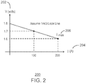
- Fig. 2 is a graph illustrating the relationship between voltage and current in a power detector circuit. As is seen in the graph 200, the voltage 202 is proportional to the current 204.
- the current 204 can be supplied from a voltage regulator to a loadline in a circuit.
- the current 204 can represent the amount of power produced during CPU operation.
- I max 206 represents the current at P max , the maximum amount of power produced while a CPU is running a power virus.
- the loadline of Fig. 2 has a resistance of 1 m ⁇ .
- a motherboard voltage regulator provides a nominal voltage of 1.8 V, which is the voltage of the loadline when no current is present. When the current is at I max (200 A), the voltage in the loadline is 1.6 V.
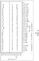
- Fig. 3 is a graph illustrating sensed voltage levels in a power detector circuit for various server platform configurations.
- the graph 300 displays the voltage sensed 302 for platform configurations, also known as skews, at three different current levels using a power detecting circuit.
- Each skew 604 is represented by a series of letters that indicate characteristics of the server platform's components, and a number that represents operating temperature.
- Each component of the server platform may be realistic (indicated by "r"), typical ("t"), slow ("s"), or fast ("f”).
- "typical” represents a CPU part that consists of transistors and interconnects which are deemed typical for the process technology that the CPU is manufactured with.
- the operating temperature may be between 0° C and 110°C.
- the skew "rsss_0.0" indicates a realistic server platform with a slow P transistor, a slow N transistor, a slow processor, and an operating temperature of 0° C.
- the sensed voltage readings 302 at each current level is relatively consistent across the different skews 304. This indicates that the power detecting circuit 108 may be used adaptable for different configurations.
- Fig. 4 is a diagram of an embodiment of a power detector circuit.
- the power detector circuit 400 which is an example of the power detector circuit 108 shown in Fig. 1 , can monitor power production and notify a power control unit 106 if a certain power condition has been reached.
- the power detector circuit 400 is configured for current mode sensing. In current mode sensing, a motherboard voltage regulator (MBVR) 402 supplies currents to a pair of circuit lines in order to cancel out temperature-related variance in the resistance of the circuit lines.
- MBVR motherboard voltage regulator
- the MBVR 402 coupled to a motherboard 104 supplies a first current (I 1 ) 404 to a loadline 406 with a first resistor (R 1 (T)) 408.
- the loadline 406 can represent connection from the MBVR to a CPU 102 in which the first current 404 is provided.
- the resistance value of the first resistor 408 may vary depending on temperature.
- a second line 410 with a second resistor (R 2 (T)) 412 can be coupled to the loadline 406, such that a second current (I 2 ) 414 travels along the second line 410.
- the resistance value of the second resistor 412 may also vary depending on temperature.
- the first resistor 408 and the second resistor 412 may be in close thermal proximity of one another, such that they both experience proportionally similar changes in resistance.
- the loadline 406 and the second line 410 are coupled to an amplifier 416.
- the amplifier 416 can be used to force the voltage across the first resistor 408 and the voltage across the second resistor 412 to be equal.
- the loadline 406 can be connected to the positive input of the amplifier 416, and the second line 410 can be coupled to the negative input of the amplifier 416.
- the amplifier 416 can be a low offset amplifier.
- the output of the amplifier 416 is coupled to a precision resistor (R sense ) 418, which may be coupled to the motherboard 104.
- the sensed voltage (V sense ) across the precision resistor 218 can be measured by the power detector circuit 200 at a sense point 420 nearby.
- the sense point 420 is connected to an input of a comparator 422.
- the other input is connected to a digital-to-analog converter (DAC) 424, which is configured to provide a reference voltage (V ref ) to the comparator 422.
- V ref digital-to-analog converter
- the reference voltage may be the voltage level in which maximum power (P max ) occurs.
- the reference voltage may also be a user-defined voltage level.
- the DAC 424 can be coupled to the motherboard 104 or the power control unit 106.
- the comparator 422 can compare the sensed voltage to the reference voltage.
- a filter 426 coupled to the output of the comparator 422 can detect if the sensed voltage falls below the reference voltage for a sustained amount of time. If the sensed voltage does fall below the reference voltage for a sustained amount of time, the power detector circuit 400 can send an alert to the power control unit 106 that a power condition has been reached, and command the power control unit 106 to throttle or slow down operation in one or more processor cores 102.
- the value of the first current can ultimately be calculated.
- the amplifier 416 forces the voltage across the first resistor 408 and the voltage across the second resistor 412 to be equal.
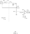
- Fig. 5 is a diagram of an embodiment of a power detector circuit.
- the power detector circuit 500 which is an example of the power detector circuit 108 shown in Fig. 1 , can be configured to power production and notify a power control unit if a certain power condition has been reached.
- the power detector circuit is configured for voltage mode sensing. In voltage mode sensing, a motherboard voltage regulator (MBVR) 402 is used to cancel out temperature-related variance in a circuit line.
- MBVR motherboard voltage regulator
- the MBVR 402 coupled to a motherboard 104 supplies a first current (I 1 ) 404 to a loadline 406 with a first resistor (R 1 (T)) 408.
- the loadline 406 can represent connection from the MBVR to a CPU 102 in which the first current 404 is provided.
- the resistance value of the first resistor 408 may vary depending on temperature.
- the loadline 406 may loop back to the MBVR 402, allowing the MBVR 402 to regulate and cancel any temperature-related changes in the resistance of the first resistor 408.
- the sensed voltage (V sense ) along the loadline 406 can be measured at a sense point 502.
- the sense point 502 is connected to an input of a comparator 422.
- the other input is connected to a digital-to-analog converter (DAC) 424, which is configured to provide a reference voltage (V ref ) to the comparator 422.
- V ref may be the voltage level in which maximum power (P max ) occurs.
- P max maximum power
- the reference voltage may also be a user-defined voltage level.
- the DAC 424 can be coupled to the motherboard 104 or the power control unit 106.
- the comparator 422 can compare the sensed voltage to the reference voltage.
- a filter 426 coupled to the output of the comparator 422 can detect if the sensed voltage falls below the reference voltage for a sustained amount of time. If the sensed voltage does fall below the reference voltage for a sustained amount of time, the power detector circuit 400 can send an alert to the power control unit 106 that a power condition has been reached, and command the power control unit 106 to throttle or slow down operation in one or more processor cores 102.
- the comparator 422 may not be able to accept a high voltage.
- the sensed voltage may be reduced using a voltage divider 504 at the sense point 502.
- the voltage divider 504 may be a resistive divider, a low-pass RC filter, an inductive divider, or a capacitive divider. Accordingly, the reference voltage can be scaled down with the voltage ratio of the voltage divider 504.
- Fig. 6 is a diagram of an embodiment of a power detector circuit.
- the power detector circuit 600 which is an example of the power detector circuit 108 shown in Fig. 1 , can be configured to power production and notify a power control unit if a certain power condition has been reached.
- the power detector circuit is configured to switch between current mode sensing and voltage mode sensing.
- the power detector circuit 600 includes components shown in the circuits illustrated Figs. 4 and 5 , along with a switch 602 that allows the power detector circuit 600 to change between the circuit configured for current mode sensing ( Fig. 4 ) and the circuit configured for voltage mode sensing ( Fig. 5 ).
- Fig. 7 is a diagram of an embodiment of a power detector circuit.
- the power detector circuit 700 which is an example of the power detector circuit 108 shown in Fig. 1 , can monitor power production and notify a power control unit 106 if a certain power condition has been reached.
- the power detector circuit 700 is configured for current mode sensing.
- a motherboard voltage regulator (MBVR) 402 supplies currents to a pair of circuit lines in order to cancel out temperature-related variance in the resistance of the circuit lines.
- the power detector circuit 700 includes components shown in the circuit illustrated in Fig. 4 .
- the power detector circuit further includes an up/down counter 702 coupled to the output of the amplifier 416.
- the up/down counter 702 can compare the voltage from the loadline 406 (referred to herein as V 1 ) to the voltage from the second line 410 (referred to herein as V 2 ). If V 2 is greater than V 1 , the up/down counter 702 can count down in response, and enable transistors to increase the second current I 2 414 such that the value of V 2 is incrementally reduced to be equal to V 1 . If V 2 is less than V 1 , the up/down counter 702 can count up in response, and disable transistors to decrease the second current I 2 414 such that the value of V 2 is incrementally increased to be equal to V 1 .
- Fig. 8 is a diagram of an embodiment of a power detector circuit.
- the power detector circuit 800 which is an example of the power detector circuit 108 shown in Fig. 1 , can monitor power production and notify a power control unit 106 if a certain power condition has been reached.
- the power detector circuit 800 is configured to switch between current mode sensing and voltage mode sensing.
- the power detector circuit 800 includes components shown in the circuit illustrated in Fig. 6 .
- the power detector circuit further includes an up/down counter 702 coupled to the output of the amplifier 416.
- the up/down counter 702 can compare the voltage from the loadline 406 (referred to herein as V 1 ) to the voltage from the second line 410 (referred to herein as V 2 ). If V 2 is greater than V 1 , the up/down counter 702 can count down in response, and enable transistors to increase the second current I 2 414 such that the value of V 2 is incrementally reduced to be equal to V 1 . If V 2 is less than V 1 , the up/down counter 702 can count up in response, and disable transistors to decrease the second current I 2 414 such that the value of V 2 is incrementally increased to be equal to V 1 .
- Fig. 9 is a process flow diagram of a method for detecting maximum power usage.
- the method 900 can be performed by a circuit in an electronic device.
- the circuit determines a sensed voltage at a precision resistor.
- the circuit compares the sensed voltage to a reference voltage.
- the circuit sends an alert that a power condition has been reached in response to determining that the sensed voltage is less than the reference voltage.
- the elements in some cases may each have a same reference number or a different reference number to suggest that the elements represented could be different or similar.
- an element may be flexible enough to have different implementations and work with some or all of the systems shown or described herein.
- the various elements shown in the figures may be the same or different. Which one is referred to as a first element and which is called a second element is arbitrary.
- Coupled may mean that two or more elements are in direct physical or electrical contact. However, “coupled” may also mean that two or more elements are not in direct contact with each other, but yet still co-operate or interact with each other.
- An embodiment is an implementation or example of the inventions.
- Reference in the specification to "an embodiment,” “one embodiment,” “some embodiments,” or “other embodiments” means that a particular feature, structure, or characteristic described in connection with the embodiments is included in at least some embodiments, but not necessarily all embodiments, of the inventions.
- the various appearances “an embodiment,” “one embodiment,” or “some embodiments” are not necessarily all referring to the same embodiments.
Landscapes
- Engineering & Computer Science (AREA)
- Theoretical Computer Science (AREA)
- Physics & Mathematics (AREA)
- General Physics & Mathematics (AREA)
- General Engineering & Computer Science (AREA)
- Human Computer Interaction (AREA)
- Measurement Of Current Or Voltage (AREA)
Claims (11)
- Schaltung zum Verwalten von Leistung und Wärme an einer zentralen Verarbeitungseinheit, umfassend:einen Hauptplatinen-Spannungsregler (402) zum Zuführen eines Stroms zu einer Lastleitung (406);einen Erfassungspunkt (502), gekoppelt an die Lastleitung, wobei die Schaltung eine erfasste Spannung an dem Erfassungspunkt messen soll;einen Komparator (422) zum Vergleichen der erfassten Spannung mit einer Referenzspannung, wobei ein Ausgang des Komparators einen Strompegel, der durch den Hauptplatinen-Spannungsregler bereitgestellt wird, angeben soll; eine zweite Leitung (410), gekoppelt an den Hauptplatinen-Spannungsregler;einen Präzisionswiderstand (418) an dem Erfassungspunkt;einen Verstärker (416) zum Auslöschen einer temperaturbezogenen Variation in dem Widerstand der Lastleitung durch Steuern eines an einen Ausgang des Verstärkers gekoppelten Transistors zum Erhöhen oder Verringern eines Stroms in der zweiten Leitung, wobei die Lastleitung und die zweite Leitung an einen Eingang des Verstärkers gekoppelt sind und der Präzisionswiderstand an den Transistor gekoppelt ist; und einen Schalter (602) zum Wechseln zwischen Spannungsmoduserfassung und Strommoduserfassung.
- Schaltung nach Anspruch 1, umfassend einen Spannungsteiler (504) an dem Erfassungspunkt.
- Schaltung nach Anspruch 1 oder 2, umfassend einen Digital-zu-Analog-Wandler "DAC" (424), gekoppelt an einen Eingang des Komparators, wobei der DAC einen Wert der Referenzspannung bereitstellen soll.
- Schaltung nach einem der vorstehenden Ansprüche, wobei die Lastleitung Leistung von dem Hauptplatinen-Spannungsregler zu einer Vielzahl von Prozessorkernen (105) der CPU bereitstellt.
- Schaltung nach Anspruch 4, wobei der Wert der Referenzspannung derart gesetzt wird, dass, wenn die erfasste Spannung unter die Referenzspannung fällt, er angibt, dass ein Leistungsvirus in einem oder mehreren der Vielzahl von Prozessorkernen ausgeführt wird.
- Schaltung nach einem der Ansprüche 1 bis 4, wobei die Referenzspannung eine absolute Maximalleistung, Pmax, ist, die durch die CPU abgeleitet wird, und wobei der Komparator aus dem Vergleich erfassen soll, dass die CPU unter nicht aufrechtzuerhaltenden Leistungsbedingungen betrieben wird.
- Schaltung nach einem der vorstehenden Ansprüche, wobei der Referenzspannungspegel ein durch einen Benutzer definierter Spannungspegel ist.
- Schaltung nach einem der vorstehenden Ansprüche, umfassend einen Aufwärts-/Abwärtszähler, gekoppelt an einen Ausgang des Verstärkers, wobei der Aufwärts-/Abwärtszähler konfiguriert ist, eine Spannung der Lastleitung mit einer Spannung der zweiten Leitung zu vergleichen und eine etwaige Differenz zwischen der Spannung der Lastleitung und der Spannung der zweiten Leitung inkrementell zu reduzieren.
- Schaltung nach Anspruch 1, umfassend ein Filter (426), gekoppelt an den Ausgang des Komparators, wobei das Filter detektieren soll, wenn die erfasste Spannung über einen anhaltenden Zeitraum kleiner als die Referenzspannung ist, und wobei die Filterdetektion bewirken soll, dass eine Leistungssteuereinheit der CPU einen oder mehrere Prozessorkerne der CPU drosselt.
- Schaltung nach Anspruch 1, umfassend einen Aufwärts-/Abwärtszähler (702), gekoppelt an einen Ausgang des Verstärkers (416) und an einen Eingang des Transistors, wobei der Aufwärts-/Abwärtszähler (702) eine Spannung von der Lastleitung mit einer Spannung von der zweiten Leitung vergleichen soll.
- Elektronische Vorrichtung (100) zum Verwalten von Leistung und Wärme, umfassend:eine Hauptplatine (104);einen Prozessorkern (105), gekoppelt an die Hauptplatine;eine Schaltung (106) nach einem der vorstehenden Ansprüche, gekoppelt an die Hauptplatine und den Prozessorkern.
Applications Claiming Priority (1)
| Application Number | Priority Date | Filing Date | Title |
|---|---|---|---|
| PCT/US2013/048774 WO2014209397A1 (en) | 2013-06-28 | 2013-06-28 | A power detector circuit |
Publications (3)
| Publication Number | Publication Date |
|---|---|
| EP3014288A1 EP3014288A1 (de) | 2016-05-04 |
| EP3014288A4 EP3014288A4 (de) | 2017-02-22 |
| EP3014288B1 true EP3014288B1 (de) | 2020-08-05 |
Family
ID=52142518
Family Applications (1)
| Application Number | Title | Priority Date | Filing Date |
|---|---|---|---|
| EP13887623.0A Active EP3014288B1 (de) | 2013-06-28 | 2013-06-28 | Stromdetektorschaltung |
Country Status (5)
| Country | Link |
|---|---|
| US (1) | US20150177289A1 (de) |
| EP (1) | EP3014288B1 (de) |
| KR (1) | KR101880497B1 (de) |
| TW (1) | TWI537698B (de) |
| WO (1) | WO2014209397A1 (de) |
Families Citing this family (6)
| Publication number | Priority date | Publication date | Assignee | Title |
|---|---|---|---|---|
| CN106033884B (zh) * | 2015-03-19 | 2019-03-15 | 鸿富锦精密工业(武汉)有限公司 | 直流电源控制系统及电路 |
| CN105676985A (zh) * | 2015-12-31 | 2016-06-15 | 中国科学院深圳先进技术研究院 | 基于太阳能供电的微型服务器集群的设备 |
| US11570935B2 (en) * | 2020-02-25 | 2023-01-31 | Tmgcore, Inc. | Testing methods and apparatuses using simulated servers |
| JP6767548B1 (ja) * | 2019-07-26 | 2020-10-14 | レノボ・シンガポール・プライベート・リミテッド | 情報処理装置、制御方法およびプログラム |
| US11137421B1 (en) * | 2020-04-10 | 2021-10-05 | Schneider Electric USA, Inc. | Non-contact voltage sensing system |
| US12124350B2 (en) | 2020-04-28 | 2024-10-22 | Intel Corporation | Real-time power meter for optimizing processor power management |
Citations (3)
| Publication number | Priority date | Publication date | Assignee | Title |
|---|---|---|---|---|
| US20100229021A1 (en) * | 2009-03-06 | 2010-09-09 | Sun Microsystems, Inc. | Microprocessor performance and power optimization through inductive voltage droop monitoring and correction |
| US20120166854A1 (en) * | 2011-11-30 | 2012-06-28 | Efraim Rotem | Controlling Current Transients In A Processor |
| US20120194141A1 (en) * | 2011-01-31 | 2012-08-02 | Taiwan Semiconductor Manufacturing Company, Ltd. | Battery Charger Digital Control Circuit and Method |
Family Cites Families (17)
| Publication number | Priority date | Publication date | Assignee | Title |
|---|---|---|---|---|
| AU518004B2 (en) * | 1978-02-06 | 1981-09-10 | Amalgamated Wireless (Australasia) Limited | Signal combining arrangement |
| JPH03279866A (ja) * | 1990-03-28 | 1991-12-11 | Murata Mfg Co Ltd | 風速センサ |
| JPH09289495A (ja) * | 1996-02-23 | 1997-11-04 | Matsushita Electric Ind Co Ltd | バースト信号用増幅器および光受信回路 |
| US7100061B2 (en) * | 2000-01-18 | 2006-08-29 | Transmeta Corporation | Adaptive power control |
| US20040003301A1 (en) * | 2002-06-28 | 2004-01-01 | Nguyen Don J. | Methods and apparatus to control processor performance to regulate heat generation |
| TWI225586B (en) * | 2002-09-09 | 2004-12-21 | Quanta Comp Inc | Dynamically changing the power consumption apparatus for a computer system |
| JP4006634B2 (ja) * | 2002-10-10 | 2007-11-14 | ソニー株式会社 | 情報処理装置および方法、並びにプログラム |
| US7882369B1 (en) * | 2002-11-14 | 2011-02-01 | Nvidia Corporation | Processor performance adjustment system and method |
| US20050086545A1 (en) * | 2003-10-17 | 2005-04-21 | Dell Products L.P. | Information handling system including fast acting current monitoring and throttling capability |
| US7526659B2 (en) * | 2005-02-01 | 2009-04-28 | Hewlett-Packard Development Company, L.P. | Systems and methods for controlling use of power in a computer system |
| EP2149957B1 (de) * | 2008-07-30 | 2017-06-14 | Harman Becker Automotive Systems GmbH | Stromverteilung nach Priorität |
| KR20100078757A (ko) * | 2008-12-30 | 2010-07-08 | 주식회사 우진 | Cpu 및 메모리 전원 보호 회로 및 그 방법 |
| TWI386790B (zh) * | 2009-01-23 | 2013-02-21 | Wistron Corp | 電源訊號偵測系統、方法及可攜式電子裝置 |
| US8228038B2 (en) * | 2009-12-23 | 2012-07-24 | Intel Corporation | Power management control system and method |
| US8539269B2 (en) * | 2011-03-31 | 2013-09-17 | Intel Corporation | Apparatus and method for high current protection |
| US9541991B2 (en) * | 2012-12-14 | 2017-01-10 | Intel Corporation | Method and apparatus for managing computing system power |
| US8937497B1 (en) * | 2013-01-25 | 2015-01-20 | Analog Devices, Inc. | Power supply monitor |
-
2013
- 2013-06-28 KR KR1020157032498A patent/KR101880497B1/ko active Active
- 2013-06-28 EP EP13887623.0A patent/EP3014288B1/de active Active
- 2013-06-28 US US14/125,448 patent/US20150177289A1/en not_active Abandoned
- 2013-06-28 WO PCT/US2013/048774 patent/WO2014209397A1/en not_active Ceased
-
2014
- 2014-06-25 TW TW103121922A patent/TWI537698B/zh active
Patent Citations (3)
| Publication number | Priority date | Publication date | Assignee | Title |
|---|---|---|---|---|
| US20100229021A1 (en) * | 2009-03-06 | 2010-09-09 | Sun Microsystems, Inc. | Microprocessor performance and power optimization through inductive voltage droop monitoring and correction |
| US20120194141A1 (en) * | 2011-01-31 | 2012-08-02 | Taiwan Semiconductor Manufacturing Company, Ltd. | Battery Charger Digital Control Circuit and Method |
| US20120166854A1 (en) * | 2011-11-30 | 2012-06-28 | Efraim Rotem | Controlling Current Transients In A Processor |
Also Published As
| Publication number | Publication date |
|---|---|
| KR101880497B1 (ko) | 2018-07-20 |
| TW201508440A (zh) | 2015-03-01 |
| US20150177289A1 (en) | 2015-06-25 |
| WO2014209397A1 (en) | 2014-12-31 |
| EP3014288A1 (de) | 2016-05-04 |
| EP3014288A4 (de) | 2017-02-22 |
| TWI537698B (zh) | 2016-06-11 |
| KR20150143706A (ko) | 2015-12-23 |
Similar Documents
| Publication | Publication Date | Title |
|---|---|---|
| KR101880497B1 (ko) | 전력 검출기 회로 | |
| TWI442662B (zh) | 用於穩定一外部電源供應器之具電流限制回饋控制迴路修改之可攜式電子裝置電源管理器 | |
| EP2078233B1 (de) | Strom-management-system und verfahren für computereinrichtungen | |
| TWI571734B (zh) | 電源管理電路與方法以及電腦系統 | |
| CN103821747B (zh) | 风扇控制系统、计算机系统及其风扇控制的方法 | |
| US9246323B2 (en) | Current controller and protection circuit | |
| US9935467B2 (en) | Power supply system, electronic device, and electricity distribution method of electronic device | |
| CN104373366A (zh) | 风扇控制系统及控制风扇转速的方法 | |
| CN104659866A (zh) | 充电电池温度检测方法、电源管理装置及电子系统 | |
| US20170068296A1 (en) | Fast and Autonomous Mechanism for CPU OC Protection | |
| US20150102791A1 (en) | Voltage regulator calibration | |
| US12327998B2 (en) | Adaptive power supply voltage transient protection | |
| WO2019066860A1 (en) | CREST POWER DETERMINATION FOR INTEGRATED CIRCUIT DEVICE | |
| EP3408667B1 (de) | Vorrichtung zur sensorsignalverarbeitung | |
| CN101639802A (zh) | 安装有电池组件的计算机系统及其系统主体 | |
| US11630003B2 (en) | Temperature control system for central processing unit and temperature control method thereof | |
| JP6079923B2 (ja) | 電源システム、制御方法及び制御プログラム | |
| EP2843503A1 (de) | Informationsverarbeitungsvorrichtung und Leistungsüberwachungsschaltung | |
| WO2018017088A1 (en) | Circuit for dynamically adjusting a threshold output current based on an input voltage | |
| JP5910033B2 (ja) | 電圧監視装置および電圧監視方法 | |
| US5751603A (en) | Asymmetrical power supply | |
| CN107482724B (zh) | 充电控制方法、装置与计算机可读存储介质 | |
| CN107193229B (zh) | 一种控制方法及电子设备 | |
| CN108845647B (zh) | 一种冷却服务器的方法、装置及电子设备 | |
| JP6442765B2 (ja) | 情報処理装置、充電制御方法、及び充電制御プログラム |
Legal Events
| Date | Code | Title | Description |
|---|---|---|---|
| PUAI | Public reference made under article 153(3) epc to a published international application that has entered the european phase |
Free format text: ORIGINAL CODE: 0009012 |
|
| 17P | Request for examination filed |
Effective date: 20151119 |
|
| AK | Designated contracting states |
Kind code of ref document: A1 Designated state(s): AL AT BE BG CH CY CZ DE DK EE ES FI FR GB GR HR HU IE IS IT LI LT LU LV MC MK MT NL NO PL PT RO RS SE SI SK SM TR |
|
| AX | Request for extension of the european patent |
Extension state: BA ME |
|
| DAX | Request for extension of the european patent (deleted) | ||
| A4 | Supplementary search report drawn up and despatched |
Effective date: 20170119 |
|
| RIC1 | Information provided on ipc code assigned before grant |
Ipc: G06F 1/32 20060101ALI20170113BHEP Ipc: G06F 1/16 20060101ALI20170113BHEP Ipc: G01R 19/165 20060101AFI20170113BHEP |
|
| STAA | Information on the status of an ep patent application or granted ep patent |
Free format text: STATUS: EXAMINATION IS IN PROGRESS |
|
| 17Q | First examination report despatched |
Effective date: 20180226 |
|
| GRAP | Despatch of communication of intention to grant a patent |
Free format text: ORIGINAL CODE: EPIDOSNIGR1 |
|
| STAA | Information on the status of an ep patent application or granted ep patent |
Free format text: STATUS: GRANT OF PATENT IS INTENDED |
|
| INTG | Intention to grant announced |
Effective date: 20190923 |
|
| RIN1 | Information on inventor provided before grant (corrected) |
Inventor name: SINGH, GUNEET Inventor name: RUSTAM, HENDRA Inventor name: HAIDER, NAZAR |
|
| GRAJ | Information related to disapproval of communication of intention to grant by the applicant or resumption of examination proceedings by the epo deleted |
Free format text: ORIGINAL CODE: EPIDOSDIGR1 |
|
| STAA | Information on the status of an ep patent application or granted ep patent |
Free format text: STATUS: EXAMINATION IS IN PROGRESS |
|
| GRAP | Despatch of communication of intention to grant a patent |
Free format text: ORIGINAL CODE: EPIDOSNIGR1 |
|
| STAA | Information on the status of an ep patent application or granted ep patent |
Free format text: STATUS: GRANT OF PATENT IS INTENDED |
|
| INTC | Intention to grant announced (deleted) | ||
| INTG | Intention to grant announced |
Effective date: 20200225 |
|
| GRAS | Grant fee paid |
Free format text: ORIGINAL CODE: EPIDOSNIGR3 |
|
| GRAA | (expected) grant |
Free format text: ORIGINAL CODE: 0009210 |
|
| STAA | Information on the status of an ep patent application or granted ep patent |
Free format text: STATUS: THE PATENT HAS BEEN GRANTED |
|
| AK | Designated contracting states |
Kind code of ref document: B1 Designated state(s): AL AT BE BG CH CY CZ DE DK EE ES FI FR GB GR HR HU IE IS IT LI LT LU LV MC MK MT NL NO PL PT RO RS SE SI SK SM TR |
|
| REG | Reference to a national code |
Ref country code: GB Ref legal event code: FG4D |
|
| REG | Reference to a national code |
Ref country code: CH Ref legal event code: EP |
|
| REG | Reference to a national code |
Ref country code: AT Ref legal event code: REF Ref document number: 1299455 Country of ref document: AT Kind code of ref document: T Effective date: 20200815 |
|
| REG | Reference to a national code |
Ref country code: DE Ref legal event code: R096 Ref document number: 602013071456 Country of ref document: DE |
|
| REG | Reference to a national code |
Ref country code: IE Ref legal event code: FG4D |
|
| REG | Reference to a national code |
Ref country code: NL Ref legal event code: FP |
|
| REG | Reference to a national code |
Ref country code: LT Ref legal event code: MG4D |
|
| REG | Reference to a national code |
Ref country code: AT Ref legal event code: MK05 Ref document number: 1299455 Country of ref document: AT Kind code of ref document: T Effective date: 20200805 |
|
| PG25 | Lapsed in a contracting state [announced via postgrant information from national office to epo] |
Ref country code: FI Free format text: LAPSE BECAUSE OF FAILURE TO SUBMIT A TRANSLATION OF THE DESCRIPTION OR TO PAY THE FEE WITHIN THE PRESCRIBED TIME-LIMIT Effective date: 20200805 Ref country code: NO Free format text: LAPSE BECAUSE OF FAILURE TO SUBMIT A TRANSLATION OF THE DESCRIPTION OR TO PAY THE FEE WITHIN THE PRESCRIBED TIME-LIMIT Effective date: 20201105 Ref country code: AT Free format text: LAPSE BECAUSE OF FAILURE TO SUBMIT A TRANSLATION OF THE DESCRIPTION OR TO PAY THE FEE WITHIN THE PRESCRIBED TIME-LIMIT Effective date: 20200805 Ref country code: SE Free format text: LAPSE BECAUSE OF FAILURE TO SUBMIT A TRANSLATION OF THE DESCRIPTION OR TO PAY THE FEE WITHIN THE PRESCRIBED TIME-LIMIT Effective date: 20200805 Ref country code: LT Free format text: LAPSE BECAUSE OF FAILURE TO SUBMIT A TRANSLATION OF THE DESCRIPTION OR TO PAY THE FEE WITHIN THE PRESCRIBED TIME-LIMIT Effective date: 20200805 Ref country code: GR Free format text: LAPSE BECAUSE OF FAILURE TO SUBMIT A TRANSLATION OF THE DESCRIPTION OR TO PAY THE FEE WITHIN THE PRESCRIBED TIME-LIMIT Effective date: 20201106 Ref country code: BG Free format text: LAPSE BECAUSE OF FAILURE TO SUBMIT A TRANSLATION OF THE DESCRIPTION OR TO PAY THE FEE WITHIN THE PRESCRIBED TIME-LIMIT Effective date: 20201105 Ref country code: ES Free format text: LAPSE BECAUSE OF FAILURE TO SUBMIT A TRANSLATION OF THE DESCRIPTION OR TO PAY THE FEE WITHIN THE PRESCRIBED TIME-LIMIT Effective date: 20200805 Ref country code: PT Free format text: LAPSE BECAUSE OF FAILURE TO SUBMIT A TRANSLATION OF THE DESCRIPTION OR TO PAY THE FEE WITHIN THE PRESCRIBED TIME-LIMIT Effective date: 20201207 Ref country code: HR Free format text: LAPSE BECAUSE OF FAILURE TO SUBMIT A TRANSLATION OF THE DESCRIPTION OR TO PAY THE FEE WITHIN THE PRESCRIBED TIME-LIMIT Effective date: 20200805 |
|
| PG25 | Lapsed in a contracting state [announced via postgrant information from national office to epo] |
Ref country code: LV Free format text: LAPSE BECAUSE OF FAILURE TO SUBMIT A TRANSLATION OF THE DESCRIPTION OR TO PAY THE FEE WITHIN THE PRESCRIBED TIME-LIMIT Effective date: 20200805 Ref country code: RS Free format text: LAPSE BECAUSE OF FAILURE TO SUBMIT A TRANSLATION OF THE DESCRIPTION OR TO PAY THE FEE WITHIN THE PRESCRIBED TIME-LIMIT Effective date: 20200805 Ref country code: PL Free format text: LAPSE BECAUSE OF FAILURE TO SUBMIT A TRANSLATION OF THE DESCRIPTION OR TO PAY THE FEE WITHIN THE PRESCRIBED TIME-LIMIT Effective date: 20200805 Ref country code: IS Free format text: LAPSE BECAUSE OF FAILURE TO SUBMIT A TRANSLATION OF THE DESCRIPTION OR TO PAY THE FEE WITHIN THE PRESCRIBED TIME-LIMIT Effective date: 20201205 |
|
| PG25 | Lapsed in a contracting state [announced via postgrant information from national office to epo] |
Ref country code: DK Free format text: LAPSE BECAUSE OF FAILURE TO SUBMIT A TRANSLATION OF THE DESCRIPTION OR TO PAY THE FEE WITHIN THE PRESCRIBED TIME-LIMIT Effective date: 20200805 Ref country code: EE Free format text: LAPSE BECAUSE OF FAILURE TO SUBMIT A TRANSLATION OF THE DESCRIPTION OR TO PAY THE FEE WITHIN THE PRESCRIBED TIME-LIMIT Effective date: 20200805 Ref country code: CZ Free format text: LAPSE BECAUSE OF FAILURE TO SUBMIT A TRANSLATION OF THE DESCRIPTION OR TO PAY THE FEE WITHIN THE PRESCRIBED TIME-LIMIT Effective date: 20200805 Ref country code: SM Free format text: LAPSE BECAUSE OF FAILURE TO SUBMIT A TRANSLATION OF THE DESCRIPTION OR TO PAY THE FEE WITHIN THE PRESCRIBED TIME-LIMIT Effective date: 20200805 Ref country code: RO Free format text: LAPSE BECAUSE OF FAILURE TO SUBMIT A TRANSLATION OF THE DESCRIPTION OR TO PAY THE FEE WITHIN THE PRESCRIBED TIME-LIMIT Effective date: 20200805 |
|
| REG | Reference to a national code |
Ref country code: DE Ref legal event code: R097 Ref document number: 602013071456 Country of ref document: DE |
|
| PG25 | Lapsed in a contracting state [announced via postgrant information from national office to epo] |
Ref country code: AL Free format text: LAPSE BECAUSE OF FAILURE TO SUBMIT A TRANSLATION OF THE DESCRIPTION OR TO PAY THE FEE WITHIN THE PRESCRIBED TIME-LIMIT Effective date: 20200805 |
|
| PLBE | No opposition filed within time limit |
Free format text: ORIGINAL CODE: 0009261 |
|
| STAA | Information on the status of an ep patent application or granted ep patent |
Free format text: STATUS: NO OPPOSITION FILED WITHIN TIME LIMIT |
|
| PG25 | Lapsed in a contracting state [announced via postgrant information from national office to epo] |
Ref country code: SK Free format text: LAPSE BECAUSE OF FAILURE TO SUBMIT A TRANSLATION OF THE DESCRIPTION OR TO PAY THE FEE WITHIN THE PRESCRIBED TIME-LIMIT Effective date: 20200805 |
|
| 26N | No opposition filed |
Effective date: 20210507 |
|
| PG25 | Lapsed in a contracting state [announced via postgrant information from national office to epo] |
Ref country code: IT Free format text: LAPSE BECAUSE OF FAILURE TO SUBMIT A TRANSLATION OF THE DESCRIPTION OR TO PAY THE FEE WITHIN THE PRESCRIBED TIME-LIMIT Effective date: 20200805 |
|
| PG25 | Lapsed in a contracting state [announced via postgrant information from national office to epo] |
Ref country code: SI Free format text: LAPSE BECAUSE OF FAILURE TO SUBMIT A TRANSLATION OF THE DESCRIPTION OR TO PAY THE FEE WITHIN THE PRESCRIBED TIME-LIMIT Effective date: 20200805 |
|
| PG25 | Lapsed in a contracting state [announced via postgrant information from national office to epo] |
Ref country code: MC Free format text: LAPSE BECAUSE OF FAILURE TO SUBMIT A TRANSLATION OF THE DESCRIPTION OR TO PAY THE FEE WITHIN THE PRESCRIBED TIME-LIMIT Effective date: 20200805 |
|
| REG | Reference to a national code |
Ref country code: CH Ref legal event code: PL |
|
| REG | Reference to a national code |
Ref country code: BE Ref legal event code: MM Effective date: 20210630 |
|
| PG25 | Lapsed in a contracting state [announced via postgrant information from national office to epo] |
Ref country code: LU Free format text: LAPSE BECAUSE OF NON-PAYMENT OF DUE FEES Effective date: 20210628 |
|
| PG25 | Lapsed in a contracting state [announced via postgrant information from national office to epo] |
Ref country code: LI Free format text: LAPSE BECAUSE OF NON-PAYMENT OF DUE FEES Effective date: 20210630 Ref country code: IE Free format text: LAPSE BECAUSE OF NON-PAYMENT OF DUE FEES Effective date: 20210628 Ref country code: CH Free format text: LAPSE BECAUSE OF NON-PAYMENT OF DUE FEES Effective date: 20210630 |
|
| PG25 | Lapsed in a contracting state [announced via postgrant information from national office to epo] |
Ref country code: BE Free format text: LAPSE BECAUSE OF NON-PAYMENT OF DUE FEES Effective date: 20210630 |
|
| PG25 | Lapsed in a contracting state [announced via postgrant information from national office to epo] |
Ref country code: HU Free format text: LAPSE BECAUSE OF FAILURE TO SUBMIT A TRANSLATION OF THE DESCRIPTION OR TO PAY THE FEE WITHIN THE PRESCRIBED TIME-LIMIT; INVALID AB INITIO Effective date: 20130628 |
|
| P01 | Opt-out of the competence of the unified patent court (upc) registered |
Effective date: 20230518 |
|
| PG25 | Lapsed in a contracting state [announced via postgrant information from national office to epo] |
Ref country code: CY Free format text: LAPSE BECAUSE OF FAILURE TO SUBMIT A TRANSLATION OF THE DESCRIPTION OR TO PAY THE FEE WITHIN THE PRESCRIBED TIME-LIMIT Effective date: 20200805 |
|
| PG25 | Lapsed in a contracting state [announced via postgrant information from national office to epo] |
Ref country code: MK Free format text: LAPSE BECAUSE OF FAILURE TO SUBMIT A TRANSLATION OF THE DESCRIPTION OR TO PAY THE FEE WITHIN THE PRESCRIBED TIME-LIMIT Effective date: 20200805 |
|
| PG25 | Lapsed in a contracting state [announced via postgrant information from national office to epo] |
Ref country code: MT Free format text: LAPSE BECAUSE OF FAILURE TO SUBMIT A TRANSLATION OF THE DESCRIPTION OR TO PAY THE FEE WITHIN THE PRESCRIBED TIME-LIMIT Effective date: 20200805 |
|
| PGFP | Annual fee paid to national office [announced via postgrant information from national office to epo] |
Ref country code: FR Payment date: 20241129 Year of fee payment: 13 |
|
| PGFP | Annual fee paid to national office [announced via postgrant information from national office to epo] |
Ref country code: NL Payment date: 20250107 Year of fee payment: 13 |
|
| PGFP | Annual fee paid to national office [announced via postgrant information from national office to epo] |
Ref country code: DE Payment date: 20250521 Year of fee payment: 13 |
|
| PGFP | Annual fee paid to national office [announced via postgrant information from national office to epo] |
Ref country code: GB Payment date: 20250522 Year of fee payment: 13 |
|
| PG25 | Lapsed in a contracting state [announced via postgrant information from national office to epo] |
Ref country code: TR Free format text: LAPSE BECAUSE OF FAILURE TO SUBMIT A TRANSLATION OF THE DESCRIPTION OR TO PAY THE FEE WITHIN THE PRESCRIBED TIME-LIMIT Effective date: 20200805 |