EP3010315A1 - A deformable apparatus and method - Google Patents
A deformable apparatus and method Download PDFInfo
- Publication number
- EP3010315A1 EP3010315A1 EP14189248.9A EP14189248A EP3010315A1 EP 3010315 A1 EP3010315 A1 EP 3010315A1 EP 14189248 A EP14189248 A EP 14189248A EP 3010315 A1 EP3010315 A1 EP 3010315A1
- Authority
- EP
- European Patent Office
- Prior art keywords
- support structure
- curved support
- resistive sensor
- electrode
- deformable substrate
- Prior art date
- Legal status (The legal status is an assumption and is not a legal conclusion. Google has not performed a legal analysis and makes no representation as to the accuracy of the status listed.)
- Withdrawn
Links
Images



Classifications
-
- B—PERFORMING OPERATIONS; TRANSPORTING
- B81—MICROSTRUCTURAL TECHNOLOGY
- B81B—MICROSTRUCTURAL DEVICES OR SYSTEMS, e.g. MICROMECHANICAL DEVICES
- B81B7/00—Microstructural systems ; Auxiliary parts of microstructural devices or systems
- B81B7/0032—Packages or encapsulation
- B81B7/0045—Packages or encapsulation for reducing stress inside of the package structure
- B81B7/0054—Packages or encapsulation for reducing stress inside of the package structure between other parts not provided for in B81B7/0048 - B81B7/0051
-
- H—ELECTRICITY
- H05—ELECTRIC TECHNIQUES NOT OTHERWISE PROVIDED FOR
- H05K—PRINTED CIRCUITS; CASINGS OR CONSTRUCTIONAL DETAILS OF ELECTRIC APPARATUS; MANUFACTURE OF ASSEMBLAGES OF ELECTRICAL COMPONENTS
- H05K1/00—Printed circuits
- H05K1/02—Details
- H05K1/0277—Bendability or stretchability details
- H05K1/0283—Stretchable printed circuits
-
- H—ELECTRICITY
- H05—ELECTRIC TECHNIQUES NOT OTHERWISE PROVIDED FOR
- H05K—PRINTED CIRCUITS; CASINGS OR CONSTRUCTIONAL DETAILS OF ELECTRIC APPARATUS; MANUFACTURE OF ASSEMBLAGES OF ELECTRICAL COMPONENTS
- H05K1/00—Printed circuits
- H05K1/16—Printed circuits incorporating printed electric components, e.g. printed resistors, capacitors or inductors
- H05K1/167—Printed circuits incorporating printed electric components, e.g. printed resistors, capacitors or inductors incorporating printed resistors
-
- B—PERFORMING OPERATIONS; TRANSPORTING
- B81—MICROSTRUCTURAL TECHNOLOGY
- B81B—MICROSTRUCTURAL DEVICES OR SYSTEMS, e.g. MICROMECHANICAL DEVICES
- B81B2201/00—Specific applications of microelectromechanical systems
- B81B2201/02—Sensors
- B81B2201/0278—Temperature sensors
-
- B—PERFORMING OPERATIONS; TRANSPORTING
- B81—MICROSTRUCTURAL TECHNOLOGY
- B81B—MICROSTRUCTURAL DEVICES OR SYSTEMS, e.g. MICROMECHANICAL DEVICES
- B81B2201/00—Specific applications of microelectromechanical systems
- B81B2201/02—Sensors
- B81B2201/0292—Sensors not provided for in B81B2201/0207 - B81B2201/0285
-
- H—ELECTRICITY
- H05—ELECTRIC TECHNIQUES NOT OTHERWISE PROVIDED FOR
- H05K—PRINTED CIRCUITS; CASINGS OR CONSTRUCTIONAL DETAILS OF ELECTRIC APPARATUS; MANUFACTURE OF ASSEMBLAGES OF ELECTRICAL COMPONENTS
- H05K2201/00—Indexing scheme relating to printed circuits covered by H05K1/00
- H05K2201/09—Shape and layout
- H05K2201/09009—Substrate related
- H05K2201/09018—Rigid curved substrate
-
- H—ELECTRICITY
- H05—ELECTRIC TECHNIQUES NOT OTHERWISE PROVIDED FOR
- H05K—PRINTED CIRCUITS; CASINGS OR CONSTRUCTIONAL DETAILS OF ELECTRIC APPARATUS; MANUFACTURE OF ASSEMBLAGES OF ELECTRICAL COMPONENTS
- H05K2201/00—Indexing scheme relating to printed circuits covered by H05K1/00
- H05K2201/09—Shape and layout
- H05K2201/09009—Substrate related
- H05K2201/09109—Locally detached layers, e.g. in multilayer
-
- H—ELECTRICITY
- H05—ELECTRIC TECHNIQUES NOT OTHERWISE PROVIDED FOR
- H05K—PRINTED CIRCUITS; CASINGS OR CONSTRUCTIONAL DETAILS OF ELECTRIC APPARATUS; MANUFACTURE OF ASSEMBLAGES OF ELECTRICAL COMPONENTS
- H05K2201/00—Indexing scheme relating to printed circuits covered by H05K1/00
- H05K2201/09—Shape and layout
- H05K2201/09209—Shape and layout details of conductors
- H05K2201/09218—Conductive traces
- H05K2201/09263—Meander
-
- H—ELECTRICITY
- H05—ELECTRIC TECHNIQUES NOT OTHERWISE PROVIDED FOR
- H05K—PRINTED CIRCUITS; CASINGS OR CONSTRUCTIONAL DETAILS OF ELECTRIC APPARATUS; MANUFACTURE OF ASSEMBLAGES OF ELECTRICAL COMPONENTS
- H05K2201/00—Indexing scheme relating to printed circuits covered by H05K1/00
- H05K2201/10—Details of components or other objects attached to or integrated in a printed circuit board
- H05K2201/10007—Types of components
- H05K2201/10151—Sensor
Definitions
- Examples of the present disclosure relate to a deformable apparatus and method.
- they relate to a deformable apparatus and method wherein the apparatus is configured for sensing.
- Materials with resistive characteristics configured to respond to a change in one or more physical parameters are known. Such materials can be incorporated into sensors to enable the physical parameter or a change in the physical parameter to be detected. Physical parameters which can be detected using such materials comprise temperature, humidity, strain, chemical and biological parameters or any other suitable parameter.
- sensors are useful to be able to incorporate these sensors into a deformable apparatus such as a stretchable and/or bendable electronic device.
- a deformable apparatus such as a stretchable and/or bendable electronic device.
- sensors When such sensors are incorporated into a deformable apparatus it is necessary to ensure that the sensors can perform reliably during stretching or other deformation of the apparatus. It is also useful to incorporate the sensors into the apparatus without affecting the ability of the deformable apparatus to be stretched or otherwise deformed repeatedly.
- an apparatus comprising: a deformable substrate; a curved support structure configured to support at least a portion of a resistive sensor wherein the resistive sensor comprises a first electrode, a second electrode and a resistive sensor material provided between the electrodes; at least one support configured to space the curved support structure from the deformable substrate so that when the deformable substrate is deformed the curved support structure is not deformed in the same way; wherein the resistive sensor is positioned on the curved support structure so as to limit deformation of the resistive sensor when the deformable substrate is deformed.
- the electrodes may extend along a length of the curved support structure.
- a plurality of resistive sensors may be provided on the curved support structure.
- a plurality of curved support structures may be provided.
- a first plurality of curved support structures may be provided extending in a first direction and a second plurality of curved structures are provided overlaying the first plurality of curved support structures and extending in a second direction where the second direction is perpendicular to the first direction.
- the second electrode may be provided on a second curved structure.
- the first curved support structure may comprise a polymer layer provided between the first electrode and the second electrode.
- a via may be provided through the polymer layer to connect the first electrode and the second electrode.
- the first curved support structure may comprise the first electrode such that the resistive sensor material and the second electrode are supported by the first electrode.
- the first curved support structure may comprise a polymer layer and the first and second electrodes and the resistive sensor material are supported by the polymer layer.
- the deformable substrate may form a cavity in which the curved support structure and resistive sensor are provided.
- a radius of curvature of the curved support structure may be parallel to a plane of the deformable substrate.
- the curved support structure may have a serpentine shape.
- the serpentine shape may comprise a plurality of loops such that a loop which extends to a left hand side is followed by a loop which extends to a right hand side.
- the deformable substrate may be configured to be deformed in response to a force applied by a user.
- an electronic device comprising an apparatus as described above.
- a method comprising: providing a deformable substrate; providing a curved support structure configured to support at least a portion of a resistive sensor wherein the resistive sensor comprises a first electrode, a second electrode and a resistive sensor material provided between the electrodes; providing at least one support configured to space the curved support structure from the deformable substrate so that when the deformable substrate is deformed the curved support structure is not deformed in the same way; wherein the resistive sensor is positioned on the curved support structure so as to limit deformation of the resistive sensor when the deformable substrate is deformed.
- the electrodes may extend along a length of the curved support structure.
- a plurality of resistive sensors may be provided on the curved support structure.
- a plurality of curved support structures may be provided.
- a first plurality of curved support structures may be provided extending in a first direction and a second plurality of curved structures may be provided overlaying the first plurality of curved support structures and extending in a second direction where the second direction is perpendicular to the first direction.
- the second electrode may be provided on a second curved structure.
- the first curved support structure may comprise a polymer layer provided between the first electrode and the second electrode.
- a via may be provided through the polymer layer to connect the first electrode and the second electrode.
- the first curved support structure may comprise the first electrode such that the resistive sensor material and the second electrode are supported by the first electrode.
- the first curved support structure may comprise a polymer layer and the first and second electrodes and the resistive sensor material are supported by the polymer layer.
- the deformable substrate may form a cavity in which the curved support structure and resistive sensor are provided.
- a radius of curvature of the curved support structure may be parallel to a plane of the deformable substrate.
- the curved support structure may have a serpentine shape.
- the serpentine shape may comprise a plurality of loops such that a loop which extends to a left hand side is followed by a loop which extends to a right hand side.
- the deformable substrate may be configured to be deformed in response to a force applied by a user.
- the Figures illustrate an apparatus 1 comprising: a deformable substrate 3; a curved support structure 7 configured to support at least a portion of a resistive sensor 30 wherein the resistive sensor 30 comprises a first electrode 31, a second electrode 33 and a resistive sensor material 35 provided between the electrodes 31, 33; at least one support 5 configured to space the curved support structure 7 from the deformable substrate 3 so that when the deformable substrate 3 is deformed the curved support structure 7 is not deformed in the same way; wherein the resistive sensor 30 is positioned on the curved support structure 7 so as to limit deformation of the resistive sensor 30 when the deformable substrate 3 is deformed.
- the apparatus 1 may be for sensing.
- the apparatus 1 may be provided within a stretchable and/or deformable electronic device.
- the resistive sensors 30 may be configured to detect one or more physical parameters. As the resistive sensors 30 are supported by the curved support structure 7 they can be decoupled or at least partially decoupled from the deformation of the deformable substrate 3. This may enable the resistive sensors 30 to provide reliable measurements even when the apparatus 1 is deformed. This may make the apparatus 1 suitable for use in a deformable electronic device such as a wearable sensor or any other suitable device.
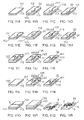
- Fig. 1 schematically illustrates an apparatus 1 according to an example of the disclosure.
- the apparatus 1 illustrated in Fig. 1 comprises a deformable substrate 3, at least one support 5 and a curved support structure 7. Only features relevant to the following description have been illustrated in Fig.1 . It is to be appreciated that in other examples other features may be included.
- the apparatus 1 may be configured to be incorporated within an electronic device such as a sensor device a medical or biological sensing device, a wearable electronic device, a mobile cellular telephone or any other suitable electronic device.
- the deformable substrate 3 comprises a planar surface 9.
- the planar surface 9 is flat or substantially flat.
- the deformable substrate 3 may have a different shape. For example it may be curved and/or the surface 9 of the deformable substrate 3 need not be flat.
- the equilibrium shape of the deformable substrate 3 may be the flat configuration illustrated in Fig.1 .
- the equilibrium shape is the position and shape which the deformable substrate 3 will adopt when no external force is applied by the user of the apparatus 1.
- the deformable substrate 3 may have a different equilibrium shape, for example, the equilibrium shape may comprise at least a part of the deformable substrate 3 being bent or curved.
- the deformable substrate 3 may comprise both flat and curved portions.
- the deformable substrate 3 may comprise at least one user-deformable portion which may be configured to change shape in response to a physical force applied by a user of the apparatus 1.
- the change in shape may comprise bending, folding, twisting, stretching, compression, shearing or any other suitable deformation of a portion of the deformable substrate 3.
- the deformable substrate 3 may be configured to automatically return to the equilibrium shape when the force applied by the user is removed.
- the deformable substrate 3 may be configured to be stretched in the directions indicated by the arrows 10, 12.
- the arrow 10 indicates the principal direction of stretch. In this example the principal direction of stretch is parallel or substantially parallel to the at least one support 5.
- the arrow 12 indicates a secondary direction of stretch. In this example the secondary stretch is perpendicular or substantially perpendicular to the at least one support 5.
- the deformable substrate 3 may comprise a flexible substrate which may be bent or twisted by a user.
- the deformable substrate 3 may comprise a polymer material, elastomeric material or any other material which may be deformed in response to a force applied by the user of the apparatus 1.
- the deformable substrate 3 may comprise a plurality of hinged or jointed segments.
- the hinged or jointed segments may be configured to be moved with respect to each other to enable a portion of the deformable substrate 3 to be folded or bent or stretched.
- the deformable substrate 3 may be folded or bent or stretched in response to a force applied by the user of the apparatus 1.
- one or more electronic components may be mounted on the deformable substrate 3.
- the apparatus 1 illustrated in Fig. 1 also comprises at least one support 5.
- the at least one support 5 may comprise any means which may be configured to support one or more curved support structures 7 in a position spaced from the deformable substrate 3.
- the at least one support 5 comprises a beam 6 which extends in a direction perpendicular to the planar surface 9 of the deformable substrate 3.
- the at least one support 5 comprises a beam 6 which extends along a portion of the planar surface 9 of the deformable substrate 3. It is to be appreciated that other types of support may be used in other example apparatus 1.
- the at least one support 5 may comprise a plurality of individual supports which are located separated from each other on the surface 9 of the deformable substrate 3.
- the plurality of individual supports may be any suitable size or shape for example, the individual supports may be square or rectangular or cylindrical or any other suitable shape. In some examples different individual supports may have different sizes and/or shapes.
- the at least one support 5 may be configured to be deformable in response to a force applied by a user.
- the at least one support 5 may be configured to bend or stretch or be compressed or any other suitable deformation in response to a force applied by a user.
- the at least one support 5 may be configured so that it is not deformable in response to a force applied by a user.
- the at least one support 5 may comprise a rigid material so that the at least one support 5 is not compressed when a force is applied by a user.
- the at least one support 5 may be coupled to the deformable substrate 3 so that if the deformable substrate 3 is deformed this also causes movement of the at least one support 5 from its equilibrium position.
- the support 5 comprises a beam 6 which is mounted on the deformable substrate 3 so that it extends along a portion of the planar surface 9 of the deformable substrate 3. If the portion of the deformable substrate 3 on which the beam 6 is mounted is deformed then the beam 6 is also deformed.
- the deformable substrate 3 may be deformed by being stretched, twisted or bent for example so the beam 6 may also be stretched, twisted or bent.
- the beam 6 may comprise a flexible material such as polymeric material, elastomeric material or any other material which may be deformed in response to a force applied by the user of the apparatus 1 but which is rigid enough to support the curved support structure 7.
- the at least one support 5 may comprise a plurality of individual supports which are located separated from each other on the surface 9 of the deformable substrate 3 rather than a continuous beam. In such examples deforming a portion of the deformable substrate 3 will cause changing the positions or relative orientations of the respective supports 5 and need not cause a deformation of an individual support.
- the supports 5 may be made of any suitable material which may be configured to support the curved support structure 7.
- the apparatus 1 illustrated in Fig. 1 also comprises a curved support structure 7.
- the curved support structure 7 may be configured to support at least a portion of a resistive sensor 30 wherein the resistive sensor 30 comprises a first electrode 31, a second electrode 33 and a resistive sensor material 35 provided between the electrodes 31, 33. Examples of resistive sensors 30 which may be supported by the curved support structure 7 are described below with reference to Figs. 3A to 9B .
- the curved support structure 7 may comprise any suitable material.
- the curved support structure 7 may comprise a non-conductive material.
- the curved support structure 7 may comprise a polymer or other suitable material.
- the resistive sensor material 35 and the electrodes 31, 33 of the resistive sensor 30 may be mounted on the curved support structure 7.
- the curved support structure 7 may comprise a conductive material.
- the curved support structure 7 may comprise copper or other suitable material.
- the curved support structure may provide the first electrode 31.
- the resistive sensor material 35 and the second electrode 33 may be supported by the first electrode 31.
- the curved support structure 7 may be coupled to the deformable substrate 3 via the at least one support 5.
- the at least one support 5 is configured to separate the curved support structure 7 from the substrate so that the curved support structure 7 is, at least partially, isolated from the deformable substrate 3.
- the at least one support 5 is positioned between the curved support structure 7 and the deformable substrate 3.
- the at least one support 5 may maintain the curved support structure 7 in a position which is spaced from the deformable substrate 3 so that the curved support structure 7 and the deformable substrate 3 are separated from each other.
- the distance of the separation between the curved support structure 7 and the deformable substrate 3 may be dependent on the height of the at least one support 5. In the example of Fig. 1 the distance of the separation between the curved support structure 7 and the deformable substrate 3 is the same as the height of the beam 6.
- the curved support structure 7 and the at least one support 5 may be configured so that the curved support structure 7 does not directly contact the deformable substrate 3. In some examples the curved support structure 7 and the at least one support 5 may be configured so that the curved support structure 7 does not directly contact the deformable substrate 3 when the apparatus 1 is in an equilibrium, non-deformed state. In some examples the curved support structure 7 and the at least one support 5 may be configured so that the curved support structure 7 does not directly contact the deformable substrate 3 when the apparatus 1 is in a deformed state.
- the curved support structure 7 comprises an elongate member 11 which is coupled to the at least one support 5 at a plurality of different points along the length of the elongate member 11.
- the elongate member 11 is curved.
- the elongate member 11 may comprise a plurality of curves.
- the total length of the elongate member 11 is greater than the length of the deformable substrate 3 over which the elongate member 11 extends.
- the curved portion 16 of the elongate member 11 has an angle of curvature greater than 180 degrees so that the elongate member 11 doubles back on itself to form a loop 13.
- the loop 13 comprises an opening 14 so the loop 13 is not closed.
- the elongate member 11 comprises a plurality of loops 13.
- the plurality of loops 13 form a serpentine shape in which a loop 13 which extends to the left hand side of the beam 6 is followed by a loop 13 which extends to the right hand side of the beam 6.
- the elongate member 11 is configured so that the curved support structure 7 is distributed on either side of the beam 6.
- the curved support structure 7 may be coupled to the at least one support 5 at a plurality of different points along the length of the elongate member 11. In the example of Fig. 1 the curved support structure 7 is coupled to the beam 6 at two points in each loop 13.
- curved support structure 7 illustrated in Fig. 1 is an example and other shapes could be used in other examples.
- the apparatus 1 may comprise a plurality of curved support structures 7.
- the curved support structures 7 may extend in the same direction along the deformable substrate 3.
- additional curved structures may be provided overlaying the curved support structures 7.
- the additional curved structures may extend in a direction perpendicular or substantially perpendicular to the curved support structure 7. Examples of apparatus 1 comprising curved support structures 7 and additional curved structures are described below with reference to Figs. 7A to 9B .
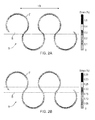
- Figs. 2A and 2B show the first principal strain on the surface of two example curved support structures 7.
- Fig. 2A shows the first principal strain for a polymer curved support structure 7
- Fig. 2B shows the first principal strain for a metal curved support structure 7.
- copper was used as the metal.
- a strain of 20% was applied to the apparatus 1.
- the maximum strain observed in the curved support structure 7 is observed at the edges of the curved support structure 7.
- the maximum strain observed is only +/-0.5% which is two orders of magnitude smaller than the strain which is applied to the apparatus 1. It can be seen from Figs. 2A and 2B that very little strain is present in the curved support structures 7 even when a large strain is applied to the apparatus 1. Close to the centre of the conductive support structure 7 the strain is zero or very close to zero.
- the curved support structure 7 is configured to support at least a portion of a resistive sensor 30 so that the resistive sensor 30 is subjected to a reduced strain when the apparatus 1 is deformed.
- Figs. 3A and 3B schematically illustrate resistive sensors 30 which may be used in examples of the disclosure.
- the resistive sensor 30 comprises a first electrode 31 and second electrode 33 and resistive sensor material 35.
- the resistive sensor material 35 forms an electrical connection between the electrodes 31, 33.
- the resistive sensor material 35 may provide a direct current path between the two electrodes 31, 33.
- the electrodes 31 and 33 may comprise any conductive material.
- the electrodes 31, 33 may comprise copper, silver, gold, graphene, indium tin oxide (ITO) or any other suitable material.
- the resistive sensor material 35 may comprise a material which has a variable resistance.
- the resistive sensor material 35 may have a resistance which varies in dependence on the presence of a parameter which is sensed by the resistive sensor material 35.
- the sensed parameter may comprise an environmental parameter such as a chemical which may be present in the environment around the resistive sensor 30 or any other physical parameter which may be detected such as temperature or light.
- the resistive sensor material 35 may have a resistive transduction mechanism so that the resistivity of the resistive sensor material 35 changes in response to the parameter to be sensed.
- the material which is used as the resistive sensor material 35 may be determined by the parameter which is to be sensed.
- the resistive sensor material 35 may be used to enable the resistive sensor 30 to detect humidity.
- the resistive sensor material 35 may comprise a material such as graphene oxide.
- the resistive sensor material 35 may be configured to detect changes in temperature.
- Examples of the resistive sensor material 35 which may be used in such examples include Silicon Carbide or any other suitable material.
- the resistive sensor material 35 may comprise a photoresitive material which may enable the resistive sensor 30 to be used to detect the ambient light.
- Fig. 3A schematically illustrates an example arrangement resistive sensor 30 which may be used in examples of the disclosure where the resistive sensor material 35 has a high sheet resistance.
- the distance d between the electrodes 31, 33 may be small and the length of the electrodes 31, 33 / may be large. This gives a low separation to length ( d / l ratio for the resistive sensor 30.
- the example resistive sensor 30 arrangement of Fig. 3A may be used with a resistive sensor material 35 such as graphene oxide which has a sheet resistance of around 5G ⁇ /sq at 50nm when the graphene oxide is 50nm thick.
- Fig. 3B schematically illustrates an example arrangement resistive sensor 30 which may be used in examples of the disclosure where the resistive sensor material 35 has a low sheet resistance.
- the distance d between the electrodes 31, 33 may be large and the length of the electrodes 31, 33 / may be small. This gives a high separation to length d / l ratio for the sensor 30.
- the example resistive sensor 30 arrangement of Fig. 3A may be used with a resistive sensor material 35 such as a thermistor paste which may have a sheet resistance of 5 ⁇ /sq.
- Figs. 4A to 9B show example apparatus 1 in which a resistive sensor 30 is supported by a curved support structure 7.
- Figs. 4A and 4B illustrate an example apparatus 1 according to an example of the disclosure.
- Fig. 4A illustrates a plan view of an apparatus 1
- Fig 4B illustrates a cross section through a portion of the apparatus 1.
- the example apparatus 1 comprises a curved support structure 7 and at least one support 5 which may be as described above in relation to Fig. 1 .
- the curved support structure 7 supports a resistive sensor 30.
- the curved support structure 7 comprises a non-conductive material.
- the curved support structure 7 comprises a polymer material. In other examples other materials may be used.
- the curved support structure 7 supports the first electrode 31, the second electrode 33 and the resistive sensor material 35 of the resistive sensor 30.
- the first electrode 31 is provide on a first edge 41 of the curved support structure 7 and a second electrode 33 is provided on a second edge 43 of the curved support structure 7.
- the resistive sensor material 35 is provided between the two electrodes 31, 33.
- the resistive sensor material 35 provides an electrical connection between the two electrodes 31, 33.
- the resistive sensor material 35 is provided in the centre portions of the curved support structure 7. This may be the region of the curved support structure 7 which undergoes the least strain. This may minimise the strain within the resistive sensor material 35 when the apparatus 1 is deformed.
- the electrodes 31, 33 extend along the length of the curved support structure 7.
- the electrodes 31, 33 are arranged to have low separation to length d / l ratio.
- the example resistive sensor 30 arrangement of Figs. 4A and 4B may be used with a resistive sensor material 35 which has a high sheet resistance.
- Figs. 5A to 5C illustrate an example apparatus 1 according to another example of the disclosure.
- Fig. 5A illustrates a plan view of an apparatus 1.
- Fig 5B illustrates a cross section through a portion of the apparatus 1 in which the curved support structure 7 comprises a conductive material.
- Fig 5C illustrates a cross section through a portion of the apparatus 1 in an alternative example in which the curved support structure 7 comprises a non-conductive material.
- the example apparatus 1 comprises a curved support structure 7 and at least one support 5 which may be as described above in relation to Fig. 1 .
- the curved support structure 7 supports at least a portion of a resistive sensor 30.
- the curved support structure 7 comprises a conductive material.
- the curved support structure 7 provides the first electrode 31.
- the curved support structure 7 may comprise any suitable material such as copper or other conductive material.
- the first electrode 31 supports the resistive sensor material 35 and the second electrode 33.
- the resistive sensor material 35 and the second electrode 33 may be deposited directly on the first electrode 31.
- the resistive sensor material 35 may be provided as a layer overlaying the first electrode 31.
- the second electrode 33 may be provided in a layer overlaying resistive sensor material 35.
- the resistive sensor material 35 may be provided between the first electrode 31 and the second electrode 33 to provide an electrical connection between the two electrodes 31, 33.
- the material and thickness of the material which is used as the first electrode 31 is selected to enable the weight of the resistive sensor material 35 and the second electrode 33 to be supported by the first electrode 31.
- the cross section of Fig. 5C shows an alternative arrangement for a resistive sensor 30.
- the curved support structure 7 comprises a non-conductive material such as a polymer material. In other examples other materials may be used.
- the curved support structure 7 supports the first electrode 31, the second electrode 33 and the resistive sensor material 35.
- the first electrode 31 is provided as a first layer on the curved support structure 7.
- the resistive sensor material 35 is provided as a layer overlaying the first electrode 31.
- the second electrode 33 is provided in a layer overlaying the resistive sensor material 35.
- the resistive sensor material 35 provides an electrical connection between the two electrodes 31, 33.
- the resistive sensor material 35 is deposited across the width of the curved support structure 7.
- the resistive sensor material 35 may cover the centre portion of the curved support structure 7 and the edges of the curved support structure 7.
- the strain which is present in the curved support structure 7 when the apparatus 1 is deformed may be low enough so that it does not affect the resistive sensor material 35.
- the second electrode 33 is provided as three strips 51 overlaying the resistive sensor material 35.
- the strips 51 do not completely cover the resistive sensor material 35. This enables the resistive sensor 30 to be permeable to the parameter which is to be sensed by the resistive sensor material 35. It is to be appreciated that in other examples other arrangements may be used to provide gaps in the second electrode 33.
- the second electrode 33 may be continuous with no gaps. In such examples the second electrode 33 may be arranged to be permeable to the parameter which is to be sensed by the resistive sensor material 35.
- an optically transparent material such as indium tin oxide (ITO) may be provided overlaying a resistive sensor material 35 which is configured to detect incident light.
- the electrodes 31, 33 extend along the length of the curved support structure 7 so that the electrodes 31, 33 have low separation to length d / l ratio.
- the example resistive sensor 30 arrangement of Figs. 5A to 5C may be used with a resistive sensor material 35 which has a high sheet resistance.
- the example resistive sensor 30 of Figs. 4A to 5C may be used with a resistive sensor material 35 such as graphene oxide which may be configured to detect humidity.
- a resistive sensor material 35 such as graphene oxide which may be configured to detect humidity.
- Such resistive sensors 30 may be used to provide a stretchable humidity sensor device.
- the device could be worn as a patch on the body of a user and may be used to measure levels or perspiration or other biological parameters.
- Fig. 6 illustrates a cross section of an example apparatus 1.
- the apparatus 1 comprises a deformable substrate 3, at least one support 5 and a curved support structure 7 which may be as described in relation to Fig. 1 .
- the cross section may be taken perpendicular to the principal direction of strain in Fig. 1 .
- the curved support structure 7 may support a resistive sensor 30 or a plurality of resistive sensors 30.
- the deformable substrate 3 comprises a lower portion 61 and an upper portion 63.
- the deformable substrate 3 forms a cavity 69 in which the curved support structure 7 and the resistive sensor 30 or plurality of resistive sensors 30 are provided.
- additional support pillars 65 are provided between the upper portion 63 of the deformable substrate 3 and the lower portion 61 of the deformable substrate 3.
- the additional support pillars 65 may be formed from the same material as the deformable substrate 3.
- the additional support pillars 65 may be configured to prevent the upper portion 63 of the deformable substrate 3 from coming into contact with the curved support portion 7 when the apparatus 1 is deformed.
- the upper portion 63 of the deformable substrate 3 comprises one or more vent holes 67.
- the vent holes 67 may be configured to enable the environmental parameters which are to be detected to pass through the upper portion 63 of the deformable substrate 3 and reach the resistive sensor 30.
- the vent holes 67 may comprise gaps or discontinuities in the upper portion 63 of the deformable substrate 3.
- the vent holes 67 may comprise portions of the upper portion 63 of the deformable substrate 3 which are permeable to an environmental parameter which is to be detected.
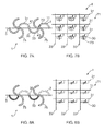
- Figs. 7A and 7B illustrate an example of an apparatus 1 comprising an array 71 of resistive sensors 30.
- the array 71 of resistive sensors 30 may comprise a plurality of resistive sensors 30.
- different resistive sensors 30 within the array 71 may be configured to sense different parameters.
- different resistive sensor materials 35 may be used in different resistive sensors 30.
- Fig. 7A illustrates a plan of a section of the apparatus 1.
- Fig. 7B provides an equivalent circuit diagram for a three by three array 71 of resistive sensors 30. It is to be appreciated that the array 71 of resistive sensors 30 may comprise any suitable number of resistive sensors 30 in any suitable arrangement.
- the apparatus 1 of Figs. 7A and 7B comprise a deformable substrate 3, at least one support 5 and a curved support structure 7 which may be as described in relation to Fig. 1 . Only one curved support structure 7 is illustrated in Fig. 7A however it is to be appreciated that the apparatus 1 may comprise a plurality of curved support structures 7. The plurality of curved support structures 7 may extend in the same direction.
- the apparatus 1 also comprises a plurality of additional curved structures 75.
- the additional curved structures 75 may comprise an elongate member 11.
- the elongate member 11 may form a serpentine shape.
- the serpentine shape may be the same or similar to the serpentine shape of the curved support structure 7.
- the additional curved structures 75 extend in a direction perpendicular to the curved support structures 7.
- the additional curved structures 75 are provided spaced along the length of the curved support structures 7 so that there are a plurality of intersecting points where an additional curved structure 75 crosses over a curved support structure 7.
- the additional curved structures 75 are provided overlaying the curved support structures 7.
- the additional curved structures 75 may comprise an electrical connection to the second electrode 33.
- the additional curved structures 75 provide cross connectors for the array 71 of resistive sensors 30.
- the example apparatus 1 of Figs. 7A and 7B uses a resistive sensor 30 arrangement as illustrated in Figs. 4A and 4B and described above.
- the electrodes 31, 33 are provided on the edges 41, 43 of the curved support structure 7 and the resistive sensor material 35 is provided between the electrodes 31, 33.
- the resistive sensors 30 are provided in sections along the length of the curved support structure 7.
- the length of the sections of resistive sensors 30 can be selected to control the sensitivity of the resistive sensors 30.
- the length of the discontinuous electrode 33 and/or the thickness of the resistive sensor material 35 may be adjusted to tune the resistance of the resistive sensor 30.
- a dielectric insulating material 73 is provided between the first electrode 31 and the additional support structure 75.
- the dielectric insulating material 73 may be configured to prevent a direct connection between the first electrode 31 and the cross connector.
- Figs. 8A and 8B illustrate another example of an apparatus 1 comprising an array 71 of resistive sensors 30.
- the array 71 of resistive sensors 30 may comprise a plurality of resistive sensors 30.
- Different resistive sensors 30 within the array 71 may be configured to sense different parameters.
- different resistive sensor materials 35 may be used in different resistive sensors 30.
- Fig. 8A illustrates a plan of a section of the apparatus.
- Fig. 8B provides an equivalent circuit diagram for a three by three array 71 of resistive sensors 30. It is to be appreciated that the array 71 of resistive sensors 30 may comprise any suitable number of resistive sensors 30 in any suitable arrangement.
- the apparatus 1 of Figs. 8A and 8B comprise a deformable substrate 3, at least one support 5 and a curved support structure 7 which may be as described in relation to Fig. 1 . Only one curved support structure 7 is illustrated in Fig. 8A however it is to be appreciated that the apparatus 1 may comprise a plurality of curved support structures 7. The plurality of curved support structures 7 may extend in the same direction.
- the apparatus 1 also comprises a plurality of additional curved structure 75.
- the additional curved structures may comprise an elongate member 11.
- the elongate member 11 may form a serpentine shape.
- the serpentine shape may be the same or similar to the serpentine shape of the curved support structure 7.
- the additional curved structures 75 extend in a direction perpendicular to the curved support structures 7.
- the additional curved structures 75 are provided spaced along the length of the curved support structures 7 so that there are a plurality of intersecting points where an additional curved structure 75 crosses over a curved support structure 7.
- the additional curved structures 75 are provided overlaying the curved support structures 7.
- the additional curved structures 75 may comprise an electrical connection to the second electrode 33.
- the additional curved structures 75 provide cross connectors for the array 71 of resistive sensors 30.
- the example apparatus 1 of Figs. 8A and 8B uses a resistive sensor 30 arrangement as illustrated in Figs. 5A to 5C and described above.
- the first electrode 31 is provided underneath the resistive sensor material 35 and so is not illustrated in the plan view of Fig. 8A .
- the resistive sensors 30 are provided in sections along the length of the curved support structure 7.
- the length of the sections of resistive sensors 30 and the width of the discontinuous electrode 33 and/or the thickness of the resistive sensor material 35 may be adjusted to tune the resistance of the resistive sensor 30.
- each of the resistive sensors 30 within the array 71 may be read independently by multiplexing read electronics.
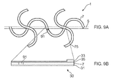
- Figs. 9A and 9B illustrate an example apparatus 1 according to another example of the disclosure.
- the example apparatus 1 of Figs. 9A and 9B may be suitable for a user with a resistive sensor material 35 with a low sheet resistance.
- Fig. 9A illustrates a plan view of an apparatus 1
- Fig. 9B illustrates a cross section through a portion of the apparatus 1.
- the example apparatus 1 comprises a curved support structure 7 and at least one support 5 which may be as described above in relation to Fig. 1 . Only one curved support structure 7 is illustrated in Fig. 9A however it is to be appreciated that the apparatus 1 may comprise a plurality of curved support structures 7.
- the example apparatus 1 of Figs. 9A and 9B also comprise a plurality of additional curved structure 75.
- Two additional curved structures 75 are illustrated in Fig. 9A however it is to be appreciated that any number may be provided within the apparatus 1.
- the additional curved structures 75 comprise an elongate member 11 in a serpentine shape.
- the serpentine shape of the additional curved structure 75 may be the same or similar to the serpentine shape of the curved support structure 7.
- the additional curved structures 75 extend in a direction perpendicular to the curved support structures 7.
- the additional curved structures 75 are provided spaced along the length of the curved support structures 7 so that there are a plurality of intersecting points where an additional curved structure 75 crosses over a curved support structure 7.
- the additional curved structures 75 are provided overlaying the curved support structures 7.
- the additional curved structure 75 may provide second electrode 33 for one or more resistive sensors 30.
- the curved support structure 7 comprises a non-conductive material.
- the curved support structure 7 comprises a polymer material. In other examples other materials may be used.
- the first electrode 31 is provided as a layer underneath the curved support structure 7.
- the first electrode 31 may extend along the length of the curved support structure 7.
- the first electrode 31 may extend continuously along the length of the curved support structure 7.
- the resistive sensor material 35 is provided as a layer overlaying the curved support structure 7.
- the resistive sensor material 35 may extend along the length of the curved support structure 7.
- the resistive sensor material 35 may be provided covering the whole width of the curved support structure 7.
- the resistive sensor material 35 may only be provided on the portions of the curved support structure 7 which are subjected to the lowest amount of strain when the apparatus 1 is deformed.
- the resistive sensor material 35 might only be provided in the central portion of the curved support structure 7. This may enable materials which are very sensitive to strain to be used as the resistive sensor material 35.
- the second electrode 33 is provided by the additional support structure 75.
- a via 91 is provided through the curved support structure 7 to enable the resistive sensor material 35 to electrically connect the first and second electrodes 31, 33.
- the via 91 may be provided at points along the curved support structure 7 which are subjected to the lowest amount of strain when the apparatus 1 is deformed.
- the first electrode 31 is provided on the curved support structure 7 while the second, cross connector electrode 33 is provided on an additional support structure 75 and the resistive sensor material 35 extends along the length of the support structure 7.
- the resistance is measured between the position of the via 91 and the cross connector electrode 33.
- This arrangement gives the resistive sensor 30 a high separation to length d / l ratio.
- the example resistive sensor 30 arrangement of Figs. 9A and 9B may be used with a resistive sensor material 35 which has a low sheet resistance.
- the apparatus of Figs. 9A and 9B may be used with a material such as Silicon Carbide which may be used to detect changes in temperature.
- a plurality of sensors 30 as illustrated in Figs. 9A and 9B may be provided in an array 71.
- the equivalent circuit diagram may be the same as Fig. 8B .
- Each of the resistive sensors 30 within the array 71 may be read independently by multiplexing read electronics.
- Figs. 10 to 13 illustrate example methods which may be used to provide apparatus 1 according to examples of the disclosure.
- the apparatus 1 may be as described above with regards to Figs. 1 to 9B .
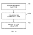
- Fig. 10 illustrates a first example method.
- the method comprises, at block 101, providing a deformable substrate 3.
- the method comprises, at block 103, providing a curved support structure 7.
- the curved support structure 7 is configured to support at least a portion of a resistive sensor 30 wherein the resistive sensor 30 comprises a first electrode 31, a second electrode 33 and a resistive sensor material 35 provided between the electrodes 31, 33.
- the method also comprises, at block 105, providing at least one support 5 configured to space the curved support structure 7 from the deformable substrate 3 so that when the deformable substrate 3 is deformed the curved support structure 7 is not deformed in the same way.
- the resistive sensor 30 is positioned on the curved support structure 7 so as to limit deformation of the resistive sensor 30 when the deformable substrate 3 is deformed.
- Figs. 11A to 11R also illustrate an example method of providing an apparatus 1.
- the example method of Figs. 11A to 11R may be used to provide an apparatus 1 such as the apparatus 1 of Figs. 4A and 4B and 7A and 7B .
- a release layer 111 is deposited on a silicon wafer 113.
- a photoresist layer 115 is deposited on the release layer 111.
- the photoresist layer 115 is patterned as an electrode 33.
- a conductive material 117 such as metal, is deposited on the photoresist layer 115.
- the conductive material 117 may be deposited using any suitable means such as evaporation or sputtering.
- the photoresist layer 115 is removed and the electrode 33 is left on the release layer 111.
- the electrode 33 which is formed may provide the second electrode 33 as illustrated in Figs. 7A and 7B .
- This electrode 33 may comprise part of an additional curved structure 75 and extend along a portion of a curved support structure 7.
- dielectric insulating material 73 is deposited on the electrode 33.
- the dielectric insulating material 73 may be deposited using any suitable means such as inkjet printing or screen printing.
- another photoresist layer 119 is deposited on the release layer 111.
- the photoresist layer 119 is patterned as another electrode 31.
- a conductive material 121 such as metal, is deposited on the photoresist layer 119.
- the conductive material 121 may be deposited using any suitable means such as evaporation or sputtering.
- Fig. 11H the photoresist layer 119 is removed and the two electrodes 31, 33 are left on the release layer 111.
- the electrode 31 which is formed in the blocks of the method of Figs. 11F to 11 H may form the first electrode 31 as illustrated in Figs. 7A and 7B .
- This electrode 31 may be arranged to extend along a portion of a curved support structure 7.
- Fig. 11I another photoresist layer 123 is deposited on the release layer 111.
- the photoresist layer 123 is patterned as the resistive sensor material 35.
- a resistive sensor material 35 is deposited on the photoresist layer 123.
- the resistive sensor material 35 may be any material which has a resistance which varies in response to a sensed parameter.
- the resistive sensor material 35 may be deposited using any suitable means such as evaporation, sputtering, screen printing or any other suitable means.
- the method used may to deposit the resistive sensor material 35 may depend on the material which is used. As an example, graphene oxide could be bar coated or spray coated from a solution.
- Fig. 11K the photoresist layer 123 is removed and the resistive sensor material 35 is left between the two electrodes 31, 33.
- a polymer 125 is deposited onto the electrodes 31, 33.
- the polymer 125 may be a photopatternable polymer.
- the polymer 125 may be spin coated onto the electrodes 31, 33. In other examples other means for depositing the polymer 125 may be used.
- another photoresist layer 127 is deposited on the polymer 125.
- the photoresist layer 127 is patterned as the curved support structure 7 and the additional curved structure 75.
- the polymer 125 is then exposed to ultra-violet (UV) light 129.
- UV light 129 hardens the polymer 125 which is exposed to the UV light by increasing the number of crosslinks in the polymer 125.
- a further photoresist layer 131 is deposited.
- the further photoresist layer 131 is patterned as the at least one support 5.
- the at least one support 5 comprises a beam 6.
- an elastomer layer 133 is cast against the further photoresist layer 131 and cured.
- the further photoresist layer 131 and the lift off layer 111 are removed leaving a deformable substrate 3, beam 6 and curved support structure 7.
- Fig. 11R the structure is inverted to leave an apparatus 1 as described above and illustrated in Figs. 7A and 7B .
- Figs. 11A to 11R could be modified to provide different examples apparatus 1.
- the method could be modified to provide an example apparatus 1 with stacked electrodes 31, 33 as in Figs. 8A and 8B .
- the block of Fig. 11E could be removed as no dielectric insulating material 73 is needed.
- the blocks of Figs. 11I to 11 K could be switched with the blocks of Figs. 11F to 11 H so that the resistive sensor material 35 is provided as a layer between the two electrodes 31, 33.
- the shapes of the electrodes 31, 33 and the resistive sensor material 35 could be adjusted accordingly.
- the method could also be modified to provide an example apparatus 1 which may use a resistive sensor material 35 with a low sheet resistance.
- the method could be modified to provide an apparatus 1 such as the apparatus of Figs. 9A and 9B .
- the block of Fig. 11E could be removed as no dielectric insulating material 73 is needed.
- the blocks of Figs. 11F to 11 H could be switched with the blocks of Figs. 11I to 11 N so that the curved support structure 7 is provided between the electrodes 31, 33.
- the mask used to produce the curved support structure 7 may be modified to enable the vias 91 to be added.
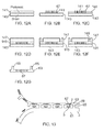
- Figs. 12A to 12G show a method for producing part of an apparatus 1 such as the apparatus 1 illustrated in Fig. 6 .
- a photoresist layer 141 is deposited onto a silicon substrate 143.
- the photoresist layer 141 may be spin coated onto the silicon substrate 143.
- Other means of depositing a photoresist layer 141 may be used in other examples of the disclosure.
- Fig. 12B the layer of photoresist 141 is patterned as vent holes 67.
- the vent holes 67 may be arranged in any suitable pattern.
- Fig. 12C an elastomer layer 145 is cast against the photoresist layer 141 and cured. This elastomer layer 145 may form part of an upper portion 63 of a deformable substrate 3.
- a second photoresist layer 147 is deposited over the elastomer layer 145.
- the second photoresist layer 147 may be spin coated onto the elastomer layer 145 or any other suitable means may be used.
- the photoresist layer 147 is patterned as additional support pillars 65.
- another elastomer layer 149 is cast against the second photoresist layer 147 and cured. This elastomer layer 149 may form the additional support pillars 65 as described above with reference to Fig. 6 .
- Fig. 12G the second photoresist layer 147 is removed leaving an upper portion 63 of a deformable substrate 3 with vents 67 and additional support pillars 65.
- Fig. 13 illustrates an example method which may be used to combine the upper portion 63 of a deformable substrate 3 with the lower portion 61 of the deformable substrate 3.
- the upper portion 63 of the deformable substrate 3 may be formed as described with relation to Figs. 12A to 12G .
- the lower portion 61 of the deformable substrate 3 may be formed as described with relation to Figs. 11A to 11R .
- the lower portion 61 of the deformable substrate 3 may comprise a curved support structure 7 and resistive sensors 30.
- the upper portion 63 and the lower portion 61 are bonded in a roll-to-roll process after brief plasma treatment to promote bonding.
- Examples of the disclosure provide an apparatus 1 which can be used for sensing. As the resistive sensors 30 within the apparatus 1 are not affected by the deformation of the apparatus 1 this makes the apparatus 1 suitable for use in bendable or deformable electronic devices. For example the apparatus 1 may be used in wearable electronic devices.
- the curved support structure 7 is coupled to the deformable substrate 3 via the at least one support 5 which enables the curved support structure 7 to be positioned spaced from the deformable substrate 3.
- a user applies a force to the deformable substrate 3 this may cause a change in size or shape of the deformable substrate 3.
- the curved support structure 7 is not directly coupled to the deformable substrate 3 the forces applied to the deformable substrate are not also applied to the curved support structure 7. This means that the conductive portion does not bend or change size or shape in the same way that the deformable substrate does. This may reduce the amount of stress within the curved support structure 7 and reduce the likelihood of failure due to fatigue.
- the resistive sensors 30 are provided on the curved support structure 7 and not as additional rigid portions. This means that the resistive sensors 30 do not add any rigid portions to the apparatus and do not reduce the flexibility of the apparatus 1.
- the resistive sensors 30 may be arranged so that an array 71 of resistive sensors can be read by commercially available electronics.
- the array 71 of resistive sensors 30 may comprise any number of resistive sensors 30. This may enable information to be obtained from a large number of resistive sensors 30.
- example or “for example” or “may” in the text denotes, whether explicitly stated or not, that such features or functions are present in at least the described example, whether described as an example or not, and that they can be, but are not necessarily, present in some of or all other examples.
- example “for example” or “may” refers to a particular instance in a class of examples.
- a property of the instance can be a property of only that instance or a property of the class or a property of a sub-class of the class that includes some but not all of the instances in the class. It is therefore implicitly disclosed that a features described with reference to one example but not with reference to another example, can where possible be used in that other example but does not necessarily have to be used in that other example.
Landscapes
- Engineering & Computer Science (AREA)
- Microelectronics & Electronic Packaging (AREA)
- Computer Hardware Design (AREA)
- Measurement Of Length, Angles, Or The Like Using Electric Or Magnetic Means (AREA)
- Force Measurement Appropriate To Specific Purposes (AREA)
- User Interface Of Digital Computer (AREA)
- Testing Or Calibration Of Command Recording Devices (AREA)
- Transmission And Conversion Of Sensor Element Output (AREA)
- Investigating Or Analyzing Materials By The Use Of Electric Means (AREA)
Abstract
An apparatus and method wherein the method comprises: a deformable substrate; a curved support structure configured to support at least a portion of a resistive sensor wherein the resistive sensor comprises a first electrode, a second electrode and a resistive sensor material provided between the electrodes; at least one support configured to space the curved support structure from the deformable substrate so that when the deformable substrate is deformed the curved support structure is not deformed in the same way; wherein the resistive sensor is positioned on the curved support structure so as to limit deformation of the resistive sensor when the deformable substrate is deformed.
Description
- Examples of the present disclosure relate to a deformable apparatus and method. In particular, they relate to a deformable apparatus and method wherein the apparatus is configured for sensing.
- Materials with resistive characteristics configured to respond to a change in one or more physical parameters are known. Such materials can be incorporated into sensors to enable the physical parameter or a change in the physical parameter to be detected. Physical parameters which can be detected using such materials comprise temperature, humidity, strain, chemical and biological parameters or any other suitable parameter.
- It is useful to be able to incorporate these sensors into a deformable apparatus such as a stretchable and/or bendable electronic device. When such sensors are incorporated into a deformable apparatus it is necessary to ensure that the sensors can perform reliably during stretching or other deformation of the apparatus. It is also useful to incorporate the sensors into the apparatus without affecting the ability of the deformable apparatus to be stretched or otherwise deformed repeatedly.
- According to various, but not necessarily all, examples of the disclosure, there may be provided an apparatus comprising: a deformable substrate; a curved support structure configured to support at least a portion of a resistive sensor wherein the resistive sensor comprises a first electrode, a second electrode and a resistive sensor material provided between the electrodes; at least one support configured to space the curved support structure from the deformable substrate so that when the deformable substrate is deformed the curved support structure is not deformed in the same way; wherein the resistive sensor is positioned on the curved support structure so as to limit deformation of the resistive sensor when the deformable substrate is deformed.
- In some examples the electrodes may extend along a length of the curved support structure.
- In some examples a plurality of resistive sensors may be provided on the curved support structure.
- In some examples a plurality of curved support structures may be provided.
- In some examples a first plurality of curved support structures may be provided extending in a first direction and a second plurality of curved structures are provided overlaying the first plurality of curved support structures and extending in a second direction where the second direction is perpendicular to the first direction. The second electrode may be provided on a second curved structure. The first curved support structure may comprise a polymer layer provided between the first electrode and the second electrode. A via may be provided through the polymer layer to connect the first electrode and the second electrode.
- In some examples the first curved support structure may comprise the first electrode such that the resistive sensor material and the second electrode are supported by the first electrode.
- In some examples the first curved support structure may comprise a polymer layer and the first and second electrodes and the resistive sensor material are supported by the polymer layer.
- In some examples the deformable substrate may form a cavity in which the curved support structure and resistive sensor are provided.
- In some examples a radius of curvature of the curved support structure may be parallel to a plane of the deformable substrate.
- In some examples the curved support structure may have a serpentine shape. The serpentine shape may comprise a plurality of loops such that a loop which extends to a left hand side is followed by a loop which extends to a right hand side.
- In some examples the deformable substrate may be configured to be deformed in response to a force applied by a user.
- According to various, but not necessarily all, examples of the disclosure, there may be provided an electronic device comprising an apparatus as described above.
- According to various, but not necessarily all, examples of the disclosure, there may be provided a method comprising: providing a deformable substrate; providing a curved support structure configured to support at least a portion of a resistive sensor wherein the resistive sensor comprises a first electrode, a second electrode and a resistive sensor material provided between the electrodes; providing at least one support configured to space the curved support structure from the deformable substrate so that when the deformable substrate is deformed the curved support structure is not deformed in the same way; wherein the resistive sensor is positioned on the curved support structure so as to limit deformation of the resistive sensor when the deformable substrate is deformed.
- In some examples the electrodes may extend along a length of the curved support structure.
- In some examples a plurality of resistive sensors may be provided on the curved support structure.
- In some examples a plurality of curved support structures may be provided.
- In some examples a first plurality of curved support structures may be provided extending in a first direction and a second plurality of curved structures may be provided overlaying the first plurality of curved support structures and extending in a second direction where the second direction is perpendicular to the first direction. The second electrode may be provided on a second curved structure. The first curved support structure may comprise a polymer layer provided between the first electrode and the second electrode. A via may be provided through the polymer layer to connect the first electrode and the second electrode.
- In some examples the first curved support structure may comprise the first electrode such that the resistive sensor material and the second electrode are supported by the first electrode.
- In some examples the first curved support structure may comprise a polymer layer and the first and second electrodes and the resistive sensor material are supported by the polymer layer.
- In some examples the deformable substrate may form a cavity in which the curved support structure and resistive sensor are provided.
- In some examples a radius of curvature of the curved support structure may be parallel to a plane of the deformable substrate.
- In some examples the curved support structure may have a serpentine shape. The serpentine shape may comprise a plurality of loops such that a loop which extends to a left hand side is followed by a loop which extends to a right hand side.
- In some examples the deformable substrate may be configured to be deformed in response to a force applied by a user.
- For a better understanding of various examples that are useful for understanding the detailed description, reference will now be made by way of example only to the accompanying drawings in which:
-
Fig. 1 illustrates an example apparatus; -
Figs. 2A and 2B illustrate strain in an example apparatus; -
Figs. 3A and 3B schematically illustrate a sensor; -
Figs. 4A and 4B illustrate an apparatus; -
Figs. 5A to 5C illustrate an apparatus; -
Fig. 6 illustrates cross section of an apparatus; -
Figs. 7A and 7B illustrate an apparatus; -
Figs. 8A and 8B illustrate an apparatus; -
Figs. 9A and 9B illustrate an apparatus; -
Fig. 10 illustrates a method; -
Figs. 11A to 11R illustrate a method; -
Figs. 12A to 12G illustrate a method; and -
Fig. 13 illustrates a method. - The Figures illustrate an
apparatus 1 comprising: adeformable substrate 3; acurved support structure 7 configured to support at least a portion of aresistive sensor 30 wherein theresistive sensor 30 comprises afirst electrode 31, asecond electrode 33 and aresistive sensor material 35 provided between theelectrodes support 5 configured to space thecurved support structure 7 from thedeformable substrate 3 so that when thedeformable substrate 3 is deformed thecurved support structure 7 is not deformed in the same way; wherein theresistive sensor 30 is positioned on thecurved support structure 7 so as to limit deformation of theresistive sensor 30 when thedeformable substrate 3 is deformed. - The
apparatus 1 may be for sensing. Theapparatus 1 may be provided within a stretchable and/or deformable electronic device. Theresistive sensors 30 may be configured to detect one or more physical parameters. As theresistive sensors 30 are supported by thecurved support structure 7 they can be decoupled or at least partially decoupled from the deformation of thedeformable substrate 3. This may enable theresistive sensors 30 to provide reliable measurements even when theapparatus 1 is deformed. This may make theapparatus 1 suitable for use in a deformable electronic device such as a wearable sensor or any other suitable device. -
Fig. 1 schematically illustrates anapparatus 1 according to an example of the disclosure. Theapparatus 1 illustrated inFig. 1 comprises adeformable substrate 3, at least onesupport 5 and acurved support structure 7. Only features relevant to the following description have been illustrated inFig.1 . It is to be appreciated that in other examples other features may be included. For example theapparatus 1 may be configured to be incorporated within an electronic device such as a sensor device a medical or biological sensing device, a wearable electronic device, a mobile cellular telephone or any other suitable electronic device. - In the example illustrated in
Fig.1 thedeformable substrate 3 comprises a planar surface 9. In the example ofFig. 1 the planar surface 9 is flat or substantially flat. In other examples thedeformable substrate 3 may have a different shape. For example it may be curved and/or the surface 9 of thedeformable substrate 3 need not be flat. - The equilibrium shape of the
deformable substrate 3 may be the flat configuration illustrated inFig.1 . The equilibrium shape is the position and shape which thedeformable substrate 3 will adopt when no external force is applied by the user of theapparatus 1. In other examples thedeformable substrate 3 may have a different equilibrium shape, for example, the equilibrium shape may comprise at least a part of thedeformable substrate 3 being bent or curved. In some examples thedeformable substrate 3 may comprise both flat and curved portions. - The
deformable substrate 3 may comprise at least one user-deformable portion which may be configured to change shape in response to a physical force applied by a user of theapparatus 1. The change in shape may comprise bending, folding, twisting, stretching, compression, shearing or any other suitable deformation of a portion of thedeformable substrate 3. In some examples thedeformable substrate 3 may be configured to automatically return to the equilibrium shape when the force applied by the user is removed. - In the example of
Fig. 1 thedeformable substrate 3 may be configured to be stretched in the directions indicated by thearrows arrow 10 indicates the principal direction of stretch. In this example the principal direction of stretch is parallel or substantially parallel to the at least onesupport 5. Thearrow 12 indicates a secondary direction of stretch. In this example the secondary stretch is perpendicular or substantially perpendicular to the at least onesupport 5. - In some examples the
deformable substrate 3 may comprise a flexible substrate which may be bent or twisted by a user. Thedeformable substrate 3 may comprise a polymer material, elastomeric material or any other material which may be deformed in response to a force applied by the user of theapparatus 1. - In other examples the
deformable substrate 3 may comprise a plurality of hinged or jointed segments. The hinged or jointed segments may be configured to be moved with respect to each other to enable a portion of thedeformable substrate 3 to be folded or bent or stretched. Thedeformable substrate 3 may be folded or bent or stretched in response to a force applied by the user of theapparatus 1. - In some examples one or more electronic components may be mounted on the
deformable substrate 3. - The
apparatus 1 illustrated inFig. 1 also comprises at least onesupport 5. The at least onesupport 5 may comprise any means which may be configured to support one or morecurved support structures 7 in a position spaced from thedeformable substrate 3. In the example ofFig. 1 the at least onesupport 5 comprises abeam 6 which extends in a direction perpendicular to the planar surface 9 of thedeformable substrate 3. - In the example of
Fig. 1 the at least onesupport 5 comprises abeam 6 which extends along a portion of the planar surface 9 of thedeformable substrate 3. It is to be appreciated that other types of support may be used inother example apparatus 1. For example, the at least onesupport 5 may comprise a plurality of individual supports which are located separated from each other on the surface 9 of thedeformable substrate 3. The plurality of individual supports may be any suitable size or shape for example, the individual supports may be square or rectangular or cylindrical or any other suitable shape. In some examples different individual supports may have different sizes and/or shapes. - In some examples the at least one
support 5 may be configured to be deformable in response to a force applied by a user. For example the at least onesupport 5 may be configured to bend or stretch or be compressed or any other suitable deformation in response to a force applied by a user. In other examples the at least onesupport 5 may be configured so that it is not deformable in response to a force applied by a user. For example, the at least onesupport 5 may comprise a rigid material so that the at least onesupport 5 is not compressed when a force is applied by a user. - The at least one
support 5 may be coupled to thedeformable substrate 3 so that if thedeformable substrate 3 is deformed this also causes movement of the at least onesupport 5 from its equilibrium position. For example, in theapparatus 1 illustrated inFig. 1 thesupport 5 comprises abeam 6 which is mounted on thedeformable substrate 3 so that it extends along a portion of the planar surface 9 of thedeformable substrate 3. If the portion of thedeformable substrate 3 on which thebeam 6 is mounted is deformed then thebeam 6 is also deformed. Thedeformable substrate 3 may be deformed by being stretched, twisted or bent for example so thebeam 6 may also be stretched, twisted or bent. In such examples thebeam 6 may comprise a flexible material such as polymeric material, elastomeric material or any other material which may be deformed in response to a force applied by the user of theapparatus 1 but which is rigid enough to support thecurved support structure 7. - As mentioned above, in some examples the at least one
support 5 may comprise a plurality of individual supports which are located separated from each other on the surface 9 of thedeformable substrate 3 rather than a continuous beam. In such examples deforming a portion of thedeformable substrate 3 will cause changing the positions or relative orientations of therespective supports 5 and need not cause a deformation of an individual support. In such examples thesupports 5 may be made of any suitable material which may be configured to support thecurved support structure 7. - The
apparatus 1 illustrated inFig. 1 also comprises acurved support structure 7. Thecurved support structure 7 may be configured to support at least a portion of aresistive sensor 30 wherein theresistive sensor 30 comprises afirst electrode 31, asecond electrode 33 and aresistive sensor material 35 provided between theelectrodes resistive sensors 30 which may be supported by thecurved support structure 7 are described below with reference toFigs. 3A to 9B . - The
curved support structure 7 may comprise any suitable material. In some examples thecurved support structure 7 may comprise a non-conductive material. For example, thecurved support structure 7 may comprise a polymer or other suitable material. In such examples theresistive sensor material 35 and theelectrodes resistive sensor 30 may be mounted on thecurved support structure 7. - In some examples the
curved support structure 7 may comprise a conductive material. For example, thecurved support structure 7 may comprise copper or other suitable material. In such examples the curved support structure may provide thefirst electrode 31. Theresistive sensor material 35 and thesecond electrode 33 may be supported by thefirst electrode 31. - The
curved support structure 7 may be coupled to thedeformable substrate 3 via the at least onesupport 5. The at least onesupport 5 is configured to separate thecurved support structure 7 from the substrate so that thecurved support structure 7 is, at least partially, isolated from thedeformable substrate 3. The at least onesupport 5 is positioned between thecurved support structure 7 and thedeformable substrate 3. The at least onesupport 5 may maintain thecurved support structure 7 in a position which is spaced from thedeformable substrate 3 so that thecurved support structure 7 and thedeformable substrate 3 are separated from each other. The distance of the separation between thecurved support structure 7 and thedeformable substrate 3 may be dependent on the height of the at least onesupport 5. In the example ofFig. 1 the distance of the separation between thecurved support structure 7 and thedeformable substrate 3 is the same as the height of thebeam 6. - In some examples the
curved support structure 7 and the at least onesupport 5 may be configured so that thecurved support structure 7 does not directly contact thedeformable substrate 3. In some examples thecurved support structure 7 and the at least onesupport 5 may be configured so that thecurved support structure 7 does not directly contact thedeformable substrate 3 when theapparatus 1 is in an equilibrium, non-deformed state. In some examples thecurved support structure 7 and the at least onesupport 5 may be configured so that thecurved support structure 7 does not directly contact thedeformable substrate 3 when theapparatus 1 is in a deformed state. - In the example of
Fig. 1 thecurved support structure 7 comprises anelongate member 11 which is coupled to the at least onesupport 5 at a plurality of different points along the length of theelongate member 11. - The
elongate member 11 is curved. Theelongate member 11 may comprise a plurality of curves. The total length of theelongate member 11 is greater than the length of thedeformable substrate 3 over which theelongate member 11 extends. Thecurved portion 16 of theelongate member 11 has an angle of curvature greater than 180 degrees so that theelongate member 11 doubles back on itself to form aloop 13. Theloop 13 comprises anopening 14 so theloop 13 is not closed. In the example ofFig. 1 theelongate member 11 comprises a plurality ofloops 13. The plurality ofloops 13 form a serpentine shape in which aloop 13 which extends to the left hand side of thebeam 6 is followed by aloop 13 which extends to the right hand side of thebeam 6. Theelongate member 11 is configured so that thecurved support structure 7 is distributed on either side of thebeam 6. - The
curved support structure 7 may be coupled to the at least onesupport 5 at a plurality of different points along the length of theelongate member 11. In the example ofFig. 1 thecurved support structure 7 is coupled to thebeam 6 at two points in eachloop 13. - It is to be appreciated that the shape of the
curved support structure 7 illustrated inFig. 1 is an example and other shapes could be used in other examples. - In the example of
Fig. 1 only onecurved support structure 7 is illustrated. In some examples theapparatus 1 may comprise a plurality ofcurved support structures 7. Thecurved support structures 7 may extend in the same direction along thedeformable substrate 3. - In some examples additional curved structures may be provided overlaying the
curved support structures 7. The additional curved structures may extend in a direction perpendicular or substantially perpendicular to thecurved support structure 7. Examples ofapparatus 1 comprisingcurved support structures 7 and additional curved structures are described below with reference toFigs. 7A to 9B . -
Figs. 2A and 2B show the first principal strain on the surface of two example curvedsupport structures 7.Fig. 2A shows the first principal strain for a polymercurved support structure 7 andFig. 2B shows the first principal strain for a metalcurved support structure 7. InFig. 2B copper was used as the metal. - To obtain the results illustrated in
Figs. 2A and 2B a strain of 20% was applied to theapparatus 1. The maximum strain observed in thecurved support structure 7 is observed at the edges of thecurved support structure 7. The maximum strain observed is only +/-0.5% which is two orders of magnitude smaller than the strain which is applied to theapparatus 1. It can be seen fromFigs. 2A and 2B that very little strain is present in thecurved support structures 7 even when a large strain is applied to theapparatus 1. Close to the centre of theconductive support structure 7 the strain is zero or very close to zero. - In examples of the disclosure the
curved support structure 7 is configured to support at least a portion of aresistive sensor 30 so that theresistive sensor 30 is subjected to a reduced strain when theapparatus 1 is deformed. -
Figs. 3A and 3B schematically illustrateresistive sensors 30 which may be used in examples of the disclosure. Theresistive sensor 30 comprises afirst electrode 31 andsecond electrode 33 andresistive sensor material 35. Theresistive sensor material 35 forms an electrical connection between theelectrodes resistive sensor material 35 may provide a direct current path between the twoelectrodes - The
electrodes electrodes - The
resistive sensor material 35 may comprise a material which has a variable resistance. Theresistive sensor material 35 may have a resistance which varies in dependence on the presence of a parameter which is sensed by theresistive sensor material 35. The sensed parameter may comprise an environmental parameter such as a chemical which may be present in the environment around theresistive sensor 30 or any other physical parameter which may be detected such as temperature or light. - The
resistive sensor material 35 may have a resistive transduction mechanism so that the resistivity of theresistive sensor material 35 changes in response to the parameter to be sensed. The material which is used as theresistive sensor material 35 may be determined by the parameter which is to be sensed. - In some examples the
resistive sensor material 35 may be used to enable theresistive sensor 30 to detect humidity. In such examples theresistive sensor material 35 may comprise a material such as graphene oxide. - In some examples the
resistive sensor material 35 may be configured to detect changes in temperature. Examples of theresistive sensor material 35 which may be used in such examples include Silicon Carbide or any other suitable material. - In some examples the
resistive sensor material 35 may comprise a photoresitive material which may enable theresistive sensor 30 to be used to detect the ambient light. -
Fig. 3A schematically illustrates an example arrangementresistive sensor 30 which may be used in examples of the disclosure where theresistive sensor material 35 has a high sheet resistance. In such examples the distance d between theelectrodes electrodes resistive sensor 30. The exampleresistive sensor 30 arrangement ofFig. 3A may be used with aresistive sensor material 35 such as graphene oxide which has a sheet resistance of around 5GΩ/sq at 50nm when the graphene oxide is 50nm thick. -
Fig. 3B schematically illustrates an example arrangementresistive sensor 30 which may be used in examples of the disclosure where theresistive sensor material 35 has a low sheet resistance. In such examples the distance d between theelectrodes electrodes sensor 30. The exampleresistive sensor 30 arrangement ofFig. 3A may be used with aresistive sensor material 35 such as a thermistor paste which may have a sheet resistance of 5Ω/sq. -
Figs. 4A to 9B showexample apparatus 1 in which aresistive sensor 30 is supported by acurved support structure 7. -
Figs. 4A and 4B illustrate anexample apparatus 1 according to an example of the disclosure.Fig. 4A illustrates a plan view of anapparatus 1 andFig 4B illustrates a cross section through a portion of theapparatus 1. Theexample apparatus 1 comprises acurved support structure 7 and at least onesupport 5 which may be as described above in relation toFig. 1 . Thecurved support structure 7 supports aresistive sensor 30. - In the example of
Figs. 4A and 4B thecurved support structure 7 comprises a non-conductive material. In the example ofFigs. 4A and 4B thecurved support structure 7 comprises a polymer material. In other examples other materials may be used. - In the example of
Figs. 4A and 4B thecurved support structure 7 supports thefirst electrode 31, thesecond electrode 33 and theresistive sensor material 35 of theresistive sensor 30. Thefirst electrode 31 is provide on afirst edge 41 of thecurved support structure 7 and asecond electrode 33 is provided on asecond edge 43 of thecurved support structure 7. - The
resistive sensor material 35 is provided between the twoelectrodes resistive sensor material 35 provides an electrical connection between the twoelectrodes Figs. 4A and 4B theresistive sensor material 35 is provided in the centre portions of thecurved support structure 7. This may be the region of thecurved support structure 7 which undergoes the least strain. This may minimise the strain within theresistive sensor material 35 when theapparatus 1 is deformed. - In the example of
Figs. 4A and 4B theelectrodes curved support structure 7. Theelectrodes resistive sensor 30 arrangement ofFigs. 4A and 4B may be used with aresistive sensor material 35 which has a high sheet resistance. -
Figs. 5A to 5C illustrate anexample apparatus 1 according to another example of the disclosure.Fig. 5A illustrates a plan view of anapparatus 1.Fig 5B illustrates a cross section through a portion of theapparatus 1 in which thecurved support structure 7 comprises a conductive material.Fig 5C illustrates a cross section through a portion of theapparatus 1 in an alternative example in which thecurved support structure 7 comprises a non-conductive material. Theexample apparatus 1 comprises acurved support structure 7 and at least onesupport 5 which may be as described above in relation toFig. 1 . Thecurved support structure 7 supports at least a portion of aresistive sensor 30. - In the example of
Fig. 5B thecurved support structure 7 comprises a conductive material. In this example thecurved support structure 7 provides thefirst electrode 31. Thecurved support structure 7 may comprise any suitable material such as copper or other conductive material. - In the example of
Fig. 5B thefirst electrode 31 supports theresistive sensor material 35 and thesecond electrode 33. Theresistive sensor material 35 and thesecond electrode 33 may be deposited directly on thefirst electrode 31. Theresistive sensor material 35 may be provided as a layer overlaying thefirst electrode 31. Thesecond electrode 33 may be provided in a layer overlayingresistive sensor material 35. Theresistive sensor material 35 may be provided between thefirst electrode 31 and thesecond electrode 33 to provide an electrical connection between the twoelectrodes - In the example of
Fig. 5B the material and thickness of the material which is used as thefirst electrode 31 is selected to enable the weight of theresistive sensor material 35 and thesecond electrode 33 to be supported by thefirst electrode 31. - The cross section of
Fig. 5C shows an alternative arrangement for aresistive sensor 30. In the example ofFig. 5C thecurved support structure 7 comprises a non-conductive material such as a polymer material. In other examples other materials may be used. In the example ofFig. 5C thecurved support structure 7 supports thefirst electrode 31, thesecond electrode 33 and theresistive sensor material 35. Thefirst electrode 31 is provided as a first layer on thecurved support structure 7. Theresistive sensor material 35 is provided as a layer overlaying thefirst electrode 31. Thesecond electrode 33 is provided in a layer overlaying theresistive sensor material 35. Theresistive sensor material 35 provides an electrical connection between the twoelectrodes - In the examples of
Figs. 5A to 5C theresistive sensor material 35 is deposited across the width of thecurved support structure 7. Theresistive sensor material 35 may cover the centre portion of thecurved support structure 7 and the edges of thecurved support structure 7. The strain which is present in thecurved support structure 7 when theapparatus 1 is deformed may be low enough so that it does not affect theresistive sensor material 35. - In the examples of
Figs. 5A to 5C thesecond electrode 33 is provided as threestrips 51 overlaying theresistive sensor material 35. Thestrips 51 do not completely cover theresistive sensor material 35. This enables theresistive sensor 30 to be permeable to the parameter which is to be sensed by theresistive sensor material 35. It is to be appreciated that in other examples other arrangements may be used to provide gaps in thesecond electrode 33. - In some examples the
second electrode 33 may be continuous with no gaps. In such examples thesecond electrode 33 may be arranged to be permeable to the parameter which is to be sensed by theresistive sensor material 35. For example an optically transparent material such as indium tin oxide (ITO) may be provided overlaying aresistive sensor material 35 which is configured to detect incident light. - In the example of
Figs. 5A to 5C theelectrodes curved support structure 7 so that theelectrodes resistive sensor 30 arrangement ofFigs. 5A to 5C may be used with aresistive sensor material 35 which has a high sheet resistance. - The example
resistive sensor 30 ofFigs. 4A to 5C may be used with aresistive sensor material 35 such as graphene oxide which may be configured to detect humidity. Suchresistive sensors 30 may be used to provide a stretchable humidity sensor device. The device could be worn as a patch on the body of a user and may be used to measure levels or perspiration or other biological parameters. -
Fig. 6 illustrates a cross section of anexample apparatus 1. Theapparatus 1 comprises adeformable substrate 3, at least onesupport 5 and acurved support structure 7 which may be as described in relation toFig. 1 . The cross section may be taken perpendicular to the principal direction of strain inFig. 1 . Thecurved support structure 7 may support aresistive sensor 30 or a plurality ofresistive sensors 30. - The
deformable substrate 3 comprises alower portion 61 and anupper portion 63. Thedeformable substrate 3 forms acavity 69 in which thecurved support structure 7 and theresistive sensor 30 or plurality ofresistive sensors 30 are provided. - In the example of
Fig. 6 additional support pillars 65 are provided between theupper portion 63 of thedeformable substrate 3 and thelower portion 61 of thedeformable substrate 3. Theadditional support pillars 65 may be formed from the same material as thedeformable substrate 3. Theadditional support pillars 65 may be configured to prevent theupper portion 63 of thedeformable substrate 3 from coming into contact with thecurved support portion 7 when theapparatus 1 is deformed. - The
upper portion 63 of thedeformable substrate 3 comprises one or more vent holes 67. The vent holes 67 may be configured to enable the environmental parameters which are to be detected to pass through theupper portion 63 of thedeformable substrate 3 and reach theresistive sensor 30. In some examples the vent holes 67 may comprise gaps or discontinuities in theupper portion 63 of thedeformable substrate 3. In other examples the vent holes 67 may comprise portions of theupper portion 63 of thedeformable substrate 3 which are permeable to an environmental parameter which is to be detected. -
Figs. 7A and 7B illustrate an example of anapparatus 1 comprising an array 71 ofresistive sensors 30. The array 71 ofresistive sensors 30 may comprise a plurality ofresistive sensors 30. In some examples differentresistive sensors 30 within the array 71 may be configured to sense different parameters. In such examples differentresistive sensor materials 35 may be used in differentresistive sensors 30. -
Fig. 7A illustrates a plan of a section of theapparatus 1.Fig. 7B provides an equivalent circuit diagram for a three by three array 71 ofresistive sensors 30. It is to be appreciated that the array 71 ofresistive sensors 30 may comprise any suitable number ofresistive sensors 30 in any suitable arrangement. - The
apparatus 1 ofFigs. 7A and 7B comprise adeformable substrate 3, at least onesupport 5 and acurved support structure 7 which may be as described in relation toFig. 1 . Only onecurved support structure 7 is illustrated inFig. 7A however it is to be appreciated that theapparatus 1 may comprise a plurality ofcurved support structures 7. The plurality ofcurved support structures 7 may extend in the same direction. - In the example of
Figs. 7A and 7B theapparatus 1 also comprises a plurality of additionalcurved structures 75. The additionalcurved structures 75 may comprise anelongate member 11. Theelongate member 11 may form a serpentine shape. The serpentine shape may be the same or similar to the serpentine shape of thecurved support structure 7. - The additional
curved structures 75 extend in a direction perpendicular to thecurved support structures 7. The additionalcurved structures 75 are provided spaced along the length of thecurved support structures 7 so that there are a plurality of intersecting points where an additionalcurved structure 75 crosses over acurved support structure 7. - The additional
curved structures 75 are provided overlaying thecurved support structures 7. The additionalcurved structures 75 may comprise an electrical connection to thesecond electrode 33. The additionalcurved structures 75 provide cross connectors for the array 71 ofresistive sensors 30. - The
example apparatus 1 ofFigs. 7A and 7B uses aresistive sensor 30 arrangement as illustrated inFigs. 4A and 4B and described above. Theelectrodes edges curved support structure 7 and theresistive sensor material 35 is provided between theelectrodes resistive sensors 30 are provided in sections along the length of thecurved support structure 7. - The length of the sections of
resistive sensors 30 can be selected to control the sensitivity of theresistive sensors 30. The length of thediscontinuous electrode 33 and/or the thickness of theresistive sensor material 35 may be adjusted to tune the resistance of theresistive sensor 30. - A dielectric insulating
material 73 is provided between thefirst electrode 31 and theadditional support structure 75. The dielectric insulatingmaterial 73 may be configured to prevent a direct connection between thefirst electrode 31 and the cross connector. -
Figs. 8A and 8B illustrate another example of anapparatus 1 comprising an array 71 ofresistive sensors 30. As inFigs. 7A and 7B the array 71 ofresistive sensors 30 may comprise a plurality ofresistive sensors 30. Differentresistive sensors 30 within the array 71 may be configured to sense different parameters. In such examples differentresistive sensor materials 35 may be used in differentresistive sensors 30. -
Fig. 8A illustrates a plan of a section of the apparatus.Fig. 8B provides an equivalent circuit diagram for a three by three array 71 ofresistive sensors 30. It is to be appreciated that the array 71 ofresistive sensors 30 may comprise any suitable number ofresistive sensors 30 in any suitable arrangement. - The
apparatus 1 ofFigs. 8A and 8B comprise adeformable substrate 3, at least onesupport 5 and acurved support structure 7 which may be as described in relation toFig. 1 . Only onecurved support structure 7 is illustrated inFig. 8A however it is to be appreciated that theapparatus 1 may comprise a plurality ofcurved support structures 7. The plurality ofcurved support structures 7 may extend in the same direction. - In the example of
Figs. 8A and 8B theapparatus 1 also comprises a plurality of additionalcurved structure 75. The additional curved structures may comprise anelongate member 11. Theelongate member 11 may form a serpentine shape. The serpentine shape may be the same or similar to the serpentine shape of thecurved support structure 7. - The additional
curved structures 75 extend in a direction perpendicular to thecurved support structures 7. The additionalcurved structures 75 are provided spaced along the length of thecurved support structures 7 so that there are a plurality of intersecting points where an additionalcurved structure 75 crosses over acurved support structure 7. - The additional
curved structures 75 are provided overlaying thecurved support structures 7. The additionalcurved structures 75 may comprise an electrical connection to thesecond electrode 33. The additionalcurved structures 75 provide cross connectors for the array 71 ofresistive sensors 30. - The
example apparatus 1 ofFigs. 8A and 8B uses aresistive sensor 30 arrangement as illustrated inFigs. 5A to 5C and described above. Thefirst electrode 31 is provided underneath theresistive sensor material 35 and so is not illustrated in the plan view ofFig. 8A . Theresistive sensors 30 are provided in sections along the length of thecurved support structure 7. - The length of the sections of
resistive sensors 30 and the width of thediscontinuous electrode 33 and/or the thickness of theresistive sensor material 35 may be adjusted to tune the resistance of theresistive sensor 30. - The information obtained by the sensors may be read using any suitable means. In the examples of
Figs. 7A to 8D each of theresistive sensors 30 within the array 71 may be read independently by multiplexing read electronics. -
Figs. 9A and 9B illustrate anexample apparatus 1 according to another example of the disclosure. Theexample apparatus 1 ofFigs. 9A and 9B may be suitable for a user with aresistive sensor material 35 with a low sheet resistance.Fig. 9A illustrates a plan view of anapparatus 1 andFig. 9B illustrates a cross section through a portion of theapparatus 1. Theexample apparatus 1 comprises acurved support structure 7 and at least onesupport 5 which may be as described above in relation toFig. 1 . Only onecurved support structure 7 is illustrated inFig. 9A however it is to be appreciated that theapparatus 1 may comprise a plurality ofcurved support structures 7. - The
example apparatus 1 ofFigs. 9A and 9B also comprise a plurality of additionalcurved structure 75. Two additionalcurved structures 75 are illustrated inFig. 9A however it is to be appreciated that any number may be provided within theapparatus 1. - In the examples of
Figs. 9A and 9B the additionalcurved structures 75 comprise anelongate member 11 in a serpentine shape. The serpentine shape of the additionalcurved structure 75 may be the same or similar to the serpentine shape of thecurved support structure 7. - The additional
curved structures 75 extend in a direction perpendicular to thecurved support structures 7. The additionalcurved structures 75 are provided spaced along the length of thecurved support structures 7 so that there are a plurality of intersecting points where an additionalcurved structure 75 crosses over acurved support structure 7. - The additional
curved structures 75 are provided overlaying thecurved support structures 7. In the example apparatus ofFigs. 9A and 9B the additionalcurved structure 75 may providesecond electrode 33 for one or moreresistive sensors 30. - In the example of
Figs. 9A and 9B thecurved support structure 7 comprises a non-conductive material. In the example ofFigs. 9A and 9B thecurved support structure 7 comprises a polymer material. In other examples other materials may be used. - In the example of
Figs. 9A and 9B thefirst electrode 31 is provided as a layer underneath thecurved support structure 7. Thefirst electrode 31 may extend along the length of thecurved support structure 7. Thefirst electrode 31 may extend continuously along the length of thecurved support structure 7. - The
resistive sensor material 35 is provided as a layer overlaying thecurved support structure 7. Theresistive sensor material 35 may extend along the length of thecurved support structure 7. In some examples theresistive sensor material 35 may be provided covering the whole width of thecurved support structure 7. In some examples theresistive sensor material 35 may only be provided on the portions of thecurved support structure 7 which are subjected to the lowest amount of strain when theapparatus 1 is deformed. For example theresistive sensor material 35 might only be provided in the central portion of thecurved support structure 7. This may enable materials which are very sensitive to strain to be used as theresistive sensor material 35. - The
second electrode 33 is provided by theadditional support structure 75. A via 91 is provided through thecurved support structure 7 to enable theresistive sensor material 35 to electrically connect the first andsecond electrodes curved support structure 7 which are subjected to the lowest amount of strain when theapparatus 1 is deformed. - In the example of
Figs. 9A and 9B thefirst electrode 31 is provided on thecurved support structure 7 while the second,cross connector electrode 33 is provided on anadditional support structure 75 and theresistive sensor material 35 extends along the length of thesupport structure 7. The resistance is measured between the position of the via 91 and thecross connector electrode 33. This arrangement gives the resistive sensor 30 a high separation to length d/l ratio. The exampleresistive sensor 30 arrangement ofFigs. 9A and 9B may be used with aresistive sensor material 35 which has a low sheet resistance. For example the apparatus ofFigs. 9A and 9B may be used with a material such as Silicon Carbide which may be used to detect changes in temperature. - It is to be appreciated that a plurality of
sensors 30 as illustrated inFigs. 9A and 9B may be provided in an array 71. The equivalent circuit diagram may be the same asFig. 8B . Each of theresistive sensors 30 within the array 71 may be read independently by multiplexing read electronics. -
Figs. 10 to 13 illustrate example methods which may be used to provideapparatus 1 according to examples of the disclosure. Theapparatus 1 may be as described above with regards toFigs. 1 to 9B . -
Fig. 10 illustrates a first example method. The method comprises, atblock 101, providing adeformable substrate 3. The method comprises, atblock 103, providing acurved support structure 7. Thecurved support structure 7 is configured to support at least a portion of aresistive sensor 30 wherein theresistive sensor 30 comprises afirst electrode 31, asecond electrode 33 and aresistive sensor material 35 provided between theelectrodes block 105, providing at least onesupport 5 configured to space thecurved support structure 7 from thedeformable substrate 3 so that when thedeformable substrate 3 is deformed thecurved support structure 7 is not deformed in the same way. Theresistive sensor 30 is positioned on thecurved support structure 7 so as to limit deformation of theresistive sensor 30 when thedeformable substrate 3 is deformed. -
Figs. 11A to 11R also illustrate an example method of providing anapparatus 1. The example method ofFigs. 11A to 11R may be used to provide anapparatus 1 such as theapparatus 1 ofFigs. 4A and 4B and7A and 7B . - In
Fig. 11A arelease layer 111 is deposited on asilicon wafer 113. InFig. 11B aphotoresist layer 115 is deposited on therelease layer 111. Thephotoresist layer 115 is patterned as anelectrode 33. InFig. 11C aconductive material 117, such as metal, is deposited on thephotoresist layer 115. Theconductive material 117 may be deposited using any suitable means such as evaporation or sputtering. InFig. 11D thephotoresist layer 115 is removed and theelectrode 33 is left on therelease layer 111. - In the example of
Figs. 11B to 11D theelectrode 33 which is formed may provide thesecond electrode 33 as illustrated inFigs. 7A and 7B . Thiselectrode 33 may comprise part of an additionalcurved structure 75 and extend along a portion of acurved support structure 7. - In
Fig. 11E dielectric insulatingmaterial 73 is deposited on theelectrode 33. The dielectric insulatingmaterial 73 may be deposited using any suitable means such as inkjet printing or screen printing. InFig. 11F anotherphotoresist layer 119 is deposited on therelease layer 111. Thephotoresist layer 119 is patterned as anotherelectrode 31. InFig. 11G aconductive material 121, such as metal, is deposited on thephotoresist layer 119. Theconductive material 121 may be deposited using any suitable means such as evaporation or sputtering. InFig. 11H thephotoresist layer 119 is removed and the twoelectrodes release layer 111. - The
electrode 31 which is formed in the blocks of the method ofFigs. 11F to 11 H may form thefirst electrode 31 as illustrated inFigs. 7A and 7B . Thiselectrode 31 may be arranged to extend along a portion of acurved support structure 7. - In
Fig. 11I anotherphotoresist layer 123 is deposited on therelease layer 111. Thephotoresist layer 123 is patterned as theresistive sensor material 35. InFig. 11J aresistive sensor material 35 is deposited on thephotoresist layer 123. Theresistive sensor material 35 may be any material which has a resistance which varies in response to a sensed parameter. Theresistive sensor material 35 may be deposited using any suitable means such as evaporation, sputtering, screen printing or any other suitable means. The method used may to deposit theresistive sensor material 35 may depend on the material which is used. As an example, graphene oxide could be bar coated or spray coated from a solution. InFig. 11K thephotoresist layer 123 is removed and theresistive sensor material 35 is left between the twoelectrodes - In
Fig. 11L apolymer 125 is deposited onto theelectrodes polymer 125 may be a photopatternable polymer. Thepolymer 125 may be spin coated onto theelectrodes polymer 125 may be used. InFig. 11M anotherphotoresist layer 127 is deposited on thepolymer 125. Thephotoresist layer 127 is patterned as thecurved support structure 7 and the additionalcurved structure 75. Thepolymer 125 is then exposed to ultra-violet (UV)light 129. TheUV light 129 hardens thepolymer 125 which is exposed to the UV light by increasing the number of crosslinks in thepolymer 125. The portions of thepolymer 125 which are not exposed toUV light 129 remain asuncrosslinked polymer 125. InFig. 11N thephotoresist layer 127 and the uncrosslinked polymer are removed. This leaves thecurved support structure 7 and additionalcurved support structure 75. - In
Fig. 11O afurther photoresist layer 131 is deposited. Thefurther photoresist layer 131 is patterned as the at least onesupport 5. In the example ofFig. 11O the at least onesupport 5 comprises abeam 6. InFig. 11P anelastomer layer 133 is cast against thefurther photoresist layer 131 and cured. InFig. 11Q thefurther photoresist layer 131 and the lift offlayer 111 are removed leaving adeformable substrate 3,beam 6 andcurved support structure 7. InFig. 11R the structure is inverted to leave anapparatus 1 as described above and illustrated inFigs. 7A and 7B . - It is to be appreciated that the method of
Figs. 11A to 11R could be modified to providedifferent examples apparatus 1. For instance the method could be modified to provide anexample apparatus 1 withstacked electrodes Figs. 8A and 8B . In such examples the block ofFig. 11E could be removed as no dielectric insulatingmaterial 73 is needed. The blocks ofFigs. 11I to 11 K could be switched with the blocks ofFigs. 11F to 11 H so that theresistive sensor material 35 is provided as a layer between the twoelectrodes electrodes resistive sensor material 35 could be adjusted accordingly. - The method could also be modified to provide an
example apparatus 1 which may use aresistive sensor material 35 with a low sheet resistance. For instance the method could be modified to provide anapparatus 1 such as the apparatus ofFigs. 9A and 9B . In such examples the block ofFig. 11E could be removed as no dielectric insulatingmaterial 73 is needed. The blocks ofFigs. 11F to 11 H could be switched with the blocks ofFigs. 11I to 11 N so that thecurved support structure 7 is provided between theelectrodes curved support structure 7 may be modified to enable the vias 91 to be added. -
Figs. 12A to 12G show a method for producing part of anapparatus 1 such as theapparatus 1 illustrated inFig. 6 . InFig. 12A aphotoresist layer 141 is deposited onto asilicon substrate 143. Thephotoresist layer 141 may be spin coated onto thesilicon substrate 143. Other means of depositing aphotoresist layer 141 may be used in other examples of the disclosure. - In
Fig. 12B the layer ofphotoresist 141 is patterned as vent holes 67. The vent holes 67 may be arranged in any suitable pattern. InFig. 12C anelastomer layer 145 is cast against thephotoresist layer 141 and cured. Thiselastomer layer 145 may form part of anupper portion 63 of adeformable substrate 3. - In.
Fig. 12D asecond photoresist layer 147 is deposited over theelastomer layer 145. Thesecond photoresist layer 147 may be spin coated onto theelastomer layer 145 or any other suitable means may be used. InFig. 12E thephotoresist layer 147 is patterned asadditional support pillars 65. InFig. 12F anotherelastomer layer 149 is cast against thesecond photoresist layer 147 and cured. Thiselastomer layer 149 may form theadditional support pillars 65 as described above with reference toFig. 6 . - In
Fig. 12G thesecond photoresist layer 147 is removed leaving anupper portion 63 of adeformable substrate 3 withvents 67 andadditional support pillars 65. -
Fig. 13 illustrates an example method which may be used to combine theupper portion 63 of adeformable substrate 3 with thelower portion 61 of thedeformable substrate 3. Theupper portion 63 of thedeformable substrate 3 may be formed as described with relation toFigs. 12A to 12G . Thelower portion 61 of thedeformable substrate 3 may be formed as described with relation toFigs. 11A to 11R . Thelower portion 61 of thedeformable substrate 3 may comprise acurved support structure 7 andresistive sensors 30. - In the example of
Fig. 13 theupper portion 63 and thelower portion 61 are bonded in a roll-to-roll process after brief plasma treatment to promote bonding. - Examples of the disclosure provide an
apparatus 1 which can be used for sensing. As theresistive sensors 30 within theapparatus 1 are not affected by the deformation of theapparatus 1 this makes theapparatus 1 suitable for use in bendable or deformable electronic devices. For example theapparatus 1 may be used in wearable electronic devices. - In examples of the
apparatus 1 thecurved support structure 7 is coupled to thedeformable substrate 3 via the at least onesupport 5 which enables thecurved support structure 7 to be positioned spaced from thedeformable substrate 3. When a user applies a force to thedeformable substrate 3 this may cause a change in size or shape of thedeformable substrate 3. As thecurved support structure 7 is not directly coupled to thedeformable substrate 3 the forces applied to the deformable substrate are not also applied to thecurved support structure 7. This means that the conductive portion does not bend or change size or shape in the same way that the deformable substrate does. This may reduce the amount of stress within thecurved support structure 7 and reduce the likelihood of failure due to fatigue. - Also in examples of the disclosure the
resistive sensors 30 are provided on thecurved support structure 7 and not as additional rigid portions. This means that theresistive sensors 30 do not add any rigid portions to the apparatus and do not reduce the flexibility of theapparatus 1. - The
resistive sensors 30 may be arranged so that an array 71 of resistive sensors can be read by commercially available electronics. The array 71 ofresistive sensors 30 may comprise any number ofresistive sensors 30. This may enable information to be obtained from a large number ofresistive sensors 30. - The term "comprise" is used in this document with an inclusive not an exclusive meaning. That is any reference to X comprising Y indicates that X may comprise only one Y or may comprise more than one Y. If it is intended to use "comprise" with an exclusive meaning then it will be made clear in the context by referring to "comprising only one..." or by using "consisting".
- In this brief description, reference has been made to various examples. The description of features or functions in relation to an example indicates that those features or functions are present in that example. The use of the term "example" or "for example" or "may" in the text denotes, whether explicitly stated or not, that such features or functions are present in at least the described example, whether described as an example or not, and that they can be, but are not necessarily, present in some of or all other examples. Thus "example", "for example" or "may" refers to a particular instance in a class of examples. A property of the instance can be a property of only that instance or a property of the class or a property of a sub-class of the class that includes some but not all of the instances in the class. It is therefore implicitly disclosed that a features described with reference to one example but not with reference to another example, can where possible be used in that other example but does not necessarily have to be used in that other example.
- Although examples of the present disclosure have been described in the preceding paragraphs with reference to various examples, it should be appreciated that modifications to the examples given can be made without departing from the scope of the invention as claimed.
- Features described in the preceding description may be used in combinations other than the combinations explicitly described.
- Although functions have been described with reference to certain features, those functions may be performable by other features whether described or not.
- Although features have been described with reference to certain examples, those features may also be present in other examples whether described or not.
- Whilst endeavoring in the foregoing specification to draw attention to those features of the invention believed to be of particular importance it should be understood that the Applicant claims protection in respect of any patentable feature or combination of features hereinbefore referred to and/or shown in the drawings whether or not particular emphasis has been placed thereon.
Claims (15)
- An apparatus comprising:a deformable substrate;a curved support structure configured to support at least a portion of a resistive sensor wherein the resistive sensor comprises a first electrode, a second electrode and a resistive sensor material provided between the electrodes;at least one support configured to space the curved support structure from the deformable substrate so that when the deformable substrate is deformed the curved support structure is not deformed in the same way;wherein the resistive sensor is positioned on the curved support structure so as to limit deformation of the resistive sensor when the deformable substrate is deformed.
- An apparatus as claimed in any preceding claim wherein the electrodes extend along a length of the curved support structure.
- An apparatus as claimed in any preceding claim wherein a plurality of resistive sensors are provided on the curved support structure.
- An apparatus as claimed in any preceding claim wherein a plurality of curved support structures are provided.
- An apparatus as claimed in any preceding claim wherein a first plurality of curved support structures are provided extending in a first direction and a second plurality of curved structures are provided overlaying the first plurality of curved support structures and extending in a second direction where the second direction is perpendicular to the first direction.
- An apparatus as claimed in claim 5 wherein the second electrode is provided on a second curved structure.
- An apparatus as claimed in any claim 6 wherein the first curved support structure comprises a polymer layer provided between the first electrode and the second electrode and a via is provided through the polymer layer to connect the first electrode and the second electrode.
- An apparatus as claimed in any preceding claim wherein the first curved support structure comprises the first electrode such that the resistive sensor material and the second electrode are supported by the first electrode.
- An apparatus as claimed in any of claims 1 to 7 wherein the first curved support structure comprises a polymer layer and the first and second electrodes and the resistive sensor material are supported by the polymer layer.
- An apparatus as claimed in any preceding claim wherein the deformable substrate forms a cavity in which the curved support structure and resistive sensor are provided.
- An apparatus as claimed in any preceding claim wherein a radius of curvature of the curved support structure is parallel to a plane of the deformable substrate.
- An apparatus as claimed in any preceding claim wherein the curved support structure has a serpentine shape and the serpentine shape comprises a plurality of loops such that a loop which extends to a left hand side is followed by a loop which extends to a right hand side.
- An apparatus as claimed in any preceding claim wherein the deformable substrate is configured to be deformed in response to a force applied by a user.
- An electronic device comprising an apparatus as claimed in any of claims 1 to 13.
- A method comprising:providing a deformable substrate;providing a curved support structure configured to support at least a portion of a resistive sensor wherein the resistive sensor comprises a first electrode, a second electrode and a resistive sensor material provided between the electrodes;providing at least one support configured to space the curved support structure from the deformable substrate so that when the deformable substrate is deformed the curved support structure is not deformed in the same way;wherein the resistive sensor is positioned on the curved support structure so as to limit deformation of the resistive sensor when the deformable substrate is deformed.
Priority Applications (8)
| Application Number | Priority Date | Filing Date | Title |
|---|---|---|---|
| EP14189248.9A EP3010315A1 (en) | 2014-10-16 | 2014-10-16 | A deformable apparatus and method |
| EP15153847.7A EP3010316B1 (en) | 2014-10-16 | 2015-02-04 | A deformable apparatus and method |
| PL15153847T PL3010316T3 (en) | 2014-10-16 | 2015-02-04 | A deformable apparatus and method |
| PCT/FI2015/050680 WO2016059291A1 (en) | 2014-10-16 | 2015-10-12 | A deformable apparatus and method |
| JP2017520341A JP6480576B2 (en) | 2014-10-16 | 2015-10-12 | Deformable apparatus and method |
| CN201580067857.8A CN107001027B (en) | 2014-10-16 | 2015-10-12 | Deformable device and method |
| US15/518,053 US10435289B2 (en) | 2014-10-16 | 2015-10-12 | Deformable apparatus and method |
| PH12017500714A PH12017500714B1 (en) | 2014-10-16 | 2017-04-17 | A deformable apparatus and method |
Applications Claiming Priority (1)
| Application Number | Priority Date | Filing Date | Title |
|---|---|---|---|
| EP14189248.9A EP3010315A1 (en) | 2014-10-16 | 2014-10-16 | A deformable apparatus and method |
Publications (1)
| Publication Number | Publication Date |
|---|---|
| EP3010315A1 true EP3010315A1 (en) | 2016-04-20 |
Family
ID=51743327
Family Applications (2)
| Application Number | Title | Priority Date | Filing Date |
|---|---|---|---|
| EP14189248.9A Withdrawn EP3010315A1 (en) | 2014-10-16 | 2014-10-16 | A deformable apparatus and method |
| EP15153847.7A Active EP3010316B1 (en) | 2014-10-16 | 2015-02-04 | A deformable apparatus and method |
Family Applications After (1)
| Application Number | Title | Priority Date | Filing Date |
|---|---|---|---|
| EP15153847.7A Active EP3010316B1 (en) | 2014-10-16 | 2015-02-04 | A deformable apparatus and method |
Country Status (7)
| Country | Link |
|---|---|
| US (1) | US10435289B2 (en) |
| EP (2) | EP3010315A1 (en) |
| JP (1) | JP6480576B2 (en) |
| CN (1) | CN107001027B (en) |
| PH (1) | PH12017500714B1 (en) |
| PL (1) | PL3010316T3 (en) |
| WO (1) | WO2016059291A1 (en) |
Families Citing this family (3)
| Publication number | Priority date | Publication date | Assignee | Title |
|---|---|---|---|---|
| CN108550587B (en) * | 2018-06-05 | 2020-08-11 | 京东方科技集团股份有限公司 | Flexible display substrate, manufacturing method thereof, and flexible display device |
| CN114689660B (en) * | 2020-12-31 | 2025-06-20 | 中国科学院苏州纳米技术与纳米仿生研究所 | Sweat sensor and sweat sensing system |
| WO2025120762A1 (en) * | 2023-12-06 | 2025-06-12 | コフロック株式会社 | Temperature measurement and static elimination structure using silicon carbide |
Citations (2)
| Publication number | Priority date | Publication date | Assignee | Title |
|---|---|---|---|---|
| US20100143848A1 (en) * | 2008-12-09 | 2010-06-10 | Kanti Jain | Patterning methods for stretchable structures |
| WO2014124049A2 (en) * | 2013-02-06 | 2014-08-14 | The Board Of Trustees Of The University Of Illinois | Stretchable electronic systems with containment chambers |
Family Cites Families (54)
| Publication number | Priority date | Publication date | Assignee | Title |
|---|---|---|---|---|
| WO2001004593A1 (en) | 1999-07-09 | 2001-01-18 | Tokin Corporation | Capacitive strain sensor and method for using the same |
| JP2001358422A (en) | 2000-06-13 | 2001-12-26 | Sony Corp | Electronic circuit device |
| US6743982B2 (en) | 2000-11-29 | 2004-06-01 | Xerox Corporation | Stretchable interconnects using stress gradient films |
| US6859577B2 (en) | 2001-06-25 | 2005-02-22 | Analog Devices Inc. | Self assembled micro anti-stiction structure |
| US6849935B2 (en) | 2002-05-10 | 2005-02-01 | Sarnoff Corporation | Low-cost circuit board materials and processes for area array electrical interconnections over a large area between a device and the circuit board |
| JP2005209729A (en) | 2004-01-20 | 2005-08-04 | Yaskawa Electric Corp | PCB mounting structure |
| JP2005235997A (en) | 2004-02-19 | 2005-09-02 | Mitsubishi Electric Corp | Printed circuit board, electronic circuit board and manufacturing method thereof |
| US7521292B2 (en) | 2004-06-04 | 2009-04-21 | The Board Of Trustees Of The University Of Illinois | Stretchable form of single crystal silicon for high performance electronics on rubber substrates |
| DE602005005478T2 (en) | 2004-06-09 | 2009-04-23 | ETH Zürich | MULTIPLE CAPACITIVE CONVERTER |
| JP2006005026A (en) | 2004-06-15 | 2006-01-05 | Epson Toyocom Corp | Electronic device, printed circuit board unit, and spacer |
| JP4328970B2 (en) | 2005-08-02 | 2009-09-09 | セイコーエプソン株式会社 | Semiconductor device |
| US7564536B2 (en) | 2005-11-08 | 2009-07-21 | Asml Netherlands B.V. | Lithographic apparatus and device manufacturing method |
| US7395717B2 (en) | 2006-02-10 | 2008-07-08 | Milliken & Company | Flexible capacitive sensor |
| KR101262135B1 (en) | 2006-02-21 | 2013-05-14 | 신닛테츠 수미킨 가가쿠 가부시키가이샤 | Multilayer printed wiring board and method for manufacturing same |
| JP2007250998A (en) | 2006-03-17 | 2007-09-27 | Seiko Epson Corp | Semiconductor device and manufacturing method thereof |
| KR20080043068A (en) | 2006-11-13 | 2008-05-16 | 삼성전자주식회사 | Semiconductor device having chip on film structure and manufacturing method |
| KR100837276B1 (en) | 2006-12-20 | 2008-06-11 | 삼성전자주식회사 | Printed circuit board and semiconductor memory module using same |
| JP5056051B2 (en) | 2007-02-19 | 2012-10-24 | パナソニック株式会社 | Card type information device |
| JP2008235594A (en) | 2007-03-20 | 2008-10-02 | Sumitomo Electric Printed Circuit Inc | Bonded body of wiring boards and method of manufacturing the same |
| JP2009094099A (en) | 2007-10-03 | 2009-04-30 | Nec Lcd Technologies Ltd | Flexible substrate connection part structure, flexible substrate, flat panel display device |
| JP4855373B2 (en) * | 2007-10-30 | 2012-01-18 | ミネベア株式会社 | Bending sensor |
| US20090158856A1 (en) | 2007-12-23 | 2009-06-25 | Divyasimha Harish | Capacitive strain gauge system and method |
| EP2255378B1 (en) * | 2008-03-05 | 2015-08-05 | The Board of Trustees of the University of Illinois | Stretchable and foldable electronic devices |
| US8161826B1 (en) | 2009-03-05 | 2012-04-24 | Stryker Corporation | Elastically stretchable fabric force sensor arrays and methods of making |
| US8097926B2 (en) | 2008-10-07 | 2012-01-17 | Mc10, Inc. | Systems, methods, and devices having stretchable integrated circuitry for sensing and delivering therapy |
| US8342031B2 (en) | 2008-10-27 | 2013-01-01 | The Regents Of The University Of California | Capacitive strain sensor |
| US7998797B2 (en) | 2008-12-09 | 2011-08-16 | Infineon Technologies Ag | Semiconductor device |
| WO2010086033A1 (en) | 2009-01-30 | 2010-08-05 | Interuniversitair Microelektronica Centrum Vzw | Stretchable electronic device |
| EP2392196B1 (en) | 2009-01-30 | 2018-08-22 | IMEC vzw | Stretchable electronic device |
| JP2010251706A (en) | 2009-03-25 | 2010-11-04 | Panasonic Corp | Power generation module for installation |
| US9080622B2 (en) | 2009-04-03 | 2015-07-14 | Eaton Corporation | Hydraulic coupling having self-adjusting anti-rotation hydraulic fluid path |
| US8332053B1 (en) | 2009-04-28 | 2012-12-11 | Hrl Laboratories, Llc | Method for fabrication of a stretchable electronic skin |
| WO2010131578A1 (en) | 2009-05-12 | 2010-11-18 | 日本電気株式会社 | Semiconductor device with built-in optical signal input and output device and electronic device equipped with same |
| US20100307238A1 (en) | 2009-06-05 | 2010-12-09 | The Governors Of The University Of Alberta | Humidity sensor and method of manufacturing the same |
| US8883287B2 (en) | 2009-06-29 | 2014-11-11 | Infinite Corridor Technology, Llc | Structured material substrates for flexible, stretchable electronics |
| US10441185B2 (en) | 2009-12-16 | 2019-10-15 | The Board Of Trustees Of The University Of Illinois | Flexible and stretchable electronic systems for epidermal electronics |
| KR101765473B1 (en) | 2010-06-21 | 2017-08-24 | 삼성전자 주식회사 | Printed circuit board and semiconductor package including the same |
| JP2012069673A (en) | 2010-09-22 | 2012-04-05 | Sony Corp | Flexible substrate, packaging method of flexible substrate and luminaire |
| EP2649439B1 (en) | 2010-12-08 | 2019-09-11 | Condalign AS | Method for assembling conductive particles into conductive pathways |
| WO2012133530A1 (en) | 2011-03-31 | 2012-10-04 | 日本碍子株式会社 | Method for manufacturing ceramic element |
| US20130027344A1 (en) | 2011-07-29 | 2013-01-31 | Sim Kok Choon | Apparatus Including a Touch-Sensitive Interface Including a Serpentine Electrode Pattern |
| WO2013019510A1 (en) | 2011-08-01 | 2013-02-07 | President And Fellows Of Harvard College | Mems force sensors fabricated using paper substrates |
| CN104024723B (en) | 2011-11-23 | 2016-08-24 | 3M创新有限公司 | There is the flexible luminous semiconductor device of three-dimensional structure |
| JP5855979B2 (en) | 2012-03-07 | 2016-02-09 | 日本メクトロン株式会社 | Elastic flexible circuit board |
| US9625341B2 (en) | 2012-03-26 | 2017-04-18 | Technion Research & Development Foundation Limited | Platform unit for combined sensing of pressure, temperature and humidity |
| US8895864B2 (en) | 2012-03-30 | 2014-11-25 | Nokia Corporation | Deformable apparatus and method |
| US9554484B2 (en) | 2012-03-30 | 2017-01-24 | The Board Of Trustees Of The University Of Illinois | Appendage mountable electronic devices conformable to surfaces |
| JP2015517584A (en) | 2012-05-04 | 2015-06-22 | ユニピクセル ディスプレイズ,インコーポレーテッド | High resolution conductive pattern with low dispersion by optimization of catalyst concentration |
| US9247637B2 (en) * | 2012-06-11 | 2016-01-26 | Mc10, Inc. | Strain relief structures for stretchable interconnects |
| US10840536B2 (en) * | 2013-02-06 | 2020-11-17 | The Board Of Trustees Of The University Of Illinois | Stretchable electronic systems with containment chambers |
| CN105359073B (en) * | 2013-05-10 | 2019-03-19 | 诺基亚技术有限公司 | Meandering interconnects on deformable substrates |
| GB2524327A (en) | 2014-03-21 | 2015-09-23 | Nokia Technologies Oy | Flexible electronics apparatus and associated methods |
| US10197459B2 (en) * | 2015-12-17 | 2019-02-05 | Facebook Technologies, Llc | Indexable strain sensor |
| US10209830B2 (en) * | 2016-03-31 | 2019-02-19 | Apple Inc. | Electronic device having direction-dependent strain elements |
-
2014
- 2014-10-16 EP EP14189248.9A patent/EP3010315A1/en not_active Withdrawn
-
2015
- 2015-02-04 PL PL15153847T patent/PL3010316T3/en unknown
- 2015-02-04 EP EP15153847.7A patent/EP3010316B1/en active Active
- 2015-10-12 US US15/518,053 patent/US10435289B2/en active Active
- 2015-10-12 JP JP2017520341A patent/JP6480576B2/en active Active
- 2015-10-12 WO PCT/FI2015/050680 patent/WO2016059291A1/en not_active Ceased
- 2015-10-12 CN CN201580067857.8A patent/CN107001027B/en active Active
-
2017
- 2017-04-17 PH PH12017500714A patent/PH12017500714B1/en unknown
Patent Citations (2)
| Publication number | Priority date | Publication date | Assignee | Title |
|---|---|---|---|---|
| US20100143848A1 (en) * | 2008-12-09 | 2010-06-10 | Kanti Jain | Patterning methods for stretchable structures |
| WO2014124049A2 (en) * | 2013-02-06 | 2014-08-14 | The Board Of Trustees Of The University Of Illinois | Stretchable electronic systems with containment chambers |
Non-Patent Citations (1)
| Title |
|---|
| FORSBERG F ET AL: "Paper;Heterogeneous 3D integration of 17 m pitch Si/SiGe quantum well bolometer arrays for infrared imaging systems;Heterogeneous 3D integration of 17 \mum pitch Si/SiGe quantum well bolometer arrays for infrared imaging systems", JOURNAL OF MICROMECHANICS & MICROENGINEERING, INSTITUTE OF PHYSICS PUBLISHING, BRISTOL, GB, vol. 23, no. 4, 6 March 2013 (2013-03-06), pages 45017, XP020239860, ISSN: 0960-1317, DOI: 10.1088/0960-1317/23/4/045017 * |
Also Published As
| Publication number | Publication date |
|---|---|
| EP3010316B1 (en) | 2019-09-25 |
| CN107001027A (en) | 2017-08-01 |
| JP6480576B2 (en) | 2019-03-13 |
| JP2017538108A (en) | 2017-12-21 |
| EP3010316A1 (en) | 2016-04-20 |
| PH12017500714A1 (en) | 2017-10-09 |
| US20170305741A1 (en) | 2017-10-26 |
| PL3010316T3 (en) | 2020-03-31 |
| PH12017500714B1 (en) | 2020-03-11 |
| WO2016059291A1 (en) | 2016-04-21 |
| CN107001027B (en) | 2019-05-21 |
| US10435289B2 (en) | 2019-10-08 |
Similar Documents
| Publication | Publication Date | Title |
|---|---|---|
| US11860048B2 (en) | Capacitive and tactile sensors and related sensing methods | |
| EP2872976B1 (en) | An apparatus for sensing | |
| EP3200053B1 (en) | Force sensor, touch sensor, and display device | |
| KR101850636B1 (en) | Conductive sheet, capacitive touch panel, and display device | |
| US9814134B2 (en) | Elastic flexible substrate and manufacturing method thereof | |
| EP3073236B1 (en) | Pressure sensor | |
| KR20180031028A (en) | Transparent strain sensors in electronic devices | |
| KR102534083B1 (en) | decompression sensor | |
| CN109690273B (en) | Sensor, belt, electronic device and watch type electronic device | |
| KR101708113B1 (en) | Highly sensitive pressure sensor | |
| CN114502936B (en) | Load Cells | |
| EP3010315A1 (en) | A deformable apparatus and method | |
| KR20180008972A (en) | Touch sensor and display device having the same | |
| KR102533079B1 (en) | Apparatus for sensing touch pressure | |
| US10393599B2 (en) | Deformable apparatus and method | |
| JP7118054B2 (en) | flexible sensor | |
| CN106775042A (en) | A kind of electronic equipment with pressure detecting function | |
| CN120418621A (en) | Load sensor |
Legal Events
| Date | Code | Title | Description |
|---|---|---|---|
| PUAI | Public reference made under article 153(3) epc to a published international application that has entered the european phase |
Free format text: ORIGINAL CODE: 0009012 |
|
| AK | Designated contracting states |
Kind code of ref document: A1 Designated state(s): AL AT BE BG CH CY CZ DE DK EE ES FI FR GB GR HR HU IE IS IT LI LT LU LV MC MK MT NL NO PL PT RO RS SE SI SK SM TR |
|
| AX | Request for extension of the european patent |
Extension state: BA ME |
|
| STAA | Information on the status of an ep patent application or granted ep patent |
Free format text: STATUS: THE APPLICATION IS DEEMED TO BE WITHDRAWN |
|
| 18D | Application deemed to be withdrawn |
Effective date: 20161021 |