EP3010037A1 - Silicon carbide semiconductor device manufacturing method - Google Patents
Silicon carbide semiconductor device manufacturing method Download PDFInfo
- Publication number
- EP3010037A1 EP3010037A1 EP14810167.8A EP14810167A EP3010037A1 EP 3010037 A1 EP3010037 A1 EP 3010037A1 EP 14810167 A EP14810167 A EP 14810167A EP 3010037 A1 EP3010037 A1 EP 3010037A1
- Authority
- EP
- European Patent Office
- Prior art keywords
- silicon carbide
- recess
- main surface
- semiconductor device
- layer
- Prior art date
- Legal status (The legal status is an assumption and is not a legal conclusion. Google has not performed a legal analysis and makes no representation as to the accuracy of the status listed.)
- Withdrawn
Links
Images






Classifications
-
- H—ELECTRICITY
- H10—SEMICONDUCTOR DEVICES; ELECTRIC SOLID-STATE DEVICES NOT OTHERWISE PROVIDED FOR
- H10P—GENERIC PROCESSES OR APPARATUS FOR THE MANUFACTURE OR TREATMENT OF DEVICES COVERED BY CLASS H10
- H10P14/00—Formation of materials, e.g. in the shape of layers or pillars
- H10P14/20—Formation of materials, e.g. in the shape of layers or pillars of semiconductor materials
- H10P14/34—Deposited materials, e.g. layers
- H10P14/3402—Deposited materials, e.g. layers characterised by the chemical composition
- H10P14/3404—Deposited materials, e.g. layers characterised by the chemical composition being Group IVA materials
- H10P14/3408—Silicon carbide
-
- G—PHYSICS
- G03—PHOTOGRAPHY; CINEMATOGRAPHY; ANALOGOUS TECHNIQUES USING WAVES OTHER THAN OPTICAL WAVES; ELECTROGRAPHY; HOLOGRAPHY
- G03F—PHOTOMECHANICAL PRODUCTION OF TEXTURED OR PATTERNED SURFACES, e.g. FOR PRINTING, FOR PROCESSING OF SEMICONDUCTOR DEVICES; MATERIALS THEREFOR; ORIGINALS THEREFOR; APPARATUS SPECIALLY ADAPTED THEREFOR
- G03F9/00—Registration or positioning of originals, masks, frames, photographic sheets or textured or patterned surfaces, e.g. automatically
- G03F9/70—Registration or positioning of originals, masks, frames, photographic sheets or textured or patterned surfaces, e.g. automatically for microlithography
- G03F9/7073—Alignment marks and their environment
- G03F9/708—Mark formation
-
- G—PHYSICS
- G03—PHOTOGRAPHY; CINEMATOGRAPHY; ANALOGOUS TECHNIQUES USING WAVES OTHER THAN OPTICAL WAVES; ELECTROGRAPHY; HOLOGRAPHY
- G03F—PHOTOMECHANICAL PRODUCTION OF TEXTURED OR PATTERNED SURFACES, e.g. FOR PRINTING, FOR PROCESSING OF SEMICONDUCTOR DEVICES; MATERIALS THEREFOR; ORIGINALS THEREFOR; APPARATUS SPECIALLY ADAPTED THEREFOR
- G03F9/00—Registration or positioning of originals, masks, frames, photographic sheets or textured or patterned surfaces, e.g. automatically
- G03F9/70—Registration or positioning of originals, masks, frames, photographic sheets or textured or patterned surfaces, e.g. automatically for microlithography
- G03F9/7073—Alignment marks and their environment
- G03F9/7084—Position of mark on substrate, i.e. position in (x, y, z) of mark, e.g. buried or resist covered mark, mark on rearside, at the substrate edge, in the circuit area, latent image mark, marks in plural levels
-
- H—ELECTRICITY
- H10—SEMICONDUCTOR DEVICES; ELECTRIC SOLID-STATE DEVICES NOT OTHERWISE PROVIDED FOR
- H10D—INORGANIC ELECTRIC SEMICONDUCTOR DEVICES
- H10D12/00—Bipolar devices controlled by the field effect, e.g. insulated-gate bipolar transistors [IGBT]
- H10D12/01—Manufacture or treatment
- H10D12/031—Manufacture or treatment of IGBTs
-
- H—ELECTRICITY
- H10—SEMICONDUCTOR DEVICES; ELECTRIC SOLID-STATE DEVICES NOT OTHERWISE PROVIDED FOR
- H10D—INORGANIC ELECTRIC SEMICONDUCTOR DEVICES
- H10D12/00—Bipolar devices controlled by the field effect, e.g. insulated-gate bipolar transistors [IGBT]
- H10D12/01—Manufacture or treatment
- H10D12/031—Manufacture or treatment of IGBTs
- H10D12/032—Manufacture or treatment of IGBTs of vertical IGBTs
- H10D12/038—Manufacture or treatment of IGBTs of vertical IGBTs having a recessed gate, e.g. trench-gate IGBTs
-
- H—ELECTRICITY
- H10—SEMICONDUCTOR DEVICES; ELECTRIC SOLID-STATE DEVICES NOT OTHERWISE PROVIDED FOR
- H10D—INORGANIC ELECTRIC SEMICONDUCTOR DEVICES
- H10D30/00—Field-effect transistors [FET]
- H10D30/01—Manufacture or treatment
- H10D30/021—Manufacture or treatment of FETs having insulated gates [IGFET]
- H10D30/028—Manufacture or treatment of FETs having insulated gates [IGFET] of double-diffused metal oxide semiconductor [DMOS] FETs
- H10D30/0291—Manufacture or treatment of FETs having insulated gates [IGFET] of double-diffused metal oxide semiconductor [DMOS] FETs of vertical DMOS [VDMOS] FETs
- H10D30/0297—Manufacture or treatment of FETs having insulated gates [IGFET] of double-diffused metal oxide semiconductor [DMOS] FETs of vertical DMOS [VDMOS] FETs using recessing of the gate electrodes, e.g. to form trench gate electrodes
-
- H—ELECTRICITY
- H10—SEMICONDUCTOR DEVICES; ELECTRIC SOLID-STATE DEVICES NOT OTHERWISE PROVIDED FOR
- H10D—INORGANIC ELECTRIC SEMICONDUCTOR DEVICES
- H10D62/00—Semiconductor bodies, or regions thereof, of devices having potential barriers
- H10D62/40—Crystalline structures
- H10D62/405—Orientations of crystalline planes
-
- H—ELECTRICITY
- H10—SEMICONDUCTOR DEVICES; ELECTRIC SOLID-STATE DEVICES NOT OTHERWISE PROVIDED FOR
- H10D—INORGANIC ELECTRIC SEMICONDUCTOR DEVICES
- H10D62/00—Semiconductor bodies, or regions thereof, of devices having potential barriers
- H10D62/80—Semiconductor bodies, or regions thereof, of devices having potential barriers characterised by the materials
- H10D62/83—Semiconductor bodies, or regions thereof, of devices having potential barriers characterised by the materials being Group IV materials, e.g. B-doped Si or undoped Ge
- H10D62/832—Semiconductor bodies, or regions thereof, of devices having potential barriers characterised by the materials being Group IV materials, e.g. B-doped Si or undoped Ge being Group IV materials comprising two or more elements, e.g. SiGe
- H10D62/8325—Silicon carbide
-
- H—ELECTRICITY
- H10—SEMICONDUCTOR DEVICES; ELECTRIC SOLID-STATE DEVICES NOT OTHERWISE PROVIDED FOR
- H10D—INORGANIC ELECTRIC SEMICONDUCTOR DEVICES
- H10D64/00—Electrodes of devices having potential barriers
- H10D64/01—Manufacture or treatment
-
- H—ELECTRICITY
- H10—SEMICONDUCTOR DEVICES; ELECTRIC SOLID-STATE DEVICES NOT OTHERWISE PROVIDED FOR
- H10P—GENERIC PROCESSES OR APPARATUS FOR THE MANUFACTURE OR TREATMENT OF DEVICES COVERED BY CLASS H10
- H10P74/00—Testing or measuring during manufacture or treatment of wafers, substrates or devices
- H10P74/20—Testing or measuring during manufacture or treatment of wafers, substrates or devices characterised by the properties tested or measured, e.g. structural or electrical properties
- H10P74/203—Structural properties, e.g. testing or measuring thicknesses, line widths, warpage, bond strengths or physical defects
-
- H—ELECTRICITY
- H10—SEMICONDUCTOR DEVICES; ELECTRIC SOLID-STATE DEVICES NOT OTHERWISE PROVIDED FOR
- H10P—GENERIC PROCESSES OR APPARATUS FOR THE MANUFACTURE OR TREATMENT OF DEVICES COVERED BY CLASS H10
- H10P76/00—Manufacture or treatment of masks on semiconductor bodies, e.g. by lithography or photolithography
- H10P76/20—Manufacture or treatment of masks on semiconductor bodies, e.g. by lithography or photolithography of masks comprising organic materials
- H10P76/204—Manufacture or treatment of masks on semiconductor bodies, e.g. by lithography or photolithography of masks comprising organic materials of organic photoresist masks
- H10P76/2041—Photolithographic processes
-
- H—ELECTRICITY
- H10—SEMICONDUCTOR DEVICES; ELECTRIC SOLID-STATE DEVICES NOT OTHERWISE PROVIDED FOR
- H10W—GENERIC PACKAGES, INTERCONNECTIONS, CONNECTORS OR OTHER CONSTRUCTIONAL DETAILS OF DEVICES COVERED BY CLASS H10
- H10W46/00—Marks applied to devices, e.g. for alignment or identification
-
- H—ELECTRICITY
- H10—SEMICONDUCTOR DEVICES; ELECTRIC SOLID-STATE DEVICES NOT OTHERWISE PROVIDED FOR
- H10D—INORGANIC ELECTRIC SEMICONDUCTOR DEVICES
- H10D30/00—Field-effect transistors [FET]
- H10D30/60—Insulated-gate field-effect transistors [IGFET]
- H10D30/64—Double-diffused metal-oxide semiconductor [DMOS] FETs
- H10D30/66—Vertical DMOS [VDMOS] FETs
- H10D30/668—Vertical DMOS [VDMOS] FETs having trench gate electrodes, e.g. UMOS transistors
-
- H—ELECTRICITY
- H10—SEMICONDUCTOR DEVICES; ELECTRIC SOLID-STATE DEVICES NOT OTHERWISE PROVIDED FOR
- H10D—INORGANIC ELECTRIC SEMICONDUCTOR DEVICES
- H10D62/00—Semiconductor bodies, or regions thereof, of devices having potential barriers
- H10D62/10—Shapes, relative sizes or dispositions of the regions of the semiconductor bodies; Shapes of the semiconductor bodies
- H10D62/102—Constructional design considerations for preventing surface leakage or controlling electric field concentration
- H10D62/103—Constructional design considerations for preventing surface leakage or controlling electric field concentration for increasing or controlling the breakdown voltage of reverse-biased devices
- H10D62/105—Constructional design considerations for preventing surface leakage or controlling electric field concentration for increasing or controlling the breakdown voltage of reverse-biased devices by having particular doping profiles, shapes or arrangements of PN junctions; by having supplementary regions, e.g. junction termination extension [JTE]
- H10D62/106—Constructional design considerations for preventing surface leakage or controlling electric field concentration for increasing or controlling the breakdown voltage of reverse-biased devices by having particular doping profiles, shapes or arrangements of PN junctions; by having supplementary regions, e.g. junction termination extension [JTE] having supplementary regions doped oppositely to or in rectifying contact with regions of the semiconductor bodies, e.g. guard rings with PN or Schottky junctions
- H10D62/107—Buried supplementary regions, e.g. buried guard rings
-
- H—ELECTRICITY
- H10—SEMICONDUCTOR DEVICES; ELECTRIC SOLID-STATE DEVICES NOT OTHERWISE PROVIDED FOR
- H10W—GENERIC PACKAGES, INTERCONNECTIONS, CONNECTORS OR OTHER CONSTRUCTIONAL DETAILS OF DEVICES COVERED BY CLASS H10
- H10W46/00—Marks applied to devices, e.g. for alignment or identification
- H10W46/501—Marks applied to devices, e.g. for alignment or identification for use before dicing
Definitions
- the present invention relates to a method for manufacturing a silicon carbide semiconductor device, more particularly, a method for manufacturing a silicon carbide semiconductor device including a step of performing alignment.
- silicon carbide has begun to be adopted as a material for a semiconductor device.
- Silicon carbide is a wide band gap semiconductor having a band gap larger than that of silicon, which has been conventionally widely used as a material for semiconductor devices.
- the semiconductor device can have a high breakdown voltage, reduced on resistance, and the like.
- the semiconductor device thus adopting silicon carbide as its material has characteristics less deteriorated even under a high temperature environment than those of a semiconductor device adopting silicon as its material, advantageously.
- Patent Document 1 describes a method of forming an alignment mark in a silicon carbide substrate having an off direction of ⁇ 11-20>.
- a trench is used as the alignment mark.
- the trench has an opening having a shape symmetrical relative to the off direction, and has a polygonal shape having an apex at a portion located in the most downstream side of the off direction. Accordingly, the silicon carbide substrate and the mask can be aligned with each other with high precision.
- Patent Document 2 describes a method for manufacturing a silicon carbide semiconductor device, including a step of aligning an optical mask with an original position by correcting an influence resulting from deformation of an alignment mark if the shape of the alignment mark is deformed. Accordingly, even when an off substrate is used, a photolithographic optical mask can be aligned precisely.
- Patent Document 3 describes that a first trench for forming a device and a second trench used as an alignment mark are formed such that the first trench has a solid angle larger than the solid angle of the second trench. Accordingly, the growth rate of the bottom portion of the first trench can be larger than the growth rate of the bottom portion of the second trench, whereby when the main surface of the substrate is planarized, a recess is formed in the portion having had the second trench formed therein and the recess can be used as an alignment mark.
- the present invention has been made in view of the above-mentioned problem, and has an object to provide a method for manufacturing a silicon carbide semiconductor device to allow for improved alignment precision.
- a method for manufacturing a silicon carbide semiconductor device has the following steps. There is prepared a first silicon carbide layer having a first main surface and a second main surface opposite to the first main surface. A first recess is formed in the first main surface of the first silicon carbide layer, the first recess including a side portion continuously connected to the first main surface and a bottom portion continuously connected to the side portion. A second silicon carbide layer is formed in contact with the first main surface, the side portion, and the bottom portion, the second silicon carbide layer having a third main surface in contact with the first main surface and a fourth main surface opposite to the third main surface. An image of a second recess formed in the fourth main surface at a position facing the first recess is obtained.
- Alignment is performed based on the image of the second recess.
- the first main surface corresponds to a plane angled off relative to a ⁇ 0001 ⁇ plane such that a normal line vector of the first main surface has at least one of components of ⁇ 11-20> and ⁇ 1-100>.
- a ratio obtained by dividing a depth of the first recess by a thickness of the second silicon carbide layer is more than 0.2.
- a method for manufacturing a silicon carbide semiconductor device to allow for improved alignment precision.
- a recess type As a result of diligent study on a method of forming an alignment mark in a method for manufacturing a silicon carbide semiconductor device, the inventor has obtained the following knowledge and arrived at the present invention.
- types of general alignment marks there are the following two types: a recess type and a projection type.
- methods of recognizing an alignment mark there are the following two methods: an LSA (Laser Step Alignment) method and an FIA (Field Image Alignment) method.
- the LSA method is an optical alignment method in which an alignment mark is irradiated with laser and reflected light of the laser is analyzed for the purpose of alignment.
- the FIA method is an image recognition method in which an edge of an image recognized by a camera is recognized for the purpose of alignment.
- the silicon carbide epitaxial layer When forming a silicon carbide epitaxial layer on an angled-off main surface of a silicon carbide substrate, the silicon carbide epitaxial layer is grown asymmetrically with respect to the normal line of the main surface.
- a difference in coverage between the epitaxial layers presumably causes a difference in alignment precision between the recess type and the projection type.
- a difference in alignment precision also presumably lies between the LSA method and the FIA method.
- the inventor prepared a silicon carbide substrate having a main surface provided with a recess type groove and a silicon carbide substrate having a main surface provided with a projection type protrusion, then formed silicon carbide epitaxial layers thereon, and then examined alignment precision using the recess and projection formed in the silicon carbide epitaxial layers.
- alignment precision each of the LSA method and the FIA method was employed. As a result of the examination, it was found that with the LSA method, a position recognized for alignment is deviated from the actual position in each of the cases of the recess type and the projection type.
- the alignment precision is affected by not only the depth of the recess but also the thickness of the epitaxial layer formed on the recess. As a result of detailed examination, it was found that high alignment precision is attained when a ratio obtained by dividing the depth of the recess by the thickness of the epitaxial layer formed on the recess is not less than 0.2.
- a MOSFET 100 serving as a silicon carbide semiconductor device With reference to Fig. 1 to Fig. 21 , the following describes a method for manufacturing a MOSFET 100 serving as a silicon carbide semiconductor device according to the present embodiment.
- a first silicon carbide layer forming step (S10: Fig. 21 ) is performed.
- a silicon carbide single crystal substrate 80 is prepared by slicing an ingot made of, for example, hexagonal silicon carbide having polytype 4H.
- a first epitaxial layer 81a made of silicon carbide is formed.
- This epitaxial growth can be performed by a CVD (Chemical Vapor Deposition) method employing a mixed gas of silane (SiH 4 ) and propane (C 3 H 8 ) as a source material gas and employing hydrogen gas (H 2 ) as a carrier gas, for example.
- CVD Chemical Vapor Deposition
- silicon carbide epitaxial substrate 10 serving as a first silicon carbide layer is prepared.
- Silicon carbide epitaxial substrate 10 has n type (first conductivity type).
- Silicon carbide epitaxial substrate 10 has a first main surface 10a and a second main surface 10b opposite to first main surface 10a.
- Silicon carbide epitaxial substrate 10 includes: silicon carbide single crystal substrate 80; and a first epitaxial layer 81 a constituted of a silicon carbide epitaxial layer formed on silicon carbide single crystal substrate 80, for example.
- Silicon carbide epitaxial substrate 10 may be provided with an orientation flat portion 4.
- a direction a1 1 in which orientation flat portion 4 extends is a ⁇ 11-20> direction
- a direction a21 perpendicular to direction a11 is a ⁇ 1-100> direction.
- direction a11 in which orientation flat portion 4 extends is a ⁇ 1-100> direction
- a direction a21 perpendicular to direction a1 1 may be a ⁇ 11-20> direction, for example.
- first main surface 10a corresponds to a plane angled off in off direction a1 by an off angle ⁇ relative to a ⁇ 0001 ⁇ plane (plane indicated by a broken line), for example.
- Off angle ⁇ is preferably an angle of not more than 8°, such as 4° or 8°.
- the first main surface corresponds to a plane angled off relative to the ⁇ 0001 ⁇ plane such that a normal line vector z of first main surface 10a has at least one of components of ⁇ 11-20> and ⁇ 1-100>.
- first main surface 10a corresponds to a plane angled off relative to the ⁇ 0001 ⁇ plane such that normal line vector z of first main surface 10a has a component of ⁇ 11-20>.
- a direction c is a [0001] direction (i.e., the c axis of the hexagonal silicon carbide), and direction a1 is the ⁇ 11-20> direction, for example.
- the off direction is a direction in which normal line vector z of first main surface 10a is inclined relative to the [0001] direction.
- the off direction is the a1 direction (i.e., the ⁇ 11-20> direction).
- Fig. 1 i.e., the ⁇ 11-20> direction.
- first main surface 10a corresponds to a plane obtained by inclining the (0001) plane off relative to the a1 direction.
- the in-plane off direction represents a direction obtained by projecting the off direction on first main surface 10a.
- the in-plane off direction is the a 11 direction.
- a first recess forming step (S20: Fig. 21 ) is performed.
- a first recess 1 is formed to have an opening in first main surface 10a of silicon carbide epitaxial substrate 10, and includes: a side portion 10c continuously connected to first main surface 10a; and a bottom portion 10d continuously connected to side portion 10c.
- First recess 1 has a depth D of, for example, about not less than 0.5 ⁇ m and not more than 2 ⁇ m, preferably, about not less than 0.7 ⁇ m and not more than 1.5 ⁇ m, and further preferably, about not less than 0.7 ⁇ m and not more than 1.0 ⁇ m.
- size X1 of opening 1 a of first recess 1 in in-plane off direction a1 1 its, for example, about not less than 2 ⁇ m and not more than 15 ⁇ m, and preferably about not less than 4 ⁇ m and not more than 8 ⁇ m.
- size X1 is not less than 2 ⁇ m, the recess can be suppressed from being filled, whereas when size X1 is not less than 4 ⁇ m, the recess is substantially not filled.
- an opening end portion 1a1 of first recess 1 facing opposite to the a11 direction can be suppressed from being reduced in angle
- opening end portion 1a1 facing opposite to the a11 direction can be substantially securely suppressed from being reduced in angle
- size X1 of opening 1a of first recess 1 in in-plane off direction a1 1 is smaller than size Y1 of opening 1a of first recess 1 in direction a12 perpendicular to in-plane off direction a11.
- Size X1 is 6 ⁇ m and size Y1 is 80 ⁇ m, for example.
- Size X1 may be not more than 0.1 time as large as size Y1.
- first main surface 10a of silicon carbide epitaxial substrate 10 may be provided with a plurality of dicing lines 3 in the a11 direction parallel to the direction in which orientation flat portion 4 extends and the a12 direction perpendicular to the a11 direction.
- a dicing line 3 represents a cutting position for cutting silicon carbide epitaxial substrate 10 having semiconductor elements formed thereon.
- dicing line 3 represents a position to be cut in a dicing step.
- Dicing line 3 may be a groove.
- first recess 1 is preferably formed on dicing line 3 of first main surface 10a.
- First recess 1 is preferably formed such that the longitudinal direction of opening 1a of first recess 1 (more preferably, perpendicularly) crosses the direction in which dicing line 3 extends.
- a plurality of first recesses 1 may be provided in the direction in which the dicing line extends.
- a space e between two adjacent first recesses 1 may be larger or smaller than size X1 of first recess 1. Space e of two adjacent first recesses 1 is about not less than 4 ⁇ m and not more than 8 ⁇ m, for example.
- a plurality of first recesses 1 are formed on each of a dicing line 3a extending in a direction parallel to the direction in which orientation flat portion 4 extends and a dicing line 3b extending in a direction perpendicular to dicing line 3b.
- a relaxation region 71 (first impurity region) having p type (second conductivity type) is formed in contact with a portion of first main surface 10a of first epitaxial layer 81a. Specifically, acceptor ions (impurity ions for providing the second conductivity type) are implanted into first main surface 10a of first epitaxial layer 81a using an implanting mask (not shown). It should be noted that relaxation region 71 may be formed after forming first recess 1 or may be formed before forming first recess 1.
- a second silicon carbide layer forming step (S30: Fig. 21 ) is performed.
- a second silicon carbide layer 20 having n type conductivity and made of silicon carbide is formed in contact with first main surface 10a of silicon carbide epitaxial substrate 10.
- Second silicon carbide layer 20 has a third main surface 20b and a fourth main surface 20a opposite to third main surface 20b.
- Second silicon carbide layer 20 is in contact with first main surface 10a, side portion 10c of first recess 1, and bottom portion 10d of first recess 1.
- Third main surface 20b of second silicon carbide layer 20 is in contact with first main surface 10a.
- Second silicon carbide layer 20 is formed to fill first recess 1.
- Second silicon carbide layer 20 has a thickness T of, for example, about not less than 0.5 ⁇ m and not more than 5 ⁇ m, and preferably, about not less than 1.5 ⁇ m and not more than 3 ⁇ m.
- a ratio obtained by dividing depth D of first recess 1 by thickness T of second silicon carbide layer 20 is more than 0.2.
- the ratio is preferably not less than 0.23, is more preferably not less than 0.27, and is further preferably not less than 0.33.
- a second recess 2 having an opening in fourth main surface 20a is formed in fourth main surface 20a of second silicon carbide layer 20 at a position facing first recess 1.
- Second recess 2 includes: a first side portion 20c and a second side portion 20e each continuously connected to fourth main surface 20a; and a bottom portion 20d connecting first side portion 20c and second side portion 20e to each other.
- Second recess 2 can be used as an alignment mark.
- First side portion 20c of second recess 2 is formed to correspond to a plane perpendicular to the c axis, for example.
- opening end portion 2a1 of second recess 2 facing opposite to in-plane off direction a1 1 in the direction parallel to first main surface 10a is formed at a position b1 substantially corresponding to opening end portion 1a1 of first recess 1.
- opening end portion 2a2 of second recess 2 facing in-plane off direction a11 in the direction parallel to first main surface 10a is formed at a position b3 substantially corresponding to opening end portion 1a2 of first recess 1.
- the width of opening 2a of second recess 2 in in-plane off direction a1 1 is substantially the same as the width of opening 1a of first recess 1 in the in-plane off direction.
- the width of bottom portion 20d of second recess 2 in in-plane off direction a1 1 is less than the width of bottom portion 10d of first recess 1 in in-plane off direction a1 1 (i.e., distance between position b1 and position b3).
- size X2 of opening 2a of second recess 2 in in-plane off direction a1 1 is less than size Y2 of opening 2a of second recess 2 in direction a12 perpendicular to in-plane off direction a11.
- size Y1 of opening 1a of first recess 1 in direction a12 perpendicular to in-plane off direction a1 1 is substantially the same as size Y2 of opening 2a of second recess 2 in direction a12 perpendicular to in-plane off direction a11.
- position b1 of opening end portion 2a1 of second recess 2 facing opposite to in-plane off direction a11 substantially corresponds to position b1 of opening end portion 1a1 of first recess 1 facing opposite to in-plane off direction a11, whereby alignment precision can be high by performing alignment using opening end portion 2a1 of second recess 2.
- size Y1 of opening 1 a of first recess 1 in direction a12 perpendicular to the in-plane off direction is increased to be more than size X1 of opening 1a of first recess 1 in in-plane off direction a11
- size Y2 of opening 2a of second recess 2 in direction a12 perpendicular to the in-plane off direction can be increased, thereby effectively improving alignment precision.
- Second silicon carbide layer 20 may be formed by the same method as the method of forming first epitaxial layer 81a.
- a p base layer 82 and an n region 83 are formed in second silicon carbide layer 20.
- a p contact region 84 is formed on p base layer 82. They can be formed by means of, for example, ion implantations into the second silicon carbide layer ( Fig. 11 ).
- ions of an impurity for providing p type such as aluminum (Al) are implanted.
- ions of an impurity for providing n type conductivity such as phosphorus (P) are implanted, for example.
- epitaxial growth involving addition of impurities may be employed.
- a second recess image obtaining step (S40: Fig. 21 ) and an alignment step (S50: Fig. 21 ) may be performed.
- an image of second recess 2 formed in fourth main surface 20a of second silicon carbide layer 20 at the position facing first recess 1 is obtained.
- the image of second recess 2 may be obtained by, for example, a camera and an edge of second recess 2 may be recognized.
- the edge of second recess 2 is, for example, opening end portion 2a1 of opening 2a of second recess 2 facing opposite to the in-plane off direction (see Fig. 10 ).
- alignment is performed based on the image of second recess 2.
- Second recess 2 is an alignment mark used in an exposure process, for example. Specifically, the position of silicon carbide epitaxial substrate 10 having second silicon carbide layer 20 formed thereon is adjusted such that a mask layer formed of, for example, a resist is formed on fourth main surface 20a and the mask layer above a region in which p contact region 84 is to be formed is exposed. Next, the mask layer is subjected to exposure and development, thereby removing a portion of the mask layer above the region in which p contact region 84 is to be formed. Next, ions are implanted into second silicon carbide layer 20 using the remaining mask layer, thereby forming p contact region 84.
- a mask layer formed of, for example, a resist is formed on fourth main surface 20a and the mask layer above a region in which p contact region 84 is to be formed is exposed.
- the mask layer is subjected to exposure and development, thereby removing a portion of the mask layer above the region in which p contact region 84 is to be formed.
- ions
- p contact region 84 (second impurity region) is formed after alignment is performed based on the image of second recess 2. In the manner described above, the relative position of p contact region 84 to relaxation region 71 in the in-plane direction of fourth main surface 20a may be adjusted.
- heat treatment is performed to activate the impurities.
- This heat treatment is preferably performed at a temperature of not less than 1500°C and not more than 1900°C, such as a temperature of approximately 1700°C.
- the heat treatment is performed for approximately 30 minutes, for example.
- the atmosphere of the heat treatment is preferably an inert gas atmosphere, such as Ar atmosphere.
- a mask layer 40 having an opening is formed on fourth main surface 20a constituted of n region 83 and p contact region 84.
- a silicon oxide film or the like can be used, for example.
- the opening is formed corresponding to the position of a trench TR (see Fig. 20 ). Based on the image of second recess 2 formed in second silicon carbide layer 20, mask layer 40 may be aligned and formed such that a position corresponding to the opening is exposed.
- etching in the opening of mask layer 40, n region 83, p base layer 82, and a portion of second epitaxial layer 81b are removed by etching.
- An exemplary, usable etching method is reactive ion etching (RIE), in particular, inductively coupled plasma (ICP) RIE Specifically, for example, ICP-RIE can be used which employs SF 6 or a mixed gas of SF 6 and O 2 as a reactive gas.
- RIE reactive ion etching
- ICP-RIE inductively coupled plasma
- a recess TQ is formed to have a side wall substantially perpendicular to upper surface P2 (i.e., fourth main surface 20a).
- thermal etching is performed in recess TQ.
- the thermal etching can be performed by heating in an atmosphere including a reactive gas having at least one or more types of halogen atom.
- the at least one or more types of halogen atom include at least one of chlorine (Cl) atom and fluorine (F) atom.
- This atmosphere is Cl 2 , BCL 3 , SF 6 , or CF 4 , for example.
- the thermal etching is performed using a mixed gas of chlorine gas and oxygen gas as a reactive gas, at a heat treatment temperature of, for example, not less than 700°C and not more than 1000°C.
- the reactive gas may contain a carrier gas in addition to the chlorine gas and the oxygen gas.
- An exemplary, usable carrier gas is nitrogen (N 2 ) gas, argon gas, helium gas, or the like.
- trench TR is formed in upper surface P2 of silicon carbide layer 101.
- Trench TR includes: a side wall surface SW extending to second epitaxial layer 81b through n region 83 and p base layer 82; and a bottom surface BT located on second epitaxial layer 81b.
- Each of side wall surface SW and bottom surface BT is separated from relaxation region 71.
- mask layer 40 is removed by means of an appropriate method such as etching ( Fig. 22 ).
- gate oxide film 91 is formed to cover each of side wall surface SW and bottom surface BT of trench TR.
- Gate oxide film 91 can be formed by means of, for example, thermal oxidation. Thereafter, NO annealing may be performed using nitrogen monoxide (NO) gas as an atmospheric gas.
- NO nitrogen monoxide
- a temperature profile has such a condition that the temperature is not less than 1100°C and not more than 1300°C and holding time is approximately 1 hour, for example. Accordingly, nitrogen atoms are introduced in an interface region between gate oxide film 91 and p base layer 82. As a result, formation of interface states in the interface region is suppressed, thereby achieving improved channel mobility.
- a gas other than the NO gas can be employed as the atmospheric gas as long as the nitrogen atoms can be thus introduced.
- Ar annealing may be further performed using argon (Ar) as an atmospheric gas.
- the Ar annealing is preferably performed at a heating temperature higher than the heating temperature in the above-described NO annealing and lower than the melting point of gate oxide film 91. This heating temperature is held for approximately 1 hour, for example. Accordingly, formation of interface states in the interface region between gate oxide film 91 and p base layer 82 is further suppressed.
- an inert gas such as nitrogen gas can be employed as the atmospheric gas.
- gate electrode 92 is formed on gate oxide film 91. Specifically, gate electrode 92 is formed on gate oxide film 91 so as to fill the region within trench TR with gate oxide film 91 interposed therebetween.
- a method for forming gate electrode 92 can be performed by, for example, forming a film of conductor or doped polysilicon and performing CMP (Chemical Mechanical Polishing).
- an interlayer insulating film 93 is formed on gate electrode 92 and gate oxide film 91 so as to cover the exposed surface of gate electrode 92. Etching is performed to form an opening in interlayer insulating film 93 and gate oxide film 91. Through the opening, each of n region 83 and p contact region 84 is exposed on upper surface P2. The opening may be formed after performing alignment based on the image of second recess 2 formed in second silicon carbide layer 20 and then performing the exposure and development processes. Next, on upper surface P2, a source electrode 94 is formed in contact with each of n region 83 and n contact region 84. A drain electrode 98 is formed on lower surface P1 constituted of first epitaxial layer 81 with silicon carbide single crystal substrate 80 being interposed therebetween.
- a source interconnection layer 95 is formed.
- MOSFET 100 which serves as a silicon carbide semiconductor device and which includes silicon carbide layer 101, gate oxide film 91, gate electrode 92, interlayer insulating film 93, source electrode 94, source interconnection layer 95, and drain electrode 98.
- Silicon carbide layer 101 has a hexagonal crystal structure of polytype 4H.
- Silicon carbide layer 101 includes first silicon carbide layer 10 and second silicon carbide layer 20.
- First silicon carbide layer 10 includes silicon carbide single crystal substrate 80, first epitaxial layer 81a, and relaxation region 71.
- Second silicon carbide layer 20 includes second epitaxial layer 81b, p base layer 82, n region 83, and p contact region 84.
- Each of first epitaxial layer 81 a and second epitaxial layer 81b has n type conductivity.
- Each of first epitaxial layer 81a and second epitaxial layer 81b preferably has an impurity concentration lower than the impurity concentration of silicon carbide single crystal substrate 80.
- Each of first epitaxial layer 81a and second epitaxial layer 81b preferably has a donor concentration of not less than 1 ⁇ 10 15 cm -3 and not more than 5 ⁇ 10 16 cm -3 , such as 8 ⁇ 10 15 cm -3 .
- P base layer 82 has p type.
- P base layer 82 is provided on second epitaxial layer 81b.
- P base layer 82 has an acceptor concentration of, for example, 1 ⁇ 10 18 cm -3 .
- N region 83 has n type conductivity.
- N region 83 is provided on p base layer 82 so as to be separated from second epitaxial layer 81b by p base layer 82.
- N region 83 and p contact region 84 constitute upper surface P2 of silicon carbide layer 101.
- P contact region 84 has p type conductivity.
- P contact region 84 is connected to p base layer 82.
- Trench TR is provided in upper surface P2 of silicon carbide layer 101.
- Trench TR has a side wall surface SW and a bottom surface BT.
- Side wall surface SW extends to second epitaxial layer 81b through n region 83 and p base layer 82.
- Side wall surface SW includes a channel surface of MOSFET 100 on p base layer 82.
- Side wall surface SW is inclined relative to upper surface P2 of silicon carbide layer 101, whereby trench TR is expanded toward the opening in a tapered manner.
- Side wall surface SW preferably has a plane orientation inclined by not less than 50° and not more than 65° relative to the ⁇ 0001 ⁇ plane, and more preferably has a plane orientation inclined by not less than 50° and not more than 65° relative to the (000-1) plane.
- Bottom surface BT is located on second epitaxial layer 81 b.
- bottom surface BT has a flat shape substantially parallel to upper surface P2.
- a portion at which bottom surface BT and side wall surface SW are connected to each other constitutes a corner portion of trench TR.
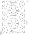
- trench TR extends to constitute a mesh having a honeycomb structure when viewed in a plan view (see Fig. 23 ).
- silicon carbide layer 101 has upper surface P2 having a hexagonal shape and surrounded by trench TR.
- Relaxation region 71 has p type conductivity. Relaxation region 71 is provided in first silicon carbide layer 10. Relaxation region 71 is separated from p base layer 82 by second epitaxial layer 81b. Moreover, relaxation region 71 is separated from each of side wall surface SW and bottom surface BT of trench TR. Preferably, relaxation region 71 is separated from p base layer 82 by not less than 1 ⁇ m and not more than 5 ⁇ m. A value obtained by integrating impurity concentrations based on a unit volume of relaxation region 71 in the thickness direction (vertical direction in Fig. 20 ) corresponds to a dose amount in the ion implantation for forming relaxation region 71.
- This dose amount is preferably not less than 1 ⁇ 10 12 cm -2 and not more than 1 ⁇ 10 15 cm -2 , such as 1 ⁇ 10 13 cm -2 .
- the impurity included in relaxation region 71 is aluminum, for example.
- Relaxation region 71 is at least partially provided in a position deeper than the position of bottom surface BT of trench TR. Preferably, as shown in Fig. 20 , relaxation region 71 is provided only in a position deeper than the position of bottom surface BT of trench TR.
- relaxation region 71 When viewed in a plan view, relaxation region 71 is disposed at least partially outside bottom surface BT of trench TR. Preferably, as shown in Fig. 23 , when viewed in a plan view, relaxation region 71 is disposed only outside bottom surface BT of trench TR. Preferably, when viewed in a plan view ( Fig. 23 ), a distance between relaxation region 71 and bottom surface BT of trench TR is not less than 0.5 ⁇ m and not more than 5 ⁇ m.
- Gate oxide film 91 covers each of side wall surface SW and bottom surface BT of trench TR.
- Gate electrode 92 is provided on gate oxide film 91.
- Source electrode 94 is in contact with each of n regions 83 and p contact region 84.
- Source interconnection layer 95 is in contact with source electrode 94.
- Source interconnection layer 95 is, for example, an aluminum layer.
- Interlayer insulating film 93 insulates between gate electrode 92 and source interconnection layer 95.
- silicon carbide semiconductor device 100 is a MOSFET but silicon carbide semiconductor device 100 is not limited to a MOSFET.
- Silicon carbide semiconductor device 100 may be a Schottky barrier diode or an IGBT (Insulated Gate Bipolar Transistor), for example.
- the first conductivity type is n type and the second conductivity type is p type, but the first conductivity type may be p type and the second conductivity type may be n type.
- the step of performing alignment is used when forming the p contact region, but the step of performing alignment is not limited to the case where it is performed upon the formation of the p contact region.
- the step of performing alignment may be used in a step, such as a silicon carbide dry etching step, a gate electrode forming step, or an interlayer insulating film contact hole forming step.
- second recess 2 is an alignment mark in the exposure process, but second recess 2 is not limited to the alignment mark in the exposure process as long as second recess 2 serves as an alignment mark.
- Second recess 2 may be an alignment mark used for a defect inspection step, a laser annealing step, or the like, for example.
- the ratio obtained by dividing depth D of first recess 1 by thickness T of second silicon carbide layer 20 is more than 0.2. Accordingly, there can be provided a method for manufacturing MOSFET 100 to allow for improved alignment precision.
- a size X1 of an opening 1 a of first recess 1 in an in-plane off direction is less than a size Y1 of opening 1a of first recess 1 in a direction perpendicular to the in-plane off direction. Accordingly, there can be provided a method for manufacturing MOSFET 100 to allow for effectively improved alignment precision.
- size X1 of opening 1a of first recess 1 in in-plane off direction a1 1 is not less than 2 ⁇ m and not more than 15 ⁇ m.
- size X1 of opening 1a is not less than 2 ⁇ m, first recess 1 can be effectively suppressed from being filled.
- size X1 of opening 1a is not more than 15 ⁇ m, opening end portion 1a1 of opening 1a facing opposite to in-plane off direction a1 1 can be suppressed from being reduced in angle.
- second recess 2 is an alignment mark used in an exposure process. Accordingly, in the exposure process, high alignment precision can be realized.
- thickness T of second silicon carbide layer 20 is not less than 0.5 ⁇ m and not more than 5 ⁇ m.
- thickness T of second silicon carbide layer 20 is not less than 0.5 ⁇ m, an effect of increase of on resistance can be suppressed from being strong.
- thickness T of second silicon carbide layer 20 is not more than 5 ⁇ m, first recess 1 can be suppressed effectively from being filled. The electric field relaxation effect of relaxation region 71 can be maintained to be high.
- first recess 1 is formed on a dicing line 3 of first main surface 10a.
- first recess 1 is formed on the dicing line, alignment precision can be improved without decreasing an area in which a semiconductor element is formed.
- the method for manufacturing MOSFET 100 according to the present embodiment further includes a step of forming a first impurity region 71 in first silicon carbide layer 10 after the step of forming first silicon carbide layer 10. Accordingly, MOSFET 100 having relaxation region 71 can be obtained.
- the method for manufacturing MOSFET 100 according to the present embodiment further includes a step of forming a p contact region 84 and a source electrode 94 after the step of performing the alignment based on the image of second recess 2. Accordingly, alignment precision in p contact region 84 and source electrode 94 can be improved.
- silicon carbide epitaxial substrates 10 were prepared each of which was provided with first recess 1 in first main surface 10a as shown in Fig. 3 . Depth D of first recess 1 was set at 0.5 ⁇ m and 1.0 ⁇ m.
- silicon carbide epitaxial substrates 10 projection type substrates
- silicon carbide epitaxial layer 20 having a thickness of 3 mm was formed on first main surface 10a of each of silicon carbide epitaxial substrates 10.
- second recess 2 was formed at a position facing first recess 1 as shown in Fig. 9 .
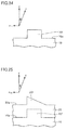
- a second projection 20f was formed at a position facing first projection 10f as shown in Fig. 25 .
- the substrates described above were introduced into an i-line stepper and were aligned using the LSA method and the FIA method, and alignment precision was inspected.
- Table 1 shows results for alignment precision when the LSA method was used, whereas Table 2 shows results for alignment precision when the FIA method was used.
- Table 1 Size Projection Type Recess Type 0.5 ⁇ m Deviation of 2 to 3 ⁇ m to Right Side Deviation of 2 to 3 ⁇ m to Right Side 1.0 ⁇ m Deviation of 2 to 3 ⁇ m to Right Side Deviation of 2 to 3 ⁇ m to Right Side
- Table 2 Size Projection Type Recess Type 0.5 ⁇ m Unrecognizable Unrecognizable 1.0 ⁇ m Unrecognizable Within ⁇ 0.1 ⁇ m
- the recess type is more preferable than the projection type as an alignment mark of a silicon carbide substrate.
- the FIA method is more preferable than the LSA method as an alignment method.
- six types of silicon carbide substrates respectively including first recesses 1 having depths D of 0,6 ⁇ m, 0.7 ⁇ m, 0.8 ⁇ m, 0.9 ⁇ m, and 1.1 ⁇ m were prepared, and then silicon carbide epitaxial layer 20 having a thickness of 3 ⁇ m was formed on each of the silicon carbide substrates.
- first recesses 1 having depths D of 0.5 ⁇ m and 1.0 ⁇ m were prepared, and then silicon carbide epitaxial layer 20 having a thickness of 1.5 ⁇ m was formed on each of the silicon carbide substrates, Using the alignment marks formed in the eight types of silicon carbide substrates in total, alignment precision (read result) was inspected.
- Table 3 shows results for alignment precision when the thickness of silicon carbide epitaxial layer 20 was 3 ⁇ m
- Table 4 shows results for alignment precision when the thickness of silicon carbide epitaxial layer 20 was 1.5 ⁇ m.
- a sign "A” indicates that the alignment marks were read satisfactorily and there were little variations of alignment positions.
- a sign “B” indicates that the alignment marks could be read but there were variations of alignment positions to some extent.
- a sign “C” indicates that the alignment marks could not be read.
Landscapes
- Physics & Mathematics (AREA)
- General Physics & Mathematics (AREA)
- Electrodes Of Semiconductors (AREA)
- Exposure And Positioning Against Photoresist Photosensitive Materials (AREA)
- Exposure Of Semiconductors, Excluding Electron Or Ion Beam Exposure (AREA)
- Recrystallisation Techniques (AREA)
- Engineering & Computer Science (AREA)
- Manufacturing & Machinery (AREA)
Abstract
Description
- The present invention relates to a method for manufacturing a silicon carbide semiconductor device, more particularly, a method for manufacturing a silicon carbide semiconductor device including a step of performing alignment.
- In recent years, in order to achieve high breakdown voltage, low loss, and utilization of semiconductor devices under a high temperature environment, silicon carbide has begun to be adopted as a material for a semiconductor device. Silicon carbide is a wide band gap semiconductor having a band gap larger than that of silicon, which has been conventionally widely used as a material for semiconductor devices. Hence, by adopting silicon carbide as a material for a semiconductor device, the semiconductor device can have a high breakdown voltage, reduced on resistance, and the like. Further, the semiconductor device thus adopting silicon carbide as its material has characteristics less deteriorated even under a high temperature environment than those of a semiconductor device adopting silicon as its material, advantageously.
- For example,
Japanese Patent Laying-Open No. 2011-100928 Japanese Patent Laying-Open No. 2011-100928 - Moreover,
Japanese Patent Laying-Open No. 2013-65650 - Furthermore,
Japanese Patent Laying-Open No. 2009-170558 -
- PTD 1:
Japanese Patent Laying-Open No. 2011-100928 - PTD 2:
Japanese Patent Laying-Open No. 2013-65650 - PTD 3:
Japanese Patent Laying-Open No. 2009-170558 - However, even when a silicon carbide semiconductor device is manufactured using each of the methods described in
Japanese Patent Laying-Open No. 2011-100928 Japanese Patent Laying-Open No. 2013-65650 - Moreover, when the manufacturing method described in
Japanese Patent Laying-Open No. 2009-170558 - A method for manufacturing a silicon carbide semiconductor device according to the present invention has the following steps. There is prepared a first silicon carbide layer having a first main surface and a second main surface opposite to the first main surface. A first recess is formed in the first main surface of the first silicon carbide layer, the first recess including a side portion continuously connected to the first main surface and a bottom portion continuously connected to the side portion. A second silicon carbide layer is formed in contact with the first main surface, the side portion, and the bottom portion, the second silicon carbide layer having a third main surface in contact with the first main surface and a fourth main surface opposite to the third main surface. An image of a second recess formed in the fourth main surface at a position facing the first recess is obtained. Alignment is performed based on the image of the second recess. The first main surface corresponds to a plane angled off relative to a {0001} plane such that a normal line vector of the first main surface has at least one of components of <11-20> and <1-100>. A ratio obtained by dividing a depth of the first recess by a thickness of the second silicon carbide layer is more than 0.2.
- According to the present invention, there can be provided a method for manufacturing a silicon carbide semiconductor device to allow for improved alignment precision.
-
-
Fig. 1 is a schematic plan view schematically showing a first step of a method for manufacturing a silicon carbide semiconductor device according to one embodiment of the present invention. -
Fig. 2 is a schematic cross sectional view schematically showing the first step of the method for manufacturing the silicon carbide semiconductor device according to the embodiment of the present invention. -
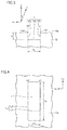
Fig. 3 is a schematic cross sectional view schematically showing a structure of a first recess. -
Fig. 4 is a schematic plan view schematically showing the structure of the first recess. -
Fig. 5 is a schematic cross sectional view schematically showing a second step of the method for manufacturing the silicon carbide semiconductor device according to the embodiment of the present invention. -
Fig. 6 is a schematic plan view schematically showing the structure of the first recess formed on a dicing line. -
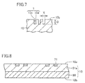
Fig. 7 is a schematic cross sectional view schematically showing a structure of a region VII-VII ofFig, 6 . -
Fig. 8 is a schematic cross sectional view schematically showing a third step of the method for manufacturing the silicon carbide semiconductor device according to the embodiment of the present invention. -
Fig. 9 is a schematic cross sectional view schematically showing a structure of a second recess. -
Fig. 10 is a schematic plan view schematically showing the structure of the second recess. -
Fig. 11 is a schematic cross sectional view schematically showing a fourth step of the method for manufacturing the silicon carbide semiconductor device according to the embodiment of the present invention. -
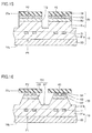
Fig. 12 is a schematic cross sectional view schematically showing a fifth step of the method for manufacturing the silicon carbide semiconductor device according to the embodiment of the present invention. -
Fig. 13 is a schematic cross sectional view schematically showing a sixth step of the method for manufacturing the silicon carbide semiconductor device according to the embodiment of the present invention. -
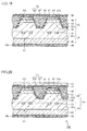
Fig. 14 is a schematic cross sectional view schematically showing a seventh step of the method for manufacturing the silicon carbide semiconductor device according to the embodiment of the present invention. -
Fig. 15 is a schematic cross sectional view schematically showing an eighth step of the method for manufacturing the silicon carbide semiconductor device according to the embodiment of the present invention. -
Fig. 16 is a schematic cross sectional view schematically showing a ninth step of the method for manufacturing the silicon carbide semiconductor device according to the embodiment of the present invention. -
Fig. 17 is a schematic cross sectional view schematically showing a tenth step of the method for manufacturing the silicon carbide semiconductor device according to the embodiment of the present invention. -
Fig. 18 is a schematic cross sectional view schematically showing an eleventh step of the method for manufacturing the silicon carbide semiconductor device according to the embodiment of the present invention. -
Fig. 19 is a schematic cross sectional view schematically showing a twelfth step of the method for manufacturing the silicon carbide semiconductor device according to the embodiment of the present invention. -
Fig. 20 is a schematic cross sectional view schematically showing the structure of the silicon carbide semiconductor device according to the embodiment of the present invention. -
Fig. 21 is a flowchart schematically showing the method for manufacturing the silicon carbide semiconductor device according to the embodiment of the present invention. -
Fig. 22 is a schematic perspective view schematically showing the structure of the silicon carbide layer. -
Fig. 23 is a schematic plan view schematically showing the structure of the silicon carbide layer. -
Fig. 24 is a schematic cross sectional view schematically showing a structure of a first projection according to a comparative example. -
Fig. 25 is a schematic cross sectional view schematically showing a structure of a second projection according to a comparative example. - The following describes an embodiment of the present invention based on figures. It should be noted that in the below-mentioned figures, the same or corresponding portions are given the same reference characters and are not described repeatedly. Regarding crystallographic indications in the present specification, an individual orientation is represented by [], a group orientation is represented by <>, and an individual plane is represented by (), and a group plane is represented by {}. In addition, a negative crystallographic index is normally expressed by putting "-" (bar) above a numeral, but is expressed by putting the negative sign before the numeral in the present specification.
- First, the following describes an overview of embodiments of the present invention.
- As a result of diligent study on a method of forming an alignment mark in a method for manufacturing a silicon carbide semiconductor device, the inventor has obtained the following knowledge and arrived at the present invention. As types of general alignment marks, there are the following two types: a recess type and a projection type. Moreover, as methods of recognizing an alignment mark, there are the following two methods: an LSA (Laser Step Alignment) method and an FIA (Field Image Alignment) method. The LSA method is an optical alignment method in which an alignment mark is irradiated with laser and reflected light of the laser is analyzed for the purpose of alignment. The FIA method is an image recognition method in which an edge of an image recognized by a camera is recognized for the purpose of alignment.
- When forming a silicon carbide epitaxial layer on an angled-off main surface of a silicon carbide substrate, the silicon carbide epitaxial layer is grown asymmetrically with respect to the normal line of the main surface. When forming epitaxial layers on the recess type and projection type alignment marks, a difference in coverage between the epitaxial layers presumably causes a difference in alignment precision between the recess type and the projection type. Similarly, a difference in alignment precision also presumably lies between the LSA method and the FIA method.
- The inventor prepared a silicon carbide substrate having a main surface provided with a recess type groove and a silicon carbide substrate having a main surface provided with a projection type protrusion, then formed silicon carbide epitaxial layers thereon, and then examined alignment precision using the recess and projection formed in the silicon carbide epitaxial layers. For the examination of the alignment precision, each of the LSA method and the FIA method was employed. As a result of the examination, it was found that with the LSA method, a position recognized for alignment is deviated from the actual position in each of the cases of the recess type and the projection type. This is presumably due to the following reason: because the alignment mark itself is deformed asymmetrically, a method employing reflection of light such as the LSA provides offset according to the asymmetrically deformed shape, with the result that the position recognized for alignment is deviated to one side. Next, with the FIA method, the device could not recognize the projection type alignment mark. On the other hand, the device could recognize the recess type alignment mark in some cases, and could not recognize it in other cases.
- As a result of examining the alignment method employing the recess type alignment mark and the FIA method more in detail, the following knowledge was obtained. That is, it was found that when the recess formed in the main surface of the silicon carbide substrate has a small depth, the device cannot recognize the alignment mark; however, when the recess has a large depth, the device can recognize the alignment mark and alignment precision is very high. Moreover, it was found that the alignment precision is affected by not only the depth of the recess but also the thickness of the epitaxial layer formed on the recess. As a result of detailed examination, it was found that high alignment precision is attained when a ratio obtained by dividing the depth of the recess by the thickness of the epitaxial layer formed on the recess is not less than 0.2.
- (1) A method for manufacturing a silicon carbide semiconductor device according to an embodiment includes the following steps. There is prepared a first
silicon carbide layer 10 having a firstmain surface 10a and a secondmain surface 10b opposite to firstmain surface 10a. Afirst recess 1 is formed in firstmain surface 10a of firstsilicon carbide layer 10,first recess 1 including aside portion 10c continuously connected to firstmain surface 10a and abottom portion 10d continuously connected toside portion 10c. A secondsilicon carbide layer 20 is formed in contact with firstmain surface 10a,side portion 10c, andbottom portion 10d, secondsilicon carbide layer 20 having a thirdmain surface 20b in contact with firstmain surface 10a and a fourthmain surface 20a opposite to thirdmain surface 20b. An image of asecond recess 2 formed in fourthmain surface 20a at a position facingfirst recess 1 is obtained. Alignment is performed based on the image ofsecond recess 2. The first main surface corresponds to a plane angled off relative to a {0001} plane such that a normal line vector z of firstmain surface 10a has at least one of components of <11-20> and <1-100>. A ratio obtained by dividing a depth D offirst recess 1 by a thickness T of secondsilicon carbide layer 20 is more than 0.2.
According to the method for manufacturing the silicon carbide semiconductor device according to the embodiment, the ratio obtained by dividing depth D offirst recess 1 by thickness T of secondsilicon carbide layer 20 is more than 0.2. Accordingly, there can be provided a method for manufacturing a silicon carbide semiconductor device to allow for improved alignment precision. - (2) Preferably in the method for manufacturing the silicon carbide semiconductor device according to the embodiment, a size X1 of an
opening 1a offirst recess 1 in an in-plane off direction is less than a size Y1 of opening 1a offirst recess 1 in a direction perpendicular to the in-plane off direction. Accordingly, there can be provided a method for manufacturing a silicon carbide semiconductor device to allow for effectively improved alignment precision. Here, the off direction refers to a direction in which normal line vector z of firstmain surface 10a is inclined relative to a [0001] direction (i.e., c axis). The in-plane off direction refers to a direction obtained by projecting the off direction on firstmain surface 10a. Specific examples of the off direction and the in-plane off direction will be described later. - (3) Preferably in the method for manufacturing the silicon carbide semiconductor device according to the embodiment, size X1 of opening 1a of
first recess 1 in the in-plane off direction is not less than 2 µm and not more than 15 µm. When size X1 ofopening 1a is not less than 2 µm, the first recess can be effectively suppressed from being filled. Moreover, when size X1 ofopening 1a is not more than 15 µm, opening end portion 1a1 ofopening 1a facing opposite to the in-plane off direction can be suppressed from being reduced in angle. - (4) Preferably in the method for manufacturing the silicon carbide semiconductor device according to the embodiment,
second recess 2 is an alignment mark used in an exposure process. Accordingly, in the exposure process, high alignment precision can be realized. - (5) Preferably in the method for manufacturing the silicon carbide semiconductor device according to the embodiment, thickness T of second
silicon carbide layer 20 is not less than 0.5 µm and not more than 5 µm. When thickness T of secondsilicon carbide layer 20 is not less than 0.5 µm, an effect of increase of on resistance can be suppressed from being strong. When thickness T of secondsilicon carbide layer 20 is not more than 5 µm,first recess 1 can be suppressed effectively from being filled. Moreover, when arelaxation region 71 is formed in firstsilicon carbide layer 10, an electric field relaxation effect ofrelaxation region 71 can be maintained to be high. - (6) Preferably in the method for manufacturing the silicon carbide semiconductor device according to the embodiment, in the step of forming
first recess 1,first recess 1 is formed on adicing line 3 of firstmain surface 10a. By formingfirst recess 1 on the dicing line, alignment precision can be increased without decreasing an area in which a semiconductor element is formed. - (7) Preferably, the method for manufacturing the silicon carbide semiconductor device according to the embodiment further includes a step of forming a
first impurity region 71 in firstsilicon carbide layer 10 after the step of forming firstsilicon carbide layer 10. Accordingly, the silicon carbide semiconductor device havingfirst impurity region 71 can be obtained. - (8) Preferably, the method for manufacturing the silicon carbide semiconductor device according to the embodiment further includes a step of forming at least one of a
second impurity region 84 and anelectrode 94 after the step of performing the alignment based on the image of the second recess. Accordingly, alignment precision can be improved for at least one of the second impurity region andelectrode 94. - Next, an embodiment of the present invention will be described more in detail.
- With reference to
Fig. 1 to Fig. 21 , the following describes a method for manufacturing aMOSFET 100 serving as a silicon carbide semiconductor device according to the present embodiment. - First, a first silicon carbide layer forming step (S10:
Fig. 21 ) is performed. Specifically, with reference toFig. 1 and Fig. 2 , a silicon carbidesingle crystal substrate 80 is prepared by slicing an ingot made of, for example, hexagonal silicon carbide having polytype 4H. Next, by epitaxial growth on silicon carbidesingle crystal substrate 80, afirst epitaxial layer 81a made of silicon carbide is formed. This epitaxial growth can be performed by a CVD (Chemical Vapor Deposition) method employing a mixed gas of silane (SiH4) and propane (C3H8) as a source material gas and employing hydrogen gas (H2) as a carrier gas, for example. In doing so, it is preferable to introduce nitrogen (N) or phosphorus (P) as an impurity, for example. As described above, siliconcarbide epitaxial substrate 10 serving as a first silicon carbide layer is prepared. Siliconcarbide epitaxial substrate 10 has n type (first conductivity type). - Silicon
carbide epitaxial substrate 10 has a firstmain surface 10a and a secondmain surface 10b opposite to firstmain surface 10a. Siliconcarbide epitaxial substrate 10 includes: silicon carbidesingle crystal substrate 80; and afirst epitaxial layer 81 a constituted of a silicon carbide epitaxial layer formed on silicon carbidesingle crystal substrate 80, for example. Siliconcarbide epitaxial substrate 10 may be provided with an orientationflat portion 4. When adirection a1 1 in which orientationflat portion 4 extends is a <11-20> direction, a direction a21 perpendicular to direction a11 is a <1-100> direction. Moreover, direction a11 in which orientationflat portion 4 extends is a <1-100> direction, a direction a21 perpendicular todirection a1 1 may be a <11-20> direction, for example. - With reference to
Fig. 2 , firstmain surface 10a corresponds to a plane angled off in off direction a1 by an off angle θ relative to a {0001} plane (plane indicated by a broken line), for example. Off angle θ is preferably an angle of not more than 8°, such as 4° or 8°. Specifically, the first main surface corresponds to a plane angled off relative to the {0001} plane such that a normal line vector z of firstmain surface 10a has at least one of components of <11-20> and <1-100>. Preferably, firstmain surface 10a corresponds to a plane angled off relative to the {0001} plane such that normal line vector z of firstmain surface 10a has a component of <11-20>. InFig. 2 , a direction c is a [0001] direction (i.e., the c axis of the hexagonal silicon carbide), and direction a1 is the <11-20> direction, for example. The off direction is a direction in which normal line vector z of firstmain surface 10a is inclined relative to the [0001] direction. In the case ofFig. 2 , the off direction is the a1 direction (i.e., the <11-20> direction). InFig. 2 , firstmain surface 10a corresponds to a plane obtained by inclining the (0001) plane off relative to the a1 direction. The in-plane off direction represents a direction obtained by projecting the off direction on firstmain surface 10a. In the case ofFig. 2 , the in-plane off direction is the a 11 direction. - Next, a first recess forming step (S20:
Fig. 21 ) is performed. Specifically, with reference toFig. 3 , afirst recess 1 is formed to have an opening in firstmain surface 10a of siliconcarbide epitaxial substrate 10, and includes: aside portion 10c continuously connected to firstmain surface 10a; and abottom portion 10d continuously connected toside portion 10c.First recess 1 has a depth D of, for example, about not less than 0.5 µm and not more than 2 µm, preferably, about not less than 0.7 µm and not more than 1.5 µm, and further preferably, about not less than 0.7 µm and not more than 1.0 µm. Moreover, size X1 of opening 1 a offirst recess 1 in in-plane offdirection a1 1 its, for example, about not less than 2 µm and not more than 15 µm, and preferably about not less than 4 µm and not more than 8 µm. When size X1 is not less than 2 µm, the recess can be suppressed from being filled, whereas when size X1 is not less than 4 µm, the recess is substantially not filled. Moreover, when size X1 is not more than 15 µm, an opening end portion 1a1 offirst recess 1 facing opposite to the a11 direction can be suppressed from being reduced in angle, whereas when size X1 is not more than 8 µm, opening end portion 1a1 facing opposite to the a11 direction, can be substantially securely suppressed from being reduced in angle. - Preferably, with reference to
Fig. 4 , when viewed in a plan view (field of view seen in the normal direction of firstmain surface 10a), size X1 of opening 1a offirst recess 1 in in-plane offdirection a1 1 is smaller than size Y1 of opening 1a offirst recess 1 in direction a12 perpendicular to in-plane off direction a11. Size X1 is 6 µm and size Y1 is 80 µm, for example. Size X1 may be not more than 0.1 time as large as size Y1. - With reference to
Fig. 5 , firstmain surface 10a of siliconcarbide epitaxial substrate 10 may be provided with a plurality ofdicing lines 3 in the a11 direction parallel to the direction in which orientationflat portion 4 extends and the a12 direction perpendicular to the a11 direction. A dicingline 3 represents a cutting position for cutting siliconcarbide epitaxial substrate 10 having semiconductor elements formed thereon. In other words, dicingline 3 represents a position to be cut in a dicing step.Dicing line 3 may be a groove. - With reference to
Fig. 6 andFig. 7 , in the step of forming the first recess,first recess 1 is preferably formed on dicingline 3 of firstmain surface 10a.First recess 1 is preferably formed such that the longitudinal direction of opening 1a of first recess 1 (more preferably, perpendicularly) crosses the direction in which dicingline 3 extends. As shown inFig. 6 , a plurality offirst recesses 1 may be provided in the direction in which the dicing line extends. A space e between two adjacentfirst recesses 1 may be larger or smaller than size X1 offirst recess 1. Space e of two adjacentfirst recesses 1 is about not less than 4 µm and not more than 8 µm, for example. More preferably, a plurality offirst recesses 1 are formed on each of adicing line 3a extending in a direction parallel to the direction in which orientationflat portion 4 extends and adicing line 3b extending in a direction perpendicular to dicingline 3b. - With reference to
Fig. 8 , a relaxation region 71 (first impurity region) having p type (second conductivity type) is formed in contact with a portion of firstmain surface 10a offirst epitaxial layer 81a. Specifically, acceptor ions (impurity ions for providing the second conductivity type) are implanted into firstmain surface 10a offirst epitaxial layer 81a using an implanting mask (not shown). It should be noted thatrelaxation region 71 may be formed after formingfirst recess 1 or may be formed before formingfirst recess 1. - Next, a second silicon carbide layer forming step (S30:
Fig. 21 ) is performed. With reference toFig. 9 to Fig. 11 , afterrelaxation region 71 is formed infirst epitaxial layer 81a, a secondsilicon carbide layer 20 having n type conductivity and made of silicon carbide is formed in contact with firstmain surface 10a of siliconcarbide epitaxial substrate 10. Secondsilicon carbide layer 20 has a thirdmain surface 20b and a fourthmain surface 20a opposite to thirdmain surface 20b. Secondsilicon carbide layer 20 is in contact with firstmain surface 10a,side portion 10c offirst recess 1, andbottom portion 10d offirst recess 1. Thirdmain surface 20b of secondsilicon carbide layer 20 is in contact with firstmain surface 10a. Secondsilicon carbide layer 20 is formed to fillfirst recess 1. Secondsilicon carbide layer 20 has a thickness T of, for example, about not less than 0.5 µm and not more than 5 µm, and preferably, about not less than 1.5 µm and not more than 3 µm. A ratio obtained by dividing depth D offirst recess 1 by thickness T of secondsilicon carbide layer 20 is more than 0.2. The ratio is preferably not less than 0.23, is more preferably not less than 0.27, and is further preferably not less than 0.33. - As shown in
Fig. 9 , asecond recess 2 having an opening in fourthmain surface 20a is formed in fourthmain surface 20a of secondsilicon carbide layer 20 at a position facingfirst recess 1.Second recess 2 includes: afirst side portion 20c and asecond side portion 20e each continuously connected to fourthmain surface 20a; and abottom portion 20d connectingfirst side portion 20c andsecond side portion 20e to each other.Second recess 2 can be used as an alignment mark.First side portion 20c ofsecond recess 2 is formed to correspond to a plane perpendicular to the c axis, for example. - With reference to
Fig. 9 , when viewed in a direction perpendicular to both in-plane offdirection a1 1 and normal line vector z of firstmain surface 10a, opening end portion 2a1 ofsecond recess 2 facing opposite to in-plane offdirection a1 1 in the direction parallel to firstmain surface 10a is formed at a position b1 substantially corresponding to opening end portion 1a1 offirst recess 1. Meanwhile, opening end portion 2a2 ofsecond recess 2 facing in-plane off direction a11 in the direction parallel to firstmain surface 10a is formed at a position b3 substantially corresponding to opening end portion 1a2 offirst recess 1. Hence, the width ofopening 2a ofsecond recess 2 in in-plane off direction a1 1 (i.e., distance between position b1 and position b3) is substantially the same as the width ofopening 1a offirst recess 1 in the in-plane off direction. However, the width ofbottom portion 20d ofsecond recess 2 in in-plane off direction a1 1 (i.e., distance between position b1 and position b2) is less than the width ofbottom portion 10d offirst recess 1 in in-plane off direction a1 1 (i.e., distance between position b1 and position b3). - With reference to
Fig. 10 , size X2 of opening 2a ofsecond recess 2 in in-plane offdirection a1 1 is less than size Y2 of opening 2a ofsecond recess 2 in direction a12 perpendicular to in-plane off direction a11. Moreover, size Y1 of opening 1a offirst recess 1 in direction a12 perpendicular to in-plane offdirection a1 1 is substantially the same as size Y2 of opening 2a ofsecond recess 2 in direction a12 perpendicular to in-plane off direction a11. As described above, position b1 of opening end portion 2a1 ofsecond recess 2 facing opposite to in-plane off direction a11 substantially corresponds to position b1 of opening end portion 1a1 offirst recess 1 facing opposite to in-plane off direction a11, whereby alignment precision can be high by performing alignment using opening end portion 2a1 ofsecond recess 2. Further, when size Y1 of opening 1 a offirst recess 1 in direction a12 perpendicular to the in-plane off direction is increased to be more than size X1 of opening 1a offirst recess 1 in in-plane off direction a11, size Y2 of opening 2a ofsecond recess 2 in direction a12 perpendicular to the in-plane off direction can be increased, thereby effectively improving alignment precision. - With reference to
Fig. 11 , because secondsilicon carbide layer 20 is formed in contact with firstmain surface 10a of siliconcarbide epitaxial substrate 10,relaxation region 71 is buried in first epitaxial layer 81 and secondsilicon carbide layer 20 constituted of first epitaxial layer 81 and secondsilicon carbide layer 20. Secondsilicon carbide layer 20 may be formed by the same method as the method of formingfirst epitaxial layer 81a. - As shown in
Fig. 12 ,a p base layer 82 and ann region 83 are formed in secondsilicon carbide layer 20. Moreover, as shown inFig. 13 ,a p contact region 84 is formed onp base layer 82. They can be formed by means of, for example, ion implantations into the second silicon carbide layer (Fig. 11 ). In the ion implantations for formingp base layer 82 andp contact region 84, ions of an impurity for providing p type such as aluminum (Al) are implanted. Meanwhile, in the ion implantation for formingn region 83, ions of an impurity for providing n type conductivity such as phosphorus (P) are implanted, for example. It should be noted that instead of the ion implantations, epitaxial growth involving addition of impurities may be employed. - Before forming
p contact region 84, a second recess image obtaining step (S40:Fig. 21 ) and an alignment step (S50:Fig. 21 ) may be performed. Specifically, an image ofsecond recess 2 formed in fourthmain surface 20a of secondsilicon carbide layer 20 at the position facingfirst recess 1 is obtained. The image ofsecond recess 2 may be obtained by, for example, a camera and an edge ofsecond recess 2 may be recognized. The edge ofsecond recess 2 is, for example, opening end portion 2a1 of opening 2a ofsecond recess 2 facing opposite to the in-plane off direction (seeFig. 10 ). Next, alignment is performed based on the image ofsecond recess 2.Second recess 2 is an alignment mark used in an exposure process, for example. Specifically, the position of siliconcarbide epitaxial substrate 10 having secondsilicon carbide layer 20 formed thereon is adjusted such that a mask layer formed of, for example, a resist is formed on fourthmain surface 20a and the mask layer above a region in whichp contact region 84 is to be formed is exposed. Next, the mask layer is subjected to exposure and development, thereby removing a portion of the mask layer above the region in whichp contact region 84 is to be formed. Next, ions are implanted into secondsilicon carbide layer 20 using the remaining mask layer, thereby formingp contact region 84. As described above, p contact region 84 (second impurity region) is formed after alignment is performed based on the image ofsecond recess 2. In the manner described above, the relative position ofp contact region 84 torelaxation region 71 in the in-plane direction of fourthmain surface 20a may be adjusted. - Next, heat treatment is performed to activate the impurities. This heat treatment is preferably performed at a temperature of not less than 1500°C and not more than 1900°C, such as a temperature of approximately 1700°C. The heat treatment is performed for approximately 30 minutes, for example. The atmosphere of the heat treatment is preferably an inert gas atmosphere, such as Ar atmosphere.
- As shown in
Fig. 14 , amask layer 40 having an opening is formed on fourthmain surface 20a constituted ofn region 83 andp contact region 84. Asmask layer 40, a silicon oxide film or the like can be used, for example. The opening is formed corresponding to the position of a trench TR (seeFig. 20 ). Based on the image ofsecond recess 2 formed in secondsilicon carbide layer 20,mask layer 40 may be aligned and formed such that a position corresponding to the opening is exposed. - As shown in
Fig. 15 , in the opening ofmask layer 40,n region 83,p base layer 82, and a portion ofsecond epitaxial layer 81b are removed by etching. An exemplary, usable etching method is reactive ion etching (RIE), in particular, inductively coupled plasma (ICP) RIE Specifically, for example, ICP-RIE can be used which employs SF6 or a mixed gas of SF6 and O2 as a reactive gas. With such etching, in the region in which trench TR (seeFig. 20 ) is to be formed, a recess TQ is formed to have a side wall substantially perpendicular to upper surface P2 (i.e., fourthmain surface 20a). - Next, thermal etching is performed in recess TQ. For example, the thermal etching can be performed by heating in an atmosphere including a reactive gas having at least one or more types of halogen atom. The at least one or more types of halogen atom include at least one of chlorine (Cl) atom and fluorine (F) atom. This atmosphere is Cl2, BCL3, SF6, or CF4, for example. For example, the thermal etching is performed using a mixed gas of chlorine gas and oxygen gas as a reactive gas, at a heat treatment temperature of, for example, not less than 700°C and not more than 1000°C.
- It should be noted that the reactive gas may contain a carrier gas in addition to the chlorine gas and the oxygen gas. An exemplary, usable carrier gas is nitrogen (N2) gas, argon gas, helium gas, or the like. When the heat treatment temperature is set at not less than 700°C and not more than 1000°C as described above, a rate of etching silicon carbide is approximately, for example, 70 µm/hour. In addition, in this case,
mask layer 40, which is formed of silicon oxide and therefore has a very large selection ratio relative to silicon carbide, is not substantially etched during the etching of silicon carbide. - As shown in
Fig. 16 , by the thermal etching, trench TR is formed in upper surface P2 ofsilicon carbide layer 101. Trench TR includes: a side wall surface SW extending tosecond epitaxial layer 81b throughn region 83 andp base layer 82; and a bottom surface BT located onsecond epitaxial layer 81b. Each of side wall surface SW and bottom surface BT is separated fromrelaxation region 71. Next,mask layer 40 is removed by means of an appropriate method such as etching (Fig. 22 ). - As shown in
Fig. 17 ,gate oxide film 91 is formed to cover each of side wall surface SW and bottom surface BT of trench TR.Gate oxide film 91 can be formed by means of, for example, thermal oxidation. Thereafter, NO annealing may be performed using nitrogen monoxide (NO) gas as an atmospheric gas. A temperature profile has such a condition that the temperature is not less than 1100°C and not more than 1300°C and holding time is approximately 1 hour, for example. Accordingly, nitrogen atoms are introduced in an interface region betweengate oxide film 91 andp base layer 82. As a result, formation of interface states in the interface region is suppressed, thereby achieving improved channel mobility. It should be noted that a gas other than the NO gas can be employed as the atmospheric gas as long as the nitrogen atoms can be thus introduced. After this NO annealing, Ar annealing may be further performed using argon (Ar) as an atmospheric gas. The Ar annealing is preferably performed at a heating temperature higher than the heating temperature in the above-described NO annealing and lower than the melting point ofgate oxide film 91. This heating temperature is held for approximately 1 hour, for example. Accordingly, formation of interface states in the interface region betweengate oxide film 91 andp base layer 82 is further suppressed. It should be noted that instead of the Ar gas, an inert gas such as nitrogen gas can be employed as the atmospheric gas. - As shown in
Fig. 18 ,gate electrode 92 is formed ongate oxide film 91. Specifically,gate electrode 92 is formed ongate oxide film 91 so as to fill the region within trench TR withgate oxide film 91 interposed therebetween. A method for forminggate electrode 92 can be performed by, for example, forming a film of conductor or doped polysilicon and performing CMP (Chemical Mechanical Polishing). - With reference to
Fig. 19 , aninterlayer insulating film 93 is formed ongate electrode 92 andgate oxide film 91 so as to cover the exposed surface ofgate electrode 92. Etching is performed to form an opening ininterlayer insulating film 93 andgate oxide film 91. Through the opening, each ofn region 83 andp contact region 84 is exposed on upper surface P2. The opening may be formed after performing alignment based on the image ofsecond recess 2 formed in secondsilicon carbide layer 20 and then performing the exposure and development processes. Next, on upper surface P2, asource electrode 94 is formed in contact with each ofn region 83 andn contact region 84. Adrain electrode 98 is formed on lower surface P1 constituted of first epitaxial layer 81 with silicon carbidesingle crystal substrate 80 being interposed therebetween. - With reference to
Fig. 20 , asource interconnection layer 95 is formed. In this way,MOSFET 100 is completed which serves as a silicon carbide semiconductor device and which includessilicon carbide layer 101,gate oxide film 91,gate electrode 92,interlayer insulating film 93,source electrode 94,source interconnection layer 95, and drainelectrode 98.Silicon carbide layer 101 has a hexagonal crystal structure of polytype 4H.Silicon carbide layer 101 includes firstsilicon carbide layer 10 and secondsilicon carbide layer 20. Firstsilicon carbide layer 10 includes silicon carbidesingle crystal substrate 80,first epitaxial layer 81a, andrelaxation region 71. Secondsilicon carbide layer 20 includessecond epitaxial layer 81b,p base layer 82,n region 83, andp contact region 84. - Each of
first epitaxial layer 81 a andsecond epitaxial layer 81b has n type conductivity. Each offirst epitaxial layer 81a andsecond epitaxial layer 81b preferably has an impurity concentration lower than the impurity concentration of silicon carbidesingle crystal substrate 80. Each offirst epitaxial layer 81a andsecond epitaxial layer 81b preferably has a donor concentration of not less than 1 × 1015cm-3 and not more than 5 × 1016cm-3, such as 8 × 1015 cm-3. -
P base layer 82 has p type.P base layer 82 is provided onsecond epitaxial layer 81b.P base layer 82 has an acceptor concentration of, for example, 1 × 1018cm-3.N region 83 has n type conductivity.N region 83 is provided onp base layer 82 so as to be separated fromsecond epitaxial layer 81b byp base layer 82.N region 83 andp contact region 84 constitute upper surface P2 ofsilicon carbide layer 101.P contact region 84 has p type conductivity.P contact region 84 is connected top base layer 82. - Trench TR is provided in upper surface P2 of
silicon carbide layer 101. Trench TR has a side wall surface SW and a bottom surface BT. Side wall surface SW extends tosecond epitaxial layer 81b throughn region 83 andp base layer 82. Side wall surface SW includes a channel surface ofMOSFET 100 onp base layer 82. Side wall surface SW is inclined relative to upper surface P2 ofsilicon carbide layer 101, whereby trench TR is expanded toward the opening in a tapered manner. Side wall surface SW preferably has a plane orientation inclined by not less than 50° and not more than 65° relative to the {0001} plane, and more preferably has a plane orientation inclined by not less than 50° and not more than 65° relative to the (000-1) plane. - Bottom surface BT is located on
second epitaxial layer 81 b. In the present embodiment, bottom surface BT has a flat shape substantially parallel to upper surface P2. A portion at which bottom surface BT and side wall surface SW are connected to each other constitutes a corner portion of trench TR. In the present embodiment, trench TR extends to constitute a mesh having a honeycomb structure when viewed in a plan view (seeFig. 23 ). Accordingly,silicon carbide layer 101 has upper surface P2 having a hexagonal shape and surrounded by trench TR. -
Relaxation region 71 has p type conductivity.Relaxation region 71 is provided in firstsilicon carbide layer 10.Relaxation region 71 is separated fromp base layer 82 bysecond epitaxial layer 81b. Moreover,relaxation region 71 is separated from each of side wall surface SW and bottom surface BT of trench TR. Preferably,relaxation region 71 is separated fromp base layer 82 by not less than 1 µm and not more than 5 µm. A value obtained by integrating impurity concentrations based on a unit volume ofrelaxation region 71 in the thickness direction (vertical direction inFig. 20 ) corresponds to a dose amount in the ion implantation for formingrelaxation region 71. This dose amount is preferably not less than 1 × 1012cm-2 and not more than 1 × 1015cm-2, such as 1 × 1013 cm-2. The impurity included inrelaxation region 71 is aluminum, for example.Relaxation region 71 is at least partially provided in a position deeper than the position of bottom surface BT of trench TR. Preferably, as shown inFig. 20 ,relaxation region 71 is provided only in a position deeper than the position of bottom surface BT of trench TR. - When viewed in a plan view,
relaxation region 71 is disposed at least partially outside bottom surface BT of trench TR. Preferably, as shown inFig. 23 , when viewed in a plan view,relaxation region 71 is disposed only outside bottom surface BT of trench TR. Preferably, when viewed in a plan view (Fig. 23 ), a distance betweenrelaxation region 71 and bottom surface BT of trench TR is not less than 0.5 µm and not more than 5 µm. -
Gate oxide film 91 covers each of side wall surface SW and bottom surface BT of trench TR.Gate electrode 92 is provided ongate oxide film 91.Source electrode 94 is in contact with each ofn regions 83 andp contact region 84.Source interconnection layer 95 is in contact withsource electrode 94.Source interconnection layer 95 is, for example, an aluminum layer.Interlayer insulating film 93 insulates betweengate electrode 92 andsource interconnection layer 95. - In the above-mentioned embodiment, it has been illustrated that silicon
carbide semiconductor device 100 is a MOSFET but siliconcarbide semiconductor device 100 is not limited to a MOSFET. Siliconcarbide semiconductor device 100 may be a Schottky barrier diode or an IGBT (Insulated Gate Bipolar Transistor), for example. In the example, it has been illustrated that the first conductivity type is n type and the second conductivity type is p type, but the first conductivity type may be p type and the second conductivity type may be n type. In the above-mentioned embodiment, it has been illustrated that the step of performing alignment is used when forming the p contact region, but the step of performing alignment is not limited to the case where it is performed upon the formation of the p contact region. The step of performing alignment may be used in a step, such as a silicon carbide dry etching step, a gate electrode forming step, or an interlayer insulating film contact hole forming step. - Moreover, in the above-mentioned embodiment, it has been illustrated that
second recess 2 is an alignment mark in the exposure process, butsecond recess 2 is not limited to the alignment mark in the exposure process as long assecond recess 2 serves as an alignment mark.Second recess 2 may be an alignment mark used for a defect inspection step, a laser annealing step, or the like, for example. - Next, the following describes function and effect of the method for manufacturing
MOSFET 100 according to the present embodiment. - According to the method for manufacturing
MOSFET 100 according to the present embodiment, the ratio obtained by dividing depth D offirst recess 1 by thickness T of secondsilicon carbide layer 20 is more than 0.2. Accordingly, there can be provided a method for manufacturingMOSFET 100 to allow for improved alignment precision. - Moreover, according to the method for manufacturing
MOSFET 100 according to the present embodiment, a size X1 of anopening 1 a offirst recess 1 in an in-plane off direction is less than a size Y1 of opening 1a offirst recess 1 in a direction perpendicular to the in-plane off direction. Accordingly, there can be provided a method for manufacturingMOSFET 100 to allow for effectively improved alignment precision. - Moreover, according to the method for manufacturing
MOSFET 100 according to the present embodiment, size X1 of opening 1a offirst recess 1 in in-plane offdirection a1 1 is not less than 2 µm and not more than 15 µm. When size X1 ofopening 1a is not less than 2 µm,first recess 1 can be effectively suppressed from being filled. Moreover, when size X1 ofopening 1a is not more than 15 µm, opening end portion 1a1 ofopening 1a facing opposite to in-plane offdirection a1 1 can be suppressed from being reduced in angle. - Moreover, according to the method for manufacturing
MOSFET 100 according to the present embodiment,second recess 2 is an alignment mark used in an exposure process. Accordingly, in the exposure process, high alignment precision can be realized. - Moreover, according to the method for manufacturing
MOSFET 100 according to the present embodiment, thickness T of secondsilicon carbide layer 20 is not less than 0.5 µm and not more than 5 µm. When thickness T of secondsilicon carbide layer 20 is not less than 0.5 µm, an effect of increase of on resistance can be suppressed from being strong. When thickness T of secondsilicon carbide layer 20 is not more than 5 µm,first recess 1 can be suppressed effectively from being filled. The electric field relaxation effect ofrelaxation region 71 can be maintained to be high. - Moreover, according to the method for manufacturing
MOSFET 100 according to the present embodiment, in the step of formingfirst recess 1,first recess 1 is formed on adicing line 3 of firstmain surface 10a. By formingfirst recess 1 on the dicing line, alignment precision can be improved without decreasing an area in which a semiconductor element is formed. - Moreover, the method for manufacturing
MOSFET 100 according to the present embodiment further includes a step of forming afirst impurity region 71 in firstsilicon carbide layer 10 after the step of forming firstsilicon carbide layer 10. Accordingly,MOSFET 100 havingrelaxation region 71 can be obtained. - Moreover, the method for manufacturing
MOSFET 100 according to the present embodiment further includes a step of forminga p contact region 84 and asource electrode 94 after the step of performing the alignment based on the image ofsecond recess 2. Accordingly, alignment precision inp contact region 84 andsource electrode 94 can be improved. - First, silicon carbide epitaxial substrates 10 (recess type substrate) were prepared each of which was provided with
first recess 1 in firstmain surface 10a as shown inFig. 3 . Depth D offirst recess 1 was set at 0.5 µm and 1.0 µm. Likewise, silicon carbide epitaxial substrates 10 (projection type substrates) were prepared each of which was provided with afirst projection 10f at firstmain surface 10a as shown inFig. 24 . The height offirst projection 10f was set at 0.5 µm and 1.0 µm. Next, siliconcarbide epitaxial layer 20 having a thickness of 3 mm was formed on firstmain surface 10a of each of siliconcarbide epitaxial substrates 10. When the recess type substrate was used,second recess 2 was formed at a position facingfirst recess 1 as shown inFig. 9 . When the projection type substrate was used, asecond projection 20f was formed at a position facingfirst projection 10f as shown inFig. 25 . In this way, the following two types of substrates were prepared: the substrate (projection type) according to a comparative example; and the substrate (recess type) according to the present invention's example. The substrates described above were introduced into an i-line stepper and were aligned using the LSA method and the FIA method, and alignment precision was inspected. - With reference to Table 1 and Table 2, the following describes results for alignment precision. Table 1 shows results for alignment precision when the LSA method was used, whereas Table 2 shows results for alignment precision when the FIA method was used.
[Table 1] Size Projection Type Recess Type 0.5 µm Deviation of 2 to 3 µm to Right Side Deviation of 2 to 3 µm to Right Side 1.0 µm Deviation of 2 to 3 µm to Right Side Deviation of 2 to 3 µm to Right Side [Table 2] Size Projection Type Recess Type 0.5 µm Unrecognizable Unrecognizable 1.0 µm Unrecognizable Within ±0.1 µm - As shown in Table 1, when the LSA method was used, the alignment position was deviated by about 2 to 3 µm to one side (right side) in the case of each of the projection type substrate and the recess type substrate. No difference was found between the case where each of depth D of
first recess 1 and the height offirst projection 10f was 0.5 µm and the case where each of depth D offirst recess 1 and the height offirst projection 10f was 1.0 µm. When the alignment mark itself is deformed asymmetrically, a method employing reflection of light such as the LSA method presumably provides offset according to the deformed shape, thus resulting in uniform deviation to one side. - As shown in Table 2, when the FIA method was used and each of depth D of
first recess 1 and the height offirst projection 10f was 0.5 µm, the stepper could not recognize the alignment mark in the case of each of the projection type substrate and the recess type substrate before performing alignment. Moreover, for the projection type substrate havingfirst projection 1 0f having a height of 1.0 µm, the stepper could not recognize the alignment mark. On the other hand, when depth D offirst recess 1 was 1.0 µm, alignment precision was ±0.1 µm. This alignment precision was comparable to alignment precision guaranteed for a reference mark by the i-line stepper used for this experiment. - In this way, it was confirmed that the recess type is more preferable than the projection type as an alignment mark of a silicon carbide substrate. Moreover, it was confirmed that the FIA method is more preferable than the LSA method as an alignment method.
- Next, alignment precision was checked by changing the depth of
first recess 1 and thickness T of siliconcarbide epitaxial layer 20 formed onfirst recess 1. Specifically, six types of silicon carbide substrates respectively includingfirst recesses 1 having depths D of 0,6 µm, 0.7 µm, 0.8 µm, 0.9 µm, and 1.1 µm were prepared, and then siliconcarbide epitaxial layer 20 having a thickness of 3 µm was formed on each of the silicon carbide substrates. Likewise, two types of silicon carbide substrates includingfirst recesses 1 having depths D of 0.5 µm and 1.0 µm were prepared, and then siliconcarbide epitaxial layer 20 having a thickness of 1.5 µm was formed on each of the silicon carbide substrates, Using the alignment marks formed in the eight types of silicon carbide substrates in total, alignment precision (read result) was inspected. - With reference to Table 3 and Table 4, the following describes results for alignment precision. Table 3 shows results for alignment precision when the thickness of silicon
carbide epitaxial layer 20 was 3 µm, whereas Table 4 shows results for alignment precision when the thickness of siliconcarbide epitaxial layer 20 was 1.5 µm. Here, the definitions of signs in the read results will be described. A sign "A" indicates that the alignment marks were read satisfactorily and there were little variations of alignment positions. A sign "B" indicates that the alignment marks could be read but there were variations of alignment positions to some extent. A sign "C" indicates that the alignment marks could not be read.[Table 3] Depth (D) of First Recess 0.6 µm 0.7 µm 0.8 µm 0.9 µm 1.1 µm Thickness (T) of Second Silicon Carbide Layer 3 µm 3 µm 3 µm 3 µm 3 µm Ratio(D/T) 0.20 0.23 0.27 0.3 0.37 Read Result C B A A A [Table 4] Depth (D) of First Recess 0.5 µm 1.0 µm Thickness (T) of Second Silicon Carbide Layer 1.5 µm 1.5 µm Ratio (D/T) 0.33 0.67 Read Result A A - As shown in Table 3 and Table 4, it was confirmed that when a ratio obtained by dividing depth D of
first recess 1 by the second silicon carbide layer (silicon carbide epitaxial layer) is more than 0.2, more specifically, when the ratio is not less than 0.23, the alignment marks can be read although there are variations of alignment positions to some extent. Moreover, it was confirmed that when the ratio is not less than 0.27, the alignment marks are read satisfactorily and there are little variations of alignment positions. Furthermore, it was confirmed that when the ratio is not less than 0.33, even if the thickness of siliconcarbide epitaxial layer 20 is 1.5 µm, the alignment marks are read satisfactorily and there are little variations of alignment positions. - The embodiments and examples disclosed herein are illustrative and non-restrictive in any respect. The scope of the present invention is defined by the terms of the claims, rather than the embodiments described above, and is intended to include any modifications within the scope and meaning equivalent to the terms of the claims.
-
- 1: first recess; 1a1, 1a2, 2a1, 2a2: opening end portion; 1a, 2a: opening; 2: second recess; 3, 3a, 3b: dicing line; 4: orientation flat portion; 10: first silicon carbide layer (silicon carbide epitaxial substrate); 10a: first main surface; 10b: second main surface; 10c: side portion; 10d, 20d: bottom portion; 10f: first projection; 20: second silicon carbide layer (silicon carbide epitaxial layer); 20a: fourth main surface; 20b: third main surface; 20c: first side portion; 20e: second side portion; 20f: second projection; 40: mask layer; 71: relaxation region (first impurity region); 80: silicon carbide single crystal substrate; 81a: first epitaxial layer; 81b: second epitaxial layer; 82: p base layer; 83: n region; 84: p contact region (second impurity region); 91: gate oxide film; 92: gate electrode; 93: interlayer insulating film; 94: source electrode; 95: source interconnection layer; 98: drain electrode; 100: MOSFET; 101: silicon carbide layer; BT: bottom surface; P1: lower surface; P2: upper surface; SW: side wall surface; T: thickness; TQ: recess; TR: trench; W: width; e: space; a1: off direction; a11: in-plane off direction; b1, b2, b3: position; z: normal line vector.
Claims (8)
- A method for manufacturing a silicon carbide semiconductor device, comprising steps of:preparing a first silicon carbide layer having a first main surface and a second main surface opposite to said first main surface;forming a first recess in said first main surface of said first silicon carbide layer, said first recess including a side portion continuously connected to said first main surface and a bottom portion continuously connected to said side portion;forming a second silicon carbide layer in contact with said first main surface, said side portion, and said bottom portion, said second silicon carbide layer having a third main surface in contact with said first main surface and a fourth main surface opposite to said third main surface;obtaining an image of a second recess formed in said fourth main surface at a position facing said first recess; andperforming alignment based on said image of said second recess,said first main surface corresponding to a plane angled off relative to a {0001 } plane such that a normal line vector of said first main surface has at least one of components of <11-20> and <1-100>,a ratio obtained by dividing a depth of said first recess by a thickness of said second silicon carbide layer being more than 0.2.
- The method for manufacturing the silicon carbide semiconductor device according to claim 1, wherein a size of an opening of said first recess in an in-plane off direction is less than a size of said opening of said first recess in a direction perpendicular to said in-plane off direction.
- The method for manufacturing the silicon carbide semiconductor device according to claim 2, wherein the size of the opening of said first recess in said in-plane off direction is not less than 2 µm and not more than 15 µm.
- The method for manufacturing the silicon carbide semiconductor device according to any one of claims 1 to 3, wherein said second recess is an alignment mark used in an exposure process.
- The method for manufacturing the silicon carbide semiconductor device according to any one of claims 1 to 4, wherein the thickness of said second silicon carbide layer is not less than 0.5 µm and not more than 5 µm.
- The method for manufacturing the silicon carbide semiconductor device according to any one of claims 1 to 5, wherein in the step of forming said first recess, said first recess is formed on a dicing line of said first main surface.
- The method for manufacturing the silicon carbide semiconductor device according to any one of claims 1 to 6, further comprising a step of forming a first impurity region in said first silicon carbide layer after the step of forming said first silicon carbide layer.
- The method for manufacturing the silicon carbide semiconductor device according to any one of claims 1 to 7, further comprising a step of forming at least one of a second impurity region and an electrode after the step of performing the alignment based on said image of said second recess.
Applications Claiming Priority (2)
| Application Number | Priority Date | Filing Date | Title |
|---|---|---|---|
| JP2013124657A JP6107453B2 (en) | 2013-06-13 | 2013-06-13 | Method for manufacturing silicon carbide semiconductor device |
| PCT/JP2014/062311 WO2014199749A1 (en) | 2013-06-13 | 2014-05-08 | Silicon carbide semiconductor device manufacturing method |
Publications (2)
| Publication Number | Publication Date |
|---|---|
| EP3010037A1 true EP3010037A1 (en) | 2016-04-20 |
| EP3010037A4 EP3010037A4 (en) | 2017-03-22 |
Family
ID=52022051
Family Applications (1)
| Application Number | Title | Priority Date | Filing Date |
|---|---|---|---|
| EP14810167.8A Withdrawn EP3010037A4 (en) | 2013-06-13 | 2014-05-08 | Silicon carbide semiconductor device manufacturing method |
Country Status (5)
| Country | Link |
|---|---|
| US (1) | US9620358B2 (en) |
| EP (1) | EP3010037A4 (en) |
| JP (1) | JP6107453B2 (en) |
| CN (1) | CN105283947A (en) |
| WO (1) | WO2014199749A1 (en) |
Families Citing this family (13)
| Publication number | Priority date | Publication date | Assignee | Title |
|---|---|---|---|---|
| JP6331634B2 (en) * | 2014-04-17 | 2018-05-30 | 住友電気工業株式会社 | Method for manufacturing silicon carbide semiconductor device |
| CN105047536A (en) * | 2015-07-22 | 2015-11-11 | 泰科天润半导体科技(北京)有限公司 | Alignment mark for silicon carbide device and preparation method of alignment mark |
| JP2017055007A (en) * | 2015-09-11 | 2017-03-16 | 株式会社東芝 | Semiconductor device and manufacturing method thereof |
| WO2017090285A1 (en) | 2015-11-24 | 2017-06-01 | 住友電気工業株式会社 | Method for manufacturing silicon carbide epitaxial substrate and silicon carbide semiconductor device |
| JP6472776B2 (en) * | 2016-02-01 | 2019-02-20 | 富士電機株式会社 | Silicon carbide semiconductor device and method for manufacturing silicon carbide semiconductor device |
| DE102016226237B4 (en) | 2016-02-01 | 2024-07-18 | Fuji Electric Co., Ltd. | SILICON CARBIDE SEMICONDUCTOR DEVICE |
| JP6705670B2 (en) * | 2016-03-15 | 2020-06-03 | 富士電機株式会社 | Silicon carbide semiconductor device and method for manufacturing silicon carbide semiconductor device |
| JP2019056725A (en) * | 2017-09-19 | 2019-04-11 | 株式会社デンソー | Method for manufacturing semiconductor device using silicon carbide semiconductor substrate |
| JP6950396B2 (en) * | 2017-09-19 | 2021-10-13 | 株式会社デンソー | Silicon Carbide Semiconductor Substrate and Method for Manufacturing Silicon Carbide Semiconductor Device Using It |
| JP6981890B2 (en) * | 2018-01-29 | 2021-12-17 | ルネサスエレクトロニクス株式会社 | Semiconductor device |
| WO2020250678A1 (en) * | 2019-06-13 | 2020-12-17 | 住友電気工業株式会社 | Silicon carbide substrate and silicon carbide substrate production method |
| US11978677B2 (en) * | 2021-06-24 | 2024-05-07 | Taiwan Semiconductor Manufacturing Co., Ltd. | Wafer positioning method and apparatus |
| JP7640486B2 (en) * | 2022-03-08 | 2025-03-05 | 株式会社デンソー | Semiconductor device manufacturing method and semiconductor wafer |
Family Cites Families (27)
| Publication number | Priority date | Publication date | Assignee | Title |
|---|---|---|---|---|
| US5072266A (en) * | 1988-12-27 | 1991-12-10 | Siliconix Incorporated | Trench DMOS power transistor with field-shaping body profile and three-dimensional geometry |
| JPH04255211A (en) * | 1991-02-07 | 1992-09-10 | Nec Kyushu Ltd | Semiconductor wafer with alignment mark |
| JP3590940B2 (en) * | 1995-04-27 | 2004-11-17 | 株式会社ニコン | Alignment device and exposure device |
| JPH1038514A (en) * | 1996-07-23 | 1998-02-13 | Nikon Corp | Position detection device |
| JP3638250B2 (en) * | 2000-10-11 | 2005-04-13 | シャープ株式会社 | Alignment mark and method for manufacturing semiconductor device |
| JP4110875B2 (en) * | 2002-08-09 | 2008-07-02 | 株式会社デンソー | Silicon carbide semiconductor device |
| JP3989869B2 (en) * | 2003-04-14 | 2007-10-10 | 沖電気工業株式会社 | Semiconductor device and manufacturing method thereof |
| KR101642670B1 (en) * | 2003-07-28 | 2016-07-25 | 가부시키가이샤 니콘 | Exposure apparatus, device producing method, and exposure apparatus controlling method |
| SE527205C2 (en) * | 2004-04-14 | 2006-01-17 | Denso Corp | Process for manufacturing semiconductor device with channel in silicon carbide semiconductor substrate |
| JP4830285B2 (en) * | 2004-11-08 | 2011-12-07 | 株式会社デンソー | Method for manufacturing silicon carbide semiconductor device |
| JP4531713B2 (en) * | 2006-03-31 | 2010-08-25 | 三菱電機株式会社 | Alignment mark and method for forming the same, semiconductor device and method for manufacturing the same |
| JP2007281157A (en) | 2006-04-06 | 2007-10-25 | Mitsubishi Electric Corp | Manufacturing method of semiconductor device |
| US7595241B2 (en) * | 2006-08-23 | 2009-09-29 | General Electric Company | Method for fabricating silicon carbide vertical MOSFET devices |
| JP2008053363A (en) * | 2006-08-23 | 2008-03-06 | Matsushita Electric Ind Co Ltd | Semiconductor substrate and manufacturing method thereof |
| JP5098294B2 (en) * | 2006-10-30 | 2012-12-12 | 株式会社デンソー | Method for manufacturing silicon carbide semiconductor device |
| JP2007201499A (en) * | 2007-04-06 | 2007-08-09 | Denso Corp | Semiconductor substrate and manufacturing method thereof |
| JP4924440B2 (en) | 2008-01-14 | 2012-04-25 | 株式会社デンソー | Method for manufacturing silicon carbide semiconductor device |
| US7691711B2 (en) * | 2008-01-31 | 2010-04-06 | General Electric Company | Method for fabricating silicon carbide vertical MOSFET devices |
| US7906427B2 (en) * | 2008-10-14 | 2011-03-15 | General Electric Company | Dimension profiling of SiC devices |
| JP5240164B2 (en) | 2009-11-09 | 2013-07-17 | 株式会社デンソー | Method for manufacturing silicon carbide semiconductor device |
| KR101331420B1 (en) * | 2011-03-04 | 2013-11-21 | 가부시키가이샤 히다치 고쿠사이 덴키 | Substrate processing apparatus and method of manufacturing semiconductor device |
| JP2013065650A (en) | 2011-09-16 | 2013-04-11 | Mitsubishi Electric Corp | Silicon carbide semiconductor device manufacturing method |
| JP5209152B1 (en) * | 2011-09-22 | 2013-06-12 | パナソニック株式会社 | Silicon carbide semiconductor device and manufacturing method thereof |
| DE112013004362B4 (en) * | 2012-09-06 | 2018-06-21 | Mitsubishi Electric Corporation | SEMICONDUCTOR DEVICE |
| CN102945842B (en) * | 2012-11-21 | 2016-12-21 | 上海华虹宏力半导体制造有限公司 | Alignment mark and manufacture method thereof |
| KR20150109388A (en) * | 2013-01-22 | 2015-10-01 | 피에스5 뤽스코 에스.에이.알.엘. | Method for manufacturing semiconductor device |
| JP6178106B2 (en) * | 2013-04-25 | 2017-08-09 | 住友電気工業株式会社 | Method for manufacturing silicon carbide semiconductor device |
-
2013
- 2013-06-13 JP JP2013124657A patent/JP6107453B2/en active Active
-
2014
- 2014-05-08 CN CN201480032882.8A patent/CN105283947A/en active Pending
- 2014-05-08 US US14/892,972 patent/US9620358B2/en active Active
- 2014-05-08 WO PCT/JP2014/062311 patent/WO2014199749A1/en not_active Ceased
- 2014-05-08 EP EP14810167.8A patent/EP3010037A4/en not_active Withdrawn
Also Published As
| Publication number | Publication date |
|---|---|
| CN105283947A (en) | 2016-01-27 |
| US9620358B2 (en) | 2017-04-11 |
| JP6107453B2 (en) | 2017-04-05 |
| US20160118250A1 (en) | 2016-04-28 |
| JP2015002198A (en) | 2015-01-05 |
| WO2014199749A1 (en) | 2014-12-18 |
| EP3010037A4 (en) | 2017-03-22 |
Similar Documents
| Publication | Publication Date | Title |
|---|---|---|
| US9620358B2 (en) | Method for manufacturing silicon carbide semiconductor device | |
| US9263347B2 (en) | Method of manufacturing silicon carbide semiconductor device | |
| US20170012108A1 (en) | Method for manufacturing semiconductor device | |
| CN103890952B (en) | Sic semiconductor device and manufacture method thereof | |
| JP5828568B1 (en) | Semiconductor device and manufacturing method thereof | |
| WO2015015937A1 (en) | Production method for silicon carbide semiconductor device | |
| EP2400527A1 (en) | Silicon carbide substrate and method for production thereof | |
| US20160204206A1 (en) | Silicon carbide semiconductor device and method for manufacturing same | |
| WO2014073127A1 (en) | Semiconductor device and production method for same | |
| US8809945B2 (en) | Semiconductor device having angled trench walls | |
| JP6287193B2 (en) | Method for manufacturing silicon carbide semiconductor device | |
| US9647081B2 (en) | Method for manufacturing silicon carbide semiconductor device | |
| CN116057712B (en) | Semiconductor device and method for manufacturing the same | |
| CN104838501B (en) | The longitudinal type MOSFET constructed with superjunction semiconductor device and its manufacture method | |
| JP2008053363A (en) | Semiconductor substrate and manufacturing method thereof | |
| US20190319102A1 (en) | Semiconductor device | |
| JP6658257B2 (en) | Silicon carbide semiconductor device | |
| US9966437B2 (en) | Method for manufacturing silicon carbide semiconductor device | |
| US9893177B2 (en) | Silicon carbide semiconductor device and method of manufacturing the same | |
| JP7456440B2 (en) | Silicon carbide semiconductor device and method for manufacturing a silicon carbide semiconductor device | |
| JP2015207595A (en) | Method for manufacturing silicon carbide semiconductor device | |
| US10763331B2 (en) | Semiconductor device including ion implanted alignment marks and method of manufacturing the same | |
| EP3940788A1 (en) | Semiconductor device with complementarily doped regions and method of manufacturing | |
| WO2026048440A1 (en) | Semiconductor device and method for fabricating semiconductor device |
Legal Events
| Date | Code | Title | Description |
|---|---|---|---|
| PUAI | Public reference made under article 153(3) epc to a published international application that has entered the european phase |
Free format text: ORIGINAL CODE: 0009012 |
|
| 17P | Request for examination filed |
Effective date: 20151210 |
|
| AK | Designated contracting states |
Kind code of ref document: A1 Designated state(s): AL AT BE BG CH CY CZ DE DK EE ES FI FR GB GR HR HU IE IS IT LI LT LU LV MC MK MT NL NO PL PT RO RS SE SI SK SM TR |
|
| AX | Request for extension of the european patent |
Extension state: BA ME |
|
| DAX | Request for extension of the european patent (deleted) | ||
| A4 | Supplementary search report drawn up and despatched |
Effective date: 20170216 |
|
| RIC1 | Information provided on ipc code assigned before grant |
Ipc: H01L 21/338 20060101ALI20170210BHEP Ipc: H01L 29/812 20060101ALI20170210BHEP Ipc: H01L 29/78 20060101ALI20170210BHEP Ipc: G03F 9/00 20060101ALI20170210BHEP Ipc: H01L 21/027 20060101ALI20170210BHEP Ipc: H01L 29/12 20060101ALI20170210BHEP Ipc: H01L 21/336 20060101AFI20170210BHEP Ipc: H01L 29/808 20060101ALI20170210BHEP Ipc: H01L 29/16 20060101ALI20170210BHEP Ipc: H01L 21/337 20060101ALI20170210BHEP |
|
| STAA | Information on the status of an ep patent application or granted ep patent |
Free format text: STATUS: REQUEST FOR EXAMINATION WAS MADE |
|
| STAA | Information on the status of an ep patent application or granted ep patent |
Free format text: STATUS: THE APPLICATION IS DEEMED TO BE WITHDRAWN |
|
| 18D | Application deemed to be withdrawn |
Effective date: 20170919 |