EP3004901B1 - Mesure de signal électrique - Google Patents
Mesure de signal électrique Download PDFInfo
- Publication number
- EP3004901B1 EP3004901B1 EP14734206.7A EP14734206A EP3004901B1 EP 3004901 B1 EP3004901 B1 EP 3004901B1 EP 14734206 A EP14734206 A EP 14734206A EP 3004901 B1 EP3004901 B1 EP 3004901B1
- Authority
- EP
- European Patent Office
- Prior art keywords
- signal
- electrical
- output signal
- operative
- measurement
- Prior art date
- Legal status (The legal status is an assumption and is not a legal conclusion. Google has not performed a legal analysis and makes no representation as to the accuracy of the status listed.)
- Active
Links
Images


Classifications
-
- G—PHYSICS
- G01—MEASURING; TESTING
- G01R—MEASURING ELECTRIC VARIABLES; MEASURING MAGNETIC VARIABLES
- G01R17/00—Measuring arrangements involving comparison with a reference value, e.g. bridge
-
- G—PHYSICS
- G01—MEASURING; TESTING
- G01R—MEASURING ELECTRIC VARIABLES; MEASURING MAGNETIC VARIABLES
- G01R15/00—Details of measuring arrangements of the types provided for in groups G01R17/00 - G01R29/00, G01R33/00 - G01R33/26 or G01R35/00
- G01R15/14—Adaptations providing voltage or current isolation, e.g. for high-voltage or high-current networks
- G01R15/144—Measuring arrangements for voltage not covered by other subgroups of G01R15/14
-
- G—PHYSICS
- G01—MEASURING; TESTING
- G01R—MEASURING ELECTRIC VARIABLES; MEASURING MAGNETIC VARIABLES
- G01R15/00—Details of measuring arrangements of the types provided for in groups G01R17/00 - G01R29/00, G01R33/00 - G01R33/26 or G01R35/00
- G01R15/14—Adaptations providing voltage or current isolation, e.g. for high-voltage or high-current networks
- G01R15/146—Measuring arrangements for current not covered by other subgroups of G01R15/14, e.g. using current dividers, shunts, or measuring a voltage drop
-
- G—PHYSICS
- G01—MEASURING; TESTING
- G01R—MEASURING ELECTRIC VARIABLES; MEASURING MAGNETIC VARIABLES
- G01R17/00—Measuring arrangements involving comparison with a reference value, e.g. bridge
- G01R17/02—Arrangements in which the value to be measured is automatically compared with a reference value
-
- G—PHYSICS
- G01—MEASURING; TESTING
- G01R—MEASURING ELECTRIC VARIABLES; MEASURING MAGNETIC VARIABLES
- G01R19/00—Arrangements for measuring currents or voltages or for indicating presence or sign thereof
- G01R19/0084—Arrangements for measuring currents or voltages or for indicating presence or sign thereof measuring voltage only
-
- G—PHYSICS
- G01—MEASURING; TESTING
- G01R—MEASURING ELECTRIC VARIABLES; MEASURING MAGNETIC VARIABLES
- G01R19/00—Arrangements for measuring currents or voltages or for indicating presence or sign thereof
- G01R19/0092—Arrangements for measuring currents or voltages or for indicating presence or sign thereof measuring current only
-
- G—PHYSICS
- G01—MEASURING; TESTING
- G01R—MEASURING ELECTRIC VARIABLES; MEASURING MAGNETIC VARIABLES
- G01R19/00—Arrangements for measuring currents or voltages or for indicating presence or sign thereof
- G01R19/25—Arrangements for measuring currents or voltages or for indicating presence or sign thereof using digital measurement techniques
- G01R19/2513—Arrangements for monitoring electric power systems, e.g. power lines or loads; Logging
-
- G—PHYSICS
- G01—MEASURING; TESTING
- G01R—MEASURING ELECTRIC VARIABLES; MEASURING MAGNETIC VARIABLES
- G01R27/00—Arrangements for measuring resistance, reactance, impedance, or electric characteristics derived therefrom
- G01R27/02—Measuring real or complex resistance, reactance, impedance, or other two-pole characteristics derived therefrom, e.g. time constant
- G01R27/14—Measuring resistance by measuring current or voltage obtained from a reference source
-
- G—PHYSICS
- G01—MEASURING; TESTING
- G01R—MEASURING ELECTRIC VARIABLES; MEASURING MAGNETIC VARIABLES
- G01R1/00—Details of instruments or arrangements of the types included in groups G01R5/00 - G01R13/00 and G01R31/00
- G01R1/20—Modifications of basic electric elements for use in electric measuring instruments; Structural combinations of such elements with such instruments
- G01R1/203—Resistors used for electric measuring, e.g. decade resistors standards, resistors for comparators, series resistors, shunts
-
- G—PHYSICS
- G01—MEASURING; TESTING
- G01R—MEASURING ELECTRIC VARIABLES; MEASURING MAGNETIC VARIABLES
- G01R19/00—Arrangements for measuring currents or voltages or for indicating presence or sign thereof
- G01R19/165—Indicating that current or voltage is either above or below a predetermined value or within or outside a predetermined range of values
- G01R19/16533—Indicating that current or voltage is either above or below a predetermined value or within or outside a predetermined range of values characterised by the application
- G01R19/16538—Indicating that current or voltage is either above or below a predetermined value or within or outside a predetermined range of values characterised by the application in AC or DC supplies
- G01R19/16542—Indicating that current or voltage is either above or below a predetermined value or within or outside a predetermined range of values characterised by the application in AC or DC supplies for batteries
-
- G—PHYSICS
- G01—MEASURING; TESTING
- G01R—MEASURING ELECTRIC VARIABLES; MEASURING MAGNETIC VARIABLES
- G01R27/00—Arrangements for measuring resistance, reactance, impedance, or electric characteristics derived therefrom
- G01R27/02—Measuring real or complex resistance, reactance, impedance, or other two-pole characteristics derived therefrom, e.g. time constant
- G01R27/08—Measuring resistance by measuring both voltage and current
Definitions
- the present invention relates to electrical measurement apparatus and electrical measurement methods, in particular but not exclusively for measuring high levels of current and line voltage present in electricity consumption circuits, electricity generation circuits and the like.
- the present invention further relates to apparatus, such as electricity storage, generation, transmission, distribution or consumption apparatus, which comprises such electrical measurement apparatus or is operative according to such electrical measurement methods.
- a current shunt provides for indirect measurement of current values by measurement of the voltage developed across the current shunt by the current passing through the current shunt.
- Typical applications for current shunts include electricity usage control, over-current protection and metering of electricity consumption and generation.
- a current shunt of known resistance is provided in series with a load and the voltage developed across the current shunt by the load drawn current is measured. The current passing through the current shunt is then determined on the basis of Ohm's Law in view of the measured voltage and the known resistance of the shunt.
- Shunt resistors formed from manganin alloy are therefore widely used in view of their very low temperature coefficient of resistance. It may also be apparent that accurate current measurement depends on measurement of the voltage developed across the shunt being accurate and stable with temperature and lifetime. This is because a change in the transfer gain of the voltage measurement circuit or lack of precision in references used in the voltage measurement circuit will cause an error. It is normal for these reasons to perform a one-off factory calibration when the current shunt and the readout electronics are combined so that a factor related to the actual combined transfer function for current to measurement value, which is determined largely by the shunt resistor and voltage measurement, can be stored and used in subsequent measurements to achieve the desired precision.
- An alternative known approach to measuring high values of current involves the use of a current transformer wound on a core, which is disposed around a conductor carrying current to be measured.
- the current transformer has the advantages over the shunt resistor of being less invasive and providing for isolation from the current carrying conductor.
- the current transformer is capable of measuring AC current only.
- the current transformer generates a current in the secondary coil, which is a ratio of the current in the primary conductor, and the secondary coil current is then turned into a voltage by a load, known as a burden resistor. Accurate measurement of the voltage across the burden resistor and accurate knowledge of the transfer function of the primary current to voltage across the burden resistor (i.e.
- Another approach uses a Hall current probe which is capable of measuring both AC and DC.
- the Hall current probe In an open loop configuration the Hall current probe is, however, liable to non-linearity and temperature drift.
- In a closed loop configuration the Hall current probe provides an improvement with regards to non-linearity and temperature drift although the weight and size of the configuration increases significantly where higher currents are measured.
- Most known approaches to current measurement such as by way of the shunt resistor, the current transformer, the Rogowski coil and the Hall current probe, are described and discussed in Current Sensing Techniques: A Review, Silvio Ziegler Robert C. Woodward and Herbert Ho-Ching lu, IEEE Sensors Journal, Vol. 9, No. 4, April 2009 .
- the different known approaches have their respective advantages and disadvantages.
- Load current measurement is often made in conjunction with line voltage measurement, which involves measuring the voltage between the conductors over which the current is delivered, in order to determine the electrical power. Often a resistive potential divider between the conductors is employed for line voltage measurement. High accuracy power calculation requires accurate and stable relative phase and frequency response of load current and line voltage measurements in order to accurately determine metrics such as the like of power factor, harmonic content and differences between active and reactive power amongst other things.
- WO 2013/038176 describes an improved approach to the measurement of current.
- a current sensor such as a current shunt, a current transformer, a Hall current probe or a Rogowski coil, is disposed as described above relative to a conductor to sense a load drawn current flowing through the conductor.
- a reference signal which is known to high precision is applied to the current sensor whereby the current sensor is responsive to both the load drawn current signal and the applied reference signal.
- the output signal from the current sensor is acquired and the part of the output signal corresponding to the reference signal is extracted from the output signal. Then the transfer function of the current sensor and the current sensor processing chain is determined on the basis of the reference signal and the extracted part of the output signal corresponding to the reference signal.
- WO 2013/038176 relies on proper extraction of the part of the output signal corresponding to the reference signal from the rest of the output signal.
- a reference signal in the form of a sine wave is applied to the current sensor.
- Frequency domain analysis, such as FFT analysis, of the output signal is used to separate the part of the output signal corresponding to the reference signal from the rest of the output signal.
- the present inventors have recognised that an increase in the power of the applied reference signal is beneficial, for example, in respect of the signal to noise ratio of the extracted part of the output signal corresponding to the reference signal. Furthermore a square wave carries more power than a sine wave for the same amount of power drawn from the power supply. A reference signal in the form of a square wave therefore carries more power than a reference signal in the form of a sine wave for the same power drawn from the power supply.
- the present inventors have further recognised, however, that extraction of the part of the output signal corresponding to a square wave reference signal from the output signal by frequency domain analysis is liable to be computationally intensive because one needs to take the plural tones of the square wave into account.
- time domain processing of the output signal may be preferable to frequency domain processing of the output signal.
- This conclusion leads to the further problem of how to extract the part of the output signal corresponding to the reference signal from the rest of the output signal.
- This problem presents a particular challenge because in the current measurement apparatus of WO 2013/038176 the amplitude of the reference signal is normally much smaller than the amplitude of the load drawn current signal comprised in the rest of the output signal.
- a potential attenuator provides for measurement of voltages in apparatus where the electrical signals are of larger magnitude than the acceptable dynamic range of the measurement apparatus. For example in mains electricity metering, where the AC line voltage between the live conductor and neutral conductor is 230V RMS and the measurement apparatus is restricted to a few volts DC relative to one of the conductors, a potential attenuator with a division ratio of a few hundred to a few thousand allows the measurement apparatus to determine the line voltage depending on knowledge of the attenuation factor of the potential attenuator and the gain of the measurement apparatus.
- a potential attenuator allows for the battery voltage, which may be greater than 10 volts, to be accommodated by measurement apparatus having a supply voltage in the few volts range provided a transfer function of the measurement apparatus including the potential attenuator is known. This puts a requirement on accuracy and precision of both the potential attenuator and the measurement apparatus.
- the potential attenuator is a resistor divider comprising a large first resistor and a smaller second resistor which are connected in series between the two conductors. The accuracy of such a potential attenuator is determined by the attenuation factor of the first and second resistors being known, e.g. from measurement during calibration of the whole apparatus.
- a more complex form of potential attenuator comprises an active circuit.
- this form of potential attenuator comprises an amplifier in an inverting configuration with a large input resistor and a small feedback resistor joined at the virtual earth of the amplifier.
- the virtual earth of the amplifier is electrically coupled to a first conductor and the first resistor is electrically coupled to a second conductor whereby the potential attenuator is operative to attenuate the voltage between the first and second conductors.
- WO 2014/072733 describes an improved approach to the measurement of voltage.
- One configuration of measurement apparatus described in WO 2014/072733 measures voltage between a first conductor and a second conductor.
- the measurement apparatus comprises a potential attenuator, which has a first resistor and a reference resistor arrangement, and an offset voltage circuit.
- the offset voltage circuit comprises, for example, a passive resistor divider in series with an offset voltage.
- the measurement apparatus is configured such that the offset voltage circuit applies an offset voltage between the first conductor and the second conductor.
- the offset voltage is switched between values or is modulated with a more complex signal to create a reference input signal, which affects the potential attenuator by the same attenuation factor as for voltage measurement between the first and second conductors.
- the reference input signal which is known to high precision is applied to the potential attenuator, which is responsive to both the line voltage signal between the first and second conductors and the applied reference input signal.
- the output signal from the potential attenuator is measured and the reference output signal, which is the part of the output signal corresponding to the reference input signal, is extracted from the output signal.
- the overall transfer function of the potential attenuator and the voltage processing chain is determined on the basis of the reference input signal and the extracted part of the output signal corresponding to the reference input signal. Thereafter the actual voltage between the first and second conductors is determined in dependence on the transfer function and the line voltage measured by the potential attenuator.
- the measurement apparatus of WO 2014/072733 in common with the measurement apparatus of WO 2013/038176 relies on an ability to extract the reference output signal from an output signal from the measurement apparatus.
- the output signal also contains a line voltage output signal corresponding to the electrical signal being measured (i.e. current or line voltage) which may have components similar in nature to the reference input signal and which may be more than an order of magnitude greater than the reference output signal.
- WO 2014/072733 would similarly benefit from reliable time domain extraction of the reference output signal.
- EP 1637898 discloses a continuously calibrated hall effect sensor where a bias coil is selectively energised to generate a frequency modulated reference magnetic field.
- WO2006/002446 discloses a current monitor whereby a square wave reference current is superimposed on the current flowing through a shunt, and the voltage change across the shunt due to the reference voltage is detected by synchronous rectification.
- the present invention has been devised in the light of the above described problems. It is therefore an object for the present invention to provide electrical measurement apparatus which is configured to provide for accurate measurement of an electrical signal, for example a mains current signal or a mains line voltage signal, in dependence on time domain processing. It is another object for the present invention to provide a method of measuring an electrical signal accurately, for example a mains current signal or a mains line voltage signal, in dependence on time domain processing.
- the signal source of electrical measurement apparatus is operative to apply a reference input signal having a substantially piecewise constant form, such as a square wave, to the measurement arrangement.
- a signal of piecewise constant form such as a square wave
- the present invention may therefore provide for an increase in power applied to the electrical measurement apparatus for a given level of power consumption to thereby derive a benefit such as in respect of the signal to noise ratio of the measured output signal.
- the present invention may provide for a decrease in power consumption by the signal source without reducing the power of the reference input signal.
- the processing apparatus is operative to determine at least one cumulative representation. Determination of the cumulative representation comprises summing plural successively received sections of the output signal with each of the received sections corresponding to at least a part and to a same part of the cycle of the reference input signal. A consequence of determining the cumulative representation may be the retention of the part of the output signal corresponding to the reference input signal. A further consequence of determining the cumulative representation may be the loss of the part or parts of the output signal which do not correspond to the reference input signal such as the part of the output signal corresponding to the electrical signal.
- the electrical measurement apparatus determines at least one of: the transfer function for the measurement apparatus; a change in the transfer function for the measurement arrangement; and the electrical signal, in dependence on an input to the measurement apparatus, i.e. the reference input signal, and an output from the measurement apparatus in the form of at least one cumulative representation which represents the part of the output signal corresponding to the reference input signal.
- the electrical circuit may bear a current signal, such as a mains current signal drawn by a load.
- the measurement arrangement may therefore be configured to measure the current signal and the electrical output signal comprised in the output signal may correspond to the current signal.
- the measurement arrangement may comprise a current sensor, such as a shunt resistor, which is operative to measure the current signal.
- the signal source may be configured to apply the reference input signal as a current.
- the electrical circuit may bear a voltage signal, such as a mains line voltage between two conductors.
- the measurement arrangement may therefore be configured to measure the voltage signal and the electrical output signal comprised in the output signal may correspond to the voltage signal.
- the measurement arrangement may comprise a potential attenuator which is operative to measure the voltage signal.
- the signal source may be configured to apply the reference input signal as a voltage.
- Determination of at least one of: the transfer function for the measurement apparatus; a change in the transfer function for the measurement arrangement; and the electrical signal may comprise determining at least one cumulative amplitude in dependence on the at least one cumulative representation.
- the cumulative amplitude may represent an amplitude of at least a part of the reference output signal.
- the cumulative amplitude may correspond to a difference between first and second levels comprised in the at least one cumulative representation.
- the cumulative amplitude may correspond to a difference between at least one high level and at least one low level of the at least one cumulative representation.
- Determination of at least one of: the transfer function for the measurement apparatus; a change in the transfer function for the measurement arrangement; and the electrical signal may further comprise determining at least one reference signal amplitude in respect of the reference input signal.
- the reference signal amplitude may represent an amplitude of at least a part of the reference input signal.
- the reference input signal has the form of a square or rectangular wave, the reference signal amplitude may correspond to a difference between at least one high level and at least one low level of the reference input signal.
- the processing apparatus may therefore be operative to sum plural different parts of the at least one cumulative representation.
- the processing apparatus may be further operative to divide the summed plural parts by the number of parts to thereby determine an averaged cumulative representation.
- the processing apparatus may be operative to provide for division by the number of parts at any one of several operative steps of the processing apparatus. For example the division may be carried out after the step of determining the cumulative amplitude and before the step of dividing the cumulative amplitude by the reference signal amplitude.
- Summing plural received sections of the output signal may result in scaling up of the part of the output signal corresponding to the reference input signal.
- the processing apparatus may therefore be operative to scale down the transfer function to thereby address the scaling up caused by the summing step. Scaling down may comprise division by the number of the received sections summed to determine the cumulative representation.
- a windowing function may be applied to the output signal. The application of the windowing function may result in scaling of the output signal.
- the processing apparatus may therefore be operative to scale the transfer function to thereby compensate for scaling caused by at least one of: summing of the plural received sections of the output signal; and application of a windowing function to the output signal.
- the scaling step may be carried out at any one of several operative steps of the processing apparatus. The scaling may, for example, be carried out after the summing step and before the step of determining the cumulative amplitude or after the step of determining the cumulative amplitude and before the step of dividing the cumulative amplitude by the reference signal amplitude.
- the measurement arrangement is normally of limited bandwidth and may have a complex phase and frequency response.
- the measurement arrangement may therefore not respond immediately to a reference input signal of piecewise constant form, such as a square wave.
- the measurement arrangement may be operative to rise to a level corresponding to a high level of a square wave reference input signal after a period of time determined by a time constant of the measurement arrangement.
- the reference output signal may therefore comprise a portion immediately after each transition of the reference input signal in which there is a slow rise or fall which may also be followed by some overshoot before settling thereafter to a substantially constant level.
- the processing apparatus may be operative such that the transfer function is determined in respect of less than a whole cycle of the reference input signal, such as at least one part of the whole cycle.
- the processing apparatus may be operative such that the at least one cumulative representation corresponds to less than a whole cycle of the reference input signal. More specifically an initial cumulative representation may be determined in dependence on summing of plural received sections of the output signal and the processing apparatus may be operative to provide first and second cumulative representations corresponding to different parts of the initial cumulative representation, the first and second cumulative representations corresponding to less than the whole initial cumulative representation. Alternatively the processing apparatus may be operative to determine the at least one cumulative representation in dependence on plural received sections which each correspond to a part of the cycle of the reference input signal.
- Summing plural received sections of the output signal may comprise summing corresponding subsections of the plural received sections, the corresponding subsections being selected in dependence on at least one of: pre-characterisation of behaviour of the measurement arrangement; and analysis of behaviour of the measurement arrangement during operation of the electrical measurement apparatus.
- Operation of the processing apparatus such that the transfer function is determined in respect of subsections of the plural received sections may comprise determining at least one of: the number of subsections of the plural received sections and a length of subsections of the plural received sections.
- the determination in respect of subsections of the plural received sections may be made on a predetermined basis. For example the subsections may be selected on the basis of pre-characterisation of behaviour of the measurement arrangement, such as in respect of the length of rise and fall times of the measurement arrangement.
- the subsections may be selected on the basis of analysis of behaviour of the measurement arrangement during operation of the electrical measurement apparatus.
- the behaviour of the measurement arrangement may be analysed on a periodic basis.
- a window may be moved relative to plural successive cumulative representations and a selection of subsections made in dependence on a comparison of change in the cumulative representation within the window with respect to a threshold value.
- the processing apparatus may be operative to determine the transfer function in respect of at least one part of the cycle which is identified as having the like of a transition related variation. More specifically the processing apparatus may be operative to apply weighting in respect of such a part of the cycle, the weighting being determined, for example, by way of pre-characterisation of behaviour of the measurement arrangement. The weighting applied in respect of such a part of the cycle may differ from weighting applied in respect of a different part of the cycle. Use of a more heavily weighted part of the cycle in transfer function determination may provide for an improvement in signal to noise ratio.
- the processing apparatus may be operative to determine a time delay of at least one transition of the reference output signal relative to a respective at least one transition of the reference input signal. Transitions of the cumulative representation may correspond to transitions of the reference output signal. The processing apparatus may be operative in respect of the time delay on at least one transition of the cumulative representation.
- the transfer function may be determined in dependence on at least one time delay and at least one cumulative amplitude to thereby provide a transfer function in respect of phase and amplitude.
- the processing arrangement may be operative to determine the at least one cumulative representation on an ongoing basis. More specifically a first cumulative representation may be determined by summing a first plurality of received sections and a second cumulative representation may be determined subsequently by summing a second plurality of received sections, the second plurality of received sections comprising at least one more recently received section absent from the first plurality.
- the first and second plurality of sections may be the same in number.
- the processing apparatus may therefore be further operative to apply a windowing function to the output signal.
- the windowing function may be of a length corresponding to plural cycles of the reference input signal.
- the windowing function may be configured to attenuate the amplitude of part of the output signal towards opposite ends of the window defined by the windowing function. More specifically the processing apparatus may operative to multiply the part of the output signal by the windowing function.
- the windowing function may be applied before determination of the at least one cumulative representation.
- Application of the windowing function may reduce the power within the at least one cumulative representation which may have a corresponding effect on the transfer function.
- the processing apparatus may therefore determine the transfer function further in dependence on a power function of the window to thereby compensate for reduction in power caused by application of the windowing function.
- a windowing function may be applied to a first part of the output signal and the windowing function may be applied to a second part of the output signal, with the first and second parts overlapping each other, such as by fifty percent.
- the windowing function may be predetermined, such as on the basis of pre-characterisation of the measurement arrangement, or may be determined on an ongoing basis, such as in dependence on analysis of the output signal.
- the window characteristics may be altered to take account of change in the output signal level or to trade-off a power loss of the window function against the windowing function's ability to reject the electrical output signal.
- the length of the window may be changed to improve upon rejection of the electrical output signal.
- the length of the windowing function may be aligned to a multiple of the length of the fundamental of the electrical output signal while maintaining the length as a multiple of the period of the reference input signal.
- an effective length of the window function may be variable such that there is an initial run in period where the rising edge of the window function is applied to an initial part of the output signal, followed by application of the windowing function as a constant, such as unity, until a result is needed when a falling edge of the windowing function is applied to a later part of the output signal.
- a variable length windowing function may confer the advantage of providing for management of windowing power loss on account of power being lost by way of application of the windowing function under controlled circumstances.
- the amplitude of the reference input signal is normally much smaller than the amplitude of the electrical signal. This may present a particular challenge where the transfer function is to be determined to high accuracy. It may therefore be advantageous to remove as much as possible of the electrical output signal, which corresponds to the electrical signal, from the output signal before the step of summing plural sections of the output sections.
- the electrical measurement apparatus may therefore be configured to make a further measurement of the electrical signal, no reference input signal being applied during the further measurement, and to subtract the further measurement from the output signal. More specifically the electrical measurement apparatus may comprise a current sensor which is operative to measure the electrical signal and which receives no reference input signal whereby an output from the current sensor corresponds to the electrical signal.
- the electrical measurement apparatus may comprise two current sensors with the reference input signal being applied to one current sensor only.
- the two current sensors may be disposed relative to different conductors, such as one current sensor disposed relative to the live conductor and the other current sensor disposed relative to the neutral conductor. Further features relating to subtraction of the further measurement from the output signal are described in WO 2013/038176 and in WO 2014/072733 .
- a cycle rate of the reference input signal may be at a harmonic or sub-harmonic of a fundamental frequency of the electrical signal. In other circumstances it may be advantageous for a cycle rate of the reference input signal to be at other than a harmonic or sub-harmonic of a fundamental frequency of the electrical signal.
- the electrical output signal may be used.
- the electrical output signal may be used in metering applications.
- the reference output signal may therefore be removed from the output signal from the measurement arrangement before being used for the purpose, for example, of current or line voltage measurement followed by power consumption measurement.
- the processing apparatus may therefore be further operative to subtract the at least one cumulative representation from the output signal to thereby remove the reference output signal from the output signal.
- the transfer function may be determined in respect of less than a whole cycle of the reference input signal such that the like of rising and falling edge transitions are disregarded, the at least one cumulative representation as subtracted from the output signal may correspond to a whole cycle of the reference input signal.
- the processing apparatus may therefore be operative to remove the reference output signal properly despite at least one part of the reference output signal being disregarded for the purpose of transfer function determination.
- the reference input signal has a substantially piecewise constant waveform.
- the reference input signal may therefore comprise a pulse waveform, such as a square wave, a bitstream having sections of highs and lows with different duty cycles, or a staircase or stepped waveform.
- the processing apparatus may be further operative on cumulative representations on a selective basis. More specifically the processing apparatus may be operative to analyse the cumulative representations to identify at least one cumulative representation which comprises inappropriate characteristics. The analysis may comprise comparing cumulative representations and identifying at least one cumulative representation which deviates from other cumulative representations. A deviation may, for example, be caused by impulse noise. The processing apparatus may be further operative to disregard an identified cumulative representation or to be subject to filtering to reduce noise.
- the processing apparatus may be further operative on the output signal when no reference input signal is applied. More specifically the processing apparatus may be operative to determine an extent of noise present in the output signal. The determined extent of noise may be used by the processing apparatus to provide an indication of accuracy and performance of the electrical measurement apparatus.
- the electrical measurement apparatus may be operative to apply no reference input signal to the electrical measurement apparatus on a periodic basis. For example no reference input signal may be applied for between 1% and 5% of a period of time when the electrical measurement apparatus is operating.
- the measurement arrangement may comprise a current sensor which is operative to measure the like of load drawn current in a conductor.
- the current sensor may be a shunt resistor, a current transformer, a Hall current probe or a Rogowski coil current probe.
- the electrical signal may be a load drawn current signal.
- the load drawn current signal may be at least 0.1 Amp peak or RMS. More specifically the load drawn current signal may be at least 1 Amp peak or RMS, 5 Amps peak or RMS, 10 Amps peak or RMS, 20 Amps peak or RMS, 40 Amps peak or RMS, 80 Amps peak or RMS, 100 Amps peak or RMS, 200 Amps peak or RMS or 320 Amps peak or RMS.
- the measurement arrangement may comprise a potential attenuator that is operative to measure the like of line voltage between two conductors.
- the potential attenuator may be formed by means of a passive resistive divider or by means of a suitably arranged active attenuator.
- the electrical signal may be a line voltage of a mains supply.
- the line voltage may be at least 70 V RMS. More specifically the line voltage may be at least 70V RMS for a 110V system and 160V RMS for a 230V system.
- the line voltage may be higher for medium and high voltage transmission systems or across phases in multiphase systems.
- the fundamental frequency of the alternating current may be less than 500 Hz, such as a frequency of substantially 60 Hz or substantially 50 Hz for domestic mains or a frequency of substantially 400 Hz for mains in ships or aircraft.
- a frequency of the reference input signal may be less than 250 kHz, 100 kHz, 50 kHz, 20 kHz, 10 kHz, 5 kHz, 2.5 kHz or 1.25 kHz, 625 Hz, 320 Hz, 160 Hz, 80 Hz or less than the fundamental of either the load drawn current or the line voltage.
- the electrical signal is a current flowing in a DC powered system it may still have a fundamental frequency on account of operation of the load, such as a switching power supply, a DC motor, an H-bridge or the like.
- the fundamental frequency in this case may be less than 1 kHz, less than 10 kHz or less than 100 kHz.
- the electrical signal may be a voltage in a DC system, such as voltage across a battery, a battery cell or a solar cell, provided by a DC/DC or AC/DC power supply or the like.
- the voltage may be at least 3 Volts peak. More specifically the voltage may be at least 5V peak, 10V peak, 20V peak, 40V peak or 80V peak.
- the voltage may change significantly and in respect of frequency content when apparatus is loaded or charged.
- measuring apparatus comprising at least one electrical measurement apparatus according to the first aspect of the present invention, the at least one electrical measurement apparatus being configured to measure an electrical signal in each of different conductors of the electrical supply.
- the multi-phase mains electricity supply may be a split-phase supply, a three phase supply or even a supply with more than three phases.
- the at least one electrical measurement apparatus may comprise plural measurement arrangements configured to be disposed relative to different conductors of the electricity supply.
- the at least one electrical measurement apparatus may comprise a signal source and processing apparatus which are multiplexed between different conductors.
- the at least one electrical measurement apparatus may comprise plural signal sources and processing apparatus which are each operative to apply reference input signals and to process measurement arrangement output signals in respect of different conductors.
- Further embodiments of the second aspect of the invention may comprise one or more features of the first aspect of the invention.
- electrical apparatus comprising electrical measurement apparatus according to the first aspect of the present invention, the electrical apparatus being configured such that the electrical measurement apparatus or measuring apparatus measures an electrical signal present in a part of the electrical apparatus.
- the present invention according to the first, second or fourth aspect may be configured to be operative with an arrangement in which a load draws an AC or DC current signal.
- the electrical apparatus may comprise DC apparatus, such as an electric battery and a battery charger, and the current measurement apparatus may be configured to measure at least one of a current sourced by the DC apparatus and a current sunk by the DC apparatus.
- the electrical apparatus may comprise AC apparatus and the current measurement apparatus may be configured to measure at least one of a current sourced by the AC apparatus and a current sunk by the AC apparatus.
- the present invention according to the first, second or fourth aspect may be configured to be operative with an arrangement supplied by an AC source, such as a mains electricity supply, an inverter or the like, or supplied by a DC source such as an AC/DC power supply, an electric battery, a dynamo or the like.
- an AC source such as a mains electricity supply, an inverter or the like
- a DC source such as an AC/DC power supply, an electric battery, a dynamo or the like.
- the electrical apparatus may comprise electricity storage, generation, transmission or distribution apparatus.
- the electrical apparatus may comprise an electric battery.
- the electrical apparatus may, for example, be constituted by an electricity meter or a distribution box with the electrical measurement apparatus being operative to measure current passing through or line voltage in the electricity meter or distribution box.
- the electrical measurement apparatus may thereby provide a means to measure the electricity consumed by a residence, business or electrically powered device or generated by generation apparatus, such as a solar panel based generator.
- the electrical apparatus may comprise electrical propulsion apparatus comprising an electrical energy storage or generation device, such as a battery or fuel cell.
- the electrical propulsion apparatus may be configured such that the electrical measurement apparatus is operative to provide for regulation, e.g.
- the electrical apparatus may comprise electrical control apparatus comprising an electrical actuator.
- the electrical control apparatus may be configured such that the electrical measurement apparatus is operative to measure current drawn by the electrical actuator and/or voltage supported by electrical actuator.
- the electrical actuator may comprise a motor and the electrical measurement apparatus may be comprised in a motor controller which is operative to control the motor.
- Electrical control apparatus may be used in diverse fields, such as manufacturing, commercial machinery and process control.
- the electrical actuator may comprise a stepper motor forming part of a CNC machine or driving a valve in a fluid control system.
- the electrical actuator may comprise a linear solenoid in an electrically controlled automotive transmission system. In such applications accurate measurement of current and/or voltage may provide for precision of control.
- Further embodiments of the fourth aspect of the present invention may comprise one or more features of any previous aspect of the present invention.
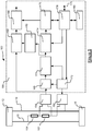
- FIG. 1 A block diagram representation of a first embodiment of electrical measurement apparatus is shown in Figure 1 .
- the electrical measurement apparatus has the form of current measurement apparatus 10 which forms part of the like of a 100A capable electricity consumption meter (not shown) installed at a point of supply to residential or business premises.
- a single phase mains alternating current electricity source 12 with live 14 and neutral 16 supply wires are shown in Figure 1 .
- Energy consuming apparatus at the residential or business premises is represented by a load 18.
- the current measurement apparatus 10 comprises a shunt resistor 20 (which constitutes a current sensor) in the live supply wire 14 in series with the load 18 between the load and the electricity supply 12.
- the shunt resistor 20 presents a low value of resistance, such as a resistance of 200u ⁇ .
- the shunt resistor 20 is formed from a length of electrical wire, a length of conductive track on a printed circuit board, a discrete component, a conductor comprised in an integrated circuit package such as a lead frame or a structure formed as part of a connector or conductive element of a series component such as a relay.
- the shunt resistor need not be formed to provide an accurate or stable resistance; nor need the processing chain for the shunt resistor be accurately characterised.
- a current transformer, a Hall current probe or a Rogowski coil current probe may be used to sense current in the live conductor instead of the shunt resistor 20.
- the use of such alternative forms of current sensor and appropriate processing circuitry is described in WO 2013/038176 .
- the current measurement apparatus 10 further comprises a signal source 22, voltage measuring apparatus 24 and signal processing circuitry 26.
- the voltage measuring apparatus 24 comprises programmable gain amplifier and analogue to digital conversion circuitry which is operative to acquire a voltage signal developed across the shunt resistor 20 and to generate a corresponding acquired voltage signal.
- the shunt resistor 20 and the voltage measuring apparatus 24 constitute a measurement arrangement and the signal processing circuitry 26 constitutes processing apparatus.
- the signal processing circuitry 26 is comprised in a microprocessor arrangement, digital signal processor arrangement or the like.
- the current measurement apparatus comprises a noise filter at the input of the voltage measuring apparatus 24 to suppress undesirable noise signals, such as impulse signals, which might otherwise be liable to disrupt operation of the current measurement apparatus.
- each of the voltage measuring apparatus 24 and the signal source 22 is electrically connected to opposite ends of the shunt resistor 20.
- the current measurement apparatus 10 is constituted such that the signal source 22 is always present with the rest of the current measurement apparatus 10 such that the signal source and the rest of the current measurement apparatus 10 is permanently in situ.
- the current measurement apparatus 10 is constituted such that the signal source is comprised in a separate unit from the rest of the current measurement apparatus 10, which is permanently in situ.
- the unit comprising the signal source 22 is brought into use, for example by a calibration engineer, and connected across the shunt resistor 20 before calibration begins. Approaches to calibration applicable to the current measurement apparatus of Figure 1 are described in WO 2013/038176 .
- the signal processing circuitry 26 comprises a windowing component 28, which is operative to apply a windowing function to the output signal from the voltage measuring apparatus 24.
- the windowing function applied by the windowing component 28 is one or more of a Hanning function, a Hamming function, a Blackman function, a Gaussian function and a rectangular function amongst others.
- the windowing function is either predetermined, such as on the basis of pre-characterisation of the measurement arrangement, or is determined on an ongoing basis, such as in dependence on analysis of the output signal from the voltage measuring apparatus 24.
- the window function is altered in dependence on an amplitude of the electrical output signal.
- the signal processing circuitry 26 also comprises a summing component 30 which is operative as described further below to sum sections of the output signal received from the windowing component 28.
- the operation of the signal source 22, the windowing component 28 and the summing component 30 is synchronised by way of timing signals generated by a timing component 32 comprised in the signal processing circuitry 26 as is described further below.
- the signal processing circuitry 26 further comprises a level determining component 34 which receives an output from the summing component 30 and a transfer function determining component 36 which receives an output from the level determining component 34.
- the signal processing circuitry 26 yet further comprises a control component 38, such as a central processing unit, which is operative to control various other components of the signal processing circuitry 26 including the timing component 32, the level determining component 34 and the transfer function determining component 36.
- the control component 38 also provides external data by way of a data output 39 in dependence on operation of the current measurement apparatus 10 with such external data including the like of alerts and control data which is acted upon by other apparatus.
- Electronic memory 40 comprised in signal processing circuitry 26 is operative to store intermediate data formed during computations performed by the signal processing circuitry 26 along with less impermanent data such as transfer function data of an historic nature determined by the signal processing circuitry.
- the electronic memory 40 is also operative to store data determined on initial test such as the value of the reference input signal, which is stored in a One Time Programmable form of memory.
- the signal processing circuitry 26 yet further comprises a waveform reconstruction component 42 which receives an output from the summing component 30, a waveform removal component 44 which receives an output from each of the waveform reconstruction component 42 and the voltage measuring apparatus 24, and a load current determining component 46 which receives an output from the waveform removal component 44.
- the source 12 is a DC source and the load 18 draws current from the DC source.
- Such embodiments are used in various applications, such as regulation or monitoring, and are comprised in diverse apparatus, such as energy generation, transmission or distribution apparatus, renewable energy generators, electrical propulsion apparatus and control apparatus.
- the current measurement apparatus is used for measuring current in multi-phase mains electricity supply arrangements such as a split-phase supply arrangement, a three phase supply arrangement or even a supply arrangement with more than three phases.
- plural current measurement apparatus of the form shown in Figure 1 are used to measure current in respective different conductors of the multi-phase mains electricity supply arrangement.
- DC current measurement is, for example, performed in electrical apparatus comprising an electric battery, such as propulsion apparatus.
- the signal source 22 is configured to apply a reference input signal to the shunt resistor 20 under the control of the timing component 32.
- the reference input signal has a repeating cycle in the range of a few hertz to a few tens of kHz.
- the reference input signal has a frequency largely between harmonics of the fundamental frequency of the load current signal. Alternatively the reference input signal frequency is locked to a harmonic of the fundamental frequency of the load current signal.
- the reference input signal is of substantially piecewise constant form such as a square wave, a bitstream having sections of highs and lows with different duty cycles, or a staircase or stepped waveform.
- a typical reference input signal is 30 mA peak to peak.
- the applied reference input signal is sensed by the shunt resistor 20 along with the load drawn current signal which in the present embodiment is a 50Hz mains current signal.
- the voltage measuring apparatus 24 is operative to acquire voltage signals developed across the shunt resistor 20 and to generate acquired voltage signals (which constitute output signals) 102.
- An acquired voltage signal comprises an electrical output signal corresponding to the load drawn current signal and a reference output signal corresponding to the reference input signal.
- the acquired voltage signal is received by the windowing component 28 which is operative to multiply the acquired voltage signal by the windowing function 104.
- the windowing function is of a length corresponding to plural cycles of the reference input signal, such as two hundred cycles.
- the windowing function is operative to attenuate the amplitude of part of the acquired voltage signal towards opposite ends of the window defined by the windowing function and thereby provide for improved rejection of the reference output signal during the subsequent summing operation.
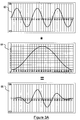
- Figure 3A shows a length of acquired voltage signal 62, a windowing function 64 and the length of acquired voltage signal after application of the windowing function 66.
- the application of the windowing function is liable to cause a loss in power from the output signal.
- loss of power is addressed by applying the windowing function to overlapping parts of the output signal.
- such overlapping streams of acquired voltage signal data are partially processed as described above with reference to one stream of data before being subsequently combined. For example the summing operation is performed separately on each stream and their levels determined separately. Alternatively the overlapping streams are processed together by summing the streams together.
- Application of the windowing function is under the control of the timing component 32 to provide for synchronisation of application of the windowing function to the acquired voltage signal with cycles of the reference input signal as applied by the signal source 22.
- the summing component 30 which is operative to decompose the length of voltage signal into plural portions with each portion corresponding to a cycle of the reference input signal.
- the voltage signal has a length of two hundred cycles the length of voltage signal is decomposed into two hundred portions.
- the summing component 30 then operative to sum sections of the two hundred portions, with each of the summed sections corresponding to at least a part and to a same part of the cycle of the reference input signal 106.
- the summing operation and the subsequent level determining operation within the level determining component 34 are carried in accordance with several different approaches.
- the entire portions of the voltage signal are summed to provide a cumulative representation. Summing the portions in this fashion removes the electrical output signal on account of the electrical output signal being of a different period to the reference output signal or of changing phase with respect to the reference output signal.
- the cumulative representation is then divided by the number of summed portions to provide a representation of amplitude commensurate with the reference input signal. Alternatively division by the number of summed portions takes place at a later step in the present approach.
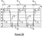
- a typical voltage signal comprises parts consisting of a slow rise or fall following each transition of the piecewise constant waveform followed perhaps by ringing.
- An example voltage signal of a length corresponding to several cycles 70 of the reference input signal is shown in Figure 3B .
- the voltage signal comprises rising parts 72, falling parts 74, high levels 76 and low levels 78.
- the summing component 30 is therefore operative to exclude such rising and falling parts and to select the generally settled parts of the voltage signal.
- the rising and falling parts are excluded following analysis of the voltage signal involving comparison of the rate of change of the voltage signal with a threshold value.
- rising and falling parts are excluded on the basis of pre-characterisation of the measurement arrangement which determines the rising and falling parts to be of a certain length following a transition in the reference input signal. Parts of corresponding level in the cumulative representation are then summed.
- the high levels are all summed and the low levels are all summed to provide a summed high level and a summed low level respectively.
- the summed high level and the summed low level are then divided by the number of summed levels to provide an average high level and an average low level.
- the division takes place later in the present approach. Irrespective of whether division is in the summing component or subsequently the effect is to provide an average level. Then the summed or average low is subtracted in the level determining component 34 from the summed or average high to provide a reference output signal amplitude 108.
- the summing component is operative to sum parts of corresponding level in the portions of the voltage signal to provide two cumulative representations.
- the summing component is operative to sum all the high levels in the portions to provide a summed high level and to sum all the low levels in the portions to provide a summed low level.
- the rising and falling parts are excluded from the summing operations as described above with reference to the first approach.
- the summed high and low levels are then divided by the number of summed levels to provide average levels. Alternatively the division takes place after the following subtraction step. Then the summed low level or average summed low level is subtracted in the level determining component 34 from the summed high level or average summed low level to provide a reference output signal amplitude 108.
- the summing component is operative to provide a reference output signal amplitude, which constitutes a cumulative representation, by summing the selected high levels and subtracting the selected low levels on an ongoing basis as the voltage signal is received 108.
- the operations of the summing component 30 and the level determining component 34 are thus combined.
- the reference output signal is divided by the number of summed levels. Alternatively the division takes place earlier in the approach, such as in respect of each level before it is either summed or subtracted.
- the reference output signal amplitude is received by the transfer function determining component 36 which is operative to determine a transfer function in respect of the gain of the measurement arrangement by dividing the reference output signal amplitude by the amplitude of the reference input signal 112.
- the transfer function determining component 36 is also operative to determine a group delay for the measurement arrangement by determining a time delay between an edge in the reference input signal and the corresponding edge in the reference output signal as represented by the acquired voltage signal 110. Where the windowing function causes loss of power from the reference output signal amplitude the transfer function determining component 36 is operative to compensate for such loss of power.
- the current measurement apparatus is operative such that the waveform reconstruction component 42 receives an input from the summing component 30.
- the waveform reconstruction component 42 is operative to provide a cumulative representation of a length of the voltage signal corresponding to a complete cycle of the reference input signal, i.e. a complete cumulative representation 114. Operation of the waveform reconstruction component 42 depends on operation of the summing component 30. Where the summing component 30 is operative according to the first approach the cumulative representation formed by summing entire portions of the voltage signal is already complete and is thus provided to the waveform reconstruction component 42 and no reconstruction is required.
- the waveform reconstruction component 42 is operative to form a complete cumulative representation from the different levels used to determine the reference output signal amplitude and the disregarded rising and falling parts.
- the complete cumulative representation is scaled to compensate for operations performed prior to formation of the complete cumulative representation, such as summing and windowing operations, whereby the complete cumulative representation corresponds to the acquired voltage signal from which it is subtracted in the waveform removal component 44 as described below.
- Figure 3C is a plot which illustrates operation of the waveform removal component 44.
- the waveform removal component 44 receives an input from the voltage measuring apparatus 24, 82 and the complete cumulative representation 84 from the waveform reconstruction component 42 and is operative to subtract the complete cumulative representation, which corresponds to the reference output signal, from the acquired voltage signal to leave the electrical output signal comprised in the acquired voltage signal 116, 86.
- the load current determining component 46 receives the output from the waveform removal component 44 and the transfer function from the transfer function determining component 36 and is operative to determine the load drawn current by applying the inverse of the received transfer function to the output from the waveform removal component 44, 118. The determined load drawn current is then provided by the load current determining component 46 for application elsewhere, such as in determination of power consumption or the like as described in detail in WO 2013/038176 .
- control component 38 provides for rejection of parts of the acquired voltage signal where such rejected parts comprise impulse noise of an extent that would prejudice proper operation of the current measurement apparatus.
- the control component 38 also provides for determination of the level of noise present in the acquired voltage signal by analysing the acquired voltage signal when no reference input signal is applied to the shunt resistor 20.
- the control component 38 is further operative to provide an indication of accuracy of current measurement in dependence on the determined level of noise.
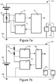
- FIG. 4 A block diagram representation of a second embodiment of the present invention 130 is shown in Figure 4 .
- Components of the current measurement apparatus 130 of Figure 4 in common with Figure 1 are designated with like reference numbers and the reader's attention is directed to the description provided above with reference to Figure 1 for a description of such common components.
- the current measurement apparatus 130 of Figure 4 further comprises a second shunt resistor 132 and a second voltage measuring apparatus 134. No reference input signal is applied to the second shunt resistor 132 whereby the output signal from second voltage measuring apparatus 134 comprises the electrical output signal but lacks the reference output signal.
- the current measurement apparatus 130 yet further comprises a subtraction component 136 which is operative to subtract the output signal from the second voltage measuring apparatus 134 from the output signal from the first voltage measuring apparatus 24.
- the subtraction component 136 also performs relative scaling of the received output signals to provide for proper subtraction of the output signals if required.
- the output from the subtraction component 136 has a much reduced component corresponding to the load drawn current signal.
- the waveform removal component 44 is operative on the output signal from the first voltage measuring apparatus 24 and not the output signal from the second voltage measuring apparatus 134.
- the configuration of Figure 4 may be used to effect when the applied reference input signal is much smaller than the load drawn current signal as is often the case. Subtraction of the electrical output signal according to the embodiment of Figure 4 is described in further detail in WO 2013/038176 in respect of different approaches to subtraction of the electrical output signal.
- FIG. 5 A block diagram representation of a third embodiment of electrical measurement apparatus is shown in Figure 5 .
- the electrical measurement apparatus has the form of voltage measurement apparatus 150 which is configured to measure the line voltage between the live and the neutral conductor of an AC system.
- the electrical measurement apparatus 150 forms part of the like of a 100A capable electricity consumption meter (not shown) installed at a point of supply to residential or business premises.
- a single phase mains alternating current electricity source 12 with live 14 and neutral 16 supply wires are shown in Figure 5 .
- Energy consuming apparatus at the residential or business premises is represented by a load 18.
- the electrical measurement apparatus 150 comprises a first resistor 154 in series with a second resistor 152 (which together constitute a potential attenuator) between the live conductor 14 the neutral conductor 16.
- the electrical measurement apparatus 150 further comprises a signal source 162 that is capable of providing a changing offset voltage to the potential attenuator; operation of the signal source 162 is described below.
- the first resistor 154 normally has a resistance value which is orders of magnitude larger than the resistance value of the second resistor 152 to thereby provide for measurement of line voltage of the order of 110V, 230V or the like.
- the first resistor 154 is constructed differently or out of several components in series to thereby manage its resistance value relative to the resistance value of the second resistor 152.
- the first and second resistors need not be chosen or constructed to provide an accurate or stable potential attenuator; nor need the processing chain for the potential attenuator be accurately characterised.
- Alternative forms of potential attenuator and signal source are described in WO 2014/072733 .
- the electrical measurement apparatus 150 of Figure 5 further comprises voltage measuring apparatus 164 and signal processing circuitry 166.
- the voltage measuring apparatus 164 comprises a programmable gain amplifier and analogue to digital conversion circuitry, which is operative to acquire a voltage signal developed across the second resistor 152 and to generate a corresponding acquired voltage signal.
- the signal processing circuitry 166 is comprised in a microprocessor arrangement, digital signal processor arrangement or the like.
- the electrical measurement apparatus 150 comprises a noise filter at the input of the voltage measuring apparatus 164 to suppress undesirable noise signals, such as impulse signals, which might otherwise be liable to disrupt operation of the electrical measurement apparatus.
- the signal source 162 is configured to generate an offset voltage.
- the signal source 162 generate an offset voltage by switching between different voltage levels or by other means of modulating between different voltage levels to generate a reference input signal in series with the potential attenuator. Approaches to calibration applicable to the electrical measurement apparatus of Figure 5 are described in WO 2014/072733 .
- the signal processing circuitry 166 comprises a windowing component 168 which is operative to apply a windowing function to the output signal from the voltage measuring apparatus 164.
- the windowing function applied by the windowing component 168 is one or more of a Hanning function, a Hamming function, a Blackman function, a Gaussian function and a rectangular function amongst others.
- the windowing function is either predetermined, such as on the basis of pre-characterisation of the measurement arrangement, or is determined on an ongoing basis, such as in dependence on analysis of the output signal from the voltage measuring apparatus 164.
- the windowing function is altered in dependence on an amplitude of the output signal from the voltage measuring apparatus 164.
- the signal processing circuitry 166 also comprises a summing component 170 which is operative as described further below to sum sections of the output signal received from the windowing component 168.
- the operation of the signal source 162, the windowing component 168 and the summing component 170 is synchronised by way of timing signals generated by a timing component 172 comprised in the signal processing circuitry 166 as is described further below.
- the signal processing circuitry 166 further comprises a level determining component 174 which receives an output from the summing component 170 and a transfer function determining component 176 which receives an output from the level determining component 174.
- the signal processing circuitry 166 yet further comprises a control component 178, such as a central processing unit, which is operative to control various other components of the signal processing circuitry 166 including the timing component 172, the level determining component 174 and the transfer function determining component 176.
- the control component 178 also provides external data by way of a data output 179 in dependence on operation of the electrical measurement apparatus 150 with such external data including the like of alerts and control data which is acted upon by other apparatus.
- Electronic memory 180 comprised in the signal processing circuitry 166 is operative to store intermediate data formed during computations performed by the signal processing circuitry 166 along with less impermanent data such as transfer function data of an historic nature determined by the signal processing circuitry.
- the electronic memory 180 is also operative to store data determined on initial test such as the value of the reference input signal, which is stored in a One Time Programmable form of memory.
- the signal processing circuitry 166 yet further comprises a waveform reconstruction component 182 which receives an output from the summing component 170, a waveform removal component 184 which receives an output from each of the waveform reconstruction component 182 and the voltage measuring apparatus 164, and a line voltage determining component 186 which receives an output from the waveform removal component 184.
- the source 12 is a DC source and the load 18 draws current from the DC source.
- the electrical measurement apparatus is used for measuring voltage in multi-phase mains electricity supply arrangements such as a split-phase supply arrangement, a three phase supply arrangement or even a supply arrangement with more than three phases.
- plural voltage measurement apparatus of the form shown in Figure 5 are used to measure voltage in respective different conductors of the multi-phase mains electricity supply arrangement.
- Application of electrical measurement apparatus to DC voltage measurement and in multi-phase mains electricity supply arrangements is described further in WO 2014/072733 .
- DC voltage measurement is, for example, performed in electrical apparatus comprising an electric battery, such as propulsion apparatus.
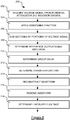
- the electrical measurement apparatus 150 of Figure 5 operates in a similar fashion to the current measurement apparatus of Figure 1 . Operational steps of the electrical measurement apparatus 150 of Figure 5 are represented in the flow chart 200 shown in Figure 6 . Operation of the electrical measurement apparatus 150 of Figure 5 will now be described.
- the signal source 162 is configured to apply a reference input signal to the potential attenuator 152, 154 under the control of the timing component 172.
- the reference input signal has a repeating cycle in the range of a few hertz to a few tens of kHz.
- the reference input signal has a frequency largely between harmonics of the fundamental frequency of the line voltage signal. Alternatively the reference input signal frequency is locked to a harmonic of the fundamental frequency of the line voltage signal.
- the reference input signal is of substantially piecewise constant form such as a square wave, a bitstream having sections of highs and lows with different duty cycles, a staircase waveform or a stepped waveform.
- a typical reference input signal is 200mV peak to peak.
- the applied reference input signal is sensed by the second resistor 152 along with the line voltage signal which in the present embodiment is a 50Hz mains voltage signal.
- the voltage measuring apparatus 164 is operative to acquire voltage signals developed across the reference resistor 152 and to generate acquired voltage signals (which constitute output signals) 202.
- An acquired voltage signal comprises an electrical output signal corresponding to the line voltage signal and a reference output signal corresponding to the reference input signal.
- the acquired voltage signal is received by the windowing component 168, which is operative to multiply the acquired voltage signal by the windowing function 204.
- the windowing function is of a length corresponding to plural cycles of the reference input signal, such as two hundred cycles.
- the windowing function is operative to attenuate the amplitude of part of the acquired voltage signal towards opposite ends of the window defined by the windowing function and thereby provide for improved rejection of the reference output signal during the subsequent summing operation.
- Figure 3A shows a length of acquired voltage signal 62, a windowing function 64 and the length of acquired voltage signal after application of the windowing function 66.
- the application of the windowing function is liable to cause a loss in power from the output signal.
- loss of power is addressed by applying the windowing function to overlapping parts of the output signal.
- such overlapping streams of acquired voltage signal data are partially processed as described above with reference to one stream of data before being subsequently combined. For example the summing operation is performed separately on each stream and their levels determined separately. Alternatively the overlapping streams are processed together by summing the streams together.
- Application of the windowing function is under the control of the timing component 172 to provide for synchronisation of application of the windowing function to the acquired voltage signal with cycles of the reference input signal as applied by the signal source 162.
- the summing component 170 which is operative to decompose the length of voltage signal into plural portions with each portion corresponding to a cycle of the reference input signal.
- the voltage signal has a length of two hundred cycles the length of voltage signal is decomposed into two hundred portions.
- the summing component 170 then operative to sum sections of the two hundred portions, with each of the summed sections corresponding to at least a part and to a same part of the cycle of the reference input signal 206.
- the summing operation and the subsequent level determining operation within the level determining component 174 are carried in accordance with several different approaches.
- the entire portions of the voltage signal are summed to provide a cumulative representation. Summing the portions in this fashion removes the electrical output signal on account of the electrical output signal being of a different period to the reference output signal or of changing phase with respect to the reference output signal.
- the cumulative representation is then divided by the number of summed portions to provide a representation of amplitude commensurate with the reference input signal. Alternatively division by the number of summed portions takes place at a later step in the present approach.
- a typical voltage signal comprises parts consisting of a slow rise or fall following each transition of the piecewise constant waveform followed perhaps by ringing.
- An example voltage signal of a length corresponding to several cycles 70 of the reference input signal is shown in Figure 3B .
- the voltage signal comprises rising parts 72, falling parts 74, high levels 76 and low levels 78.
- the summing component 170 is therefore operative to exclude such rising and falling parts and to select the generally settled parts of the voltage signal.
- the rising and falling parts are excluded following analysis of the voltage signal involving comparison of the rate of change of the voltage signal with a threshold value.
- rising and falling parts are excluded on the basis of pre-characterisation of the measurement arrangement which determines the rising and falling parts to be of a certain length following a transition in the reference input signal. Parts of corresponding level in the cumulative representation are then summed.
- the high levels are all summed and the low levels are all summed to provide a summed high level and a summed low level respectively.
- the summed high level and the summed low level are then divided by the number of summed levels to provide an average high level and an average low level.
- the division takes place later in the present approach. Irrespective of whether division is in the summing component or subsequently the effect is to provide an average level. Then the summed or average low is subtracted in the level determining component 174 from the summed or average high to provide a reference output signal amplitude 208.
- the summing component is operative to sum parts of corresponding level in the portions of the voltage signal to provide two cumulative representations.
- the summing component is operative to sum all the high levels in the portions to provide a summed high level and to sum all the low levels in the portions to provide a summed low level.
- the rising and falling parts are excluded from the summing operations as described above with reference to the first approach.
- the summed high and low levels are then divided by the number of summed levels to provide average levels. Alternatively the division takes place after the following subtraction step. Then the summed low level or average summed low level is subtracted in the level determining component 174 from the summed high level or average summed low level to provide a reference output signal amplitude 208.
- the summing component is operative to provide a reference output signal amplitude, which constitutes a cumulative representation, by summing the selected high levels and subtracting the selected low levels on an ongoing basis as the voltage signal is received 208.
- the operations of the summing component 170 and the level determining component 174 are thus combined.
- the reference output signal is divided by the number of summed levels. Alternatively the division takes place earlier in the approach, such as in respect of each level before it is either summed or subtracted.
- the reference output signal amplitude is received by the transfer function determining component 176 which is operative to determine a transfer function in respect of the gain of the measurement arrangement by dividing the reference output signal amplitude by the amplitude of the reference input signal 212.
- the transfer function determining component 176 is also operative to determine a group delay for the measurement arrangement by determining a time delay between an edge in the reference input signal and the corresponding edge in the reference output signal as represented by the acquired voltage signal 210. Where the windowing function causes loss of power from the reference output signal amplitude the transfer function determining component 176 is operative to compensate for such loss of power.
- the electrical measurement apparatus is operative such that the waveform reconstruction component 182 receives an input from the summing component 170.
- the waveform reconstruction component 172 is operative to provide a cumulative representation of a length of the voltage signal corresponding to a complete cycle of the reference input signal, i.e. a complete cumulative representation 214. Operation of the waveform reconstruction component 182 depends on operation of the summing component 170. Where the summing component 170 is operative according to the first approach the cumulative representation formed by summing entire portions of the voltage signal is already complete and is thus provided to the waveform reconstruction component 182 and no reconstruction is required.
- the waveform reconstruction component 182 is operative to form a complete cumulative representation from the different levels used to determine the reference output signal amplitude and the disregarded rising and falling parts.
- the complete cumulative representation is scaled to compensate for operations performed prior to formation of the complete cumulative representation, such as summing and windowing operations, whereby the complete cumulative representation corresponds to the acquired voltage signal from which it is subtracted in the waveform removal component 184 as described below.
- Figure 3C is a plot which illustrates operation of the waveform removal component 184.
- the waveform removal component 184 receives an input from the voltage measuring apparatus 164, 82 and the complete cumulative representation 84 from the waveform reconstruction component 182 and is operative to subtract the complete cumulative representation, which corresponds to the reference output signal, from the acquired voltage signal to leave the electrical output signal comprised in the acquired voltage signal 216, 86.
- the line voltage determining component 186 receives the output from the waveform removal component 184 and the transfer function from the transfer function determining component 176 and is operative to determine the line voltage by applying the inverse of the received transfer function to the output from the waveform removal component 184, 218. The determined line voltage is then provided by the line voltage determining component 186 for application elsewhere, such as in determination of power consumption or the like as described in detail in WO 2014/072733 .
- control component 178 provides for rejection of parts of the acquired voltage signal where such rejected parts comprise impulse noise of an extent that would prejudice proper operation of the electrical measurement apparatus.
- the control component 178 also provides for determination of the level of noise present in the acquired voltage signal by analysing the acquired voltage signal when no reference input signal is applied to the potential attenuator 154,152.
- the control component 178 is further operative to provide an indication of accuracy of voltage measurement in dependence on the determined level of noise.
- the present invention is applicable in DC apparatus.
- An example of such DC apparatus is propulsion apparatus comprising an electric battery.
- a block diagram representation of DC apparatus 300 in which electrical measurement apparatus embodying the present invention is used for low side current sensing is shown in Figure 7A .
- the DC apparatus 300 of Figure 7A is comprised in an electric vehicle or other battery powered device.
- the DC apparatus 300 comprises a battery 306.
- the delivered and charging current of the battery 306 is measured through a low-side sensor in the form of a shunt resistor 20.
- the DC apparatus 300 further comprises a signal source 22, voltage measuring apparatus 24 and processing apparatus 26 of a form and function as described above with reference to Figure 1 .
- the common node 308 between the battery 306 and a load 302 and a recharging circuit 310 is represented in Figure 7A as an effective ground point.
- the shunt resistor 20 When a load current is delivered by the battery 306 to the load 302, the shunt resistor 20 passes the same load current.
- the recharging circuit 310 e.g. a dynamo
- the battery charging current When the recharging circuit 310, e.g. a dynamo, recharges the battery 306 the current flowing into the shunt resistor 20 is the battery charging current.
- the shunt resistor 20 is therefore operative to measure current during discharging and charging of the battery.
- the load current changes significantly by orders of magnitude from mA's to 1000's Amps.
- the load current can have different frequency components depending on the nature of the load and on switching of the load.
- FIG. 7A A block diagram representation of DC apparatus 320 in which electrical measurement apparatus embodying the present invention is used for battery voltage measurement is shown in Figure 7A .
- the DC apparatus 320 of Figure 7B is comprised in an electric vehicle or other battery powered device.
- the DC apparatus 320 comprises a battery 306.
- the voltage of the battery 306 is measured through a potential divider 154, 152.
- the DC apparatus 300 further comprises a signal source 162, voltage measuring apparatus 164 and processing apparatus 166 of a form and function as described above with reference to Figure 5 .
- the common node 308 between the battery 306 and a load 302 and a recharging circuit 310 is represented in Figure 7B as an effective ground point.
- the battery 306 When a load current is delivered by the battery 306 to the load 302, or when the recharging circuit 310, e.g. a dynamo, recharges the battery 306 the potential divider 154, 152 attenuates the line voltage provided at the battery to a suitable level to be measured. In this way the battery can be monitored during different stages of discharging and charging.
- the battery voltage can change significantly from a few volts to 10's volts. Also the battery voltage can have different frequency components depending on the nature of the load and on switching of the load.
Claims (17)
- Appareil de mesure électrique (10) comprenant :- un dispositif de mesure (20) configuré pour être disposé en relation à un circuit électrique qui porte un signal électrique, le dispositif de mesure étant fonctionnel lorsqu'il est ainsi disposé pour mesurer le signal électrique ;- une source de signal (22) fonctionnelle pour appliquer un signal d'entrée de référence au dispositif de mesure (20) moyennant quoi un signal de sortie en provenance du dispositif de mesure comprend un signal de sortie électrique correspondant au signal électrique et un signal de sortie de référence correspondant au signal d'entrée de référence, le signal d'entrée de référence étant une onde carrée, une onde rectangulaire, un train de bits ayant des sections de hauts et de bas présentant des cycles de service différents, une forme d'onde en escalier ou une forme d'onde étagée et étant répété sur plusieurs cycles ; et- un appareil de traitement qui est fonctionnel pour déterminer au moins l'un parmi : une fonction de transfert pour le dispositif de mesure ; un changement d'une fonction de transfert pour le dispositif de mesure ; et le signal électrique, caractérisé en ce que l'appareil de traitement est en outre agencé pour déterminer au moins une représentation cumulée, la détermination de la représentation cumulée comprenant l'addition de plusieurs sections reçues du signal de sortie, chacune des plusieurs sections reçues correspondant à au moins une partie et à une même partie du cycle du signal d'entrée de référence ; et l'au moins une représentation cumulée et le signal d'entrée de référence sont utilisés pour déterminer l'au moins un de la fonction de transfert pour le dispositif de mesure, d'un changement de la fonction de transfert un dispositif de mesure et du signal électrique.
- Appareil de mesure électrique selon la revendication 1, dans lequel le circuit électrique porte un signal de courant, le dispositif de mesure comprend un capteur de courant qui est fonctionnel pour mesurer le signal de courant et la source de signal est configurée pour appliquer le signal d'entrée de référence en tant que courant.
- Appareil de mesure électrique selon l'une quelconque des revendications précédentes, dans lequel le circuit électrique porte un signal de tension, le dispositif de mesure comprend un atténuateur de potentiel qui est fonctionnel pour mesurer le signal de tension et la source de signal est configurée pour appliquer le signal d'entrée de référence sous la forme d'une tension.
- Appareil de mesure électrique selon l'une quelconque des revendications précédentes, dans lequel la détermination de la fonction de transfert comprend : la détermination d'au moins une amplitude cumulée en fonction de l'au moins une représentation cumulée ; et la détermination d'au moins une amplitude de signal de référence (108) par rapport au signal d'entrée de référence, la fonction de transfert étant déterminée en fonction de l'au moins une amplitude cumulée et de l'au moins une amplitude de signal de référence.
- Appareil de mesure électrique selon l'une quelconque des revendications précédentes, dans lequel l'appareil de traitement (26) est fonctionnel pour : additionner plusieurs différentes parties de l'au moins une représentation cumulée ; et diviser les plusieurs parties additionnées par le nombre de parties pour ainsi déterminer une représentation cumulée moyennée.
- Appareil de mesure électrique selon l'une quelconque des revendications précédentes, dans lequel l'appareil de traitement (26) est fonctionnel de manière à ce que la fonction de transfert soit déterminée par rapport à moins d'un cycle entier du signal d'entrée de référence et l'au moins une représentation cumulée correspond à moins d'un cycle entier du signal d'entrée de référence.
- Appareil de mesure électrique selon la revendication 6, dans lequel une représentation cumulée initiale est déterminée par addition de plusieurs sections reçues du signal de sortie et l'appareil de traitement est fonctionnel pour fournir des première et seconde représentations cumulées correspondant à différentes parties de la représentation cumulée initiale, les première et seconde représentations cumulées correspondant à moins que la représentation cumulée initiale totale ; ou dans lequel l'appareil de traitement est fonctionnel pour déterminer l'au moins une représentation cumulée en fonction de plusieurs sections reçues qui correspondent chacune à une partie du cycle du signal d'entrée de référence.
- Appareil de mesure électrique selon l'une quelconque des revendications 6 ou 7, dans lequel l'additionnement de plusieurs sections reçues du signal de sortie comprend l'addition de sous-sections correspondantes des plusieurs sections reçues, les sous-sections correspondantes étant sélectionnées en fonction d'au moins l'une de : la pré-caractérisation du comportement du dispositif de mesure ; et l'analyse du comportement du dispositif de mesure durant le fonctionnement de l'appareil de mesure électrique.
- Appareil de mesure électrique selon l'une quelconque des revendications précédentes, dans lequel l'appareil de traitement est fonctionnel pour déterminer la fonction de transfert par rapport à au moins une partie du cycle qui est identifiée comme ayant une variation relative à la transition, et dans lequel l'appareil de traitement est fonctionnel pour appliquer une pondération par rapport à une telle partie du cycle qui diffère de la pondération appliquée par rapport à une partie différente du cycle.
- Appareil de mesure électrique selon l'une quelconque des revendications précédentes, dans lequel au moins l'un des faits suivants s'applique :a) l'appareil de traitement est fonctionnel pour déterminer un retard d'au moins une transition du signal de sortie de référence par rapport à au moins une transition respective du signal d'entrée de référence, la fonction de transfert étant déterminée en fonction d'au moins un retard et au moins une amplitude cumulée pour ainsi fournir une fonction de transfert par rapport à la phase et à l'amplitude ;b) le dispositif de traitement est fonctionnel pour déterminer l'au moins une représentation cumulée sur une base continue dans lequel une première représentation cumulée est déterminée par addition d'une première pluralité de sections reçues et une seconde représentation cumulée est déterminée ensuite par addition d'une seconde pluralité de sections reçues, la seconde pluralité de sections reçues comprenant au moins une section reçue plus récemment absente de la première pluralité ;c) l'appareil de traitement est en outre fonctionnel sur des représentations cumulées sur une base sélective en fonction de la comparaison des représentations cumulées et de l'identification d'au moins une représentation cumulée qui s'écarte des autres représentations cumulées.
- Appareil de mesure électrique selon l'une quelconque des revendications précédentes, dans lequel l'appareil de traitement (26) est en outre fonctionnel pour appliquer une fonction de fenêtrage au signal de sortie, la fonction de fenêtrage étant appliquée avant la détermination de l'au moins une représentation cumulée, et la fonction de fenêtrage est configuré pour atténuer l'amplitude de la partie du signal de sortie vers des extrémités opposées de la fenêtre définie par la fonction de fenêtrage.
- Appareil de mesure électrique selon la revendication 11, dans lequel la détermination de la représentation cumulée comprend l'addition de correspondantes de plusieurs sections reçues du signal de sortie qui se chevauchent, la fonction de fenêtrage étant appliquée aux sections reçues qui se chevauchent.
- Appareil de mesure électrique selon l'une quelconque des revendications précédentes, dans lequel l'appareil de traitement est fonctionnel pour mettre à l'échelle la fonction de transfert pour ainsi compenser la mise à l'échelle causée par au moins l'un de : l'addition des plusieurs sections reçues du signal de sortie ; et, lorsqu'elle est dépendante de la revendication 11, l'application d'une fonction de fenêtrage au signal de sortie.
- Appareil de mesure électrique selon l'une quelconque des revendications précédentes, dans lequel l'appareil de traitement est fonctionnel pour transformer le signal de sortie reçu à partir de l'appareil de mesure avant la détermination de la représentation cumulée, et dans lequel le dispositif de mesure est configuré pour effectuer une nouvelle mesure du signal électrique, aucun signal d'entrée de référence n'étant appliqué durant la nouvelle mesure et la transformation du signal de sortie comprend la soustraction de la nouvelle mesure du signal électrique du signal de sortie reçu à partir de l'appareil de mesure.
- Appareil de mesure électrique selon l'une quelconque des revendications précédentes, dans lequel l'appareil de traitement est en outre fonctionnel pour soustraire l'au moins une représentation cumulée du signal de sortie pour ainsi retirer le signal de sortie de référence du signal de sortie.
- Appareil électrique comprenant un appareil de mesure électrique selon l'une quelconque des revendications précédentes, l'appareil électrique étant configuré de telle manière que l'appareil de mesure électrique mesure un signal électrique porté par l'appareil électrique, dans lequel l'appareil de mesure électrique est configuré pour mesurer au moins l'un parmi : un courant approvisionné par l'appareil CC ; un courant absorbé par l'appareil CC ; et une tension entre deux conducteurs dans l'appareil CC, ou l'appareil de mesure électrique est configuré pour mesurer au moins l'un parmi : un courant approvisionné par l'appareil CA ; un courant absorbé par l'appareil CA ; et une tension entre deux conducteurs dans l'appareil CA.
- Procédé de mesure électrique comprenant :- l'application d'un signal d'entrée de référence au moyen d'une source de signal à un dispositif de mesure disposé en relation à un circuit électrique qui porte un courant électrique et/ou un signal de tension, le dispositif de mesure étant fonctionnel lorsqu'il est ainsi disposé pour mesurer le signal électrique ;- la réception d'un signal de sortie en provenance du dispositif de mesure dans l'appareil de traitement, le signal de sortie comprenant un signal de sortie électrique correspondant au signal électrique et un signal de sortie de référence correspondant au signal d'entrée de référence, le signal d'entrée de référence qui est répété sur chacun de plusieurs cycles, et sous la forme d'une onde carrée, d'une onde rectangulaire, d'un train de bits ayant des sections de hauts et de bas présentant des cycles de service différents, d'une forme d'onde en escalier ou d'une forme d'onde étagée ;- la détermination d'au moins une représentation cumulée, la détermination de la représentation cumulée comprenant l'addition de plusieurs sections reçues du signal de sortie, chacune des plusieurs sections reçues correspondant à au moins une partie et à une même partie du cycle du signal d'entrée de référence ; et- la détermination d'au moins l'un parmi : une fonction de transfert pour le dispositif de mesure ; un changement d'une fonction de transfert pour le dispositif de mesure ; et le signal électrique, ladite détermination basée sur l'au moins une représentation cumulée et le signal d'entrée de référence.
Applications Claiming Priority (2)
| Application Number | Priority Date | Filing Date | Title |
|---|---|---|---|
| GBGB1309823.1A GB201309823D0 (en) | 2013-06-01 | 2013-06-01 | Current measurement |
| PCT/GB2014/051676 WO2014191776A1 (fr) | 2013-06-01 | 2014-05-30 | Mesure de signal électrique |
Publications (2)
| Publication Number | Publication Date |
|---|---|
| EP3004901A1 EP3004901A1 (fr) | 2016-04-13 |
| EP3004901B1 true EP3004901B1 (fr) | 2019-07-03 |
Family
ID=48805615
Family Applications (1)
| Application Number | Title | Priority Date | Filing Date |
|---|---|---|---|
| EP14734206.7A Active EP3004901B1 (fr) | 2013-06-01 | 2014-05-30 | Mesure de signal électrique |
Country Status (6)
| Country | Link |
|---|---|
| US (1) | US9823275B2 (fr) |
| EP (1) | EP3004901B1 (fr) |
| JP (1) | JP6407978B2 (fr) |
| CN (2) | CN109239435B (fr) |
| GB (1) | GB201309823D0 (fr) |
| WO (1) | WO2014191776A1 (fr) |
Families Citing this family (16)
| Publication number | Priority date | Publication date | Assignee | Title |
|---|---|---|---|---|
| GB201309825D0 (en) * | 2013-06-01 | 2013-07-17 | Metroic Ltd | Current measurement |
| GB201309823D0 (en) * | 2013-06-01 | 2013-07-17 | Metroic Ltd | Current measurement |
| CN105807128B (zh) * | 2016-03-16 | 2018-09-28 | 中国计量科学研究院 | 将多周期策略用于数模转换测量交流电压的方法及系统 |
| US10459013B2 (en) * | 2016-06-17 | 2019-10-29 | Analog Devices Global | Apparatus for and method of providing measurements of uncertainty in respect of a transfer function |
| US10768262B2 (en) * | 2017-08-30 | 2020-09-08 | Analog Devices Global Unlimited Campany | Managing the determination of a transfer function of a measurement sensor |
| US11067604B2 (en) * | 2017-08-30 | 2021-07-20 | Analog Devices International Unlimited Company | Managing the determination of a transfer function of a measurement sensor |
| US10914808B2 (en) * | 2017-08-30 | 2021-02-09 | Analog Devices International Unlimited Company | Managing the determination of a transfer function of a measurement sensor |
| GB201801910D0 (en) | 2018-02-06 | 2018-03-21 | Analog Devices Global Unlimited Co | A non-contacting voltage measuring apparatus |
| US10845393B2 (en) * | 2017-09-11 | 2020-11-24 | Analog Devices International Limited Company | Current measurement |
| WO2020056754A1 (fr) | 2018-09-21 | 2020-03-26 | Analog Devices Global Unlimited Company | Appareil et procédé permettant de supprimer un signal de perturbation d'un flux de données en série, et appareil de mesure et/ou de protection comprenant un tel appareil de suppression de signal |
| US11092623B2 (en) * | 2018-12-11 | 2021-08-17 | Electronics And Telecommunications Research Institute | Current sensor for measuring alternating electromagnetic wave and a current breaker using the same |
| US11239872B2 (en) * | 2020-05-21 | 2022-02-01 | SK Hynix Inc. | Signal receiver and method of measuring offset of signal receiver |
| US11435404B2 (en) | 2020-09-28 | 2022-09-06 | Analog Devices International Unlimited Company | Battery formation/testing |
| US11686747B2 (en) | 2020-09-28 | 2023-06-27 | Analog Devices International Unlimited Company | DC signal measurement and battery formation/testing |
| US11892433B2 (en) * | 2021-08-02 | 2024-02-06 | Thermo Finnigan Llc | Electrospray current measurement in the nanospray and microspray regime |
| CN114567385B (zh) * | 2022-01-12 | 2023-05-09 | 中国电子科技集团公司第十研究所 | 一体化大功率信号源 |
Family Cites Families (26)
| Publication number | Priority date | Publication date | Assignee | Title |
|---|---|---|---|---|
| GB2089153B (en) * | 1980-12-04 | 1984-05-23 | Yamato Scale Co Ltd | Combination weighing machine |
| US4423458A (en) | 1982-04-05 | 1983-12-27 | Siemens-Allis, Inc. | Signal processing system for overload relay or the like |
| EP0427953B1 (fr) * | 1989-10-06 | 1996-01-17 | Matsushita Electric Industrial Co., Ltd. | Appareil et méthode pour la modification du débit de parole |
| US5386188A (en) * | 1993-01-15 | 1995-01-31 | Keithley Instruments, Inc. | In-circuit current measurement |
| US5673196A (en) | 1995-11-30 | 1997-09-30 | General Electric Company | Vector electricity meters and associated vector electricity metering methods |
| US5804979A (en) | 1997-05-13 | 1998-09-08 | Fluke Corporation | Circuit for measuring in-circuit resistance and current |
| ES2281120T3 (es) * | 1998-12-08 | 2007-09-16 | Irdeto Access B.V. | Sistema para el proceso de una señal de informacion. |
| JP4222678B2 (ja) * | 1999-04-09 | 2009-02-12 | 横河電機株式会社 | 電流測定装置 |
| JP3415579B2 (ja) * | 2000-11-09 | 2003-06-09 | 松下電器産業株式会社 | マッチドフィルタおよび相関検出演算方法 |
| AT414048B (de) | 2004-07-06 | 2006-08-15 | Lem Norma Gmbh | Verfahren und einrichtung zur strommessung |
| EP1637898A1 (fr) * | 2004-09-16 | 2006-03-22 | Liaisons Electroniques-Mecaniques Lem S.A. | Capteur de champs magnétique à calibration continue |
| EP2017868B1 (fr) | 2005-08-02 | 2014-10-22 | Phoenix Contact GmbH & Co. KG | Etage de sortie de puissance triphasée |
| US8008948B2 (en) * | 2006-07-06 | 2011-08-30 | Denso Corporation | Peak voltage detector circuit and binarizing circuit including the same circuit |
| EP1936393A1 (fr) | 2006-12-22 | 2008-06-25 | Abb Research Ltd. | Appareil et procédé de mesure d'impédance |
| JP4955485B2 (ja) * | 2007-08-28 | 2012-06-20 | ルネサスエレクトロニクス株式会社 | 水平同期検出装置 |
| EP2261681A4 (fr) * | 2008-04-04 | 2014-11-05 | Anritsu Corp | Procédé de détection de composante de battement d'onde fondamentale, dispositif d'échantillonnage pour signal mesuré à l'aide de celui-ci, et système d'observation de forme d'ondes |
| CN101881791B (zh) * | 2009-04-30 | 2015-08-05 | 日置电机株式会社 | 电压检测装置 |
| CN101789687B (zh) * | 2010-03-23 | 2012-01-25 | 浙江大学 | 基于电感电流自校准无损检测的平均电流模式控制器 |
| CN101799485B (zh) * | 2010-04-12 | 2011-11-23 | 哈尔滨工业大学 | 岩心夹持器、采用该岩心夹持器的岩心zeta电势测量系统及测量方法 |
| CN102095915B (zh) * | 2010-11-24 | 2013-04-17 | 重庆大学 | 一种采用多同步参考坐标系变换的电压信号检测装置 |
| CN102645574B (zh) * | 2011-02-21 | 2015-06-10 | 华东电力试验研究院有限公司 | 基于网络传递函数计算的现场暂态过电压测量方法 |
| US9151818B2 (en) | 2011-11-08 | 2015-10-06 | Analog Devices Global | Voltage measurement |
| EP2756318A2 (fr) * | 2011-09-12 | 2014-07-23 | Metroic Limited | Mesure du courant |
| CN102565523B (zh) * | 2012-01-12 | 2014-12-17 | 上海理工大学 | 一种电流谐波检测系统及工作方法 |
| US9404948B2 (en) * | 2012-12-21 | 2016-08-02 | Microchip Technology Incorporated | Mains voltage zero-crossing detector |
| GB201309823D0 (en) * | 2013-06-01 | 2013-07-17 | Metroic Ltd | Current measurement |
-
2013
- 2013-06-01 GB GBGB1309823.1A patent/GB201309823D0/en not_active Ceased
-
2014
- 2014-05-30 EP EP14734206.7A patent/EP3004901B1/fr active Active
- 2014-05-30 CN CN201810953719.5A patent/CN109239435B/zh active Active
- 2014-05-30 CN CN201480030949.4A patent/CN105247376B/zh active Active
- 2014-05-30 WO PCT/GB2014/051676 patent/WO2014191776A1/fr active Application Filing
- 2014-05-30 JP JP2016516251A patent/JP6407978B2/ja active Active
- 2014-05-30 US US14/895,868 patent/US9823275B2/en active Active
Non-Patent Citations (1)
| Title |
|---|
| None * |
Also Published As
| Publication number | Publication date |
|---|---|
| GB201309823D0 (en) | 2013-07-17 |
| CN105247376B (zh) | 2018-09-04 |
| CN109239435B (zh) | 2022-05-27 |
| CN105247376A (zh) | 2016-01-13 |
| EP3004901A1 (fr) | 2016-04-13 |
| US20160154029A1 (en) | 2016-06-02 |
| US9823275B2 (en) | 2017-11-21 |
| JP6407978B2 (ja) | 2018-10-17 |
| WO2014191776A1 (fr) | 2014-12-04 |
| CN109239435A (zh) | 2019-01-18 |
| JP2016520203A (ja) | 2016-07-11 |
Similar Documents
| Publication | Publication Date | Title |
|---|---|---|
| EP3004901B1 (fr) | Mesure de signal électrique | |
| US11016126B2 (en) | Current measurement | |
| US10527651B2 (en) | Current measurement | |
| CN108802462B (zh) | 电压测量 | |
| JP7412386B2 (ja) | 電流変換器内の位相誤差又はタイミング遅延を学習するための方法および装置並びに電流変換器の誤差訂正を含む電力測定装置 | |
| JP3312167B2 (ja) | 電気エネルギ消費量をデジタル的に測定するための方法および装置 | |
| US20190079117A1 (en) | Current Measurement | |
| EP1777530A1 (fr) | Procédé et appareil pour mesurer des courants de sortie dans des circuits onduleurs | |
| Bucci et al. | Embedded power and energy measurement system based on an analog multiplier | |
| Wang et al. | Harmonic impedance measurement using a thyristor-controlled short circuit | |
| RU2554308C1 (ru) | Устройство для измерения сопротивления изоляции сетей переменного тока | |
| Do Thanh et al. | Nonsinusoidal power caused by measurements of grid impedances at unbalanced grid voltages | |
| US11360129B2 (en) | Measurement apparatus and method | |
| RU2363960C1 (ru) | Способ измерения сопротивления изоляции присоединений в разветвленных сетях постоянного тока |
Legal Events
| Date | Code | Title | Description |
|---|---|---|---|
| PUAI | Public reference made under article 153(3) epc to a published international application that has entered the european phase |
Free format text: ORIGINAL CODE: 0009012 |
|
| 17P | Request for examination filed |
Effective date: 20151209 |
|
| AK | Designated contracting states |
Kind code of ref document: A1 Designated state(s): AL AT BE BG CH CY CZ DE DK EE ES FI FR GB GR HR HU IE IS IT LI LT LU LV MC MK MT NL NO PL PT RO RS SE SI SK SM TR |
|
| AX | Request for extension of the european patent |
Extension state: BA ME |
|
| DAX | Request for extension of the european patent (deleted) | ||
| RAP1 | Party data changed (applicant data changed or rights of an application transferred) |
Owner name: ANALOG DEVICES GLOBAL UNLIMITED COMPANY |
|
| GRAP | Despatch of communication of intention to grant a patent |
Free format text: ORIGINAL CODE: EPIDOSNIGR1 |
|
| STAA | Information on the status of an ep patent application or granted ep patent |
Free format text: STATUS: GRANT OF PATENT IS INTENDED |
|
| RIC1 | Information provided on ipc code assigned before grant |
Ipc: G01R 19/25 20060101ALI20181130BHEP Ipc: G01R 19/165 20060101ALI20181130BHEP Ipc: G01R 21/133 20060101AFI20181130BHEP Ipc: G01R 27/08 20060101ALI20181130BHEP Ipc: G01R 11/66 20060101ALI20181130BHEP Ipc: G01R 1/20 20060101ALI20181130BHEP Ipc: G01R 15/14 20060101ALI20181130BHEP Ipc: G01R 17/02 20060101ALI20181130BHEP Ipc: G01R 17/00 20060101ALI20181130BHEP Ipc: G01R 11/25 20060101ALI20181130BHEP Ipc: G01R 19/00 20060101ALI20181130BHEP Ipc: G01R 27/14 20060101ALI20181130BHEP |
|
| INTG | Intention to grant announced |
Effective date: 20181217 |
|
| GRAS | Grant fee paid |
Free format text: ORIGINAL CODE: EPIDOSNIGR3 |
|
| GRAA | (expected) grant |
Free format text: ORIGINAL CODE: 0009210 |
|
| STAA | Information on the status of an ep patent application or granted ep patent |
Free format text: STATUS: THE PATENT HAS BEEN GRANTED |
|
| AK | Designated contracting states |
Kind code of ref document: B1 Designated state(s): AL AT BE BG CH CY CZ DE DK EE ES FI FR GB GR HR HU IE IS IT LI LT LU LV MC MK MT NL NO PL PT RO RS SE SI SK SM TR |
|
| REG | Reference to a national code |
Ref country code: GB Ref legal event code: FG4D |
|
| REG | Reference to a national code |
Ref country code: CH Ref legal event code: EP Ref country code: AT Ref legal event code: REF Ref document number: 1151650 Country of ref document: AT Kind code of ref document: T Effective date: 20190715 |
|
| REG | Reference to a national code |
Ref country code: IE Ref legal event code: FG4D |
|
| REG | Reference to a national code |
Ref country code: DE Ref legal event code: R096 Ref document number: 602014049466 Country of ref document: DE |
|
| REG | Reference to a national code |
Ref country code: NL Ref legal event code: MP Effective date: 20190703 |
|
| REG | Reference to a national code |
Ref country code: LT Ref legal event code: MG4D |
|
| REG | Reference to a national code |
Ref country code: AT Ref legal event code: MK05 Ref document number: 1151650 Country of ref document: AT Kind code of ref document: T Effective date: 20190703 |
|
| PG25 | Lapsed in a contracting state [announced via postgrant information from national office to epo] |
Ref country code: SE Free format text: LAPSE BECAUSE OF FAILURE TO SUBMIT A TRANSLATION OF THE DESCRIPTION OR TO PAY THE FEE WITHIN THE PRESCRIBED TIME-LIMIT Effective date: 20190703 Ref country code: NL Free format text: LAPSE BECAUSE OF FAILURE TO SUBMIT A TRANSLATION OF THE DESCRIPTION OR TO PAY THE FEE WITHIN THE PRESCRIBED TIME-LIMIT Effective date: 20190703 Ref country code: BG Free format text: LAPSE BECAUSE OF FAILURE TO SUBMIT A TRANSLATION OF THE DESCRIPTION OR TO PAY THE FEE WITHIN THE PRESCRIBED TIME-LIMIT Effective date: 20191003 Ref country code: AT Free format text: LAPSE BECAUSE OF FAILURE TO SUBMIT A TRANSLATION OF THE DESCRIPTION OR TO PAY THE FEE WITHIN THE PRESCRIBED TIME-LIMIT Effective date: 20190703 Ref country code: HR Free format text: LAPSE BECAUSE OF FAILURE TO SUBMIT A TRANSLATION OF THE DESCRIPTION OR TO PAY THE FEE WITHIN THE PRESCRIBED TIME-LIMIT Effective date: 20190703 Ref country code: NO Free format text: LAPSE BECAUSE OF FAILURE TO SUBMIT A TRANSLATION OF THE DESCRIPTION OR TO PAY THE FEE WITHIN THE PRESCRIBED TIME-LIMIT Effective date: 20191003 Ref country code: LT Free format text: LAPSE BECAUSE OF FAILURE TO SUBMIT A TRANSLATION OF THE DESCRIPTION OR TO PAY THE FEE WITHIN THE PRESCRIBED TIME-LIMIT Effective date: 20190703 Ref country code: PT Free format text: LAPSE BECAUSE OF FAILURE TO SUBMIT A TRANSLATION OF THE DESCRIPTION OR TO PAY THE FEE WITHIN THE PRESCRIBED TIME-LIMIT Effective date: 20191104 Ref country code: CZ Free format text: LAPSE BECAUSE OF FAILURE TO SUBMIT A TRANSLATION OF THE DESCRIPTION OR TO PAY THE FEE WITHIN THE PRESCRIBED TIME-LIMIT Effective date: 20190703 Ref country code: FI Free format text: LAPSE BECAUSE OF FAILURE TO SUBMIT A TRANSLATION OF THE DESCRIPTION OR TO PAY THE FEE WITHIN THE PRESCRIBED TIME-LIMIT Effective date: 20190703 |
|
| PG25 | Lapsed in a contracting state [announced via postgrant information from national office to epo] |
Ref country code: LV Free format text: LAPSE BECAUSE OF FAILURE TO SUBMIT A TRANSLATION OF THE DESCRIPTION OR TO PAY THE FEE WITHIN THE PRESCRIBED TIME-LIMIT Effective date: 20190703 Ref country code: GR Free format text: LAPSE BECAUSE OF FAILURE TO SUBMIT A TRANSLATION OF THE DESCRIPTION OR TO PAY THE FEE WITHIN THE PRESCRIBED TIME-LIMIT Effective date: 20191004 Ref country code: ES Free format text: LAPSE BECAUSE OF FAILURE TO SUBMIT A TRANSLATION OF THE DESCRIPTION OR TO PAY THE FEE WITHIN THE PRESCRIBED TIME-LIMIT Effective date: 20190703 Ref country code: AL Free format text: LAPSE BECAUSE OF FAILURE TO SUBMIT A TRANSLATION OF THE DESCRIPTION OR TO PAY THE FEE WITHIN THE PRESCRIBED TIME-LIMIT Effective date: 20190703 Ref country code: RS Free format text: LAPSE BECAUSE OF FAILURE TO SUBMIT A TRANSLATION OF THE DESCRIPTION OR TO PAY THE FEE WITHIN THE PRESCRIBED TIME-LIMIT Effective date: 20190703 Ref country code: IS Free format text: LAPSE BECAUSE OF FAILURE TO SUBMIT A TRANSLATION OF THE DESCRIPTION OR TO PAY THE FEE WITHIN THE PRESCRIBED TIME-LIMIT Effective date: 20191103 |
|
| PG25 | Lapsed in a contracting state [announced via postgrant information from national office to epo] |
Ref country code: TR Free format text: LAPSE BECAUSE OF FAILURE TO SUBMIT A TRANSLATION OF THE DESCRIPTION OR TO PAY THE FEE WITHIN THE PRESCRIBED TIME-LIMIT Effective date: 20190703 |
|
| PG25 | Lapsed in a contracting state [announced via postgrant information from national office to epo] |
Ref country code: DK Free format text: LAPSE BECAUSE OF FAILURE TO SUBMIT A TRANSLATION OF THE DESCRIPTION OR TO PAY THE FEE WITHIN THE PRESCRIBED TIME-LIMIT Effective date: 20190703 Ref country code: RO Free format text: LAPSE BECAUSE OF FAILURE TO SUBMIT A TRANSLATION OF THE DESCRIPTION OR TO PAY THE FEE WITHIN THE PRESCRIBED TIME-LIMIT Effective date: 20190703 Ref country code: EE Free format text: LAPSE BECAUSE OF FAILURE TO SUBMIT A TRANSLATION OF THE DESCRIPTION OR TO PAY THE FEE WITHIN THE PRESCRIBED TIME-LIMIT Effective date: 20190703 Ref country code: PL Free format text: LAPSE BECAUSE OF FAILURE TO SUBMIT A TRANSLATION OF THE DESCRIPTION OR TO PAY THE FEE WITHIN THE PRESCRIBED TIME-LIMIT Effective date: 20190703 |
|
| PG25 | Lapsed in a contracting state [announced via postgrant information from national office to epo] |
Ref country code: SK Free format text: LAPSE BECAUSE OF FAILURE TO SUBMIT A TRANSLATION OF THE DESCRIPTION OR TO PAY THE FEE WITHIN THE PRESCRIBED TIME-LIMIT Effective date: 20190703 Ref country code: IS Free format text: LAPSE BECAUSE OF FAILURE TO SUBMIT A TRANSLATION OF THE DESCRIPTION OR TO PAY THE FEE WITHIN THE PRESCRIBED TIME-LIMIT Effective date: 20200224 Ref country code: SM Free format text: LAPSE BECAUSE OF FAILURE TO SUBMIT A TRANSLATION OF THE DESCRIPTION OR TO PAY THE FEE WITHIN THE PRESCRIBED TIME-LIMIT Effective date: 20190703 |
|
| REG | Reference to a national code |
Ref country code: DE Ref legal event code: R097 Ref document number: 602014049466 Country of ref document: DE |
|
| PLBE | No opposition filed within time limit |
Free format text: ORIGINAL CODE: 0009261 |
|
| STAA | Information on the status of an ep patent application or granted ep patent |
Free format text: STATUS: NO OPPOSITION FILED WITHIN TIME LIMIT |
|
| PG2D | Information on lapse in contracting state deleted |
Ref country code: IS |
|
| 26N | No opposition filed |
Effective date: 20200603 |
|
| PG25 | Lapsed in a contracting state [announced via postgrant information from national office to epo] |
Ref country code: SI Free format text: LAPSE BECAUSE OF FAILURE TO SUBMIT A TRANSLATION OF THE DESCRIPTION OR TO PAY THE FEE WITHIN THE PRESCRIBED TIME-LIMIT Effective date: 20190703 |
|
| PG25 | Lapsed in a contracting state [announced via postgrant information from national office to epo] |
Ref country code: CH Free format text: LAPSE BECAUSE OF NON-PAYMENT OF DUE FEES Effective date: 20200531 Ref country code: LI Free format text: LAPSE BECAUSE OF NON-PAYMENT OF DUE FEES Effective date: 20200531 Ref country code: MC Free format text: LAPSE BECAUSE OF FAILURE TO SUBMIT A TRANSLATION OF THE DESCRIPTION OR TO PAY THE FEE WITHIN THE PRESCRIBED TIME-LIMIT Effective date: 20190703 |
|
| REG | Reference to a national code |
Ref country code: BE Ref legal event code: MM Effective date: 20200531 |
|
| PG25 | Lapsed in a contracting state [announced via postgrant information from national office to epo] |
Ref country code: LU Free format text: LAPSE BECAUSE OF NON-PAYMENT OF DUE FEES Effective date: 20200530 |
|
| PG25 | Lapsed in a contracting state [announced via postgrant information from national office to epo] |
Ref country code: IE Free format text: LAPSE BECAUSE OF NON-PAYMENT OF DUE FEES Effective date: 20200530 |
|
| PG25 | Lapsed in a contracting state [announced via postgrant information from national office to epo] |
Ref country code: BE Free format text: LAPSE BECAUSE OF NON-PAYMENT OF DUE FEES Effective date: 20200531 |
|
| PGFP | Annual fee paid to national office [announced via postgrant information from national office to epo] |
Ref country code: IT Payment date: 20210422 Year of fee payment: 8 |
|
| REG | Reference to a national code |
Ref country code: GB Ref legal event code: 732E Free format text: REGISTERED BETWEEN 20211014 AND 20211020 |
|
| PG25 | Lapsed in a contracting state [announced via postgrant information from national office to epo] |
Ref country code: MT Free format text: LAPSE BECAUSE OF FAILURE TO SUBMIT A TRANSLATION OF THE DESCRIPTION OR TO PAY THE FEE WITHIN THE PRESCRIBED TIME-LIMIT Effective date: 20190703 Ref country code: CY Free format text: LAPSE BECAUSE OF FAILURE TO SUBMIT A TRANSLATION OF THE DESCRIPTION OR TO PAY THE FEE WITHIN THE PRESCRIBED TIME-LIMIT Effective date: 20190703 |
|
| PG25 | Lapsed in a contracting state [announced via postgrant information from national office to epo] |
Ref country code: MK Free format text: LAPSE BECAUSE OF FAILURE TO SUBMIT A TRANSLATION OF THE DESCRIPTION OR TO PAY THE FEE WITHIN THE PRESCRIBED TIME-LIMIT Effective date: 20190703 |
|
| REG | Reference to a national code |
Ref country code: DE Ref legal event code: R081 Ref document number: 602014049466 Country of ref document: DE Owner name: ANALOG DEVICES INTERNATIONAL UNLIMITED COMPANY, IE Free format text: FORMER OWNER: ANALOG DEVICES GLOBAL UNLIMITED COMPANY, HAMILTON, BM |
|
| PG25 | Lapsed in a contracting state [announced via postgrant information from national office to epo] |
Ref country code: IT Free format text: LAPSE BECAUSE OF NON-PAYMENT OF DUE FEES Effective date: 20220530 |
|
| PGFP | Annual fee paid to national office [announced via postgrant information from national office to epo] |
Ref country code: FR Payment date: 20230420 Year of fee payment: 10 Ref country code: DE Payment date: 20230419 Year of fee payment: 10 |
|
| PGFP | Annual fee paid to national office [announced via postgrant information from national office to epo] |
Ref country code: GB Payment date: 20230420 Year of fee payment: 10 |