EP3002877B1 - Integrierte Schaltvorrichtung mit eingebetteter programmierbarer Logik - Google Patents
Integrierte Schaltvorrichtung mit eingebetteter programmierbarer Logik Download PDFInfo
- Publication number
- EP3002877B1 EP3002877B1 EP14187541.9A EP14187541A EP3002877B1 EP 3002877 B1 EP3002877 B1 EP 3002877B1 EP 14187541 A EP14187541 A EP 14187541A EP 3002877 B1 EP3002877 B1 EP 3002877B1
- Authority
- EP
- European Patent Office
- Prior art keywords
- integrated circuit
- programmable logic
- memory
- configuration
- memory module
- Prior art date
- Legal status (The legal status is an assumption and is not a legal conclusion. Google has not performed a legal analysis and makes no representation as to the accuracy of the status listed.)
- Active
Links
Images



Classifications
-
- H—ELECTRICITY
- H03—ELECTRONIC CIRCUITRY
- H03K—PULSE TECHNIQUE
- H03K19/00—Logic circuits, i.e. having at least two inputs acting on one output; Inverting circuits
- H03K19/02—Logic circuits, i.e. having at least two inputs acting on one output; Inverting circuits using specified components
- H03K19/173—Logic circuits, i.e. having at least two inputs acting on one output; Inverting circuits using specified components using elementary logic circuits as components
- H03K19/177—Logic circuits, i.e. having at least two inputs acting on one output; Inverting circuits using specified components using elementary logic circuits as components arranged in matrix form
- H03K19/1778—Structural details for adapting physical parameters
- H03K19/17796—Structural details for adapting physical parameters for physical disposition of blocks
Definitions
- This disclosure relates to integrated circuit devices and, more particularly, integrated circuit devices configured through programmable logic embedded within the integrated circuit devices.
- Integrated circuits are found in a variety of electronic systems. Computers, handheld devices, portable phones, televisions, industrial control systems, and robotics, to name just a few, rely on integrated circuits.
- a first integrated circuit such as a field programmable gate array (FPGA)
- FPGA field programmable gate array
- memory such as memory
- ASIC application-specific integrated circuit
- an industry standard such as standards for chip-to-chip interfaces
- this may include changing from a first universal interface block (UIB 1) to a second universal interface block (UIB2).
- UOB 1 first universal interface block
- UB2 second universal interface block
- an integrated circuit utilizing UIB 1 may be redesigned to utilize UIB2, which, because of the added cost of redesigning the integrated circuit, may increase the overall cost in producing the integrated circuit.
- integrated circuit devices are utilized in many devices, which may each have specific functional requirements. Accordingly, instead of redesigning the entire integrated circuit, it may be desirable to enhance the functionality of the base integrated circuit.
- US 8,058,897 B1 relates to method of configuring an integrated circuit (IC).
- the method includes receiving configuration data within a master die of the IC.
- the IC can include the master die and a slave die.
- a master segment and a slave segment of the configuration data can be determined.
- the slave segment of the configuration data can be distributed to the slave die of the IC.
- US 2012/0319717 A1 relates to an apparatus that comprises a die.
- the die includes a plurality of switch/router circuits; and a plurality of additional dies.
- Each respective one of the plurality of additional dies comprises: a respective network interface, which is electrically coupled to a respective one of the plurality of switch/router circuits; and a respective interconnection test logic, which is electrically coupled to the respective network interface and the interconnection test logic in at least one other one of the plurality of additional dies.
- US 2003/046492 A1 discloses a memory system on a chip.
- the memory system includes a configurable memory having a first mode of operation wherein the configurable memory is configured as a cache and a second mode of operation wherein the configurable memory is configured as a local, non-cache memory.
- US 7,474,121 B1 discloses a mask programmable integrated circuit that includes a read only memory (ROM), a random access memory (RAM), and a controller.
- ROM read only memory
- RAM random access memory
- US 2005/021874 discloses a configurable integrated circuit for protocol conversion based on FPGA.
- US2014/049932 discloses a system comprising multiple communicating dies including an FPGA type of die being configured from an ASIC type of die.
- Embodiments of the invention generally relate to systems and methods involving enhancing the functionality of an integrated circuit.
- the integrated circuit includes an embedded field programmable gate array (FPGA) logic that is programmable to adjust the functionality of the primary circuitry of the integrated circuit.
- the primary circuitry describes the base functionality of the integrated circuit.
- the programmable logic may be programmed through configuration signals received from another integrated circuit and/or a computing device.
- the integrated circuit complement and/or support the functionality of another integrated circuit by being programmed with functions facilitating interface protocol conversion.
- This disclosure generally relates to integrated circuits with embedded programmable logic that enables enhanced functionality in the integrated circuits.
- Integrated circuits are included in a wide range of devices, such as computers, handheld devices, portable phones, televisions, industrial control systems, robotics, and the like.
- each of the different devices may have slightly different functionality requirements.
- a first device may desire for the integrated circuit device, such as memory, to have three read ports and one write port; however, a second device may desire for the integrated circuit to have two read ports and two write points.
- the functionality of the integrated circuit in this example may differ slightly.
- an older integrated circuit may utilize a first universal interface block (UIB 1)
- a newer integrated circuit may utilize an updated second universal interface block (UIB2).
- UOB 1 first universal interface block
- UB2 second universal interface block
- it may be difficult to properly interface the older integrated circuit and the newer integrated circuit because of the differing versions of the universal interface block.
- a programmable logic embedded in an integrated circuit in which the programmable logic is programmed to increase the functionality of the integrated circuit.
- the functionality of the integrated circuit can be increased by implementing data/address manipulation functions, configuration/testing functions, computational functions, or any combination thereof.
- data/address manipulation functions describe access functions, such as incrementing/decrementing memory addresses; configuration/testing functions describe manufacturing and design functions, such as wafer testing integrated circuits; and computational functions describe application specification functions, such as protocol translation and analytics.
- programmable logic is embedded within the integrated circuit to enable the integrated circuit to be adaptable to a range of applications.
- the programmable logic facilitates the interfacing of integrated circuits that may otherwise be incompatible, such as with newer technology. Therefore, embodiments of the invention relate to programming the programmable logic to perform interface protocol conversion. Accordingly, the embedded programmable logic may make integrated circuits more cost efficient to develop because of the expanded applications and lifespan.
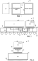
- FIG. 1 is a system 10 with at least two integrated circuits.
- the system 10 includes a first integrated circuit 12 and a second integrated circuit 14, which may complement the functioning of each other.
- the second integrated circuit 14 may be a peripheral integrated circuit supporting the first integrated circuit 12 or vice versa.
- the peripheral integrated circuit describes an integrated circuit that supports the functionality of another integrated circuit.
- the integrated circuits 12 and 14 may be a wide variety of integrated circuits, such as field-programmable gate arrays (FPGA), application-specific integrated circuits (ASIC), system on a chip (SoC), transceivers (e.g., optical module), memory modules and the like.
- FPGA field-programmable gate arrays
- ASIC application-specific integrated circuits
- SoC system on a chip
- transceivers e.g., optical module
- memory modules and the like.
- the second integrated circuit 14 includes programmable logic 16 and a primary circuitry 18.
- the programmable logic 16 may be embedded in the second integrated circuit 14.
- the primary circuitry 18 describes the base functionality of the second integrated circuit 14.
- the primary circuitry 18 may be memory that stores and/or fetches data.
- the programmable logic 16 may be programmed to implement functions such as data/address manipulation, configuration/testing, computation, or any combination thereof.
- the programmable logic 16 may be programmed through various methods. For example, the programmable logic 16 may be programmed via configuration memory.
- the programmable logic 16 is a field programmable gate array (FPGA) fabric.
- the programmable logic 16 may be programmed via metal programmable logic.
- the programmable logic 16 may be HardCopy ASICs.
- the method used to program the programmable logic 16 may enable the programmable logic 16 to be statically or dynamically programmed.
- the programmable logic 16 can be dynamically programmed/reprogrammed during operation.
- the programmable logic may be wholly or partially programmed during operation.
- the programmable logic 16 may also be statically programmed during power up to retain the same programming during operation.
- the first integrated circuit 12 and the second integrated circuit 14 are communicatively coupled.
- the system 10 may utilize a configuration in which the first integrated circuit 12 and the second integrated circuit 14 are both coupled to a printed circuit board (PCB) through a wire bonding process.
- An alternative configuration may communicatively couple the first integrated circuit 12 and the second integrated circuit 14 via an interposer 20 (e.g., in a 2.5D configuration).
- the first integrated circuit 12 and the second integrated circuit 14 may communicate through microbumps 22 joined to the interposer 20.
- the microbumps 22 connect the integrated circuits 12 and 14 to chip-to-chip interconnects 24 within the interposer 20.
- interposer 20 may be an active interposer, which enables the programmable logic 16 to be embedded within the interposer 20. Additionally or alternatively, the interposer 20 may be a passive interposer and the programmable logic 16 may be embedded in the second integrated circuit 14. Furthermore, through-silicon vias (TSVs) 23 may connect certain of the microbumps 22 and/or chip-to-chip interconnects 24 to C4 interconnects 25.
- TSVs through-silicon vias
- FIG. 3 Another alternate configuration of the system 10 is depicted in FIG. 3 .
- the second integrated circuit 14 is stacked on the first integrated circuit 12 (i.e., in a 3D configuration).
- the programmable logic 16 may be located between the first integrated circuit 12 and the second integrated circuit 14 (i.e., embedded between the integrated circuits 12 and 14).
- microbumps 22 may be used to connect the integrated circuits 12 and 14 to the programmable logic 16.
- chip-to-chip interconnects and/or TSVs may run through the programmable logic 16 to provide communication channels between the integrated circuits 12 and 14.
- the programmable logic 16 may be included in the second integrated circuit 14 similar to FIG. 1 , and the integrated circuits 12 and 14 may be directly interconnected via microbumps and/or TSVs.
- the first integrated circuit 12 is communicatively coupled to the second integrated circuit 14, such as a memory module 14A, which is depicted in FIG. 4 .
- the memory module 14A may be a single memory die, memory dies stacked with programmable logic, or a stack of memory with embedded programmable logic.
- the memory 14A for example, may be static random-access memory (SRAM), dynamic random-access memory (DRAM), thyristor random-access memory (T-RAM), or any combination thereof.
- the memory 14A includes the programmable logic 16, a configuration port 26, and the primary circuitry 18.
- the primary circuitry 18 refers to the components of the integrated circuit that facilitate the base functions of the integrated circuits.
- the primary circuitry 18 may perform the reading and writing to the memory 14A.
- the memory module 14A may complement and/or support the functionality of an FPGA, an ASIC, or the like (i.e., a peripheral integrated circuit).
- the first integrated circuit 12 and the memory module are coupled, which may enable the integrated circuits 12 and 14 to communicate address signals, data signals, command signals, control signals, configuration signals, or any combination thereof.
- the address signals may specify an address to read and/or write data, which may be communicated via an address bus 13.
- the data read or to be written may be included in the data signals and communicated via a data bus 15.
- the control signals and command signals may be communicated via a control bus 17 and a command bus 19.
- the first integrated circuit 12 may instruct the memory 14A to perform a specific action, such as reading data at a memory address.
- the configuration signals may be communicated via configuration buses 28.
- the configuration signals may include instructions to configure the integrated circuits 12 and 14.
- the configuration bus 28 is coupled to the first integrated circuit 12, to the memory 14A, and between the two.
- the first integrated circuit 12 may receive configuration signals from another device, such as a supervising controller, which instructs the first integrated circuit 12 to transmit a second configuration signal to the memory 14A.
- the first integrated circuit 12 may determine itself to send configuration signals to the memory 14A.
- the memory 14A may directly receive configuration signals from another device. Accordingly, the configuration signals may be communicated between the integrated circuits 12 and 14 or from a controlling device, such as an operator utilizing a computing device to communicate with the integrate circuits 12 and 14.
- the programmable logic 16 may be programmed to enhance the base functions of the memory 14A.
- the programmable logic 16 may implement data/address manipulation functions, configuration/testing functions, computational functions, or any combination thereof.
- the data/address manipulation functions may include incrementing/decrementing memory addresses, caching data, configuring memory ports, configuring memory modes, controlling the memory, or any combination thereof.
- the computational functions may include matching patterns, determining statistics, or any combination thereof.
- the configuration/testing functions may include built-in self-tests, debugging, performance characterization during wafer sort or final testing, or any combination thereof.
- the programmable logic 16 may be programmed accordingly through configuration signals.
- the memory 14A may receive configuration signals at the configuration port 26, which is communicatively coupled to the configuration busses 28 carrying the configuration signals.
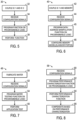
- FIG. 5 illustrates a process 30 for performing functions (e.g., data/address manipulation functions, configuration/testing functions, computational functions) on the second integrated circuit (e.g., memory 14A) 14.
- the process 30 may begin by coupling the first integrated circuit 12 and the second integrated circuit 14 (process block 32).
- the first integrated circuit 12 and the second integrated circuit 14 may be coupled in various manners, such as through to a printed circuit board (PCB) or through an interposer 20.
- the second integrated circuit 14 may receive configuration signals (process block 34).
- the configuration signals may include instructions relating to the function.
- the configuration signals may be transmitted to the second integrated circuit 14 from the first integrated circuit 12 or another device based on the function to be implemented in the integrated circuits 12 and 14.
- the second integrated circuit 14 may program the function on the programmable logic 16 (process block 36).
- the programmable logic 16 may be programmed to increment/decrement memory addresses, cache data, configure memory ports, configure memory modes/technologies, controlling the memory, or any combination thereof.
- block 32 may follow blocks 34 and 36.
- the programmable logic 16 may be programmed before being coupled to the first integrated circuit 12.
- the programmable logic 16 may perform the function (process block 38).
- a process 40 for implementing a data/address function i.e., configuring memory modes and/or memory ports
- the memory modes and/or memory ports may facilitate the functionality of the first integrated circuit 12.
- process 40 may begin by coupling the first integrated circuit and the memory 14A (process block 42).
- the memory 14A may receive configuration signals (process block 44).
- the first integrated circuit 12 e.g., an FPGA or an ASIC
- the first integrated circuit 12 may send configuration signals to the memory 14A, via the configuration bus 28, to instruct the configuration of the memory 14A.
- the programmable logic 16 may be programmed (process block 45) and configure the memory mode(s) and/or memory port(s) accordingly (process block 46).
- the memory 14A may be programmed in different modes to better facilitate the functions of the first integrated circuit 12.
- the programmable logic 16 may implement various memory modes in the entire or part of the memory 14A.
- the programmable logic 16 may configure the entire memory 14A as SRAM, or alternatively, the programmable logic 16 may configure a first portion of the memory 14A to operate as SRAM and a second portion to operate as T-RAM.
- the memory ports may be programmed to alter the read or write bandwidth of the memory 14A based on the functionality of the first integrated circuit 12.
- the programmable logic 16 may configure memory ports as read ports or as write ports. For example, if the memory 14A has four ports, when the first integrated circuit 12 utilizes a larger write bandwidth, the programmable logic 16 may configure three of the memory ports as write ports and one as a read port. Alternatively, if the first integrated circuit 12 utilizes a larger read bandwidth, the programmable logic 16 may configure three of the memory ports as read ports and one as a write port. This configuration may be useful when the first integrated circuit 12 is implementing wireline applications, which utilize a higher read bandwidth than write bandwidth.
- the programmable logic 16 embedded in the second integrated circuit 14 may perform configuration/testing functions.
- the programmable logic 16 may facilitate a wafer testing process 48 during wafer sort testing and/or final testing.
- the process 48 may begin by fabricating the wafer (process block 50). Specifically, this may include fabricating the primary circuitry 18 and embedding the programmable logic 16.
- the second integrated circuit 14 may receive the configuration signals (process block 52).
- the second integrated circuit 14 may receive configuration signals from a central wafer testing device via the configuration bus 28.
- the central wafer testing device may transmit configuration signals to the memory 14A instructing the programmable logic 16 on a wafer testing function.
- the wafer testing functions may include self-tests, debugging, performance characterization, or any combination thereof.
- the wafer testing function may be programmed into the programmable logic (process block 54).
- the programmable logic 16 may perform the wafer testing function (process block 56).
- programmable logic 16 may self test the second integrated circuit 14 to determine if the second integrated circuit 14 is functioning properly. Additionally, the programmable logic 16 may be programmed to debug the second integrated circuit 14 when it is not functioning properly.
- FIG. 6 depicts a process 58 for testing the memory's performance and compensating accordingly.
- the process 58 may begin by receiving configuration signals (process block 60).
- the configuration signals may include instructions for characterizing the performance of the memory 14A and instructions to compensate for the performance.
- the configuration signals may come from the first integrated circuit 12 or another device concerned with the performance of the memory module 14A.
- a testing device may send configuration signals to various memory modules 14A to test performance of each.
- the programmable logic 16 may be programmed to run the performance characterization function (process block 62) and the programmable logic 16 may perform the performance characterization function (process block 64). For example, the programmable logic 16 may test each bit to determine whether the memory 14A is properly storing data. Finally, based on the performance characterization, the programmable logic 16 may compensate accordingly (process block 66). For example, if it is determined that the capacitors in the memory 14A are not storing enough charge, the power supplied to the memory module 14A may be increased.
- a second integrated circuit 14B includes a chip-to-chip interface.
- the second integrated circuit 14B may be an ASIC or a transceiver (e.g., optical module), such as a Thunderbolt module available from Intel Corporation, of Santa Clara, California.
- the second integrated circuit 14B may include a data connection 67 (e.g., an optical connector) to couple with an optical cable.
- the second integrated circuit 14B e.g., optical module
- the second integrated circuit 14B may complement and/or support the functionality of an FPGA, an ASIC, or the like (i.e., a peripheral integrated circuit).
- the system 10 depicted in FIG. 4 includes the data bus 15 to transmit data between the first integrated circuit 12 and the second integrated circuit 14B.
- the system 10 also similarly includes the command bus 19 and the control bus 17 to communicate control signals and command signals between the first integrated circuit 12 and the second integrated circuit 14B.
- the configuration bus 28 is coupled to the first integrated circuit 12, to the second integrated circuit 14B, and between the two to facilitate the transmission of configuration signals.
- the second integrated circuit 14B includes the programmable logic 16 to enhance the functionality of the primary circuit, the configuration port 26 to receive configuration signals from the configuration bus 28, and the primary circuitry 18.
- the second integrated circuit 14B is a transceiver (e.g., optical IO module or electrical IO module)
- the primary circuitry 18 may transmit and receive data from other devices.
- the first integrated circuit 12 includes a first chip-to-chip interface 68, such as a first universal interface block (UIB 1) 68
- the second integrated circuit 14B includes a second chip-to-chip interface 70, such as a second universal interface block (UIB2) 70.
- Different chip-to-chip interfaces e.g., 68 and 70
- FIG. 10 depicts a process 72 to perform computational functions (e.g., interfacing functions) to facilitate interfacing the integrated circuits (i.e., 12 and 14B).
- UIB 1 and UIB2 are merely illustrative and the techniques taught herein may be applied to various chip-to-chip interfaces.
- the process 72 may begin by coupling the first integrated circuit 12 and the second integrated circuit 14B (process block 74).
- the integrated circuits i.e., 12 and 14B
- the second integrated circuit 14B may receive configuration signals (process block 76).
- the configuration signals may include instructions for performing computational functions, such as converting from UIB 1 to UIB2. Accordingly, the configuration signals may be transmitted from the first integrated circuit 12 or another device.
- UIB2 may include a backward compatibility function that instructs older chip-to-chip interfaces (e.g., UIB 1) on how to interface with UIB 2 70 via the configuration signals.
- UIB 1 a backward compatibility function that instructs older chip-to-chip interfaces
- the programmable logic 16 may be programmed with computational functions (process block 78). Similar to processes described above (i.e., 30 and 40), the second integrated circuit 14B may receive the configuration signals and program the programmable logic 16 before being coupled to the first integrated circuit 12.
- the programmable logic 16 may determine operational parameters for both integrated circuits (i.e., 12 and 14B) (process block 80). In other words, the programmable logic 16 determines the operational parameter of the integrated circuits (i.e., 12 and 14B) that may be interfaced. For example, this may include polling the first integrated circuit 12 and the primary circuitry 18 in the second integrated circuit 14A for the chip-to-chip interface used in each. Finally, the programmable logic 16 performs the computational function (e.g., interfacing function) in the second integrated circuit 14B (process block 82). Following the example presented above, the programmable logic 16 can absorb interface protocol mismatches between chip-to-chip interfaces (e.g., UIB1 and UIB2) to enable seamless integration. More specifically, the programmable logic 16 adjusts the second integrated circuit 14B based on the chip-to-chip interface of the first integrated circuit 12.
- the programmable logic 16 can absorb interface protocol mismatches between chip-to-chip interfaces (e.g.,
- computational functions may include synchronizing the integrated circuits, facilitating handshaking between the integrated circuits, interface protocol conversion, throughput matching (i.e., aggregation or fanout), and the like.
- an interface protocol conversion function may convert between an Advanced eXtensible Interface (AXI) interface protocol to an Avalon interface protocol.
- AXI interface protocol is available from ARM Holdings PLC, of Cambridge, England, and the Avalon interface protocol is available from Altera Corporation, of San Jose, California.
- the computational functions may further include encryption/decryption, encoding/decoding, forward error correction, signal conditioning, signal detection, and the like.
- the programmable logic 16 may encrypt data before the primary circuitry 18 sends that data through a data connection 67 (e.g., an optical connector). Conversely, the programmable logic 16 may also decrypt data received from the data connection 67 and pass the decrypted data to the primary circuitry 18. Accordingly, this may enable the second integrated circuit 14B (e.g., transceiver) to communicate with integrated circuits utilizing various encryption/decryption protocols.
- a data connection 67 e.g., an optical connector
- the programmable logic 16 may perform configuration/testing functions in the second integrated circuit 14B.
- the programmable logic 16 may also test and maintain the transceiver (e.g., optical module) including the data connection 67.
- a process 84 for testing the second integrated circuited 14B is depicted in FIG. 11 .
- the process 84 may begin by receiving configuration signals (process block 86).
- the configuration files may be transmitted from the first integrated circuit 12 or from another device.
- the configuration signals may include instructions for testing the transceiver (e.g., optical module).
- the configuration signals may instruct the programmable logic 16 to determine whether the data connection 67 is properly representing data that is transmitted. Additionally, the configuration signals may also instruct the programmable logic 16 to maintain the second integrated circuited 14B (e.g., transceiver) in order to reduce the possibility of future malfunctions.
- the testing functions may be programmed onto the programmable logic 16 (process block 88). And finally, the programmable logic 16 may test the second integrated circuited 14B (e.g., transceiver) (process block 90).
- the programmable logic may instruct the primary circuitry 18 (e.g., base transceiver) to transmit a known signal and test the data connection 67 to determine if that is in fact what is being transmitted.
- the system 10 may include various embodiments of the second integrated circuit 14.
- Another example of the second integrated circuit 14, as depicted in FIG. 12 is a system on a chip (SoC) 14C.
- the system 10 includes the data bus 15 to transmit data between the first integrated circuit 12 and the SoC 14C.
- the system 10 includes the command bus 19 and the control bus 17 to communicate control signals and command signals between the first integrated circuit 12 and the SoC 14C.
- the configuration bus 28 is coupled to the SoC 14C to facilitate the transmission of configuration signals from another device.
- the SoC 14C includes the programmable logic 16 to enhance the functionality of the primary circuitry 18, the configuration port 26 to receive configuration signals from the configuration bus 28, and the primary circuitry 18 (i.e., base functions of SoC).
- the first integrated circuit 12 includes the first chip-to-chip interface 68 (e.g., UIB1), and the SoC 14C includes a second chip-to-chip interface 70 (e.g., UIB2).
- the SoC 14C may integrate various computational functions into a single chip.
- the primary circuitry 18 of the SoC 14C may include random access memory (RAM) 92, flash memory 94, a universal serial bus (USB) 96, and other components 98.
- the memory i.e., RAM 92 and flash memory 94
- the USB 96 may act as an external interface.
- each of these components i.e., 92, 94, 96, and 98
- the SoC bus 100 may utilize an interface protocol, such as AXI or Avalon described above.
- the SoC 14C may interface with peripheral devices (i.e., first integrated circuit 12) via the data bus 15, the command bus 19, the control bus 17, or any combination thereof.
- peripherals may be additional memory or a transceiver (e.g., optical IO module or electrical IO module).
- the programmable logic 16 may enhance the functionality of the SoC 14C by performing computational functions (e.g., interfacing functions).
- computational functions e.g., interfacing functions
- process 72 depicted in FIG. 10
- the SoC 14C and the peripheral device 12 may be coupled (process block 74).
- the SoC 14C may receive configuration signals (process block 76).
- the SoC 14C may receive the configuration signals from another device via the configuration bus 28.
- the configuration signals may instruct the programmable logic to perform a computational function.
- one computational function may be to change the interface protocol used on the SoC bus 100 to match the interface protocol used in the peripheral device (i.e., first integrated circuit 12) to facilitate interfacing.
- the programmable logic 16 may change the interface protocol in the SoC bus 100 to Avalon when the interface protocol used in the peripheral device (i.e., first integrated circuit 12) is Avalon.
- the programmable logic 16 may be programmed to perform the computational function (i.e., interfacing function) (process block 78). Once programmed, the programmable logic 16 may determine operational parameters of the peripheral (i.e., first integrated circuit 12) and the SoC 14C (process block 80).
- the programmable logic 16 may poll for various operational parameters. For example, the programmable logic 16 may poll the interface protocols used in the integrated circuits (i.e., 12 and 14C). Specifically, the programmable logic 16 may poll the primary circuitry 18 in the SoC 14C and the peripheral. Finally, the programmable logic 16 may perform the computational function (process block 82).
- process 72 may be utilized to adjust the memory modes the SoC 14C may interface with.
- the programmable logic 16 may adjust the SoC 14C to working with multiple memory modes (e.g., SRAM, DRAM, or T-RAM) to expand the functionality of the SoC 14C.
- the first integrated circuit 12 may also include programmable logic 16 to implement data/address manipulation functions, configuration/testing functions, computational functions, or any combination thereof.
- the programmable logic 16 may be programmed via configuration memory, which may enable the programmable logic 16 to be adjusted even after it has been fabricated. For example, this may enable a user to dynamically adjust the functions of an integrated circuit (e.g., second integrated circuit 14) to account for specific applications, newer technology, malfunctioning components, or the like. Additionally, this may even minimize system downtime by enabling integrated circuit (e.g., second integrated circuit 14) to be programmed while still coupled to the system 10.
- the programmable logic 16 may be programmed via metal programmable logic, which may enable an integrated circuits manufacturer to adjust the functions of the primary circuitry 18 without redesigning the entire integrated circuit.
Landscapes
- Physics & Mathematics (AREA)
- Mathematical Physics (AREA)
- Engineering & Computer Science (AREA)
- Computer Hardware Design (AREA)
- Computing Systems (AREA)
- General Engineering & Computer Science (AREA)
- Semiconductor Integrated Circuits (AREA)
- Logic Circuits (AREA)
Claims (10)
- System (10), umfassend:eine erste integrierte Schaltung (12); undeine zweite integrierte Schaltung (14), die kommunikativ an die erste integrierte Schaltung (12) gekoppelt ist,wobei die zweite integrierte Schaltung (14) umfasst:eine primäre Schaltung (18), die dafür ausgelegt ist, eine Basisfunktionalität der zweiten integrierten Schaltung (14) bereitzustellen;einen Konfigurationsanschluss (26), der dafür ausgelegt ist, Konfigurationssignale von der ersten integrierten Schaltung (12) oder einer anderen Vorrichtung zu empfangen; undeine eingebettete programmierbare Logik (16), gebildet durch eine FPGA (Field-Programmable Gate Array, feldprogrammierbare Gatteranordnung)-Logik;wobei das System dadurch gekennzeichnet ist, dass die zweite integrierte Schaltung (14) dafür konfiguriert ist, die eingebettete programmierbare Logik (16) unter Verwendung der Konfigurationssignale dafür zu programmieren, eine Schnittstellenprotokollumsetzung für ein Protokoll auf einer Chip-zu-Chip-Schnittstelle zwischen der ersten integrierten Schaltung (12) und der zweiten integrierten Schaltung (14) durchzuführen.
- System (10) nach Anspruch 1, wobei die zweite integrierte Schaltung (14) ein integrierte Speichermodulschaltung (14A) ist und
wobei die zweite integrierte Schaltung (14) dafür konfiguriert ist, die eingebettete programmierbare Logik (16) unter Verwendung der Konfigurationssignale zu programmieren, um:eine Daten- oder Adressfunktion zu implementieren, wobei die Daten- oder Adressfunktion das Inkrementieren einer Speicheradresse, das Dekrementieren einer Speicheradresse, das Konfigurieren eines Speicheranschlusses der integrierten Speichermodulschaltung (14), das Konfigurieren eines Speichermodus der integrierten Speichermodulschaltung (14) oder eine beliebige Kombination davon umfasst; oder eine Konfigurations- oder Testfunktion zu implementieren, wobei die Test- oder Konfigurationsfunktion einen integrierten Selbsttest, ein Debugging, eine Leistungscharakterisierung, das Steuern des Speichers oder eine beliebige Kombination davon umfasst; oderüber einen ersten Abschnitt der integrierten Speichermodulschaltung (14) zu verfügen, der als SRAM betrieben wird, und einen zweiten Abschnitt der integrierten Speichermodulschaltung (14), der als T-RAM betrieben wird; oderdie Lese- oder Schreibbandbreite von Speicheranschlüssen der integrierten Speichermodulschaltung (14) anzupassen. - System (10) nach Anspruch 2, wobei die integrierte Speichermodulschaltung (14) eines oder mehrere von SRAM, DRAM und T-RAM aufweist.
- System (10) nach Anspruch 2, wobei die eingebettete programmierbare Logik (16) dafür konfiguriert ist, die Lese- oder Schreibbandbreite von Speicheranschlüssen der integrierten Speichermodulschaltung (14) anzupassen, indem eine Teilmenge der Speicheranschlüsse als Schreibanschlüsse und andere Speicheranschlüsse als Leseanschlüsse konfiguriert werden.
- System nach Anspruch 2, wobei die integrierte Speichermodulschaltung (14) Kondensatoren zum Speichern von Daten umfasst,
wobei die eingebettete programmierbare Logik (16) dafür konfiguriert ist, basierend auf den Konfigurationssignalen, die Datenspeicherleistung der integrierten Speichermodulschaltung (14) zu testen und die der integrierten Speichermodulschaltung zugeführte Leistung (14) in Reaktion auf die getestete Datenspeicherleistung zu erhöhen. - System nach einem der Ansprüche 1 bis 4, wobei die eingebettete programmierbare Logik (16) dafür programmiert ist, eine Rechenfunktion zu implementieren, wobei die Rechenfunktion einen Musterabgleich, das Bestimmen von Statistiken oder beides umfasst.
- System (10) nach einem der Ansprüche 1 bis 5, wobei die eingebettete programmierbare Logik (16) dafür konfiguriert ist, dynamisch programmiert zu werden.
- System (10) nach einem der Ansprüche 1 bis 7, wobei die zweite integrierte Schaltung (14) ein Ein-Chip-System (System on Chip, SoC) (14C) ist.
- System (10) nach einem der Ansprüche 1 bis 7, wobei die zweite integrierte Schaltung (14) ein Speichermodul (14B) ist.
- Verfahren zum Programmieren einer integrierten Schaltung (14), umfassend die Schritte:Empfangen, unter Verwendung einer eingebetteten programmierbaren Logik (16) in der integrierten Schaltung (14), eines Konfigurationssignals von einem Konfigurationsanschluss (26) der integrierte Schaltung (14) von einer anderen integrierten Schaltung (12) oder einer separate Rechenvorrichtung; undProgrammieren der eingebetteten programmierbaren Logik (16), die durch eine FPGA (Field-Programmable Gate Array, feldprogrammierbare Gatteranordnung)-Logik in der integrierten Schaltung (14) gebildet ist, unter Verwendung des empfangenen Konfigurationssignals, wobei das Verfahren dadurch gekennzeichnet, dass das Konfigurationssignal die eingebettete programmierbare Logik (16) in der integrierten Schaltung (14) dafür programmiert, eine Schnittstellenprotokollumsetzung eines Protokolls auf einer Chip-zu-Chip-Schnittstelle zwischen der integrierten Schaltung (12) und der anderen integrierten Schaltung (14) durchzuführen.
Priority Applications (4)
| Application Number | Priority Date | Filing Date | Title |
|---|---|---|---|
| EP14187541.9A EP3002877B1 (de) | 2014-10-02 | 2014-10-02 | Integrierte Schaltvorrichtung mit eingebetteter programmierbarer Logik |
| EP24164807.0A EP4366171A3 (de) | 2014-10-02 | 2014-10-02 | Integrierte schaltungsanordnung mit eingebetteter programmierbarer logik |
| EP24164462.4A EP4362335A3 (de) | 2014-10-02 | 2014-10-02 | Integrierte schaltungsanordnung mit eingebetteter programmierbarer logik |
| EP21176966.6A EP3910798A1 (de) | 2014-10-02 | 2014-10-02 | Integrierte schaltvorrichtung mit eingebetteter programmierbarer logik |
Applications Claiming Priority (1)
| Application Number | Priority Date | Filing Date | Title |
|---|---|---|---|
| EP14187541.9A EP3002877B1 (de) | 2014-10-02 | 2014-10-02 | Integrierte Schaltvorrichtung mit eingebetteter programmierbarer Logik |
Related Child Applications (6)
| Application Number | Title | Priority Date | Filing Date |
|---|---|---|---|
| EP24164462.4A Division EP4362335A3 (de) | 2014-10-02 | 2014-10-02 | Integrierte schaltungsanordnung mit eingebetteter programmierbarer logik |
| EP24164462.4A Division-Into EP4362335A3 (de) | 2014-10-02 | 2014-10-02 | Integrierte schaltungsanordnung mit eingebetteter programmierbarer logik |
| EP24164807.0A Division EP4366171A3 (de) | 2014-10-02 | 2014-10-02 | Integrierte schaltungsanordnung mit eingebetteter programmierbarer logik |
| EP24164807.0A Division-Into EP4366171A3 (de) | 2014-10-02 | 2014-10-02 | Integrierte schaltungsanordnung mit eingebetteter programmierbarer logik |
| EP21176966.6A Division EP3910798A1 (de) | 2014-10-02 | 2014-10-02 | Integrierte schaltvorrichtung mit eingebetteter programmierbarer logik |
| EP21176966.6A Division-Into EP3910798A1 (de) | 2014-10-02 | 2014-10-02 | Integrierte schaltvorrichtung mit eingebetteter programmierbarer logik |
Publications (2)
| Publication Number | Publication Date |
|---|---|
| EP3002877A1 EP3002877A1 (de) | 2016-04-06 |
| EP3002877B1 true EP3002877B1 (de) | 2024-05-08 |
Family
ID=51687835
Family Applications (4)
| Application Number | Title | Priority Date | Filing Date |
|---|---|---|---|
| EP21176966.6A Pending EP3910798A1 (de) | 2014-10-02 | 2014-10-02 | Integrierte schaltvorrichtung mit eingebetteter programmierbarer logik |
| EP14187541.9A Active EP3002877B1 (de) | 2014-10-02 | 2014-10-02 | Integrierte Schaltvorrichtung mit eingebetteter programmierbarer Logik |
| EP24164807.0A Pending EP4366171A3 (de) | 2014-10-02 | 2014-10-02 | Integrierte schaltungsanordnung mit eingebetteter programmierbarer logik |
| EP24164462.4A Pending EP4362335A3 (de) | 2014-10-02 | 2014-10-02 | Integrierte schaltungsanordnung mit eingebetteter programmierbarer logik |
Family Applications Before (1)
| Application Number | Title | Priority Date | Filing Date |
|---|---|---|---|
| EP21176966.6A Pending EP3910798A1 (de) | 2014-10-02 | 2014-10-02 | Integrierte schaltvorrichtung mit eingebetteter programmierbarer logik |
Family Applications After (2)
| Application Number | Title | Priority Date | Filing Date |
|---|---|---|---|
| EP24164807.0A Pending EP4366171A3 (de) | 2014-10-02 | 2014-10-02 | Integrierte schaltungsanordnung mit eingebetteter programmierbarer logik |
| EP24164462.4A Pending EP4362335A3 (de) | 2014-10-02 | 2014-10-02 | Integrierte schaltungsanordnung mit eingebetteter programmierbarer logik |
Country Status (1)
| Country | Link |
|---|---|
| EP (4) | EP3910798A1 (de) |
Families Citing this family (5)
| Publication number | Priority date | Publication date | Assignee | Title |
|---|---|---|---|---|
| KR102381158B1 (ko) * | 2016-08-15 | 2022-03-30 | 자일링크스 인코포레이티드 | 적층형 실리콘 상호 연결(ssi) 기술 통합을 위한 독립형 인터페이스 |
| US11632112B2 (en) | 2017-12-27 | 2023-04-18 | Intel Corporation | Integrated circuit device with separate die for programmable fabric and programmable fabric support circuitry |
| CN115695574B (zh) * | 2022-11-15 | 2025-05-16 | 浪潮电子信息产业股份有限公司 | 一种Avalon协议转换方法、装置、设备及介质 |
| CN115995456A (zh) * | 2023-02-06 | 2023-04-21 | 深圳市奇普乐芯片技术有限公司 | 半导体电路装置及电子设备 |
| CN117034827B (zh) * | 2023-10-08 | 2023-12-15 | 华中科技大学 | 一种用于eFPGA的多路选择器、互连开关及外围接口电路 |
Citations (3)
| Publication number | Priority date | Publication date | Assignee | Title |
|---|---|---|---|---|
| US20030046492A1 (en) * | 2001-08-28 | 2003-03-06 | International Business Machines Corporation, Armonk, New York | Configurable memory array |
| US20050021874A1 (en) * | 2003-07-25 | 2005-01-27 | Georgiou Christos J. | Single chip protocol converter |
| US7474121B1 (en) * | 1998-04-30 | 2009-01-06 | Altera Corporation | Configurable memory design for masked programmable logic |
Family Cites Families (9)
| Publication number | Priority date | Publication date | Assignee | Title |
|---|---|---|---|---|
| US7518398B1 (en) * | 2007-10-04 | 2009-04-14 | Xilinx, Inc. | Integrated circuit with through-die via interface for die stacking |
| US7973555B1 (en) * | 2008-05-28 | 2011-07-05 | Xilinx, Inc. | Configuration interface to stacked FPGA |
| US7930661B1 (en) * | 2008-08-04 | 2011-04-19 | Xilinx, Inc. | Software model for a hybrid stacked field programmable gate array |
| JP2010193325A (ja) * | 2009-02-20 | 2010-09-02 | Mitsubishi Electric Corp | プロトコル変換装置 |
| US8058897B1 (en) * | 2010-06-28 | 2011-11-15 | Xilinx, Inc. | Configuration of a multi-die integrated circuit |
| CN101997745A (zh) * | 2010-11-23 | 2011-03-30 | 珠海市佳讯实业有限公司 | 基于fpga的e1插时隙及e1_ip数据汇聚混合接入装置及方法 |
| US9164147B2 (en) * | 2011-06-16 | 2015-10-20 | Taiwan Semiconductor Manufacturing Co., Ltd. | Method and apparatus for 3D IC test |
| US9026872B2 (en) * | 2012-08-16 | 2015-05-05 | Xilinx, Inc. | Flexible sized die for use in multi-die integrated circuit |
| CN203084708U (zh) * | 2012-12-05 | 2013-07-24 | 楚丰 | 一种以移动设备为基础的集成电路编程系统 |
-
2014
- 2014-10-02 EP EP21176966.6A patent/EP3910798A1/de active Pending
- 2014-10-02 EP EP14187541.9A patent/EP3002877B1/de active Active
- 2014-10-02 EP EP24164807.0A patent/EP4366171A3/de active Pending
- 2014-10-02 EP EP24164462.4A patent/EP4362335A3/de active Pending
Patent Citations (3)
| Publication number | Priority date | Publication date | Assignee | Title |
|---|---|---|---|---|
| US7474121B1 (en) * | 1998-04-30 | 2009-01-06 | Altera Corporation | Configurable memory design for masked programmable logic |
| US20030046492A1 (en) * | 2001-08-28 | 2003-03-06 | International Business Machines Corporation, Armonk, New York | Configurable memory array |
| US20050021874A1 (en) * | 2003-07-25 | 2005-01-27 | Georgiou Christos J. | Single chip protocol converter |
Also Published As
| Publication number | Publication date |
|---|---|
| EP4362335A3 (de) | 2024-10-23 |
| EP4362335A2 (de) | 2024-05-01 |
| EP3002877A1 (de) | 2016-04-06 |
| EP4366171A3 (de) | 2024-07-31 |
| EP4366171A2 (de) | 2024-05-08 |
| EP3910798A1 (de) | 2021-11-17 |
Similar Documents
| Publication | Publication Date | Title |
|---|---|---|
| US12135660B2 (en) | Integrated circuit device with embedded programmable logic | |
| US20250021506A1 (en) | Interface Bridge Between Integrated Circuit Die | |
| JP7599514B2 (ja) | 集積回路パッケージへのプログラマブルデバイスおよび処理システムの集積 | |
| EP4362335A2 (de) | Integrierte schaltungsanordnung mit eingebetteter programmierbarer logik | |
| US10522203B2 (en) | Semiconductor device and system performing calibration operation | |
| US10693568B2 (en) | Adapting serdes receivers to a UFS receiver protocol | |
| US11489527B2 (en) | Three dimensional programmable logic circuit systems and methods | |
| US9613721B2 (en) | Semiconductor memory capable of performing through-chip via test and system using the same | |
| US12332825B2 (en) | Apparatus and method for configuring a interconnect link between chiplets | |
| US20230324981A1 (en) | Usb-c wireless wide area network dongle | |
| CN121464431A (zh) | 在另选模式下用于主带芯片模块连接件的扩展数据链路宽度 | |
| CN111741601A (zh) | 一种通用的可配置的有源基板电路结构 | |
| US8873267B2 (en) | Semiconductor apparatus | |
| TWI465925B (zh) | 不同規格記憶體插槽之電腦系統 | |
| US20260086147A1 (en) | Chiplet testing with lower speed interface | |
| CN105632567A (zh) | 具有嵌入式可编程逻辑的集成电路器件 | |
| WO2025199374A1 (en) | Memory chiplet architecture | |
| US20220337248A1 (en) | Programmable routing bridge | |
| US9170974B2 (en) | Methods and systems for interconnecting host and expansion devices within system-in-package (SiP) solutions | |
| JP6343945B2 (ja) | プログラム可能な論理回路デバイスを備えた電子装置 | |
| CN111478714A (zh) | 一种电子装置及其信号传输方法 |
Legal Events
| Date | Code | Title | Description |
|---|---|---|---|
| PUAI | Public reference made under article 153(3) epc to a published international application that has entered the european phase |
Free format text: ORIGINAL CODE: 0009012 |
|
| AK | Designated contracting states |
Kind code of ref document: A1 Designated state(s): AL AT BE BG CH CY CZ DE DK EE ES FI FR GB GR HR HU IE IS IT LI LT LU LV MC MK MT NL NO PL PT RO RS SE SI SK SM TR |
|
| AX | Request for extension of the european patent |
Extension state: BA ME |
|
| 17P | Request for examination filed |
Effective date: 20161006 |
|
| RBV | Designated contracting states (corrected) |
Designated state(s): AL AT BE BG CH CY CZ DE DK EE ES FI FR GB GR HR HU IE IS IT LI LT LU LV MC MK MT NL NO PL PT RO RS SE SI SK SM TR |
|
| STAA | Information on the status of an ep patent application or granted ep patent |
Free format text: STATUS: EXAMINATION IS IN PROGRESS |
|
| 17Q | First examination report despatched |
Effective date: 20190619 |
|
| REG | Reference to a national code |
Ref country code: DE Ref legal event code: R079 Free format text: PREVIOUS MAIN CLASS: H03K0019177000 Ipc: H03K0019177960 Ref country code: DE Ref legal event code: R079 Ref document number: 602014090121 Country of ref document: DE Free format text: PREVIOUS MAIN CLASS: H03K0019177000 Ipc: H03K0019177960 |
|
| RIC1 | Information provided on ipc code assigned before grant |
Ipc: H03K 19/17796 20200101AFI20231019BHEP |
|
| GRAP | Despatch of communication of intention to grant a patent |
Free format text: ORIGINAL CODE: EPIDOSNIGR1 |
|
| STAA | Information on the status of an ep patent application or granted ep patent |
Free format text: STATUS: GRANT OF PATENT IS INTENDED |
|
| INTG | Intention to grant announced |
Effective date: 20231206 |
|
| GRAS | Grant fee paid |
Free format text: ORIGINAL CODE: EPIDOSNIGR3 |
|
| GRAA | (expected) grant |
Free format text: ORIGINAL CODE: 0009210 |
|
| STAA | Information on the status of an ep patent application or granted ep patent |
Free format text: STATUS: THE PATENT HAS BEEN GRANTED |
|
| AK | Designated contracting states |
Kind code of ref document: B1 Designated state(s): AL AT BE BG CH CY CZ DE DK EE ES FI FR GB GR HR HU IE IS IT LI LT LU LV MC MK MT NL NO PL PT RO RS SE SI SK SM TR |
|
| REG | Reference to a national code |
Ref country code: GB Ref legal event code: FG4D |
|
| REG | Reference to a national code |
Ref country code: CH Ref legal event code: EP |
|
| REG | Reference to a national code |
Ref country code: DE Ref legal event code: R096 Ref document number: 602014090121 Country of ref document: DE |
|
| REG | Reference to a national code |
Ref country code: IE Ref legal event code: FG4D |
|
| P01 | Opt-out of the competence of the unified patent court (upc) registered |
Effective date: 20240506 |
|
| REG | Reference to a national code |
Ref country code: NL Ref legal event code: FP |
|
| REG | Reference to a national code |
Ref country code: LT Ref legal event code: MG9D |
|
| PG25 | Lapsed in a contracting state [announced via postgrant information from national office to epo] |
Ref country code: IS Free format text: LAPSE BECAUSE OF FAILURE TO SUBMIT A TRANSLATION OF THE DESCRIPTION OR TO PAY THE FEE WITHIN THE PRESCRIBED TIME-LIMIT Effective date: 20240908 |
|
| PG25 | Lapsed in a contracting state [announced via postgrant information from national office to epo] |
Ref country code: BG Free format text: LAPSE BECAUSE OF FAILURE TO SUBMIT A TRANSLATION OF THE DESCRIPTION OR TO PAY THE FEE WITHIN THE PRESCRIBED TIME-LIMIT Effective date: 20240508 |
|
| PG25 | Lapsed in a contracting state [announced via postgrant information from national office to epo] |
Ref country code: FI Free format text: LAPSE BECAUSE OF FAILURE TO SUBMIT A TRANSLATION OF THE DESCRIPTION OR TO PAY THE FEE WITHIN THE PRESCRIBED TIME-LIMIT Effective date: 20240508 Ref country code: HR Free format text: LAPSE BECAUSE OF FAILURE TO SUBMIT A TRANSLATION OF THE DESCRIPTION OR TO PAY THE FEE WITHIN THE PRESCRIBED TIME-LIMIT Effective date: 20240508 |
|
| PG25 | Lapsed in a contracting state [announced via postgrant information from national office to epo] |
Ref country code: GR Free format text: LAPSE BECAUSE OF FAILURE TO SUBMIT A TRANSLATION OF THE DESCRIPTION OR TO PAY THE FEE WITHIN THE PRESCRIBED TIME-LIMIT Effective date: 20240809 |
|
| PG25 | Lapsed in a contracting state [announced via postgrant information from national office to epo] |
Ref country code: PT Free format text: LAPSE BECAUSE OF FAILURE TO SUBMIT A TRANSLATION OF THE DESCRIPTION OR TO PAY THE FEE WITHIN THE PRESCRIBED TIME-LIMIT Effective date: 20240909 |
|
| REG | Reference to a national code |
Ref country code: AT Ref legal event code: MK05 Ref document number: 1685859 Country of ref document: AT Kind code of ref document: T Effective date: 20240508 |
|
| PG25 | Lapsed in a contracting state [announced via postgrant information from national office to epo] |
Ref country code: ES Free format text: LAPSE BECAUSE OF FAILURE TO SUBMIT A TRANSLATION OF THE DESCRIPTION OR TO PAY THE FEE WITHIN THE PRESCRIBED TIME-LIMIT Effective date: 20240508 |
|
| PG25 | Lapsed in a contracting state [announced via postgrant information from national office to epo] |
Ref country code: AT Free format text: LAPSE BECAUSE OF FAILURE TO SUBMIT A TRANSLATION OF THE DESCRIPTION OR TO PAY THE FEE WITHIN THE PRESCRIBED TIME-LIMIT Effective date: 20240508 |
|
| PG25 | Lapsed in a contracting state [announced via postgrant information from national office to epo] |
Ref country code: PL Free format text: LAPSE BECAUSE OF FAILURE TO SUBMIT A TRANSLATION OF THE DESCRIPTION OR TO PAY THE FEE WITHIN THE PRESCRIBED TIME-LIMIT Effective date: 20240508 |
|
| PG25 | Lapsed in a contracting state [announced via postgrant information from national office to epo] |
Ref country code: LV Free format text: LAPSE BECAUSE OF FAILURE TO SUBMIT A TRANSLATION OF THE DESCRIPTION OR TO PAY THE FEE WITHIN THE PRESCRIBED TIME-LIMIT Effective date: 20240508 |
|
| PG25 | Lapsed in a contracting state [announced via postgrant information from national office to epo] |
Ref country code: PT Free format text: LAPSE BECAUSE OF FAILURE TO SUBMIT A TRANSLATION OF THE DESCRIPTION OR TO PAY THE FEE WITHIN THE PRESCRIBED TIME-LIMIT Effective date: 20240909 Ref country code: PL Free format text: LAPSE BECAUSE OF FAILURE TO SUBMIT A TRANSLATION OF THE DESCRIPTION OR TO PAY THE FEE WITHIN THE PRESCRIBED TIME-LIMIT Effective date: 20240508 Ref country code: NO Free format text: LAPSE BECAUSE OF FAILURE TO SUBMIT A TRANSLATION OF THE DESCRIPTION OR TO PAY THE FEE WITHIN THE PRESCRIBED TIME-LIMIT Effective date: 20240808 Ref country code: LV Free format text: LAPSE BECAUSE OF FAILURE TO SUBMIT A TRANSLATION OF THE DESCRIPTION OR TO PAY THE FEE WITHIN THE PRESCRIBED TIME-LIMIT Effective date: 20240508 Ref country code: IS Free format text: LAPSE BECAUSE OF FAILURE TO SUBMIT A TRANSLATION OF THE DESCRIPTION OR TO PAY THE FEE WITHIN THE PRESCRIBED TIME-LIMIT Effective date: 20240908 Ref country code: HR Free format text: LAPSE BECAUSE OF FAILURE TO SUBMIT A TRANSLATION OF THE DESCRIPTION OR TO PAY THE FEE WITHIN THE PRESCRIBED TIME-LIMIT Effective date: 20240508 Ref country code: GR Free format text: LAPSE BECAUSE OF FAILURE TO SUBMIT A TRANSLATION OF THE DESCRIPTION OR TO PAY THE FEE WITHIN THE PRESCRIBED TIME-LIMIT Effective date: 20240809 Ref country code: FI Free format text: LAPSE BECAUSE OF FAILURE TO SUBMIT A TRANSLATION OF THE DESCRIPTION OR TO PAY THE FEE WITHIN THE PRESCRIBED TIME-LIMIT Effective date: 20240508 Ref country code: ES Free format text: LAPSE BECAUSE OF FAILURE TO SUBMIT A TRANSLATION OF THE DESCRIPTION OR TO PAY THE FEE WITHIN THE PRESCRIBED TIME-LIMIT Effective date: 20240508 Ref country code: BG Free format text: LAPSE BECAUSE OF FAILURE TO SUBMIT A TRANSLATION OF THE DESCRIPTION OR TO PAY THE FEE WITHIN THE PRESCRIBED TIME-LIMIT Effective date: 20240508 Ref country code: AT Free format text: LAPSE BECAUSE OF FAILURE TO SUBMIT A TRANSLATION OF THE DESCRIPTION OR TO PAY THE FEE WITHIN THE PRESCRIBED TIME-LIMIT Effective date: 20240508 Ref country code: RS Free format text: LAPSE BECAUSE OF FAILURE TO SUBMIT A TRANSLATION OF THE DESCRIPTION OR TO PAY THE FEE WITHIN THE PRESCRIBED TIME-LIMIT Effective date: 20240808 |
|
| PG25 | Lapsed in a contracting state [announced via postgrant information from national office to epo] |
Ref country code: DK Free format text: LAPSE BECAUSE OF FAILURE TO SUBMIT A TRANSLATION OF THE DESCRIPTION OR TO PAY THE FEE WITHIN THE PRESCRIBED TIME-LIMIT Effective date: 20240508 |
|
| PG25 | Lapsed in a contracting state [announced via postgrant information from national office to epo] |
Ref country code: EE Free format text: LAPSE BECAUSE OF FAILURE TO SUBMIT A TRANSLATION OF THE DESCRIPTION OR TO PAY THE FEE WITHIN THE PRESCRIBED TIME-LIMIT Effective date: 20240508 |
|
| PG25 | Lapsed in a contracting state [announced via postgrant information from national office to epo] |
Ref country code: CZ Free format text: LAPSE BECAUSE OF FAILURE TO SUBMIT A TRANSLATION OF THE DESCRIPTION OR TO PAY THE FEE WITHIN THE PRESCRIBED TIME-LIMIT Effective date: 20240508 |
|
| PG25 | Lapsed in a contracting state [announced via postgrant information from national office to epo] |
Ref country code: SK Free format text: LAPSE BECAUSE OF FAILURE TO SUBMIT A TRANSLATION OF THE DESCRIPTION OR TO PAY THE FEE WITHIN THE PRESCRIBED TIME-LIMIT Effective date: 20240508 Ref country code: RO Free format text: LAPSE BECAUSE OF FAILURE TO SUBMIT A TRANSLATION OF THE DESCRIPTION OR TO PAY THE FEE WITHIN THE PRESCRIBED TIME-LIMIT Effective date: 20240508 |
|
| PG25 | Lapsed in a contracting state [announced via postgrant information from national office to epo] |
Ref country code: SM Free format text: LAPSE BECAUSE OF FAILURE TO SUBMIT A TRANSLATION OF THE DESCRIPTION OR TO PAY THE FEE WITHIN THE PRESCRIBED TIME-LIMIT Effective date: 20240508 |
|
| PG25 | Lapsed in a contracting state [announced via postgrant information from national office to epo] |
Ref country code: SM Free format text: LAPSE BECAUSE OF FAILURE TO SUBMIT A TRANSLATION OF THE DESCRIPTION OR TO PAY THE FEE WITHIN THE PRESCRIBED TIME-LIMIT Effective date: 20240508 Ref country code: SK Free format text: LAPSE BECAUSE OF FAILURE TO SUBMIT A TRANSLATION OF THE DESCRIPTION OR TO PAY THE FEE WITHIN THE PRESCRIBED TIME-LIMIT Effective date: 20240508 Ref country code: RO Free format text: LAPSE BECAUSE OF FAILURE TO SUBMIT A TRANSLATION OF THE DESCRIPTION OR TO PAY THE FEE WITHIN THE PRESCRIBED TIME-LIMIT Effective date: 20240508 Ref country code: EE Free format text: LAPSE BECAUSE OF FAILURE TO SUBMIT A TRANSLATION OF THE DESCRIPTION OR TO PAY THE FEE WITHIN THE PRESCRIBED TIME-LIMIT Effective date: 20240508 Ref country code: DK Free format text: LAPSE BECAUSE OF FAILURE TO SUBMIT A TRANSLATION OF THE DESCRIPTION OR TO PAY THE FEE WITHIN THE PRESCRIBED TIME-LIMIT Effective date: 20240508 Ref country code: CZ Free format text: LAPSE BECAUSE OF FAILURE TO SUBMIT A TRANSLATION OF THE DESCRIPTION OR TO PAY THE FEE WITHIN THE PRESCRIBED TIME-LIMIT Effective date: 20240508 |
|
| PG25 | Lapsed in a contracting state [announced via postgrant information from national office to epo] |
Ref country code: IT Free format text: LAPSE BECAUSE OF FAILURE TO SUBMIT A TRANSLATION OF THE DESCRIPTION OR TO PAY THE FEE WITHIN THE PRESCRIBED TIME-LIMIT Effective date: 20240508 |
|
| REG | Reference to a national code |
Ref country code: DE Ref legal event code: R097 Ref document number: 602014090121 Country of ref document: DE |
|
| PLBE | No opposition filed within time limit |
Free format text: ORIGINAL CODE: 0009261 |
|
| STAA | Information on the status of an ep patent application or granted ep patent |
Free format text: STATUS: NO OPPOSITION FILED WITHIN TIME LIMIT |
|
| 26N | No opposition filed |
Effective date: 20250211 |
|
| PG25 | Lapsed in a contracting state [announced via postgrant information from national office to epo] |
Ref country code: SI Free format text: LAPSE BECAUSE OF FAILURE TO SUBMIT A TRANSLATION OF THE DESCRIPTION OR TO PAY THE FEE WITHIN THE PRESCRIBED TIME-LIMIT Effective date: 20240508 |
|
| REG | Reference to a national code |
Ref country code: CH Ref legal event code: PL |
|
| GBPC | Gb: european patent ceased through non-payment of renewal fee |
Effective date: 20241002 |
|
| PG25 | Lapsed in a contracting state [announced via postgrant information from national office to epo] |
Ref country code: MC Free format text: LAPSE BECAUSE OF FAILURE TO SUBMIT A TRANSLATION OF THE DESCRIPTION OR TO PAY THE FEE WITHIN THE PRESCRIBED TIME-LIMIT Effective date: 20240508 |
|
| PG25 | Lapsed in a contracting state [announced via postgrant information from national office to epo] |
Ref country code: GB Free format text: LAPSE BECAUSE OF NON-PAYMENT OF DUE FEES Effective date: 20241002 |
|
| PG25 | Lapsed in a contracting state [announced via postgrant information from national office to epo] |
Ref country code: BE Free format text: LAPSE BECAUSE OF NON-PAYMENT OF DUE FEES Effective date: 20241031 Ref country code: LU Free format text: LAPSE BECAUSE OF NON-PAYMENT OF DUE FEES Effective date: 20241002 |
|
| PG25 | Lapsed in a contracting state [announced via postgrant information from national office to epo] |
Ref country code: FR Free format text: LAPSE BECAUSE OF NON-PAYMENT OF DUE FEES Effective date: 20241031 |
|
| PG25 | Lapsed in a contracting state [announced via postgrant information from national office to epo] |
Ref country code: CH Free format text: LAPSE BECAUSE OF NON-PAYMENT OF DUE FEES Effective date: 20241031 |
|
| REG | Reference to a national code |
Ref country code: BE Ref legal event code: MM Effective date: 20241031 |
|
| PG25 | Lapsed in a contracting state [announced via postgrant information from national office to epo] |
Ref country code: SE Free format text: LAPSE BECAUSE OF FAILURE TO SUBMIT A TRANSLATION OF THE DESCRIPTION OR TO PAY THE FEE WITHIN THE PRESCRIBED TIME-LIMIT Effective date: 20240508 |
|
| PGFP | Annual fee paid to national office [announced via postgrant information from national office to epo] |
Ref country code: NL Payment date: 20250912 Year of fee payment: 12 |
|
| PG25 | Lapsed in a contracting state [announced via postgrant information from national office to epo] |
Ref country code: IE Free format text: LAPSE BECAUSE OF NON-PAYMENT OF DUE FEES Effective date: 20241002 |
|
| PGFP | Annual fee paid to national office [announced via postgrant information from national office to epo] |
Ref country code: DE Payment date: 20250916 Year of fee payment: 12 |
|
| PG25 | Lapsed in a contracting state [announced via postgrant information from national office to epo] |
Ref country code: CY Free format text: LAPSE BECAUSE OF FAILURE TO SUBMIT A TRANSLATION OF THE DESCRIPTION OR TO PAY THE FEE WITHIN THE PRESCRIBED TIME-LIMIT; INVALID AB INITIO Effective date: 20141002 |
|
| PG25 | Lapsed in a contracting state [announced via postgrant information from national office to epo] |
Ref country code: HU Free format text: LAPSE BECAUSE OF FAILURE TO SUBMIT A TRANSLATION OF THE DESCRIPTION OR TO PAY THE FEE WITHIN THE PRESCRIBED TIME-LIMIT; INVALID AB INITIO Effective date: 20141002 |
|
| PG25 | Lapsed in a contracting state [announced via postgrant information from national office to epo] |
Ref country code: TR Free format text: LAPSE BECAUSE OF FAILURE TO SUBMIT A TRANSLATION OF THE DESCRIPTION OR TO PAY THE FEE WITHIN THE PRESCRIBED TIME-LIMIT Effective date: 20240508 |
|
| PG25 | Lapsed in a contracting state [announced via postgrant information from national office to epo] |
Ref country code: LT Free format text: LAPSE BECAUSE OF FAILURE TO SUBMIT A TRANSLATION OF THE DESCRIPTION OR TO PAY THE FEE WITHIN THE PRESCRIBED TIME-LIMIT Effective date: 20240508 |