EP3001466A1 - Light-emitting module - Google Patents
Light-emitting module Download PDFInfo
- Publication number
- EP3001466A1 EP3001466A1 EP14801082.0A EP14801082A EP3001466A1 EP 3001466 A1 EP3001466 A1 EP 3001466A1 EP 14801082 A EP14801082 A EP 14801082A EP 3001466 A1 EP3001466 A1 EP 3001466A1
- Authority
- EP
- European Patent Office
- Prior art keywords
- light emitting
- disposed
- upper portion
- emitting module
- optical member
- Prior art date
- Legal status (The legal status is an assumption and is not a legal conclusion. Google has not performed a legal analysis and makes no representation as to the accuracy of the status listed.)
- Granted
Links
Images




Classifications
-
- H—ELECTRICITY
- H10—SEMICONDUCTOR DEVICES; ELECTRIC SOLID-STATE DEVICES NOT OTHERWISE PROVIDED FOR
- H10H—INORGANIC LIGHT-EMITTING SEMICONDUCTOR DEVICES HAVING POTENTIAL BARRIERS
- H10H20/00—Individual inorganic light-emitting semiconductor devices having potential barriers, e.g. light-emitting diodes [LED]
- H10H20/80—Constructional details
- H10H20/85—Packages
- H10H20/8506—Containers
-
- H—ELECTRICITY
- H10—SEMICONDUCTOR DEVICES; ELECTRIC SOLID-STATE DEVICES NOT OTHERWISE PROVIDED FOR
- H10H—INORGANIC LIGHT-EMITTING SEMICONDUCTOR DEVICES HAVING POTENTIAL BARRIERS
- H10H20/00—Individual inorganic light-emitting semiconductor devices having potential barriers, e.g. light-emitting diodes [LED]
- H10H20/80—Constructional details
- H10H20/85—Packages
- H10H20/851—Wavelength conversion means
- H10H20/8511—Wavelength conversion means characterised by their material, e.g. binder
- H10H20/8512—Wavelength conversion materials
-
- H—ELECTRICITY
- H10—SEMICONDUCTOR DEVICES; ELECTRIC SOLID-STATE DEVICES NOT OTHERWISE PROVIDED FOR
- H10H—INORGANIC LIGHT-EMITTING SEMICONDUCTOR DEVICES HAVING POTENTIAL BARRIERS
- H10H20/00—Individual inorganic light-emitting semiconductor devices having potential barriers, e.g. light-emitting diodes [LED]
- H10H20/80—Constructional details
- H10H20/85—Packages
- H10H20/855—Optical field-shaping means, e.g. lenses
-
- H—ELECTRICITY
- H10—SEMICONDUCTOR DEVICES; ELECTRIC SOLID-STATE DEVICES NOT OTHERWISE PROVIDED FOR
- H10W—GENERIC PACKAGES, INTERCONNECTIONS, CONNECTORS OR OTHER CONSTRUCTIONAL DETAILS OF DEVICES COVERED BY CLASS H10
- H10W76/00—Containers; Fillings or auxiliary members therefor; Seals
- H10W76/60—Seals
- H10W76/63—Seals characterised by their shape or disposition, e.g. between cap and walls of a container
Definitions
- An embodiment relates to a light emitting module.
- III group nitrides such as gallium nitride (GaN), aluminum nitride (AlN), and indium gallium nitride (InGaN), are chiefly used in a light-emitting diode (LED) because they have excellent thermal stability and a directly shift energy band structure. Specifically, the III group nitrides are chiefly used in a blue LED and an ultraviolet LED (UV LED).
- GaN gallium nitride
- AlN aluminum nitride
- InGaN indium gallium nitride
- UV LED ultraviolet LED
- UV LED which emits UV rays is packed in a specific body (or case), fabricated, and sold.
- the UV rays emitted by the UV LED may discolor or alter other parts including the body of a light emitting module.
- the discoloration or alteration of the body or other parts attributable to UV rays may have a bad effect on reliability or durability of a light emitting module including an UV LED.
- a light emitting module can prevent an adhesive member from being discolored or altered due to heat or UV rays of a light source unit.
- a light emitting module can prevent a phenomenon in which any metal unstable in first and second adhesive members adheres to the light-emitting surface of a light emitting device of a light source unit when a cover and a body are coupled by eutectic bonding.
- a light emitting module includes a light source unit, a body, an optical member, and an adhesive member.
- the upper portion of the body is disposed between the light emitting device of the light source unit and the adhesive member.
- Such a light emitting module can prevent the adhesive member from being discolored or altered due to heat or UV rays of the light source unit.
- a light emitting module includes a light source unit, an optical member, a body, and an adhesive member.
- the body includes a first cavity in which the light source unit is disposed and a second cavity in which the optical member is disposed.
- the body includes a protrusion disposed in the second cavity. The protrusion is disposed between the light emitting device and the adhesive member.
- Such a light emitting module can prevent the adhesive member from being discolored or altered due to heat or UV rays of the light source unit.
- a light emitting module includes a light source unit, a body, an optical member, a cover, and an adhesive member.
- the upper portion of the body is disposed between the light emitting device of the light source unit and the adhesive member.
- Such a light emitting module can prevent the adhesive member from being discolored or altered due to heat or UV rays of the light source unit.
- a light emitting module includes a light source unit, a body, an optical member, a cover, and an adhesive member.
- the protrusion of the cover is disposed between the light emitting device of the light source unit and the adhesive member.
- Such a light emitting module can prevent the adhesive member from being discolored or altered due to heat or UV rays of the light source unit.
- the adhesive member may include a first adhesive member and a second adhesive member.
- the first adhesive member includes any one selected from the group consisting of gold (Au), nickel (Ni), titanium (Ti), copper (Cu), and chrome (Cr).
- the second adhesive member includes any one selected from the group consisting of tin (Sn), germanium (Ge), silicon (Si), and antimony (Sb) and an alloy including gold (Au) or any one selected from the group consisting of lead (Pb) and silver (Ag) and an alloy including tin (Sn)
- a phenomenon in which any metal unstable in the first and second adhesive members adheres to the light-emitting surface of a light emitting device of the light source unit can be prevented when the cover and the body are coupled by eutectic bonding.
- the adhesive member can be prevented from being discolored or altered due to heat or UV rays of the light source unit.
- the light emitting module according to an embodiment there is an advantage in that a phenomenon in which any metal unstable in the first and second adhesive members adheres to the light-emitting surface of a light emitting device of the light source unit can be prevented when the cover and the body are coupled by eutectic bonding.
- each element is described on the basis of the drawings. Furthermore, in the drawings, the thickness or size of each layer has been enlarged, omitted, or schematically shown for convenience and clarity of description. Furthermore, an actual size is not entirely incorporated into the size of each element.
- the term on (over) or below (under) includes that the two elements have a direct come in contact with each other or one or more other elements are disposed between the two elements (indirectly). Furthermore, if "on (over) or below (under)” is expressed, it may include the meaning of an upward direction or a downward direction on the basis of one element.
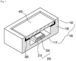
- FIG. 1 is a cross-sectional perspective view of a light emitting module according to a first embodiment
- FIG. 2 is an exploded perspective view of the body and optical member of the light emitting module shown in FIG. 1
- FIG. 3 is a cross-sectional view of the light emitting module shown in FIG. 1 .
- the light emitting module may include a body 100, a light source unit 200, an adhesive member 300, and an optical member 400.
- the light source unit 200, the adhesive member 300, and the optical member 400 are disposed in the body 100. Specifically, the light source unit 200, the adhesive member 300, and the optical member 400 are received in the body 100. In this case, the body 100 is coupled to the optical member 400 through the adhesive member 300.
- the body 100 is described in more detail.
- the body 100 may include a lower portion 110, a wall portion 130, and an upper portion 150.
- the lower portion 110, the wall portion 130, and the upper portion 150 may be made of the same material and integrally formed or may be made of the same or different materials, may be separately fabricated, and may be then coupled together.
- the light source unit 200 and the wall portion 130 may be disposed on the lower portion 110. Specifically, the light source unit 200 and the wall portion 130 may be disposed on the top surface of the lower portion 110. In this case, the light source unit 200 may be disposed in the central part of the top surface of the lower portion 110. The wall portion 130 may be disposed in the outer part of the top surface of the lower portion 110 in such a way as to surround the surroundings of the light source unit 200.
- the lower portion 110 may be a ceramic board of a single layer or a multi-layer.
- the lower portion 110 may be implemented using a high temperature cofired ceramic (HTCC) technology.
- HTCC high temperature cofired ceramic
- ceramic layers may be formed by simultaneous firing at a high temperature of 1200°C or higher.
- the lower portion 110 is the ceramic board of a multi-layer, for example, it may be formed by the HTCC or low temperature cofired ceramics (LTCC). If the lower portion 110 is the ceramic board of a multi-layer, the thickness of the layers may be the same or different, but is not limited thereto. If the lower portion 110 is made of an inorganic ceramic material, although a light source unit emitting deep UV rays or near UV rays having a wavelength of about 200-405 nm is used, reliability can be maintained without a possibility that the lower portion 110 may be discolored or altered due to the UV rays.
- LTCC low temperature cofired ceramics
- the lower portion 110 may be made of an insulating material, such as nitrides or oxides.
- the lower portion 110 may include SiO 2 , Si x O y , Si 3 N y , SiO x N y , Al 2 O 3 , or AlN.
- a material capable of reflecting light is deposited or coated on the top surface of the lower portion 110, in particular, the central part of the top surface in which the light source unit 200 is disposed, thereby being capable of improving light extraction efficiency of the light emitting module according to the first embodiment.
- the wall portion 130 may be disposed on the top surface of the lower portion 110. Specifically, the wall portion 130 may be disposed in the outer part of the top surface of the lower portion 110. The wall portion 130 may be spaced apart from the light source unit 200 at a predetermined interval and may be disposed to surround or beethose the surroundings of the light source unit 200. For example, the wall portion 130 may be disposed in the outer part of the top surface of the lower portion 110 in a shape, such as a circle or a polygon, in such a way as to surround or be protagoniste the surroundings of the light source unit 200, and the shape is not limited thereto.
- the wall portion 130 may include an outer wall exposed to the outside and inner walls surrounding the light source unit 200.
- the inner walls may be vertical to the top surface of the lower portion 110 and may form an obtuse angle or an acute angle with the top surface of the lower portion 110.
- the inner walls may be coated or deposited with a material capable of easily reflecting light emitted by the light source unit 200.
- the wall portion 130 including the inner walls having such a light reflection function may improve light extraction efficiency of the light emitting module according to the first embodiment.
- the wall portion 130 may be a ceramic board including ceramic layers of a single layer or a multi-layer. In this case, if the wall portion 130 is the ceramic board of a multi-layer, the thickness of the layers may be the same or different, but is not limited thereto. If the wall portion 130 is made of an inorganic ceramic material, although a light source unit emitting deep UV rays or near UV rays having a wavelength of about 200-405 nm is used, reliability can be maintained without a possibility that the lower portion 130 may be discolored or altered due to the UV rays.
- the light emitting module according to the first embodiment may include a first cavity 135 by the wall portion 130 and the lower portion 110.
- the first cavity 135 may be a space formed by the inner walls of the wall portion 130 and the top surface of the lower portion 110.
- the light source unit 200 may be disposed in the first cavity 135.
- the cavity 135 may be a vacuum state and may be filled with nitrogen (N2) gas or forming gas.
- the upper portion 150 is disposed on the wall portion 130. Specifically, the upper portion 150 may be disposed on the top surface of the wall portion 130. The upper portion 150 may be disposed on the outer portion of the top surface of the wall portion 130.
- the upper portion 150 guides the optical member 400.
- the upper portion 150 may surround the sides of the optical member 400 and guide the optical member 400.
- the internal surfaces of the upper portion 150 may be spaced apart from the sides of the optical member 400 at a predetermined interval or may come in contact with the sides of the optical member 400.
- the upper portion 150 may have a shape, such as a circle or a polygon, depending on the shape of the wall portion 130, but is not limited thereto.
- the upper portion 150 may be a ceramic board including ceramic layers of a single layer or a multi-layer.
- the wall portion 150 is the ceramic board of a multi-layer, the thickness of the layers may be the same or different, but is not limited thereto.
- the light emitting module according to the first embodiment may include a second cavity 155 by the upper portion 150 and the wall portion 130.
- the second cavity 155 may be a space formed by the internal surfaces of the upper portion 150 and the top surface of the wall portion 130.
- the adhesive member 300 and the optical member 400 may be disposed in the second cavity 155.
- the second cavity 155 may be formed on the first cavity 135.
- the width of the second cavity 155 may be greater than that of the first cavity 135 in order to dispose the optical member 400 on the light source unit 200.
- the depth of the second cavity 155 may be smaller than that of the first cavity 135.
- the light emitting device 250 of the light source unit 200 emits deep UV rays having a wavelength of about 200-405 nm, there is no possibility that the body 100 may be discolored or altered due to the UV rays. Accordingly, the light emitting module according to the first embodiment can secure reliability according to UV rays.
- the light source unit 200 is disposed in the body 100. Specifically, the light source unit 200 may be disposed on the top surface of the lower portion 110 and may be disposed within the first cavity 135.
- the light source unit 200 may include a board 210 and the light emitting device 250.
- the board 210 may be a conductive board or an insulating board, and may include a material in which thermal conductivity and a coefficient of thermal expansion have been incorporated, such as Si, SiC, or AIN.
- the board 210 may have a circuit pattern printed on an insulator, and may include a common printed circuit board (PCB), a metal core PCB, a flexible PCB, or a ceramic PCB, for example.
- PCB printed circuit board
- metal core PCB metal core PCB
- flexible PCB flexible PCB
- ceramic PCB ceramic PCB
- a surface of the board 210 may be made of a material which efficiently reflects light or may be coated with a color by which light is efficiently reflected, for example, white or silver.
- the light emitting device 250 is an element emitting UV rays and may be a deep UV LED or a near UV LED using a semiconductor layer of 3 group-5 group elements, for example. Furthermore, the light emitting device 250 may be an LED emitting one or more of blue, green, red, and white.
- the adhesive member 300 is an adhesive material which is interposed between the optical member 400 and the body 100 and couples the optical member 400 and the body 100.
- the adhesive member 300 is disposed between the body 100 and the optical member 400. Specifically, the adhesive member 300 may be disposed on the top surface of the wall portion 130 and on the internal surfaces of the upper portion 150. When the optical member 400 is received in the second cavity 155 of the body 100, the adhesive member 300 may come in contact with part of the sides and bottom surface of the optical member 400.
- the adhesive member 300 may be an organic material.
- the adhesive member 300 of an organic material may bond the body 100 and the optical member 400 more firmly if the body 100 is a ceramic board.
- the adhesive member 300 of an organic material may be cured through an UV curing process, thereby being capable of tightly fixing the body 100 and the optical member 400.
- the optical member 400 transmits direct or indirect light emitted by the light source unit 200.
- the optical member 400 may simply transmit light from the light source unit 200 and may also diffuse or condense the light.
- the optical member 400 may change the wavelength of light from the light source unit 200.
- the optical member 400 may include a wavelength conversion substance, such as a fluorescent substance.
- the optical member 400 may be a light-transmitting material, for example, glass, polycarbonate (PC), or PMMA in order to transmit light from the light source unit 200.
- a light-transmitting material for example, glass, polycarbonate (PC), or PMMA in order to transmit light from the light source unit 200.
- the optical member 400 is disposed on the light source unit 200 and coupled to the body 100. Specifically, the optical member 400 may be disposed on the second cavity 155 formed on the first cavity 135 of the body 100 in which the light source unit 200 is disposed. Part of the sides and bottom surface of the optical member 400 may be bonded by the adhesive member 300, and thus the optical member 400 may be tightly coupled to the body 100. The sides of the optical member 400 may be surrounded by the upper portion 150 and may have a direct contact with the internal surfaces of the upper portion 150.
- the adhesive member 300 may be discolored or altered by heat emitted from the light emitting device 250 of the light source unit 200, or the adhesive member 300 of an organic material may be discolored or altered by deep UV rays emitted by the light emitting device 250 when the light emitting device 250 of the light source unit 200 emits UV rays, in particular, the deep UV rays.
- the discoloration or alteration of the adhesive member 300 may reduce coherence between the body 100 and the optical member 400. This may cause a severe problem which deteriorates durability and reliability of the light emitting module according to the first embodiment.
- a light emitting module capable of solving such a problem is described below with reference to FIGS. 4 to 6 .
- FIG. 4 is a cross-sectional perspective view of a light emitting module according to a second embodiment
- FIG. 5 is an exploded perspective view of the body and optical member of the light emitting module shown in FIG. 4
- FIG. 6 is a cross-sectional view of the light emitting module shown in FIG. 4 .
- the light emitting module according to the second embodiment can prevent the discoloration or alteration of an adhesive member 300' attributable to heat or UV rays emitted by the light emitting device 250.
- the light emitting module according to the second embodiment includes a body 100', a light source unit 200, the adhesive member 300', and an optical member 400.
- the body 100' of the light emitting module according to the second embodiment includes a lower portion 110, a wall portion 130, and two or more upper portions 160 and 170.
- reference numeral 160 is denoted as a first upper portion
- reference numeral 170 is denoted as a second upper portion.
- the top surface of the wall portion 130 Prior to a description of the first upper portion 160 and the second upper portion 170, the top surface of the wall portion 130 is defined below.
- the top surface of the wall portion 130 may include an outer portion in which the first upper portion 160 is disposed, an inner portion in which the second upper portion 170 is disposed, and a middle portion in which the adhesive member 300' is disposed. In this case, the middle portion means a portion disposed between the outer portion and the inner portion.
- the first upper portion 160 is disposed on the wall portion 130. Specifically, the first upper portion 160 may be disposed on the outer portion of the top surface of the wall portion 130
- the first upper portion 160 may guide the optical member 400. Specifically, the first upper portion 160 may surround the sides of the optical member 400 and guide the optical member 160.
- the first upper portion 160 may include external surfaces and internal surfaces.
- the internal surfaces may form a second cavity 155' along with the middle portion of the wall portion 130 and the external surfaces of the second upper portion 170.
- the first upper portion 160 may come in contact with the optical member 400. Specifically, the sides of the optical member 400 may come in contact with the internal surfaces of the first upper portion 160. If the optical member 400 comes in contact with the first upper portion 160, the first upper portion 160 can guide the optical member 400 more tightly. Accordingly, since a specific gap is not formed between the optical member 400 and the first upper portion 160, a foreign substance or water can be prevented from entering the adhesive member 300'.
- the second upper portion 170 is disposed on the wall portion 130. Specifically, the second upper portion 170 is disposed on the inner portion of the top surface of the wall portion 130. Furthermore, the second upper portion 170 is disposed between the light source unit 200 and the adhesive member 300'.
- the second upper portion 170 may come in contact with the optical member 400. More specifically, the top surface of the second upper portion 170 may come in contact with the bottom surface of the optical member 400. When the second upper portion 170 comes in contact with the optical member 400, the second upper portion 170 can stably support the optical member 400.
- the optical member 400 can be stably fixed to and installed in the body, and a reduction in the function of the adhesive member attributable to a foreign substance or water can be prevented.
- the second upper portion 170 may include external surfaces and internal surfaces.
- the internal surfaces may form a first cavity 135' along with the top surface of the lower portion 110 and the inner walls of the wall portion 130.
- the external surfaces may form the second cavity 155' along with the middle portion of the wall portion 130 and the internal surfaces of the first upper portion 160.
- the first cavity 135' is different from the first cavity 135 of the light emitting module according to the first embodiment. Specifically, the first cavity 135' is formed by the top surface of the lower portion 110, the inner walls of the wall portion 130, and the internal surfaces of the second upper portion 170.
- the light source unit 200 is disposed in the first cavity 135'.
- the internal surfaces of the second upper portion 170 may prevent heat and UV rays which are emitted by the light source unit 200 and directed toward the adhesive member 300'. Accordingly, the discoloration or alteration of the adhesive member 300' attributable to heat and UV rays can be blocked.
- the internal surfaces of the second upper portion 170 may be coated or deposited with a material capable of easily reflecting light from the light source unit 200.
- the second upper portion 170 may be a ceramic board including ceramic layers of a single layer or a multi-layer. Furthermore, the second upper portion 170 may have been integrated and formed with the lower portion 110, the wall portion 130, and the first upper portion 160.
- the height of the second upper portion 170 may be smaller than that of the first upper portion 160.
- the height of the first upper portion 160 and the second upper portion 170 means a length from the top surface of the wall portion 130 to the top surface of each of the upper portions 160 and 170.
- the first upper portion 160 and the second upper portion 170 may not come in contact with the optical member 400. This is described with reference to FIG. 7 .
- FIG. 7 is a light emitting module according to a third embodiment and shows a modified example of the light emitting module according to the second embodiment shown in FIG. 6 .
- the light emitting module according to the third embodiment shown in FIG. 7 is different from the light emitting module according to the second embodiment shown in FIG. 6 in a first upper portion 160' and a second upper portion 170'.
- the first upper portion 160' may be spaced apart from an optical member 400 at a predetermined interval.
- the internal surfaces of the first upper portion 160' may be spaced apart from the sides of the optical member 400 at a predetermined interval.
- the second upper portion 170' may be spaced apart from the optical member 400 at a predetermined interval. Specifically, the top surface of the second upper portion 170' may be spaced apart from the bottom surface of the optical member 400 at a predetermined interval.
- the predetermined intervals may be narrow spaces which may be generated when the optical member 400 is installed a body 100'.
- the predetermined intervals are not essentially formed, and the predetermined intervals may not be formed if the optical member 400 is accurately fit into the body 100'.
- both the first upper portion 160' and the second upper portion 170' have been illustrated as being spaced apart from the optical member 400 at a predetermined interval, but this is only an example. Any one of the first upper portion 160' and the second upper portion 170' may be spaced apart from the optical member 400 at a predetermined interval.
- the height of the second upper portion 170 or 170' may be at least 50 ⁇ m or more. If the height of the second upper portion 170 or 170' is 50 ⁇ m or more and the second upper portion 170 or 170' is a ceramic board, there are advantageous effects in the manufacture process of the second upper portion 170 or 170'. Specifically, if the wall portion 130 is a ceramic board made of the same material as the second upper portion 170 or 170', a single ceramic layer for fabricating the second upper portion 170 or 170' can be additionally formed in a process of forming the ceramic wall portion 130 of a multi-layer structure without using a separate process for fabricating the second upper portion 170 or 170'.
- the second upper portion 170 or 170' can be fabricated along with the wall portion 130.
- the height of 50 ⁇ m is a minimum thickness of a single ceramic layer which may be fabricated by a current process when a ceramic board of a multi-layer structure is formed. Accordingly, it is to be noted that the height may be further reduced with the development of the process of forming the ceramic layer.
- the second upper portion 170 or 170' may be called a protrusion extended into the second cavity 155'. Accordingly, compared to the second cavity 155 of the light emitting module according to the first embodiment, the second cavity 155' may have a shape part of which has been removed by the protrusion 170.
- the light emitting modules according to the second to third embodiments can further improve durability and reliability according to heat and UV rays because they can prevent the discoloration or/and alteration of the adhesive member 300' attributable to heat and UV rays.
- FIG. 8 is a light emitting module according to a fourth embodiment and shows a modified example of the light emitting module according to the second embodiment shown in FIG. 6 .
- the light emitting module according to the fourth embodiment shown in FIG. 8 includes 1) a body 100" not having the first upper portion 160 and 2) an optical member 400' having a greater size than the optical member 400, compared to the light emitting module according to the second embodiment shown in FIG. 6 .
- the light emitting module according to the fourth embodiment shown in FIG. 8 is advantageous in that a light extraction area is further increased compared to the light emitting module according to the second embodiment shown in FIG. 6 because the sides of the optical member 400' are extended up to the outer wall of the wall portion 130 and is advantageous in that an additional process is not required because the first upper portion 160 shown in FIG. 6 does not need to be fabricated. Furthermore, since the first upper portion 160 is not present, the optical member 400' and the body 100" can be fixed more tightly because an adhesive member 300" can be used much more.
- the upper portion 170' may be the same as the second upper portion 170' shown in FIG. 7 . However, this is only an example, and the upper portion 170' may support the optical member 400' like the second upper portion 170 shown in FIG. 6 . Specifically, the top surface of the upper portion 170' shown in FIG. 8 may come in contact with the bottom surface of the optical member 400'.
- the light emitting module according to the fourth embodiment shown in FIG. 8 can further improve durability according to heat and UV rays because the discoloration or/and alteration of the adhesive member 300" attributable to heat and UV rays can be prevented.
- FIG. 9 is a cross-sectional perspective view of a light emitting module according to a fifth embodiment
- FIG. 10 is a perspective view showing that the body and cover of the light emitting module shown in FIG. 9 have been separated
- FIG. 11 is a cross-sectional view of the light emitting module shown in FIG. 9 .
- the light emitting module may include a body 100"', a light source unit 200, a first adhesive member 300a, a second adhesive member 300b, a cover 500, and an optical member 600.
- the light source unit 200, the first adhesive member 300a, the second adhesive member 300b, the cover 500, and the optical member 400 are disposed in the body 100"'. Specifically, the light source unit 200 is received in the body 100"', the body 100'" and the cover 500 are coupled through the first adhesive member 300a and the second adhesive member 300b, and the optical member 600 is coupled to the cover 500.
- the structure of the body 100'" is described in more detail.
- the body 100'" may include a lower portion 110 and a wall portion 130.
- the lower portion 110 and the wall portion 130 are the same as the lower portion 110 and the wall portion 130 shown in FIGS. 1 to 8 , and thus a description thereof is omitted.
- the first adhesive member 300a and the second adhesive member 300b are adhesive materials which are disposed between the body 100 and the cover 500 and which couple the body 100 and the cover 500. More specifically, the first and the second adhesive members 300a and 300b may be substances for sealing the body 100 and the cover 500 by eutectic bonding.
- the first adhesive member 300a is disposed in the top surface of the wall portion 130.
- the first adhesive member 300a may be disposed in the entire top surface of the wall portion 130 or may be disposed in part of the top surface of the wall portion 130.
- the first adhesive member 300a may be metal or a substance including metal.
- the first adhesive member 300a may include any one selected from the group consisting of gold (Au), nickel (Ni), titanium (Ti), copper (Cu), and chrome (Cr).
- the second adhesive member 300b is disposed in the bottom surface of the cover 500 and disposed on the first adhesive member 300a.
- the second adhesive member 300b may be disposed in the entire bottom surface of the cover 500 or may be disposed in part of the bottom surface of the cover 500.
- the second adhesive member 300b may be metal or an alloy having a melting point of 260 °C or more. Specifically, the second adhesive member 300b may be a single piece of metal including gold (Au). Furthermore, the second adhesive member 300b may be an alloy, including any one selected from the group consisting of tin (Sn), germanium (Ge), silicon (Si), and antimony (Sb) and gold (Au). Furthermore, the second adhesive member 300b may be an alloy, including any one selected from the group consisting of lead (Pb) and silver (Ag) and tin (Sn). The characteristics of the aforementioned metal or alloy which may be used as the second adhesive member 300b are described in detail as in ⁇ Table 1 >.
- first adhesive member 300a and the second adhesive member 300b may be reversed. That is, the first adhesive member 300a may be disposed on the second adhesive member 300b.
- the body 100 and the cover 500 may be coupled by eutectic bonding.
- eutectic bonding there is an advantage in that the body 100 and the cover 500 can be tightly coupled.
- the cover 500 is disposed on the body 100'" and is coupled to the body 100"' through the first and the second adhesive members 300a and 300b.
- the cover 500 does not transmit light emitted by the light source unit 200 and may include a separate opening which transmits the light.
- the opening may be formed in the central part of the cover 500, and the optical member 600 may be disposed in the opening.
- the cover 500 is a metallic substance and may be a substance that is difficult to be discolored or altered by UV rays.
- the cover 500 may be a single piece of metal including a metallic substance, such as iron (Fe) or nickel (Ni), or an alloy, including a metallic substance, such as iron (Fe) and nickel (Ni).
- the cover 500 may be Kovar.
- a substance capable of easily reflecting light emitted by the light emitting device 250 of the light source unit 200 may be deposited or coated on the cover 500.
- a substance capable of easily reflecting light may be deposited or coated on the bottom surface of the cover 500 and an inner surface defining the opening.
- the optical member 600 is disposed on the light source unit 200 and coupled to the cover 500. Specifically, the optical member 600 may be disposed on the light emitting device 250 and may be disposed in the opening of the cover 500.
- the optical member 600 transmits direct or indirect light emitted by the light source unit 200.
- the optical member 600 may simply transmit light from the light source unit 200 and may also diffuse or condense the light.
- the optical member 600 may be formed of a transparent material and a non-reflecting coating film so that it externally transmits light generated by the light source unit 200 without absorbing the light.
- the optical member 600 may be made of any one of a glass material, including SiO 2 (quartz, UV fused silica), Al 2 O 3 (sapphire), LiF, MgF 2 , CaF 2 , low iron transparent glass, and B2O3, polycarbonate (PC), and PMMA.
- the optical member 600 may change the wavelength of light from the light source unit 200.
- the optical member 600 may include a wavelength conversion substance, such as a fluorescent substance.
- the second adhesive member 300b is an alloy including two pieces of metal
- a phenomenon in which one piece of metal that belongs to the two pieces of metal and that is more unstable adheres to the light-emitting surface of the light emitting device 250 of the light source unit 200 (or a splattering phenomenon) may be generated.
- Such a phenomenon may deteriorate light extraction efficiency of the light emitting module because it reduces the light-emitting area of the light-emitting surface of the light emitting device 250. Accordingly, a light emitting module capable of solving such a problem is described below with reference to FIGS. 12 to 14 .
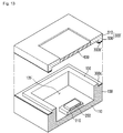
- FIG. 12 is a cross-sectional perspective view of a light emitting module according to a sixth embodiment
- FIG. 13 is a perspective view showing that the body and cover of the light emitting module shown in FIG. 12 have been separated
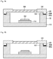
- FIG. 14 is a cross-sectional view of the light emitting module shown in FIG. 12 .
- the light emitting module according to the sixth embodiment can prevent a phenomenon in which one or more of pieces of metal forming a second adhesive member 300b adhere to the light emitting device 250.
- the light emitting module according to the sixth embodiment includes a body 100"", a light source unit 200, first and second adhesive members 300a and 300b, a cover 500', and an optical member 600.
- the body 100"" of the light emitting module according to the sixth embodiment includes a lower portion 110, a wall portion 130, and an upper portion 150.
- the upper portion 150 is disposed on the wall portion 130. Specifically, the upper portion 150 may be disposed in part of the top surface of the wall portion 130. The upper portion 150 may be disposed on the inner portion of the top surface of the wall portion 130. In this case, the top surface of the wall portion 130 may include the inner portion and the outer portion.
- the upper portion 150 may have been upward protruded from the wall portion 130.
- the upper portion 150 may be protruded from the wall portion 130 to the direction of the cover 500.
- the shape of the upper portion 150 may be a shape, such as a circle or a polygon, depending on the shape of the wall portion 130, but is not limited thereto.
- the upper portion 150 may be a ceramic board including ceramic layers of a single layer or a multi-layer.
- the wall portion 150 is the ceramic board of a multi-layer, the thickness of the layers may be the same or different, but is not limited thereto.
- the body 100"" may include a cavity 135'.
- the cavity 135' may be an empty space formed by the internal surfaces of the upper portion 150, the inner walls of the wall portion 130, and the top surface of the lower portion 110.
- the light source unit 200 may be disposed within the cavity 135'.
- the cover 500' may include a cover portion 510 and a protrusion 530.
- the cover portion 510 may have the same shape as the cover 500 shown in FIGS. 9 to 12 .
- the protrusion 530 may have been downward protruded or extended from the bottom surface of the cover portion 510. Specifically, the protrusion 530 may have been protruded or extended from the outer portion of the bottom surface of the cover portion 510 to the outer portion of the top surface of the wall portion 130.
- the protrusion 530 of the cover 500' is disposed on the wall portion 130 of the body 100"" and disposed on the side of the upper portion 150 of the body 100"". Furthermore, the first and the second adhesive members 300a and 300b are disposed between the protrusion 530 of the cover 500' and the wall portion 130 of the body 100"".
- the light emitting module according to the sixth embodiment can prevent one or more of pieces of metal, forming the second adhesive member 300b, from moving to the light emitting device 250 in advance when the body 100"" and the cover 500' are subject to eutectic bonding because the upper portion 150 of the body 100"" is disposed between the second adhesive member 300b and the light emitting device 250. Accordingly, the light emitting module according to the sixth embodiment has an advantage in that light extraction efficiency is not reduced by the second adhesive member 300b upon eutectic bonding. Furthermore, the light emitting module according to the sixth embodiment can prevent the discoloration or alteration of the first and the second adhesive members 300a and 300b because it can block heat and UV rays emitted by the light source unit 200.
- the upper portion 150 may support the cover 500'. This is described with reference to FIG. 15 .
- FIG. 15 is a light emitting module according to a seventh embodiment and shows a modified example of the upper portion 150 shown in FIG. 14 .
- the upper portion 150' shown in FIG. 15 may support the cover 500'. Specifically, the top surface of the upper portion 150' may come in contact with the bottom surface of the cover portion 510 of the cover 500'. If the upper portion 150' supports the cover 500' as described above, the first and the second adhesive members 300a and 300b may have a previously designed height (thickness). This may be useful in cases, such as the following examples. For example, as shown in FIG. 14 , if the upper portion 150 does not support the cover 500', when the cover 500' and the body 100"" are coupled, the protrusion 530 of the cover 500' may become very close to the wall portion 130 of the body 100"" by specific pressure applied to the cover 500'.
- part of the first and the second adhesive members 300a and 300b may overflow between the outer wall of the wall portion 130 and the outer wall of the protrusion 530 or the upper portion 150 and the cover portion 510 by the pressure.
- This may be the unnecessary waste of the first and the second adhesive members 300a and 300b, and the aforementioned problem may occur if part of the first and the second adhesive members 300a and 300b overflows between the upper portion 150 and the cover portion 510. Accordingly, if the upper portion 150' supports the cover 500' as shown in FIG. 15 , the unnecessary waste of the first and the second adhesive members 300a and 300b can be eliminated, and the aforementioned problem can be prevented.
- the light emitting module according to the seventh embodiment can prevent the discoloration or alteration of the first and the second adhesive members 300a and 300b because it can block heat and UV rays emitted by the light source unit 200.
- the height of the upper portion 150' is greater than the height of the protrusion 530. More specifically, the height of the upper portion 150' may be the same as the sum of the height of the protrusion 530 and the height of the first and the second adhesive members 300a and 300b.
- FIG. 16 is a light emitting module according to an eighth embodiment and shows a modified example of the light emitting module according to the sixth embodiment shown in FIG. 14 .
- the light emitting module according to the eighth embodiment shown in FIG. 16 is different from the light emitting module according to the sixth embodiment shown in FIG. 14 in the location of the upper portion 150" of a body 100'"' and the location of the protrusion 530' of a cover 500".
- the upper portion 150" of the body 100'"' of the light emitting module according to the eighth embodiment shown in FIG. 16 is disposed on the outer portion of the top surface of a wall portion 130, and the protrusion 530' of the cover 500" is disposed on the inner portion of the bottom surface of a cover portion 510.
- the protrusion 530' of the cover 500" is disposed on the wall portion 130 of the body 100'"' and disposed on the side of the upper portion 150" of the body 100""'. Furthermore, first and second adhesive members 300a and 300b are disposed between the upper portion 150" of the body 100'"' and the cover portion 510 of the cover 500".
- the light emitting module according to the eighth embodiment can prevent one or more of pieces of metal, forming the second adhesive member 300b, from moving to a light emitting device 250 in advance when the body 100""' and the cover 500" are subject to eutectic bonding because the protrusion 530' of the cover 500" are disposed between the first and the second adhesive members 300a and 300b and the light emitting device 250. Accordingly, like the light emitting module according to the sixth embodiment, the light emitting module according to the eighth embodiment has an advantage in that light extraction efficiency is not reduced by the second adhesive member 300b upon eutectic bonding.
- the light emitting module according to the eighth embodiment may prevent the discoloration or alteration of the first and the second adhesive members 300a and 300b because it can block heat and UV rays emitted by the light source unit 200.
- the height of the protrusion 530' shown in FIG. 16 may be greater than that of the upper portion 150" in order to prevent the unnecessary waste of the first and the second adhesive members 300a and 300b. More specifically, the height of the protrusion 530' may be the same as the sum of the height of the upper portion 150" and the height of the first and the second adhesive members 300a and 300b.
- FIG. 17 is a light emitting module according to a ninth embodiment and shows a modified example of the light emitting module according to the sixth embodiment shown in FIG. 14 .
- the light emitting module according to the ninth embodiment shown in FIG. 17 is different from the light emitting module according to the sixth embodiment shown in FIG. 14 in the upper portions 151 and 153 of a body 100""" and the protrusion 530" of a cover 500"'.
- the upper portions 151 and 153 of the body 100""" of the light emitting module according to the ninth embodiment shown in FIG. 17 includes a first upper portion 151 and a second upper portion 153.
- the first and the second upper portions 151 and 153 are disposed in the top surface of the wall portion 130.
- the first upper portion 151 and the second upper portion 153 are spaced apart from each other.
- the body 100""" may include a groove 155 because the first upper portion 151 and the second upper portion 153 are spaced apart from each other.
- the first and the second upper portions 151 and 153 may have been upward protruded from the top surface of the wall portion 130.
- the first upper portion 151 is disposed on the outer portion of the top surface of the wall portion 130, and the second upper portion 153 is disposed on the inner portion of the top surface of the wall portion 130.
- the cover 500'" includes a cover portion 510 and the protrusion 530".
- the protrusion 530" may have been downward protruded from the middle portion of the bottom surface of the cover portion 510.
- the middle portion of the bottom surface of the cover portion 510 refers to a portion between the inner portion and outer portion of the bottom surface of the cover portion 510.
- the protrusion 530" is disposed between the first upper portion 151 of the body 100""" and the second upper portion 153 of the body 100""". Furthermore, the protrusion 530" may be disposed in the middle portion of the top surface of the wall portion 130 of the body 100""". In this case, the middle portion of the top surface of the wall portion 130 refers to a portion between the inner portion and outer portion of the top surface of the wall portion 130.
- the first and the second adhesive members 300a and 300b are disposed between the protrusion 530" of the cover 500'" and the first upper portion 151 and second upper portion 153 (or the groove 155) of the body 100""".
- the light emitting module according to the ninth embodiment can prevent one or more of pieces of metal, forming the second adhesive member 300b, from moving to the light emitting device 250 in advance when the body 100""" and the cover 500'" are subject to eutectic bonding because the second upper portion 153 of the body 100""" is interposed between the first and the second adhesive members 300a and 300b and the light emitting device 250. Accordingly, like the light emitting module according to the sixth embodiment, the light emitting module according to the ninth embodiment has an advantage in that light extraction efficiency is not reduced by the second adhesive member 300b upon eutectic bonding.
- the light emitting module according to the ninth embodiment may prevent the discoloration or alteration of the first and the second adhesive members 300a and 300b because it can block heat and UV rays emitted by the light source unit 200. Furthermore, the light emitting module according to the ninth embodiment can prevent the alteration of the first and the second adhesive members 300a and 300b attributable to external dust or moisture because the first and the second adhesive members 300a and 300b are not exposed to the outside, unlike the light emitting modules according to the seventh and the eighth embodiments.
- the height of the first and the second upper portions 151 and 153 shown in FIG. 17 may be greater than that of the protrusion 530" in order to prevent the unnecessary waste of the first and the second adhesive members 300 and 400 and to support the cover 500"'. More specifically, the height of the first and the second upper portions 151 and 153 may be the sum of the height of the protrusion 530" and the height of the first and the second adhesive members 300a and 300b.
- each of the height of the upper portion 150, 150', or 150" of the light emitting modules according to the sixth to eighth embodiments and the height of the upper portions 151 and 153 of the light emitting module according to the ninth embodiment may be at least 50 ⁇ m or more. If the height of the upper portion 150, 150', 150", 151, or 153 is 50 ⁇ m or more and the upper portion 150, 150', 150", 151, or 153 is a ceramic board, there are advantageous effects in a process of fabricating the upper portion 150, 150', 150", 151, or 153.
- the wall portion 130 is a ceramic board that is the same material as the upper portion 150, 150', 150", 151, or 153
- a single ceramic layer for fabricating the upper portion 150, 150', 150", 151, or 153 can be additionally formed in a process of forming the ceramic wall portion 130 of a multi-layer structure without using a separate process for fabricating the upper portion 150, 150', 150", 151, or 153. That is, the upper portion 150, 150', 150", 151, or 153 can be formed simultaneously with the wall portion 130 through a single process.
- the height of 50 ⁇ m is a minimum thickness of a single ceramic layer which may be fabricated by a current process when a ceramic board of a multi-layer structure is formed. Accordingly, it is to be noted that the height may be further reduced with the development of the process of forming the ceramic layer.
Landscapes
- Led Device Packages (AREA)
Abstract
Description
- An embodiment relates to a light emitting module.
- III group nitrides, such as gallium nitride (GaN), aluminum nitride (AlN), and indium gallium nitride (InGaN), are chiefly used in a light-emitting diode (LED) because they have excellent thermal stability and a directly shift energy band structure. Specifically, the III group nitrides are chiefly used in a blue LED and an ultraviolet LED (UV LED).
- An UV LED which emits UV rays is packed in a specific body (or case), fabricated, and sold. In this case, the UV rays emitted by the UV LED may discolor or alter other parts including the body of a light emitting module. The discoloration or alteration of the body or other parts attributable to UV rays may have a bad effect on reliability or durability of a light emitting module including an UV LED.
- A light emitting module according to an embodiment can prevent an adhesive member from being discolored or altered due to heat or UV rays of a light source unit.
- A light emitting module according to an embodiment can prevent a phenomenon in which any metal unstable in first and second adhesive members adheres to the light-emitting surface of a light emitting device of a light source unit when a cover and a body are coupled by eutectic bonding.
- A light emitting module according to an embodiment includes a light source unit, a body, an optical member, and an adhesive member. The upper portion of the body is disposed between the light emitting device of the light source unit and the adhesive member. Such a light emitting module can prevent the adhesive member from being discolored or altered due to heat or UV rays of the light source unit.
- A light emitting module according to an embodiment includes a light source unit, an optical member, a body, and an adhesive member. The body includes a first cavity in which the light source unit is disposed and a second cavity in which the optical member is disposed. The body includes a protrusion disposed in the second cavity. The protrusion is disposed between the light emitting device and the adhesive member. Such a light emitting module can prevent the adhesive member from being discolored or altered due to heat or UV rays of the light source unit.
- A light emitting module according to an embodiment includes a light source unit, a body, an optical member, a cover, and an adhesive member. The upper portion of the body is disposed between the light emitting device of the light source unit and the adhesive member. Such a light emitting module can prevent the adhesive member from being discolored or altered due to heat or UV rays of the light source unit.
- A light emitting module according to an embodiment includes a light source unit, a body, an optical member, a cover, and an adhesive member. The protrusion of the cover is disposed between the light emitting device of the light source unit and the adhesive member. Such a light emitting module can prevent the adhesive member from being discolored or altered due to heat or UV rays of the light source unit.
- In the embodiments, the adhesive member may include a first adhesive member and a second adhesive member. The first adhesive member includes any one selected from the group consisting of gold (Au), nickel (Ni), titanium (Ti), copper (Cu), and chrome (Cr). If the second adhesive member includes any one selected from the group consisting of tin (Sn), germanium (Ge), silicon (Si), and antimony (Sb) and an alloy including gold (Au) or any one selected from the group consisting of lead (Pb) and silver (Ag) and an alloy including tin (Sn), in the embodiments, a phenomenon in which any metal unstable in the first and second adhesive members adheres to the light-emitting surface of a light emitting device of the light source unit can be prevented when the cover and the body are coupled by eutectic bonding.
- If the light emitting module according to an embodiment is used, there is an advantage in that the adhesive member can be prevented from being discolored or altered due to heat or UV rays of the light source unit.
- If the light emitting module according to an embodiment is used, there is an advantage in that a phenomenon in which any metal unstable in the first and second adhesive members adheres to the light-emitting surface of a light emitting device of the light source unit can be prevented when the cover and the body are coupled by eutectic bonding.
-
-
FIG. 1 is a cross-sectional perspective view of a light emitting module according to a first embodiment. -
FIG. 2 is an exploded perspective view of the body and optical member of the light emitting module shown inFIG. 1 . -
FIG. 3 is a cross-sectional view of the light emitting module shown inFIG. 1 . -
FIG. 4 is a cross-sectional perspective view of a light emitting module according to a second embodiment. -
FIG. 5 is an exploded perspective view of the body and optical member of the light emitting module shown inFIG. 4 . -
FIG. 6 is a cross-sectional view of the light emitting module shown inFIG. 4 . -
FIG. 7 is a light emitting module according to a third embodiment and shows a modified example of the light emitting module according to the second embodiment shown inFIG. 6 . -
FIG. 8 is a light emitting module according to a fourth embodiment and shows a modified example of the light emitting module according to the second embodiment shown inFIG. 6 . -
FIG. 9 is a cross-sectional perspective view of a light emitting module according to a fifth embodiment. -
FIG. 10 is a perspective view showing that the body and cover of the light emitting module shown inFIG. 9 have been separated. -
FIG. 11 is a cross-sectional view of the light emitting module shown inFIG. 9 . -
FIG. 12 is a cross-sectional perspective view of a light emitting module according to a sixth embodiment. -
FIG. 13 is a perspective view showing that the body and cover of the light emitting module shown inFIG. 12 have been separated. -
FIG. 14 is a cross-sectional view of the light emitting module shown inFIG. 12 . -
FIG. 15 is a light emitting module according to a seventh embodiment and shows a modified example of anupper portion 150 shown inFIG. 14 . -
FIG. 16 is a light emitting module according to an eighth embodiment and shows a modified example of the light emitting module according to the sixth embodiment shown inFIG. 14 . -
FIG. 17 is a light emitting module according to a ninth embodiment and shows a modified example of the light emitting module according to the sixth embodiment shown inFIG. 14 . - Hereinafter, embodiments of the present invention are described in detail with reference to the accompanying drawings. In this case, those skilled in the art may easily understand that the accompanying drawings are illustrated to disclose the contents of the present invention more easily and the scope of the present invention is not limited to the scope of the accompanying drawings.
- Furthermore, a criterion for on or below (or over or under) each element is described on the basis of the drawings. Furthermore, in the drawings, the thickness or size of each layer has been enlarged, omitted, or schematically shown for convenience and clarity of description. Furthermore, an actual size is not entirely incorporated into the size of each element.
- In a description of an embodiment of the present invention, if one element is said to be formed "on (over) or below (under)" the other element, the term on (over) or below (under) includes that the two elements have a direct come in contact with each other or one or more other elements are disposed between the two elements (indirectly). Furthermore, if "on (over) or below (under)" is expressed, it may include the meaning of an upward direction or a downward direction on the basis of one element.
-
FIG. 1 is a cross-sectional perspective view of a light emitting module according to a first embodiment,FIG. 2 is an exploded perspective view of the body and optical member of the light emitting module shown inFIG. 1 , andFIG. 3 is a cross-sectional view of the light emitting module shown inFIG. 1 . - Referring to
FIGS. 1 to 3 , the light emitting module according to the first embodiment may include abody 100, alight source unit 200, anadhesive member 300, and anoptical member 400. - The
light source unit 200, theadhesive member 300, and theoptical member 400 are disposed in thebody 100. Specifically, thelight source unit 200, theadhesive member 300, and theoptical member 400 are received in thebody 100. In this case, thebody 100 is coupled to theoptical member 400 through theadhesive member 300. Thebody 100 is described in more detail. - The
body 100 may include alower portion 110, awall portion 130, and anupper portion 150. In this case, thelower portion 110, thewall portion 130, and theupper portion 150 may be made of the same material and integrally formed or may be made of the same or different materials, may be separately fabricated, and may be then coupled together. - The
light source unit 200 and thewall portion 130 may be disposed on thelower portion 110. Specifically, thelight source unit 200 and thewall portion 130 may be disposed on the top surface of thelower portion 110. In this case, thelight source unit 200 may be disposed in the central part of the top surface of thelower portion 110. Thewall portion 130 may be disposed in the outer part of the top surface of thelower portion 110 in such a way as to surround the surroundings of thelight source unit 200. - The
lower portion 110 may be a ceramic board of a single layer or a multi-layer. In this case, if thelower portion 110 is the ceramic board of a single layer, it may be implemented using a high temperature cofired ceramic (HTCC) technology. In this case, in the HTCC, ceramic layers may be formed by simultaneous firing at a high temperature of 1200°C or higher. - If the
lower portion 110 is the ceramic board of a multi-layer, for example, it may be formed by the HTCC or low temperature cofired ceramics (LTCC). If thelower portion 110 is the ceramic board of a multi-layer, the thickness of the layers may be the same or different, but is not limited thereto. If thelower portion 110 is made of an inorganic ceramic material, although a light source unit emitting deep UV rays or near UV rays having a wavelength of about 200-405 nm is used, reliability can be maintained without a possibility that thelower portion 110 may be discolored or altered due to the UV rays. - The
lower portion 110 may be made of an insulating material, such as nitrides or oxides. For example, thelower portion 110 may include SiO2, SixOy, Si3Ny, SiOxNy, Al2O3, or AlN. - A material capable of reflecting light is deposited or coated on the top surface of the
lower portion 110, in particular, the central part of the top surface in which thelight source unit 200 is disposed, thereby being capable of improving light extraction efficiency of the light emitting module according to the first embodiment. - The
wall portion 130 may be disposed on the top surface of thelower portion 110. Specifically, thewall portion 130 may be disposed in the outer part of the top surface of thelower portion 110. Thewall portion 130 may be spaced apart from thelight source unit 200 at a predetermined interval and may be disposed to surround or besiege the surroundings of thelight source unit 200. For example, thewall portion 130 may be disposed in the outer part of the top surface of thelower portion 110 in a shape, such as a circle or a polygon, in such a way as to surround or besiege the surroundings of thelight source unit 200, and the shape is not limited thereto. - The
wall portion 130 may include an outer wall exposed to the outside and inner walls surrounding thelight source unit 200. The inner walls may be vertical to the top surface of thelower portion 110 and may form an obtuse angle or an acute angle with the top surface of thelower portion 110. The inner walls may be coated or deposited with a material capable of easily reflecting light emitted by thelight source unit 200. Thewall portion 130 including the inner walls having such a light reflection function may improve light extraction efficiency of the light emitting module according to the first embodiment. - Like the
lower portion 110, thewall portion 130 may be a ceramic board including ceramic layers of a single layer or a multi-layer. In this case, if thewall portion 130 is the ceramic board of a multi-layer, the thickness of the layers may be the same or different, but is not limited thereto. If thewall portion 130 is made of an inorganic ceramic material, although a light source unit emitting deep UV rays or near UV rays having a wavelength of about 200-405 nm is used, reliability can be maintained without a possibility that thelower portion 130 may be discolored or altered due to the UV rays. - The light emitting module according to the first embodiment may include a
first cavity 135 by thewall portion 130 and thelower portion 110. Thefirst cavity 135 may be a space formed by the inner walls of thewall portion 130 and the top surface of thelower portion 110. Thelight source unit 200 may be disposed in thefirst cavity 135. Furthermore, thecavity 135 may be a vacuum state and may be filled with nitrogen (N2) gas or forming gas. - The
upper portion 150 is disposed on thewall portion 130. Specifically, theupper portion 150 may be disposed on the top surface of thewall portion 130. Theupper portion 150 may be disposed on the outer portion of the top surface of thewall portion 130. - The
upper portion 150 guides theoptical member 400. Specifically, theupper portion 150 may surround the sides of theoptical member 400 and guide theoptical member 400. In this case, the internal surfaces of theupper portion 150 may be spaced apart from the sides of theoptical member 400 at a predetermined interval or may come in contact with the sides of theoptical member 400. Theupper portion 150 may have a shape, such as a circle or a polygon, depending on the shape of thewall portion 130, but is not limited thereto. - Like the
lower portion 110 or thewall portion 130, theupper portion 150 may be a ceramic board including ceramic layers of a single layer or a multi-layer. In this case, if thewall portion 150 is the ceramic board of a multi-layer, the thickness of the layers may be the same or different, but is not limited thereto. - The light emitting module according to the first embodiment may include a
second cavity 155 by theupper portion 150 and thewall portion 130. Thesecond cavity 155 may be a space formed by the internal surfaces of theupper portion 150 and the top surface of thewall portion 130. Theadhesive member 300 and theoptical member 400 may be disposed in thesecond cavity 155. Thesecond cavity 155 may be formed on thefirst cavity 135. The width of thesecond cavity 155 may be greater than that of thefirst cavity 135 in order to dispose theoptical member 400 on thelight source unit 200. Furthermore, the depth of thesecond cavity 155 may be smaller than that of thefirst cavity 135. - In the case of a ceramic board in which the
body 100, that is, one or more of thelower portion 110, thewall portion 130, and theupper portion 150, are made of ceramic layers of a single layer or a multi-layer, although thelight emitting device 250 of thelight source unit 200 emits deep UV rays having a wavelength of about 200-405 nm, there is no possibility that thebody 100 may be discolored or altered due to the UV rays. Accordingly, the light emitting module according to the first embodiment can secure reliability according to UV rays. - The
light source unit 200 is disposed in thebody 100. Specifically, thelight source unit 200 may be disposed on the top surface of thelower portion 110 and may be disposed within thefirst cavity 135. - The
light source unit 200 may include aboard 210 and thelight emitting device 250. - The
board 210 may be a conductive board or an insulating board, and may include a material in which thermal conductivity and a coefficient of thermal expansion have been incorporated, such as Si, SiC, or AIN. - The
board 210 may have a circuit pattern printed on an insulator, and may include a common printed circuit board (PCB), a metal core PCB, a flexible PCB, or a ceramic PCB, for example. - A surface of the
board 210 may be made of a material which efficiently reflects light or may be coated with a color by which light is efficiently reflected, for example, white or silver. - The
light emitting device 250 is an element emitting UV rays and may be a deep UV LED or a near UV LED using a semiconductor layer of 3 group-5 group elements, for example. Furthermore, thelight emitting device 250 may be an LED emitting one or more of blue, green, red, and white. - The
adhesive member 300 is an adhesive material which is interposed between theoptical member 400 and thebody 100 and couples theoptical member 400 and thebody 100. - The
adhesive member 300 is disposed between thebody 100 and theoptical member 400. Specifically, theadhesive member 300 may be disposed on the top surface of thewall portion 130 and on the internal surfaces of theupper portion 150. When theoptical member 400 is received in thesecond cavity 155 of thebody 100, theadhesive member 300 may come in contact with part of the sides and bottom surface of theoptical member 400. - The
adhesive member 300 may be an organic material. Theadhesive member 300 of an organic material may bond thebody 100 and theoptical member 400 more firmly if thebody 100 is a ceramic board. In this case, theadhesive member 300 of an organic material may be cured through an UV curing process, thereby being capable of tightly fixing thebody 100 and theoptical member 400. - The
optical member 400 transmits direct or indirect light emitted by thelight source unit 200. Theoptical member 400 may simply transmit light from thelight source unit 200 and may also diffuse or condense the light. - Furthermore, the
optical member 400 may change the wavelength of light from thelight source unit 200. To this end, theoptical member 400 may include a wavelength conversion substance, such as a fluorescent substance. - The
optical member 400 may be a light-transmitting material, for example, glass, polycarbonate (PC), or PMMA in order to transmit light from thelight source unit 200. - The
optical member 400 is disposed on thelight source unit 200 and coupled to thebody 100. Specifically, theoptical member 400 may be disposed on thesecond cavity 155 formed on thefirst cavity 135 of thebody 100 in which thelight source unit 200 is disposed. Part of the sides and bottom surface of theoptical member 400 may be bonded by theadhesive member 300, and thus theoptical member 400 may be tightly coupled to thebody 100. The sides of theoptical member 400 may be surrounded by theupper portion 150 and may have a direct contact with the internal surfaces of theupper portion 150. - In the light emitting module according to the first embodiment, as shown in
FIG. 3 , theadhesive member 300 may be discolored or altered by heat emitted from thelight emitting device 250 of thelight source unit 200, or theadhesive member 300 of an organic material may be discolored or altered by deep UV rays emitted by thelight emitting device 250 when thelight emitting device 250 of thelight source unit 200 emits UV rays, in particular, the deep UV rays. The discoloration or alteration of theadhesive member 300 may reduce coherence between thebody 100 and theoptical member 400. This may cause a severe problem which deteriorates durability and reliability of the light emitting module according to the first embodiment. A light emitting module capable of solving such a problem is described below with reference toFIGS. 4 to 6 . -
FIG. 4 is a cross-sectional perspective view of a light emitting module according to a second embodiment,FIG. 5 is an exploded perspective view of the body and optical member of the light emitting module shown inFIG. 4 , andFIG. 6 is a cross-sectional view of the light emitting module shown inFIG. 4 . - Referring to
FIGS. 4 to 6 , the light emitting module according to the second embodiment can prevent the discoloration or alteration of an adhesive member 300' attributable to heat or UV rays emitted by thelight emitting device 250. - The light emitting module according to the second embodiment includes a body 100', a
light source unit 200, the adhesive member 300', and anoptical member 400. - In describing the light emitting module according to the second embodiment shown in
FIGS. 4 to 6 below, the same elements as those of the light emitting module according to the first embodiment shown inFIGS. 1 to 3 are assigned the same reference numerals. Accordingly, a detailed description of the elements having the same reference numerals is substituted with the aforementioned contents. - The body 100' of the light emitting module according to the second embodiment includes a
lower portion 110, awall portion 130, and two or moreupper portions reference numeral 160 is denoted as a first upper portion, andreference numeral 170 is denoted as a second upper portion. Prior to a description of the firstupper portion 160 and the secondupper portion 170, the top surface of thewall portion 130 is defined below. The top surface of thewall portion 130 may include an outer portion in which the firstupper portion 160 is disposed, an inner portion in which the secondupper portion 170 is disposed, and a middle portion in which the adhesive member 300' is disposed. In this case, the middle portion means a portion disposed between the outer portion and the inner portion. - The first
upper portion 160 is disposed on thewall portion 130. Specifically, the firstupper portion 160 may be disposed on the outer portion of the top surface of thewall portion 130 - The first
upper portion 160 may guide theoptical member 400. Specifically, the firstupper portion 160 may surround the sides of theoptical member 400 and guide theoptical member 160. - The first
upper portion 160 may include external surfaces and internal surfaces. In this case, the internal surfaces may form a second cavity 155' along with the middle portion of thewall portion 130 and the external surfaces of the secondupper portion 170. - The first
upper portion 160 may come in contact with theoptical member 400. Specifically, the sides of theoptical member 400 may come in contact with the internal surfaces of the firstupper portion 160. If theoptical member 400 comes in contact with the firstupper portion 160, the firstupper portion 160 can guide theoptical member 400 more tightly. Accordingly, since a specific gap is not formed between theoptical member 400 and the firstupper portion 160, a foreign substance or water can be prevented from entering the adhesive member 300'. - The second
upper portion 170 is disposed on thewall portion 130. Specifically, the secondupper portion 170 is disposed on the inner portion of the top surface of thewall portion 130. Furthermore, the secondupper portion 170 is disposed between thelight source unit 200 and the adhesive member 300'. - The second
upper portion 170 may come in contact with theoptical member 400. More specifically, the top surface of the secondupper portion 170 may come in contact with the bottom surface of theoptical member 400. When the secondupper portion 170 comes in contact with theoptical member 400, the secondupper portion 170 can stably support theoptical member 400. - Since the second
upper portion 170 supports theoptical member 400 and the firstupper portion 160 tightly guides theoptical member 400, theoptical member 400 can be stably fixed to and installed in the body, and a reduction in the function of the adhesive member attributable to a foreign substance or water can be prevented. - The second
upper portion 170 may include external surfaces and internal surfaces. In this case, the internal surfaces may form a first cavity 135' along with the top surface of thelower portion 110 and the inner walls of thewall portion 130. The external surfaces may form the second cavity 155' along with the middle portion of thewall portion 130 and the internal surfaces of the firstupper portion 160. - The first cavity 135' is different from the
first cavity 135 of the light emitting module according to the first embodiment. Specifically, the first cavity 135' is formed by the top surface of thelower portion 110, the inner walls of thewall portion 130, and the internal surfaces of the secondupper portion 170. Thelight source unit 200 is disposed in the first cavity 135'. - The internal surfaces of the second
upper portion 170 may prevent heat and UV rays which are emitted by thelight source unit 200 and directed toward the adhesive member 300'. Accordingly, the discoloration or alteration of the adhesive member 300' attributable to heat and UV rays can be blocked. - Like the inner walls of the
wall portion 130, the internal surfaces of the secondupper portion 170 may be coated or deposited with a material capable of easily reflecting light from thelight source unit 200. - Like the first
upper portion 160, the secondupper portion 170 may be a ceramic board including ceramic layers of a single layer or a multi-layer. Furthermore, the secondupper portion 170 may have been integrated and formed with thelower portion 110, thewall portion 130, and the firstupper portion 160. - The height of the second
upper portion 170 may be smaller than that of the firstupper portion 160. In this case, the height of the firstupper portion 160 and the secondupper portion 170 means a length from the top surface of thewall portion 130 to the top surface of each of theupper portions - The first
upper portion 160 and the secondupper portion 170 may not come in contact with theoptical member 400. This is described with reference toFIG. 7 . -
FIG. 7 is a light emitting module according to a third embodiment and shows a modified example of the light emitting module according to the second embodiment shown inFIG. 6 . - The light emitting module according to the third embodiment shown in
FIG. 7 is different from the light emitting module according to the second embodiment shown inFIG. 6 in a first upper portion 160' and a second upper portion 170'. Specifically, referring toFIG. 7 , the first upper portion 160' may be spaced apart from anoptical member 400 at a predetermined interval. Specifically, the internal surfaces of the first upper portion 160' may be spaced apart from the sides of theoptical member 400 at a predetermined interval. - Furthermore, the second upper portion 170' may be spaced apart from the
optical member 400 at a predetermined interval. Specifically, the top surface of the second upper portion 170' may be spaced apart from the bottom surface of theoptical member 400 at a predetermined interval. - In this case, the predetermined intervals may be narrow spaces which may be generated when the
optical member 400 is installed a body 100'. However, the predetermined intervals are not essentially formed, and the predetermined intervals may not be formed if theoptical member 400 is accurately fit into the body 100'. - In
FIG. 7 , both the first upper portion 160' and the second upper portion 170' have been illustrated as being spaced apart from theoptical member 400 at a predetermined interval, but this is only an example. Any one of the first upper portion 160' and the second upper portion 170' may be spaced apart from theoptical member 400 at a predetermined interval. - Referring to
FIGS. 6 and 7 , the height of the secondupper portion 170 or 170' may be at least 50 µm or more. If the height of the secondupper portion 170 or 170' is 50 µm or more and the secondupper portion 170 or 170' is a ceramic board, there are advantageous effects in the manufacture process of the secondupper portion 170 or 170'. Specifically, if thewall portion 130 is a ceramic board made of the same material as the secondupper portion 170 or 170', a single ceramic layer for fabricating the secondupper portion 170 or 170' can be additionally formed in a process of forming theceramic wall portion 130 of a multi-layer structure without using a separate process for fabricating the secondupper portion 170 or 170'. That is, the secondupper portion 170 or 170' can be fabricated along with thewall portion 130. In this case, the height of 50 µm is a minimum thickness of a single ceramic layer which may be fabricated by a current process when a ceramic board of a multi-layer structure is formed. Accordingly, it is to be noted that the height may be further reduced with the development of the process of forming the ceramic layer. - The second
upper portion 170 or 170' may be called a protrusion extended into the second cavity 155'. Accordingly, compared to thesecond cavity 155 of the light emitting module according to the first embodiment, the second cavity 155' may have a shape part of which has been removed by theprotrusion 170. - In the light emitting modules according to the second to third embodiments, heat and UV rays emitted by the
light emitting device 250 do not reach the adhesive member 300' due to the secondupper portion 170 or 170'. Accordingly, the light emitting modules according to the second to third embodiments can further improve durability and reliability according to heat and UV rays because they can prevent the discoloration or/and alteration of the adhesive member 300' attributable to heat and UV rays. -
FIG. 8 is a light emitting module according to a fourth embodiment and shows a modified example of the light emitting module according to the second embodiment shown inFIG. 6 . - The light emitting module according to the fourth embodiment shown in
FIG. 8 includes 1) abody 100" not having the firstupper portion 160 and 2) an optical member 400' having a greater size than theoptical member 400, compared to the light emitting module according to the second embodiment shown inFIG. 6 . - The light emitting module according to the fourth embodiment shown in
FIG. 8 is advantageous in that a light extraction area is further increased compared to the light emitting module according to the second embodiment shown inFIG. 6 because the sides of the optical member 400' are extended up to the outer wall of thewall portion 130 and is advantageous in that an additional process is not required because the firstupper portion 160 shown inFIG. 6 does not need to be fabricated. Furthermore, since the firstupper portion 160 is not present, the optical member 400' and thebody 100" can be fixed more tightly because anadhesive member 300" can be used much more. - The upper portion 170' may be the same as the second upper portion 170' shown in
FIG. 7 . However, this is only an example, and the upper portion 170' may support the optical member 400' like the secondupper portion 170 shown inFIG. 6 . Specifically, the top surface of the upper portion 170' shown inFIG. 8 may come in contact with the bottom surface of the optical member 400'. - Like the light emitting module according to the second embodiment shown in
FIG. 6 , the light emitting module according to the fourth embodiment shown inFIG. 8 can further improve durability according to heat and UV rays because the discoloration or/and alteration of theadhesive member 300" attributable to heat and UV rays can be prevented. -
FIG. 9 is a cross-sectional perspective view of a light emitting module according to a fifth embodiment,FIG. 10 is a perspective view showing that the body and cover of the light emitting module shown inFIG. 9 have been separated, andFIG. 11 is a cross-sectional view of the light emitting module shown inFIG. 9 . - Referring to
FIGS. 9 to 11 , the light emitting module according to the fifth embodiment may include abody 100"', alight source unit 200, afirst adhesive member 300a, a secondadhesive member 300b, acover 500, and anoptical member 600. - The
light source unit 200, thefirst adhesive member 300a, the secondadhesive member 300b, thecover 500, and theoptical member 400 are disposed in thebody 100"'. Specifically, thelight source unit 200 is received in thebody 100"', the body 100'" and thecover 500 are coupled through thefirst adhesive member 300a and the secondadhesive member 300b, and theoptical member 600 is coupled to thecover 500. The structure of the body 100'" is described in more detail. - The body 100'" may include a
lower portion 110 and awall portion 130. In this case, thelower portion 110 and thewall portion 130 are the same as thelower portion 110 and thewall portion 130 shown inFIGS. 1 to 8 , and thus a description thereof is omitted. - The
first adhesive member 300a and the secondadhesive member 300b are adhesive materials which are disposed between thebody 100 and thecover 500 and which couple thebody 100 and thecover 500. More specifically, the first and the secondadhesive members body 100 and thecover 500 by eutectic bonding. - The
first adhesive member 300a is disposed in the top surface of thewall portion 130. In this case, thefirst adhesive member 300a may be disposed in the entire top surface of thewall portion 130 or may be disposed in part of the top surface of thewall portion 130. - The
first adhesive member 300a may be metal or a substance including metal. For example, thefirst adhesive member 300a may include any one selected from the group consisting of gold (Au), nickel (Ni), titanium (Ti), copper (Cu), and chrome (Cr). - The second
adhesive member 300b is disposed in the bottom surface of thecover 500 and disposed on thefirst adhesive member 300a. In this case, the secondadhesive member 300b may be disposed in the entire bottom surface of thecover 500 or may be disposed in part of the bottom surface of thecover 500. - The second
adhesive member 300b may be metal or an alloy having a melting point of 260 °C or more. Specifically, the secondadhesive member 300b may be a single piece of metal including gold (Au). Furthermore, the secondadhesive member 300b may be an alloy, including any one selected from the group consisting of tin (Sn), germanium (Ge), silicon (Si), and antimony (Sb) and gold (Au). Furthermore, the secondadhesive member 300b may be an alloy, including any one selected from the group consisting of lead (Pb) and silver (Ag) and tin (Sn). The characteristics of the aforementioned metal or alloy which may be used as the secondadhesive member 300b are described in detail as in <Table 1 >.[Table 1] Composition(wt%) Melting Temperature Mechanical Properties Physical Properties Specific gravity Solidus Curve (°C) Liquidus Curve(°C) Tensile Strengt h(kg/mm2) Extension(%) Har dness(HB) Thermal expansivity(×10-6/°C ) Electric conductivity(%IACS) Thermal conductivity(W/m·K) Au 1,063 1,063 13.3 45 25 14.2 75 311 19.3 Au-20S n 280 280 29 - 118 17.5 7.7 57.3 14.52 Au-90S n 217 217 6.7 2 16 - 11.2 - 7.78 Au-12G e 356 356 19 - 108 12.0 - 44.4 14.67 Au-7.4 Ge 356 680 - - 82 13.1 7.1 - 16.16 A-3.15 Si 363 363 - - 86 14.9 - - 15.7 Au-2Si 363 760 - - 65 13.9 15.8 - 16.85 Pb-63Sn 183 183 4.9 - 17 24.7 11.9 49 8.42 Sn-3.5A g 221 221 2.0 73 40 - 14.0 33 7.36 - The locations of the
first adhesive member 300a and the secondadhesive member 300b may be reversed. That is, thefirst adhesive member 300a may be disposed on the secondadhesive member 300b. - If the
first adhesive member 300a and the secondadhesive member 300b are used, thebody 100 and thecover 500 may be coupled by eutectic bonding. In accordance with such eutectic bonding, there is an advantage in that thebody 100 and thecover 500 can be tightly coupled. - The
cover 500 is disposed on the body 100'" and is coupled to thebody 100"' through the first and the secondadhesive members - The
cover 500 does not transmit light emitted by thelight source unit 200 and may include a separate opening which transmits the light. In this case, the opening may be formed in the central part of thecover 500, and theoptical member 600 may be disposed in the opening. - The
cover 500 is a metallic substance and may be a substance that is difficult to be discolored or altered by UV rays. For example, thecover 500 may be a single piece of metal including a metallic substance, such as iron (Fe) or nickel (Ni), or an alloy, including a metallic substance, such as iron (Fe) and nickel (Ni). For example, thecover 500 may be Kovar. - A substance capable of easily reflecting light emitted by the
light emitting device 250 of thelight source unit 200 may be deposited or coated on thecover 500. Specifically, a substance capable of easily reflecting light may be deposited or coated on the bottom surface of thecover 500 and an inner surface defining the opening. - The
optical member 600 is disposed on thelight source unit 200 and coupled to thecover 500. Specifically, theoptical member 600 may be disposed on thelight emitting device 250 and may be disposed in the opening of thecover 500. - The
optical member 600 transmits direct or indirect light emitted by thelight source unit 200. Theoptical member 600 may simply transmit light from thelight source unit 200 and may also diffuse or condense the light. - The
optical member 600 may be formed of a transparent material and a non-reflecting coating film so that it externally transmits light generated by thelight source unit 200 without absorbing the light. For example, theoptical member 600 may be made of any one of a glass material, including SiO2 (quartz, UV fused silica), Al2O3 (sapphire), LiF, MgF2, CaF2, low iron transparent glass, and B2O3, polycarbonate (PC), and PMMA. - Furthermore, the
optical member 600 may change the wavelength of light from thelight source unit 200. To this end, theoptical member 600 may include a wavelength conversion substance, such as a fluorescent substance. - When the body 100'" and cover 500 of the light emitting module according to the fifth embodiment are coupled by an eutectic bonding process under a specific pressure and temperature or less, if the second
adhesive member 300b is an alloy including two pieces of metal, a phenomenon in which one piece of metal that belongs to the two pieces of metal and that is more unstable (e.g., metal that is evaporated and oxidized more easily) adheres to the light-emitting surface of thelight emitting device 250 of the light source unit 200 (or a splattering phenomenon) may be generated. Such a phenomenon may deteriorate light extraction efficiency of the light emitting module because it reduces the light-emitting area of the light-emitting surface of thelight emitting device 250. Accordingly, a light emitting module capable of solving such a problem is described below with reference toFIGS. 12 to 14 . -
FIG. 12 is a cross-sectional perspective view of a light emitting module according to a sixth embodiment,FIG. 13 is a perspective view showing that the body and cover of the light emitting module shown inFIG. 12 have been separated, andFIG. 14 is a cross-sectional view of the light emitting module shown inFIG. 12 . - Referring to
FIGS. 12 to 14 , the light emitting module according to the sixth embodiment can prevent a phenomenon in which one or more of pieces of metal forming a secondadhesive member 300b adhere to thelight emitting device 250. - The light emitting module according to the sixth embodiment includes a
body 100"", alight source unit 200, first and secondadhesive members optical member 600. - In describing the light emitting module according to the sixth embodiment shown in
FIGS. 12 to 14 below, the same elements as those of the light emitting module according to the fifth embodiment shown inFIGS. 9 to 12 are assigned the same reference numerals. Accordingly, a detailed description of the elements having the same reference numerals is substituted with the aforementioned contents. - The
body 100"" of the light emitting module according to the sixth embodiment includes alower portion 110, awall portion 130, and anupper portion 150. - The
upper portion 150 is disposed on thewall portion 130. Specifically, theupper portion 150 may be disposed in part of the top surface of thewall portion 130. Theupper portion 150 may be disposed on the inner portion of the top surface of thewall portion 130. In this case, the top surface of thewall portion 130 may include the inner portion and the outer portion. - Furthermore, the
upper portion 150 may have been upward protruded from thewall portion 130. For example, theupper portion 150 may be protruded from thewall portion 130 to the direction of thecover 500. The shape of theupper portion 150 may be a shape, such as a circle or a polygon, depending on the shape of thewall portion 130, but is not limited thereto. - Like the
lower portion 110 or thewall portion 130, theupper portion 150 may be a ceramic board including ceramic layers of a single layer or a multi-layer. In this case, if thewall portion 150 is the ceramic board of a multi-layer, the thickness of the layers may be the same or different, but is not limited thereto. - The
body 100"" may include a cavity 135'. The cavity 135' may be an empty space formed by the internal surfaces of theupper portion 150, the inner walls of thewall portion 130, and the top surface of thelower portion 110. Thelight source unit 200 may be disposed within the cavity 135'. - The cover 500' may include a
cover portion 510 and aprotrusion 530. - The
cover portion 510 may have the same shape as thecover 500 shown inFIGS. 9 to 12 . - The
protrusion 530 may have been downward protruded or extended from the bottom surface of thecover portion 510. Specifically, theprotrusion 530 may have been protruded or extended from the outer portion of the bottom surface of thecover portion 510 to the outer portion of the top surface of thewall portion 130. - The
protrusion 530 of the cover 500' is disposed on thewall portion 130 of thebody 100"" and disposed on the side of theupper portion 150 of thebody 100"". Furthermore, the first and the secondadhesive members protrusion 530 of the cover 500' and thewall portion 130 of thebody 100"". - The light emitting module according to the sixth embodiment can prevent one or more of pieces of metal, forming the second
adhesive member 300b, from moving to thelight emitting device 250 in advance when thebody 100"" and the cover 500' are subject to eutectic bonding because theupper portion 150 of thebody 100"" is disposed between the secondadhesive member 300b and thelight emitting device 250. Accordingly, the light emitting module according to the sixth embodiment has an advantage in that light extraction efficiency is not reduced by the secondadhesive member 300b upon eutectic bonding. Furthermore, the light emitting module according to the sixth embodiment can prevent the discoloration or alteration of the first and the secondadhesive members light source unit 200. - The
upper portion 150 may support the cover 500'. This is described with reference toFIG. 15 . -
FIG. 15 is a light emitting module according to a seventh embodiment and shows a modified example of theupper portion 150 shown inFIG. 14 . - Unlike the
upper portion 150 shown inFIG. 14 , the upper portion 150' shown inFIG. 15 may support the cover 500'. Specifically, the top surface of the upper portion 150' may come in contact with the bottom surface of thecover portion 510 of the cover 500'. If the upper portion 150' supports the cover 500' as described above, the first and the secondadhesive members FIG. 14 , if theupper portion 150 does not support the cover 500', when the cover 500' and thebody 100"" are coupled, theprotrusion 530 of the cover 500' may become very close to thewall portion 130 of thebody 100"" by specific pressure applied to the cover 500'. In this case, part of the first and the secondadhesive members wall portion 130 and the outer wall of theprotrusion 530 or theupper portion 150 and thecover portion 510 by the pressure. This may be the unnecessary waste of the first and the secondadhesive members adhesive members upper portion 150 and thecover portion 510. Accordingly, if the upper portion 150' supports the cover 500' as shown inFIG. 15 , the unnecessary waste of the first and the secondadhesive members - Furthermore, the light emitting module according to the seventh embodiment can prevent the discoloration or alteration of the first and the second
adhesive members light source unit 200. - In order to support the cover 500', the height of the upper portion 150' is greater than the height of the
protrusion 530. More specifically, the height of the upper portion 150' may be the same as the sum of the height of theprotrusion 530 and the height of the first and the secondadhesive members -
FIG. 16 is a light emitting module according to an eighth embodiment and shows a modified example of the light emitting module according to the sixth embodiment shown inFIG. 14 . - The light emitting module according to the eighth embodiment shown in
FIG. 16 is different from the light emitting module according to the sixth embodiment shown inFIG. 14 in the location of theupper portion 150" of a body 100'"' and the location of the protrusion 530' of acover 500". - Specifically, the
upper portion 150" of the body 100'"' of the light emitting module according to the eighth embodiment shown inFIG. 16 is disposed on the outer portion of the top surface of awall portion 130, and the protrusion 530' of thecover 500" is disposed on the inner portion of the bottom surface of acover portion 510. - The protrusion 530' of the
cover 500" is disposed on thewall portion 130 of the body 100'"' and disposed on the side of theupper portion 150" of thebody 100""'. Furthermore, first and secondadhesive members upper portion 150" of the body 100'"' and thecover portion 510 of thecover 500". - The light emitting module according to the eighth embodiment can prevent one or more of pieces of metal, forming the second
adhesive member 300b, from moving to alight emitting device 250 in advance when thebody 100""' and thecover 500" are subject to eutectic bonding because the protrusion 530' of thecover 500" are disposed between the first and the secondadhesive members light emitting device 250. Accordingly, like the light emitting module according to the sixth embodiment, the light emitting module according to the eighth embodiment has an advantage in that light extraction efficiency is not reduced by the secondadhesive member 300b upon eutectic bonding. - Furthermore, the light emitting module according to the eighth embodiment may prevent the discoloration or alteration of the first and the second
adhesive members light source unit 200. - The height of the protrusion 530' shown in
FIG. 16 may be greater than that of theupper portion 150" in order to prevent the unnecessary waste of the first and the secondadhesive members upper portion 150" and the height of the first and the secondadhesive members -
FIG. 17 is a light emitting module according to a ninth embodiment and shows a modified example of the light emitting module according to the sixth embodiment shown inFIG. 14 . - The light emitting module according to the ninth embodiment shown in
FIG. 17 is different from the light emitting module according to the sixth embodiment shown inFIG. 14 in theupper portions body 100""" and theprotrusion 530" of acover 500"'. - Specifically, the
upper portions body 100""" of the light emitting module according to the ninth embodiment shown inFIG. 17 includes a firstupper portion 151 and a secondupper portion 153. - The first and the second
upper portions wall portion 130. The firstupper portion 151 and the secondupper portion 153 are spaced apart from each other. Thebody 100""" may include agroove 155 because the firstupper portion 151 and the secondupper portion 153 are spaced apart from each other. The first and the secondupper portions wall portion 130. - The first
upper portion 151 is disposed on the outer portion of the top surface of thewall portion 130, and the secondupper portion 153 is disposed on the inner portion of the top surface of thewall portion 130. - The cover 500'" includes a
cover portion 510 and theprotrusion 530". Theprotrusion 530" may have been downward protruded from the middle portion of the bottom surface of thecover portion 510. In this case, the middle portion of the bottom surface of thecover portion 510 refers to a portion between the inner portion and outer portion of the bottom surface of thecover portion 510. - The
protrusion 530" is disposed between the firstupper portion 151 of thebody 100""" and the secondupper portion 153 of thebody 100""". Furthermore, theprotrusion 530" may be disposed in the middle portion of the top surface of thewall portion 130 of thebody 100""". In this case, the middle portion of the top surface of thewall portion 130 refers to a portion between the inner portion and outer portion of the top surface of thewall portion 130. - The first and the second
adhesive members protrusion 530" of the cover 500'" and the firstupper portion 151 and second upper portion 153 (or the groove 155) of thebody 100""". - The light emitting module according to the ninth embodiment can prevent one or more of pieces of metal, forming the second
adhesive member 300b, from moving to thelight emitting device 250 in advance when thebody 100""" and the cover 500'" are subject to eutectic bonding because the secondupper portion 153 of thebody 100""" is interposed between the first and the secondadhesive members light emitting device 250. Accordingly, like the light emitting module according to the sixth embodiment, the light emitting module according to the ninth embodiment has an advantage in that light extraction efficiency is not reduced by the secondadhesive member 300b upon eutectic bonding. Furthermore, the light emitting module according to the ninth embodiment may prevent the discoloration or alteration of the first and the secondadhesive members light source unit 200. Furthermore, the light emitting module according to the ninth embodiment can prevent the alteration of the first and the secondadhesive members adhesive members - Meanwhile, the height of the first and the second
upper portions FIG. 17 may be greater than that of theprotrusion 530" in order to prevent the unnecessary waste of the first and the secondadhesive members cover 500"'. More specifically, the height of the first and the secondupper portions protrusion 530" and the height of the first and the secondadhesive members - Meanwhile, each of the height of the
upper portion upper portions upper portion upper portion upper portion wall portion 130 is a ceramic board that is the same material as theupper portion upper portion ceramic wall portion 130 of a multi-layer structure without using a separate process for fabricating theupper portion upper portion wall portion 130 through a single process. In this case, the height of 50 µm is a minimum thickness of a single ceramic layer which may be fabricated by a current process when a ceramic board of a multi-layer structure is formed. Accordingly, it is to be noted that the height may be further reduced with the development of the process of forming the ceramic layer. - The embodiments have been chiefly described, but they are only examples. Those skilled in the art to which the present invention pertains may understand that various modifications and applications not described above are possible without departing from the essential characteristics of the present embodiment. For example, each of the elements described in the embodiments may be modified and implemented. Differences related to such modifications and applications should be construed as falling within the scope of the present invention defined by the appended claims.
Claims (27)
- A light emitting module, comprising:a light source unit comprising a light emitting device;a body comprising a lower portion in which the light source unit is disposed, a wall portion disposed on the lower portion and surrounding the light source unit, and an upper portion disposed on the wall portion;an optical member disposed on the light source unit and transmitting light from the light emitting device; andan adhesive member disposed between the wall portion of the body and the optical member, for coupling the body and the optical member,wherein the upper portion of the body is disposed between the light emitting device and the adhesive member.
- The light emitting module of claim 1, wherein:the wall portion of the body comprises a top surface,the top surface of the wall portion comprises an inner portion and an outer portion,the upper portion of the body is disposed on the inner portion of the top surface of the wall portion, andthe adhesive member is disposed on the outer portion of the top surface of the wall portion.
- The light emitting module of claim 2, wherein the optical member is disposed on the upper portion of the body and the adhesive member.
- The light emitting module of claim 3, wherein the upper portion of the body supports the optical member.
- The light emitting module of claim 3, wherein:the optical member comprises a top surface and a bottom surface,the bottom surface of the optical member is spaced apart from the upper portion of the body at a predetermined interval, andthe adhesive member supports the optical member.
- The light emitting module of claim 1, wherein:the wall portion of the body comprises a top surface,the top surface of the wall portion comprises an inner portion, a middle portion, and an outer portion,the upper portion of the body comprises a first upper portion disposed on the outer portion of the top surface of the wall portion and a second upper portion disposed on the inner portion of the top surface of the wall portion, andthe adhesive member is disposed on the middle portion of the top surface of the wall portion.
- The light emitting module of claim 6, wherein the second upper portion of the body supports the optical member.
- The light emitting module of claim 7, wherein:the optical member comprises sides, andthe sides of the optical member come in contact with the first upper portion of the body.
- The light emitting module of claim 6, wherein:the optical member comprises a top surface and a bottom surface,the bottom surface of the optical member is spaced apart from the second upper portion of the body at a predetermined interval, andthe adhesive member supports the optical member.
- The light emitting module of claim 9, wherein:the optical member comprises sides disposed between the top surface and the bottom surface, andthe sides of the optical member are spaced apart from the first upper portion of the body at a predetermined interval.
- The light emitting module of claim 6, wherein:a height of the second upper portion is smaller than a height of the first upper portion,the first upper portion guides the optical member, andthe second upper portion supports the optical member.
- The light emitting module of claim 11, wherein the height of the second upper portion is at least 50 µm or more.
- The light emitting module of claim 1, wherein at least one of the lower portion, the wall portion, and the upper portion is a ceramic board comprising ceramic layers of a single layer or a multi-layer.
- A light emitting module, comprising:a light source unit comprising a light emitting device;an optical member disposed on the light source unit;a body comprising a first cavity in which the light source unit is disposed and a second cavity in which the optical member is disposed; andan adhesive member disposed within the second cavity and coupling the optical member and the body,wherein a width of the second cavity is greater than a width of the first cavity,the body comprises a protrusion disposed within the second cavity, andthe protrusion is disposed between the light emitting device and the adhesive member.
- The light emitting module of claim 14, wherein a depth of the second cavity is smaller than a depth of the first cavity.
- A light emitting module, comprising:a light source unit comprising a light emitting device;a body comprising a lower portion in which the light source unit is disposed, a wall portion disposed on the lower portion and surrounding the light source unit, and an upper portion disposed on the wall portion;an optical member disposed on the light source unit and transmitting light from the light emitting device;a cover comprising an opening in which the optical member is disposed and disposed on the wall portion and upper portion of the body; andan adhesive member disposed between the wall portion of the body and the cover, for coupling the body and the cover,wherein the upper portion of the body is disposed between the light emitting device and the adhesive member.
- The light emitting module of claim 16, wherein the upper portion of the body supports the cover portion.
- The light emitting module of claim 16, wherein:the cover comprises a cover portion having the opening and a protrusion which is extended from the cover portion to the wall portion of the body,the adhesive member is disposed between the protrusion of the cover and the wall portion of the body, anda height of the upper portion is greater than a height of the protrusion.
- The light emitting module of claim 16, wherein:the upper portion of the body comprises a first upper portion and a second upper portion,the adhesive member is disposed between the first upper portion and the second upper portion, andthe second upper portion is disposed between the light emitting device and the adhesive member.
- The light emitting module of claim 19, wherein:the cover comprises a cover portion having the opening and a protrusion which is extended from the cover portion to the wall portion of the body, anda height of the first upper portion and the second upper portion is greater than a height of the protrusion.
- The light emitting module of claim 16, wherein at least one of the lower portion, the wall portion, and the upper portion is a ceramic board comprising ceramic layers of a single layer or a multi-layer.
- A light emitting module, comprising:a light source unit comprising a light emitting device;a body comprising a lower portion in which the light source unit is disposed and a wall portion disposed on the lower portion and surrounding the light source unit;an optical member disposed on the light source unit and transmitting light from the light emitting device;a cover comprising a cover portion having an opening in which the optical member is disposed and a protrusion protruded from the cover portion to the wall portion of the body; andan adhesive member disposed between the wall portion of the body and the cover portion, for coupling the body and the cover,wherein the protrusion of the cover is disposed between the light emitting device and the adhesive member.
- The light emitting module of claim 22, wherein the wall portion of the body supports the protrusion of the cover.
- The light emitting module of claim 22, wherein at least one of the lower portion and the wall portion is a ceramic board comprising ceramic layers of a single layer or a multi-layer.
- The light emitting module of any one of claims 16 to 24, wherein the adhesive member comprises:a first adhesive member comprising any one selected from a group consisting of gold (Au), nickel (Ni), titanium (Ti), copper (Cu), and chrome (Cr); anda second adhesive member comprising an alloy comprising any one selected from a group consisting of tin (Sn), germanium (Ge), silicon (Si), and antimony (Sb) and gold (Au) or an alloy comprising any one selected from a group consisting of lead (Pb) and silver (Ag) and tin (Sn).
- The light emitting module of any one of claims 1 to 25, wherein the light emitting device emits ultraviolet rays.
- The light emitting module of any one of claims 1 to 26, wherein the optical member comprises a fluorescent substance.
Applications Claiming Priority (3)
| Application Number | Priority Date | Filing Date | Title |
|---|---|---|---|
| KR1020130058406A KR102080722B1 (en) | 2013-05-23 | 2013-05-23 | Light emitting module |
| KR1020130060080A KR102049380B1 (en) | 2013-05-28 | 2013-05-28 | Light emitting module |
| PCT/KR2014/004217 WO2014189221A1 (en) | 2013-05-23 | 2014-05-12 | Light-emitting module |
Publications (3)
| Publication Number | Publication Date |
|---|---|
| EP3001466A1 true EP3001466A1 (en) | 2016-03-30 |
| EP3001466A4 EP3001466A4 (en) | 2017-01-04 |
| EP3001466B1 EP3001466B1 (en) | 2019-07-03 |
Family
ID=51933742
Family Applications (1)
| Application Number | Title | Priority Date | Filing Date |
|---|---|---|---|
| EP14801082.0A Active EP3001466B1 (en) | 2013-05-23 | 2014-05-12 | Light-emitting module |
Country Status (4)
| Country | Link |
|---|---|
| US (1) | US9799802B2 (en) |
| EP (1) | EP3001466B1 (en) |
| CN (1) | CN105229806B (en) |
| WO (1) | WO2014189221A1 (en) |
Cited By (3)
| Publication number | Priority date | Publication date | Assignee | Title |
|---|---|---|---|---|
| EP3038173A1 (en) * | 2014-12-23 | 2016-06-29 | LG Innotek Co., Ltd. | Light emitting device and lighting system |
| EP3279953A1 (en) * | 2016-08-03 | 2018-02-07 | Shin-Etsu Chemical Co., Ltd. | Window member for optical device package, optical device package, making methods of the same |
| WO2023222483A1 (en) * | 2022-05-18 | 2023-11-23 | Ams-Osram International Gmbh | Optoelectronic device and method for manufacturing an optoelectronic device |
Families Citing this family (24)
| Publication number | Priority date | Publication date | Assignee | Title |
|---|---|---|---|---|
| KR20140039740A (en) * | 2012-09-25 | 2014-04-02 | 엘지이노텍 주식회사 | Light emitting device package |
| KR102221598B1 (en) * | 2014-06-16 | 2021-03-02 | 엘지이노텍 주식회사 | Light emitting device package |
| JP6765804B2 (en) * | 2014-11-28 | 2020-10-07 | エルジー イノテック カンパニー リミテッド | Light emitting element package |
| KR102309671B1 (en) * | 2015-01-30 | 2021-10-07 | 쑤저우 레킨 세미컨덕터 컴퍼니 리미티드 | Light emitting device package and lighiting device |
| CN104851904B (en) | 2015-05-13 | 2018-01-19 | 合肥鑫晟光电科技有限公司 | A kind of organic EL display panel, its preparation method and display device |
| CN105161515B (en) * | 2015-08-11 | 2018-03-23 | 京东方科技集团股份有限公司 | Organic LED display panel and its method for packing, display device |
| JP6668022B2 (en) * | 2015-09-17 | 2020-03-18 | 日機装株式会社 | Light emitting module and method of manufacturing light emitting module |
| CN106848031A (en) * | 2015-12-04 | 2017-06-13 | 财团法人工业技术研究院 | Packaging structure of ultraviolet light emitting diode |
| KR101827988B1 (en) * | 2016-11-04 | 2018-02-12 | (주)포인트엔지니어링 | Substrate for light emitting device and manufacturing method thereof and light emitting device |
| KR101856481B1 (en) * | 2016-11-04 | 2018-05-10 | (주)포인트엔지니어링 | Substrate for light emitting device and manufacturing method thereof and light emitting device |
| JP2018085463A (en) * | 2016-11-24 | 2018-05-31 | スタンレー電気株式会社 | Semiconductor light emitting device and semiconductor light emitting unit |
| DE112017007401B4 (en) * | 2017-04-06 | 2023-07-06 | Ngk Insulators, Ltd. | OPTICAL COMPONENT AND TRANSPARENT BODY |
| CN107369755A (en) * | 2017-07-27 | 2017-11-21 | 旭宇光电(深圳)股份有限公司 | Ultraviolet LED encapsulating structure |
| JPWO2019059047A1 (en) * | 2017-09-20 | 2020-10-01 | 岩崎電気株式会社 | Light emitting device, lighting device, and manufacturing method of light emitting device |
| JP7245003B2 (en) * | 2018-06-15 | 2023-03-23 | 日機装株式会社 | semiconductor light emitting device |
| JPWO2020022278A1 (en) * | 2018-07-27 | 2021-08-05 | Agc株式会社 | Optical package |
| JP7184599B2 (en) * | 2018-11-06 | 2022-12-06 | ローム株式会社 | semiconductor light emitting device |
| JP7583522B2 (en) * | 2019-11-06 | 2024-11-14 | 日本碍子株式会社 | package |
| US11515220B2 (en) * | 2019-12-04 | 2022-11-29 | Advanced Semiconductor Engineering, Inc. | Semiconductor package structures and methods of manufacturing the same |
| CN111244249A (en) * | 2020-03-04 | 2020-06-05 | 宁波升谱光电股份有限公司 | A kind of sealing device of light-emitting component and its manufacturing method, light-emitting component |
| CN112652695B (en) * | 2021-01-14 | 2023-01-10 | 泉州三安半导体科技有限公司 | A kind of LED lighting device and its manufacturing method |
| WO2022260174A1 (en) * | 2021-06-11 | 2022-12-15 | シチズン電子株式会社 | Light emission device |
| KR20230063979A (en) | 2021-11-01 | 2023-05-10 | 삼성전자주식회사 | Semiconductor light emitting diode pacakge |
| US11942395B2 (en) * | 2021-11-24 | 2024-03-26 | Ciena Corporation | Apparatus for protecting a stack of electronic components and method of the same |
Family Cites Families (34)
| Publication number | Priority date | Publication date | Assignee | Title |
|---|---|---|---|---|
| JP2003021770A (en) * | 2001-07-09 | 2003-01-24 | Sony Corp | Objective lens, method of manufacturing objective lens, optical pickup device, and recording / reproducing device |
| JP2005093494A (en) * | 2003-09-12 | 2005-04-07 | Sanyo Electric Co Ltd | Semiconductor device and manufacturing method thereof |
| JP4504056B2 (en) * | 2004-03-22 | 2010-07-14 | スタンレー電気株式会社 | Manufacturing method of semiconductor light emitting device |
| KR100565841B1 (en) * | 2004-03-25 | 2006-03-30 | 서울반도체 주식회사 | Light emitting diode |
| JP4598432B2 (en) * | 2004-05-12 | 2010-12-15 | 浜松ホトニクス株式会社 | Electronic component and manufacturing method thereof |
| DE102004045947A1 (en) * | 2004-06-30 | 2006-01-19 | Osram Opto Semiconductors Gmbh | LED array |
| US7307391B2 (en) * | 2006-02-09 | 2007-12-11 | Led Smart Inc. | LED lighting system |
| JP2007250817A (en) * | 2006-03-16 | 2007-09-27 | Stanley Electric Co Ltd | LED |
| JP2007250979A (en) * | 2006-03-17 | 2007-09-27 | Zeniya Sangyo Kk | Semiconductor package |
| JP2008034787A (en) * | 2006-06-30 | 2008-02-14 | Matsushita Electric Ind Co Ltd | Solid-state imaging device and manufacturing method thereof, and semiconductor device and manufacturing method thereof |
| US8044418B2 (en) * | 2006-07-13 | 2011-10-25 | Cree, Inc. | Leadframe-based packages for solid state light emitting devices |
| US8735920B2 (en) | 2006-07-31 | 2014-05-27 | Cree, Inc. | Light emitting diode package with optical element |
| WO2008053753A1 (en) * | 2006-10-31 | 2008-05-08 | Techno Polymer Co., Ltd. | Heat-dissipating resin composition, substrate for led mounting, reflector, and substrate for led mounting having reflector portion |
| DE102007041133A1 (en) * | 2007-08-30 | 2009-03-05 | Osram Opto Semiconductors Gmbh | Housing with a housing lower part, as well as methods for emitting electromagnetic radiation |
| CN101515053A (en) * | 2008-02-18 | 2009-08-26 | 一诠精密工业股份有限公司 | Lens module and light-emitting device |
| US7923746B2 (en) * | 2008-03-12 | 2011-04-12 | Industrial Technology Research Institute | Light emitting diode package structure and method for fabricating the same |
| TW201115775A (en) * | 2009-10-19 | 2011-05-01 | Everlight Electronics Co Ltd | Light emitting diode package structure |
| KR101565988B1 (en) * | 2009-10-23 | 2015-11-05 | 삼성전자주식회사 | Red phosphor, manufacturing method thereof, light emitting device package using the same, lighting apparatus |
| JP5497520B2 (en) * | 2010-04-14 | 2014-05-21 | 株式会社小糸製作所 | Light emitting module and optical wavelength conversion member |
| CN102315361A (en) * | 2010-07-06 | 2012-01-11 | 盈胜科技股份有限公司 | Optical lens with fluorescent layer applied to light-emitting diode packaging structure |
| JP2012038999A (en) | 2010-08-10 | 2012-02-23 | Seiko Instruments Inc | Light-emitting device and method of manufacturing the same |
| JP2012074423A (en) * | 2010-09-27 | 2012-04-12 | Panasonic Electric Works Sunx Co Ltd | Led module |
| JP2012094611A (en) * | 2010-10-26 | 2012-05-17 | Panasonic Corp | Lighting device |
| KR101789825B1 (en) * | 2011-04-20 | 2017-11-20 | 엘지이노텍 주식회사 | The light emitting device package having UV light emitting diode |
| JP5890233B2 (en) * | 2011-05-19 | 2016-03-22 | ローム株式会社 | LED module and image sensor module |
| JP5746919B2 (en) * | 2011-06-10 | 2015-07-08 | 新光電気工業株式会社 | Semiconductor package |
| JP2013078102A (en) * | 2011-06-17 | 2013-04-25 | Rohm Co Ltd | Image sensor module |
| KR101850432B1 (en) * | 2011-07-11 | 2018-04-19 | 엘지이노텍 주식회사 | Light emitting moudule |
| JPWO2013061511A1 (en) * | 2011-10-27 | 2015-04-02 | パナソニック株式会社 | Light emitting device |
| KR101959035B1 (en) * | 2011-10-31 | 2019-03-18 | 서울바이오시스 주식회사 | Light emitting diode package and method of fabricating the same |
| US9240524B2 (en) * | 2012-03-05 | 2016-01-19 | Seoul Viosys Co., Ltd. | Light-emitting device and method of manufacturing the same |
| KR101516358B1 (en) * | 2012-03-06 | 2015-05-04 | 삼성전자주식회사 | Light Emitting Device |
| US9274359B2 (en) * | 2012-06-20 | 2016-03-01 | Apple Inc. | Electronic device display chassis |
| US9634214B2 (en) * | 2012-11-05 | 2017-04-25 | Ledengin, Inc. | Graphite-containing substrates for LED packages |
-
2014
- 2014-05-12 CN CN201480029387.1A patent/CN105229806B/en active Active
- 2014-05-12 US US14/892,906 patent/US9799802B2/en active Active
- 2014-05-12 WO PCT/KR2014/004217 patent/WO2014189221A1/en not_active Ceased
- 2014-05-12 EP EP14801082.0A patent/EP3001466B1/en active Active
Cited By (5)
| Publication number | Priority date | Publication date | Assignee | Title |
|---|---|---|---|---|
| EP3038173A1 (en) * | 2014-12-23 | 2016-06-29 | LG Innotek Co., Ltd. | Light emitting device and lighting system |
| US9831395B2 (en) | 2014-12-23 | 2017-11-28 | Lg Innotek Co., Ltd. | Light emitting device with packaging having an adhesive in a groove for attaching a transparent cover |
| EP3279953A1 (en) * | 2016-08-03 | 2018-02-07 | Shin-Etsu Chemical Co., Ltd. | Window member for optical device package, optical device package, making methods of the same |
| US10680139B2 (en) | 2016-08-03 | 2020-06-09 | Shin-Etsu Chemical Co., Ltd. | Window member for optical device package, optical device package, making methods, and optical device-mountable package |
| WO2023222483A1 (en) * | 2022-05-18 | 2023-11-23 | Ams-Osram International Gmbh | Optoelectronic device and method for manufacturing an optoelectronic device |
Also Published As
| Publication number | Publication date |
|---|---|
| CN105229806A (en) | 2016-01-06 |
| CN105229806B (en) | 2019-03-15 |
| EP3001466A4 (en) | 2017-01-04 |
| US9799802B2 (en) | 2017-10-24 |
| EP3001466B1 (en) | 2019-07-03 |
| US20160126426A1 (en) | 2016-05-05 |
| WO2014189221A1 (en) | 2014-11-27 |
Similar Documents
| Publication | Publication Date | Title |
|---|---|---|
| EP3001466B1 (en) | Light-emitting module | |
| US7888697B2 (en) | Lead frame, method of making the same and light receiving/emitting device | |
| US9525115B2 (en) | Light emitting device | |
| AU2016238924B2 (en) | Light-emitting device, integrated light-emitting device, and light-emitting module | |
| JP6668022B2 (en) | Light emitting module and method of manufacturing light emitting module | |
| KR19990068209A (en) | Thermal expansion compensated opto-electronic semiconductor element, particularly ultraviolet (uv) light emitting diode, and method of its manufacture | |
| JP2015018873A (en) | Semiconductor module | |
| KR20120024452A (en) | Method of manufacturing light emitting device | |
| US20110215366A1 (en) | Light emitting device | |
| CA1242520A (en) | Package for optical element | |
| US8101967B2 (en) | Optical semiconductor package and optical semiconductor device | |
| KR102049380B1 (en) | Light emitting module | |
| JP2011003889A (en) | Semiconductor laser device and method for manufacturing the same | |
| JP5707862B2 (en) | Semiconductor laser device and manufacturing method thereof | |
| JP7149563B2 (en) | light emitting device | |
| KR102080722B1 (en) | Light emitting module | |
| US12288837B2 (en) | Semiconductor light emitting device package | |
| JP2008243864A (en) | Light emitting device and planar light emitting device using the same | |
| JP2023126349A (en) | light emitting device | |
| JP2018198239A (en) | Light-emitting module, method for manufacturing the same, and lid member for light-emitting module | |
| KR102855030B1 (en) | Light emitting device package and light module | |
| KR102739650B1 (en) | Lighting emitting module | |
| JP6825273B2 (en) | Light emitting device | |
| KR102369978B1 (en) | A light emitting device package | |
| KR20200134465A (en) | Light emitting device package, lighting device and method of manufacturing the same |
Legal Events
| Date | Code | Title | Description |
|---|---|---|---|
| PUAI | Public reference made under article 153(3) epc to a published international application that has entered the european phase |
Free format text: ORIGINAL CODE: 0009012 |
|
| 17P | Request for examination filed |
Effective date: 20151222 |
|
| AK | Designated contracting states |
Kind code of ref document: A1 Designated state(s): AL AT BE BG CH CY CZ DE DK EE ES FI FR GB GR HR HU IE IS IT LI LT LU LV MC MK MT NL NO PL PT RO RS SE SI SK SM TR |
|
| AX | Request for extension of the european patent |
Extension state: BA ME |
|
| DAX | Request for extension of the european patent (deleted) | ||
| A4 | Supplementary search report drawn up and despatched |
Effective date: 20161206 |
|
| RIC1 | Information provided on ipc code assigned before grant |
Ipc: H01L 33/48 20100101AFI20161130BHEP Ipc: H01L 33/58 20100101ALN20161130BHEP |
|
| RAP1 | Party data changed (applicant data changed or rights of an application transferred) |
Owner name: LG INNOTEK CO., LTD. |
|
| GRAP | Despatch of communication of intention to grant a patent |
Free format text: ORIGINAL CODE: EPIDOSNIGR1 |
|
| STAA | Information on the status of an ep patent application or granted ep patent |
Free format text: STATUS: GRANT OF PATENT IS INTENDED |
|
| RIC1 | Information provided on ipc code assigned before grant |
Ipc: H01L 33/58 20100101ALN20181112BHEP Ipc: H01L 33/48 20100101AFI20181112BHEP |
|
| INTG | Intention to grant announced |
Effective date: 20181129 |
|
| GRAS | Grant fee paid |
Free format text: ORIGINAL CODE: EPIDOSNIGR3 |
|
| GRAA | (expected) grant |
Free format text: ORIGINAL CODE: 0009210 |
|
| STAA | Information on the status of an ep patent application or granted ep patent |
Free format text: STATUS: THE PATENT HAS BEEN GRANTED |
|
| AK | Designated contracting states |
Kind code of ref document: B1 Designated state(s): AL AT BE BG CH CY CZ DE DK EE ES FI FR GB GR HR HU IE IS IT LI LT LU LV MC MK MT NL NO PL PT RO RS SE SI SK SM TR |
|
| REG | Reference to a national code |
Ref country code: GB Ref legal event code: FG4D |
|
| REG | Reference to a national code |
Ref country code: CH Ref legal event code: EP Ref country code: AT Ref legal event code: REF Ref document number: 1152024 Country of ref document: AT Kind code of ref document: T Effective date: 20190715 |
|
| REG | Reference to a national code |
Ref country code: DE Ref legal event code: R096 Ref document number: 602014049557 Country of ref document: DE |
|
| REG | Reference to a national code |
Ref country code: IE Ref legal event code: FG4D |
|
| REG | Reference to a national code |
Ref country code: NL Ref legal event code: FP |
|
| REG | Reference to a national code |
Ref country code: LT Ref legal event code: MG4D |
|
| REG | Reference to a national code |
Ref country code: AT Ref legal event code: MK05 Ref document number: 1152024 Country of ref document: AT Kind code of ref document: T Effective date: 20190703 |
|
| PG25 | Lapsed in a contracting state [announced via postgrant information from national office to epo] |
Ref country code: NO Free format text: LAPSE BECAUSE OF FAILURE TO SUBMIT A TRANSLATION OF THE DESCRIPTION OR TO PAY THE FEE WITHIN THE PRESCRIBED TIME-LIMIT Effective date: 20191003 Ref country code: HR Free format text: LAPSE BECAUSE OF FAILURE TO SUBMIT A TRANSLATION OF THE DESCRIPTION OR TO PAY THE FEE WITHIN THE PRESCRIBED TIME-LIMIT Effective date: 20190703 Ref country code: SE Free format text: LAPSE BECAUSE OF FAILURE TO SUBMIT A TRANSLATION OF THE DESCRIPTION OR TO PAY THE FEE WITHIN THE PRESCRIBED TIME-LIMIT Effective date: 20190703 Ref country code: FI Free format text: LAPSE BECAUSE OF FAILURE TO SUBMIT A TRANSLATION OF THE DESCRIPTION OR TO PAY THE FEE WITHIN THE PRESCRIBED TIME-LIMIT Effective date: 20190703 Ref country code: PT Free format text: LAPSE BECAUSE OF FAILURE TO SUBMIT A TRANSLATION OF THE DESCRIPTION OR TO PAY THE FEE WITHIN THE PRESCRIBED TIME-LIMIT Effective date: 20191104 Ref country code: LT Free format text: LAPSE BECAUSE OF FAILURE TO SUBMIT A TRANSLATION OF THE DESCRIPTION OR TO PAY THE FEE WITHIN THE PRESCRIBED TIME-LIMIT Effective date: 20190703 Ref country code: AT Free format text: LAPSE BECAUSE OF FAILURE TO SUBMIT A TRANSLATION OF THE DESCRIPTION OR TO PAY THE FEE WITHIN THE PRESCRIBED TIME-LIMIT Effective date: 20190703 Ref country code: CZ Free format text: LAPSE BECAUSE OF FAILURE TO SUBMIT A TRANSLATION OF THE DESCRIPTION OR TO PAY THE FEE WITHIN THE PRESCRIBED TIME-LIMIT Effective date: 20190703 Ref country code: BG Free format text: LAPSE BECAUSE OF FAILURE TO SUBMIT A TRANSLATION OF THE DESCRIPTION OR TO PAY THE FEE WITHIN THE PRESCRIBED TIME-LIMIT Effective date: 20191003 |
|
| PG25 | Lapsed in a contracting state [announced via postgrant information from national office to epo] |
Ref country code: ES Free format text: LAPSE BECAUSE OF FAILURE TO SUBMIT A TRANSLATION OF THE DESCRIPTION OR TO PAY THE FEE WITHIN THE PRESCRIBED TIME-LIMIT Effective date: 20190703 Ref country code: LV Free format text: LAPSE BECAUSE OF FAILURE TO SUBMIT A TRANSLATION OF THE DESCRIPTION OR TO PAY THE FEE WITHIN THE PRESCRIBED TIME-LIMIT Effective date: 20190703 Ref country code: AL Free format text: LAPSE BECAUSE OF FAILURE TO SUBMIT A TRANSLATION OF THE DESCRIPTION OR TO PAY THE FEE WITHIN THE PRESCRIBED TIME-LIMIT Effective date: 20190703 Ref country code: RS Free format text: LAPSE BECAUSE OF FAILURE TO SUBMIT A TRANSLATION OF THE DESCRIPTION OR TO PAY THE FEE WITHIN THE PRESCRIBED TIME-LIMIT Effective date: 20190703 Ref country code: GR Free format text: LAPSE BECAUSE OF FAILURE TO SUBMIT A TRANSLATION OF THE DESCRIPTION OR TO PAY THE FEE WITHIN THE PRESCRIBED TIME-LIMIT Effective date: 20191004 Ref country code: IS Free format text: LAPSE BECAUSE OF FAILURE TO SUBMIT A TRANSLATION OF THE DESCRIPTION OR TO PAY THE FEE WITHIN THE PRESCRIBED TIME-LIMIT Effective date: 20191103 |
|
| PG25 | Lapsed in a contracting state [announced via postgrant information from national office to epo] |
Ref country code: TR Free format text: LAPSE BECAUSE OF FAILURE TO SUBMIT A TRANSLATION OF THE DESCRIPTION OR TO PAY THE FEE WITHIN THE PRESCRIBED TIME-LIMIT Effective date: 20190703 |
|
| PG25 | Lapsed in a contracting state [announced via postgrant information from national office to epo] |
Ref country code: RO Free format text: LAPSE BECAUSE OF FAILURE TO SUBMIT A TRANSLATION OF THE DESCRIPTION OR TO PAY THE FEE WITHIN THE PRESCRIBED TIME-LIMIT Effective date: 20190703 Ref country code: EE Free format text: LAPSE BECAUSE OF FAILURE TO SUBMIT A TRANSLATION OF THE DESCRIPTION OR TO PAY THE FEE WITHIN THE PRESCRIBED TIME-LIMIT Effective date: 20190703 Ref country code: PL Free format text: LAPSE BECAUSE OF FAILURE TO SUBMIT A TRANSLATION OF THE DESCRIPTION OR TO PAY THE FEE WITHIN THE PRESCRIBED TIME-LIMIT Effective date: 20190703 Ref country code: IT Free format text: LAPSE BECAUSE OF FAILURE TO SUBMIT A TRANSLATION OF THE DESCRIPTION OR TO PAY THE FEE WITHIN THE PRESCRIBED TIME-LIMIT Effective date: 20190703 Ref country code: DK Free format text: LAPSE BECAUSE OF FAILURE TO SUBMIT A TRANSLATION OF THE DESCRIPTION OR TO PAY THE FEE WITHIN THE PRESCRIBED TIME-LIMIT Effective date: 20190703 |
|
| PG25 | Lapsed in a contracting state [announced via postgrant information from national office to epo] |
Ref country code: SM Free format text: LAPSE BECAUSE OF FAILURE TO SUBMIT A TRANSLATION OF THE DESCRIPTION OR TO PAY THE FEE WITHIN THE PRESCRIBED TIME-LIMIT Effective date: 20190703 Ref country code: IS Free format text: LAPSE BECAUSE OF FAILURE TO SUBMIT A TRANSLATION OF THE DESCRIPTION OR TO PAY THE FEE WITHIN THE PRESCRIBED TIME-LIMIT Effective date: 20200224 Ref country code: SK Free format text: LAPSE BECAUSE OF FAILURE TO SUBMIT A TRANSLATION OF THE DESCRIPTION OR TO PAY THE FEE WITHIN THE PRESCRIBED TIME-LIMIT Effective date: 20190703 |
|
| REG | Reference to a national code |
Ref country code: DE Ref legal event code: R097 Ref document number: 602014049557 Country of ref document: DE |
|
| PLBE | No opposition filed within time limit |
Free format text: ORIGINAL CODE: 0009261 |
|
| STAA | Information on the status of an ep patent application or granted ep patent |
Free format text: STATUS: NO OPPOSITION FILED WITHIN TIME LIMIT |
|
| PG2D | Information on lapse in contracting state deleted |
Ref country code: IS |
|
| 26N | No opposition filed |
Effective date: 20200603 |
|
| PG25 | Lapsed in a contracting state [announced via postgrant information from national office to epo] |
Ref country code: SI Free format text: LAPSE BECAUSE OF FAILURE TO SUBMIT A TRANSLATION OF THE DESCRIPTION OR TO PAY THE FEE WITHIN THE PRESCRIBED TIME-LIMIT Effective date: 20190703 |
|
| PG25 | Lapsed in a contracting state [announced via postgrant information from national office to epo] |
Ref country code: CH Free format text: LAPSE BECAUSE OF NON-PAYMENT OF DUE FEES Effective date: 20200531 Ref country code: MC Free format text: LAPSE BECAUSE OF FAILURE TO SUBMIT A TRANSLATION OF THE DESCRIPTION OR TO PAY THE FEE WITHIN THE PRESCRIBED TIME-LIMIT Effective date: 20190703 Ref country code: LI Free format text: LAPSE BECAUSE OF NON-PAYMENT OF DUE FEES Effective date: 20200531 |
|
| REG | Reference to a national code |
Ref country code: BE Ref legal event code: MM Effective date: 20200531 |
|
| PG25 | Lapsed in a contracting state [announced via postgrant information from national office to epo] |
Ref country code: LU Free format text: LAPSE BECAUSE OF NON-PAYMENT OF DUE FEES Effective date: 20200512 |
|
| PG25 | Lapsed in a contracting state [announced via postgrant information from national office to epo] |
Ref country code: IE Free format text: LAPSE BECAUSE OF NON-PAYMENT OF DUE FEES Effective date: 20200512 |
|
| PG25 | Lapsed in a contracting state [announced via postgrant information from national office to epo] |
Ref country code: BE Free format text: LAPSE BECAUSE OF NON-PAYMENT OF DUE FEES Effective date: 20200531 |
|
| REG | Reference to a national code |
Ref country code: GB Ref legal event code: 732E Free format text: REGISTERED BETWEEN 20210722 AND 20210728 Ref country code: NL Ref legal event code: PD Owner name: SUZHOU LEKIN SEMICONDUCTOR CO., LTD.; CN Free format text: DETAILS ASSIGNMENT: CHANGE OF OWNER(S), ASSIGNMENT; FORMER OWNER NAME: LG INNOTEK CO., LTD. Effective date: 20210719 |
|
| REG | Reference to a national code |
Ref country code: DE Ref legal event code: R081 Ref document number: 602014049557 Country of ref document: DE Owner name: SUZHOU LEKIN SEMICONDUCTOR CO. LTD., TAICANG, CN Free format text: FORMER OWNER: LG INNOTEK CO., LTD., SEOUL, KR |
|
| PG25 | Lapsed in a contracting state [announced via postgrant information from national office to epo] |
Ref country code: MT Free format text: LAPSE BECAUSE OF FAILURE TO SUBMIT A TRANSLATION OF THE DESCRIPTION OR TO PAY THE FEE WITHIN THE PRESCRIBED TIME-LIMIT Effective date: 20190703 Ref country code: CY Free format text: LAPSE BECAUSE OF FAILURE TO SUBMIT A TRANSLATION OF THE DESCRIPTION OR TO PAY THE FEE WITHIN THE PRESCRIBED TIME-LIMIT Effective date: 20190703 |
|
| PG25 | Lapsed in a contracting state [announced via postgrant information from national office to epo] |
Ref country code: MK Free format text: LAPSE BECAUSE OF FAILURE TO SUBMIT A TRANSLATION OF THE DESCRIPTION OR TO PAY THE FEE WITHIN THE PRESCRIBED TIME-LIMIT Effective date: 20190703 |
|
| REG | Reference to a national code |
Ref country code: FR Ref legal event code: PLFP Year of fee payment: 10 |
|
| REG | Reference to a national code |
Ref country code: DE Ref legal event code: R079 Ref document number: 602014049557 Country of ref document: DE Free format text: PREVIOUS MAIN CLASS: H01L0033480000 Ipc: H10H0020850000 |
|
| PGFP | Annual fee paid to national office [announced via postgrant information from national office to epo] |
Ref country code: NL Payment date: 20250421 Year of fee payment: 12 |
|
| PGFP | Annual fee paid to national office [announced via postgrant information from national office to epo] |
Ref country code: DE Payment date: 20250408 Year of fee payment: 12 |
|
| PGFP | Annual fee paid to national office [announced via postgrant information from national office to epo] |
Ref country code: FR Payment date: 20250409 Year of fee payment: 12 |
|
| PGFP | Annual fee paid to national office [announced via postgrant information from national office to epo] |
Ref country code: GB Payment date: 20260324 Year of fee payment: 13 |