EP2999103B1 - Converter and control method thereof - Google Patents
Converter and control method thereof Download PDFInfo
- Publication number
- EP2999103B1 EP2999103B1 EP14797222.8A EP14797222A EP2999103B1 EP 2999103 B1 EP2999103 B1 EP 2999103B1 EP 14797222 A EP14797222 A EP 14797222A EP 2999103 B1 EP2999103 B1 EP 2999103B1
- Authority
- EP
- European Patent Office
- Prior art keywords
- turn
- terminal
- submodule
- protection unit
- negative electrode
- Prior art date
- Legal status (The legal status is an assumption and is not a legal conclusion. Google has not performed a legal analysis and makes no representation as to the accuracy of the status listed.)
- Active
Links
- 238000000034 method Methods 0.000 title claims description 12
- 238000004146 energy storage Methods 0.000 claims description 34
- 239000003990 capacitor Substances 0.000 claims description 4
- 230000001960 triggered effect Effects 0.000 claims 2
- 238000010586 diagram Methods 0.000 description 20
- 230000001052 transient effect Effects 0.000 description 5
- 230000005540 biological transmission Effects 0.000 description 2
- 230000000452 restraining effect Effects 0.000 description 2
- 230000009286 beneficial effect Effects 0.000 description 1
- 230000001419 dependent effect Effects 0.000 description 1
- 230000000694 effects Effects 0.000 description 1
- 230000005611 electricity Effects 0.000 description 1
Images


Classifications
-
- H—ELECTRICITY
- H02—GENERATION; CONVERSION OR DISTRIBUTION OF ELECTRIC POWER
- H02M—APPARATUS FOR CONVERSION BETWEEN AC AND AC, BETWEEN AC AND DC, OR BETWEEN DC AND DC, AND FOR USE WITH MAINS OR SIMILAR POWER SUPPLY SYSTEMS; CONVERSION OF DC OR AC INPUT POWER INTO SURGE OUTPUT POWER; CONTROL OR REGULATION THEREOF
- H02M1/00—Details of apparatus for conversion
- H02M1/32—Means for protecting converters other than automatic disconnection
-
- H—ELECTRICITY
- H02—GENERATION; CONVERSION OR DISTRIBUTION OF ELECTRIC POWER
- H02M—APPARATUS FOR CONVERSION BETWEEN AC AND AC, BETWEEN AC AND DC, OR BETWEEN DC AND DC, AND FOR USE WITH MAINS OR SIMILAR POWER SUPPLY SYSTEMS; CONVERSION OF DC OR AC INPUT POWER INTO SURGE OUTPUT POWER; CONTROL OR REGULATION THEREOF
- H02M7/00—Conversion of ac power input into dc power output; Conversion of dc power input into ac power output
- H02M7/42—Conversion of dc power input into ac power output without possibility of reversal
- H02M7/44—Conversion of dc power input into ac power output without possibility of reversal by static converters
- H02M7/48—Conversion of dc power input into ac power output without possibility of reversal by static converters using discharge tubes with control electrode or semiconductor devices with control electrode
- H02M7/483—Converters with outputs that each can have more than two voltages levels
- H02M7/4835—Converters with outputs that each can have more than two voltages levels comprising two or more cells, each including a switchable capacitor, the capacitors having a nominal charge voltage which corresponds to a given fraction of the input voltage, and the capacitors being selectively connected in series to determine the instantaneous output voltage
-
- H—ELECTRICITY
- H02—GENERATION; CONVERSION OR DISTRIBUTION OF ELECTRIC POWER
- H02M—APPARATUS FOR CONVERSION BETWEEN AC AND AC, BETWEEN AC AND DC, OR BETWEEN DC AND DC, AND FOR USE WITH MAINS OR SIMILAR POWER SUPPLY SYSTEMS; CONVERSION OF DC OR AC INPUT POWER INTO SURGE OUTPUT POWER; CONTROL OR REGULATION THEREOF
- H02M1/00—Details of apparatus for conversion
- H02M1/0095—Hybrid converter topologies, e.g. NPC mixed with flying capacitor, thyristor converter mixed with MMC or charge pump mixed with buck
Definitions
- the present invention relates to the field of power and electronics, and in particular, to a voltage source multilevel convertor and a control method thereof.
- a modularized multilevel converter is a new converter applicable to high voltage applications and attracting much attention in recent years.
- sub-modules are cascaded, where the state of each sub-module is separately controlled to enable an alternating voltage outputted by the converter to approach a sine wave, thereby reducing a harmonic content in the output voltage.
- the modularized multilevel converter solves the series average-voltage problem existing in a two-level voltage source converter and has wide application prospects.
- a modularized multilevel converter (MMC) was first mentioned (patent application publication No.: DE10103031A ), where a sub-module of the converter is formed of a half-bridge and a capacitor connected in parallel and two levels, a capacitor voltage and a 0 voltage, can be generated through control at an output port of the sub-module.
- MMC modularized multilevel converter
- the Trans Bay project a flexible direct current (DC) transmission project first adopting this topological structure all over the world and undertaken by the Siemens corporation was successfully put into operation, which proves the feasibility of engineering applications of the topological structure of this converter.
- the ABB corporation has modified the structure and proposed a cascade two-level modularized multilevel topological structure (patent application publication No.: US20100328977A1 ), where this converter differs from the foregoing modularized multilevel converter that connection of the sub-modules is reversed.
- the disadvantages of the two modularized multilevel converters are that, when a fault occurs in a DC network, an alternating current (AC) network can provide a fault current to a fault point through a diode of the sub-module, resulting in over-currents at AC and DC sides and at a converter valve, so the DC fault must be removed by tripping an line switch.
- AC line switches need to be tripped for all of the foregoing two modularized multilevel converters connected to the DC network, so that it takes a long time to restore electricity transmission.
- Patent application US 2012/243282 A1 as well as the article "DC-side fault current management in extended multiterminal HVDC grids" by D. Schmitt et al. disclose module multilevel converters having submodules which combine two half-bridge subunits with a connecting means for cutting-off fault currents.
- Patent document WO2014/111164 A1 which is prior art according to Article 54(3) EPC, discloses a multilevel converter having both hybrid full-bridge cells and half-bridge cells.
- Chinese patent publication CN102957378 A also discloses a multilevel converter having hybrid full bridge cells.
- the objectives of the present invention are to provide a converter which can be locked when a DC fault occurs to prevent an AC system from injecting a fault current into a DC network, so that a transient fault of the DC network can be removed without tripping an AC line switch, thereby rapidly restarting the system.
- a control method is further provided.
- the present invention provides a converter and a control method as defined in the appended independent claims 1 and 9.
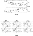
- FIG. 1 to FIG. 4 are topological structure diagrams of preferred embodiments of a first sub-module to be included in a converter provided by the present invention.
- FIG. 1 and FIG. 2 show a situation where no resistor is contained in the freewheeling diode branch.
- FIG. 3 and FIG. 4 show a situation where a resistor is contained in the freewheeling diode branch.
- the sub-module comprises turn-off devices 1, 3, 5 in antiparallel connection with diodes and an energy storage element 8, where the turn-off device 1 is in antiparallel connection with the diode 2, the turn-off device 3 is in antiparallel connection with the diode 4, and the turn-off device 5 is in antiparallel connection with the diode 6.
- Each of the turn-off devices 1, 3, 5 may be a single controlled switch device (for example, a fully controlled device such as an IGBT, an IGCT, a MOSFET or a GTO, where in the submodules provided herein, the IGBT is taken as an example) and may also be of a structure formed of at least two controlled switch devices connected in series.
- FIG. 1 shows a first sub-module 10.
- An emitter of the turn-off device 1 is connected to a collector of the turn-off device 3, with the connection point being used as a terminal X1 of the sub-module 10.
- a collector of the turn-off device 1 is connected to an emitter of the turn-off device 3 through the energy storage element 8.
- the collector of the turn-off device 1 is also connected to a cathode of a diode 7.
- An anode of the diode 7 is connected to a collector of the turn-off device 5, with the connection point being used as a terminal X2 of the sub-module 10.
- An emitter of the turn-off device 5 is connected to the emitter of the turn-off device 3.
- FIG. 2 shows another first sub-module 11.
- An emitter of a turn-off device 5 is connected to a cathode of a diode 7, with the connection point being used as a terminal X1 of the sub-module 11.
- a collector of the turn-off device 5 is connected to an anode of the diode 7 through the energy storage element 8.
- the collector of the turn-off device 5 is also connected to a collector of the turn-off device 3.
- An emitter of the turn-off device 3 is connected to a collector of the turn-off device 1, with the connection point being used as a terminal X2 of the sub-module 11.
- An emitter of the turn-off device 1 is connected to the anode of the diode 7.
- the first sub-module comprises turn-off devices 1, 3, 5 in antiparallel connection with diodes and an energy storage element C, where the turn-off device 1 is in antiparallel connection with the diode 2, the turn-off device 3 is in antiparallel connection with the diode 4, and the turn-off device 5 is in antiparallel connection with the diode 6.
- Each of the turn-off devices 1, 3, 5 may be a single controlled switch device (for example, a fully controlled device such as an IGBT, an IGCT, a MOSFET or a GTO, where in the embodiments provided herein, the IGBT is taken as an example) and may also be of a structure formed of at least two controlled switch devices connected in series.
- FIG. 3 shows a first sub-module 10'.
- a collector of the turn-off device 1 is connected to an emitter of the turn-off device 3, with the connection point being used as a terminal X1 of the sub-module 10'.
- An emitter of the turn-off device 1 is connected to a collector of the turn-off device 3 through the energy storage element C.
- the collector of the turn-off device 1 is also connected to a series resistor R and the other end of the series resistor is connected to a cathode of a diode 7.
- An anode of the diode 7 is connected to a collector of the turn-off device 5, with the connection point being used as a terminal X2 of the sub-module 10.
- the collector of the turn-off device 5 is connected to the collector of the turn-off device 3. Locations of the series resistor R and the diode 7 can be exchanged as long as it can be ensured that the anode of the diode 7 is connected to the terminal X2 directly or through the series resistor R.
- FIG. 4 shows a first sub-module 11', which is obtained by changing the topological structure of the sub-module shown in FIG. 3 in the following manner: locations of the terminal X1 and the terminal X2 in are exchanged, locations of the collector and the emitter of each turn-off device are exchanged, and locations of the anode and the cathode of each diode are exchanged.
- the collector of the turn-off device 5 is connected to the cathode of the diode 7, with the connection point being used as a terminal X1 of the sub-module 11.
- the emitter of the turn-off device 5 is connected to one end of the series resistor R through the energy storage element C and the other end of the series resistor R is connected to the anode of the diode 7.
- the collector of the turn-off device 5 is also connected to the collector of the turn-off device 3.
- the emitter of the turn-off device 3 is connected to the collector of the turn-off device 1, with the connection point being used as a terminal X2 of the sub-module 11.
- the collector of the turn-off device 1 is connected to the one end of the series resistor R. Locations of the series resistor R and the diode 7 can be exchanged as long as it can be ensured that the cathode of the diode 7 is connected to the terminal X1 directly or through the series resistor R.
- the turn-off devices, the resistor, and the freewheeling diode are described in the embodiments of the present invention. That is to say, the turn-off devices, the resistor, and the freewheeling diode can each be formed by cascading multiple elements.
- an equivalent resistor may be formed of multiple resistors connected in series or in parallel
- an equivalent freewheeling diode may be formed of multiple freewheeling diodes connected in series or in parallel, and so on.
- the series resistor is an equivalent representation, that is, the locations and the number of resistors and freewheeling diodes are not limited and the resistors and the freewheeling diodes can be arranged alternately.
- FIG. 5 shows an example of a converter useful for understanding the present invention.
- Each sub-module in the converter is one of the first submodules described above.
- the converter comprises at least one phase unit.
- the specific number of phase units can be determined according to the number of AC terminals of an AC system.
- Each of the phase units comprises an upper bridge arm 100 and a lower bridge arm 101.
- Each of the upper bridge arm and the lower bridge arm comprises at least two sub-modules 10 and at least one reactor 20 connected to each other in series.
- the number of sub-modules and reactors comprised in the upper bridge arm may be the same as or different from the number of sub-modules and reactors comprised in the lower bridge arm.
- Each sub-module 10 has two terminals X1 and X2.
- All of the sub-modules 10 in the same bridge arm are connected in the same direction and connection directions of the sub-modules in the upper bridge arm and the lower bridge arm are opposite to each other, as shown in FIG. 3 .
- One end of the upper bridge arm 100 is used as a first DC terminal P of the phase unit to be connected to a DC network.
- One end of the lower bridge arm 101 is used as a second DC terminal N of the phase unit to be connected to the DC network.
- the other ends of the upper bridge arm 100 and the lower bridge arm 101 are jointly used as an AC terminal A of the phase unit to be connected to an AC network.
- a series location of the sub-modules 10 and the reactors 20 is not limited and because one reactor can be formed of multiple reactors connected in series, the number of reactors is not limited as long as a total reactance value in a certain bridge arm meets a requirement corresponding to the bridge arm.
- sub-module 10 in Fig. 5 may also be replaced with any one of the four first sub-modules provided above.
- FIG. 6 is two topological structure diagrams of an additional (second) sub-module in the present invention.
- the cost of the converter can be reduced by replacing first sub-modules in the converter shown in FIG. 5 with the additional sub-module.
- the additional sub-module comprises turn-off devices 1, 3 in antiparallel connection with diodes and an energy storage element C, where the turn-off device 1 is in antiparallel connection with the diode 2 and the turn-off device 3 is in antiparallel connection with the diode 4.
- Each of the turn-off devices 1, 3 may be a single controlled switch device (for example, a fully controlled device such as an IGBT, an IGCT, a MOSFET or a GTO, where in the embodiments provided herein, the IGBT is taken as an example) and may also be of a structure formed of at least two controlled switch devices connected in series.
- FIG. 6(a) shows a sub-module 12. A collector of the turn-off device 1 is connected to an emitter of the turn-off device 3, with the connection point being used as a terminal X1 of the sub-module 12. An emitter of the turn-off device 1 is connected to a collector of the turn-off device 3 through the energy storage element C.
- the collector of the turn-off device 3 is used as a terminal X2 of the sub-module 12.
- FIG. 6(b) shows a sub-module 13.
- a collector of the turn-off device 3 is connected to an emitter of the turn-off device 1, with the connection point being used as a terminal X2 of the sub-module 13.
- An emitter of the turn-off device 1 is connected to a collector of the turn-off device 3 through the energy storage element C.
- the collector of the turn-off device 3 is used as a terminal X1 of the sub-module 12.
- FIG. 7 shows a preferred embodiment of a converter of the present invention, where one of the first sub-modules in the lower bridge arm of the converter shown in FIG. 5 is replaced with a second sub-module 13.
- the number of turn-off devices is reduced, thereby saving the cost of the converter.
- the converter obtained after replacement should comprise at least one first sub-module as provided by the present invention, and then any number of sub-modules of the present invention at any location in the converter shown in FIG. 5 can be replaced with an additional sub-module.
- the present invention further provides a control method for the converter as described above, where the converter is controlled by controlling an operation state of each sub-module in the converter.
- the control content of the control method is described below by taking the sub-modules 10, 11 provided in FIG. 1 and FIG. 2 of the present invention as examples.
- the control methods for the converters formed by the sub-modules 10', 11' in FIG. 3 and FIG. 4 are similar and are not described again.
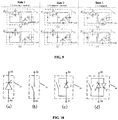
- FIG. 8(a) and FIG. 8(d) are schematic diagrams of two current directions in a state 1 respectively
- FIG. 8(b) and FIG. 8(e) are schematic diagrams of two current directions in a state 2 respectively
- FIG. 8(c) and FIG. 8(f) are schematic diagrams of two current directions in a state 3 respectively.
- the sub-module 10 is controlled to operate in the three operation states.
- the turn-off devices 1, 5 are turned on, the turn-off device 3 is turned off, and the energy storage element C is connected to the bridge arm through the diode 2 and the diode 6 (see FIG. 8(a) ) or the energy storage element C is connected to the bridge arm through the turn-off devices 5, 1 (see FIG. 8(d) ), so that an output voltage (that is, a voltage of the terminal X1 relative to terminal X2) of the sub-module 10 is a voltage across the energy storage element C.
- the turn-off devices 3, 5 are turned on and the turn-off device 1 is turned off, so that a current can flow through the turn-off device 3 and the diode 6 (see FIG. 8(b) ) or the turn-off device 5 and the diode 4 (see FIG. 8(e) ), the energy storage element C is bypassed, and an output voltage of the sub-module 10 is 0.
- the turn-off devices 1, 3, 5 are all turned off, so that when a current flows from the terminal X1 to the terminal X2, the diode 2 and the diode 6 are turned on, the energy storage element C is connected to the bridge arm through the terminal X1 and the terminal X2, and an output voltage of the sub-module 10 is a voltage across the energy storage element C (see FIG. 8(c) ); and when a current flows from the terminal X2 to the terminal X1, the diode 7 and the diode 4 are turned on, the energy storage element C is reversely connected to the bridge arm through the terminal X1 and the terminal X2 (see FIG.
- an output voltage of the sub-module 10 is a negative number of a voltage across the energy storage element C plus a voltage across the resistor.
- FIG. 9(a) and FIG. 9(d) are schematic diagrams of two current directions in a state 1 respectively
- FIG. 9(b) and FIG. 9(e) are schematic diagrams of two current directions in a state 2 respectively
- FIG. 9(c) and FIG. 9(f) are schematic diagrams of two current directions in a state 3 respectively.
- the sub-module 11 is controlled to operate in the three operation states.
- the turn-off devices 1, 5 are turned on, the turn-off device 3 is turned off, and the energy storage element C is connected to the bridge arm through the diode 6 and the diode 2 (see FIG. 9(a) ) or the energy storage element C is connected to the bridge arm through the turn-off devices 1, 5 (see FIG. 9(d) ), so that an output voltage (that is, a voltage of the terminal X1 relative to terminal X2) of the sub-module 11 is a voltage across the energy storage element C.
- the turn-off devices 3, 5 are turned on and the turn-off device 1 is turned off, so that a current can flow through the diode 6 and the turn-off device 3 (see FIG. 9(b) ) or the diode 4 and the turn-off device 5 (see FIG. 9(e) ), the energy storage element C is bypassed, and an output voltage of the sub-module 11 is 0.
- the turn-off devices 1, 3, 5 are all turned off, so that when a current flows from the terminal X1 to the terminal X2, the diode 6 and the diode 2 are turned on, the energy storage element C is connected to the bridge arm through the terminal X1 and the terminal X2, and an output voltage of the sub-module 11 is a voltage across the energy storage element C (see FIG. 9(c) ); and when a current flows from the terminal X2 to the terminal X1, the diode 4 and the diode 7 are turned on, the energy storage element C is reversely connected to the bridge arm through the terminal X1 and the terminal X2 (see FIG.
- an output voltage of the sub-module 11 is a negative number of a voltage across the energy storage element C plus a voltage across the resistor.
- the converter When a ground fault occurs in the DC network, the converter is locked so that the sub-modules 10 or 11 and possibly disposed additional sub-module 12, 13 in the converter all operate in the state 3, thereby restraining the current of a bridge arm on the failure and eventually reducing it to 0. As a result, the AC network cannot provide a fault current to a fault point.
- the fault When a transient fault occurs at the DC side, the fault can be removed without tripping an AC line switch, and a two-terminal or multi-terminal DC system formed of the converter provided by the present invention can have good ability of removing the fault at the DC side without a DC breaker.
- the converter according to the present invention further includes a protection unit.
- the protection unit is used in the first sub-module and may also be used for protecting other types of full-bridge or half-bridge sub-modules.
- the protection unit may be of four structures.
- FIG. 10(a) shows a protection unit formed of a single thyristor.
- FIG. 10(b) shows a protection unit formed of a single high-speed switch.
- FIG. 10(c) shows a protection unit formed of a thyristor and a high-speed switch connected to each other in parallel.
- FIG. 10(d) shows a protection unit formed of antiparallel thyristors and a high-speed switch connected to each other in parallel.
- FIG. 10(a) shows a protection unit 21 formed of a single thyristor, where a cathode of the thyristor is used as a terminal X3 of the protection unit 21 and an anode of the thyristor is used as a terminal X4 of the protection unit 21, so that when an overcurrent occurs in a sub-module, the protection unit 21 can be quickly turned on for shunting, thereby protecting the sub-module.
- FIG. 10(a) shows a protection unit 21 formed of a single thyristor, where a cathode of the thyristor is used as a terminal X3 of the protection unit 21 and an anode of the thyristor is used as a terminal X4 of the protection unit 21, so that when an overcurrent occurs in a sub-module, the protection unit 21 can be quickly turned on for shunting, thereby protecting the sub-module.
- FIG. 10(b) shows a protection unit 22 formed of a single high-speed switch, where one end of the high-speed switch is used as a terminal X3 of the protection unit and the other end of the high-speed switch is used as a terminal X4 of the protection unit, so that when a fault occurs in a sub-module, the faulty sub-module can be bypassed and if the bridge arm where the faulty sub-module is located has a redundant sub-module, the converter can continue to operate.
- FIG. 10(b) shows a protection unit 22 formed of a single high-speed switch, where one end of the high-speed switch is used as a terminal X3 of the protection unit and the other end of the high-speed switch is used as a terminal X4 of the protection unit, so that when a fault occurs in a sub-module, the faulty sub-module can be bypassed and if the bridge arm where the faulty sub-module is located has a redundant sub-module, the converter can continue to
- FIG. 10(c) shows a protection unit 23 formed of a thyristor and a high-speed switch connected to each other in parallel, where a cathode of the thyristor is used as a terminal X3 of the protection unit, an anode of the thyristor is used as a terminal X4 of the protection unit, one end of the high-speed switch is connected to the cathode of the thyristor, and the other end of the high-speed switch is connected to the anode of the thyristor, thereby achieving overcurrent protection and active bypassing for a sub-module.
- 10(d) shows a protection unit 24 formed of antiparallel thyristors and a high-speed switch connected to each other in parallel, where one end of the antiparallel thyristors 2' and 3' is used as a terminal X3 of the protection unit, the other end of the antiparallel thyristors 2' and 3' is used as a terminal X4 of the protection unit, one end of the high-speed switch 1' is connected to the terminal X3, and the other end of the high-speed switch 1' is connected to the terminal X4.
- the converter When a ground fault occurs in the DC network, the converter is locked so that the first sub-modules 10 or 11 in the converter all operate in the state 3, thereby restraining the current of the bridge arm on the fault and eventually reducing it to 0. As a result, the AC network cannot provide a fault current to a fault point.
- the fault When a transient fault occurs at the DC side, the fault can be removed without tripping an AC line switch, and a two-terminal or multi-terminal DC system formed of the converter provided by the present invention can have good ability of removing the fault at the DC side without a DC breaker.
Landscapes
- Engineering & Computer Science (AREA)
- Power Engineering (AREA)
- Rectifiers (AREA)
- Inverter Devices (AREA)
Applications Claiming Priority (3)
| Application Number | Priority Date | Filing Date | Title |
|---|---|---|---|
| CN201310179826.4A CN103280989B (zh) | 2013-05-15 | 2013-05-15 | 一种换流器及其控制方法 |
| PCT/CN2013/090486 WO2014183453A1 (zh) | 2013-05-15 | 2013-12-26 | 一种换流器及其控制方法 |
| PCT/CN2014/076781 WO2014183570A1 (zh) | 2013-05-15 | 2014-05-05 | 一种子模块、保护单元、换流器及其控制方法 |
Publications (3)
| Publication Number | Publication Date |
|---|---|
| EP2999103A1 EP2999103A1 (en) | 2016-03-23 |
| EP2999103A4 EP2999103A4 (en) | 2017-03-22 |
| EP2999103B1 true EP2999103B1 (en) | 2019-08-28 |
Family
ID=49063462
Family Applications (1)
| Application Number | Title | Priority Date | Filing Date |
|---|---|---|---|
| EP14797222.8A Active EP2999103B1 (en) | 2013-05-15 | 2014-05-05 | Converter and control method thereof |
Country Status (10)
| Country | Link |
|---|---|
| US (1) | US20160126827A1 (ru) |
| EP (1) | EP2999103B1 (ru) |
| KR (1) | KR102021647B1 (ru) |
| CN (1) | CN103280989B (ru) |
| CA (1) | CA2912639C (ru) |
| DK (1) | DK2999103T3 (ru) |
| ES (1) | ES2759518T3 (ru) |
| PT (1) | PT2999103T (ru) |
| RU (1) | RU2674989C2 (ru) |
| WO (2) | WO2014183453A1 (ru) |
Families Citing this family (32)
| Publication number | Priority date | Publication date | Assignee | Title |
|---|---|---|---|---|
| CN103280989B (zh) * | 2013-05-15 | 2017-02-08 | 南京南瑞继保电气有限公司 | 一种换流器及其控制方法 |
| JP6207631B2 (ja) * | 2013-12-24 | 2017-10-04 | 三菱電機株式会社 | 電力変換装置 |
| CN106030955B (zh) * | 2014-02-19 | 2019-12-17 | Abb瑞士股份有限公司 | 包括模块化多电平转换器的能量存储系统 |
| CN104868748B (zh) * | 2014-02-20 | 2017-12-22 | 南京南瑞继保电气有限公司 | 一种换流器模块单元、换流器、直流输电系统及控制方法 |
| EP3116118A4 (en) * | 2014-03-05 | 2018-03-28 | Mitsubishi Electric Corporation | Power conversion device |
| CN103825484B (zh) * | 2014-03-06 | 2016-04-20 | 华北电力大学 | 一种新型强迫换相桥路 |
| CN103904926A (zh) * | 2014-03-17 | 2014-07-02 | 华北电力大学 | 一种改进的模块化多电平换流器子模块拓扑 |
| CN104037733B (zh) * | 2014-06-03 | 2017-03-08 | 中国科学院电工研究所 | 一种直流故障隔离型柔性直流输电换流站子单元拓扑 |
| WO2015161610A1 (zh) * | 2014-04-25 | 2015-10-29 | 中国科学院电工研究所 | 直流故障隔离型柔性直流输电换流站子单元与桥臂拓扑结构 |
| CN104052026B (zh) * | 2014-05-29 | 2016-05-25 | 华中科技大学 | 用于模块化多电平换流器的子模块拓扑及其应用 |
| CN104393776B (zh) * | 2014-10-23 | 2017-07-18 | 南京南瑞继保电气有限公司 | 整流逆变单元、多电平换流器及其控制方法和控制装置 |
| EP3285388B1 (en) * | 2015-04-13 | 2021-09-22 | Mitsubishi Electric Corporation | Electric power conversion device |
| CN106329899B (zh) * | 2015-07-01 | 2018-10-16 | 南京南瑞继保电气有限公司 | 故障电流抑制阻尼器拓扑电路及其控制方法及换流器 |
| CN104993683B (zh) * | 2015-07-15 | 2018-06-19 | 南方电网科学研究院有限责任公司 | 模块化多电平换流器子模块电路 |
| EP3211784B1 (de) * | 2016-02-25 | 2021-03-31 | GE Energy Power Conversion Technology Ltd | Doppel-submodul für einen modularen mehrpunktstromrichter und modularer mehrpunktstromrichter mit diesem |
| CN105656336A (zh) * | 2016-03-30 | 2016-06-08 | 南京南瑞继保电气有限公司 | 一种降低直流侧谐波的换流器结构 |
| CN105896586B (zh) * | 2016-05-05 | 2018-08-17 | 南京南瑞继保电气有限公司 | 一种电压源换流站的故障定位及恢复方法和系统 |
| CN106058824A (zh) * | 2016-05-26 | 2016-10-26 | 华北电力大学 | 一种具备直流故障清除能力的mmc拓扑 |
| US10685761B2 (en) * | 2016-08-30 | 2020-06-16 | The Boeing Company | Electrically conductive materials |
| CN106356985A (zh) * | 2016-08-31 | 2017-01-25 | 江苏浩峰汽车附件有限公司 | 一种用于微电网的静态开关电路 |
| CN107370365B (zh) * | 2017-08-02 | 2019-09-13 | 哈尔滨工业大学 | 高压直流输电dc-dc变换器及采用该变换器实现电压充放电的方法 |
| CN108111007B (zh) * | 2018-01-31 | 2020-09-08 | 南京南瑞继保电气有限公司 | 一种功率模块冗余取能电路及控制方法 |
| EP3537584A1 (en) * | 2018-03-09 | 2019-09-11 | General Electric Technology GmbH | Voltage source converters |
| CN109546674A (zh) * | 2018-12-07 | 2019-03-29 | 南京南瑞继保电气有限公司 | 一种桥式直流耗能装置及控制方法 |
| CN112398308B (zh) * | 2019-08-14 | 2022-08-26 | 南京南瑞继保电气有限公司 | 一种多端口能量路由器及其控制系统和控制方法 |
| CN110535359A (zh) * | 2019-08-29 | 2019-12-03 | 华北电力大学(保定) | 一种具有自均压能力的二极管钳位混合mmc电路 |
| US10700617B1 (en) * | 2019-09-06 | 2020-06-30 | ABBSchweiz AG | Boosting modular multilevel converter |
| WO2021176615A1 (ja) * | 2020-03-04 | 2021-09-10 | 三菱電機株式会社 | 電力変換システム |
| JP7360987B2 (ja) | 2020-04-01 | 2023-10-13 | 株式会社ダイヘン | 溶接条件調整装置 |
| CN111934571A (zh) * | 2020-06-23 | 2020-11-13 | 中国电力科学研究院有限公司 | 一种模块化多电平变换器及其控制方法 |
| CN111917317B (zh) * | 2020-07-03 | 2022-04-26 | 上海交通大学 | 一种能阻断直流故障的柔直换流器、子模块及其保护方法 |
| CN112532057B (zh) * | 2020-12-08 | 2022-02-08 | 清华大学 | 三角形多电平变换器及其控制方法 |
Citations (2)
| Publication number | Priority date | Publication date | Assignee | Title |
|---|---|---|---|---|
| WO2011042050A1 (en) * | 2009-10-06 | 2011-04-14 | Abb Research Ltd | Modified voltage source converter structure |
| CN102957378A (zh) * | 2012-11-05 | 2013-03-06 | 郭高朋 | 基于模块化多电平变流器的高压大容量变频器系统 |
Family Cites Families (33)
| Publication number | Priority date | Publication date | Assignee | Title |
|---|---|---|---|---|
| US5986909A (en) * | 1998-05-21 | 1999-11-16 | Robicon Corporation | Multiphase power supply with plural series connected cells and failed cell bypass |
| DE20122923U1 (de) | 2001-01-24 | 2010-02-25 | Siemens Aktiengesellschaft | Stromrichterschaltungen mit verteilten Energiespeichern |
| DE10217889A1 (de) * | 2002-04-22 | 2003-11-13 | Siemens Ag | Stromversorgung mit einem Direktumrichter |
| CN100566106C (zh) * | 2003-10-17 | 2009-12-02 | Abb研究有限公司 | 用于切换大数目的切换电压电平的转换器电路 |
| DE102005040543A1 (de) * | 2005-08-26 | 2007-03-01 | Siemens Ag | Stromrichterschaltung mit verteilten Energiespeichern |
| CA2709758C (en) * | 2008-01-08 | 2016-05-10 | Abb Technology Ag | A method for controlling a voltage source converter and a voltage converting apparatus |
| BRPI0822496A2 (pt) * | 2008-03-20 | 2015-06-16 | Abb Res Ag | Conversor de fonte de voltagem |
| EP2178200B1 (en) * | 2008-10-14 | 2012-05-30 | ABB Research Ltd. | Voltage source converter with multi-level voltage output |
| CN102349223B (zh) * | 2009-03-11 | 2015-03-25 | Abb技术有限公司 | 模块化的电压源变换器 |
| EP2446527B1 (en) * | 2009-06-22 | 2015-07-01 | ALSTOM Technology Ltd | Converter |
| WO2011029480A1 (en) * | 2009-09-11 | 2011-03-17 | Abb Research Ltd | Fault current limitation in dc power transmission systems |
| DE102009057288B4 (de) * | 2009-12-01 | 2018-02-15 | Siemens Aktiengesellschaft | Umrichter für hohe Spannungen |
| EP2369725B1 (de) * | 2010-03-25 | 2012-09-26 | ABB Schweiz AG | Überbrückungseinheit |
| CN102013695A (zh) * | 2010-07-22 | 2011-04-13 | 荣信电力电子股份有限公司 | 基于h桥的无变压器风力发电并网拓扑结构 |
| PL2671297T3 (pl) * | 2011-02-01 | 2018-10-31 | Siemens Aktiengesellschaft | Sposób usuwania błędu na przewodzie prądu stałego wysokiego napięcia, instalacja do przenoszenia prądu elektrycznego przez przewód prądu stałego wysokiego napięcia i przetwornica |
| CN102170110B (zh) * | 2011-03-16 | 2014-01-29 | 中国电力科学研究院 | 一种模块化多电平换流器阀保护方法 |
| US20140226374A1 (en) * | 2011-07-29 | 2014-08-14 | Abb Technology Ag | Ctl cell protection |
| CN102299506B (zh) * | 2011-08-24 | 2014-10-29 | 中国电力科学研究院 | 一种模块化多电平换流器的保护系统及其保护方法 |
| DE102011082946B4 (de) * | 2011-09-19 | 2013-12-19 | Siemens Aktiengesellschaft | Schaltoptimierung für einen Multilevel-Generator |
| CN102427352B (zh) * | 2011-10-18 | 2013-09-04 | 吕遥 | 一种电力电子高压组合开关 |
| CN102377324B (zh) * | 2011-10-18 | 2013-09-04 | 吕遥 | 适合于高压应用的变流桥臂及其应用系统 |
| CN102611096A (zh) * | 2012-03-13 | 2012-07-25 | 浙江大学 | 一种具有直流故障自清除能力的双极直流输电系统 |
| CN102739080B (zh) * | 2012-06-21 | 2015-04-22 | 北京四方继保自动化股份有限公司 | 一种基于全桥模块化多电平变流器的直流融冰装置 |
| CN102801295B (zh) * | 2012-08-09 | 2015-01-28 | 株洲变流技术国家工程研究中心有限公司 | 一种模块化多电平换流器的子模块故障保护电路及方法 |
| CN102868290B (zh) * | 2012-09-05 | 2015-04-15 | 华北电力大学 | 全桥型mmc-hvdc子模块故障就地诊断与保护方法 |
| KR101389579B1 (ko) * | 2012-12-28 | 2014-04-29 | 주식회사 효성 | 전력용 컨버터 |
| CN103078539B (zh) * | 2013-01-15 | 2015-02-11 | 南京南瑞继保电气有限公司 | 一种模块化多电平换流器的充电方法 |
| CN103036459A (zh) * | 2013-01-15 | 2013-04-10 | 中国矿业大学(北京) | 大功率级联式多电平无桥变流器 |
| US9716425B2 (en) * | 2013-01-21 | 2017-07-25 | Abb Schweiz Ag | Multilevel converter with hybrid full-bridge cells |
| EP2768133B1 (en) * | 2013-02-14 | 2015-11-04 | ABB Technology Ltd | Converter cell with reduced power losses, high voltage multilevel converter and associated method |
| US20160036314A1 (en) * | 2013-03-18 | 2016-02-04 | Mitsubishi Electric Corporation | Power conversion apparatus |
| CN103280989B (zh) * | 2013-05-15 | 2017-02-08 | 南京南瑞继保电气有限公司 | 一种换流器及其控制方法 |
| EP2830201A1 (en) * | 2013-07-26 | 2015-01-28 | Alstom Technology Ltd | Voltage source converter module |
-
2013
- 2013-05-15 CN CN201310179826.4A patent/CN103280989B/zh active Active
- 2013-12-26 WO PCT/CN2013/090486 patent/WO2014183453A1/zh active Application Filing
-
2014
- 2014-05-05 CA CA2912639A patent/CA2912639C/en active Active
- 2014-05-05 EP EP14797222.8A patent/EP2999103B1/en active Active
- 2014-05-05 WO PCT/CN2014/076781 patent/WO2014183570A1/zh active Application Filing
- 2014-05-05 RU RU2015152358A patent/RU2674989C2/ru active
- 2014-05-05 ES ES14797222T patent/ES2759518T3/es active Active
- 2014-05-05 US US14/891,363 patent/US20160126827A1/en not_active Abandoned
- 2014-05-05 PT PT147972228T patent/PT2999103T/pt unknown
- 2014-05-05 DK DK14797222T patent/DK2999103T3/da active
- 2014-05-05 KR KR1020157035282A patent/KR102021647B1/ko active IP Right Grant
Patent Citations (2)
| Publication number | Priority date | Publication date | Assignee | Title |
|---|---|---|---|---|
| WO2011042050A1 (en) * | 2009-10-06 | 2011-04-14 | Abb Research Ltd | Modified voltage source converter structure |
| CN102957378A (zh) * | 2012-11-05 | 2013-03-06 | 郭高朋 | 基于模块化多电平变流器的高压大容量变频器系统 |
Also Published As
| Publication number | Publication date |
|---|---|
| WO2014183453A1 (zh) | 2014-11-20 |
| CA2912639C (en) | 2020-06-30 |
| KR20160026877A (ko) | 2016-03-09 |
| PT2999103T (pt) | 2019-11-15 |
| CN103280989A (zh) | 2013-09-04 |
| ES2759518T3 (es) | 2020-05-11 |
| CA2912639A1 (en) | 2014-11-20 |
| RU2015152358A3 (ru) | 2018-05-23 |
| DK2999103T3 (da) | 2019-11-04 |
| EP2999103A4 (en) | 2017-03-22 |
| RU2674989C2 (ru) | 2018-12-14 |
| EP2999103A1 (en) | 2016-03-23 |
| US20160126827A1 (en) | 2016-05-05 |
| RU2015152358A (ru) | 2017-06-20 |
| WO2014183570A1 (zh) | 2014-11-20 |
| KR102021647B1 (ko) | 2019-09-16 |
| CN103280989B (zh) | 2017-02-08 |
Similar Documents
| Publication | Publication Date | Title |
|---|---|---|
| EP2999103B1 (en) | Converter and control method thereof | |
| Wang et al. | Future HVDC-grids employing modular multilevel converters and hybrid DC-breakers | |
| KR102127036B1 (ko) | 직류 송전 보호 장치, 컨버터 및 보호 방법 | |
| KR101924707B1 (ko) | 전압원 멀티 레벨 컨버터, 직류 전력 전송 시스템 및 고장 처리 방법 및 디바이스 | |
| Wang et al. | Reactor sizing criterion for the continuous operation of meshed HB-MMC-based MTDC system under DC faults | |
| US20160268915A1 (en) | Submodule for modular multi-level converter and application thereof | |
| US8971070B2 (en) | Interface arrangement between AC and DC systems for reliable opening of the circuit breaker in time | |
| US20160226480A1 (en) | Modular Multipoint Power Converter for High Voltages | |
| KR101689824B1 (ko) | 모듈라 멀티레벨 컨버터 및 그 서브모듈 | |
| Peng et al. | A protection scheme against DC faults VSC based DC systems with bus capacitors | |
| CA2727367A1 (en) | A plant for transmitting electric power | |
| CN103986138A (zh) | 一种模块化限流断路器功率模块 | |
| CN110999064B (zh) | 具有相模块放电器的转换器装置和用于其短路保护的方法 | |
| CN112909986B (zh) | 一种模块化多电平换流器子模块及其控制方法 | |
| Yang | Protection issue discussion of DC network development: Circuit breaker or fault-tolerant converter | |
| CN111953221A (zh) | 一种模块化多电平换流器及换流站 | |
| CN112865506A (zh) | 一种具备双向故障电流切除能力的mmc双子模块 | |
| CN113258802A (zh) | 一种具备直流故障清除和自均压能力的子模块拓扑结构 | |
| CN212726884U (zh) | 一种模块化多电平换流器及换流站 | |
| CN207098600U (zh) | 换流阀子模块单元及模块化多电平换流器 | |
| Mobarrez et al. | Impact of DC side fault protection on performance and operation of multi-terminal DC (MTDC) systems | |
| Zhang et al. | A Novel MMC H-type Sub-module with Capability of DC Fault current Clearing and Voltage Self-balancing | |
| CN108462486B (zh) | 一种高压直流断路器 | |
| CN113629988A (zh) | 一种pwm整流器及其短路保护装置 | |
| CN115459613A (zh) | 一种具备直流侧故障清除能力的桥式mmc子模块拓扑及其调制方法 |
Legal Events
| Date | Code | Title | Description |
|---|---|---|---|
| PUAI | Public reference made under article 153(3) epc to a published international application that has entered the european phase |
Free format text: ORIGINAL CODE: 0009012 |
|
| 17P | Request for examination filed |
Effective date: 20151209 |
|
| AK | Designated contracting states |
Kind code of ref document: A1 Designated state(s): AL AT BE BG CH CY CZ DE DK EE ES FI FR GB GR HR HU IE IS IT LI LT LU LV MC MK MT NL NO PL PT RO RS SE SI SK SM TR |
|
| AX | Request for extension of the european patent |
Extension state: BA ME |
|
| DAX | Request for extension of the european patent (deleted) | ||
| REG | Reference to a national code |
Ref country code: DE Ref legal event code: R079 Ref document number: 602014052615 Country of ref document: DE Free format text: PREVIOUS MAIN CLASS: H02M0001000000 Ipc: H02M0001320000 |
|
| A4 | Supplementary search report drawn up and despatched |
Effective date: 20170222 |
|
| RIC1 | Information provided on ipc code assigned before grant |
Ipc: H02M 7/483 20070101ALI20170214BHEP Ipc: H02M 1/32 20070101AFI20170214BHEP |
|
| GRAP | Despatch of communication of intention to grant a patent |
Free format text: ORIGINAL CODE: EPIDOSNIGR1 |
|
| STAA | Information on the status of an ep patent application or granted ep patent |
Free format text: STATUS: GRANT OF PATENT IS INTENDED |
|
| INTG | Intention to grant announced |
Effective date: 20190621 |
|
| RAP1 | Party data changed (applicant data changed or rights of an application transferred) |
Owner name: NR ENGINEERING CO., LTD. Owner name: NR ELECTRIC CO., LTD. |
|
| RIN1 | Information on inventor provided before grant (corrected) |
Inventor name: TIAN, JIE Inventor name: WANG, NANNAN Inventor name: CAO, DONGMING Inventor name: DONG, YUNLONG Inventor name: LI, HAIYING |
|
| GRAS | Grant fee paid |
Free format text: ORIGINAL CODE: EPIDOSNIGR3 |
|
| GRAA | (expected) grant |
Free format text: ORIGINAL CODE: 0009210 |
|
| STAA | Information on the status of an ep patent application or granted ep patent |
Free format text: STATUS: THE PATENT HAS BEEN GRANTED |
|
| AK | Designated contracting states |
Kind code of ref document: B1 Designated state(s): AL AT BE BG CH CY CZ DE DK EE ES FI FR GB GR HR HU IE IS IT LI LT LU LV MC MK MT NL NO PL PT RO RS SE SI SK SM TR |
|
| REG | Reference to a national code |
Ref country code: GB Ref legal event code: FG4D |
|
| REG | Reference to a national code |
Ref country code: CH Ref legal event code: EP |
|
| REG | Reference to a national code |
Ref country code: AT Ref legal event code: REF Ref document number: 1173627 Country of ref document: AT Kind code of ref document: T Effective date: 20190915 |
|
| REG | Reference to a national code |
Ref country code: IE Ref legal event code: FG4D |
|
| REG | Reference to a national code |
Ref country code: DE Ref legal event code: R096 Ref document number: 602014052615 Country of ref document: DE |
|
| REG | Reference to a national code |
Ref country code: DK Ref legal event code: T3 Effective date: 20191031 |
|
| REG | Reference to a national code |
Ref country code: PT Ref legal event code: SC4A Ref document number: 2999103 Country of ref document: PT Date of ref document: 20191115 Kind code of ref document: T Free format text: AVAILABILITY OF NATIONAL TRANSLATION Effective date: 20191106 |
|
| REG | Reference to a national code |
Ref country code: NL Ref legal event code: FP |
|
| REG | Reference to a national code |
Ref country code: NO Ref legal event code: T2 Effective date: 20190828 |
|
| REG | Reference to a national code |
Ref country code: LT Ref legal event code: MG4D |
|
| PG25 | Lapsed in a contracting state [announced via postgrant information from national office to epo] |
Ref country code: HR Free format text: LAPSE BECAUSE OF FAILURE TO SUBMIT A TRANSLATION OF THE DESCRIPTION OR TO PAY THE FEE WITHIN THE PRESCRIBED TIME-LIMIT Effective date: 20190828 Ref country code: LT Free format text: LAPSE BECAUSE OF FAILURE TO SUBMIT A TRANSLATION OF THE DESCRIPTION OR TO PAY THE FEE WITHIN THE PRESCRIBED TIME-LIMIT Effective date: 20190828 Ref country code: FI Free format text: LAPSE BECAUSE OF FAILURE TO SUBMIT A TRANSLATION OF THE DESCRIPTION OR TO PAY THE FEE WITHIN THE PRESCRIBED TIME-LIMIT Effective date: 20190828 Ref country code: BG Free format text: LAPSE BECAUSE OF FAILURE TO SUBMIT A TRANSLATION OF THE DESCRIPTION OR TO PAY THE FEE WITHIN THE PRESCRIBED TIME-LIMIT Effective date: 20191128 Ref country code: SE Free format text: LAPSE BECAUSE OF FAILURE TO SUBMIT A TRANSLATION OF THE DESCRIPTION OR TO PAY THE FEE WITHIN THE PRESCRIBED TIME-LIMIT Effective date: 20190828 |
|
| PG25 | Lapsed in a contracting state [announced via postgrant information from national office to epo] |
Ref country code: IS Free format text: LAPSE BECAUSE OF FAILURE TO SUBMIT A TRANSLATION OF THE DESCRIPTION OR TO PAY THE FEE WITHIN THE PRESCRIBED TIME-LIMIT Effective date: 20191228 Ref country code: RS Free format text: LAPSE BECAUSE OF FAILURE TO SUBMIT A TRANSLATION OF THE DESCRIPTION OR TO PAY THE FEE WITHIN THE PRESCRIBED TIME-LIMIT Effective date: 20190828 Ref country code: LV Free format text: LAPSE BECAUSE OF FAILURE TO SUBMIT A TRANSLATION OF THE DESCRIPTION OR TO PAY THE FEE WITHIN THE PRESCRIBED TIME-LIMIT Effective date: 20190828 Ref country code: AL Free format text: LAPSE BECAUSE OF FAILURE TO SUBMIT A TRANSLATION OF THE DESCRIPTION OR TO PAY THE FEE WITHIN THE PRESCRIBED TIME-LIMIT Effective date: 20190828 |
|
| REG | Reference to a national code |
Ref country code: AT Ref legal event code: MK05 Ref document number: 1173627 Country of ref document: AT Kind code of ref document: T Effective date: 20190828 |
|
| PG25 | Lapsed in a contracting state [announced via postgrant information from national office to epo] |
Ref country code: TR Free format text: LAPSE BECAUSE OF FAILURE TO SUBMIT A TRANSLATION OF THE DESCRIPTION OR TO PAY THE FEE WITHIN THE PRESCRIBED TIME-LIMIT Effective date: 20190828 |
|
| REG | Reference to a national code |
Ref country code: GR Ref legal event code: EP Ref document number: 20190403624 Country of ref document: GR Effective date: 20200318 |
|
| PG25 | Lapsed in a contracting state [announced via postgrant information from national office to epo] |
Ref country code: PL Free format text: LAPSE BECAUSE OF FAILURE TO SUBMIT A TRANSLATION OF THE DESCRIPTION OR TO PAY THE FEE WITHIN THE PRESCRIBED TIME-LIMIT Effective date: 20190828 Ref country code: AT Free format text: LAPSE BECAUSE OF FAILURE TO SUBMIT A TRANSLATION OF THE DESCRIPTION OR TO PAY THE FEE WITHIN THE PRESCRIBED TIME-LIMIT Effective date: 20190828 Ref country code: EE Free format text: LAPSE BECAUSE OF FAILURE TO SUBMIT A TRANSLATION OF THE DESCRIPTION OR TO PAY THE FEE WITHIN THE PRESCRIBED TIME-LIMIT Effective date: 20190828 Ref country code: RO Free format text: LAPSE BECAUSE OF FAILURE TO SUBMIT A TRANSLATION OF THE DESCRIPTION OR TO PAY THE FEE WITHIN THE PRESCRIBED TIME-LIMIT Effective date: 20190828 Ref country code: IT Free format text: LAPSE BECAUSE OF FAILURE TO SUBMIT A TRANSLATION OF THE DESCRIPTION OR TO PAY THE FEE WITHIN THE PRESCRIBED TIME-LIMIT Effective date: 20190828 |
|
| REG | Reference to a national code |
Ref country code: ES Ref legal event code: FG2A Ref document number: 2759518 Country of ref document: ES Kind code of ref document: T3 Effective date: 20200511 |
|
| PG25 | Lapsed in a contracting state [announced via postgrant information from national office to epo] |
Ref country code: SM Free format text: LAPSE BECAUSE OF FAILURE TO SUBMIT A TRANSLATION OF THE DESCRIPTION OR TO PAY THE FEE WITHIN THE PRESCRIBED TIME-LIMIT Effective date: 20190828 Ref country code: CZ Free format text: LAPSE BECAUSE OF FAILURE TO SUBMIT A TRANSLATION OF THE DESCRIPTION OR TO PAY THE FEE WITHIN THE PRESCRIBED TIME-LIMIT Effective date: 20190828 Ref country code: SK Free format text: LAPSE BECAUSE OF FAILURE TO SUBMIT A TRANSLATION OF THE DESCRIPTION OR TO PAY THE FEE WITHIN THE PRESCRIBED TIME-LIMIT Effective date: 20190828 Ref country code: IS Free format text: LAPSE BECAUSE OF FAILURE TO SUBMIT A TRANSLATION OF THE DESCRIPTION OR TO PAY THE FEE WITHIN THE PRESCRIBED TIME-LIMIT Effective date: 20200224 |
|
| REG | Reference to a national code |
Ref country code: DE Ref legal event code: R097 Ref document number: 602014052615 Country of ref document: DE |
|
| PLBE | No opposition filed within time limit |
Free format text: ORIGINAL CODE: 0009261 |
|
| STAA | Information on the status of an ep patent application or granted ep patent |
Free format text: STATUS: NO OPPOSITION FILED WITHIN TIME LIMIT |
|
| PG2D | Information on lapse in contracting state deleted |
Ref country code: IS |
|
| 26N | No opposition filed |
Effective date: 20200603 |
|
| PG25 | Lapsed in a contracting state [announced via postgrant information from national office to epo] |
Ref country code: SI Free format text: LAPSE BECAUSE OF FAILURE TO SUBMIT A TRANSLATION OF THE DESCRIPTION OR TO PAY THE FEE WITHIN THE PRESCRIBED TIME-LIMIT Effective date: 20190828 |
|
| PG25 | Lapsed in a contracting state [announced via postgrant information from national office to epo] |
Ref country code: LI Free format text: LAPSE BECAUSE OF NON-PAYMENT OF DUE FEES Effective date: 20200531 Ref country code: CH Free format text: LAPSE BECAUSE OF NON-PAYMENT OF DUE FEES Effective date: 20200531 Ref country code: MC Free format text: LAPSE BECAUSE OF FAILURE TO SUBMIT A TRANSLATION OF THE DESCRIPTION OR TO PAY THE FEE WITHIN THE PRESCRIBED TIME-LIMIT Effective date: 20190828 |
|
| PG25 | Lapsed in a contracting state [announced via postgrant information from national office to epo] |
Ref country code: LU Free format text: LAPSE BECAUSE OF NON-PAYMENT OF DUE FEES Effective date: 20200505 |
|
| PG25 | Lapsed in a contracting state [announced via postgrant information from national office to epo] |
Ref country code: MT Free format text: LAPSE BECAUSE OF FAILURE TO SUBMIT A TRANSLATION OF THE DESCRIPTION OR TO PAY THE FEE WITHIN THE PRESCRIBED TIME-LIMIT Effective date: 20190828 Ref country code: CY Free format text: LAPSE BECAUSE OF FAILURE TO SUBMIT A TRANSLATION OF THE DESCRIPTION OR TO PAY THE FEE WITHIN THE PRESCRIBED TIME-LIMIT Effective date: 20190828 |
|
| PG25 | Lapsed in a contracting state [announced via postgrant information from national office to epo] |
Ref country code: MK Free format text: LAPSE BECAUSE OF FAILURE TO SUBMIT A TRANSLATION OF THE DESCRIPTION OR TO PAY THE FEE WITHIN THE PRESCRIBED TIME-LIMIT Effective date: 20190828 |
|
| PGFP | Annual fee paid to national office [announced via postgrant information from national office to epo] |
Ref country code: PT Payment date: 20230417 Year of fee payment: 10 Ref country code: NO Payment date: 20230426 Year of fee payment: 10 Ref country code: IE Payment date: 20230424 Year of fee payment: 10 Ref country code: FR Payment date: 20230523 Year of fee payment: 10 Ref country code: ES Payment date: 20230607 Year of fee payment: 10 Ref country code: DK Payment date: 20230427 Year of fee payment: 10 Ref country code: DE Payment date: 20230510 Year of fee payment: 10 |
|
| PGFP | Annual fee paid to national office [announced via postgrant information from national office to epo] |
Ref country code: GR Payment date: 20230420 Year of fee payment: 10 |
|
| PGFP | Annual fee paid to national office [announced via postgrant information from national office to epo] |
Ref country code: BE Payment date: 20230515 Year of fee payment: 10 |
|
| PGFP | Annual fee paid to national office [announced via postgrant information from national office to epo] |
Ref country code: GB Payment date: 20230519 Year of fee payment: 10 |
|
| PGFP | Annual fee paid to national office [announced via postgrant information from national office to epo] |
Ref country code: NL Payment date: 20240424 Year of fee payment: 11 |