EP2994787B1 - Verfahren und vorrichtung zur montage optischer komponenten - Google Patents
Verfahren und vorrichtung zur montage optischer komponenten Download PDFInfo
- Publication number
- EP2994787B1 EP2994787B1 EP14731320.9A EP14731320A EP2994787B1 EP 2994787 B1 EP2994787 B1 EP 2994787B1 EP 14731320 A EP14731320 A EP 14731320A EP 2994787 B1 EP2994787 B1 EP 2994787B1
- Authority
- EP
- European Patent Office
- Prior art keywords
- optic mounting
- thermally activated
- optical component
- optic
- mounting
- Prior art date
- Legal status (The legal status is an assumption and is not a legal conclusion. Google has not performed a legal analysis and makes no representation as to the accuracy of the status listed.)
- Active
Links
Images




Classifications
-
- G—PHYSICS
- G02—OPTICS
- G02B—OPTICAL ELEMENTS, SYSTEMS OR APPARATUS
- G02B6/00—Light guides; Structural details of arrangements comprising light guides and other optical elements, e.g. couplings
- G02B6/24—Coupling light guides
- G02B6/42—Coupling light guides with opto-electronic elements
- G02B6/4201—Packages, e.g. shape, construction, internal or external details
- G02B6/4219—Mechanical fixtures for holding or positioning the elements relative to each other in the couplings; Alignment methods for the elements, e.g. measuring or observing methods especially used therefor
- G02B6/4236—Fixing or mounting methods of the aligned elements
- G02B6/4238—Soldering
-
- G—PHYSICS
- G02—OPTICS
- G02B—OPTICAL ELEMENTS, SYSTEMS OR APPARATUS
- G02B6/00—Light guides; Structural details of arrangements comprising light guides and other optical elements, e.g. couplings
- G02B6/24—Coupling light guides
- G02B6/42—Coupling light guides with opto-electronic elements
- G02B6/4201—Packages, e.g. shape, construction, internal or external details
- G02B6/4219—Mechanical fixtures for holding or positioning the elements relative to each other in the couplings; Alignment methods for the elements, e.g. measuring or observing methods especially used therefor
- G02B6/4236—Fixing or mounting methods of the aligned elements
-
- G—PHYSICS
- G02—OPTICS
- G02B—OPTICAL ELEMENTS, SYSTEMS OR APPARATUS
- G02B7/00—Mountings, adjusting means, or light-tight connections, for optical elements
- G02B7/003—Alignment of optical elements
-
- B—PERFORMING OPERATIONS; TRANSPORTING
- B23—MACHINE TOOLS; METAL-WORKING NOT OTHERWISE PROVIDED FOR
- B23K—SOLDERING OR UNSOLDERING; WELDING; CLADDING OR PLATING BY SOLDERING OR WELDING; CUTTING BY APPLYING HEAT LOCALLY, e.g. FLAME CUTTING; WORKING BY LASER BEAM
- B23K1/00—Soldering, e.g. brazing, or unsoldering
- B23K1/0008—Soldering, e.g. brazing, or unsoldering specially adapted for particular articles or work
-
- G—PHYSICS
- G02—OPTICS
- G02B—OPTICAL ELEMENTS, SYSTEMS OR APPARATUS
- G02B7/00—Mountings, adjusting means, or light-tight connections, for optical elements
-
- G—PHYSICS
- G02—OPTICS
- G02B—OPTICAL ELEMENTS, SYSTEMS OR APPARATUS
- G02B7/00—Mountings, adjusting means, or light-tight connections, for optical elements
- G02B7/02—Mountings, adjusting means, or light-tight connections, for optical elements for lenses
- G02B7/023—Mountings, adjusting means, or light-tight connections, for optical elements for lenses permitting adjustment
-
- G—PHYSICS
- G02—OPTICS
- G02B—OPTICAL ELEMENTS, SYSTEMS OR APPARATUS
- G02B7/00—Mountings, adjusting means, or light-tight connections, for optical elements
- G02B7/02—Mountings, adjusting means, or light-tight connections, for optical elements for lenses
- G02B7/025—Mountings, adjusting means, or light-tight connections, for optical elements for lenses using glue
-
- G—PHYSICS
- G02—OPTICS
- G02B—OPTICAL ELEMENTS, SYSTEMS OR APPARATUS
- G02B7/00—Mountings, adjusting means, or light-tight connections, for optical elements
- G02B7/18—Mountings, adjusting means, or light-tight connections, for optical elements for prisms; for mirrors
- G02B7/182—Mountings, adjusting means, or light-tight connections, for optical elements for prisms; for mirrors for mirrors
- G02B7/1822—Mountings, adjusting means, or light-tight connections, for optical elements for prisms; for mirrors for mirrors comprising means for aligning the optical axis
Definitions
- the present invention relates to the field of optics. More specifically, the present invention concerns a method and apparatus for mounting optical components, for example the optical components employed within a laser cavity.
- An alternative technique for mounting optics known to those in the art is to employ a bonding medium on a substrate with a dedicated heating element.
- the heating element is employed to heat the bonding medium, either directly or via the substrate, as and when it is required to mount, or remove, the optical component.
- European patent publication number EP 0 196 875 describes such a system that employs a chip resistor to locally heat a solder so as to provide a means for mounting an optical component upon a substrate.
- US patent number 5,930,600 describes the use of PTC-thermistors or NTC thermistors as the heating element.
- Such elements are described as being desirable over the known resistor based heaters as they provide increased control over the heating process such that the bonding medium does not need to be heated to temperatures well above their associated melting point, thus reducing the likelihood of damage to the optical component to be mounted on, or removed from, the substrate.
- PTC-thermistors or NTC thermistors are however more expensive than the more traditional resistor based heaters thus making them less desirable for use within commercial systems.
- a further problem of employing the above described techniques lies in the fact that solders are known to cause movement during cooling between planar surfaces being secured to one another. This problem is further exacerbated when PTC-thermistors or NTC thermistors are employed since these components themselves are also known to exhibit inherent movement during periods of heating and cooling. Such movement is obviously problematic for the alignment of an optical component since it can significantly reduce the available tolerance.
- an optic mounting apparatus for mounting one or more optical components the apparatus comprising a baseplate having a first surface to which the one or more optical components are mounted and an opposing second surface characterised in that, the baseplate comprises one or more recesses arranged upon the second surface, within which are housed one or more heating elements, the location of the one or more recesses defining one or more thermally activated optic mounting areas on the first surface.
- the employment of the one or more recesses acts to reduce the thermal conduction throughout the whole of the baseplate. As a result preferential heating can be provided to the one or more thermally activated optic mounting areas while maintaining a desired mechanical strength within the baseplate.
- the baseplate may further comprise one or more recesses arranged upon the first surface or second surfaces and located around the perimeter of the one or more thermally activated optic mounting areas.
- the baseplate further comprises one or more apertures located around the perimeter of the one or more thermally activated optic mounting areas.
- the baseplate further comprises one or more ledges extending from the first surface and located around the perimeter of a thermally activated optic mounting area. Incorporation of the one or more ledges helps to retain a solder during the mounting or removal of an optical component.
- the baseplate further comprises one or more countersunk apertures. These countersunk apertures provide a means for screws to secure the optic mounting apparatus within an optical system.
- the optic mounting apparatus further comprises one or more pillars the one or pillars having a first end mechanically connected to the one or more thermally activated optic mounting areas.
- the one or more pillars may be mechanically connected to the one or more thermally activated optic mounting areas by a solder.
- the one or more pillars comprise a second end suitable for mechanical connection to an optical component.
- An adhesive may provide the mechanically connection between the second end of the one or more pillars and an optical component.
- the first end of the one or more pillars preferably comprises a rounded profile. Most preferably the first end of the one or more pillars comprises a hemispherical profile. The employment of a rounded or hemispherical profile for the first end of the pillars is found to reduce the stress placed upon the mounted optics.
- the optic mounting apparatus may further comprise one or more angled mounts suitable for mechanical attachment to one or more optical components.
- the angle of this component is chosen so as to reduce any relative movement with the associated optical component.
- the one or more angled mounts comprise a threaded aperture.
- the optic mounting apparatus may further comprise an adjustable arm at a distal end of which is located an angled mount attachment.
- the angled mount attachment provides a means for the adjustable arm to be mechanically connected to one or more angled mounts.
- the adjustable arm may further comprise an attachment arm located at its proximal end.
- the attachment arm provides a means for the adjustable arm to be mechanically connected to a reference point e.g. the wall of the housing for an optical system.
- the attachment arm comprises a dowel that provides a means for orientating the adjustable arm relative to the reference point.
- a method of mounting an optical component comprising:
- the method of mounting an optical component may further comprising providing the baseplate with one or more recesses upon the first surface or second surfaces and located around the perimeter of the one or more thermally activated optic mounting areas.
- the method of mounting an optical component further comprises providing the baseplate with one or more apertures located around the perimeter of the one or more thermally activated optic mounting areas.
- the method of mounting an optical component may further comprise providing one or more ledges extending from the first surface and located around the perimeter of a thermally activated optic mounting area.
- the method of mounting an optical component may further comprise providing the baseplate with one or more countersunk apertures.
- the one or more heating elements are located in thermal contact with the one or more thermally activated optic mounting areas by locating the one or more heating elements in one or more recesses located upon the second surface.
- a register and dowel system is employed to locate the pillar and optical component assembly within the one or more thermally activated optic mounting areas.
- Employing the register and dowel system preferably comprises mechanically attaching an angled mount to the optical component.
- Employing the register and dowel system may further comprise mechanically attaching a distal end of an adjustable arm to the angled mount.
- Employing the register and dowel system may further comprise mechanically attaching a proximal end of the adjustable arm to a reference point.
- the reference point may comprise one or more apertures located within an optical system.
- a tinning layer is applied to a first end of the pillar prior to soldering the pillar and optical component assembly to the optic mounting area.
- Embodiments of the second aspect of the invention may comprise features to implement the preferred or optional features of the first aspect of the invention or vice versa.
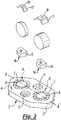
- FIG. 1 to 3 presents various representations of an optic mounting apparatus, as depicted generally by reference numeral 1.
- the mounting apparatus 1 is designed for mounting two optical components 2 e.g. a lens or a mirror. It will however be appreciated by the skilled reader that in alternative embodiments the apparatus may be adapted for the mounting a single optical component 2, or for more than two optical components 2.
- the optics mounting apparatus 1 comprises a baseplate 3 having opposing first 4 and second surfaces 5. On the first surface 4 are located two thermally activated optic mounting areas 6. The term "thermally activated" highlights the requirement within the mounting apparatus 1 for heat to be supplied in order to mount and or remove an optical component.
- the thermally activated optic mounting areas 6 may be defined by the presence of one or more apertures 7 located around its perimeter and or by a recess 8 located on the second surface 5, further details of which are described below. It is preferable for a ledge 9, that extends from the first surface 4, to also be located around the perimeter of the thermally activated optic mounting areas 6. When used in conjunction with the one or more apertures 7, the apertures 7 are positioned so as to lie outside of the area defined by the ledge 9.
- each thermally activated optic mounting area 6 comprises a circular ledge 9 and four apertures 7 wherein each aperture 7 forms an arc section that, like the circular ledge 9, is centred on the associated thermally activated optic mounting area 6. All of the apertures 7 pass all the way through the baseplate 3, although in alternative embodiments this need not necessarily be the case. From Figure 3 it can be seen each thermally activated optic mounting area 6 also comprise a recess 8 located on the second surface 5. Each recess 8 has a circular cross section that is greater in area than that of the corresponding circular ledge 9. In addition the recesses 8 are concentric with their associated circular ledge 9. The recesses 8 house a heating element 10 that is employed within the process for mounting the associated optical component 2, as described in further detail below. A standard resistor may be employed as the heating element 10 within the optic mounting apparatus 1.
- Two countersunk apertures 11 are also present on the first surface 4 of the baseplate 3.
- the countersunk apertures 11 provide a means for screws 12 to secure the optic mounting apparatus 1 within an optical system.
- the relative sizes and positions of the optic mounting areas 6 and their corresponding recesses 8 may vary.
- one or both of the raised ledges 9 may be replaced by a recessed area formed on the first surface 4.
- the optic mounting apparatus 1 further comprises a pillar 13. As best be seen from Figure 2 , a first end 14 of the pillar 13 that locates with the optic mounting areas 6 exhibits a rounded profile, and preferably a hemispherical profile.
- a layer of solder 15 is employed to secure the pillar 13 to the optic mounting area 6.
- a first layer of adhesive is employed to secure the optical component 2 to a second end 16 of the pillar 13.
- a second layer of adhesive may be employed to secure an angled mount 17 to the optical component 2. It is preferable for the mounting process, described in further detail below, for the angled mount 17 to be provided with a threaded aperture18 and to be secured to the optical component 2 such that it lies substantially opposite to the interface between the pillar 13 and the optical component 2. The angle of this component is chosen so as to reduce any relative movement with the optical component 2 to which it is attached.
- the angled mount 17 may for example exhibit a 90° angle.
- the baseplate 3 and the pillar 13 are made from a material that exhibits a low coefficient of thermal expansion.
- the preferred material for these components is Invar®.
- Invar® also known generically as FeNi 36 , is a nickel iron alloy notable in the art for its uniquely low coefficient of thermal expansion.
- the first step involves the provision of one or more of the above described thermally activated optical mounting areas 6 on the baseplate 3.
- the heating element 10 is then located in thermal contact with the thermally activated optic mounting area 6. This is preferably achieved by locating the heating element 10 within the recess 8 of the second surface 5.
- the pillar 13 and optical component 2 assembly is then located within thermally activated optic mounting area 6 and the heating element 10 is then employed to heat solder within the optic mounting area 6. This may be achieved by introducing new solder to the optic mounting area 6 at the time of applying heat, by reheating the layer of solder 15 already present within the optic mounting area 6 or via a combination of both of these procedures. When the optical component 2 is correctly aligned the heat being applied to the optic mounting area 6 is removed so that the layer of solder 15 cures, thus securing the optical component in the desired location.
- the baseplate 3 and pillar 13 are formed from Invar® it is found to be advantageous for the above described soldering process to initially tin the first end 14 of the pillar 13. Tinning assists in reducing the effects of oxidation on the first surface 14 of the pillar 13 and so allows for a more reliable and secure attachment to be made between the baseplate 3 and pillar 13.
- the pillar 13 and optical component 2 assembly could be located within the thermally activated optic mounting area 6 prior to the heating element 10 being located with the optic mounting area 6.
- the above process may further comprise the step of securing the optical component 2 to the second end 16 of the pillar 13 by introducing the first layer of adhesive.
- this process would be carried out prior to the pillar 13 and optical component 2 assembly being located within the thermally activated optical mounting area 6.
- this process could be carried out after the pillar 13 has been soldered to the baseplate 3 however such an order is less desirable since it increases the difficulty in correctly aligning the optical component 2.
- the process of locating an optical component 2 within a thermally activated optical mounting area 6 will now be described further with reference to an optical system 19, represented schematically in Figure 5 .
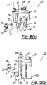
- the process employs an adjustable arm 20, various views of which can be seen in Figure 6 , that mechanically connects to an angled mount 17 so as to effectively form a register and dowel system.
- the adjustable arm 20 can be seen to comprise an attachment arm 21 and an elongated section 22 mechanically connected to each other in a substantially parallel orientation by a support bar 23 that is itself substantially perpendicular to both of the attachment arm 21 and the elongated section 22.
- the orientation of the support bar 23 defines a reference axis 24 for the adjustable arm 20.
- a dowel 27 is also mechanically attached to, and extends from, the attachment arm 21 along an axis substantially parallel to the reference axis 24. As explained below, the dowel 27 defines a reference point for the adjustable arm 20.
- a slot 28 is formed in the distal end of the elongated section 22.
- the slot 28 provides a means for setting, and securing the longitudinal position of a ball and spring mount 29 on the elongated section 22.
- a screw 30 provides the attachment means such that the ball and spring mount 29 extends from the elongated section 22 towards the attachment arm 21.
- the ball and spring mount 29 is employed to locate an angled mount attachment 31 that is shaped so as to mate with the surface of the angled mount 17 not secured to the optical component 2.
- An aperture 32 provides for a means the angled mount attachment 31 to be secured to the angled mount 17 by employing a grub screw threaded through the aperture 32 so as to locate with the threaded aperture 18 of the angled mount 17.
- the angled mount attachment 31 is located at the distal end of a sliding arm 33, the sliding arm being mechanically connected to the ball and spring mount 29 by a support 34 that is housed therein. Movement of the sliding arm 33 relative to the support 34 acts to change the spatial position of the angled mount attachment 31 along an axis substantially parallel to the reference axis 24.
- the optical system 19 can be seen to comprise a housing 35 having an external wall 36 and within which is located a baseplate 3.
- Three threaded holes 37 having a first diameter and a fourth non-threaded reference hole 38 having a second diameter are located within the external wall 36.
- the threaded holes 37 are designed to receive one or more screws 26 once these have been passed through the attachment arm 21.
- the non-threaded reference hole 38 is designed to provide an interference fit with the dowel 27 of the attachment arm 21.
- a pillar 13 and optical component 2 assembly When a pillar 13 and optical component 2 assembly is to be deployed within the system 19 it is simply attached via its angled mount 17 to the angled mount attachment 31 of the adjustable arm 20. Once attached, the dowel 27 is then located within the appropriate non-threaded reference hole 38 and one or more screws 26 are then employed the secure the adjustable arm 20 to the external wall 36 of the housing 35.
- the diameter of the non-threaded reference hole 38 is smaller than the diameter of the threaded holes 37 so as to avoid a screw 26 being inadvertently inserted into the non-threaded reference hole 38.
- the pillar 13 is located within an appropriate thermally activated optic mounting area 6 and the layer of solder 15 can then be applied as previously described.
- the layer of solder 15 has cured the angled mount attachment 31 can then be released from the angled mount 17 and adjustable arm 20 released the external wall 36 of the housing 35.
- the optical component 2 is then fixed in place with the correct optical alignment for the optical system 19.
- the design of the baseplate 3 provides the optic mounting apparatus 1 with a number of advantages over those systems known in the art.
- the employment of the apertures 7 and or the recess 8 act to reduce thermal conduction throughout the whole of the baseplate 3 and thus provide preferential heating to the optic mounting area 6 while still maintaining the desired mechanical strength. This means that lower levels of heating are required in order to melt the layer of solder 15 thus reducing the effects of thermal movement or the potential for damage to the optical component 2 itself.
- the rounded or hemispherical design of the first end 14 of the pillar 13 also provides the optic mounting apparatus 1 with a further significant advantage over the prior art systems. It is found that this shaped profile acts to significantly reduce the stress experienced by the optical component 2 once mounted on the baseplate 3.
- optical mounting apparatus 1 exhibits a significantly higher thermal stability than systems which employ optical mounting apparatus known in the art.
- laser systems employing the optical mounting apparatus 1 have been shown to exhibit significantly reduced effects of thermal drift.
- the above apparatus and methods simplify the set up of an optical system 19 and the replacement process of any optical components 2 contained therein. Indeed, the optical components 2 can be repeatedly removed from and inserted into the optical system 19 without any further adjustment being required to the alignment of the optical system 19.
- the optical components 2 can be repeatedly removed from and inserted into the optical system 19 without any further adjustment being required to the alignment of the optical system 19.
- the apparatus is suitable for mounting multiple optical components and comprises a baseplate having opposing first and second surfaces. Recesses or apertures are formed within the baseplate and are located upon the first or second surfaces so as to define thermally activated optic mounting areas. Pillars are then located within the thermally activated optic mounting areas and these provide a means for attaching the optical component to the baseplate.
- the employment of the recesses or apertures act to significantly reduce the thermal conduction throughout the baseplate. As a result preferential heating can be provided to the one or more thermally activated optic mounting areas while maintaining the baseplate with a desired mechanical strength.
- the optical mounting apparatus exhibits a high thermal stability thus making the apparatus ideally suited for use within commercial optical system.
Landscapes
- Physics & Mathematics (AREA)
- General Physics & Mathematics (AREA)
- Optics & Photonics (AREA)
- Engineering & Computer Science (AREA)
- Mechanical Engineering (AREA)
- Optical Couplings Of Light Guides (AREA)
- Mounting And Adjusting Of Optical Elements (AREA)
Claims (15)
- Eine optische Montagevorrichtung (1) zur Montage von einer oder mehreren optischen Komponenten (2) wobei die Vorrichtung eine Grundplatte (3) mit einer ersten Fläche (4), an welcher die eine oder mehreren optischen Komponenten (2) montiert sind, und einer gegenüberliegenden zweite (5) Fläche umfasst, und dadurch gekennzeichnet ist, dass,
die Grundplatte (3) eine oder mehrere Aussparungen (8) umfasst, die auf der zweiten Fläche (5) angeordnet sind und innerhalb derer sich ein oder mehrere Heizelemente (10) befinden, wobei die Lage
der einen oder mehreren Aussparungen (8) eine oder mehrere thermisch aktivierte optische Montagebereiche (6) auf der ersten Fläche (4) definiert - Eine optische Montagevorrichtung (1) nach Anspruch 1, wobei die Grundplatte (3) ferner eine oder mehrere Aussparungen oder Öffnungen (7) umfasst, die eine oder mehreren Aussparungen oder Öffnungen (7) auf der ersten Fläche (4) oder der zweiten Fläche (5) angeordnet und um den Umfang der thermisch aktivierten optischen Montagebereiche (6) positioniert sind.
- Eine optische Montagevorrichtung (1) nach einem der Ansprüche 1 oder 2, wobei die Grundplatte (3) ferner einen oder mehrere Absätze (9) umfasst, die sich von der ersten Fläche (4) erstrecken und um den Umfang eines thermisch aktivierten optischen Montagebereichs (6) positioniert sind.
- Eine optische Montagevorrichtung nach einem der vorherigen Ansprüche, wobei die Grundplatte ferner eine oder mehrere versenkte Öffnungen umfasst.
- Eine optische Montagevorrichtung (1) nach einem der vorherigen Ansprüche, wobei die optische Montagevorrichtung (1) ferner eine oder mehrere Säulen (13) umfasst, und die eine oder mehreren Säulen (13) ein erstes Ende haben, das mechanisch mit einem oder mehreren der thermisch aktivierten optischen Montagebereiche (6) verbunden ist.
- Eine optische Montagevorrichtung (1) nach Anspruch 5, wobei die eine oder mehreren Säulen (13) durch Lötzinn (15) mechanisch mit dem einen oder den mehreren thermisch aktivierten optischen Montagebereichen (6) verbunden sind.
- Eine optische Montagevorrichtung (1) nach einem der Ansprüche 5 oder 6, wobei die eine oder mehrere Säulen (13) ein zweites Ende (16) umfassen, das für die mechanische Verbindung mit einer optischen Komponente (2) geeignet ist.
- Eine optische Montagevorrichtung (1) nach einem der Ansprüche 5 bis 7, wobei das erste Ende der einen oder mehreren Säulen (13) ein abgerundetes oder halbkugelförmiges Profil (14) umfasst.
- Eine optische Montagevorrichtung (1) nach einem der vorherigen Ansprüche, wobei die optische Montagevorrichtung (1) ferner eine oder mehrere gewinkelte Halterungen (17) umfasst, die zur mechanischen Befestigung an einer oder mehreren optische Komponenten (2) geeignet sind.
- Eine optische Montagevorrichtung (1) nach einem der vorherigen Ansprüche, wobei
die optische Montagevorrichtung (1) ferner einen verstellbaren Arm (20) umfasst, an dessen distalen
Ende sich eine gewinkelte Halterungsbefestigung (31) und an dessen proximalen Ende sich ein Befestigungsarm
(21) befindet, und der Befestigungsarm (21) ein Mittel für den
verstellbaren Arm (20) zur mechanischen Verbindung mit einem Bezugspunkt (38) darstellt. - Verfahren zur Herstellung einer optischen Komponente (2), wobei das Verfahren Folgendes umfasst:- Bereitstellen einer Grundplatte (3) mit gegenüberliegenden ersten (4) und zweiten (5) Flächen mit einem oder mehreren thermisch aktivierten optischen Montagebereichen (6);- Positionieren von einem oder mehreren Heizelementen (10) in thermischem Kontakt mit dem einen oder den mehreren thermisch aktivierten optischen Montagebereichen (6);- Positionieren von einer Säule (13) und optischen Komponenten (2)-Baugruppe innerhalb des einen oder der mehreren aktivierten optischen Montagebereiche (6); und- Verwenden des einen oder der mehreren Heizelemente (10) zum Löten (15) der Säule (13) und der optischen Komponenten (2)-Baugruppe an den thermisch aktivierten optischen Montagebereich (6);- gekennzeichnet durch- Bereitstellen von einer oder mehreren Aussparungen (8) auf der zweiten Fläche (5) zur Definition des einen oder der mehreren thermisch aktivierten optischen Montagebereiche; und- Positionieren von einem oder mehreren Heizelementen (10) in der einen oder den mehreren Aussparungen (8).
- Verfahren zur Montage einer optischen Komponenten (2) nach Anspruch 11, wobei das Verfahren ferner das Bereitstellung der Grundplatte (3) mit einer oder mehreren Aussparungen oder Öffnungen (7) umfasst, und die eine oder mehrere Aussparungen oder Öffnungen (7) auf der ersten Fläche (4) oder der zweiten Fläche (5) angeordnet sind und sich auf dem Umfang der thermisch aktivierten optischen Montagebereiche (6) befinden.
- Verfahren zur Montage einer optische Komponente (2) nach einem der Ansprüche 11 oder 12, wobei das Verfahren ferner einen oder mehrere Absätze (9) umfasst, die sich von der ersten Fläche (4) erstrecken und auf dem Umfang eines thermisch aktivierten optischen Montagebereichs (6) liegen.
- Verfahren zur Montage einer optische Komponente (2) nach einem der Ansprüche 11 bis 13, wobei das Verfahren ferner ein Register- und Registerstift (27)-System umfasst, um die Säule (13) und optische Komponenten (2)-Baugruppe innerhalb des einen oder der mehreren
thermisch aktivierten optischen Montagebereichs (6) zu positionieren. - Verfahren zur Montage einer optische Komponente (2) nach einem der Ansprüche 11 bis 14, wobei das Verfahren ferner das Auftragen einer Zinnschicht auf das erste Ende der Säule (13) vor dem Löten der Säule (13) und der optischen Komponentenbaugruppe an den thermisch aktivierten optischen Montagebereich (6) umfasst.
Priority Applications (1)
| Application Number | Priority Date | Filing Date | Title |
|---|---|---|---|
| EP19210479.2A EP3640693A1 (de) | 2013-05-10 | 2014-05-09 | Verfahren und vorrichtung zum montieren von optischen bauteilen |
Applications Claiming Priority (2)
| Application Number | Priority Date | Filing Date | Title |
|---|---|---|---|
| GB1308433.0A GB2517123B (en) | 2013-05-10 | 2013-05-10 | Method and apparatus for mounting optical components |
| PCT/GB2014/051413 WO2014181116A1 (en) | 2013-05-10 | 2014-05-09 | Method and apparatus for mounting optical components |
Related Child Applications (2)
| Application Number | Title | Priority Date | Filing Date |
|---|---|---|---|
| EP19210479.2A Division EP3640693A1 (de) | 2013-05-10 | 2014-05-09 | Verfahren und vorrichtung zum montieren von optischen bauteilen |
| EP19210479.2A Division-Into EP3640693A1 (de) | 2013-05-10 | 2014-05-09 | Verfahren und vorrichtung zum montieren von optischen bauteilen |
Publications (2)
| Publication Number | Publication Date |
|---|---|
| EP2994787A1 EP2994787A1 (de) | 2016-03-16 |
| EP2994787B1 true EP2994787B1 (de) | 2020-01-01 |
Family
ID=48672120
Family Applications (2)
| Application Number | Title | Priority Date | Filing Date |
|---|---|---|---|
| EP14731320.9A Active EP2994787B1 (de) | 2013-05-10 | 2014-05-09 | Verfahren und vorrichtung zur montage optischer komponenten |
| EP19210479.2A Pending EP3640693A1 (de) | 2013-05-10 | 2014-05-09 | Verfahren und vorrichtung zum montieren von optischen bauteilen |
Family Applications After (1)
| Application Number | Title | Priority Date | Filing Date |
|---|---|---|---|
| EP19210479.2A Pending EP3640693A1 (de) | 2013-05-10 | 2014-05-09 | Verfahren und vorrichtung zum montieren von optischen bauteilen |
Country Status (7)
| Country | Link |
|---|---|
| US (2) | US11675152B2 (de) |
| EP (2) | EP2994787B1 (de) |
| JP (2) | JP6854642B2 (de) |
| CA (1) | CA2910464C (de) |
| ES (1) | ES2778043T3 (de) |
| GB (1) | GB2517123B (de) |
| WO (1) | WO2014181116A1 (de) |
Families Citing this family (5)
| Publication number | Priority date | Publication date | Assignee | Title |
|---|---|---|---|---|
| GB2517123B (en) * | 2013-05-10 | 2017-12-13 | M Squared Lasers Ltd | Method and apparatus for mounting optical components |
| US10054762B2 (en) * | 2016-12-06 | 2018-08-21 | Applied Optoelectronics, Inc. | Optical component holder having alignment feature for forming press-fit and an optical subassembly using same |
| JP7624935B2 (ja) * | 2019-05-29 | 2025-01-31 | アルコン インコーポレイティド | 光学部品取付システム |
| CN111929804B (zh) * | 2020-08-31 | 2022-03-01 | 长光卫星技术有限公司 | 一种大长宽比空间反射镜的支撑结构 |
| US20250358168A1 (en) * | 2024-05-17 | 2025-11-20 | International Business Machines Corporation | Providing on-site alerting for a data center environment |
Family Cites Families (29)
| Publication number | Priority date | Publication date | Assignee | Title |
|---|---|---|---|---|
| JPS58137293A (ja) | 1982-02-09 | 1983-08-15 | 松下電器産業株式会社 | 回路部品実装方法および回路部品実装基板 |
| GB8508280D0 (en) | 1985-03-29 | 1985-05-09 | British Telecomm | Optical component mounting |
| JPH05110242A (ja) * | 1991-10-17 | 1993-04-30 | Matsushita Electric Ind Co Ltd | 基 板 |
| JPH0650921A (ja) * | 1992-07-31 | 1994-02-25 | Nohmi Bosai Ltd | ニオイセンサ |
| JP3285294B2 (ja) * | 1995-08-08 | 2002-05-27 | 太陽誘電株式会社 | 回路モジュールの製造方法 |
| DE19613236A1 (de) | 1996-04-02 | 1997-10-09 | Coherent Adlas Gmbh & Co Kg | Modul mit befestigter Komponente und Verfahren zum Befestigen einer Komponente |
| US5891753A (en) * | 1997-01-24 | 1999-04-06 | Micron Technology, Inc. | Method and apparatus for packaging flip chip bare die on printed circuit boards |
| JPH10303516A (ja) * | 1997-04-24 | 1998-11-13 | Hitachi Ltd | プリント配線板 |
| US5896481A (en) * | 1997-05-30 | 1999-04-20 | The Boeing Company | Optical subassembly with a groove for aligning an optical device with an optical fiber |
| US5870518A (en) * | 1997-08-21 | 1999-02-09 | Mcdonnell Douglas Corporation | Microactuator for precisely aligning an optical fiber and an associated fabrication method |
| JP2000275488A (ja) * | 1999-03-25 | 2000-10-06 | Fuji Photo Film Co Ltd | 光学部材固定方法及び光学部材の支持部材 |
| EP1150152A1 (de) * | 2000-04-25 | 2001-10-31 | Hewlett-Packard Company, A Delaware Corporation | Verbindung einer optischen Baugruppe |
| US6582548B1 (en) * | 2000-07-28 | 2003-06-24 | Triquint Technology Holding Co. | Compression bonding method using laser assisted heating |
| JP2002141597A (ja) * | 2000-10-30 | 2002-05-17 | Opnext Japan Inc | 光通信モジュールおよび光通信器 |
| US6546172B2 (en) * | 2001-02-20 | 2003-04-08 | Avanti Optics Corporation | Optical device |
| US7413688B2 (en) * | 2001-09-17 | 2008-08-19 | Kenneth Noddings | Fabrication of optical devices and assemblies |
| EP1345059A1 (de) * | 2002-03-16 | 2003-09-17 | Agilent Technologies, Inc. (a Delaware corporation) | Integrierte mikrooptische Elemente |
| US6758609B2 (en) * | 2002-06-11 | 2004-07-06 | Lambda Technologies | Methods and apparatus of joining optically coupled optoelectronic and fiber optic components using electromagnetic radiation |
| US7495848B2 (en) * | 2003-07-24 | 2009-02-24 | Northrop Grumman Corporation | Cast laser optical bench |
| JP2005070553A (ja) | 2003-08-26 | 2005-03-17 | Sumitomo Electric Ind Ltd | 光デバイス、光デバイス組立装置及び光学部品の固定方法 |
| US7410088B2 (en) * | 2003-09-05 | 2008-08-12 | Matsushita Electric Industrial, Co., Ltd. | Solder preform for low heat stress laser solder attachment |
| US7021838B2 (en) | 2003-12-16 | 2006-04-04 | Matsushita Electric Industrial Co., Ltd. | Optimizing alignment of an optical fiber to an optical output port |
| DE102004038093A1 (de) | 2004-05-28 | 2005-12-22 | Osram Opto Semiconductors Gmbh | Anordnung eines mikrooptischen Bauelements auf einem Substrat, Verfahren zur Justierung der Anordnung und optisches System mit der Anordnung |
| JP4683197B2 (ja) * | 2005-03-31 | 2011-05-11 | 日本ケミコン株式会社 | チップ形コンデンサ |
| JP2006319265A (ja) | 2005-05-16 | 2006-11-24 | Sharp Corp | プリント配線基板用表面実装部品取外し装置及び該表面実装部品取外し装置を使用可能なプリント配線基板並びに該プリント配線基板の表面実装部品取外し方法 |
| JP2008021888A (ja) * | 2006-07-14 | 2008-01-31 | Nec Electronics Corp | 治具装置 |
| US8213481B2 (en) * | 2009-03-25 | 2012-07-03 | Furukawa Electric Co., Ltd. | Semiconductor laser module and manufacturing method therefor |
| US10522452B2 (en) * | 2011-10-18 | 2019-12-31 | Taiwan Semiconductor Manufacturing Company, Ltd. | Packaging methods for semiconductor devices including forming trenches in workpiece to separate adjacent packaging substrates |
| GB2517123B (en) * | 2013-05-10 | 2017-12-13 | M Squared Lasers Ltd | Method and apparatus for mounting optical components |
-
2013
- 2013-05-10 GB GB1308433.0A patent/GB2517123B/en active Active
-
2014
- 2014-05-09 US US14/889,005 patent/US11675152B2/en active Active
- 2014-05-09 ES ES14731320T patent/ES2778043T3/es active Active
- 2014-05-09 WO PCT/GB2014/051413 patent/WO2014181116A1/en not_active Ceased
- 2014-05-09 JP JP2016512417A patent/JP6854642B2/ja not_active Expired - Fee Related
- 2014-05-09 EP EP14731320.9A patent/EP2994787B1/de active Active
- 2014-05-09 CA CA2910464A patent/CA2910464C/en active Active
- 2014-05-09 EP EP19210479.2A patent/EP3640693A1/de active Pending
-
2019
- 2019-08-02 JP JP2019142774A patent/JP7330801B2/ja active Active
-
2023
- 2023-05-05 US US18/313,086 patent/US11934026B2/en active Active
Non-Patent Citations (1)
| Title |
|---|
| None * |
Also Published As
| Publication number | Publication date |
|---|---|
| GB201308433D0 (en) | 2013-06-19 |
| WO2014181116A1 (en) | 2014-11-13 |
| JP7330801B2 (ja) | 2023-08-22 |
| ES2778043T3 (es) | 2020-08-07 |
| EP2994787A1 (de) | 2016-03-16 |
| JP2016517972A (ja) | 2016-06-20 |
| EP3640693A1 (de) | 2020-04-22 |
| US20230341646A1 (en) | 2023-10-26 |
| GB2517123A (en) | 2015-02-18 |
| US20160070083A1 (en) | 2016-03-10 |
| CA2910464C (en) | 2022-06-07 |
| JP6854642B2 (ja) | 2021-04-07 |
| JP2019207425A (ja) | 2019-12-05 |
| GB2517123B (en) | 2017-12-13 |
| US11675152B2 (en) | 2023-06-13 |
| CA2910464A1 (en) | 2014-11-13 |
| US11934026B2 (en) | 2024-03-19 |
Similar Documents
| Publication | Publication Date | Title |
|---|---|---|
| US11934026B2 (en) | Method and apparatus for mounting optical components | |
| US8931684B2 (en) | Induction bonding | |
| KR102327184B1 (ko) | 열적 디포깅 시스템 및 방법 | |
| JP2016517972A5 (de) | ||
| EP0717297A2 (de) | Optisches Koppeln von Fasern an Injektionslasern | |
| EP3002619B1 (de) | Verfahren zur Montage einer Kamera | |
| JPH1056237A (ja) | 接合した部品を有するダイオードレーザモジュールおよびその接合方法 | |
| US5646674A (en) | Optical print head with flexure mounted optical device | |
| CN113260498A (zh) | 用于将功能元件安装在透镜中的方法 | |
| KR101255579B1 (ko) | 유체 배출 모듈 장착 방법 및 장치 | |
| CN111629535B (zh) | 一种用于非平面电子元件贴片的焊接装置 | |
| JP2006259727A (ja) | 低価格、高精度の複数ポイントの光学部品の取り付け法 | |
| US8785818B2 (en) | Athermalized permanent-alignment optical-element mount | |
| GB2296100A (en) | Optically coupling optical fibres to injection lasers | |
| KR101046571B1 (ko) | 고대기용 히터 | |
| CN109491033A (zh) | 用于光学器件的弹簧夹持件 | |
| US7293922B2 (en) | Non-mechanical adjustment of an optical fiber to an optical output port | |
| JP2007030044A (ja) | 保持基板上の小型部品の高精度の固定方法 | |
| JP5418362B2 (ja) | レーザ発振器、およびレーザ発振器の組立方法 | |
| WO2019118003A1 (en) | Optical mount with tilt adjustment | |
| US20040114882A1 (en) | Low cost integrated heater substrate for active optical fiber alignment | |
| JP2026071802A (ja) | レンズ加熱装置 | |
| JP2011118066A (ja) | 光ファイバ調整固定方法 | |
| JP2011060947A (ja) | 配線基板リフロー用ジグ | |
| US20130044775A1 (en) | Thermal conduction path for a heat-sensitive component |
Legal Events
| Date | Code | Title | Description |
|---|---|---|---|
| PUAI | Public reference made under article 153(3) epc to a published international application that has entered the european phase |
Free format text: ORIGINAL CODE: 0009012 |
|
| 17P | Request for examination filed |
Effective date: 20151208 |
|
| AK | Designated contracting states |
Kind code of ref document: A1 Designated state(s): AL AT BE BG CH CY CZ DE DK EE ES FI FR GB GR HR HU IE IS IT LI LT LU LV MC MK MT NL NO PL PT RO RS SE SI SK SM TR |
|
| AX | Request for extension of the european patent |
Extension state: BA ME |
|
| DAX | Request for extension of the european patent (deleted) | ||
| GRAP | Despatch of communication of intention to grant a patent |
Free format text: ORIGINAL CODE: EPIDOSNIGR1 |
|
| STAA | Information on the status of an ep patent application or granted ep patent |
Free format text: STATUS: GRANT OF PATENT IS INTENDED |
|
| RIC1 | Information provided on ipc code assigned before grant |
Ipc: G02B 7/182 20060101ALI20190627BHEP Ipc: G02B 7/02 20060101ALI20190627BHEP Ipc: B23K 1/00 20060101ALI20190627BHEP Ipc: G02B 7/00 20060101ALI20190627BHEP Ipc: G02B 6/42 20060101AFI20190627BHEP |
|
| INTG | Intention to grant announced |
Effective date: 20190718 |
|
| GRAS | Grant fee paid |
Free format text: ORIGINAL CODE: EPIDOSNIGR3 |
|
| GRAA | (expected) grant |
Free format text: ORIGINAL CODE: 0009210 |
|
| STAA | Information on the status of an ep patent application or granted ep patent |
Free format text: STATUS: THE PATENT HAS BEEN GRANTED |
|
| AK | Designated contracting states |
Kind code of ref document: B1 Designated state(s): AL AT BE BG CH CY CZ DE DK EE ES FI FR GB GR HR HU IE IS IT LI LT LU LV MC MK MT NL NO PL PT RO RS SE SI SK SM TR |
|
| REG | Reference to a national code |
Ref country code: GB Ref legal event code: FG4D |
|
| REG | Reference to a national code |
Ref country code: AT Ref legal event code: REF Ref document number: 1220492 Country of ref document: AT Kind code of ref document: T Effective date: 20200115 Ref country code: CH Ref legal event code: EP |
|
| REG | Reference to a national code |
Ref country code: IE Ref legal event code: FG4D |
|
| REG | Reference to a national code |
Ref country code: DE Ref legal event code: R096 Ref document number: 602014059278 Country of ref document: DE |
|
| REG | Reference to a national code |
Ref country code: NL Ref legal event code: FP |
|
| REG | Reference to a national code |
Ref country code: LT Ref legal event code: MG4D |
|
| PG25 | Lapsed in a contracting state [announced via postgrant information from national office to epo] |
Ref country code: FI Free format text: LAPSE BECAUSE OF FAILURE TO SUBMIT A TRANSLATION OF THE DESCRIPTION OR TO PAY THE FEE WITHIN THE PRESCRIBED TIME-LIMIT Effective date: 20200101 Ref country code: RS Free format text: LAPSE BECAUSE OF FAILURE TO SUBMIT A TRANSLATION OF THE DESCRIPTION OR TO PAY THE FEE WITHIN THE PRESCRIBED TIME-LIMIT Effective date: 20200101 Ref country code: PT Free format text: LAPSE BECAUSE OF FAILURE TO SUBMIT A TRANSLATION OF THE DESCRIPTION OR TO PAY THE FEE WITHIN THE PRESCRIBED TIME-LIMIT Effective date: 20200527 Ref country code: LT Free format text: LAPSE BECAUSE OF FAILURE TO SUBMIT A TRANSLATION OF THE DESCRIPTION OR TO PAY THE FEE WITHIN THE PRESCRIBED TIME-LIMIT Effective date: 20200101 Ref country code: CZ Free format text: LAPSE BECAUSE OF FAILURE TO SUBMIT A TRANSLATION OF THE DESCRIPTION OR TO PAY THE FEE WITHIN THE PRESCRIBED TIME-LIMIT Effective date: 20200101 Ref country code: NO Free format text: LAPSE BECAUSE OF FAILURE TO SUBMIT A TRANSLATION OF THE DESCRIPTION OR TO PAY THE FEE WITHIN THE PRESCRIBED TIME-LIMIT Effective date: 20200401 |
|
| REG | Reference to a national code |
Ref country code: ES Ref legal event code: FG2A Ref document number: 2778043 Country of ref document: ES Kind code of ref document: T3 Effective date: 20200807 |
|
| PG25 | Lapsed in a contracting state [announced via postgrant information from national office to epo] |
Ref country code: BG Free format text: LAPSE BECAUSE OF FAILURE TO SUBMIT A TRANSLATION OF THE DESCRIPTION OR TO PAY THE FEE WITHIN THE PRESCRIBED TIME-LIMIT Effective date: 20200401 Ref country code: IS Free format text: LAPSE BECAUSE OF FAILURE TO SUBMIT A TRANSLATION OF THE DESCRIPTION OR TO PAY THE FEE WITHIN THE PRESCRIBED TIME-LIMIT Effective date: 20200501 Ref country code: SE Free format text: LAPSE BECAUSE OF FAILURE TO SUBMIT A TRANSLATION OF THE DESCRIPTION OR TO PAY THE FEE WITHIN THE PRESCRIBED TIME-LIMIT Effective date: 20200101 Ref country code: LV Free format text: LAPSE BECAUSE OF FAILURE TO SUBMIT A TRANSLATION OF THE DESCRIPTION OR TO PAY THE FEE WITHIN THE PRESCRIBED TIME-LIMIT Effective date: 20200101 Ref country code: HR Free format text: LAPSE BECAUSE OF FAILURE TO SUBMIT A TRANSLATION OF THE DESCRIPTION OR TO PAY THE FEE WITHIN THE PRESCRIBED TIME-LIMIT Effective date: 20200101 Ref country code: GR Free format text: LAPSE BECAUSE OF FAILURE TO SUBMIT A TRANSLATION OF THE DESCRIPTION OR TO PAY THE FEE WITHIN THE PRESCRIBED TIME-LIMIT Effective date: 20200402 |
|
| REG | Reference to a national code |
Ref country code: DE Ref legal event code: R097 Ref document number: 602014059278 Country of ref document: DE |
|
| PG25 | Lapsed in a contracting state [announced via postgrant information from national office to epo] |
Ref country code: SK Free format text: LAPSE BECAUSE OF FAILURE TO SUBMIT A TRANSLATION OF THE DESCRIPTION OR TO PAY THE FEE WITHIN THE PRESCRIBED TIME-LIMIT Effective date: 20200101 Ref country code: DK Free format text: LAPSE BECAUSE OF FAILURE TO SUBMIT A TRANSLATION OF THE DESCRIPTION OR TO PAY THE FEE WITHIN THE PRESCRIBED TIME-LIMIT Effective date: 20200101 Ref country code: EE Free format text: LAPSE BECAUSE OF FAILURE TO SUBMIT A TRANSLATION OF THE DESCRIPTION OR TO PAY THE FEE WITHIN THE PRESCRIBED TIME-LIMIT Effective date: 20200101 Ref country code: SM Free format text: LAPSE BECAUSE OF FAILURE TO SUBMIT A TRANSLATION OF THE DESCRIPTION OR TO PAY THE FEE WITHIN THE PRESCRIBED TIME-LIMIT Effective date: 20200101 Ref country code: RO Free format text: LAPSE BECAUSE OF FAILURE TO SUBMIT A TRANSLATION OF THE DESCRIPTION OR TO PAY THE FEE WITHIN THE PRESCRIBED TIME-LIMIT Effective date: 20200101 |
|
| PLBE | No opposition filed within time limit |
Free format text: ORIGINAL CODE: 0009261 |
|
| STAA | Information on the status of an ep patent application or granted ep patent |
Free format text: STATUS: NO OPPOSITION FILED WITHIN TIME LIMIT |
|
| 26N | No opposition filed |
Effective date: 20201002 |
|
| PG25 | Lapsed in a contracting state [announced via postgrant information from national office to epo] |
Ref country code: MC Free format text: LAPSE BECAUSE OF FAILURE TO SUBMIT A TRANSLATION OF THE DESCRIPTION OR TO PAY THE FEE WITHIN THE PRESCRIBED TIME-LIMIT Effective date: 20200101 |
|
| PG25 | Lapsed in a contracting state [announced via postgrant information from national office to epo] |
Ref country code: SI Free format text: LAPSE BECAUSE OF FAILURE TO SUBMIT A TRANSLATION OF THE DESCRIPTION OR TO PAY THE FEE WITHIN THE PRESCRIBED TIME-LIMIT Effective date: 20200101 Ref country code: PL Free format text: LAPSE BECAUSE OF FAILURE TO SUBMIT A TRANSLATION OF THE DESCRIPTION OR TO PAY THE FEE WITHIN THE PRESCRIBED TIME-LIMIT Effective date: 20200101 |
|
| REG | Reference to a national code |
Ref country code: BE Ref legal event code: MM Effective date: 20200531 |
|
| PG25 | Lapsed in a contracting state [announced via postgrant information from national office to epo] |
Ref country code: LU Free format text: LAPSE BECAUSE OF NON-PAYMENT OF DUE FEES Effective date: 20200509 |
|
| PG25 | Lapsed in a contracting state [announced via postgrant information from national office to epo] |
Ref country code: BE Free format text: LAPSE BECAUSE OF NON-PAYMENT OF DUE FEES Effective date: 20200531 |
|
| PG25 | Lapsed in a contracting state [announced via postgrant information from national office to epo] |
Ref country code: TR Free format text: LAPSE BECAUSE OF FAILURE TO SUBMIT A TRANSLATION OF THE DESCRIPTION OR TO PAY THE FEE WITHIN THE PRESCRIBED TIME-LIMIT Effective date: 20200101 Ref country code: MT Free format text: LAPSE BECAUSE OF FAILURE TO SUBMIT A TRANSLATION OF THE DESCRIPTION OR TO PAY THE FEE WITHIN THE PRESCRIBED TIME-LIMIT Effective date: 20200101 Ref country code: CY Free format text: LAPSE BECAUSE OF FAILURE TO SUBMIT A TRANSLATION OF THE DESCRIPTION OR TO PAY THE FEE WITHIN THE PRESCRIBED TIME-LIMIT Effective date: 20200101 |
|
| PG25 | Lapsed in a contracting state [announced via postgrant information from national office to epo] |
Ref country code: MK Free format text: LAPSE BECAUSE OF FAILURE TO SUBMIT A TRANSLATION OF THE DESCRIPTION OR TO PAY THE FEE WITHIN THE PRESCRIBED TIME-LIMIT Effective date: 20200101 Ref country code: AL Free format text: LAPSE BECAUSE OF FAILURE TO SUBMIT A TRANSLATION OF THE DESCRIPTION OR TO PAY THE FEE WITHIN THE PRESCRIBED TIME-LIMIT Effective date: 20200101 |
|
| PGFP | Annual fee paid to national office [announced via postgrant information from national office to epo] |
Ref country code: NL Payment date: 20241111 Year of fee payment: 11 |
|
| PGFP | Annual fee paid to national office [announced via postgrant information from national office to epo] |
Ref country code: DE Payment date: 20241111 Year of fee payment: 11 |
|
| PGFP | Annual fee paid to national office [announced via postgrant information from national office to epo] |
Ref country code: GB Payment date: 20241108 Year of fee payment: 11 |
|
| PGFP | Annual fee paid to national office [announced via postgrant information from national office to epo] |
Ref country code: FR Payment date: 20241115 Year of fee payment: 11 |
|
| PGFP | Annual fee paid to national office [announced via postgrant information from national office to epo] |
Ref country code: AT Payment date: 20241125 Year of fee payment: 11 |
|
| PGFP | Annual fee paid to national office [announced via postgrant information from national office to epo] |
Ref country code: IE Payment date: 20241107 Year of fee payment: 11 |
|
| PGFP | Annual fee paid to national office [announced via postgrant information from national office to epo] |
Ref country code: IT Payment date: 20241112 Year of fee payment: 11 Ref country code: ES Payment date: 20241111 Year of fee payment: 11 |
|
| PGFP | Annual fee paid to national office [announced via postgrant information from national office to epo] |
Ref country code: CH Payment date: 20241112 Year of fee payment: 11 |
|
| REG | Reference to a national code |
Ref country code: AT Ref legal event code: UEP Ref document number: 1220492 Country of ref document: AT Kind code of ref document: T Effective date: 20200101 |
|
| REG | Reference to a national code |
Ref country code: DE Ref legal event code: R119 Ref document number: 602014059278 Country of ref document: DE |
|
| REG | Reference to a national code |
Ref country code: CH Ref legal event code: H13 Free format text: ST27 STATUS EVENT CODE: U-0-0-H10-H13 (AS PROVIDED BY THE NATIONAL OFFICE) Effective date: 20251223 |
|
| REG | Reference to a national code |
Ref country code: NL Ref legal event code: MM Effective date: 20250601 |
|
| PG25 | Lapsed in a contracting state [announced via postgrant information from national office to epo] |
Ref country code: AT Free format text: LAPSE BECAUSE OF NON-PAYMENT OF DUE FEES Effective date: 20250509 |
|
| REG | Reference to a national code |
Ref country code: AT Ref legal event code: MM01 Ref document number: 1220492 Country of ref document: AT Kind code of ref document: T Effective date: 20250509 |
|
| PG25 | Lapsed in a contracting state [announced via postgrant information from national office to epo] |
Ref country code: CH Free format text: LAPSE BECAUSE OF NON-PAYMENT OF DUE FEES Effective date: 20250531 |
|
| GBPC | Gb: european patent ceased through non-payment of renewal fee |
Effective date: 20250509 |
|
| PG25 | Lapsed in a contracting state [announced via postgrant information from national office to epo] |
Ref country code: NL Free format text: LAPSE BECAUSE OF NON-PAYMENT OF DUE FEES Effective date: 20250601 |
|
| REG | Reference to a national code |
Ref country code: GB Ref legal event code: S28 Free format text: APPLICATION FILED |
|
| PG25 | Lapsed in a contracting state [announced via postgrant information from national office to epo] |
Ref country code: GB Free format text: LAPSE BECAUSE OF NON-PAYMENT OF DUE FEES Effective date: 20250509 |
|
| PG25 | Lapsed in a contracting state [announced via postgrant information from national office to epo] |
Ref country code: DE Free format text: LAPSE BECAUSE OF NON-PAYMENT OF DUE FEES Effective date: 20251202 Ref country code: IE Free format text: LAPSE BECAUSE OF NON-PAYMENT OF DUE FEES Effective date: 20250509 |
|
| PG25 | Lapsed in a contracting state [announced via postgrant information from national office to epo] |
Ref country code: IT Free format text: LAPSE BECAUSE OF NON-PAYMENT OF DUE FEES Effective date: 20250509 |
|
| PG25 | Lapsed in a contracting state [announced via postgrant information from national office to epo] |
Ref country code: FR Free format text: LAPSE BECAUSE OF NON-PAYMENT OF DUE FEES Effective date: 20250531 |